EP4044362A1 - Connector for plastic wave guide and interconnect assembly comprising the connector - Google Patents
Connector for plastic wave guide and interconnect assembly comprising the connector Download PDFInfo
- Publication number
- EP4044362A1 EP4044362A1 EP21156713.6A EP21156713A EP4044362A1 EP 4044362 A1 EP4044362 A1 EP 4044362A1 EP 21156713 A EP21156713 A EP 21156713A EP 4044362 A1 EP4044362 A1 EP 4044362A1
- Authority
- EP
- European Patent Office
- Prior art keywords
- connector
- wave guide
- circuit board
- printed circuit
- coupler
- Prior art date
- Legal status (The legal status is an assumption and is not a legal conclusion. Google has not performed a legal analysis and makes no representation as to the accuracy of the status listed.)
- Granted
Links
Images



Classifications
-
- H—ELECTRICITY
- H01—ELECTRIC ELEMENTS
- H01P—WAVEGUIDES; RESONATORS, LINES, OR OTHER DEVICES OF THE WAVEGUIDE TYPE
- H01P5/00—Coupling devices of the waveguide type
- H01P5/08—Coupling devices of the waveguide type for linking dissimilar lines or devices
- H01P5/087—Transitions to a dielectric waveguide
-
- H—ELECTRICITY
- H01—ELECTRIC ELEMENTS
- H01P—WAVEGUIDES; RESONATORS, LINES, OR OTHER DEVICES OF THE WAVEGUIDE TYPE
- H01P5/00—Coupling devices of the waveguide type
- H01P5/08—Coupling devices of the waveguide type for linking dissimilar lines or devices
- H01P5/082—Transitions between hollow waveguides of different shape, e.g. between a rectangular and a circular waveguide
-
- H—ELECTRICITY
- H01—ELECTRIC ELEMENTS
- H01P—WAVEGUIDES; RESONATORS, LINES, OR OTHER DEVICES OF THE WAVEGUIDE TYPE
- H01P5/00—Coupling devices of the waveguide type
- H01P5/08—Coupling devices of the waveguide type for linking dissimilar lines or devices
- H01P5/10—Coupling devices of the waveguide type for linking dissimilar lines or devices for coupling balanced lines or devices with unbalanced lines or devices
- H01P5/107—Hollow-waveguide/strip-line transitions
Definitions
- the disclosure generally relates to the field of connectors, such as for example, the field of connectors for automotive vehicles.
- This disclosure also relates to an interconnect assembly comprising a printed circuit board to be connected to such a connector.
- Automotive vehicles are more and more equipped with sensors, calculators and various electronic devices.
- information signals transmitted through the information network comprising such sensors, calculators and electronic devices be reliable and not disturbed by electromagnetic interferences (EMI).
- EMI electromagnetic interferences
- Plastic waveguide communication links appear as a potential solution for automotive in the future.
- Plastic waveguides are relatively cheap compared to copper wires or optical fibres. They have many other advantages. For example, they provide a large bandwidth, they prevent EMI issues, they allow less severe alignment requirements than optical fibres (therefore they allow for a relatively easy assembly), they are compatible with CMOS circuits and they allow for coherent detection.
- the present disclosure relates to interconnect solutions for connecting plastic waveguides to printed circuit boards.
- the present disclosure provides an electrical connector according to claim 1.
- the connector of claim 1 makes it possible to mechanically secure a plastic waveguide to a printed circuit board and accommodates at least one coupler part allowing for a signal transmission between such a waveguide and a printed circuit board.
- the connector of claim 1 may combine a mechanical coupling function and a signal transmission function.
- the connector of claim 1 can be coupled and mated with a counter-connector.
- a counter-connector Several configurations can be envisioned without departing from the scope of the present disclosure.
- the coupler part and the printed circuit board can be both accommodated in the connector of claim 1, while the plastic wave guide is inserted in the tubular body of the coupler part of this connector.
- the printed circuit board is coupled to a grounded co-planar wave guide portion onto which is mounted a counter-connector.
- the plastic wave guide has a free end which is inserted in a coupler part, this coupler part having a coupling portion designed to be coupled to a substrate integrated wave guide, the coupler part (including its tubular body and its coupling portion) and the substrate integrated wave guide being both accommodated in a first connector to be mated to a second connector mounted on a printed circuit board comprising a grounded co-planar wave guide.
- the coupler part is accommodated in the connector of claim 1.
- a free end of the plastic wave guide is mechanically maintained in this connector and is inserted in the tubular body of the coupler part of this connector.
- the coupler part has also a coupling portion.
- the counter-connector can be mounted onto the printed circuit board to be coupled with the coupling portion of said connector.
- the plastic wave guide has a free end which is inserted in the tubular body of a coupler part, in a first connector.
- the coupling portion of the coupler part is coupled to a substrate integrated wave guide which is located on a printed circuit board onto which a second connector is mounted.
- This printed circuit board onto which a second connector is mounted can also comprise a grounded co-planar wave guide.
- the first and second connectors being designed to be mated.
- the coupler part is accommodated in the connector of claim 1, while a free end of the plastic wave guide is mechanically maintained in this connector and is inserted in the tubular body of the coupler part of this connector, but the coupler part also comprises a transition cavity.
- the connector of claim 1 does not necessarily comprise a printed circuit board.
- the transition cavity is extended by the coupling portion.
- a first connector accommodates the tubular body, the transition cavity and the coupling portion, the coupling portion being coupled to a grounded co-planar wave guide portion which is a portion of another circuit board onto which is mounted a second connector.
- the first and second connectors being designed to be mated.
- the coupler part is accommodated in the connector of claim 1, while the plastic wave guide is mechanically maintained in the counter-connector, with a free end extending from a coupling face of the counter-connector.
- the connector and the counter-connector are mated, the free end is inserted in the tubular body of the coupler part accommodated in the connector of claim 1.
- the connector of claim 1 can be mounted onto the printed circuit board comprising the grounded co-planar wave guide portion.
- a printed circuit board comprising a grounded co-planar wave guide portion, extended by a substrate integrated wave guide is coupled to the coupling portion of a coupler part also comprising the tubular body. At least the coupling portion and the tubular body are accommodated in a first connector.
- the substrate integrated wave guide is accommodated in the first connector too.
- the second connector only accommodates a portion of the plastic wave guide which extends through the second connector so that a free end of this plastic wave guide comes out of the face of the second connector intended to mate with the first connector.
- the coupler part which is accommodated in the connector of claim 1, can comprise all the element of a coupler, for example:
- the coupler can be integrally accommodated in the first connector only, or the coupler comprises at least one part accommodated in the second connector (for example, a substrate integrated wave guide). Or, alternatively, the coupler can be integrally accommodated in the second connector only.
- the coupler can be a rather simple structure.
- the coupler part can be made up of a metallic single piece, or it can be made up of a metallic part, designed to accommodate the end of the plastic waveguide, and a transition module made up of a printed circuit board, designed to electromagnetically couple the plastic waveguide to a microwave circuit.
- the disclosed connector may also optionally include one and / or the other of the features of any one of claims 2 to 7.
- the disclosure also relates to an interconnect assembly according to claim 8 or 9.
- an example of an interconnect assembly 1 comprises a first connector 2 and a second connector 3.
- the first connector 2 is a cable connector and the second connector 3 is an edge connector.
- the interconnect assembly 1 is designed to transmit millimetre-waves from an electronic chip 4 to a plastic wave guide 5, and vice-versa.
- the first connector 2 comprises a housing 200 having an inlet face 201 and an outlet face 202.
- the housing 200 comprises at least one alveolus 203 between the inlet face 201 and the outlet face 202, each alveolus 203 accommodating a coupler 9.
- the coupler 9 may comprise one or several parts.
- the second connector 3 is mounted on a printed circuit board 6 comprising a grounded co-planar wave guide portion 7 with a transmission line 8, and the electronic chip 4.
- the electronic chip 4 may be a CMOS chip in the form of a millimetric-wave integrated circuit.
- the first 2 and second 3 connectors are mated so that the transmission line 8 is coupled to the coupler 9.
- the coupler 9 is made of a metallic single piece designed to be accommodated in an alveolus 203 formed in the housing 200 of the first connector 2.
- the coupler 9 comprises a transition cavity 12 extending essentially between a tubular body 10 and a coupling portion 11.
- the tubular body 10 has a shape and dimensions adapted for receiving, along an insertion direction ID, the end of a plastic wave guide 5 therein.
- the tubular body 10 has, for example, a round cylindrical shape extending along an axial direction parallel to the insertion direction ID.
- the coupling portion 11 is intended to be coupled to the transmission line 8 of the printed circuit board 6.
- a wall 13 perpendicular to the insertion direction ID separates the tubular body 10 from the transition cavity 12.
- the wave signal generated by the chip 4 can be dramatically attenuated if there is a mismatch between the transmission line 8 and the plastic wave guide 5.
- an in-line configuration helps reducing the losses between the plastic wave guide 5 and the transmission line 8.
- An in-line configuration also makes easier its integration in a connector assembly.
- the transition cavity 12 of the coupler 9 has a form factor corresponding to a multi-section matching transformer, like a Chebyshev transformer or a binomial transformer. This also helps reducing the losses due to a possible mismatch between the transmission line 8 and the plastic wave guide 5.
- the coupler 9 comprises the tubular body 10, a transition wave guide portion 14 to adapt rectangular to tubular shaped portions of the coupler 9, a multi-section matching transformer section 15 and the coupling portion 11 adapted to be embedded in the printed circuit board 6.
- the tubular body 10 has an internal diameter of 3 millimetres, and is two millimetres long in a direction parallel to the insertion direction ID.
- the transition wave guide portion 14 is about 1 millimetre long in a direction parallel to the insertion direction ID and has a width of 2.6 millimetres.
- the multi-section matching transformer section 15 has four portions each about 1 millimetre long in a direction parallel to the insertion direction ID and a height decreasing respectively from 1.4 to 0.4 millimetres.
- the coupling portion 11 is about 2 millimetres long.
- the grounded co-planar wave guide 7 is 504 micrometres thick, has a 50 Ohms impedance, has a 2.2 permittivity, and a 0.0009 dielectric loss (angle ⁇ ).
- the grounded co-planar wave guide 7 is comprised, for instance, of a RT/duroid ® 5880 substrate from Rogers corporation.
- the tubular portion 10 makes it possible to avoid a plastic wave guide 5 tapered end.
- the coupling portion 11 can be inserted in the printed circuit board 6. This allows avoiding or at least limiting leakage field issues and helps strengthening the mechanical coupling between the coupler 9 and the printed circuit board 6.
- the coupler 9 comprises a horn antenna 16.
- the horn antenna 16 is conical shaped with a vertex 18 connected to the free end of the tubular body 10 (with a 3 millimetres diameter opening at the vertex), and a 10 millimetres height and 9 millimetres diameter at its base.
- the coupler 9 consists essentially of a metallic part 34.
- This metallic part 34 is made up of a metallic single piece. It comprises a tubular body 10 and a coupling portion 11, separated by a wall 13 perpendicular to the insertion direction ID.
- the tubular body 10 is similar to that of the first embodiment.
- the coupling portion 11 comprises two round cylindrical portions 19, 20. A first one 19 of these cylindrical portions 19, 20 has the same diameter as the tubular body 10 and is aligned with the tubular body 10. A second one 20 is juxtaposed to the first one 19, and has a smaller diameter. Both cylindrical portions 19, 20 are centered on the insertion direction ID.
- the coupling portion 11 also comprises a parallelepipedal intermediate portion 21 extending, in front (in the insertion direction ID) and symmetrically on opposite sides of the two round cylindrical portions 19, 20.
- the parallelepipedal intermediate portion 21 is located in front of an edge of the printed circuit board 6 onto which the second connector 3 is mounted. This edge of the printed circuit board 6 is perpendicular to the insertion direction ID (see FIGs 7 and 8 ). This edge of the printed circuit board 6 is in mechanical contact with the parallelepipedal intermediate portion 21.
- the printed circuit board 6 comprises five conductive layers 24a, 24b, 24c, 24d, 24e and four insulating layers 25a, 25b, 25c, 25d (see FIGs 5 and 6 ).
- the conductive layers 24a, 24b, 24c, 24d, 24e and the insulating layers 25a, 25b, 25c, 25d are stacked along a stacking direction SD perpendicular to the insertion direction ID.
- the stacking direction SD is perpendicular to the top 22 and bottom 23 main faces of the printed circuit board 6.
- Each one of the insulating layers 25a, 25b, 25c, 25d is respectively inserted between two adjacent conductive layers 24.
- a first insulating layer 25a is covered with a conductive layer 24a.
- the first insulating layer is for instance 0.254 millimetre thick (dimension parallel to the stacking direction SD).
- a second insulating layer 25b is stacked over the first layer 25a in the stacking direction SD, with a conductive layer 24b in between.
- the second insulating layer 25b is for instance 0.254 millimetre thick.
- a third insulating layer 25c is stacked over the second insulating layer 25b in the stacking direction SD, with a conductive layer 24c in between.
- the third insulating layer 25c is for instance 0.127 millimetre thick.
- a fourth insulating layer 25d is stacked over the third insulating layer 25c in the stacking direction SD, with a conductive layer 24d in between.
- the fourth insulating layer 25d is for instance 0.504 millimetre thick.
- the conductive layers 24a, 24b, 24c, 24d, 24e are for instance made up of copper or a copper alloy. Each conductive layer 24a, 24b, 24c, 24d, 24e is electrically connected to an adjacent one with conductive vias 26 (that is "Vertical Interconnect Access").
- the insulating layers 25a, 25b, 25c, 25d are for instance made up of glass microfiber reinforced PTFE composite. These vias 26 are designed to prevent signal leakages and limit signal losses.
- the printed circuit board 6 comprises a substrate integrated wave guide section 27 (see Figs. 6 to 8 ).
- This substrate integrated wave guide section 27 comprises a first multilayer section 28 where the five conductive layers 24a, 24b, 24c, 24d, 24e are interconnected (see FIG. 8 ).
- This first multilayer section 28 is for example 3.2 millimetres long in the insertion direction ID.
- each one of the five conductive layers 24a, 24b, 24c, 24d, 24e is interconnected to an adjacent one by virtue of two first rows of four vias 26. Each one of these two first rows is parallel to the insertion direction ID.
- Each one of these two first rows is located on an opposite side of cut-outs or etched sections 29 made in the conductive layers 24a, 24b, 24c, 24d, 24e. These etched sections 29 are staggered so as to provide an internal routing for the signal.
- the dimension of the sections 29 parallel to the insertion direction ID increases from the second conductive layer 24b to the third conductive layer 24c (which is adjacent to the second conductive layer 24b relatively to the stacking direction SD), and from the third conductive layer 24c to the fourth conductive layer 24d (which is adjacent to the third conductive layer 24c relatively to the stacking direction SD).
- the substrate integrated wave guide section 27 comprises a second multilayer section 30 where only the two upper conductive layers 24d, 24e are interconnected.
- This second multilayer section 30 is adjacent and in continuity with the first multilayer section 28 in the insertion direction ID.
- This second multilayer section 30 is for example 1.7 millimetre long in the insertion direction ID.
- two third rows of three vias 26 interconnect the two upper conductive layers 24d, 24e. These third rows spread apart from the first rows of the first multilayer section 28 up to a third multilayer section 31.
- These two third rows define a funnel shape having a narrow input end 32 and a wider flare end 33, so as to change the characteristic impedance of the cross-section, along the insertion direction ID, in order to allow for a more efficient impedance matching between the plastic wave guide 5 and the printed circuit board 6.
- the third multilayer section 31 only the two upper conductive layers 24d, 24e are interconnected.
- This third multilayer section 31 is adjacent and in continuity with the second multilayer section 30 in the insertion direction ID.
- This third multilayer section is for example 2 millimetres long in the insertion direction ID.
- two fourth rows of two vias 26 interconnect the two upper conductive layers 24d, 24e. Each one of these two fourth rows extends from a column of the second multilayer section 30 up to a grounded co-planar wave guide portion 7.
- the two fourth rows of the third multilayer section 31 narrow up to the grounded co-planar wave guide portion 7 wherein fifth rows of vias 26 are parallel and extend each respectively on one side of a transmission line 8 which joins a CMOS chip.
- the printed circuit board 6 is 504 micrometres thick, has a 50 Ohms impedance, has a 2.2 permittivity, and a 0.0009 dielectric loss (angle ⁇ ).
- the printed circuit board is comprised, for instance, of RT/duroid ® 5880 substrate from Rogers corporation.
- FIGs. 9 and 10 A third embodiment is illustrated in FIGs. 9 and 10 .
- the elements, parts, properties, functions and features of the third embodiment which are similar or identical to those already mentioned in connection with the first and second embodiments will not be repeated in detail.
- the coupler 9 is made up of two parts, a metallic part 34 comprising the tubular body 10 and a transition module 35 made up of a multilayer printed circuit board.
- the metallic part 34 and the transition module 35 are designed to be incorporated in the first connector 2.
- the metallic part 34 is similar or identical to the metallic part of the second embodiment.
- An edge of the transition module 35, perpendicular to the insertion direction ID, is located in front of the parallelepipedal intermediate portion 21. This edge of the transition module 35 is in mechanical contact with the parallelepipedal intermediate portion 21.
- the transition module 35 comprises four conductive layers 24a, 24b, 24c, 24d and three insulating layers 25a, 25b, 25c, which are structurally and dimensionally identical or similar to the respective conductive and insulating layers of the second embodiment.
- the transition module 35 comprises a first multilayer section 28 similar or identical to the first multilayer section 28 described in connection with the second embodiment.
- the first multilayer section 28 has an etched section 29 in the conductive layer 24d which is similar or identical to the one 24d described in connection with the second embodiment.
- This first multilayer section 28 is designed to be placed in front of a grounded co-planar wave guide portion 7 onto which is mounted a second connector 3 (e.g. an edge connector).
- a second connector 3 e.g. an edge connector
- the grounded co-planar wave guide portion 7 comprises a conductive layer 36 having an etched section 37.
- the dimensions of the etched section 37 are equal or greater than those of the etched section 29 of the first multilayer section 28.
- the free edge of the first multilayer section 28 is mechanically in contact with the conductive layer 36 of the grounded co-planar wave guide portion 7.
Landscapes
- Coupling Device And Connection With Printed Circuit (AREA)
- Details Of Connecting Devices For Male And Female Coupling (AREA)
Abstract
Description
- The disclosure generally relates to the field of connectors, such as for example, the field of connectors for automotive vehicles. This disclosure also relates to an interconnect assembly comprising a printed circuit board to be connected to such a connector.
- Automotive vehicles are more and more equipped with sensors, calculators and various electronic devices. Generally, it is important that the information signals transmitted through the information network comprising such sensors, calculators and electronic devices be reliable and not disturbed by electromagnetic interferences (EMI). This becomes of paramount importance when the information and the corresponding signals are used for controlling the safety, as this is the case for example for autonomous vehicles. Further, with the increasing quantity of information to be collected and managed in automotive vehicles, it is also important to keep the weight of interconnecting harnesses as low as possible.
- Plastic waveguide communication links appear as a potential solution for automotive in the future. Plastic waveguides are relatively cheap compared to copper wires or optical fibres. They have many other advantages. For example, they provide a large bandwidth, they prevent EMI issues, they allow less severe alignment requirements than optical fibres (therefore they allow for a relatively easy assembly), they are compatible with CMOS circuits and they allow for coherent detection.
- The present disclosure relates to interconnect solutions for connecting plastic waveguides to printed circuit boards.
- The present disclosure provides an electrical connector according to
claim 1. - The connector of
claim 1 makes it possible to mechanically secure a plastic waveguide to a printed circuit board and accommodates at least one coupler part allowing for a signal transmission between such a waveguide and a printed circuit board. - In other words, the connector of
claim 1 may combine a mechanical coupling function and a signal transmission function. - The connector of
claim 1 can be coupled and mated with a counter-connector. Several configurations can be envisioned without departing from the scope of the present disclosure. - For example, the coupler part and the printed circuit board can be both accommodated in the connector of
claim 1, while the plastic wave guide is inserted in the tubular body of the coupler part of this connector. In this case, the printed circuit board is coupled to a grounded co-planar wave guide portion onto which is mounted a counter-connector. In other words, the plastic wave guide has a free end which is inserted in a coupler part, this coupler part having a coupling portion designed to be coupled to a substrate integrated wave guide, the coupler part (including its tubular body and its coupling portion) and the substrate integrated wave guide being both accommodated in a first connector to be mated to a second connector mounted on a printed circuit board comprising a grounded co-planar wave guide. - Alternatively, only the coupler part is accommodated in the connector of
claim 1. A free end of the plastic wave guide is mechanically maintained in this connector and is inserted in the tubular body of the coupler part of this connector. The coupler part has also a coupling portion. The counter-connector can be mounted onto the printed circuit board to be coupled with the coupling portion of said connector. In other words, the plastic wave guide has a free end which is inserted in the tubular body of a coupler part, in a first connector. But, the coupling portion of the coupler part is coupled to a substrate integrated wave guide which is located on a printed circuit board onto which a second connector is mounted. This printed circuit board onto which a second connector is mounted can also comprise a grounded co-planar wave guide. The first and second connectors being designed to be mated. - Alternatively, the coupler part is accommodated in the connector of
claim 1, while a free end of the plastic wave guide is mechanically maintained in this connector and is inserted in the tubular body of the coupler part of this connector, but the coupler part also comprises a transition cavity. In this case, the connector ofclaim 1 does not necessarily comprise a printed circuit board. The transition cavity is extended by the coupling portion. In other words, a first connector accommodates the tubular body, the transition cavity and the coupling portion, the coupling portion being coupled to a grounded co-planar wave guide portion which is a portion of another circuit board onto which is mounted a second connector. The first and second connectors being designed to be mated. - Alternatively, the coupler part is accommodated in the connector of
claim 1, while the plastic wave guide is mechanically maintained in the counter-connector, with a free end extending from a coupling face of the counter-connector. When the connector and the counter-connector are mated, the free end is inserted in the tubular body of the coupler part accommodated in the connector ofclaim 1. In this case, the connector ofclaim 1 can be mounted onto the printed circuit board comprising the grounded co-planar wave guide portion. In other words, a printed circuit board comprising a grounded co-planar wave guide portion, extended by a substrate integrated wave guide is coupled to the coupling portion of a coupler part also comprising the tubular body. At least the coupling portion and the tubular body are accommodated in a first connector. Possibly, the substrate integrated wave guide is accommodated in the first connector too. The second connector only accommodates a portion of the plastic wave guide which extends through the second connector so that a free end of this plastic wave guide comes out of the face of the second connector intended to mate with the first connector. - The coupler part which is accommodated in the connector of
claim 1, can comprise all the element of a coupler, for example: - a tubular body, a transition cavity and a coupling portion; or
- a tubular body, a coupling portion and a substrate integrated wave guide. Alternatively, the coupler part which is accommodated in the connector of
claim 1, can comprise essentially the tubular body and the coupling portion. - In other words, the coupler can be integrally accommodated in the first connector only, or the coupler comprises at least one part accommodated in the second connector (for example, a substrate integrated wave guide). Or, alternatively, the coupler can be integrally accommodated in the second connector only. The coupler can be a rather simple structure. For example, the coupler part can be made up of a metallic single piece, or it can be made up of a metallic part, designed to accommodate the end of the plastic waveguide, and a transition module made up of a printed circuit board, designed to electromagnetically couple the plastic waveguide to a microwave circuit.
- The disclosed connector may also optionally include one and / or the other of the features of any one of
claims 2 to 7. - The disclosure also relates to an interconnect assembly according to
claim - Other features, objects and advantages of the invention will become apparent from reading the detailed description that follows, and the attached drawings, given as non-limiting examples and in which:
-
FIG. 1 is a schematic diagram illustrating the cross-section of an example of an interconnect assembly. -
FIG. 2 is a schematic perspective view of an embodiment of a coupler designed to be accommodated in a connector. -
FIG. 3 is a schematic side view of the coupler shown inFIG. 2 . -
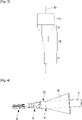
FIG. 4 is a schematic perspective view of the coupler shown inFIG. 2 andFIG. 3 , integrated between a plastic wave guide without cladding and a printed circuit board. -
FIG. 5 is a schematic perspective view of another embodiment of a coupler designed to be accommodated in a connector, in front of a schematic exploded perspective view of a multilayer printed circuit board designed to be coupled to the coupler. -
FIG. 6 is a schematic cross section of a portion of multilayer a printed circuit board designed to be coupled to the coupler shown inFIG. 5 . -
FIG. 7 is a schematic side elevation of the coupler and the multilayer printed circuit board coupled to the coupler shown inFIG. 5 . -
FIG. 8 is a schematic elevation, seen from above, of the coupler and the printed circuit board coupled to the coupler shown inFIGs. 5 and7 . -
FIG. 9 is a schematic perspective view of another embodiment of a coupler designed to be accommodated in a connector, as well as a schematic perspective view of a printed circuit board designed to be coupled to the coupler. -
FIG. 10 is another schematic perspective view of the embodiment shown onFIG. 9 , as well as a schematic perspective view of a printed circuit board designed to be coupled to the coupler. - As schematically shown in
FIG. 1 , an example of aninterconnect assembly 1 comprises afirst connector 2 and asecond connector 3. For example, thefirst connector 2 is a cable connector and thesecond connector 3 is an edge connector. For example, theinterconnect assembly 1 is designed to transmit millimetre-waves from anelectronic chip 4 to aplastic wave guide 5, and vice-versa. Thefirst connector 2 comprises ahousing 200 having aninlet face 201 and anoutlet face 202. Thehousing 200 comprises at least onealveolus 203 between theinlet face 201 and theoutlet face 202, eachalveolus 203 accommodating acoupler 9. Thecoupler 9 may comprise one or several parts. Thesecond connector 3 is mounted on a printedcircuit board 6 comprising a grounded co-planarwave guide portion 7 with atransmission line 8, and theelectronic chip 4. For example, theelectronic chip 4 may be a CMOS chip in the form of a millimetric-wave integrated circuit. The first 2 and second 3 connectors are mated so that thetransmission line 8 is coupled to thecoupler 9. - According to a first embodiment, illustrated by
FIGs. 2 to 4 , thecoupler 9 is made of a metallic single piece designed to be accommodated in analveolus 203 formed in thehousing 200 of thefirst connector 2. Thecoupler 9 comprises a transition cavity 12 extending essentially between atubular body 10 and acoupling portion 11. Thetubular body 10 has a shape and dimensions adapted for receiving, along an insertion direction ID, the end of aplastic wave guide 5 therein. Thetubular body 10 has, for example, a round cylindrical shape extending along an axial direction parallel to the insertion direction ID. Thecoupling portion 11 is intended to be coupled to thetransmission line 8 of the printedcircuit board 6. Awall 13 perpendicular to the insertion direction ID separates thetubular body 10 from the transition cavity 12. - The wave signal generated by the
chip 4 can be dramatically attenuated if there is a mismatch between thetransmission line 8 and theplastic wave guide 5. Advantageously, an in-line configuration helps reducing the losses between theplastic wave guide 5 and thetransmission line 8. An in-line configuration also makes easier its integration in a connector assembly. - Further, the transition cavity 12 of the
coupler 9 has a form factor corresponding to a multi-section matching transformer, like a Chebyshev transformer or a binomial transformer. This also helps reducing the losses due to a possible mismatch between thetransmission line 8 and theplastic wave guide 5. For example, as shown inFIGs. 2 and3 , thecoupler 9 comprises thetubular body 10, a transitionwave guide portion 14 to adapt rectangular to tubular shaped portions of thecoupler 9, a multi-sectionmatching transformer section 15 and thecoupling portion 11 adapted to be embedded in the printedcircuit board 6. For example, thetubular body 10 has an internal diameter of 3 millimetres, and is two millimetres long in a direction parallel to the insertion direction ID. For example, the transitionwave guide portion 14 is about 1 millimetre long in a direction parallel to the insertion direction ID and has a width of 2.6 millimetres. For example, the multi-section matchingtransformer section 15 has four portions each about 1 millimetre long in a direction parallel to the insertion direction ID and a height decreasing respectively from 1.4 to 0.4 millimetres. Thecoupling portion 11 is about 2 millimetres long. For example, the groundedco-planar wave guide 7 is 504 micrometres thick, has a 50 Ohms impedance, has a 2.2 permittivity, and a 0.0009 dielectric loss (angle δ). For example, the groundedco-planar wave guide 7 is comprised, for instance, of a RT/duroid® 5880 substrate from Rogers corporation. - The
tubular portion 10 makes it possible to avoid aplastic wave guide 5 tapered end. Thecoupling portion 11 can be inserted in the printedcircuit board 6. This allows avoiding or at least limiting leakage field issues and helps strengthening the mechanical coupling between thecoupler 9 and the printedcircuit board 6. - Optionally, as shown on
FIG. 4 which illustrates the case of a plastic waveguide without metallic cladding, thecoupler 9 comprises ahorn antenna 16. For example, thehorn antenna 16 is conical shaped with avertex 18 connected to the free end of the tubular body 10 (with a 3 millimetres diameter opening at the vertex), and a 10 millimetres height and 9 millimetres diameter at its base. - A second embodiment is illustrated in
FIGs. 5 to 8 . The elements, parts, properties, functions and features of the second embodiment which are similar or identical to those already mentioned in connection with the first embodiment will not be repeated in detail. Thecoupler 9 consists essentially of ametallic part 34. Thismetallic part 34 is made up of a metallic single piece. It comprises atubular body 10 and acoupling portion 11, separated by awall 13 perpendicular to the insertion direction ID. Thetubular body 10 is similar to that of the first embodiment. Thecoupling portion 11 comprises two roundcylindrical portions first one 19 of thesecylindrical portions tubular body 10 and is aligned with thetubular body 10. Asecond one 20 is juxtaposed to thefirst one 19, and has a smaller diameter. Bothcylindrical portions coupling portion 11 also comprises a parallelepipedalintermediate portion 21 extending, in front (in the insertion direction ID) and symmetrically on opposite sides of the two roundcylindrical portions - When the first 2 and second 3 connectors are mated, the parallelepipedal
intermediate portion 21 is located in front of an edge of the printedcircuit board 6 onto which thesecond connector 3 is mounted. This edge of the printedcircuit board 6 is perpendicular to the insertion direction ID (seeFIGs 7 and 8 ). This edge of the printedcircuit board 6 is in mechanical contact with the parallelepipedalintermediate portion 21. The printedcircuit board 6 comprises fiveconductive layers insulating layers FIGs 5 and 6 ). Theconductive layers layers circuit board 6. Each one of the insulatinglayers bottom face 23 of the printedcircuit board 6, a first insulatinglayer 25a is covered with aconductive layer 24a. The first insulating layer is for instance 0.254 millimetre thick (dimension parallel to the stacking direction SD). A second insulatinglayer 25b is stacked over thefirst layer 25a in the stacking direction SD, with aconductive layer 24b in between. The secondinsulating layer 25b is for instance 0.254 millimetre thick. A third insulatinglayer 25c is stacked over the second insulatinglayer 25b in the stacking direction SD, with aconductive layer 24c in between. The thirdinsulating layer 25c is for instance 0.127 millimetre thick. A fourth insulatinglayer 25d is stacked over the third insulatinglayer 25c in the stacking direction SD, with aconductive layer 24d in between. The fourth insulatinglayer 25d is for instance 0.504 millimetre thick. Theconductive layers conductive layer layers vias 26 are designed to prevent signal leakages and limit signal losses. - The printed
circuit board 6 comprises a substrate integrated wave guide section 27 (seeFigs. 6 to 8 ). This substrate integrated wave guide section 27 comprises afirst multilayer section 28 where the fiveconductive layers FIG. 8 ). Thisfirst multilayer section 28 is for example 3.2 millimetres long in the insertion direction ID. In thisfirst multilayer section 28, each one of the fiveconductive layers vias 26. Each one of these two first rows is parallel to the insertion direction ID. Each one of these two first rows is located on an opposite side of cut-outs or etchedsections 29 made in theconductive layers etched sections 29 are staggered so as to provide an internal routing for the signal. The dimension of thesections 29 parallel to the insertion direction ID increases from the secondconductive layer 24b to the thirdconductive layer 24c (which is adjacent to the secondconductive layer 24b relatively to the stacking direction SD), and from the thirdconductive layer 24c to the fourthconductive layer 24d (which is adjacent to the thirdconductive layer 24c relatively to the stacking direction SD). A second row of four vias including, at each of its ends, a via of each first row, extends perpendicular to the insertion direction ID, after eachetched sections 29. Therefore, there are three second rows of vias connecting two adjacent conductive layers through respectively the second 25b, third 25c and fourth 25d insulating layers. - The substrate integrated wave guide section 27 comprises a
second multilayer section 30 where only the two upperconductive layers second multilayer section 30 is adjacent and in continuity with thefirst multilayer section 28 in the insertion direction ID. Thissecond multilayer section 30 is for example 1.7 millimetre long in the insertion direction ID. In thissecond multilayer section 30, two third rows of threevias 26 interconnect the two upperconductive layers first multilayer section 28 up to athird multilayer section 31. These two third rows define a funnel shape having a narrow input end 32 and awider flare end 33, so as to change the characteristic impedance of the cross-section, along the insertion direction ID, in order to allow for a more efficient impedance matching between theplastic wave guide 5 and the printedcircuit board 6. - In the
third multilayer section 31, only the two upperconductive layers third multilayer section 31 is adjacent and in continuity with thesecond multilayer section 30 in the insertion direction ID. This third multilayer section is for example 2 millimetres long in the insertion direction ID. In thisthird multilayer section 31, two fourth rows of twovias 26 interconnect the two upperconductive layers second multilayer section 30 up to a grounded co-planarwave guide portion 7. The two fourth rows of thethird multilayer section 31 narrow up to the grounded co-planarwave guide portion 7 wherein fifth rows ofvias 26 are parallel and extend each respectively on one side of atransmission line 8 which joins a CMOS chip. - For example, in this second embodiment, the printed
circuit board 6 is 504 micrometres thick, has a 50 Ohms impedance, has a 2.2 permittivity, and a 0.0009 dielectric loss (angle δ). For example, the printed circuit board is comprised, for instance, of RT/duroid® 5880 substrate from Rogers corporation. - A third embodiment is illustrated in
FIGs. 9 and10 . The elements, parts, properties, functions and features of the third embodiment which are similar or identical to those already mentioned in connection with the first and second embodiments will not be repeated in detail. Thecoupler 9 is made up of two parts, ametallic part 34 comprising thetubular body 10 and atransition module 35 made up of a multilayer printed circuit board. Themetallic part 34 and thetransition module 35 are designed to be incorporated in thefirst connector 2. Themetallic part 34 is similar or identical to the metallic part of the second embodiment. An edge of thetransition module 35, perpendicular to the insertion direction ID, is located in front of the parallelepipedalintermediate portion 21. This edge of thetransition module 35 is in mechanical contact with the parallelepipedalintermediate portion 21. - For example, the
transition module 35 comprises fourconductive layers layers - The
transition module 35 comprises afirst multilayer section 28 similar or identical to thefirst multilayer section 28 described in connection with the second embodiment. In particular, thefirst multilayer section 28 has an etchedsection 29 in theconductive layer 24d which is similar or identical to the one 24d described in connection with the second embodiment. - This
first multilayer section 28 is designed to be placed in front of a grounded co-planarwave guide portion 7 onto which is mounted a second connector 3 (e.g. an edge connector). - The grounded co-planar
wave guide portion 7 comprises aconductive layer 36 having an etchedsection 37. The dimensions of the etchedsection 37 are equal or greater than those of the etchedsection 29 of thefirst multilayer section 28. - When the first 2 and second 3 connectors are mated, the free edge of the
first multilayer section 28 is mechanically in contact with theconductive layer 36 of the grounded co-planarwave guide portion 7.
Claims (9)
- Connector comprising a housing (200) with an inlet face (201) and an outlet face (202) and at least one alveolus (203) between the inlet (201) and outlet (202) faces,
characterized in that at least one coupler part (9) is accommodated in the at least one alveolus (203), the coupler part (9) being made up of an essentially metal piece extending between a tubular body (10) adapted for the insertion, along an insertion direction (ID), of an end of a plastic wave guide (5) therein, and a coupling portion (11) intended to be coupled to a printed circuit board (6). - Connector according to claim 1, wherein the at least one coupler part (9) is made up of a metallic single piece.
- Connector according to claim 1 or 2, wherein the coupling portion (11) has a parallelepipedal shape.
- Connector according to any preceding claim, wherein the at least one coupler part (9) comprises a transition cavity (12) extending between the tubular body (10) and the coupling portion (11), the transition cavity (12) having a form factor corresponding to a multi-section matching transformer.
- Connector according to claim 1, wherein the at least one coupler part (9) is made up of at least two parts comprising a metallic part (34) comprising the tubular body (10) and a transition module (35) made up of a multilayer printed circuit board.
- Connector according to claim 5, wherein the metallic part (34) comprises a parallelepipedal intermediate portion (21) extending from the tubular body (10) along the insertion direction (ID) and facing the transition module (35).
- Connector according to claim 6, wherein the transition module (35) is a multilayer printed circuit board comprising at least four conductive layers (24a, 24b, 24c, 24d, 24e) and at least three insulating layers (25a, 25b, 25c, 25d), each one of the insulating layers (25a, 25b, 25c, 25d) being respectively inserted between two adjacent conductive layers (24a, 24b, 24c, 24d, 24e), the conductive layers (24a, 24b, 24c, 24d, 24e) and the insulating layers (25a, 25b, 25c, 25d) being stacked along a stacking direction (SD) perpendicular to the insertion direction (ID), the conductive layers (24a, 24b, 24c, 24d, 24e) being electrically connected through the insulating layers (25a, 25b, 25c, 25d), wherein at least three conductive layers comprise a cutout (29) facing the parallelepipedal intermediate portion (21), the dimension of the cut-outs (29) parallel to the insertion direction (ID) increasing from a second conductive layer (24b) to a third conductive layer (24c) adjacent to the second conductive layer (24b) considered along the stacking direction (SD), and from the third conductive layer (24c) to a fourth conductive layer (24d) adjacent to the third conductive layer (24c) considered along the stacking direction (SD).
- Interconnect assembly comprising a connector according to any one of claims 1 to 6 and a printed circuit board (6) comprising a grounded co-planar wave guide portion (7).
- Interconnect assembly comprising a connector according to claim 7 and a printed circuit board (6) comprising a grounded co-planar wave guide portion (7), the transition module facing the grounded co-planar wave guide portion (7) along the insertion direction (ID).
Priority Applications (1)
| Application Number | Priority Date | Filing Date | Title |
|---|---|---|---|
| EP21156713.6A EP4044362B1 (en) | 2021-02-11 | 2021-02-11 | Connector for plastic wave guide and interconnect assembly comprising the connector |
Applications Claiming Priority (1)
| Application Number | Priority Date | Filing Date | Title |
|---|---|---|---|
| EP21156713.6A EP4044362B1 (en) | 2021-02-11 | 2021-02-11 | Connector for plastic wave guide and interconnect assembly comprising the connector |
Publications (2)
| Publication Number | Publication Date |
|---|---|
| EP4044362A1 true EP4044362A1 (en) | 2022-08-17 |
| EP4044362B1 EP4044362B1 (en) | 2026-04-01 |
Family
ID=74625801
Family Applications (1)
| Application Number | Title | Priority Date | Filing Date |
|---|---|---|---|
| EP21156713.6A Active EP4044362B1 (en) | 2021-02-11 | 2021-02-11 | Connector for plastic wave guide and interconnect assembly comprising the connector |
Country Status (1)
| Country | Link |
|---|---|
| EP (1) | EP4044362B1 (en) |
Citations (4)
| Publication number | Priority date | Publication date | Assignee | Title |
|---|---|---|---|---|
| CN201877559U (en) * | 2010-07-09 | 2011-06-22 | 广东盛路通信科技股份有限公司 | Rectangular-circular waveguide transducer for optimizing microwave antenna interface structure |
| JP2012195757A (en) * | 2011-03-16 | 2012-10-11 | Mitsubishi Electric Corp | Power supply device of post wall wave guide |
| US20150372388A1 (en) * | 2014-06-24 | 2015-12-24 | Stmicroelectronics Sa | Connector for plastic waveguide |
| US20190097294A1 (en) * | 2017-09-28 | 2019-03-28 | Te Connectivity Germany Gmbh | Plug Connection Arrangement And System Having Such Plug Connection Arrangement |
-
2021
- 2021-02-11 EP EP21156713.6A patent/EP4044362B1/en active Active
Patent Citations (4)
| Publication number | Priority date | Publication date | Assignee | Title |
|---|---|---|---|---|
| CN201877559U (en) * | 2010-07-09 | 2011-06-22 | 广东盛路通信科技股份有限公司 | Rectangular-circular waveguide transducer for optimizing microwave antenna interface structure |
| JP2012195757A (en) * | 2011-03-16 | 2012-10-11 | Mitsubishi Electric Corp | Power supply device of post wall wave guide |
| US20150372388A1 (en) * | 2014-06-24 | 2015-12-24 | Stmicroelectronics Sa | Connector for plastic waveguide |
| US20190097294A1 (en) * | 2017-09-28 | 2019-03-28 | Te Connectivity Germany Gmbh | Plug Connection Arrangement And System Having Such Plug Connection Arrangement |
Non-Patent Citations (2)
| Title |
|---|
| DE WIT MAXIME ET AL: "Polymer Microwave Fibers: A New Approach That Blends Wireline, Optical, and Wireless Communication", IEEE MICROWAVE MAGAZINE, IEEESERVICE CENTER, PISCATAWAY, NJ, US, vol. 21, no. 1, 1 January 2020 (2020-01-01), pages 51 - 66, XP011758664, ISSN: 1527-3342, [retrieved on 20191126], DOI: 10.1109/MMM.2019.2945158 * |
| LI SHENG ET AL: "A Compact Multi-layer Silicon Platelets Rectangular to Circular Waveguide Transition", 8 December 2020 (2020-12-08), pages 914 - 916, XP055821627, ISBN: 978-1-7281-6962-0, Retrieved from the Internet <URL:https://ieeexplore.ieee.org/stampPDF/getPDF.jsp?tp=&arnumber=9331624&ref=aHR0cHM6Ly9pZWVleHBsb3JlLmllZWUub3JnL3NlYXJjaC9zZWFyY2hyZXN1bHQuanNwP2FjdGlvbj1zZWFyY2gmbmV3c2VhcmNoPXRydWUmbWF0Y2hCb29sZWFuPXRydWUmcXVlcnlUZXh0PSglMjJBbGwlMjBNZXRhZGF0YSUyMjpyZWN0YW5ndWxhciUyMGNpcmN1bGFyJTIwd2F2ZWd1aWRlJTIwdHJ> [retrieved on 20210706], DOI: 10.1109/APMC47863.2020.9331624 * |
Also Published As
| Publication number | Publication date |
|---|---|
| EP4044362B1 (en) | 2026-04-01 |
Similar Documents
| Publication | Publication Date | Title |
|---|---|---|
| US9306334B2 (en) | High speed plug connector having improved high frequency performance | |
| CN108281852B (en) | Connector with Shielding Shield | |
| US8047879B2 (en) | Printed wiring boards and communication connectors having series inductor-capacitor crosstalk compensation circuits that share a common inductor | |
| CN100409503C (en) | Impedance tuned connector | |
| US7044748B2 (en) | Electrical device for interconnecting two printed circuit boards at a large distance | |
| US20160218455A1 (en) | Hybrid electrical connector for high-frequency signals | |
| EP4024624B1 (en) | Connector, connection assembly and backplane interconnection system | |
| US20170125950A1 (en) | High Speed Bypass Cable Assembly | |
| US7131862B2 (en) | Electrical connector with horizontal ground plane | |
| CN112930628B (en) | Hybrid electrical connectors for high frequency signals | |
| US10367294B1 (en) | Electrical device having a ground termination component with strain relief | |
| US9748697B2 (en) | Pluggable connector and interconnection system configured for resonance control | |
| CN102365907B (en) | Highspeed interconnection cables assembly | |
| US20020025721A1 (en) | Shielded header | |
| CN106558782B (en) | Interconnection device | |
| EP3751672A1 (en) | Compact coaxial cable connector for transmitting super high frequency signals | |
| WO2016151562A1 (en) | Hybrid electrical connector for high-frequency signals | |
| US7145083B2 (en) | Reducing or eliminating cross-talk at device-substrate interface | |
| US20110287642A1 (en) | Cable connector assembly employing separate inter connecting conductors and method for assembling the same | |
| US10003380B2 (en) | Connecting element for connecting a first data cable to a second data cable and data line having the connecting element | |
| US11876318B2 (en) | Electronic device and flat cable | |
| EP4044362B1 (en) | Connector for plastic wave guide and interconnect assembly comprising the connector | |
| JP7671357B2 (en) | Cable connectors and electronic devices | |
| EP4125152A1 (en) | Dual-mode interconnect assembly between radio-frequency integrated circuits and a plastic waveguide | |
| EP1241740A1 (en) | Conversion apparatus and method |
Legal Events
| Date | Code | Title | Description |
|---|---|---|---|
| PUAI | Public reference made under article 153(3) epc to a published international application that has entered the european phase |
Free format text: ORIGINAL CODE: 0009012 |
|
| STAA | Information on the status of an ep patent application or granted ep patent |
Free format text: STATUS: THE APPLICATION HAS BEEN PUBLISHED |
|
| AK | Designated contracting states |
Kind code of ref document: A1 Designated state(s): AL AT BE BG CH CY CZ DE DK EE ES FI FR GB GR HR HU IE IS IT LI LT LU LV MC MK MT NL NO PL PT RO RS SE SI SK SM TR |
|
| STAA | Information on the status of an ep patent application or granted ep patent |
Free format text: STATUS: REQUEST FOR EXAMINATION WAS MADE |
|
| 17P | Request for examination filed |
Effective date: 20230214 |
|
| RBV | Designated contracting states (corrected) |
Designated state(s): AL AT BE BG CH CY CZ DE DK EE ES FI FR GB GR HR HU IE IS IT LI LT LU LV MC MK MT NL NO PL PT RO RS SE SI SK SM TR |
|
| RAP3 | Party data changed (applicant data changed or rights of an application transferred) |
Owner name: CENTRALE SUPELEC Owner name: INSTITUT NATIONAL DES SCIENCES APPLIQUEES DE RENNES Owner name: UNIVERSITE DE NANTES Owner name: CENTRE NATIONAL DE LA RECHERCHE SCIENTIFIQUE Owner name: UNIVERSITE DE RENNES 1 Owner name: APTIV TECHNOLOGIES LIMITED |
|
| RAP1 | Party data changed (applicant data changed or rights of an application transferred) |
Owner name: CENTRALE SUPELEC Owner name: INSTITUT NATIONAL DES SCIENCES APPLIQUEES DE RENNES Owner name: NANTES UNIVERSITE Owner name: CENTRE NATIONAL DE LA RECHERCHE SCIENTIFIQUE Owner name: UNIVERSITE DE RENNES 1 Owner name: APTIV TECHNOLOGIES LIMITED |
|
| P01 | Opt-out of the competence of the unified patent court (upc) registered |
Effective date: 20230527 |
|
| RAP1 | Party data changed (applicant data changed or rights of an application transferred) |
Owner name: CENTRALE SUPELEC Owner name: INSTITUT NATIONAL DES SCIENCES APPLIQUEES DE RENNES Owner name: NANTES UNIVERSITE Owner name: CENTRE NATIONAL DE LA RECHERCHE SCIENTIFIQUE Owner name: UNIVERSITE DE RENNES Owner name: APTIV TECHNOLOGIES LIMITED |
|
| STAA | Information on the status of an ep patent application or granted ep patent |
Free format text: STATUS: EXAMINATION IS IN PROGRESS |
|
| 17Q | First examination report despatched |
Effective date: 20240119 |
|
| RAP1 | Party data changed (applicant data changed or rights of an application transferred) |
Owner name: CENTRALE SUPELEC Owner name: INSTITUT NATIONAL DES SCIENCES APPLIQUEES DERENNES Owner name: NANTES UNIVERSITE Owner name: CENTRE NATIONAL DE LA RECHERCHE SCIENTIFIQUE Owner name: UNIVERSITE DE RENNES Owner name: APTIV TECHNOLOGIES AG |
|
| GRAP | Despatch of communication of intention to grant a patent |
Free format text: ORIGINAL CODE: EPIDOSNIGR1 |
|
| STAA | Information on the status of an ep patent application or granted ep patent |
Free format text: STATUS: GRANT OF PATENT IS INTENDED |
|
| RIC1 | Information provided on ipc code assigned before grant |
Ipc: H01P 5/08 20060101AFI20250912BHEP Ipc: H01P 5/107 20060101ALN20250912BHEP |
|
| INTG | Intention to grant announced |
Effective date: 20251010 |
|
| GRAS | Grant fee paid |
Free format text: ORIGINAL CODE: EPIDOSNIGR3 |
|
| RAP3 | Party data changed (applicant data changed or rights of an application transferred) |
Owner name: APTIV TECHNOLOGIES AG Owner name: UNIVERSITE DE RENNES Owner name: CENTRE NATIONAL DE LA RECHERCHE SCIENTIFIQUE Owner name: NANTES UNIVERSITE Owner name: INSTITUT NATIONAL DES SCIENCES APPLIQUEES DERENNES Owner name: CENTRALE SUPELEC |
|
| GRAA | (expected) grant |
Free format text: ORIGINAL CODE: 0009210 |
|
| STAA | Information on the status of an ep patent application or granted ep patent |
Free format text: STATUS: THE PATENT HAS BEEN GRANTED |
|
| AK | Designated contracting states |
Kind code of ref document: B1 Designated state(s): AL AT BE BG CH CY CZ DE DK EE ES FI FR GB GR HR HU IE IS IT LI LT LU LV MC MK MT NL NO PL PT RO RS SE SI SK SM TR |
|
| REG | Reference to a national code |
Ref country code: CH Ref legal event code: F10 Free format text: ST27 STATUS EVENT CODE: U-0-0-F10-F00 (AS PROVIDED BY THE NATIONAL OFFICE) Effective date: 20260401 Ref country code: GB Ref legal event code: FG4D |
|
| REG | Reference to a national code |
Ref country code: DE Ref legal event code: R096 Ref document number: 602021050954 Country of ref document: DE |
|
| REG | Reference to a national code |
Ref country code: IE Ref legal event code: FG4D |