EP4044207A1 - Electronic device - Google Patents
Electronic device Download PDFInfo
- Publication number
- EP4044207A1 EP4044207A1 EP20891839.1A EP20891839A EP4044207A1 EP 4044207 A1 EP4044207 A1 EP 4044207A1 EP 20891839 A EP20891839 A EP 20891839A EP 4044207 A1 EP4044207 A1 EP 4044207A1
- Authority
- EP
- European Patent Office
- Prior art keywords
- slot
- limiting
- face
- plate
- side wall
- Prior art date
- Legal status (The legal status is an assumption and is not a legal conclusion. Google has not performed a legal analysis and makes no representation as to the accuracy of the status listed.)
- Granted
Links
Images





Classifications
-
- H—ELECTRICITY
- H05—ELECTRIC TECHNIQUES NOT OTHERWISE PROVIDED FOR
- H05K—PRINTED CIRCUITS; CASINGS OR CONSTRUCTIONAL DETAILS OF ELECTRIC APPARATUS; MANUFACTURE OF ASSEMBLAGES OF ELECTRICAL COMPONENTS
- H05K5/00—Casings, cabinets or drawers for electric apparatus
- H05K5/02—Details
- H05K5/0247—Electrical details of casings, e.g. terminals, passages for cables or wiring
-
- G—PHYSICS
- G06—COMPUTING OR CALCULATING; COUNTING
- G06F—ELECTRIC DIGITAL DATA PROCESSING
- G06F1/00—Details not covered by groups G06F3/00 - G06F13/00 and G06F21/00
- G06F1/16—Constructional details or arrangements
- G06F1/1613—Constructional details or arrangements for portable computers
- G06F1/1633—Constructional details or arrangements of portable computers not specific to the type of enclosures covered by groups G06F1/1615 - G06F1/1626
- G06F1/1656—Details related to functional adaptations of the enclosure, e.g. to provide protection against EMI, shock, water, or to host detachable peripherals like a mouse or removable expansions units like PCMCIA cards, or to provide access to internal components for maintenance or to removable storage supports like CDs or DVDs, or to mechanically mount accessories
- G06F1/1658—Details related to functional adaptations of the enclosure, e.g. to provide protection against EMI, shock, water, or to host detachable peripherals like a mouse or removable expansions units like PCMCIA cards, or to provide access to internal components for maintenance or to removable storage supports like CDs or DVDs, or to mechanically mount accessories related to the mounting of internal components, e.g. disc drive or any other functional module
-
- G—PHYSICS
- G06—COMPUTING OR CALCULATING; COUNTING
- G06F—ELECTRIC DIGITAL DATA PROCESSING
- G06F1/00—Details not covered by groups G06F3/00 - G06F13/00 and G06F21/00
- G06F1/16—Constructional details or arrangements
- G06F1/1613—Constructional details or arrangements for portable computers
- G06F1/1633—Constructional details or arrangements of portable computers not specific to the type of enclosures covered by groups G06F1/1615 - G06F1/1626
- G06F1/1684—Constructional details or arrangements related to integrated I/O peripherals not covered by groups G06F1/1635 - G06F1/1675
-
- H—ELECTRICITY
- H01—ELECTRIC ELEMENTS
- H01H—ELECTRIC SWITCHES; RELAYS; SELECTORS; EMERGENCY PROTECTIVE DEVICES
- H01H13/00—Switches having rectilinearly-movable operating part or parts adapted for pushing or pulling in one direction only, e.g. push-button switch
- H01H13/02—Details
- H01H13/04—Cases; Covers
-
- H—ELECTRICITY
- H01—ELECTRIC ELEMENTS
- H01H—ELECTRIC SWITCHES; RELAYS; SELECTORS; EMERGENCY PROTECTIVE DEVICES
- H01H13/00—Switches having rectilinearly-movable operating part or parts adapted for pushing or pulling in one direction only, e.g. push-button switch
- H01H13/02—Details
- H01H13/12—Movable parts; Contacts mounted thereon
- H01H13/14—Operating parts, e.g. push-button
-
- H—ELECTRICITY
- H04—ELECTRIC COMMUNICATION TECHNIQUE
- H04M—TELEPHONIC COMMUNICATION
- H04M1/00—Substation equipment, e.g. for use by subscribers
- H04M1/02—Constructional features of telephone sets
- H04M1/23—Construction or mounting of dials or of equivalent devices; Means for facilitating the use thereof
- H04M1/236—Construction or mounting of dials or of equivalent devices; Means for facilitating the use thereof including keys on side or rear faces
-
- H—ELECTRICITY
- H01—ELECTRIC ELEMENTS
- H01H—ELECTRIC SWITCHES; RELAYS; SELECTORS; EMERGENCY PROTECTIVE DEVICES
- H01H2215/00—Tactile feedback
- H01H2215/004—Collapsible dome or bubble
-
- H—ELECTRICITY
- H01—ELECTRIC ELEMENTS
- H01H—ELECTRIC SWITCHES; RELAYS; SELECTORS; EMERGENCY PROTECTIVE DEVICES
- H01H2223/00—Casings
- H01H2223/01—Mounting on appliance
-
- H—ELECTRICITY
- H01—ELECTRIC ELEMENTS
- H01H—ELECTRIC SWITCHES; RELAYS; SELECTORS; EMERGENCY PROTECTIVE DEVICES
- H01H2223/00—Casings
- H01H2223/04—Casings portable; hand held
-
- H—ELECTRICITY
- H01—ELECTRIC ELEMENTS
- H01H—ELECTRIC SWITCHES; RELAYS; SELECTORS; EMERGENCY PROTECTIVE DEVICES
- H01H2231/00—Applications
- H01H2231/022—Telephone handset
Definitions
- the present invention relates to the field of electronic device technologies, and in particular, to an electronic device.
- buttons are common parts for inputting information and instructions and switching states in electronic devices. Therefore, effectiveness of buttons becomes the most basic key point to be considered during design of button structures.
- existing button structures are simply fixed in electronic devices, the button structures are not stable, and after long-term use of the electronic devices, buttons are quite prone to failure, which affects user experience.
- This application provides an electronic device, to improve assembly stability of buttons in the electronic device, ensure long-term use effectiveness of the buttons, and improve user experience.
- the electronic device provided in this application includes a middle frame, a switch member, a pressing member, and a fixing member
- the middle frame includes an external face and an assembly face connected to the external face
- the middle frame is provided with a mounting slot and a button slot
- an opening of the mounting slot is located on the assembly face
- an opening of the button slot is located on the external face
- the button slot communicates with the mounting slot
- the switch member is mounted in the mounting slot
- the switch member includes a circuit board and a switch fixed to the circuit board, and the circuit board includes a first limiting part
- the pressing member includes a pressing part, and a pushing part and a clamping part that are connected to the pressing part, the pushing part and the clamping part extend from the button slot into the mounting slot, the pushing part faces toward the switch, and the pressing part is partially exposed on the external face of the middle frame
- the fixing member is located in the mounting slot
- the fixing member includes a fixing plate, and an engaging plate and a first stop plate that are connected to the fixing plate
- the first stop plate of the fixing member faces toward the first limiting part or abuts against the first limiting part.
- the first stop plate limits the first limiting part to move in a direction leaving the slot bottom wall of the mounting slot, so that the switch member is always limited in the mounting slot and does not fall off the mounting slot easily. This improves assembly stability of the switch member in the electronic device.
- the pushing part can always abut against the switch of the switch member to trigger the switch. This ensures effectiveness of each press on the pushing part by the user and improves user experience.
- That the pushing part faces toward the switch means that at least part of the pushing part directly faces toward the switch.
- That the first stop plate faces toward the first limiting part means that at least part of the first stop plate directly faces toward the first limiting part, so as to limit the first limiting part to move in a direction leaving the slot bottom wall of the mounting slot.
- the circuit board includes a reinforcing plate and a flexible circuit board, the reinforcing plate includes the first limiting part, the circuit board is mounted on a surface of the reinforcing plate, and the first limiting part is exposed.
- the mounting slot is recessed from the assembly face in a Z-axis direction
- the first stop plate limits the first limiting part to move in the Z-axis direction, that is, the fixing member limits the first limiting part in the Z-axis direction through the first stop plate.
- the Z-axis direction is a thickness direction of the electronic device.
- a distance between two faces of the first stop plate and the first limiting part that face toward each other is less than or equal to 0.1 mm.
- the first stop plate has effectively limited the first limiting part in the Z-axis direction.
- the slot side wall of the mounting slot includes a first slot side wall and a second slot side wall that face toward each other, where the fixing plate is fixedly connected to the first slot side wall, the second slot side wall is partially recessed to form a clamping slot, the first stop plate partially protrudes to form a clamping protrusion, and the clamping protrusion is embedded in the clamping slot, so as to limit the first stop plate to move in a direction leaving the slot bottom wall of the mounting slot to enable the first stop plate to always face toward or abut against the first limiting part, and limit the first limiting part to move in a direction leaving the slot bottom wall of the mounting slot to limit the first limiting part in the mounting slot.
- This improves assembly stability of the switch member in the mounting slot and prevents the first limiting part from falling off the mounting slot.
- the first stop plate partially protrudes to form a limiting protrusion
- the limiting protrusion includes an end face facing toward the slot bottom wall of the mounting slot, and the end face faces toward the first limiting part or abuts against the first limiting part, so as to increase a limiting width of the first stop plate on the first limiting part.
- the limiting protrusion can still limit the first limiting part to move in a direction leaving a slot bottom face of the mounting slot, so that the first limiting part is always limited in the mounting slot. This improves assembly stability of the switch member in the mounting slot and prevents the switch member from falling off the mounting slot.
- the limiting protrusion protrudes from the first stop plate in a direction leaving the second slot side wall.
- That the end face of the limiting protrusion faces toward the first limiting part means that at least part of the end face of the limiting protrusion directly faces toward the first limiting part, and that the end face of the limiting protrusion abuts against the first limiting part means that the end face of the limiting protrusion is in contact with the first limiting part, so as to limit the first limiting part to move in a direction leaving the slot bottom wall of the mounting slot.
- a periphery of the first stop plate is bent and extends to form a limiting plate
- the limiting plate includes a limiting face facing toward the slot bottom wall of the mounting slot, and the limiting face faces toward the first limiting part or abuts against the first limiting part, so as to increase a limiting width of the first stop plate on a first limiting plate.
- the slot side wall of the mounting slot further includes a third slot side wall and a fourth slot side wall that are connected between the first slot side wall and the second slot side wall
- the fixing member includes a first end face and a second end face that face away from each other, and the first end face faces toward or abuts against the third slot side wall, and the second end face faces toward or abuts against the fourth slot side wall, so as to limit the fixing member to move in a direction from the third slot side wall to the fourth slot side wall. This improves assembly stability of the fixing member in the mounting slot.
- a distance between the first end face and the third slot side wall is less than or equal to 0.1 mm, and a distance between the second end face and the fourth slot side wall is less than or equal to 0.1 mm.
- the mounting slot has effectively limited the fixing member in the direction from the third slot side wall to the fourth slot side wall.
- the circuit board is fixedly connected to the second slot side wall
- the circuit board further includes a second limiting part
- the fixing member further includes a second stop plate connected to the fixing plate
- the second stop plate is located on a side of the second limiting part away from the second slot side wall
- the second stop plate faces toward the second limiting part or abuts against the second limiting part, so as to limit the second limiting part to move toward the first slot side wall. This improves assembly stability of the switch member in the mounting slot.
- a direction from the second slot side wall to the first slot side wall is an X-axis direction of the electronic device
- the second stop plate limits the second limiting part to move toward the first slot side wall, that is, limits the second limiting part to move in the X-axis direction
- the fixing plate limits the second limiting part in the X-axis direction through the second stop plate.
- the X-axis direction is a width direction of the electronic device.
- a distance between two faces of a second limiting plate and the second limiting part that face toward each other is less than or equal to 0.1 mm.
- the second limiting plate has effectively limited the second limiting part in the X-axis direction.
- the second stop plate partially protrudes to form a protrusion, and the protrusion abuts against a second limited face, so as to compensate for the tolerance of the second limiting plate and the second limiting part during production or assembly. This ensures that the second limiting plate effectively limits the second limiting part in the X-axis direction.
- the fixing member further includes a lug, where the lug is connected to the fixing plate and is bent and extends from the fixing plate in a direction leaving the first slot side wall, or the lug is connected to the first stop plate and is bent and extends from the first stop plate in a direction approaching the fixing plate.
- the lug may be pressed to mount the fixing member in the mounting slot; in addition, during demounting of the fixing member, the lug may be lifted to take the fixing member out of the mounting slot. That is, arrangement of the lug facilitates mounting and demounting of the fixing member.
- the circuit board is provided with a first limiting slot, the first limiting slot runs through the circuit board in a thickness direction of the circuit board, the slot bottom wall of the mounting slot partially protrudes to form a limiting block, and the limiting block is clamped in the first limiting slot, to limit the circuit board to move, so as to effectively limit the circuit board.
- the limiting block is connected between the first slot side wall and the second slot side wall, and the limiting block is clamped in the limiting block, so as to limit the circuit board to move in the direction from the third slot side wall to the fourth slot side wall.
- the direction from the third slot side wall to the fourth slot side wall is a Y-axis direction of the electronic device
- the limiting block limits the circuit board to move in the direction from the third slot side wall to the fourth slot side wall, that is, limits the circuit board to move in the Y-axis direction, and that is, limits the circuit board in the Y-axis direction.
- the Y-axis direction is a length direction of the electronic device.
- the fixing plate is provided with a second limiting slot, the second limiting slot runs through the fixing plate in a thickness direction of the fixing plate, and the limiting block is clamped in the second limiting slot, so as to limit the fixing plate to move in the direction from the third slot side wall to the fourth slot side wall, that is, limit the fixing plate in the Y-axis direction.
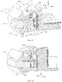
- FIG. 1 is a schematic structural diagram of an electronic device 100 according to an embodiment of this application
- FIG. 2 is a schematic diagram of a partial structure of the electronic device 100 shown in FIG. 1 .
- the electronic device 100 may be a tablet computer, a mobile phone, a camera, a personal computer, a notebook computer, a vehicle-mounted device, a wearable device, AR (Augmented Reality, Augmented Reality) glasses, an AR helmet, VR (Virtual Reality, Virtual Reality) glasses, or a VR helmet.
- a mobile phone is used as an example of the electronic device 100 in the embodiment shown in FIG. 1 for description.
- a width direction of the electronic device 100 is defined as an X axis.
- a length direction of the electronic device 100 is defined as a Y axis.
- a thickness direction of the electronic device 100 is defined as a Z axis.
- the electronic device 100 includes a middle frame 10, a screen 20, a rear cover 30, a main board 40, and a button assembly 50.
- the screen 20 and the rear cover 30 face toward each other and are respectively located on two sides of the middle frame 10.
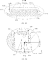
- FIG. 3 is a schematic structural diagram of a middle frame 10 of the electronic device 100 shown in FIG. 2 .
- the middle frame 10 includes an assembly face 101, a mounting face 102 that faces away from the assembly face 101, and an external face 103 that are connected between the assembly face 101 and the mounting face 102.
- the middle frame 10 is provided with a mounting slot 1011 and a button slot 1031.
- the mounting slot 1011 is recessed in a direction from the assembly face 101 to the mounting face 102.
- the mounting slot 1011 includes a slot side wall and a slot bottom wall (not shown in the figure).
- the slot side wall is located on a plane in the Z-axis direction, and the slot bottom wall is located on an X-Y plane.
- the slot side wall includes a first slot wall 1012 and a second slot wall 1013 that face toward each other, and a third slot wall 1014 and a fourth slot wall 1015 that are connected between the first slot wall 1012 and the second slot wall 1013.
- the second slot wall 1013 is a slot wall of the slot side wall away from the external face 103, and the second slot wall 1013 is partially recessed in the X-axis direction to form a clamping slot 1016.
- the clamping slot 1016 includes a clamping slot wall 1016a facing opposite to the assembly face 101, and a clamping slot bottom wall 1016b connected to the clamping slot wall 1016a.
- two clamping slots 1016 are provided.
- the two clamping slots 1016 are respectively a first clamping slot 1016 and a second clamping slot 1016, and the first clamping slot 1016 and the second clamping slot 1016 are provided at an interval in the Y-axis direction.
- the slot bottom wall partially protrudes to form a limiting block (not shown in the figure), and the limiting block extends in the X-axis direction and is connected between the first slot wall 1012 and the second slot wall 1013.
- the limiting block includes a first side face and a second side face that face away from each other. It should be understood that, the mounting slot 1011 is not limited to being strip-shaped as shown in FIG. 3 only, and may alternatively be cylindrical or cuboid.
- buttons slot 1031 An opening of the button slot 1031 is located on the external face 103.
- the button slot 1031 is recessed from the external face 103 in the X-axis direction and communicates with the mounting slot 1011.
- the button slot 1031 includes a button slot bottom wall 1032, and the button slot bottom wall 1032 is partially recessed to form a first mounting hole 1033 and a second mounting hole 1034.
- the first mounting hole 1033 and the second mounting hole 1034 are arranged at an interval in the Y-axis direction and both communicate with the mounting slot 1011.
- the button slot 1031 is not limited to being strip-shaped as shown in FIG. 3 only, and may alternatively be cylindrical or cuboid.
- the middle frame 10 includes a side frame 11 and a middle plate 12.
- the side frame 11 may be made of a metal material.
- the middle plate 12 may be made of a plastic material.
- the middle plate 12 may be formed on the side frame 11 through an injection molding process, so as to form a whole together with the side frame 11, thereby improving overall strength of the middle plate 12 and the side frame 11.
- the screen 20 is mounted on the mounting face 102.
- the screen 20 includes a display face that faces away from the middle frame 10, where the display face is configured to display images, videos, and the like.
- the screen 20 is a 2D (Dimensions, Dimensions) display.
- the screen 20 may alternatively be a 2.5D curved screen or a 3D curved screen.
- the screen 20 includes a cover plate and a display panel fixed to the cover plate.
- the cover plate may be made of glass or another transparent material.
- the display panel may use an LED (Liquid Crystal Display, Liquid Crystal Display), an OLED (Organic Light-Emitting Diode, Organic Light-Emitting Diode) display, an AMOLED (Active-Matrix Organic Light Emitting Diode, Active-Matrix Organic Light Emitting Diode) display, a FLED (Flex Light-Emitting Diode, Flex Light-Emitting Diode) display, a Mini LED, a Micro LED, a Micro OLED, a QLED (Quantum Dot Light Emitting Diode, Quantum Dot Light Emitting Diode), or the like.
- the display panel may also have a touch control function, that is, the display panel is a touch display panel.
- the display panel is electrically connected to the main board 40.
- the display panel can generate a touch control signal and transmit the touch control signal to a processor on the main board 40.
- the processor receives the touch control signal, and controls, based on the touch control signal, an application (Application, App) in the electronic device 100 to be opened.
- the rear cover 30 is located on a side of the middle frame 10 facing away from the screen 20.
- the rear cover 30 faces away from the user, and the screen 20 faces toward the user.
- the rear cover 30 is mounted on the assembly face 101.
- the rear cover 30 may be detachably mounted on the middle frame 10, so as to facilitate maintenance and replacement of a battery, a memory card or a circuit board in the electronic device 100.
- the rear cover 30 may be made of engineering plastic such as PC (Polycarbonate, Polycarbonate) and ABS (Acrylonitrile Butadiene Styrene copolymers, Acrylonitrile Butadiene Styrene copolymers), or metal alloy such as titanium alloy and aluminum magnesium alloy.
- An accommodating space (not shown in the figure) is enclosed by the rear cover 30, the screen 20 and the middle frame 10.
- the accommodating space may be configured to accommodate a microphone, a loudspeaker, a battery, or another device. It may be learned from FIG. 1 that, a roughly cuboid structure is enclosed by the rear cover 30, the screen 20 and the middle frame 10.
- the main board 40 is mounted in the accommodating space.
- a processor (not shown in the figure) and a memory (not shown in the figure) are disposed on the main board 40.
- the memory is configured to store computer program code.
- the computer program code includes a computer instruction.
- the processor is configured to call a computer instruction so as to enable the electronic device 100 to perform a corresponding operation.
- the button assembly 50 is electrically connected to the main board 40.
- the button assembly 50 may be a button for adjusting a volume.
- the button assembly 50 can generate an electric signal and transmit the electric signal to the processor on the main board 40.
- the processor receives the electric signal and adjusts, based on the electric signal, a volume of the electronic device 100.
- the button assembly 50 may alternatively be a power button for waking up or turning off the screen 20, or may be another button mounted on a side face of the electronic device 100. This is not specifically limited in this application.
- the button assembly 50 includes a switch member 51, a pressing member 52 and a fixing member 53.
- the switch member 51 is mounted in the mounting slot 1011 and electrically connected to the main board 40.
- Part of the pressing member 52 is mounted in the mounting slot 1011, and part of the pressing member 52 extends out of the middle frame 10.
- the fixing member 53 is located in the mounting slot 1011 and faces toward the switch member 51.
- the fixing member 53 is configured to fix and limit the switch member 51 and the pressing member 52. It should be learned that, that the switch member 51 is mounted in the mounting slot 1011 means that at least part of the switch member 51 is mounted in the mounting slot 1011.
- the pressing member 52 is configured to apply acting force to the switch member 51, so as enable the switch member 51 to generate an electric signal and transmit the electric signal to the main board 40. For example, when a user presses the pressing member 52, the pressing member 52 moves toward the accommodating space. When pressure is applied to the switch member 51 through the pressing member 52, the switch member 51 generates an electric signal and transmits the electric signal to the main board.
- FIG. 4 is a schematic structural diagram of a switch member 51 of a button assembly 50 shown in FIG. 2
- FIG. 5 is an exploded schematic structural diagram of the switch member 51 shown in FIG. 4 .
- the switch member 51 includes a circuit board 511, a switch 512, and an elastic member 513.
- the switch 512 is fixed to the circuit board 511 and electrically connected to the circuit board 511.
- the elastic member 513 is mounted on a side of the switch 512 facing away from the circuit board 511.
- the circuit board 511 includes a first limiting part 5111 and a second limiting part 5112.
- first limiting parts 5111 are provided, and the two first limiting parts 5111 are located at two ends of the circuit board 511. It should be noted that, in other embodiments, one or two or more first limiting parts 5111 may be provided. This is not specifically limited in this application.
- the circuit board 511 is provided with a first limiting slot 5113, and the first limiting slot 5113 runs through the circuit board 511 in a thickness direction of the circuit board 511.
- the first limiting slot 5113 includes a first limiting slot wall 5113a and a second limiting slot wall 5113b that face toward each other.
- the circuit board 5111 includes a reinforcing plate 5114 and a flexible circuit board 5115, and part of the flexible circuit board 5112 is mounted on the reinforcing plate 5114.
- the reinforcing plate 5114 is of a flat panel-shaped structure and is parallel to a Y-Z plane.
- the reinforcing plate 5114 includes a first mounting face 5115, a second mounting face 5116, and a peripheral face 5117.
- the first mounting face 5115 and the second mounting face 5116 face away from each other and are both parallel to the Y-Z plane.
- the peripheral face 5117 is connected between the first mounting face 5115 and the second mounting face 5116.
- the peripheral face 5117 includes a first peripheral face 5117a, a second peripheral face 5117b, a third peripheral face 5117c, and a fourth peripheral face 5117d that are sequentially connected.
- the first peripheral face 5117a partially protrudes to form a second limiting part 5112, and the second limiting part 5112 protrudes from the first peripheral face 5117a in a forward direction of the Z axis.
- the second limiting part 5112 includes a second limiting face 5112a facing the same direction as the first mounting face 5115.
- the second limiting part 5112 is located in a middle area of the first peripheral face 5117a.
- the second peripheral face 5117b partially protrudes to form one first limiting part 5111, and the first limiting part 5111 protrudes from the second peripheral face 5117b in a reverse direction of the Y axis.
- the first limiting part 5111 is located on an edge area of the second peripheral face 5117b facing away from the first peripheral face 5117a.
- the first limiting part 5111 includes a first limiting face 5111a facing the same direction as the first peripheral face 5117a and a bottom face 5111b facing away from the first limiting face 5111a.
- the third peripheral face 5117c and the bottom face 5111b are located on a same surface. Specifically, the third peripheral face 5117c faces away from the first peripheral face 5117a.
- the third peripheral face 5117c is partially recessed to form a first secondary limiting slot 5113a, that is, the first secondary limiting slot 5113a is recessed in a direction from the third peripheral face 5117c to the first peripheral face 5117a.
- the first secondary limiting slot 5113a is located in a middle area of the third peripheral face 5117c, and runs through the first mounting face 5115 and the second mounting face 5116.
- the fourth peripheral face 5117d faces away from the second peripheral face 5117b.
- the fourth peripheral face 5117d partially protrudes to form another first limiting part 5111, and the first limiting part 5111 protrudes from the fourth peripheral face 5117d in a forward direction of the Y axis.
- the first limiting part 5111 is located on an area of the fourth peripheral face 5117d facing away from the first peripheral face 5117a.
- the reinforcing plate 5114 is of a symmetrical structure. That is, the reinforcing plate 5114 has a symmetry plane O, and the reinforcing plate 5114 is located on two sides of the symmetry plane O and symmetrical about the symmetry plane O, so as to simplify a preparation process of the reinforcing plate 5114.
- the second limiting part 5112 is located right in the middle of the first peripheral face 5117a and is symmetrical about the symmetry plane O.
- the two first limiting parts 5111 are symmetrical about the symmetry plane O.
- the first secondary limiting slot 5113a is located right in the middle of the third peripheral face 5117a and is symmetrical about the symmetry plane O.
- the reinforcing plate 5114 is made of a metal material such as steel or a high-strength plastic material.
- the flexible circuit board 5115 includes a first section 5115a, a second section 5115b, and a third section 5115c.
- the first section 5115a is provided with a second secondary limiting slot 5113b, and the second secondary limiting slot 5113b runs through a first end 511a in a thickness direction of the first end 511a.
- the first section 5115a is mounted on the first mounting face 5115 of the reinforcing plate 5114.
- the first limiting part 5111, the second limiting part 5112, and the first secondary limiting slot 5113a are exposed.
- the second secondary limiting slot 5113b and the first secondary limiting slot 5113a jointly form the first limiting slot 5113.
- the first section 5115a is mounted on the first mounting face 5115 through a first bonding layer 61.
- the first section 5115a as a flexible circuit board is extremely prone to folding damage in use, and the first section 5115a mounted on the first mounting face 5115 increases mechanical strength of the first section 5115a and increases assembly and use convenience of the first section 5115a.
- the second section 5115b and the first section 5115a are disposed at an interval.
- the second section 5115b is located on a side of the reinforcing plate 5114 away from the first section 5115a.
- the second section 5115b is mounted in a whole-machine inner cavity and electrically connected to the main board.
- the third section 5115c is connected between the first section 5115a and the second section 5115b.
- the third section 5115c is a bent section.
- the bent third section 5115c connected between the first section 5115a and the second section 5115b can not only improve mounting flexibility of the flexible circuit board 5115 to prevent the flexible circuit board 5115 from being interfered with by the middle frame 10, but also transmit, to the main board sequentially through the third section 5115c and the second section 5115b, an electric signal that is transmitted to the first section 5115a.
- two switches 512 are provided.
- the two switches 512 are both mounted on a surface of the flexible circuit board 5115 facing away from the fixing plate 5114 and electrically connected to the flexible circuit board 5115.
- the two switches 512 are respectively a first switch 512 and a second switch 512.
- the first switch 512 and the second switch 512 are mounted on a surface of the first section 5115a facing away from the fixing plate 5114 at an interval in the Y-axis direction and both electrically connected to the first section 5115a.
- the electric signal generated by the triggered first switch 512 or the triggered second switch 512 is transmitted to the main board sequentially through the first section 5115a, the third section 5115c, and the second section 5115b to be used to control a volume of the electronic device 100. It should be noted that, in other embodiments, one or two or more switches 512 may be provided. This is not specifically limited in this application.
- two elastic members 513 are provided.
- the two elastic member 513 are mounted on a side of the two switches 512 facing away from the flexible circuit board 5115.
- the two elastic members 513 are respectively a first elastic member 513 and a second elastic member 513.
- the first elastic member 513 covers the first switch 512
- the second elastic member 513 covers the second switch 512. That is, the first elastic member 513 and the second elastic member 513 respectively cover the first switch 512 and the second switch 512, so as to effectively protect the first switch 512 and the second switch 512 and prevent the first switch 512 and the second switch 512 from collision damage by other parts.
- the first elastic member 513 includes a middle part 5131 and an edge part 5132 surrounding the middle part 5131.
- the middle part 5131 directly faces toward the first switch 512.
- the edge part 5132 extends in a direction from the middle part 5131 to the first switch 512 and forms a compression space together with the middle part 5131, that is, the first elastic member 513 is substantially of a cover body structure and covers the first switch 512 within the compression space.
- the middle part 5131 moves toward the first switch 512 and drives the edge part 5132 to be bent toward the first switch 512 so as to squeeze the compression space until the middle part 5131 abuts against the first switch 512 to enable the first switch 512 to generate an electric signal.
- the middle part 5131 and the edge part 5132 both restore an original state under the action of elastic force of their own, and in this case, the compression space restores an original state.
- the second elastic member 513 and the first elastic member 513 substantially have a same structure. Details are not described herein again.
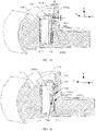
- FIG. 6 is a schematic cross-sectional view of an internal structure of the electronic device 100 shown in FIG. 2 in a direction A-A
- FIG. 7 is an enlarged schematic structural diagram of an area B of the structure shown in FIG. 6 .
- part of the circuit board 511, the first switch 512, the second switch 512, the first elastic member 513, and the second elastic member 513 are all located in the mounting slot 1011.
- the circuit board 511 is fixedly connected to the second slot wall 1013.
- the reinforcing plate 5114 is mounted on the first slot wall 1012 through a second bonding layer 62.
- the first section 5115a, the first switch 512, the second switch 512, the first elastic member 513, and the second elastic member 513 are all mounted on a side of the reinforcing plate 5114 facing away from the second bonding layer 62.
- a limiting block 1018 on the slot bottom wall 1017 of the mounting slot 1011 is clamped in the first limiting slot 5113, so as to limit the circuit board 511 to move in the Y-axis direction and limit the circuit board 511 in the Y-axis direction. That the limiting block 1018 is clamped in the first limiting slot 5113 means that at least part of the limiting block 1018 is clamped in the first limiting slot 5113.
- circuit board 511 due to tolerance of the circuit board 511 and the limiting block 1018 during production or assembly, provided that a distance d1 between the first side face 1018a of the limiting block 1018 and the first limiting slot wall 5113a less than or equal to 0.1 mm and a distance d2 between the second side face 1018b and the second limiting slot wall 5113b less than or equal to 0.1 mm, it may be considered that the circuit board 511 is effectively limited in the Y-axis direction.
- the first switch 512, the second switch 512, the first elastic member 513, and the second elastic member 513 are all located on a side of the first section 5115a facing away from the reinforcing plate 5114.
- the third section 5115c is located on the assembly face 101.
- the assembly face 101 may be partially recessed to form an accommodating slot (not shown in the figure), and the accommodating slot accommodates the third section 5115c, so as to limit the third section 5115c to move in the Y-axis direction and limit the second section 5115b in the Y-axis direction.
- the second section is mounted in a whole-machine inner cavity and electrically connected to the main board. It should be understood that, a mounting manner of the second section in the whole-machine inner cavity is substantially the same as a mounting manner of the first section 5115a in the mounting slot 1011. Details are not described herein again.
- FIG. 8 is an exploded schematic structural diagram of a pressing member 52 of a button assembly 50 shown in FIG. 2
- FIG. 9 is a schematic cross-sectional view of an internal structure of the electronic device 100 shown in FIG. 2 in a direction C-C.
- the pressing member 52 includes a button 521 and an elastic sleeve 522.
- the button 521 includes a pressing part 5211, and a pushing part 5212 and a clamping part 5213 that are connected to the pressing part 5211, where the pushing part 5212 and the clamping part 5213 are located on a same side of the pressing part 5211.
- the pressing part 5211 is partially exposed out of the external face 103 of the middle frame 10.
- the pressing part 5211 includes a pressing end part 5214, where the pressing end part 5214 is exposed out of the external face 103 of the middle frame 10, and the rest part of the pressing part 5211 is located in the button slot 1031.
- the pushing part 5212 is located on a side of the pressing part 5211 facing away from the pressing end face 5214.
- the pushing part 5212 extends from the button slot 1031 into the mounting slot 1011, and the pushing part 5212 faces toward the switch 512.
- two pushing parts 5212 are provided.
- the two pushing parts 5212 are respectively a first pushing part 5212 and a second pushing part 5212.
- the first pushing part 5212 passes through the first mounting hole 1033 from the button slot 1031 and extends into the mounting slot 1011, and the first pushing part 5212 faces toward the first switch 512.
- the first pushing part 5212 includes a pushing end part 5215 away from the pressing part 5211, where the pushing end part 5215 directly faces toward the first switch 512, that is, the pushing end part 5215 directly faces toward the middle part 5131.
- the second pushing part 5212 and the first pushing part 5212 are arranged at an interval in the Y-axis direction. It should be understood that, an assembly manner of the second pushing part 5212 is the same as an assembly manner of the first pushing part 5212.
- the second pushing part 5212 passes through the second mounting hole from the button slot 1031 and extends into the mounting slot 1011, and the second pushing part 5212 faces toward the second switch 512. It should be noted that, that the pushing part 5212 faces toward the switch 512 means that at least part of the pushing part 5212 directly faces toward the first switch 512, and in this case, the pushing part 5212 can apply acting force to the switch 512.
- first pushing part 5212, the second pushing part 5212 and the pressing part 5211 are integrally molded.
- first pushing part 5212, the second pushing part 5212 and the pressing part 5211 may alternatively be fixed in a fixing manner of welding or gluing. This is not specifically limited in this application.
- the elastic sleeve 522 sleeves an outer surface of the pushing part 5212.
- two elastic sleeves 522 are provided.
- the two elastic sleeves 522 are respectively a first elastic sleeve 522 and a second elastic sleeve 522.
- the first elastic sleeve 522 sleeves an outer surface of the pushing end part 5215 of the first pushing part 5212
- the second elastic sleeve 522 sleeves an outer surface of the pushing end part 5215 of the second pushing part 5212, so as to buffer pressure applied by the pushing part 5212 to the middle part 5131. This prevents the elastic member 513 from damage by excessively large pressure and prolongs a service life of the elastic member 513.
- the pressing part 5211 pushes the first pushing part 5212 to move toward the middle part 5131, and in this case, the first pushing part 5212 drives the first elastic sleeve 522 to move toward the middle part 5131 until the pushing end part 5217 of the first pushing part 5213 applies acting force to the middle part 5131 through the first elastic sleeve 522, so as to enable the first switch 512 to generate an electric signal and transmit the electric signal to the main board 40.
- the first switch 512 can apply external force to the middle part 5214 under the action of elastic force of its own and then apply external force to the pushing end part 5215 through the first elastic sleeve 522 to enable the first pushing part 5212 to return to an original position, so as to cut off electrical connection of the first switch 512.
- the first elastic sleeve 522 and the middle part 5131 may always be in a contact state, or a gap may exist between the first elastic sleeve 522 and a middle 5141. It may be understood that, a switching process of the second switch 512 is substantially the same as a switching process of the first switch 512. Details are not described herein again.
- FIG. 10 is a schematic cross-sectional view of an internal structure of the electronic device 100 shown in FIG. 2 in a direction D-D.
- the clamping part 5213 extends from the button slot 1031 into the mounting slot 1011.
- two clamping parts 5213 are provided.
- the two clamping parts 5213 are respectively connected to two ends of the pressing part 5211.
- the two clamping parts 5213 are respectively a first clamping part 5213 and a second clamping part 5213.
- the first clamping part 5213 is located on a side of the first pushing part 5212 facing away from the second pushing part 5212 and connected to the first pushing part 5212.
- the first clamping part 5213 penetrates through the first mounting hole 1033 from the button slot 1031 and extends into the mounting slot 1011.
- the first clamping part 5213 includes a first part 5216, a second part 5217, and a third part 5218.
- the first part 5216 is connected between the pressing part 5211 and the second part 5217.
- the second part 5217 is connected between the first part 5216 and the third part 5218.
- the third part 5218 extends in a direction leaving the second clamping part 5213.
- a clamping slot 5213d is formed among the first part 5216, the second part 5217 and the third part 5218.
- the second clamping part 5213 is located on a side of the second pushing part 5212 facing away from the first pushing part 5212 and connected to the second pushing part 5212. It may be understood that, the second clamping part 5213 and the first clamping part 5213 substantially have a same structure. Details are not described herein again.
- the first clamping part 5213, the second clamping part 5213, and the pressing part 5211 are integrally molded. Certainly, in other embodiments, the first clamping part 5213, the second clamping part 5213 and the pressing part may alternatively be fixed in a fixing manner of welding or gluing. This is not specifically limited in this application.
- FIG. 11 is a schematic structural diagram of a fixing member 53 of a button assembly 50 shown in FIG. 2
- FIG. 12 is a schematic cross-sectional view of an internal structure of the electronic device 100 shown in FIG. 2 in a direction E-E.
- the fixing member 53 includes a first end face 53a and a second end face 53b that face away from each other.
- the first end face 53a faces toward or abuts against the third slot side wall 1014
- the second end face 53b faces toward or abuts against the fourth slot side wall 1015, so as to limit the fixing member 53 to move in the Y-axis direction and limit the fixing member 53 in the Y-axis direction.
- the fixing member 53 includes a fixing plate 531, an engaging plate 532, a first connecting plate 533, a first stop plate 534, a lug 535, a second connecting plate 536, and a second stop plate 537.
- the fixing plate 531 is provided with a second limiting slot 5315, and the second limiting slot 5315 runs through the fixing plate 531 in a thickness direction of the fixing plate 531.
- the fixing plate 531 includes a first surface 5311 and a second surface 5312 that face away from each other, and an upper end face 5313 and a first lower end face 5314 that are connected between the first surface 5311 and the second surface 5312.
- the first surface 5311 is a surface of the fixing plate 531 facing toward the circuit board 511. That is, the second surface 5312 is a surface of the fixing plate 531 facing away from the circuit board 511.
- the upper end face 5313 faces away from the first lower end face 5314.
- An opening of the second limiting slot 5315 is located on the first lower end face 5314 and recessed in a direction from the first lower end face 5314 to the upper end face 5315. Specifically, the opening of the second limiting slot 5315 is located in a middle area of the first lower end face 5314 and runs through the first surface 5311 and the second surface 5312.
- the second limiting slot 5315 includes a third limiting slot wall 5315a and a fourth limiting slot wall 5315b that face toward each other.
- the engaging plate 532 is connected to the fixing plate 531.
- two engaging plates 532 are provided.
- the two engaging plates 532 are respectively a first engaging plate 532 and a second engaging plate 532.
- a first assembly slot 5316 is enclosed by the first engaging plate 532 and the fixing plate 531
- a second assembly slot 5317 is enclosed by the second engaging plate 632 and the fixing plate 531.
- the fixing plate 531 is fixedly connected to the slot side wall.
- the fixing plate 531 is fixedly connected to the first slot wall 1012.
- the fixing plate 531 is mounted on the first slot wall 1012 through a third bonding layer (not shown in the figure), that is, the third bonding layer is connected between the second surface 5312 and the first slot wall 1012.
- the fixing plate 531 may alternatively be fixedly connected to the slot bottom wall 1017.
- FIG. 13 is an enlarged schematic structural diagram of an area F of the structure shown in FIG. 12 .
- the limiting block 1018 on the slot bottom wall 1017 is clamped in the second limiting slot 5315, so as to limit the fixing plate 531 to move in the Y-axis direction and limit the fixing plate 531 in the Y-axis direction. It should be learned that, due to tolerance of the second limiting slot 5315 and the limiting block 1018 during production or assembly, provided that a distance d5 between the first side face 1018a of the limiting block 1018 and the third limiting slot wall 5315a of the second limiting slot 5315 less than or equal to 0.1 mm and a distance d6 between the second side face 1018b and the fourth limiting slot wall 5315b of the second limiting slot 5315 less than or equal to 0.1 mm, it may be considered that the fixing plate 531 is effectively limited in the Y-axis direction.
- the engaging plate 532 clamps the clamping part 5313.
- the first clamping part 5213 sequentially penetrates through the first mounting hole 1033 and the first assembly slot 5316 from the button slot and extends into the mounting slot 1011
- the second clamping part 5213 sequentially penetrates through the second mounting hole 1034 and the second assembly slot 5317 from the button slot and extends into the mounting slot 1011
- part of the first engaging plate 532 is clamped in the clamping slot 5213d of the first clamping part 5213
- part of the second engaging plate 532 is clamped in the clamping slot 5213d of the second clamping part 5213, so as to fix the pressing member 52 to the middle frame 10.
- the first connecting plate 533 is connected to the fixing plate 531.
- two first connecting plates 533 are provided.
- the two first connecting plates 533 are respectively connected to two ends of the fixing plate 531 and are bent and extend in a direction from the fixing plate 531 to a side of the fixing plate 531 facing toward the first surface 5311.
- Two faces of the two first connecting plates 533 facing away from each other are respectively a first end face 53a and a second end face 53b.
- the first stop plate 534 is connected to the fixing plate 531.
- the first stop plate 534 is connected to the fixing plate 531 through the first connecting plate 533, that is, the first connecting plate 533 is connected between the first stop plate 534 and the fixing plate 531.
- two first stop plates 534 are provided. Each of the first stop plates 534 extends from one first connecting plate 533 to the other first connecting plate 533 and is spaced from the fixing plate 531.
- the first stop plate 534 is located on a side of the first limiting part 5111 away from the slot bottom wall 1017 of the mounting slot 1011, and the first stop plate 534 faces toward the first limiting part 5111 or abuts against the first limiting part 5111, so as to limit the first limiting part 5111 to move in the Z-axis direction and effectively limit the first limiting part 5111 in the Z-axis direction. That the first stop plate 534 faces toward the first limiting part 5111 or abuts against the first limiting part 5111 means that at least part of the first stop plate 534 directly faces toward the first limiting part 5111 or at least part abuts against the first limiting part 5111.
- FIG. 14 is an enlarged schematic structural diagram of an area G of the structure shown in FIG. 6 .
- the first stop plate 534 includes a second lower end face 5341 facing the same direction as the first lower end face 5314, a side end face 5342 away from the first connecting plate 533, a third surface 5343 facing the same direction as the first surface 5311, and a fourth surface 5344 facing away from the third surface 5343.
- the first stop plate 534 has effectively limited the first limiting part 5111 in the Z-axis direction.
- FIG. 15 is a schematic cross-sectional view of an internal structure of the electronic device 100 shown in FIG. 2 in a direction H-H.
- the first stop plate 534 partially protrudes to form a clamping protrusion 5347, and the clamping protrusion 5347 is embedded in the clamping slot 1016.
- the clamping protrusion 5347 protrudes in a direction from the fourth surface 5344 to the first surface 5343.
- the clamping protrusion 5347 includes an upper side face 5348 facing the same direction as the upper end face 5313, and a top face 5349 facing away from the fixing plate 531.
- the clamping protrusion 5347 is clamped in the clamping slot 1016, so as to limit the first stop plate 534 to move in the Z-axis direction, further limit the first limiting part 5111 to move in the Z-axis direction and effectively limit the first limiting part 5111 in the Z-axis direction.
- a distance d8 between the top face 5349 and the clamping slot bottom wall 1016b is equal to or greater than 0.05 mm.
- the first clamping slot 1016 is considered as effectively clamping the clamping protrusion 5347 in the Z-axis direction.
- the two first stop plates 534 simultaneously limit the two first limiting parts 5111 to move in the Z-axis direction, that is, limit the reinforcing plate 5114 to move in the Z-axis direction, so as to effectively limit the reinforcing plate 5114 in the Z-axis direction,
- the pressing member 51 does not fall off the mounting slot 1011 easily. This ensures long-term effectiveness of the button assembly 50 and improves user experience.
- the lug 535 is connected to the first stop plate 534. Specifically, the lug 535 is connected to an end of the first stop plate 534 facing away from the second lower end face 5341 and is bent and extends in a direction from the first stop plate 534 to the fixing plate 531. In this embodiment, two lugs 535 are provided, and the two lugs 535 are respectively connected to the two first stop plates 534, so as to facilitate mounting or demounting of the fixing member 53.
- the two lugs 535 may be pressed to mount the fixing member 53 in the mounting slot 1011; and during demounting of the fixing member 53, the two lugs 535 may be lifted by using a tool such as tweezers to take the fixing member 53 out of the mounting slot 1011.
- the lug 535 may alternatively be connected to the fixing plate 531 and be bent and extend from the fixing plate 531 in a direction leaving the first slot side wall 1012. This is not specifically limited in this embodiment.
- FIG. 16 is a schematic cross-sectional view of an internal structure of the electronic device 100 shown in FIG. 2 in a direction H-H according to another implementation.
- the electronic device 100 shown in this implementation differs from the fixing member electronic device 100 shown in the foregoing implementation in that, the first stop plate 534 partially protrudes to form a limiting protrusion 53410, the limiting protrusion 53410 includes an end face 53411 facing toward the slot bottom wall 1017 of the mounting slot 1011, and the end face 53411 faces toward the first limiting part 5111 or abuts against the first limiting part 5111, so as to limit the first limiting part 5111 to move in the Z-axis direction and effectively limit the first limiting part 5111 in the Z-axis direction.
- the limiting protrusion 53410 protrudes in a direction from the third surface 5343 to the fourth surface 5344, so as to increase a limiting width of the first stop plate 534 capable of limiting the second limiting part 5114.
- the first stop plate 534 can still limit the first limiting part 5111 to move in the Z-axis direction, so as to effectively limit the first limiting part 5111, so that the reinforcing plate 5114 does not fall off the mounting slot 1011 easily. This improves use reliability of the button assembly 50.
- the limiting protrusion 53410 has effectively positioned the first limiting part 5111 in the Z-axis direction.
- FIG. 17 is a schematic cross-sectional view of an internal structure of the electronic device 100 shown in FIG. 2 in a direction H-H according to a third implementation.
- the electronic device 100 shown in this implementation differs from the electronic device 100 shown in the foregoing two implementations in that, a periphery of the first stop plate 534 is bent and extends to form a limiting plate 538.
- the limiting plate 538 includes a limiting face 5381 facing toward the slot bottom wall 1017 of the mounting slot 1011, and the limiting face 5381 faces toward the first limiting part 5111 or abuts against the first limiting part 5111, so as to limit the first limiting part 5111 to move in the Z-axis direction and limit the first limiting part 5111 in the Z-axis direction.
- an end of the first stop plate 534 facing toward the slot bottom wall 1017 of the mounting slot 1011 is bent in the Y-axis direction and then extends toward the fixing plate 531 to form the limiting plate 538, so as to increase a limiting width of the first stop plate 534 capable of limiting the first limiting part 5111.
- the first stop plate 534 can still limit the first limiting part 5111 to move in the Z-axis direction, so as to effectively limit the first limiting part 5111, so that the reinforcing plate 5114 does not fall off the mounting slot 1011 easily. This improves use reliability of the button assembly 50.
- the limiting plate 538 has effectively positioned the first limiting part 5111 in the Z-axis direction.
- FIG. 18 is a schematic cross-sectional view of an internal structure of the electronic device 100 shown in FIG. 2 in a direction H-H according to a fourth implementation.
- the electronic device 100 shown in this implementation differs from the electronic device 100 shown in the foregoing third implementation in that, an end of the first stop plate 534 away from the first connecting plate 533 is bent in the Z-axis direction and then extends toward the fixing plate 531 to form the limiting plate 538, so as to increase a limiting width of the first stop plate 534 capable of limiting the first limiting part 5111.
- the first stop plate 534 can still limit the first limiting part 5111 to move in the Z-axis direction, so as to effectively limit the first limiting part 5111, so that the reinforcing plate 5114 does not fall off the mounting slot 1011 easily. This improves use reliability of the button assembly 50.
- the limiting plate 538 has effectively positioned the first limiting part 5111 in the Z-axis direction.
- FIG. 19 is a schematic cross-sectional view of an internal structure of the electronic device 100 shown in FIG. 2 in a direction H-H according to a fifth implementation.
- the electronic device 100 shown in this implementation differs from the electronic device 100 shown in the foregoing fourth implementation in that, the fixing member 53 further includes an auxiliary connecting plate 539, where the auxiliary connecting plate 539 is connected to the fixing plate 531.
- the fixing member 53 further includes an auxiliary connecting plate 539, where the auxiliary connecting plate 539 is connected to the fixing plate 531.
- two auxiliary connecting plates 539 are provided, and the two auxiliary connecting plates 539 are both connected to the upper end face of the fixing plate 531 and extend in a direction from the fixing plate 531 to a side of the fixing plate 531 facing toward the first surface 5311.
- Each of the auxiliary connecting plates 539 is connected between one first stop plate 534 and the fixing plate 531.
- FIG. 20 is a schematic cross-sectional view of an internal structure of the electronic device 100 shown in FIG. 2 in a direction I-I
- FIG. 21 is an enlarged schematic structural diagram of an area J of the structure shown in FIG. 20 .
- the second connecting plate 536 is connected to the fixing plate 531.
- the second connecting plate 536 is connected to the upper end face 5313 of the fixing plate 531 and extends from the fixing plate 531 to the side on which the first stop plate 534 is located.
- the second stop plate 537 is connected to the fixing plate 531 and is spaced from and faces toward the fixing plate 531.
- the second stop plate 537 is connected to the fixing plate 531 through the second connecting plate 536, that is, the second connecting plate 536 is connected between the fixing plate 531 and the second stop plate 537.
- the second stop plate 537 partially protrudes to form a protrusion 5371.
- the second stop plate 537 includes a fifth surface 5372 facing away from the fixing plate 531 and a sixth surface 5373 facing away from the fifth surface 5372, and the protrusion 5371 protrudes in a direction from the sixth surface 5373 to the fifth surface 5372.
- the second connecting plate 536 and the second stop plate 537 are both located in the mounting slot 1011 and located on a side of the fixing plate 531 facing away from the third bonding layer 63.
- the second stop plate 537 is located on a side of the second limiting part 5112 facing away from the second slot side wall 1013, and the second stop plate 537 faces toward the second limiting part 5112 or abuts against the second limiting part 5112, so as to limit the second limiting part 5112 to move in the X-axis direction, that is, limit the reinforcing plate 5114 to move in the X-axis direction and limit the reinforcing plate 5114 in the X-axis direction.
- the protrusion 5371 abuts against the first limiting face 5114b, to compensate for errors caused by tolerance of the second stop plate 537 and the reinforcing plate 5114 during production and assembly, so as to effectively limit the reinforcing plate 5114 in the X-axis direction.
- the second stop plate 537 and the second limiting part 5112 due to tolerance of the second stop plate 537 and the second limiting part 5112 during production or assembly, provided that a distance between two faces of the second stop plate 537 and the second limiting part 5112 that face toward each other less than or equal to 0.1 mm, that is, a distance d10 between the fifth surface 5372 of the second stop plate 537 and the second limiting face 5112a of the second limiting part 5112 less than or equal to 0.1 mm, it may be considered that the second stop plate 537 has effectively limited the second limiting part 5112 in the X-axis direction.
- the fixing plate 531, the engaging plate 532, the first connecting plate 533, the first stop plate 534, the lug 535, the second connecting plate 536, and the second stop plate 537 are of an integrally molded structure.
- the fixing member 53 is made of steel.
- the fixing member 53 may be formed with a steel plate through a stamping process. This improves overall strength of the fixing member 53.
- the electronic device 100 shown in this embodiment uses the first limiting plate 533 to limit the reinforcing plate 5114 in the X-axis direction, uses the limiting block 1018 to limit the reinforcing plate 5114 in the Y-axis direction, and uses the first stop plate 534 and the third limiting plate 537 to limit the reinforcing plate 533 in the Z-axis direction.
- the reinforcing plate 5114 limited in the three directions of X, Y and Z does not fall off the mounting slot 1011 easily to cause failure of the button assembly 50. This improves assembly stability of the button assembly 50 in the electronic device 100, ensures long-term use reliability of the button assembly, and improves user experience.
Landscapes
- Engineering & Computer Science (AREA)
- Computer Hardware Design (AREA)
- Theoretical Computer Science (AREA)
- General Engineering & Computer Science (AREA)
- Human Computer Interaction (AREA)
- Physics & Mathematics (AREA)
- General Physics & Mathematics (AREA)
- Microelectronics & Electronic Packaging (AREA)
- Signal Processing (AREA)
- Telephone Set Structure (AREA)
Abstract
Description
- This application claims priority to
Chinese Patent Application No. 201911172810.4, filed with China National Intellectual Property Administration on November 26, 2019 - The present invention relates to the field of electronic device technologies, and in particular, to an electronic device.
- Buttons are common parts for inputting information and instructions and switching states in electronic devices. Therefore, effectiveness of buttons becomes the most basic key point to be considered during design of button structures. However, existing button structures are simply fixed in electronic devices, the button structures are not stable, and after long-term use of the electronic devices, buttons are quite prone to failure, which affects user experience.
- This application provides an electronic device, to improve assembly stability of buttons in the electronic device, ensure long-term use effectiveness of the buttons, and improve user experience.
- The electronic device provided in this application includes a middle frame, a switch member, a pressing member, and a fixing member, where the middle frame includes an external face and an assembly face connected to the external face, the middle frame is provided with a mounting slot and a button slot, an opening of the mounting slot is located on the assembly face, an opening of the button slot is located on the external face, and the button slot communicates with the mounting slot;
the switch member is mounted in the mounting slot, the switch member includes a circuit board and a switch fixed to the circuit board, and the circuit board includes a first limiting part; the pressing member includes a pressing part, and a pushing part and a clamping part that are connected to the pressing part, the pushing part and the clamping part extend from the button slot into the mounting slot, the pushing part faces toward the switch, and the pressing part is partially exposed on the external face of the middle frame; and the fixing member is located in the mounting slot, the fixing member includes a fixing plate, and an engaging plate and a first stop plate that are connected to the fixing plate, the fixing plate is fixedly connected to a slot bottom wall and/or a slot side wall of the mounting slot, the engaging plate clamps the clamping part, the first stop plate is located on a side of the first limiting part away from the slot bottom wall of the mounting slot, and the first stop plate faces toward the first limiting part or abuts against the first limiting part. - In the electronic device shown in this application, the first stop plate of the fixing member faces toward the first limiting part or abuts against the first limiting part. When the electronic device is used for a long time or drops by accident, the first stop plate limits the first limiting part to move in a direction leaving the slot bottom wall of the mounting slot, so that the switch member is always limited in the mounting slot and does not fall off the mounting slot easily. This improves assembly stability of the switch member in the electronic device. When a user presses the pushing part, the pushing part can always abut against the switch of the switch member to trigger the switch. This ensures effectiveness of each press on the pushing part by the user and improves user experience.
- That the pushing part faces toward the switch means that at least part of the pushing part directly faces toward the switch.
- That the first stop plate faces toward the first limiting part means that at least part of the first stop plate directly faces toward the first limiting part, so as to limit the first limiting part to move in a direction leaving the slot bottom wall of the mounting slot.
- In an implementation, the circuit board includes a reinforcing plate and a flexible circuit board, the reinforcing plate includes the first limiting part, the circuit board is mounted on a surface of the reinforcing plate, and the first limiting part is exposed.
- In an implementation, the mounting slot is recessed from the assembly face in a Z-axis direction, the first stop plate limits the first limiting part to move in the Z-axis direction, that is, the fixing member limits the first limiting part in the Z-axis direction through the first stop plate. The Z-axis direction is a thickness direction of the electronic device.
- In an implementation, a distance between two faces of the first stop plate and the first limiting part that face toward each other is less than or equal to 0.1 mm.
- It may be understood that, due to tolerance of the first stop plate and the first limiting part during production or assembly, in this implementation, provided that the distance between the two faces of the first stop plate and the first limiting part that face toward each other less than or equal to 0.1 mm, it may be considered that the first stop plate has effectively limited the first limiting part in the Z-axis direction.
- In an implementation, the slot side wall of the mounting slot includes a first slot side wall and a second slot side wall that face toward each other, where the fixing plate is fixedly connected to the first slot side wall, the second slot side wall is partially recessed to form a clamping slot, the first stop plate partially protrudes to form a clamping protrusion, and the clamping protrusion is embedded in the clamping slot, so as to limit the first stop plate to move in a direction leaving the slot bottom wall of the mounting slot to enable the first stop plate to always face toward or abut against the first limiting part, and limit the first limiting part to move in a direction leaving the slot bottom wall of the mounting slot to limit the first limiting part in the mounting slot. This improves assembly stability of the switch member in the mounting slot and prevents the first limiting part from falling off the mounting slot.
- In an implementation, the first stop plate partially protrudes to form a limiting protrusion, the limiting protrusion includes an end face facing toward the slot bottom wall of the mounting slot, and the end face faces toward the first limiting part or abuts against the first limiting part, so as to increase a limiting width of the first stop plate on the first limiting part. When the first limiting part moves in a direction leaving the second slot side wall, the limiting protrusion can still limit the first limiting part to move in a direction leaving a slot bottom face of the mounting slot, so that the first limiting part is always limited in the mounting slot. This improves assembly stability of the switch member in the mounting slot and prevents the switch member from falling off the mounting slot.
- The limiting protrusion protrudes from the first stop plate in a direction leaving the second slot side wall.
- That the end face of the limiting protrusion faces toward the first limiting part means that at least part of the end face of the limiting protrusion directly faces toward the first limiting part, and that the end face of the limiting protrusion abuts against the first limiting part means that the end face of the limiting protrusion is in contact with the first limiting part, so as to limit the first limiting part to move in a direction leaving the slot bottom wall of the mounting slot.
- In an implementation, a periphery of the first stop plate is bent and extends to form a limiting plate, the limiting plate includes a limiting face facing toward the slot bottom wall of the mounting slot, and the limiting face faces toward the first limiting part or abuts against the first limiting part, so as to increase a limiting width of the first stop plate on a first limiting plate. When the first limiting part moves in a direction leaving the second slot side wall, the limiting plate can still limit the first limiting part to move in a direction leaving a slot bottom face of the mounting slot, so that the first limiting part is always limited in the mounting slot. This improves assembly stability of the switch member in the mounting slot and prevents the switch member from falling off the mounting slot.
- In an implementation, the slot side wall of the mounting slot further includes a third slot side wall and a fourth slot side wall that are connected between the first slot side wall and the second slot side wall, the fixing member includes a first end face and a second end face that face away from each other, and the first end face faces toward or abuts against the third slot side wall, and the second end face faces toward or abuts against the fourth slot side wall, so as to limit the fixing member to move in a direction from the third slot side wall to the fourth slot side wall. This improves assembly stability of the fixing member in the mounting slot.
- In an implementation, a distance between the first end face and the third slot side wall is less than or equal to 0.1 mm, and a distance between the second end face and the fourth slot side wall is less than or equal to 0.1 mm.
- It may be understood that, due to tolerance of the fixing member and the mounting slot during production or assembly, in this implementation, provided that the distance between the first end face and the third slot side wall less than or equal to 0.1 mm and the distance between the second end face and the fourth slot side wall less than or equal to 0.1 mm, it may be considered that the mounting slot has effectively limited the fixing member in the direction from the third slot side wall to the fourth slot side wall.
- In an implementation, the circuit board is fixedly connected to the second slot side wall, the circuit board further includes a second limiting part, the fixing member further includes a second stop plate connected to the fixing plate, the second stop plate is located on a side of the second limiting part away from the second slot side wall, and the second stop plate faces toward the second limiting part or abuts against the second limiting part, so as to limit the second limiting part to move toward the first slot side wall. This improves assembly stability of the switch member in the mounting slot.
- In an implementation, a direction from the second slot side wall to the first slot side wall is an X-axis direction of the electronic device, the second stop plate limits the second limiting part to move toward the first slot side wall, that is, limits the second limiting part to move in the X-axis direction, and that is, the fixing plate limits the second limiting part in the X-axis direction through the second stop plate. The X-axis direction is a width direction of the electronic device.
- In an implementation, a distance between two faces of a second limiting plate and the second limiting part that face toward each other is less than or equal to 0.1 mm.
- It may be understood that, due to tolerance of the second limiting plate and the second limiting part during production or assembly, in this implementation, provided that the distance between the two faces of the second limiting plate and the second limiting part that face toward each other less than or equal to 0.1 mm, it may be considered that the second limiting plate has effectively limited the second limiting part in the X-axis direction.
- In an implementation, the second stop plate partially protrudes to form a protrusion, and the protrusion abuts against a second limited face, so as to compensate for the tolerance of the second limiting plate and the second limiting part during production or assembly. This ensures that the second limiting plate effectively limits the second limiting part in the X-axis direction.
- In an implementation, the fixing member further includes a lug, where the lug is connected to the fixing plate and is bent and extends from the fixing plate in a direction leaving the first slot side wall, or the lug is connected to the first stop plate and is bent and extends from the first stop plate in a direction approaching the fixing plate. During mounting of the fixing member, the lug may be pressed to mount the fixing member in the mounting slot; in addition, during demounting of the fixing member, the lug may be lifted to take the fixing member out of the mounting slot. That is, arrangement of the lug facilitates mounting and demounting of the fixing member.
- In an implementation, the circuit board is provided with a first limiting slot, the first limiting slot runs through the circuit board in a thickness direction of the circuit board, the slot bottom wall of the mounting slot partially protrudes to form a limiting block, and the limiting block is clamped in the first limiting slot, to limit the circuit board to move, so as to effectively limit the circuit board.
- In an implementation, the limiting block is connected between the first slot side wall and the second slot side wall, and the limiting block is clamped in the limiting block, so as to limit the circuit board to move in the direction from the third slot side wall to the fourth slot side wall.
- In an implementation, the direction from the third slot side wall to the fourth slot side wall is a Y-axis direction of the electronic device, the limiting block limits the circuit board to move in the direction from the third slot side wall to the fourth slot side wall, that is, limits the circuit board to move in the Y-axis direction, and that is, limits the circuit board in the Y-axis direction. The Y-axis direction is a length direction of the electronic device.
- In an implementation, the fixing plate is provided with a second limiting slot, the second limiting slot runs through the fixing plate in a thickness direction of the fixing plate, and the limiting block is clamped in the second limiting slot, so as to limit the fixing plate to move in the direction from the third slot side wall to the fourth slot side wall, that is, limit the fixing plate in the Y-axis direction.
-
-
FIG. 1 is a schematic structural diagram of an electronic device according to an embodiment of this application; -
FIG. 2 is a schematic diagram of a partial structure of the electronic device shown inFIG. 1 ; -
FIG. 3 is a schematic structural diagram of a middle frame of the electronic device shown inFIG. 2 ; -
FIG. 4 is a schematic structural diagram of a switch member of a button assembly shown inFIG. 2 ; -
FIG. 5 is an exploded schematic structural diagram of the switch member shown inFIG. 4 ; -
FIG. 6 is a schematic cross-sectional view of an internal structure of the electronic device shown inFIG. 2 in a direction A-A; -
FIG. 7 is an enlarged schematic structural diagram of an area B of the structure shown inFIG. 6 ; -
FIG. 8 is an exploded schematic structural diagram of a pressing member of a button assembly shown inFIG. 2 ; -
FIG. 9 is a schematic cross-sectional view of an internal structure of the electronic device shown inFIG. 2 in a direction C-C; -
FIG. 10 is a schematic cross-sectional view of an internal structure of the electronic device shown inFIG. 2 in a direction D-D; -
FIG. 11 is a schematic structural diagram of a fixing member of a button assembly shown inFIG. 2 ; -
FIG. 12 is a schematic cross-sectional view of an internal structure of the electronic device shown inFIG. 2 in a direction E-E; -
FIG. 13 is an enlarged schematic structural diagram of an area F of the structure shown inFIG. 12 ; -
FIG. 14 is an enlarged schematic structural diagram of an area G of the structure shown inFIG. 6 ; -
FIG. 15 is a schematic cross-sectional view of an internal structure of the electronic device shown inFIG. 2 in a direction H-H; -
FIG. 16 is a schematic cross-sectional view of an internal structure of the electronic device shown inFIG. 2 in a direction H-H according to another implementation; -
FIG. 17 is a schematic cross-sectional view of an internal structure of the electronic device shown inFIG. 2 in a direction H-H according to a third implementation; -
FIG. 18 is a schematic cross-sectional view of an internal structure of the electronic device shown inFIG. 2 in a direction H-H according to a fourth implementation; -
FIG. 19 is a schematic cross-sectional view of an internal structure of the electronic device shown inFIG. 2 in a direction H-H according to a fifth implementation; -
FIG. 20 is a schematic cross-sectional view of an internal structure of the electronic device shown inFIG. 2 in a direction I-I; and -
FIG. 21 is an enlarged schematic structural diagram of an area J of the structure shown inFIG. 20 . - The following describes embodiments of this application with reference to the accompanying drawings in the embodiments of this application.
-
FIG. 1 is a schematic structural diagram of anelectronic device 100 according to an embodiment of this application, andFIG. 2 is a schematic diagram of a partial structure of theelectronic device 100 shown inFIG. 1 . - The
electronic device 100 may be a tablet computer, a mobile phone, a camera, a personal computer, a notebook computer, a vehicle-mounted device, a wearable device, AR (Augmented Reality, Augmented Reality) glasses, an AR helmet, VR (Virtual Reality, Virtual Reality) glasses, or a VR helmet. A mobile phone is used as an example of theelectronic device 100 in the embodiment shown inFIG. 1 for description. For ease of description, as shown inFIG. 1 , a width direction of theelectronic device 100 is defined as an X axis. A length direction of theelectronic device 100 is defined as a Y axis. A thickness direction of theelectronic device 100 is defined as a Z axis. - In this embodiment, the
electronic device 100 includes amiddle frame 10, ascreen 20, arear cover 30, amain board 40, and abutton assembly 50. Thescreen 20 and therear cover 30 face toward each other and are respectively located on two sides of themiddle frame 10. -
FIG. 3 is a schematic structural diagram of amiddle frame 10 of theelectronic device 100 shown inFIG. 2 . - The
middle frame 10 includes anassembly face 101, a mountingface 102 that faces away from theassembly face 101, and anexternal face 103 that are connected between theassembly face 101 and the mountingface 102. Themiddle frame 10 is provided with a mountingslot 1011 and abutton slot 1031. - An opening of the mounting
slot 1011 is located on theassembly face 101. The mountingslot 1011 is recessed in a direction from theassembly face 101 to the mountingface 102. Specifically, the mountingslot 1011 includes a slot side wall and a slot bottom wall (not shown in the figure). The slot side wall is located on a plane in the Z-axis direction, and the slot bottom wall is located on an X-Y plane. The slot side wall includes afirst slot wall 1012 and asecond slot wall 1013 that face toward each other, and athird slot wall 1014 and afourth slot wall 1015 that are connected between thefirst slot wall 1012 and thesecond slot wall 1013. Thesecond slot wall 1013 is a slot wall of the slot side wall away from theexternal face 103, and thesecond slot wall 1013 is partially recessed in the X-axis direction to form aclamping slot 1016. Theclamping slot 1016 includes a clampingslot wall 1016a facing opposite to theassembly face 101, and a clampingslot bottom wall 1016b connected to the clampingslot wall 1016a. In an implementation, two clampingslots 1016 are provided. The twoclamping slots 1016 are respectively afirst clamping slot 1016 and asecond clamping slot 1016, and thefirst clamping slot 1016 and thesecond clamping slot 1016 are provided at an interval in the Y-axis direction. The slot bottom wall partially protrudes to form a limiting block (not shown in the figure), and the limiting block extends in the X-axis direction and is connected between thefirst slot wall 1012 and thesecond slot wall 1013. The limiting block includes a first side face and a second side face that face away from each other. It should be understood that, the mountingslot 1011 is not limited to being strip-shaped as shown inFIG. 3 only, and may alternatively be cylindrical or cuboid. - An opening of the
button slot 1031 is located on theexternal face 103. Thebutton slot 1031 is recessed from theexternal face 103 in the X-axis direction and communicates with the mountingslot 1011. Specifically, thebutton slot 1031 includes a buttonslot bottom wall 1032, and the buttonslot bottom wall 1032 is partially recessed to form afirst mounting hole 1033 and asecond mounting hole 1034. Thefirst mounting hole 1033 and thesecond mounting hole 1034 are arranged at an interval in the Y-axis direction and both communicate with the mountingslot 1011. It should be understood that, thebutton slot 1031 is not limited to being strip-shaped as shown inFIG. 3 only, and may alternatively be cylindrical or cuboid. - In an implementation, the
middle frame 10 includes aside frame 11 and amiddle plate 12. Theside frame 11 may be made of a metal material. Themiddle plate 12 may be made of a plastic material. Themiddle plate 12 may be formed on theside frame 11 through an injection molding process, so as to form a whole together with theside frame 11, thereby improving overall strength of themiddle plate 12 and theside frame 11. - Referring to
FIG. 1 , thescreen 20 is mounted on the mountingface 102. Thescreen 20 includes a display face that faces away from themiddle frame 10, where the display face is configured to display images, videos, and the like. In this embodiment, thescreen 20 is a 2D (Dimensions, Dimensions) display. Certainly, in other embodiments, thescreen 20 may alternatively be a 2.5D curved screen or a 3D curved screen. - In an implementation, the
screen 20 includes a cover plate and a display panel fixed to the cover plate. The cover plate may be made of glass or another transparent material. The display panel may use an LED (Liquid Crystal Display, Liquid Crystal Display), an OLED (Organic Light-Emitting Diode, Organic Light-Emitting Diode) display, an AMOLED (Active-Matrix Organic Light Emitting Diode, Active-Matrix Organic Light Emitting Diode) display, a FLED (Flex Light-Emitting Diode, Flex Light-Emitting Diode) display, a Mini LED, a Micro LED, a Micro OLED, a QLED (Quantum Dot Light Emitting Diode, Quantum Dot Light Emitting Diode), or the like. In addition, the display panel may also have a touch control function, that is, the display panel is a touch display panel. In this case, the display panel is electrically connected to themain board 40. The display panel can generate a touch control signal and transmit the touch control signal to a processor on themain board 40. The processor receives the touch control signal, and controls, based on the touch control signal, an application (Application, App) in theelectronic device 100 to be opened. - The
rear cover 30 is located on a side of themiddle frame 10 facing away from thescreen 20. When a user uses theelectronic device 100, therear cover 30 faces away from the user, and thescreen 20 faces toward the user. Specifically, therear cover 30 is mounted on theassembly face 101. Therear cover 30 may be detachably mounted on themiddle frame 10, so as to facilitate maintenance and replacement of a battery, a memory card or a circuit board in theelectronic device 100. In this case, therear cover 30 may be made of engineering plastic such as PC (Polycarbonate, Polycarbonate) and ABS (Acrylonitrile Butadiene Styrene copolymers, Acrylonitrile Butadiene Styrene copolymers), or metal alloy such as titanium alloy and aluminum magnesium alloy. - An accommodating space (not shown in the figure) is enclosed by the
rear cover 30, thescreen 20 and themiddle frame 10. The accommodating space may be configured to accommodate a microphone, a loudspeaker, a battery, or another device. It may be learned fromFIG. 1 that, a roughly cuboid structure is enclosed by therear cover 30, thescreen 20 and themiddle frame 10. - The
main board 40 is mounted in the accommodating space. A processor (not shown in the figure) and a memory (not shown in the figure) are disposed on themain board 40. The memory is configured to store computer program code. The computer program code includes a computer instruction. The processor is configured to call a computer instruction so as to enable theelectronic device 100 to perform a corresponding operation. - Part of the
button assembly 50 is mounted in the accommodating space, part of thebutton assembly 50 is mounted in the mountingslot 1011, part of thebutton assembly 50 is mounted in thebutton slot 1031, and part of thebutton assembly 50 is exposed relative to themiddle frame 10. Specifically, thebutton assembly 50 is electrically connected to themain board 40. In this embodiment, thebutton assembly 50 may be a button for adjusting a volume. When thebutton assembly 50 is pressed, thebutton assembly 50 can generate an electric signal and transmit the electric signal to the processor on themain board 40. The processor receives the electric signal and adjusts, based on the electric signal, a volume of theelectronic device 100. In other embodiments, thebutton assembly 50 may alternatively be a power button for waking up or turning off thescreen 20, or may be another button mounted on a side face of theelectronic device 100. This is not specifically limited in this application. - The
button assembly 50 includes aswitch member 51, a pressingmember 52 and a fixingmember 53. Theswitch member 51 is mounted in the mountingslot 1011 and electrically connected to themain board 40. Part of the pressingmember 52 is mounted in the mountingslot 1011, and part of the pressingmember 52 extends out of themiddle frame 10. The fixingmember 53 is located in the mountingslot 1011 and faces toward theswitch member 51. The fixingmember 53 is configured to fix and limit theswitch member 51 and the pressingmember 52. It should be learned that, that theswitch member 51 is mounted in the mountingslot 1011 means that at least part of theswitch member 51 is mounted in the mountingslot 1011. - The pressing
member 52 is configured to apply acting force to theswitch member 51, so as enable theswitch member 51 to generate an electric signal and transmit the electric signal to themain board 40. For example, when a user presses the pressingmember 52, the pressingmember 52 moves toward the accommodating space. When pressure is applied to theswitch member 51 through the pressingmember 52, theswitch member 51 generates an electric signal and transmits the electric signal to the main board. -
FIG. 4 is a schematic structural diagram of aswitch member 51 of abutton assembly 50 shown inFIG. 2 , andFIG. 5 is an exploded schematic structural diagram of theswitch member 51 shown inFIG. 4 . - The
switch member 51 includes acircuit board 511, aswitch 512, and anelastic member 513. Theswitch 512 is fixed to thecircuit board 511 and electrically connected to thecircuit board 511. Theelastic member 513 is mounted on a side of theswitch 512 facing away from thecircuit board 511. - The
circuit board 511 includes a first limitingpart 5111 and a second limitingpart 5112. In this embodiment, two first limitingparts 5111 are provided, and the two first limitingparts 5111 are located at two ends of thecircuit board 511. It should be noted that, in other embodiments, one or two or more first limitingparts 5111 may be provided. This is not specifically limited in this application. - The
circuit board 511 is provided with a first limitingslot 5113, and the first limitingslot 5113 runs through thecircuit board 511 in a thickness direction of thecircuit board 511. Specifically, the first limitingslot 5113 includes a first limitingslot wall 5113a and a second limitingslot wall 5113b that face toward each other. - In an implementation, the
circuit board 5111 includes a reinforcingplate 5114 and aflexible circuit board 5115, and part of theflexible circuit board 5112 is mounted on the reinforcingplate 5114. Specifically, the reinforcingplate 5114 is of a flat panel-shaped structure and is parallel to a Y-Z plane. The reinforcingplate 5114 includes afirst mounting face 5115, asecond mounting face 5116, and a peripheral face 5117. Thefirst mounting face 5115 and thesecond mounting face 5116 face away from each other and are both parallel to the Y-Z plane. The peripheral face 5117 is connected between the first mountingface 5115 and thesecond mounting face 5116. The peripheral face 5117 includes a firstperipheral face 5117a, a secondperipheral face 5117b, a thirdperipheral face 5117c, and a fourthperipheral face 5117d that are sequentially connected. - The first
peripheral face 5117a partially protrudes to form a second limitingpart 5112, and the second limitingpart 5112 protrudes from the firstperipheral face 5117a in a forward direction of the Z axis. The second limitingpart 5112 includes a second limitingface 5112a facing the same direction as the first mountingface 5115. The second limitingpart 5112 is located in a middle area of the firstperipheral face 5117a. - The second
peripheral face 5117b partially protrudes to form one first limitingpart 5111, and the first limitingpart 5111 protrudes from the secondperipheral face 5117b in a reverse direction of the Y axis. In this embodiment, the first limitingpart 5111 is located on an edge area of the secondperipheral face 5117b facing away from the firstperipheral face 5117a. Specifically, the first limitingpart 5111 includes a first limitingface 5111a facing the same direction as the firstperipheral face 5117a and a bottom face 5111b facing away from the first limitingface 5111a. - The third
peripheral face 5117c and the bottom face 5111b are located on a same surface. Specifically, the thirdperipheral face 5117c faces away from the firstperipheral face 5117a. The thirdperipheral face 5117c is partially recessed to form a first secondary limitingslot 5113a, that is, the first secondary limitingslot 5113a is recessed in a direction from the thirdperipheral face 5117c to the firstperipheral face 5117a. In this embodiment, the first secondary limitingslot 5113a is located in a middle area of the thirdperipheral face 5117c, and runs through the first mountingface 5115 and thesecond mounting face 5116. - The fourth
peripheral face 5117d faces away from the secondperipheral face 5117b. The fourthperipheral face 5117d partially protrudes to form another first limitingpart 5111, and the first limitingpart 5111 protrudes from the fourthperipheral face 5117d in a forward direction of the Y axis. In this embodiment, the first limitingpart 5111 is located on an area of the fourthperipheral face 5117d facing away from the firstperipheral face 5117a. - In an implementation, the reinforcing
plate 5114 is of a symmetrical structure. That is, the reinforcingplate 5114 has a symmetry plane O, and the reinforcingplate 5114 is located on two sides of the symmetry plane O and symmetrical about the symmetry plane O, so as to simplify a preparation process of the reinforcingplate 5114. Specifically, the second limitingpart 5112 is located right in the middle of the firstperipheral face 5117a and is symmetrical about the symmetry plane O. The two first limitingparts 5111 are symmetrical about the symmetry plane O. The first secondary limitingslot 5113a is located right in the middle of the thirdperipheral face 5117a and is symmetrical about the symmetry plane O. The reinforcingplate 5114 is made of a metal material such as steel or a high-strength plastic material. - The
flexible circuit board 5115 includes afirst section 5115a, asecond section 5115b, and athird section 5115c. Thefirst section 5115a is provided with a second secondary limitingslot 5113b, and the second secondary limitingslot 5113b runs through a first end 511a in a thickness direction of the first end 511a. Thefirst section 5115a is mounted on the first mountingface 5115 of the reinforcingplate 5114. The first limitingpart 5111, the second limitingpart 5112, and the first secondary limitingslot 5113a are exposed. The second secondary limitingslot 5113b and the first secondary limitingslot 5113a jointly form the first limitingslot 5113. Thefirst section 5115a is mounted on the first mountingface 5115 through a first bonding layer 61. It may be understood that, thefirst section 5115a as a flexible circuit board is extremely prone to folding damage in use, and thefirst section 5115a mounted on the first mountingface 5115 increases mechanical strength of thefirst section 5115a and increases assembly and use convenience of thefirst section 5115a. - The
second section 5115b and thefirst section 5115a are disposed at an interval. Thesecond section 5115b is located on a side of the reinforcingplate 5114 away from thefirst section 5115a. Thesecond section 5115b is mounted in a whole-machine inner cavity and electrically connected to the main board. Thethird section 5115c is connected between thefirst section 5115a and thesecond section 5115b. Thethird section 5115c is a bent section. - It may be understood that, the bent
third section 5115c connected between thefirst section 5115a and thesecond section 5115b can not only improve mounting flexibility of theflexible circuit board 5115 to prevent theflexible circuit board 5115 from being interfered with by themiddle frame 10, but also transmit, to the main board sequentially through thethird section 5115c and thesecond section 5115b, an electric signal that is transmitted to thefirst section 5115a. - In this embodiment, two
switches 512 are provided. The twoswitches 512 are both mounted on a surface of theflexible circuit board 5115 facing away from the fixingplate 5114 and electrically connected to theflexible circuit board 5115. Specifically, the twoswitches 512 are respectively afirst switch 512 and asecond switch 512. Thefirst switch 512 and thesecond switch 512 are mounted on a surface of thefirst section 5115a facing away from the fixingplate 5114 at an interval in the Y-axis direction and both electrically connected to thefirst section 5115a. When thefirst switch 512 is triggered, an electric signal for increasing a volume is generated; and when thesecond switch 512 is triggered, an electric signal for decreasing a volume is generated. The electric signal generated by the triggeredfirst switch 512 or the triggeredsecond switch 512 is transmitted to the main board sequentially through thefirst section 5115a, thethird section 5115c, and thesecond section 5115b to be used to control a volume of theelectronic device 100. It should be noted that, in other embodiments, one or two ormore switches 512 may be provided. This is not specifically limited in this application. - Correspondingly, two
elastic members 513 are provided. The twoelastic member 513 are mounted on a side of the twoswitches 512 facing away from theflexible circuit board 5115. In this embodiment, the twoelastic members 513 are respectively a firstelastic member 513 and a secondelastic member 513. Specifically, the firstelastic member 513 covers thefirst switch 512, and the secondelastic member 513 covers thesecond switch 512. That is, the firstelastic member 513 and the secondelastic member 513 respectively cover thefirst switch 512 and thesecond switch 512, so as to effectively protect thefirst switch 512 and thesecond switch 512 and prevent thefirst switch 512 and thesecond switch 512 from collision damage by other parts. - In an implementation, the first
elastic member 513 includes amiddle part 5131 and anedge part 5132 surrounding themiddle part 5131. Themiddle part 5131 directly faces toward thefirst switch 512. Theedge part 5132 extends in a direction from themiddle part 5131 to thefirst switch 512 and forms a compression space together with themiddle part 5131, that is, the firstelastic member 513 is substantially of a cover body structure and covers thefirst switch 512 within the compression space. - When pressing force is applied to the
middle part 5131, themiddle part 5131 moves toward thefirst switch 512 and drives theedge part 5132 to be bent toward thefirst switch 512 so as to squeeze the compression space until themiddle part 5131 abuts against thefirst switch 512 to enable thefirst switch 512 to generate an electric signal. When the pressing force applied to themiddle part 5131 disappears, themiddle part 5131 and theedge part 5132 both restore an original state under the action of elastic force of their own, and in this case, the compression space restores an original state. - It should be understood that, the second
elastic member 513 and the firstelastic member 513 substantially have a same structure. Details are not described herein again. -
FIG. 6 is a schematic cross-sectional view of an internal structure of theelectronic device 100 shown inFIG. 2 in a direction A-A, andFIG. 7 is an enlarged schematic structural diagram of an area B of the structure shown inFIG. 6 . - In this embodiment, part of the
circuit board 511, thefirst switch 512, thesecond switch 512, the firstelastic member 513, and the secondelastic member 513 are all located in the mountingslot 1011. Specifically, thecircuit board 511 is fixedly connected to thesecond slot wall 1013. The reinforcingplate 5114 is mounted on thefirst slot wall 1012 through asecond bonding layer 62. Thefirst section 5115a, thefirst switch 512, thesecond switch 512, the firstelastic member 513, and the secondelastic member 513 are all mounted on a side of the reinforcingplate 5114 facing away from thesecond bonding layer 62. In this case, a limitingblock 1018 on theslot bottom wall 1017 of the mountingslot 1011 is clamped in the first limitingslot 5113, so as to limit thecircuit board 511 to move in the Y-axis direction and limit thecircuit board 511 in the Y-axis direction. That the limitingblock 1018 is clamped in the first limitingslot 5113 means that at least part of the limitingblock 1018 is clamped in the first limitingslot 5113. - It should be learned that, due to tolerance of the
circuit board 511 and the limitingblock 1018 during production or assembly, provided that a distance d1 between thefirst side face 1018a of the limitingblock 1018 and the first limitingslot wall 5113a less than or equal to 0.1 mm and a distance d2 between thesecond side face 1018b and the second limitingslot wall 5113b less than or equal to 0.1 mm, it may be considered that thecircuit board 511 is effectively limited in the Y-axis direction. - The
first switch 512, thesecond switch 512, the firstelastic member 513, and the secondelastic member 513 are all located on a side of thefirst section 5115a facing away from the reinforcingplate 5114. Thethird section 5115c is located on theassembly face 101. Theassembly face 101 may be partially recessed to form an accommodating slot (not shown in the figure), and the accommodating slot accommodates thethird section 5115c, so as to limit thethird section 5115c to move in the Y-axis direction and limit thesecond section 5115b in the Y-axis direction. The second section is mounted in a whole-machine inner cavity and electrically connected to the main board. It should be understood that, a mounting manner of the second section in the whole-machine inner cavity is substantially the same as a mounting manner of thefirst section 5115a in the mountingslot 1011. Details are not described herein again. -
FIG. 8 is an exploded schematic structural diagram of a pressingmember 52 of abutton assembly 50 shown inFIG. 2 , andFIG. 9 is a schematic cross-sectional view of an internal structure of theelectronic device 100 shown inFIG. 2 in a direction C-C. - The pressing
member 52 includes abutton 521 and anelastic sleeve 522. In this embodiment, thebutton 521 includes apressing part 5211, and a pushingpart 5212 and aclamping part 5213 that are connected to thepressing part 5211, where the pushingpart 5212 and theclamping part 5213 are located on a same side of thepressing part 5211. - The
pressing part 5211 is partially exposed out of theexternal face 103 of themiddle frame 10. Specifically, thepressing part 5211 includes apressing end part 5214, where thepressing end part 5214 is exposed out of theexternal face 103 of themiddle frame 10, and the rest part of thepressing part 5211 is located in thebutton slot 1031. - The pushing
part 5212 is located on a side of thepressing part 5211 facing away from thepressing end face 5214. The pushingpart 5212 extends from thebutton slot 1031 into the mountingslot 1011, and the pushingpart 5212 faces toward theswitch 512. Specifically, two pushingparts 5212 are provided. The two pushingparts 5212 are respectively a first pushingpart 5212 and a second pushingpart 5212. The first pushingpart 5212 passes through thefirst mounting hole 1033 from thebutton slot 1031 and extends into the mountingslot 1011, and the first pushingpart 5212 faces toward thefirst switch 512. The first pushingpart 5212 includes a pushingend part 5215 away from thepressing part 5211, where the pushingend part 5215 directly faces toward thefirst switch 512, that is, the pushingend part 5215 directly faces toward themiddle part 5131. The second pushingpart 5212 and the first pushingpart 5212 are arranged at an interval in the Y-axis direction. It should be understood that, an assembly manner of the second pushingpart 5212 is the same as an assembly manner of the first pushingpart 5212. The second pushingpart 5212 passes through the second mounting hole from thebutton slot 1031 and extends into the mountingslot 1011, and the second pushingpart 5212 faces toward thesecond switch 512. It should be noted that, that the pushingpart 5212 faces toward theswitch 512 means that at least part of the pushingpart 5212 directly faces toward thefirst switch 512, and in this case, the pushingpart 5212 can apply acting force to theswitch 512. - In an implementation, the first pushing
part 5212, the second pushingpart 5212 and thepressing part 5211 are integrally molded. Certainly, in other implementations, the first pushingpart 5212, the second pushingpart 5212 and thepressing part 5211 may alternatively be fixed in a fixing manner of welding or gluing. This is not specifically limited in this application. - The
elastic sleeve 522 sleeves an outer surface of the pushingpart 5212. In this embodiment, twoelastic sleeves 522 are provided. The twoelastic sleeves 522 are respectively a firstelastic sleeve 522 and a secondelastic sleeve 522. Specifically, the firstelastic sleeve 522 sleeves an outer surface of the pushingend part 5215 of the first pushingpart 5212, and the secondelastic sleeve 522 sleeves an outer surface of the pushingend part 5215 of the second pushingpart 5212, so as to buffer pressure applied by the pushingpart 5212 to themiddle part 5131. This prevents theelastic member 513 from damage by excessively large pressure and prolongs a service life of theelastic member 513. - When a user applies external force to the
pressing end part 5214, thepressing part 5211 pushes the first pushingpart 5212 to move toward themiddle part 5131, and in this case, the first pushingpart 5212 drives the firstelastic sleeve 522 to move toward themiddle part 5131 until the pushing end part 5217 of the first pushingpart 5213 applies acting force to themiddle part 5131 through the firstelastic sleeve 522, so as to enable thefirst switch 512 to generate an electric signal and transmit the electric signal to themain board 40. In addition, when a user withdraws the applied external force, thefirst switch 512 can apply external force to themiddle part 5214 under the action of elastic force of its own and then apply external force to the pushingend part 5215 through the firstelastic sleeve 522 to enable the first pushingpart 5212 to return to an original position, so as to cut off electrical connection of thefirst switch 512. The firstelastic sleeve 522 and themiddle part 5131 may always be in a contact state, or a gap may exist between the firstelastic sleeve 522 and a middle 5141. It may be understood that, a switching process of thesecond switch 512 is substantially the same as a switching process of thefirst switch 512. Details are not described herein again. -
FIG. 10 is a schematic cross-sectional view of an internal structure of theelectronic device 100 shown inFIG. 2 in a direction D-D. - The
clamping part 5213 extends from thebutton slot 1031 into the mountingslot 1011. In this embodiment, two clampingparts 5213 are provided. The twoclamping parts 5213 are respectively connected to two ends of thepressing part 5211. The twoclamping parts 5213 are respectively afirst clamping part 5213 and asecond clamping part 5213. Thefirst clamping part 5213 is located on a side of the first pushingpart 5212 facing away from the second pushingpart 5212 and connected to the first pushingpart 5212. - The
first clamping part 5213 penetrates through thefirst mounting hole 1033 from thebutton slot 1031 and extends into the mountingslot 1011. Thefirst clamping part 5213 includes a first part 5216, a second part 5217, and a third part 5218. The first part 5216 is connected between thepressing part 5211 and the second part 5217. The second part 5217 is connected between the first part 5216 and the third part 5218. The third part 5218 extends in a direction leaving thesecond clamping part 5213. In this case, aclamping slot 5213d is formed among the first part 5216, the second part 5217 and the third part 5218. - The
second clamping part 5213 is located on a side of the second pushingpart 5212 facing away from the first pushingpart 5212 and connected to the second pushingpart 5212. It may be understood that, thesecond clamping part 5213 and thefirst clamping part 5213 substantially have a same structure. Details are not described herein again. Thefirst clamping part 5213, thesecond clamping part 5213, and thepressing part 5211 are integrally molded. Certainly, in other embodiments, thefirst clamping part 5213, thesecond clamping part 5213 and the pressing part may alternatively be fixed in a fixing manner of welding or gluing. This is not specifically limited in this application. -
FIG. 11 is a schematic structural diagram of a fixingmember 53 of abutton assembly 50 shown inFIG. 2 , andFIG. 12 is a schematic cross-sectional view of an internal structure of theelectronic device 100 shown inFIG. 2 in a direction E-E. - The fixing
member 53 includes afirst end face 53a and asecond end face 53b that face away from each other. Thefirst end face 53a faces toward or abuts against the thirdslot side wall 1014, and thesecond end face 53b faces toward or abuts against the fourthslot side wall 1015, so as to limit the fixingmember 53 to move in the Y-axis direction and limit the fixingmember 53 in the Y-axis direction. - It should be learned that, due to tolerance of the fixing
member 53 and the mountingslot 1011 during production or assembly, provided that a distance d3 between thefirst end face 53a of the fixingmember 53 and thethird slot wall 1014 of the mountingslot 1011 less than or equal to 0.1 mm and a distance d4 between thesecond end face 53b and thefourth slot wall 1014 of the mountingslot 1011 less than or equal to 0.1 mm, it may be considered that the fixingplate 531 is effectively limited in the Y-axis direction. - In this embodiment, the fixing
member 53 includes a fixingplate 531, anengaging plate 532, a first connectingplate 533, afirst stop plate 534, alug 535, a second connectingplate 536, and asecond stop plate 537. - Specifically, the fixing
plate 531 is provided with a second limitingslot 5315, and the second limitingslot 5315 runs through the fixingplate 531 in a thickness direction of the fixingplate 531. The fixingplate 531 includes afirst surface 5311 and asecond surface 5312 that face away from each other, and anupper end face 5313 and a firstlower end face 5314 that are connected between thefirst surface 5311 and thesecond surface 5312. Thefirst surface 5311 is a surface of the fixingplate 531 facing toward thecircuit board 511. That is, thesecond surface 5312 is a surface of the fixingplate 531 facing away from thecircuit board 511. Theupper end face 5313 faces away from the firstlower end face 5314. - An opening of the second limiting
slot 5315 is located on the firstlower end face 5314 and recessed in a direction from the firstlower end face 5314 to theupper end face 5315. Specifically, the opening of the second limitingslot 5315 is located in a middle area of the firstlower end face 5314 and runs through thefirst surface 5311 and thesecond surface 5312. The second limitingslot 5315 includes a third limitingslot wall 5315a and a fourth limitingslot wall 5315b that face toward each other. - The
engaging plate 532 is connected to the fixingplate 531. In this embodiment, two engagingplates 532 are provided. Specifically, the twoengaging plates 532 are respectively a firstengaging plate 532 and a secondengaging plate 532. Afirst assembly slot 5316 is enclosed by the firstengaging plate 532 and the fixingplate 531, and asecond assembly slot 5317 is enclosed by the second engaging plate 632 and the fixingplate 531. - The fixing
plate 531 is fixedly connected to the slot side wall. In this embodiment, the fixingplate 531 is fixedly connected to thefirst slot wall 1012. Specifically, the fixingplate 531 is mounted on thefirst slot wall 1012 through a third bonding layer (not shown in the figure), that is, the third bonding layer is connected between thesecond surface 5312 and thefirst slot wall 1012. It should be noted that, in other embodiments, the fixingplate 531 may alternatively be fixedly connected to theslot bottom wall 1017. -
FIG. 13 is an enlarged schematic structural diagram of an area F of the structure shown inFIG. 12 . - The limiting
block 1018 on theslot bottom wall 1017 is clamped in the second limitingslot 5315, so as to limit the fixingplate 531 to move in the Y-axis direction and limit the fixingplate 531 in the Y-axis direction. It should be learned that, due to tolerance of the second limitingslot 5315 and the limitingblock 1018 during production or assembly, provided that a distance d5 between thefirst side face 1018a of the limitingblock 1018 and the third limitingslot wall 5315a of the second limitingslot 5315 less than or equal to 0.1 mm and a distance d6 between thesecond side face 1018b and the fourth limitingslot wall 5315b of the second limitingslot 5315 less than or equal to 0.1 mm, it may be considered that the fixingplate 531 is effectively limited in the Y-axis direction. - In this case, the engaging
plate 532 clamps theclamping part 5313. Specifically, thefirst clamping part 5213 sequentially penetrates through thefirst mounting hole 1033 and thefirst assembly slot 5316 from the button slot and extends into the mountingslot 1011, thesecond clamping part 5213 sequentially penetrates through thesecond mounting hole 1034 and thesecond assembly slot 5317 from the button slot and extends into the mountingslot 1011, part of the firstengaging plate 532 is clamped in theclamping slot 5213d of thefirst clamping part 5213, and part of the secondengaging plate 532 is clamped in theclamping slot 5213d of thesecond clamping part 5213, so as to fix the pressingmember 52 to themiddle frame 10. - Referring to
FIG. 11 , the first connectingplate 533 is connected to the fixingplate 531. In this embodiment, two first connectingplates 533 are provided. The two first connectingplates 533 are respectively connected to two ends of the fixingplate 531 and are bent and extend in a direction from the fixingplate 531 to a side of the fixingplate 531 facing toward thefirst surface 5311. Two faces of the two first connectingplates 533 facing away from each other are respectively afirst end face 53a and asecond end face 53b. - The
first stop plate 534 is connected to the fixingplate 531. In an implementation, thefirst stop plate 534 is connected to the fixingplate 531 through the first connectingplate 533, that is, the first connectingplate 533 is connected between thefirst stop plate 534 and the fixingplate 531. Specifically, twofirst stop plates 534 are provided. Each of thefirst stop plates 534 extends from one first connectingplate 533 to the other first connectingplate 533 and is spaced from the fixingplate 531. - Referring to
FIG. 6 , thefirst stop plate 534 is located on a side of the first limitingpart 5111 away from theslot bottom wall 1017 of the mountingslot 1011, and thefirst stop plate 534 faces toward the first limitingpart 5111 or abuts against the first limitingpart 5111, so as to limit the first limitingpart 5111 to move in the Z-axis direction and effectively limit the first limitingpart 5111 in the Z-axis direction. That thefirst stop plate 534 faces toward the first limitingpart 5111 or abuts against the first limitingpart 5111 means that at least part of thefirst stop plate 534 directly faces toward the first limitingpart 5111 or at least part abuts against the first limitingpart 5111. -
FIG. 14 is an enlarged schematic structural diagram of an area G of the structure shown inFIG. 6 . - The
first stop plate 534 includes a secondlower end face 5341 facing the same direction as the firstlower end face 5314, aside end face 5342 away from the first connectingplate 533, athird surface 5343 facing the same direction as thefirst surface 5311, and afourth surface 5344 facing away from thethird surface 5343. - It should be noted that, due to tolerance of the
first stop plate 534 and the first limitingpart 5111 during production or assembly, provided that a distance between two faces of thefirst stop plate 534 and the first limitingpart 5111 that face toward each other less than or equal to 0.1 mm, that is, a distance d6 between the secondlower end face 5341 of thefirst stop plate 534 and the first limitingface 5111a of the first limitingpart 5111 less than or equal to 0.1 mm, it may be considered that thefirst stop plate 534 has effectively limited the first limitingpart 5111 in the Z-axis direction. -
FIG. 15 is a schematic cross-sectional view of an internal structure of theelectronic device 100 shown inFIG. 2 in a direction H-H. - The
first stop plate 534 partially protrudes to form aclamping protrusion 5347, and theclamping protrusion 5347 is embedded in theclamping slot 1016. Specifically, the clampingprotrusion 5347 protrudes in a direction from thefourth surface 5344 to thefirst surface 5343. The clampingprotrusion 5347 includes anupper side face 5348 facing the same direction as theupper end face 5313, and atop face 5349 facing away from the fixingplate 531. The clampingprotrusion 5347 is clamped in theclamping slot 1016, so as to limit thefirst stop plate 534 to move in the Z-axis direction, further limit the first limitingpart 5111 to move in the Z-axis direction and effectively limit the first limitingpart 5111 in the Z-axis direction. A distance d8 between thetop face 5349 and the clampingslot bottom wall 1016b is equal to or greater than 0.05 mm. - It should be noted that, due to tolerance of the
clamping protrusion 5347 and theclamping slot 1016 during production or assembly, provided that a distance d9 between theupper side face 5348 of theclamping protrusion 5347 and the clampingslot wall 1016a of theclamping slot 1016 less than or equal to 0.15 mm, thefirst clamping slot 1016 is considered as effectively clamping theclamping protrusion 5347 in the Z-axis direction. - In this embodiment, the two
first stop plates 534 simultaneously limit the two first limitingparts 5111 to move in the Z-axis direction, that is, limit the reinforcingplate 5114 to move in the Z-axis direction, so as to effectively limit the reinforcingplate 5114 in the Z-axis direction, When theelectronic device 100 is used for a long time or drops by accident, the pressingmember 51 does not fall off the mountingslot 1011 easily. This ensures long-term effectiveness of thebutton assembly 50 and improves user experience. - In an implementation, the
lug 535 is connected to thefirst stop plate 534. Specifically, thelug 535 is connected to an end of thefirst stop plate 534 facing away from the secondlower end face 5341 and is bent and extends in a direction from thefirst stop plate 534 to the fixingplate 531. In this embodiment, twolugs 535 are provided, and the twolugs 535 are respectively connected to the twofirst stop plates 534, so as to facilitate mounting or demounting of the fixingmember 53. During mounting of the fixingmember 53, the twolugs 535 may be pressed to mount the fixingmember 53 in the mountingslot 1011; and during demounting of the fixingmember 53, the twolugs 535 may be lifted by using a tool such as tweezers to take the fixingmember 53 out of the mountingslot 1011. - It should be noted that, in other implementations, the
lug 535 may alternatively be connected to the fixingplate 531 and be bent and extend from the fixingplate 531 in a direction leaving the firstslot side wall 1012. This is not specifically limited in this embodiment. -
FIG. 16 is a schematic cross-sectional view of an internal structure of theelectronic device 100 shown inFIG. 2 in a direction H-H according to another implementation. - The
electronic device 100 shown in this implementation differs from the fixing memberelectronic device 100 shown in the foregoing implementation in that, thefirst stop plate 534 partially protrudes to form a limitingprotrusion 53410, the limitingprotrusion 53410 includes anend face 53411 facing toward theslot bottom wall 1017 of the mountingslot 1011, and theend face 53411 faces toward the first limitingpart 5111 or abuts against the first limitingpart 5111, so as to limit the first limitingpart 5111 to move in the Z-axis direction and effectively limit the first limitingpart 5111 in the Z-axis direction. - Specifically, the limiting
protrusion 53410 protrudes in a direction from thethird surface 5343 to thefourth surface 5344, so as to increase a limiting width of thefirst stop plate 534 capable of limiting the second limitingpart 5114. When the first limitingpart 5111 moves in the X-axis direction, thefirst stop plate 534 can still limit the first limitingpart 5111 to move in the Z-axis direction, so as to effectively limit the first limitingpart 5111, so that the reinforcingplate 5114 does not fall off the mountingslot 1011 easily. This improves use reliability of thebutton assembly 50. - Likewise, due to tolerance of the limiting
protrusion 53410 and the first limitingpart 5111 during production or assembly, provided that a distance between theend face 53411 and the first limitingface 5111a of the first limitingpart 5111 less than or equal to 0.1 mm, it may be considered that the limitingprotrusion 53410 has effectively positioned the first limitingpart 5111 in the Z-axis direction. -
FIG. 17 is a schematic cross-sectional view of an internal structure of theelectronic device 100 shown inFIG. 2 in a direction H-H according to a third implementation. - The
electronic device 100 shown in this implementation differs from theelectronic device 100 shown in the foregoing two implementations in that, a periphery of thefirst stop plate 534 is bent and extends to form a limitingplate 538. The limitingplate 538 includes a limitingface 5381 facing toward theslot bottom wall 1017 of the mountingslot 1011, and the limitingface 5381 faces toward the first limitingpart 5111 or abuts against the first limitingpart 5111, so as to limit the first limitingpart 5111 to move in the Z-axis direction and limit the first limitingpart 5111 in the Z-axis direction. - In this implementation, an end of the
first stop plate 534 facing toward theslot bottom wall 1017 of the mountingslot 1011 is bent in the Y-axis direction and then extends toward the fixingplate 531 to form the limitingplate 538, so as to increase a limiting width of thefirst stop plate 534 capable of limiting the first limitingpart 5111. When the first limitingpart 5111 moves in the X-axis direction, thefirst stop plate 534 can still limit the first limitingpart 5111 to move in the Z-axis direction, so as to effectively limit the first limitingpart 5111, so that the reinforcingplate 5114 does not fall off the mountingslot 1011 easily. This improves use reliability of thebutton assembly 50. - Likewise, due to tolerance of the limiting
plate 538 and the first limitingpart 5111 during production or assembly, provided that a distance between the limitingface 5381 and the first limitingface 5114a of the first limitingpart 5111 less than or equal to 0.1 mm, it may be considered that the limitingplate 538 has effectively positioned the first limitingpart 5111 in the Z-axis direction. -
FIG. 18 is a schematic cross-sectional view of an internal structure of theelectronic device 100 shown inFIG. 2 in a direction H-H according to a fourth implementation. - The
electronic device 100 shown in this implementation differs from theelectronic device 100 shown in the foregoing third implementation in that, an end of thefirst stop plate 534 away from the first connectingplate 533 is bent in the Z-axis direction and then extends toward the fixingplate 531 to form the limitingplate 538, so as to increase a limiting width of thefirst stop plate 534 capable of limiting the first limitingpart 5111. When the first limitingpart 5111 moves in the X-axis direction, thefirst stop plate 534 can still limit the first limitingpart 5111 to move in the Z-axis direction, so as to effectively limit the first limitingpart 5111, so that the reinforcingplate 5114 does not fall off the mountingslot 1011 easily. This improves use reliability of thebutton assembly 50. - Likewise, due to tolerance of the limiting
plate 538 and the first limitingpart 5111 during production or assembly, provided that a distance between the limitingface 5381 and the first limitingface 5114a of the first limitingpart 5111 less than or equal to 0.1 mm, it may be considered that the limitingplate 538 has effectively positioned the first limitingpart 5111 in the Z-axis direction. -
FIG. 19 is a schematic cross-sectional view of an internal structure of theelectronic device 100 shown inFIG. 2 in a direction H-H according to a fifth implementation. - The
electronic device 100 shown in this implementation differs from theelectronic device 100 shown in the foregoing fourth implementation in that, the fixingmember 53 further includes an auxiliary connectingplate 539, where theauxiliary connecting plate 539 is connected to the fixingplate 531. Specifically, two auxiliary connectingplates 539 are provided, and the two auxiliary connectingplates 539 are both connected to the upper end face of the fixingplate 531 and extend in a direction from the fixingplate 531 to a side of the fixingplate 531 facing toward thefirst surface 5311. Each of the auxiliary connectingplates 539 is connected between onefirst stop plate 534 and the fixingplate 531. -
FIG. 20 is a schematic cross-sectional view of an internal structure of theelectronic device 100 shown inFIG. 2 in a direction I-I, andFIG. 21 is an enlarged schematic structural diagram of an area J of the structure shown inFIG. 20 . - In this embodiment, the second connecting
plate 536 is connected to the fixingplate 531. Specifically, the second connectingplate 536 is connected to theupper end face 5313 of the fixingplate 531 and extends from the fixingplate 531 to the side on which thefirst stop plate 534 is located. Thesecond stop plate 537 is connected to the fixingplate 531 and is spaced from and faces toward the fixingplate 531. Specifically, thesecond stop plate 537 is connected to the fixingplate 531 through the second connectingplate 536, that is, the second connectingplate 536 is connected between the fixingplate 531 and thesecond stop plate 537. - The
second stop plate 537 partially protrudes to form aprotrusion 5371. Specifically, thesecond stop plate 537 includes afifth surface 5372 facing away from the fixingplate 531 and a sixth surface 5373 facing away from thefifth surface 5372, and theprotrusion 5371 protrudes in a direction from the sixth surface 5373 to thefifth surface 5372. - The second connecting
plate 536 and thesecond stop plate 537 are both located in the mountingslot 1011 and located on a side of the fixingplate 531 facing away from thethird bonding layer 63. Specifically, thesecond stop plate 537 is located on a side of the second limitingpart 5112 facing away from the secondslot side wall 1013, and thesecond stop plate 537 faces toward the second limitingpart 5112 or abuts against the second limitingpart 5112, so as to limit the second limitingpart 5112 to move in the X-axis direction, that is, limit the reinforcingplate 5114 to move in the X-axis direction and limit the reinforcingplate 5114 in the X-axis direction. Theprotrusion 5371 abuts against the first limiting face 5114b, to compensate for errors caused by tolerance of thesecond stop plate 537 and the reinforcingplate 5114 during production and assembly, so as to effectively limit the reinforcingplate 5114 in the X-axis direction. - It should be noted that, due to tolerance of the
second stop plate 537 and the second limitingpart 5112 during production or assembly, provided that a distance between two faces of thesecond stop plate 537 and the second limitingpart 5112 that face toward each other less than or equal to 0.1 mm, that is, a distance d10 between thefifth surface 5372 of thesecond stop plate 537 and the second limitingface 5112a of the second limitingpart 5112 less than or equal to 0.1 mm, it may be considered that thesecond stop plate 537 has effectively limited the second limitingpart 5112 in the X-axis direction. - In an implementation, the fixing
plate 531, the engagingplate 532, the first connectingplate 533, thefirst stop plate 534, thelug 535, the second connectingplate 536, and thesecond stop plate 537 are of an integrally molded structure. Specifically, the fixingmember 53 is made of steel. The fixingmember 53 may be formed with a steel plate through a stamping process. This improves overall strength of the fixingmember 53. - The
electronic device 100 shown in this embodiment uses the first limitingplate 533 to limit the reinforcingplate 5114 in the X-axis direction, uses the limitingblock 1018 to limit the reinforcingplate 5114 in the Y-axis direction, and uses thefirst stop plate 534 and the third limitingplate 537 to limit the reinforcingplate 533 in the Z-axis direction. When theelectronic device 100 falls off under the action of external force, the reinforcingplate 5114 limited in the three directions of X, Y and Z does not fall off the mountingslot 1011 easily to cause failure of thebutton assembly 50. This improves assembly stability of thebutton assembly 50 in theelectronic device 100, ensures long-term use reliability of the button assembly, and improves user experience. - The foregoing descriptions are only specific implementations of this application, but are not intended to limit the protection scope of this application. Any variation or replacement readily figured out by persons skilled in the art within the technical scope disclosed by this application should fall within the protection scope of this application. Therefore, the protection scope of this application shall be subject to the protection scope of the claims.
Claims (13)
- An electronic device (100), comprising a middle frame (10), a switch member (51), a pressing member (52), and a fixing member (53), wherein the middle frame (10) comprises an external face (103) and an assembly face (101) connected to the external face (103), the middle frame (10) is provided with a mounting slot (1011) and a button slot (1031), an opening of the mounting slot (1011) is located on the assembly face (101), an opening of the button slot (1031) is located on the external face (103), and the button slot (1031) communicates with the mounting slot (1011);
the switch member (51) is mounted in the mounting slot (1011), the switch member (51) comprises a circuit board (511) and a switch (512) fixed to the circuit board (511), and the circuit board (511) comprises a first limiting part (5111); the pressing member (52) comprises a pressing part (5211), and a pushing part (5212) and a clamping part (5213) that are connected to the pressing part (5211), the pushing part (5212) and the clamping part (5213) extend from the button slot (1031) into the mounting slot (1011), the pushing part (5212) faces toward the switch (512), and the pressing part (521) is partially exposed on the external face (103) of the middle frame (10); and the fixing member (53) is located in the mounting slot (1011), the fixing member (53) comprises a fixing plate (531), and an engaging plate (532) and a first stop plate (534) that are connected to the fixing plate (531), the fixing plate (531) is fixedly connected to a slot bottom wall and/or a slot side wall of the mounting slot (1011), the engaging plate (532) clamps the clamping part (523), the first stop plate (534) is located on a side of the first limiting part (5111) away from the slot bottom wall of the mounting slot (1011), and the first stop plate (534) faces toward the first limiting part (5111) or abuts against the first limiting part (5111). - The electronic device (100) according to claim 1, wherein the slot side wall of the mounting slot (1011) comprises a first slot side wall (1012) and a second slot side wall (1013) that face toward each other, wherein the fixing plate (531) is fixedly connected to the first slot side wall (1012), the second slot side wall (1013) is partially recessed to form a clamping slot (1016), the first stop plate (534) partially protrudes to form a clamping protrusion (5347), and the clamping protrusion (5347) is embedded in the clamping slot (1016).
- The electronic device (100) according to claim 1 or 2, wherein the first stop plate (534) partially protrudes to form a limiting protrusion (53410), the limiting protrusion (53410) comprises an end face (53411) facing toward the slot bottom wall of the mounting slot (1011), and the end face (53411) faces toward the first limiting part (5111) or abuts against the first limiting part (5111).
- The electronic device (100) according to any one of claims 1 to 3, wherein a periphery of the first stop plate (534) is bent and extends to form a limiting plate (538), the limiting plate (538) comprises a limiting face (5381) facing toward a slot bottom face of the mounting slot (1011), and the limiting face (5381) faces toward the first limiting part (5111) or abuts against the first limiting part (5111).
- The electronic device (100) according to claim 2, wherein the slot side wall of the mounting slot (1011) comprises a third slot side wall (1014) and a fourth slot side wall (1015) that are connected to the first slot side wall (1012) and the second slot side wall (1013), the fixing member (53) comprises a first end face (53411) and a second end face (53411) that face away from each other, and the first end face (53411) faces toward or abuts against the third slot side wall (1014), and the second end face (53411) faces toward or abuts against the fourth slot side wall (1015).
- The electronic device (100) according to claim 2 or 5, wherein the circuit board (511) is fixedly connected to the second slot side wall (1013), the circuit board (511) further comprises a second limiting part (5112), the fixing member (53) further comprises a second stop plate (537) connected to the fixing plate (531), the second stop plate (537) is located on a side of the second limiting part (5112) away from the second slot side wall (1013), and the second stop plate (537) faces toward the second limiting part (5112) or abuts against the second limiting part (5112).
- The electronic device (100) according to claim 6, wherein the second stop plate (537) partially protrudes to form a protrusion (5371), and the protrusion (5371) abuts against the second limiting part (5112).
- The electronic device (100) according to claim 2, wherein the fixing member (53) further comprises a lug (535), wherein the lug (535) is connected to the fixing plate (531) and is bent and extends from the fixing plate (531) in a direction leaving the first slot side wall (1012), or the lug (535) is connected to the first stop plate (534) and is bent and extends from the first stop plate (534) in a direction approaching the fixing plate (531).
- The electronic device (100) according to claim 1, wherein the circuit board (511) is provided with a first limiting slot (5113), the first limiting slot (5113) runs through the circuit board (511) in a thickness direction of the circuit board (511), the slot bottom wall of the mounting slot (1011) partially protrudes to form a limiting block (1018), and the limiting block (1018) is clamped in the first limiting slot (5113).
- The electronic device (100) according to claim 9, wherein the fixing plate (531) is provided with a second limiting slot (5315), the second limiting slot (5315) runs through the fixing plate (531) in a thickness direction of the fixing plate (531), and the limiting block (1018) is clamped in the second limiting slot (5315).
- The electronic device (100) according to claim 1, wherein a distance between two faces of the first stop plate (534) and the first limiting part (5111) that face toward each other is less than or equal to 0.1 mm.
- The electronic device (100) according to claim 5, wherein a distance between the first end face (53411) and the third slot side wall (1014) is less than or equal to 0.1 mm, and a distance between the second end face (53411) and the fourth slot side wall (1015) is less than or equal to 0.1 mm.
- The electronic device (100) according to claim 6, wherein a distance between two faces of the second stop plate (537) and the second limiting part (538) that face toward each other is less than or equal to 0.1 mm.
Applications Claiming Priority (2)
| Application Number | Priority Date | Filing Date | Title |
|---|---|---|---|
| CN201911172810.4A CN110970248B (en) | 2019-11-26 | 2019-11-26 | Electronic device |
| PCT/CN2020/124754 WO2021103911A1 (en) | 2019-11-26 | 2020-10-29 | Electronic device |
Publications (3)
| Publication Number | Publication Date |
|---|---|
| EP4044207A1 true EP4044207A1 (en) | 2022-08-17 |
| EP4044207A4 EP4044207A4 (en) | 2022-11-30 |
| EP4044207B1 EP4044207B1 (en) | 2024-04-10 |
Family
ID=70031683
Family Applications (1)
| Application Number | Title | Priority Date | Filing Date |
|---|---|---|---|
| EP20891839.1A Active EP4044207B1 (en) | 2019-11-26 | 2020-10-29 | Electronic device |
Country Status (3)
| Country | Link |
|---|---|
| EP (1) | EP4044207B1 (en) |
| CN (1) | CN110970248B (en) |
| WO (1) | WO2021103911A1 (en) |
Families Citing this family (12)
| Publication number | Priority date | Publication date | Assignee | Title |
|---|---|---|---|---|
| CN110970248B (en) * | 2019-11-26 | 2021-09-10 | 荣耀终端有限公司 | Electronic device |
| CN115603111B (en) * | 2021-06-28 | 2026-04-10 | 华为技术有限公司 | Connectors, electronic devices and electronic equipment |
| CN115000674B (en) * | 2021-09-07 | 2023-04-28 | 荣耀终端有限公司 | Electronic equipment |
| CN114141562B (en) * | 2021-12-03 | 2023-01-17 | 荣耀终端有限公司 | Electronic equipment |
| CN114296530B (en) * | 2021-12-30 | 2022-10-14 | 北京格瑞斯特科技有限公司 | Casing mounting structure of industrial control all-in-one machine |
| CN115023062B (en) * | 2022-06-14 | 2024-01-16 | 惠州市致祥五金制品有限公司 | Adjustable hanger for producing circuit board soft board |
| CN115623714A (en) * | 2022-09-05 | 2023-01-17 | 广州南方卫星导航仪器有限公司 | Key panel fixing structure and RTK measuring device |
| CN117768565A (en) * | 2022-09-23 | 2024-03-26 | 荣耀终端有限公司 | Terminal Equipment |
| CN219145413U (en) * | 2022-11-15 | 2023-06-06 | 荣耀终端有限公司 | Electronic equipment |
| CN117714570B (en) * | 2023-08-09 | 2025-01-03 | 荣耀终端有限公司 | Motherboard bracket assembly and foldable electronic equipment |
| CN121282035A (en) * | 2024-06-29 | 2026-01-06 | 荣耀终端股份有限公司 | Electronic equipment |
| CN118591144B (en) * | 2024-07-25 | 2024-12-27 | 深圳市元鼎科技有限公司 | Circuit board mounting mechanism and electronic equipment |
Family Cites Families (13)
| Publication number | Priority date | Publication date | Assignee | Title |
|---|---|---|---|---|
| CN101763972B (en) * | 2008-12-23 | 2013-03-13 | 深圳富泰宏精密工业有限公司 | Switchgear |
| CN102136382A (en) * | 2010-01-22 | 2011-07-27 | 深圳富泰宏精密工业有限公司 | Button structure and portable electronic device with same |
| KR101914072B1 (en) * | 2011-10-04 | 2018-11-02 | 삼성전자주식회사 | Portable terminal with side key |
| CN105206452B (en) * | 2015-09-11 | 2018-05-04 | 海信电子科技(深圳)有限公司 | A key structure and electronic device |
| KR102573190B1 (en) * | 2015-10-16 | 2023-09-01 | 삼성전자주식회사 | Electronic device and manufacturing method thereof |
| KR102396977B1 (en) * | 2015-10-21 | 2022-05-16 | 삼성전자주식회사 | Electronic device having key module |
| CN205487860U (en) * | 2016-03-31 | 2016-08-17 | 上海鼎为电子科技(集团)有限公司 | Lateral push button structure of cell phone |
| CN108231462B (en) * | 2018-02-09 | 2019-09-20 | Oppo广东移动通信有限公司 | A key assembly for electronic equipment and electronic equipment |
| CN110365830A (en) * | 2018-03-26 | 2019-10-22 | 华为技术有限公司 | A key device and terminal equipment |
| CN208903896U (en) * | 2018-10-26 | 2019-05-24 | Oppo广东移动通信有限公司 | Electronic device and its side key assembly |
| CN109587992B (en) * | 2019-01-04 | 2024-02-23 | Oppo广东移动通信有限公司 | Electronic equipment |
| CN110047675B (en) * | 2019-05-16 | 2021-02-05 | Oppo广东移动通信有限公司 | Key structure and terminal equipment |
| CN110970248B (en) * | 2019-11-26 | 2021-09-10 | 荣耀终端有限公司 | Electronic device |
-
2019
- 2019-11-26 CN CN201911172810.4A patent/CN110970248B/en active Active
-
2020
- 2020-10-29 EP EP20891839.1A patent/EP4044207B1/en active Active
- 2020-10-29 WO PCT/CN2020/124754 patent/WO2021103911A1/en not_active Ceased
Also Published As
| Publication number | Publication date |
|---|---|
| CN110970248B (en) | 2021-09-10 |
| EP4044207B1 (en) | 2024-04-10 |
| CN110970248A (en) | 2020-04-07 |
| EP4044207A4 (en) | 2022-11-30 |
| WO2021103911A1 (en) | 2021-06-03 |
Similar Documents
| Publication | Publication Date | Title |
|---|---|---|
| EP4044207B1 (en) | Electronic device | |
| EP4020513B1 (en) | Electronic device | |
| US12112901B2 (en) | Electronic device | |
| JP4301799B2 (en) | Electronic device with display device | |
| KR20150135515A (en) | Portable electronic user device | |
| US11941182B2 (en) | Electronic apparatus | |
| US12368986B2 (en) | Electronic apparatus | |
| HK40071122A (en) | Electronic device | |
| CN210491417U (en) | an electronic device | |
| HK40071122B (en) | Electronic device | |
| US20160372279A1 (en) | Control device and image display system | |
| CN212906326U (en) | Electronic device | |
| EP4614954A1 (en) | Electronic device | |
| CN214312987U (en) | Key assembly and electronic equipment | |
| EP4207230B1 (en) | Key and electronic device | |
| EP3962046B1 (en) | Pressure sensitive assembly, middle frame assembly, display assembly and terminal | |
| US11784012B2 (en) | Electronic device | |
| EP3883226B1 (en) | Button assembly and electronic device | |
| CN120343847B (en) | Electronic equipment | |
| CN103092261B (en) | electronic device | |
| CN219738806U (en) | Electronic equipment | |
| CN214203512U (en) | Key assembly and electronic equipment | |
| EP4474944A1 (en) | Electronic device and adapter sleeve | |
| US20230245841A1 (en) | Button device and electronic apparatus | |
| JP2012164824A (en) | Portable electronic device and interior unit |
Legal Events
| Date | Code | Title | Description |
|---|---|---|---|
| STAA | Information on the status of an ep patent application or granted ep patent |
Free format text: STATUS: THE INTERNATIONAL PUBLICATION HAS BEEN MADE |
|
| PUAI | Public reference made under article 153(3) epc to a published international application that has entered the european phase |
Free format text: ORIGINAL CODE: 0009012 |
|
| STAA | Information on the status of an ep patent application or granted ep patent |
Free format text: STATUS: REQUEST FOR EXAMINATION WAS MADE |
|
| 17P | Request for examination filed |
Effective date: 20220503 |
|
| AK | Designated contracting states |
Kind code of ref document: A1 Designated state(s): AL AT BE BG CH CY CZ DE DK EE ES FI FR GB GR HR HU IE IS IT LI LT LU LV MC MK MT NL NO PL PT RO RS SE SI SK SM TR |
|
| RIN1 | Information on inventor provided before grant (corrected) |
Inventor name: WANG, XUYANG Inventor name: YAO, WENXING Inventor name: WANG, YUAN |
|
| REG | Reference to a national code |
Ref country code: DE Ref legal event code: R079 Free format text: PREVIOUS MAIN CLASS: H01H0013040000 Ref country code: DE Ref legal event code: R079 Ref document number: 602020028949 Country of ref document: DE Free format text: PREVIOUS MAIN CLASS: H01H0013040000 Ipc: H05K0005020000 |
|
| REG | Reference to a national code |
Ref country code: HK Ref legal event code: DE Ref document number: 40071122 Country of ref document: HK |
|
| A4 | Supplementary search report drawn up and despatched |
Effective date: 20221102 |
|
| RIC1 | Information provided on ipc code assigned before grant |
Ipc: G06F 1/16 20060101ALI20221026BHEP Ipc: H04M 1/23 20060101ALI20221026BHEP Ipc: H05K 5/02 20060101AFI20221026BHEP |
|
| DAV | Request for validation of the european patent (deleted) | ||
| DAX | Request for extension of the european patent (deleted) | ||
| STAA | Information on the status of an ep patent application or granted ep patent |
Free format text: STATUS: EXAMINATION IS IN PROGRESS |
|
| 17Q | First examination report despatched |
Effective date: 20230714 |
|
| REG | Reference to a national code |
Ref legal event code: R079 Ipc: H01H0013040000 Ref country code: DE Ref legal event code: R079 Ref document number: 602020028949 Country of ref document: DE Free format text: PREVIOUS MAIN CLASS: H05K0005020000 Ipc: H01H0013040000 |
|
| GRAP | Despatch of communication of intention to grant a patent |
Free format text: ORIGINAL CODE: EPIDOSNIGR1 |
|
| STAA | Information on the status of an ep patent application or granted ep patent |
Free format text: STATUS: GRANT OF PATENT IS INTENDED |
|
| RIC1 | Information provided on ipc code assigned before grant |
Ipc: G06F 1/16 20060101ALI20231027BHEP Ipc: H05K 5/02 20060101ALI20231027BHEP Ipc: H04M 1/23 20060101ALI20231027BHEP Ipc: H01H 13/14 20060101ALI20231027BHEP Ipc: H01H 13/04 20060101AFI20231027BHEP |
|
| INTG | Intention to grant announced |
Effective date: 20231120 |
|
| GRAS | Grant fee paid |
Free format text: ORIGINAL CODE: EPIDOSNIGR3 |
|
| GRAA | (expected) grant |
Free format text: ORIGINAL CODE: 0009210 |
|
| STAA | Information on the status of an ep patent application or granted ep patent |
Free format text: STATUS: THE PATENT HAS BEEN GRANTED |
|
| AK | Designated contracting states |
Kind code of ref document: B1 Designated state(s): AL AT BE BG CH CY CZ DE DK EE ES FI FR GB GR HR HU IE IS IT LI LT LU LV MC MK MT NL NO PL PT RO RS SE SI SK SM TR |
|
| REG | Reference to a national code |
Ref country code: GB Ref legal event code: FG4D |
|
| REG | Reference to a national code |
Ref country code: CH Ref legal event code: EP |
|
| REG | Reference to a national code |
Ref country code: DE Ref legal event code: R096 Ref document number: 602020028949 Country of ref document: DE |
|
| REG | Reference to a national code |
Ref country code: IE Ref legal event code: FG4D |
|
| REG | Reference to a national code |
Ref country code: NL Ref legal event code: FP |
|
| REG | Reference to a national code |
Ref country code: LT Ref legal event code: MG9D |
|
| REG | Reference to a national code |
Ref country code: AT Ref legal event code: MK05 Ref document number: 1675799 Country of ref document: AT Kind code of ref document: T Effective date: 20240410 |
|
| PG25 | Lapsed in a contracting state [announced via postgrant information from national office to epo] |
Ref country code: IS Free format text: LAPSE BECAUSE OF FAILURE TO SUBMIT A TRANSLATION OF THE DESCRIPTION OR TO PAY THE FEE WITHIN THE PRESCRIBED TIME-LIMIT Effective date: 20240810 |
|
| PG25 | Lapsed in a contracting state [announced via postgrant information from national office to epo] |
Ref country code: BG Free format text: LAPSE BECAUSE OF FAILURE TO SUBMIT A TRANSLATION OF THE DESCRIPTION OR TO PAY THE FEE WITHIN THE PRESCRIBED TIME-LIMIT Effective date: 20240410 |
|
| PG25 | Lapsed in a contracting state [announced via postgrant information from national office to epo] |
Ref country code: HR Free format text: LAPSE BECAUSE OF FAILURE TO SUBMIT A TRANSLATION OF THE DESCRIPTION OR TO PAY THE FEE WITHIN THE PRESCRIBED TIME-LIMIT Effective date: 20240410 Ref country code: FI Free format text: LAPSE BECAUSE OF FAILURE TO SUBMIT A TRANSLATION OF THE DESCRIPTION OR TO PAY THE FEE WITHIN THE PRESCRIBED TIME-LIMIT Effective date: 20240410 |
|
| PG25 | Lapsed in a contracting state [announced via postgrant information from national office to epo] |
Ref country code: GR Free format text: LAPSE BECAUSE OF FAILURE TO SUBMIT A TRANSLATION OF THE DESCRIPTION OR TO PAY THE FEE WITHIN THE PRESCRIBED TIME-LIMIT Effective date: 20240711 |
|
| PG25 | Lapsed in a contracting state [announced via postgrant information from national office to epo] |
Ref country code: PT Free format text: LAPSE BECAUSE OF FAILURE TO SUBMIT A TRANSLATION OF THE DESCRIPTION OR TO PAY THE FEE WITHIN THE PRESCRIBED TIME-LIMIT Effective date: 20240812 |
|
| PG25 | Lapsed in a contracting state [announced via postgrant information from national office to epo] |
Ref country code: ES Free format text: LAPSE BECAUSE OF FAILURE TO SUBMIT A TRANSLATION OF THE DESCRIPTION OR TO PAY THE FEE WITHIN THE PRESCRIBED TIME-LIMIT Effective date: 20240410 |
|
| PG25 | Lapsed in a contracting state [announced via postgrant information from national office to epo] |
Ref country code: AT Free format text: LAPSE BECAUSE OF FAILURE TO SUBMIT A TRANSLATION OF THE DESCRIPTION OR TO PAY THE FEE WITHIN THE PRESCRIBED TIME-LIMIT Effective date: 20240410 |
|
| PG25 | Lapsed in a contracting state [announced via postgrant information from national office to epo] |
Ref country code: PL Free format text: LAPSE BECAUSE OF FAILURE TO SUBMIT A TRANSLATION OF THE DESCRIPTION OR TO PAY THE FEE WITHIN THE PRESCRIBED TIME-LIMIT Effective date: 20240410 |
|
| PG25 | Lapsed in a contracting state [announced via postgrant information from national office to epo] |
Ref country code: LV Free format text: LAPSE BECAUSE OF FAILURE TO SUBMIT A TRANSLATION OF THE DESCRIPTION OR TO PAY THE FEE WITHIN THE PRESCRIBED TIME-LIMIT Effective date: 20240410 |
|
| PG25 | Lapsed in a contracting state [announced via postgrant information from national office to epo] |
Ref country code: PT Free format text: LAPSE BECAUSE OF FAILURE TO SUBMIT A TRANSLATION OF THE DESCRIPTION OR TO PAY THE FEE WITHIN THE PRESCRIBED TIME-LIMIT Effective date: 20240812 Ref country code: PL Free format text: LAPSE BECAUSE OF FAILURE TO SUBMIT A TRANSLATION OF THE DESCRIPTION OR TO PAY THE FEE WITHIN THE PRESCRIBED TIME-LIMIT Effective date: 20240410 Ref country code: NO Free format text: LAPSE BECAUSE OF FAILURE TO SUBMIT A TRANSLATION OF THE DESCRIPTION OR TO PAY THE FEE WITHIN THE PRESCRIBED TIME-LIMIT Effective date: 20240710 Ref country code: LV Free format text: LAPSE BECAUSE OF FAILURE TO SUBMIT A TRANSLATION OF THE DESCRIPTION OR TO PAY THE FEE WITHIN THE PRESCRIBED TIME-LIMIT Effective date: 20240410 Ref country code: IS Free format text: LAPSE BECAUSE OF FAILURE TO SUBMIT A TRANSLATION OF THE DESCRIPTION OR TO PAY THE FEE WITHIN THE PRESCRIBED TIME-LIMIT Effective date: 20240810 Ref country code: HR Free format text: LAPSE BECAUSE OF FAILURE TO SUBMIT A TRANSLATION OF THE DESCRIPTION OR TO PAY THE FEE WITHIN THE PRESCRIBED TIME-LIMIT Effective date: 20240410 Ref country code: GR Free format text: LAPSE BECAUSE OF FAILURE TO SUBMIT A TRANSLATION OF THE DESCRIPTION OR TO PAY THE FEE WITHIN THE PRESCRIBED TIME-LIMIT Effective date: 20240711 Ref country code: FI Free format text: LAPSE BECAUSE OF FAILURE TO SUBMIT A TRANSLATION OF THE DESCRIPTION OR TO PAY THE FEE WITHIN THE PRESCRIBED TIME-LIMIT Effective date: 20240410 Ref country code: ES Free format text: LAPSE BECAUSE OF FAILURE TO SUBMIT A TRANSLATION OF THE DESCRIPTION OR TO PAY THE FEE WITHIN THE PRESCRIBED TIME-LIMIT Effective date: 20240410 Ref country code: BG Free format text: LAPSE BECAUSE OF FAILURE TO SUBMIT A TRANSLATION OF THE DESCRIPTION OR TO PAY THE FEE WITHIN THE PRESCRIBED TIME-LIMIT Effective date: 20240410 Ref country code: AT Free format text: LAPSE BECAUSE OF FAILURE TO SUBMIT A TRANSLATION OF THE DESCRIPTION OR TO PAY THE FEE WITHIN THE PRESCRIBED TIME-LIMIT Effective date: 20240410 Ref country code: RS Free format text: LAPSE BECAUSE OF FAILURE TO SUBMIT A TRANSLATION OF THE DESCRIPTION OR TO PAY THE FEE WITHIN THE PRESCRIBED TIME-LIMIT Effective date: 20240710 |
|
| REG | Reference to a national code |
Ref country code: DE Ref legal event code: R097 Ref document number: 602020028949 Country of ref document: DE |
|
| PG25 | Lapsed in a contracting state [announced via postgrant information from national office to epo] |
Ref country code: DK Free format text: LAPSE BECAUSE OF FAILURE TO SUBMIT A TRANSLATION OF THE DESCRIPTION OR TO PAY THE FEE WITHIN THE PRESCRIBED TIME-LIMIT Effective date: 20240410 |
|
| PG25 | Lapsed in a contracting state [announced via postgrant information from national office to epo] |
Ref country code: EE Free format text: LAPSE BECAUSE OF FAILURE TO SUBMIT A TRANSLATION OF THE DESCRIPTION OR TO PAY THE FEE WITHIN THE PRESCRIBED TIME-LIMIT Effective date: 20240410 |
|
| PG25 | Lapsed in a contracting state [announced via postgrant information from national office to epo] |
Ref country code: CZ Free format text: LAPSE BECAUSE OF FAILURE TO SUBMIT A TRANSLATION OF THE DESCRIPTION OR TO PAY THE FEE WITHIN THE PRESCRIBED TIME-LIMIT Effective date: 20240410 |
|
| PG25 | Lapsed in a contracting state [announced via postgrant information from national office to epo] |
Ref country code: SK Free format text: LAPSE BECAUSE OF FAILURE TO SUBMIT A TRANSLATION OF THE DESCRIPTION OR TO PAY THE FEE WITHIN THE PRESCRIBED TIME-LIMIT Effective date: 20240410 Ref country code: RO Free format text: LAPSE BECAUSE OF FAILURE TO SUBMIT A TRANSLATION OF THE DESCRIPTION OR TO PAY THE FEE WITHIN THE PRESCRIBED TIME-LIMIT Effective date: 20240410 |
|
| PG25 | Lapsed in a contracting state [announced via postgrant information from national office to epo] |
Ref country code: SM Free format text: LAPSE BECAUSE OF FAILURE TO SUBMIT A TRANSLATION OF THE DESCRIPTION OR TO PAY THE FEE WITHIN THE PRESCRIBED TIME-LIMIT Effective date: 20240410 |
|
| PG25 | Lapsed in a contracting state [announced via postgrant information from national office to epo] |
Ref country code: SM Free format text: LAPSE BECAUSE OF FAILURE TO SUBMIT A TRANSLATION OF THE DESCRIPTION OR TO PAY THE FEE WITHIN THE PRESCRIBED TIME-LIMIT Effective date: 20240410 Ref country code: SK Free format text: LAPSE BECAUSE OF FAILURE TO SUBMIT A TRANSLATION OF THE DESCRIPTION OR TO PAY THE FEE WITHIN THE PRESCRIBED TIME-LIMIT Effective date: 20240410 Ref country code: RO Free format text: LAPSE BECAUSE OF FAILURE TO SUBMIT A TRANSLATION OF THE DESCRIPTION OR TO PAY THE FEE WITHIN THE PRESCRIBED TIME-LIMIT Effective date: 20240410 Ref country code: EE Free format text: LAPSE BECAUSE OF FAILURE TO SUBMIT A TRANSLATION OF THE DESCRIPTION OR TO PAY THE FEE WITHIN THE PRESCRIBED TIME-LIMIT Effective date: 20240410 Ref country code: DK Free format text: LAPSE BECAUSE OF FAILURE TO SUBMIT A TRANSLATION OF THE DESCRIPTION OR TO PAY THE FEE WITHIN THE PRESCRIBED TIME-LIMIT Effective date: 20240410 Ref country code: CZ Free format text: LAPSE BECAUSE OF FAILURE TO SUBMIT A TRANSLATION OF THE DESCRIPTION OR TO PAY THE FEE WITHIN THE PRESCRIBED TIME-LIMIT Effective date: 20240410 |
|
| PG25 | Lapsed in a contracting state [announced via postgrant information from national office to epo] |
Ref country code: IT Free format text: LAPSE BECAUSE OF FAILURE TO SUBMIT A TRANSLATION OF THE DESCRIPTION OR TO PAY THE FEE WITHIN THE PRESCRIBED TIME-LIMIT Effective date: 20240410 |
|
| PLBE | No opposition filed within time limit |
Free format text: ORIGINAL CODE: 0009261 |
|
| STAA | Information on the status of an ep patent application or granted ep patent |
Free format text: STATUS: NO OPPOSITION FILED WITHIN TIME LIMIT |
|
| 26N | No opposition filed |
Effective date: 20250113 |
|
| PG25 | Lapsed in a contracting state [announced via postgrant information from national office to epo] |
Ref country code: SI Free format text: LAPSE BECAUSE OF FAILURE TO SUBMIT A TRANSLATION OF THE DESCRIPTION OR TO PAY THE FEE WITHIN THE PRESCRIBED TIME-LIMIT Effective date: 20240410 |
|
| REG | Reference to a national code |
Ref country code: CH Ref legal event code: PL |
|
| PG25 | Lapsed in a contracting state [announced via postgrant information from national office to epo] |
Ref country code: MC Free format text: LAPSE BECAUSE OF FAILURE TO SUBMIT A TRANSLATION OF THE DESCRIPTION OR TO PAY THE FEE WITHIN THE PRESCRIBED TIME-LIMIT Effective date: 20240410 |
|
| PG25 | Lapsed in a contracting state [announced via postgrant information from national office to epo] |
Ref country code: LU Free format text: LAPSE BECAUSE OF NON-PAYMENT OF DUE FEES Effective date: 20241029 Ref country code: BE Free format text: LAPSE BECAUSE OF NON-PAYMENT OF DUE FEES Effective date: 20241031 |
|
| PG25 | Lapsed in a contracting state [announced via postgrant information from national office to epo] |
Ref country code: FR Free format text: LAPSE BECAUSE OF NON-PAYMENT OF DUE FEES Effective date: 20241031 |
|
| PG25 | Lapsed in a contracting state [announced via postgrant information from national office to epo] |
Ref country code: CH Free format text: LAPSE BECAUSE OF NON-PAYMENT OF DUE FEES Effective date: 20241031 |
|
| REG | Reference to a national code |
Ref country code: BE Ref legal event code: MM Effective date: 20241031 |
|
| PG25 | Lapsed in a contracting state [announced via postgrant information from national office to epo] |
Ref country code: SE Free format text: LAPSE BECAUSE OF FAILURE TO SUBMIT A TRANSLATION OF THE DESCRIPTION OR TO PAY THE FEE WITHIN THE PRESCRIBED TIME-LIMIT Effective date: 20240410 |
|
| PGFP | Annual fee paid to national office [announced via postgrant information from national office to epo] |
Ref country code: NL Payment date: 20250912 Year of fee payment: 6 |
|
| PGFP | Annual fee paid to national office [announced via postgrant information from national office to epo] |
Ref country code: GB Payment date: 20250904 Year of fee payment: 6 |
|
| PG25 | Lapsed in a contracting state [announced via postgrant information from national office to epo] |
Ref country code: IE Free format text: LAPSE BECAUSE OF NON-PAYMENT OF DUE FEES Effective date: 20241029 |
|
| PGFP | Annual fee paid to national office [announced via postgrant information from national office to epo] |
Ref country code: DE Payment date: 20250902 Year of fee payment: 6 |
|
| PG25 | Lapsed in a contracting state [announced via postgrant information from national office to epo] |
Ref country code: HU Free format text: LAPSE BECAUSE OF FAILURE TO SUBMIT A TRANSLATION OF THE DESCRIPTION OR TO PAY THE FEE WITHIN THE PRESCRIBED TIME-LIMIT; INVALID AB INITIO Effective date: 20201029 |
|
| PG25 | Lapsed in a contracting state [announced via postgrant information from national office to epo] |
Ref country code: CY Free format text: LAPSE BECAUSE OF FAILURE TO SUBMIT A TRANSLATION OF THE DESCRIPTION OR TO PAY THE FEE WITHIN THE PRESCRIBED TIME-LIMIT; INVALID AB INITIO Effective date: 20201029 |