EP4043993A2 - Memory - Google Patents
Memory Download PDFInfo
- Publication number
- EP4043993A2 EP4043993A2 EP21860596.2A EP21860596A EP4043993A2 EP 4043993 A2 EP4043993 A2 EP 4043993A2 EP 21860596 A EP21860596 A EP 21860596A EP 4043993 A2 EP4043993 A2 EP 4043993A2
- Authority
- EP
- European Patent Office
- Prior art keywords
- storage
- command
- port
- clock
- signal
- Prior art date
- Legal status (The legal status is an assumption and is not a legal conclusion. Google has not performed a legal analysis and makes no representation as to the accuracy of the status listed.)
- Pending
Links
Images

Classifications
-
- G—PHYSICS
- G11—INFORMATION STORAGE
- G11C—STATIC STORES
- G11C7/00—Arrangements for writing information into, or reading information out from, a digital store
- G11C7/22—Read-write [R-W] timing or clocking circuits; Read-write [R-W] control signal generators or management
- G11C7/222—Clock generating, synchronizing or distributing circuits within memory device
-
- G—PHYSICS
- G06—COMPUTING OR CALCULATING; COUNTING
- G06F—ELECTRIC DIGITAL DATA PROCESSING
- G06F1/00—Details not covered by groups G06F3/00 - G06F13/00 and G06F21/00
- G06F1/04—Generating or distributing clock signals or signals derived directly therefrom
- G06F1/06—Clock generators producing several clock signals
-
- G—PHYSICS
- G06—COMPUTING OR CALCULATING; COUNTING
- G06F—ELECTRIC DIGITAL DATA PROCESSING
- G06F15/00—Digital computers in general; Data processing equipment in general
- G06F15/16—Combinations of two or more digital computers each having at least an arithmetic unit, a program unit and a register, e.g. for a simultaneous processing of several programs
- G06F15/161—Computing infrastructure, e.g. computer clusters, blade chassis or hardware partitioning
-
- G—PHYSICS
- G06—COMPUTING OR CALCULATING; COUNTING
- G06F—ELECTRIC DIGITAL DATA PROCESSING
- G06F15/00—Digital computers in general; Data processing equipment in general
- G06F15/16—Combinations of two or more digital computers each having at least an arithmetic unit, a program unit and a register, e.g. for a simultaneous processing of several programs
- G06F15/163—Interprocessor communication
- G06F15/17—Interprocessor communication using an input/output type connection, e.g. channel, I/O port
-
- G—PHYSICS
- G11—INFORMATION STORAGE
- G11C—STATIC STORES
- G11C11/00—Digital stores characterised by the use of particular electric or magnetic storage elements; Storage elements therefor
- G11C11/21—Digital stores characterised by the use of particular electric or magnetic storage elements; Storage elements therefor using electric elements
- G11C11/34—Digital stores characterised by the use of particular electric or magnetic storage elements; Storage elements therefor using electric elements using semiconductor devices
- G11C11/40—Digital stores characterised by the use of particular electric or magnetic storage elements; Storage elements therefor using electric elements using semiconductor devices using transistors
- G11C11/401—Digital stores characterised by the use of particular electric or magnetic storage elements; Storage elements therefor using electric elements using semiconductor devices using transistors forming cells needing refreshing or charge regeneration, i.e. dynamic cells
- G11C11/4063—Auxiliary circuits, e.g. for addressing, decoding, driving, writing, sensing or timing
- G11C11/407—Auxiliary circuits, e.g. for addressing, decoding, driving, writing, sensing or timing for memory cells of the field-effect type
- G11C11/4076—Timing circuits
-
- G—PHYSICS
- G11—INFORMATION STORAGE
- G11C—STATIC STORES
- G11C11/00—Digital stores characterised by the use of particular electric or magnetic storage elements; Storage elements therefor
- G11C11/21—Digital stores characterised by the use of particular electric or magnetic storage elements; Storage elements therefor using electric elements
- G11C11/34—Digital stores characterised by the use of particular electric or magnetic storage elements; Storage elements therefor using electric elements using semiconductor devices
- G11C11/40—Digital stores characterised by the use of particular electric or magnetic storage elements; Storage elements therefor using electric elements using semiconductor devices using transistors
- G11C11/401—Digital stores characterised by the use of particular electric or magnetic storage elements; Storage elements therefor using electric elements using semiconductor devices using transistors forming cells needing refreshing or charge regeneration, i.e. dynamic cells
- G11C11/4063—Auxiliary circuits, e.g. for addressing, decoding, driving, writing, sensing or timing
- G11C11/407—Auxiliary circuits, e.g. for addressing, decoding, driving, writing, sensing or timing for memory cells of the field-effect type
- G11C11/409—Read-write [R-W] circuits
- G11C11/4093—Input/output [I/O] data interface arrangements, e.g. data buffers
-
- G—PHYSICS
- G11—INFORMATION STORAGE
- G11C—STATIC STORES
- G11C11/00—Digital stores characterised by the use of particular electric or magnetic storage elements; Storage elements therefor
- G11C11/21—Digital stores characterised by the use of particular electric or magnetic storage elements; Storage elements therefor using electric elements
- G11C11/34—Digital stores characterised by the use of particular electric or magnetic storage elements; Storage elements therefor using electric elements using semiconductor devices
- G11C11/40—Digital stores characterised by the use of particular electric or magnetic storage elements; Storage elements therefor using electric elements using semiconductor devices using transistors
- G11C11/401—Digital stores characterised by the use of particular electric or magnetic storage elements; Storage elements therefor using electric elements using semiconductor devices using transistors forming cells needing refreshing or charge regeneration, i.e. dynamic cells
- G11C11/4063—Auxiliary circuits, e.g. for addressing, decoding, driving, writing, sensing or timing
- G11C11/407—Auxiliary circuits, e.g. for addressing, decoding, driving, writing, sensing or timing for memory cells of the field-effect type
- G11C11/409—Read-write [R-W] circuits
- G11C11/4096—Input/output [I/O] data management or control circuits, e.g. reading or writing circuits, I/O drivers or bit-line switches
-
- G—PHYSICS
- G11—INFORMATION STORAGE
- G11C—STATIC STORES
- G11C7/00—Arrangements for writing information into, or reading information out from, a digital store
- G11C7/10—Input/output [I/O] data interface arrangements, e.g. I/O data control circuits, I/O data buffers
- G11C7/1078—Data input circuits, e.g. write amplifiers, data input buffers, data input registers, data input level conversion circuits
- G11C7/1093—Input synchronization
-
- G—PHYSICS
- G06—COMPUTING OR CALCULATING; COUNTING
- G06F—ELECTRIC DIGITAL DATA PROCESSING
- G06F1/00—Details not covered by groups G06F3/00 - G06F13/00 and G06F21/00
- G06F1/04—Generating or distributing clock signals or signals derived directly therefrom
-
- G—PHYSICS
- G06—COMPUTING OR CALCULATING; COUNTING
- G06F—ELECTRIC DIGITAL DATA PROCESSING
- G06F1/00—Details not covered by groups G06F3/00 - G06F13/00 and G06F21/00
- G06F1/26—Power supply means, e.g. regulation thereof
- G06F1/32—Means for saving power
- G06F1/3203—Power management, i.e. event-based initiation of a power-saving mode
- G06F1/3234—Power saving characterised by the action undertaken
- G06F1/325—Power saving in peripheral device
- G06F1/3275—Power saving in memory, e.g. RAM, cache
-
- G—PHYSICS
- G11—INFORMATION STORAGE
- G11C—STATIC STORES
- G11C11/00—Digital stores characterised by the use of particular electric or magnetic storage elements; Storage elements therefor
- G11C11/21—Digital stores characterised by the use of particular electric or magnetic storage elements; Storage elements therefor using electric elements
- G11C11/34—Digital stores characterised by the use of particular electric or magnetic storage elements; Storage elements therefor using electric elements using semiconductor devices
- G11C11/40—Digital stores characterised by the use of particular electric or magnetic storage elements; Storage elements therefor using electric elements using semiconductor devices using transistors
- G11C11/401—Digital stores characterised by the use of particular electric or magnetic storage elements; Storage elements therefor using electric elements using semiconductor devices using transistors forming cells needing refreshing or charge regeneration, i.e. dynamic cells
- G11C11/4063—Auxiliary circuits, e.g. for addressing, decoding, driving, writing, sensing or timing
- G11C11/407—Auxiliary circuits, e.g. for addressing, decoding, driving, writing, sensing or timing for memory cells of the field-effect type
- G11C11/408—Address circuits
- G11C11/4087—Address decoders, e.g. bit - or word line decoders; Multiple line decoders
-
- G—PHYSICS
- G11—INFORMATION STORAGE
- G11C—STATIC STORES
- G11C29/00—Checking stores for correct operation ; Subsequent repair; Testing stores during standby or offline operation
- G11C29/04—Detection or location of defective memory elements, e.g. cell constructio details, timing of test signals
- G11C29/08—Functional testing, e.g. testing during refresh, power-on self testing [POST] or distributed testing
- G11C29/12—Built-in arrangements for testing, e.g. built-in self testing [BIST] or interconnection details
- G11C2029/1206—Location of test circuitry on chip or wafer
-
- G—PHYSICS
- G11—INFORMATION STORAGE
- G11C—STATIC STORES
- G11C29/00—Checking stores for correct operation ; Subsequent repair; Testing stores during standby or offline operation
- G11C29/04—Detection or location of defective memory elements, e.g. cell constructio details, timing of test signals
- G11C29/08—Functional testing, e.g. testing during refresh, power-on self testing [POST] or distributed testing
- G11C29/48—Arrangements in static stores specially adapted for testing by means external to the store, e.g. using direct memory access [DMA] or using auxiliary access paths
-
- G—PHYSICS
- G11—INFORMATION STORAGE
- G11C—STATIC STORES
- G11C5/00—Details of stores covered by group G11C11/00
- G11C5/02—Disposition of storage elements, e.g. in the form of a matrix array
- G11C5/025—Geometric lay-out considerations of storage- and peripheral-blocks in a semiconductor storage device
-
- G—PHYSICS
- G11—INFORMATION STORAGE
- G11C—STATIC STORES
- G11C5/00—Details of stores covered by group G11C11/00
- G11C5/06—Arrangements for interconnecting storage elements electrically, e.g. by wiring
- G11C5/066—Means for reducing external access-lines for a semiconductor memory clip, e.g. by multiplexing at least address and data signals
-
- G—PHYSICS
- G11—INFORMATION STORAGE
- G11C—STATIC STORES
- G11C8/00—Arrangements for selecting an address in a digital store
- G11C8/12—Group selection circuits, e.g. for memory block selection, chip selection, array selection
Definitions
- Embodiments of the present disclosure relate to, but are not limited to, the technical field of semiconductors, and in particular to a memory.
- a Dynamic Random Access Memory is a common semiconductor storage device in a computer and is composed of many repeated storage units. Each storage unit usually includes a capacitor and a transistor. Gates of the transistors are connected with a word line, drains of the transistors are connected with a bit line, and sources of the transistors are connected with the capacitors. Voltage signals on the word line can control on or off of the transistors, so that data information stored in the capacitors is read through the bit line, or the data information is written into the capacitors for storage through the bit line.
- the DRAM With more and more application fields of the DRAM, for example, the DRAM is increasingly applied to various fields, a user has higher and higher requirements for a performance index of the DRAM, and has different requirements for the DRAM due to the different application fields.
- An embodiment of the present disclosure provides a memory, including: a control chip; and a plurality of storage chips, in which the plurality of storage chips are electrically connected with the control chip via a common communication channel, the plurality of storage chips are configured to perform information interaction with the control chip by adopting different clock edges of a first clock signal, the first clock signal has a first clock cycle, the different clock edges include two consecutive rising edges and/or two consecutive falling edges, the plurality of storage chips are further configured to receive a second clock signal and distinguish the different clock edges based on the second clock signal, and a second clock cycle of the second clock signal is greater than the first clock cycle.
- the different clock edges include a first rising edge, a first falling edge, a second rising edge and a second falling edge that are consecutive;
- the plurality of storage chips include a first storage chip set and a second storage chip set; storage chips of the first storage chip set are configured to perform information interaction with the control chip by adopting the first rising edge and/or the first falling edge; and storage chips of the second storage chip set are configured to perform information interaction with the control chip by adopting the second rising edge and/or the second falling edge.
- the first clock cycle is equal to 1/2 times the second clock cycle.
- each storage chip includes at least one channel.
- the channel includes: a plurality of storage banks, in which each storage bank includes a plurality of storage units, and the plurality of storage banks are configured to perform read/write operation alternately; a command port, in which the command port is configured to receive a command signal at a corresponding clock edge, and the command signal is configured to control the read/write operation of the storage banks; and a data port, in which the data port is configured to receive a data signal to be written into the storage banks or send the data signal at the corresponding clock edge.
- the command port includes a row address port and a column address port, the row address port is configured to receive a row address signal of a position where a target storage unit is located, the column address port is configured to receive a column address signal of the position where the target storage unit is located, and the target storage unit is a storage unit selected from the plurality of storage units.
- the command signal includes activation commands and read commands corresponding to respective activation commands.
- the channel is further configured such that the command port receives the read command corresponding to the activation command after the command port receives the activation command for a storage bank.
- the channel is further configured such that the data port sends the data signal after the command port receives the read command.
- the command signal includes activation commands and a plurality of read commands corresponding to each activation command.
- the channel is further configured such that after the command port receives the activation command for a storage bank, the command port receives one read command corresponding to the activation command at the plurality of corresponding clock edges, to receive the plurality of read commands corresponding to the activation command at the plurality of consecutive corresponding clock edges.
- the channel is further configured such that the data port sends a plurality of data signals at the plurality of consecutive corresponding clock edges respectively, and the number of the data signals is the same as the number of the received read commands.
- the command signal includes an activation command and a read command corresponding to the activation command.
- the channel is further configured such that the command port alternately receives the read commands corresponding to the activation commands after the command port alternately receives the activation commands for the different storage banks.
- the channel is further configured such that the data port alternately sends the data signals corresponding to the different storage banks after the command port receives the read command.
- the command signal includes activation commands and a plurality of read commands corresponding to each activation command.
- the channel is further configured such that the command port alternately receives the activation commands for the different storage banks, and the command port alternately receives the plurality of read commands corresponding to each activation command.
- the activation command includes the row address signal
- the read command includes the column address signal.
- the channel is further configured such that the activation command and the read command are received through different ports in the command port.
- the storage chips include a plurality of channels, and the storage chips further include a common circuit shared by the plurality of channels.
- the storage chips further include: a test port. Under a test mode, the plurality of channels share the same test port for testing.
- the common circuit includes a test control circuit, and the test control circuit is configured to control testing of the plurality of channels.
- the plurality of storage chips are sequentially stacked on the control chip, and the communication channel includes a through silicon via.
- the embodiment of the present disclosure provides the memory with excellent structural performance.
- the plurality of storage chips share the communication channel to be electrically connected with the control chip.
- the plurality of storage chips are configured to perform information interaction with the control chip by adopting different clock edges of a first clock signal, the first clock signal has a first clock cycle, the different clock edges include two consecutive rising edges and/or two consecutive falling edges, the plurality of storage chips are further configured to receive a second clock signal and distinguish the different clock edges based on the second clock signal, and a second clock cycle of the second clock signal is greater than the first clock cycle.
- the plurality of storage chips share the communication channel to be electrically connected with the control chip, therefore, there is no need to dispose a communication channel electrically connected with the control chip for each storage chip, thereby decreasing the number of the communication channels required by the memory advantageously, and reducing the cost and the power consumption of the memory accordingly.
- the row address port and the column address port are separated, therefore the row address signal and the column address signal may be transmitted simultaneously, avoiding the problem that an activation command signal can only be transmitted after the read command is transmitted.
- the problem that a data cable is not occupied completely at certain time periods is avoided advantageously, and it is ensured that the data cable is occupied completely by data all the time, thereby increasing the storage speed of the memory, and improving the storage performance of the memory.
- An embodiment of the present disclosure provides a memory, including a plurality of storage chips.
- the plurality of storage chips share a communication channel to be electrically connected with a control chip.
- the plurality of storage chips are configured to perform information interaction with the control chip by adopting different clock edges of a first clock signal, the first clock signal has a first clock cycle, and the different clock edges comprises two consecutive rising edges and/or two consecutive falling edges.
- the plurality of storage chips are further configured to receive a second clock signal and distinguish the different clock edges based on the second clock signal, and a second clock cycle of the second clock signal is greater than the first clock cycle.
- the plurality of storage chips share the communication channel, under the premise of not influencing the quality of information interaction between the plurality of storage chips and the control chip, the number of the communication channel required by the memory is decreased, thereby saving the area of the memory, reducing the cost of the memory, and reducing power consumption of the memory.
- FIG. 1 is a schematic structural diagram of a memory provided by an embodiment of the present disclosure.
- the memory includes: a control chip 114; and a plurality of storage chips, in which the plurality of storage chips share a communication channel 01 to be electrically connected with the control chip 114.
- the plurality of storage chips are configured to perform information interaction with the control chip 114 by adopting different clock edges of a first clock signal, the first clock signal has a first clock cycle, and the different clock edges comprises two consecutive rising edges and/or two consecutive falling edges.
- the plurality of storage chips are further configured to receive a second clock signal and distinguish the different clock edges based on the second clock signal, and a second clock cycle of the second clock signal is greater than the first clock cycle.
- the memory may be a dynamic random access memory.
- the plurality of storage chips may be sequentially stacked on the control chip 114, thereby improving a storage density and decreasing a distance between the storage chips and the control chip 114 advantageously.
- the plurality of storage chips may also be disposed on the control chip 114 side by side, thereby reducing a longitudinal thickness of the memory advantageously.
- the plurality of storage chips are sequentially stacked on the control chip 114, and the communication channel 01 includes a Through Silicon Via (TSV).
- TSV Through Silicon Via
- different clock edges include a first rising edge, a first falling edge, a second rising edge and a second falling edge that are consecutive. It could be considered that the first rising edge and the first falling edge are the clock edges within the previous first clock cycle. The second rising edge and the second falling edge are the clock edges within the next first clock cycle.
- the second clock signal is used as the reference for distinguishing different clock edges, such that different clock edges of the same first clock cycle (first rising edge/first falling edge/second rising edge/second falling edge) can be distinguished from each other.
- each storage chip can perform information interaction with the control chip 114 by adopting the corresponding clock edge.
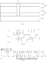
- FIG.2 is waveform diagram of a first clock signal and second clock signal.
- CK1 represents the first clock signal
- CK21 and CK22 represent two types of second clock signals, respectively.
- the second clock cycle is greater than the first clock cycle.
- the first rising edge A1 and the second rising edge A2 are in different level period of the second clock signal, respectively, such that the first rising edge A1 can be distinguished from the second rising edge A2.
- the first falling edge B1 can be distinguished from the second falling edge B2.
- the first rising edge A1 can appear in the period of high level signal of the second clock signal
- the second rising edge A2 appears in the period of low level signal of the second clock signal, or vice versa. The same applies for the first falling edge B1 and the second falling edge B2.
- the first rising edge A1 and the first falling edge B1 appear in the period of high level signal of CK21
- the second rising edge A2 and the second falling edge B2 appear in the period of low level signal of CK21.
- first clock signal and the second signal is not limited to the situation illustrated in FIG. 2 .
- Those skilled in the art can set by themselves as long as different clock edges of the first clock signal can be distinguished based on the second clock signal as mentioned above.
- the second clock cycle is equal to 2 times the first clock cycle. That is, the first clock cycle is equal to a half of the second clock cycle. In this way, it is advantageous to further avoid that the first rising edge and the second rising edge appear at the same level signal period of the second clock cycle and that the first falling edge and the second falling edge appear at the same level signal period of the second clock cycle. It is to be noted that the second clock cycle may also be other times the first clock cycle, which is not limited in the embodiment of the present disclosure.
- the plurality of storage chips include a first storage chip set 110 and a second storage chip set 120.
- the storage chips of the first storage chip set 110 are configured to perform information interaction with the control chip 114 by adopting the first rising edge and/or the first falling edge.
- the storage chips of the second storage chip set 120 are configured to perform information interaction with the control chip 114 by adopting the second rising edge and/or the second falling edge.
- the information interaction includes reading operation and writing operation.
- the first storage chip set 110 performs information interaction with the control chip 114 by adopting the first rising edge and the first falling edge
- the second storage chip set 120 performs information interaction with the control chip 114 by adopting the second rising edge and the second falling edge.
- the first storage chip set 110 includes a first storage chip 111 and a second storage chip 112.
- the second storage chip set 120 includes a third storage chip 121 and a fourth storage chip 122. That is, four storage chips share the channel 01.
- the first storage chip 111 performs information interaction with the control chip 114 at the first rising edge
- the second storage chip 121 performs information interaction with the control chip 114 at the first falling edge
- the second storage chip set 120 includes a third storage chip 121 and a fourth storage chip 122, the third storage chip 121 performs information interaction with the control chip 114 at the second rising edge, and the fourth storage chip 122 performs information interaction with the control chip 114 at the second falling edge.
- first storage chip 111 and the second storage chip 112 may be located in adjacent layers, or may also be spaced by other storage chips.
- the third storage chip 121 and the fourth storage chip 122 may be located in adjacent layers, or may also be spaced by other storage chips.
- an overall macroscopic operation mode of the first storage chip 111 and the second storage chip 112 is: data are transmitted at both the first rising edge and the first falling edge of the first clock signal. Therefore, the data are transmitted at one of the first rising edge or the first falling edge of the first clock signal as for the single storage chip, but the data may be transmitted at both the first rising edge and the first falling edge of the first clock signal as for the overall memory.
- the third storage chip 121 and the fourth storage chip 122 also work at different clock states of the same first clock signal, and also have the effect that the data are transmitted at both the second rising edge and the second falling edge as for the overall memory.
- the first clock signal includes a first command clock and a first data clock.
- the first storage chip 111 performs information interaction with the control chip 114 at a first rising edge of the first command clock and/or the first data clock; and the second storage chip 112 performs information interaction with the control chip 114 at a first falling edge of the first command clock and/or the first data clock.
- the third storage chip 121 performs information interaction with the control chip 114 at a second rising edge of the first command clock and/or the first data clock; and the fourth storage chip 122 performs information interaction with the control chip 114 at a second falling edge of the first command clock and/or the first data clock.
- the first storage chip 111 is configured to receive a command signal at the first rising edge of the first command clock.
- the command signal is configured to control read/write operation of the first storage chip 111, and receive a data signal to be written into the first storage chip 111 or send the data signal at the first rising edge of the corresponding data clock.
- Relevant description related to the second storage chip 112, the third storage chip 121 and the fourth storage chip 122 may refer to the first storage chip 111.
- the first command clock and the first data clock adopt the same first clock signal.
- circuit design is simplified advantageously, a data receiving or sending error caused by an error generated by handshake or synchronization of the first command clock and the first data clock is avoided, and a storage accurate rate of the memory is increased.
- FIG. 3 is a timing diagram of an operation signal corresponding to each storage chip in the memory provided by the embodiment.
- CK1 is the first clock signal
- CK2 is the second clock signal
- DATA1 is a timing diagram of data transmission by the first storage chip 111
- DATA2 is a timing diagram of data transmission by the second storage chip 112
- DATA3 is a timing diagram of data transmission by the third storage chip 121
- DATA4 is a timing diagram of data transmission by the fourth storage chip 122
- DATA is a timing diagram combining DATA1, DATA2, DATA3 and DATA4.
- the first storage chip 111 receives an activation command signal; at the first rising edge of another first clock cycle of the first clock signal, the first storage chip 111 receives a read command signal; and at the first rising edge of another first clock cycle of the first clock signal, the first storage chip 111 transmits data.
- the second storage chip 112 receives an activation command signal; at the first falling edge of the first clock signal, the second storage chip 112 receives a read command signal; and at the first falling edge of the first clock signal, the second storage chip 112 transmits data. In this way, the first storage chip 111 transmits the data at the different first rising edges of the first clock signal, and the second storage chip 112 transmits the data at the different first falling edges of the first clock signal, until data transmission is completed.
- the third storage chip 121 receives an activation command signal; at the second rising edge of the second clock signal, the third storage chip 121 receives a read command signal; and at the second rising edge of the second clock signal, the third storage chip 121 transmits data.
- the fourth storage chip 122 receives an activation command signal; at the second falling edge of the second clock signal, the fourth storage chip 122 receives a read command signal; and at the second falling edge of the second clock signal, the fourth storage chip 122 transmits data.
- the third storage chip 121 transmits the data at the different second rising edges of the second clock signal
- the fourth storage chip 122 transmits the data at the different second falling edges of the second clock signal, until data transmission is completed.
- the first rising edge and the second rising edge can be identified with reference to the second clock signal. Therefore, it can be implemented that the first storage chip 111 operates at the first rising edge and the third storage chip 121 operates at the second rising edge. Similarly, the first falling edge and the second falling edge can also be identified with reference to the second clock signal. Therefore, it can be implemented that the second storage chip 112 operates at the first falling edge and the fourth storage chip 122 operates at the second falling edge.
- the above illustration takes an example that the memory performs read operation.
- the first storage chip 111 and the second storage chip 112 also transmit data alternately
- the third storage chip 121 and the fourth storage chip 122 also transmit data alternately.
- the first storage chip set 110 includes the two storage chips
- the second storage chip set 120 includes the two storage chips. That is, plurality of storage chips are configured to perform information interaction with the control chip 114 by adopting different clock edges of the first clock signal.
- the first clock signal has a first clock cycle. Different clock edges include two consecutive rising edges and two consecutive falling edges. That is, four storage chips share the channel 01.
- plurality of storage chips can also be configured to perform information interaction with the control chip by adopting different clock edges of the first clock signal, and different clock edges include two consecutive rising edges and further include a single falling edge between the two rising edges.
- the first storage chip set includes two storage chips, one storage chip performs information interaction with the control chip at the first rising edge and another storage chip performs information interaction with the control chip at the first falling edge.
- the second storage set may be a single storage chip, and this storage chip may perform information interaction with the control chip at the second rising edge. That is, three storage chips share the channel.
- plurality of storage chips can further be configured to perform information interaction with the control chip by adopting different clock edges of the first clock signal, and different clock edges include two consecutive falling edges and further include a single rising edge between two falling edges.
- the first storage chip set may be a single storage chip, this storage chip performs information interaction with the control chip at the first falling edge.
- the second storage set includes two storage chips, one storage chip performs information interaction with the control chip at the first rising edge and another storage chip performs information interaction with the control chip at the second falling edge. That is, three storage chips share the channel.
- the plurality of storage chips share the communication channel 01, and therefore, under the premise of not influencing a band width of the information interaction of the control chip 114 and the plurality of storage chips, the number of the communication channel 01 of the memory is decreased, and therefore the manufacturing cost and power consumption of the memory are reduced.
- Another embodiment of the present disclosure further provides a memory.
- the memory is roughly the same as the above-mentioned embodiment, and the main difference includes more detailed illustration on each storage chip.
- the memory provided by the embodiment will be illustrated below in detail with reference to the drawings. It is to be noted that, the part the same as or corresponding to the above-mentioned embodiment may refer to the illustration of the above-mentioned embodiment, which will be not repeated hereinafter.
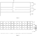
- FIG. 4 is a schematic structural diagram of the memory provided by another embodiment of the present disclosure.
- FIG. 5 is a schematic structural diagram of one storage chip in FIG. 4 .
- the memory includes: a control chip 214; and a plurality of storage chips, in which the plurality of storage chips include a first storage chip set 210 and a second storage chip set 220, and the above-mentioned information interaction includes read/write operation.
- Each storage chip includes at least one channel 20.
- the channel 20 includes: a plurality of storage banks 201, in which each storage bank 201 includes a plurality of storage units, and the plurality of storage banks 201 are configured to perform the read/write operation alternately; a command port 202, in which the command port 202 is configured to receive a command signal at a corresponding clock edge, and the command signal is configured to control the read/write operation of the storage banks 201; and a data port 203, in which the data port 203 is configured to receive a data signal to be written into the storage banks 201 or send the data signal at the corresponding clock edge.
- the command port 202 includes a row address port 212 and a column address port 222, the row address port 212 is configured to receive a row address signal of a position where a target storage unit is located, the column address port 222 is configured to receive a column address signal of the position where the target storage unit is located, and the target storage unit is a storage unit selected from the plurality of storage units.
- the corresponding clock edge refers to a first rising edge or falling edge of the first clock signal.
- command port called in the embodiment includes a port for transmitting the command signal and the address signal, but is not limited to this.
- each storage bank 201 may be distributed in an array.
- each channel 20 includes four storage banks 201
- the four storage banks 201 in one channel 20 are illustrated as bank10, bank11, bank12 and bank13 in FIG. 5 . It may be understood that in other embodiments, the number of the storage banks included in each channel may also be any other number, such as two or six.
- the data port 203 is configured to receive data to be stored into the storage units or send the data read from the storage units.
- the storage chips include the plurality of channels 20, and the storage chips further include a common circuit 204 shared by the plurality of channels 20.
- the common circuit 204 may be a test control circuit, and the test control circuit is configured to control testing of the plurality of channels 20.
- the common circuit may also be at least one of a temperature sensor circuit, an analogy circuit or a charge pump circuit.
- the memory may further include: a test port. Under a test mode, the plurality of channels 20 share the same test port for testing. Since the common test port is disposed, the number of ports in the memory is decreased advantageously, thereby reducing the difficulty of testing the memory through a probe card, and reducing the manufacturing difficulty of the probe card.
- the corresponding clock edge includes the first rising edge and/or the first falling edge; and as for the storage chips in the second storage chip set 220, the corresponding clock edge includes the second rising edge and/or the second falling edge.
- the command signal includes activation commands and read commands corresponding to respective activation commands.
- the channel 20 is further configured such that the command port 202 receives the read command corresponding to the activation command after the command port 202 receives the activation command for a storage bank. More specifically, the activation command includes the row address signal, and the row address signal is received through the row address port 212; and the read command includes the column address signal, and the column address signal is received through the column address port 222. It is to be noted that the activation command and the read command may further contain other control signals except the row address signal or the column address signal.
- control signals are configured to help or assist the storage chips to recognize whether the command is the activation command or the read command, and these other control signals may be received through other command ports except the row address port 212 and the column address port 222.
- the row address port 212 may continuously receive the row address signal
- the column address port 222 may continuously receive the column address signal.
- the channel 20 is further configured such that the activation command and the read command are received through different ports in the command port 202, and thus the activation command and the read command may be received simultaneously.
- the channel 20 is further configured such that the data port 203 sends the data signal after the command port 202 receives the read command.
- the command signal includes the activation command and the read command corresponding to the activation command.
- the channel is further configured such that after the command port 202 alternately receives the activation commands for the different storage banks 201, the command port 202 alternately receives the read commands corresponding to the activation commands. Specifically, after the row address port 212 alternately receives the activation commands for the different storage banks 201, the column address port 222 alternately receives the read commands corresponding to the activation commands.
- the channel is further configured such that the data port 203 alternately sends the data signals corresponding to the different storage banks 201 after the command port 202 receives the read command.
- the first storage chip set 210 includes a first storage chip 211 and a second storage chip 212; and the second storage chip set 220 includes a third storage chip 221 and a fourth storage chip 222.
- first storage chip set 210 For detailed description related to difference between the first storage chip set 210 and the second storage chip set 220, reference may be made to the above-mentioned embodiments. Taking the storage chips in the first storage chip set 210 as an example, and the storage chip 211 operates at the first rising edge, the second storage chip 212 operates at the first falling edge, the third storage chip 221 operates at the second rising edge, and the fourth storage chip 221 operates at the second falling edge, an operation mode of the command port 202 is illustrated below in detail.
- the command port 202 of the first storage chip 211 adopts the first rising edge of the first clock signal to receive or send a signal
- the data port 203 adopts the first rising edge of the first clock signal to receive or send the signal
- the storage chip is denoted as the storage chip C1.
- the command port 202 of the second storage chip 212 adopts the first falling edge of the first clock signal to receive or send a signal
- the data port 203 adopts the first falling edge of the first clock signal to receive or send the signal
- the storage chip is denoted as the storage chip C2.
- the command port 202 of the third storage chip 221 adopts the second rising edge of the first clock signal to receive or send a signal
- the data port 203 adopts the second rising edge of the first clock signal to receive or send the signal
- the storage chip is denoted as the storage chip C3.
- the command port 202 of the fourth storage chip 222 adopts the second falling edge of the first clock signal to receive or send a signal
- the data port 203 adopts the second falling edge of the first clock signal to receive or send the signal
- the storage chip is denoted as the storage chip C4.
- FIG. 6 is a timing diagram of the operations of the storage chips C1/C2/C3/C4. The operating principle of the memory will be illustrated below with reference to the timing diagram.
- CK1 shows the first clock signal
- CK2 shows the second clock signal
- ACT1/ACT2/ACT3/ACT4 correspondingly show the timing diagram of the activation command signals for the storage chips C1/C2/C3/C
- RD1/RD2/RD3/RD4 show the timing diagram of the read command signals for the storage chips C1/C2/C3/C4
- DATA1/DATA2/DATA3/DATA4 show the timing diagram of the data signals of the data ports of the storage chips C1/C2/C3/C4.
- the activation command signal ACT1 includes A10/A11/A12/A13 configured to activate bank10, bank11, bank12 and bank13 respectively, A10 corresponds to bank10, A11 corresponds to bank11, and so on.
- the read command signal RD1 includes R10/R11/R12/R13 corresponding to bank10, bank11, bank12 and bank13 one to one, and the data signal DATA1 includes D10/D11/D12/D13.
- the detailed illustration related to the activation command signals A20/A21/A22/A23, the read command signals R20/R21/R22/R23 and the data signals D20/D21/D22/D23 corresponding to the storage chip C2, the activation command signals A30/A31/A32/A33, the read command signals R30/R31/R32/R33 and the data signals D30/D31/D32/D33 corresponding to the storage chip C3, and the activation command signals A40/A41/A42/A43, the read command signals R40/R41/R42/R43 and the data signals D40/D41/D42/D43 corresponding to the storage chip C4 may refer to the above-mentioned illustration.
- the command port 202 and the data port 203 adopt the first rising edge of the first clock to receive or send a signal: after the command port 202 receives the activation command A10 for one storage bank 201 (refer to FIG. 5 ) at the first rising edge of the first clock signal, the command port 202 receives one read command R10 corresponding to the activation command A10 at the rising edge; and after the command port 202 receives the read command R10, the data port 203 sends the data signal D10 at the first rising edge of the first clock signal.
- the flow after the command port 202 receives the activation commands A11/A12/A13 is similar to that of the above mentioned.
- the row address port 212 in the command port 202 receives the activation command A10 for activating bank10 at the first rising edge of the first clock signal
- the row address port 212 in the command port 202 receives the activation command A11 for activating bank11 at the first rising edge of the first clock signal
- the column address port 222 in the command port 202 receives the read command R10 corresponding to the activation command A10 at the first rising edge, and the command port 202 receives the read command R11 corresponding to the activation command A11 at the first rising edge, receives the read command R12 corresponding to the activation command A12 at the first rising edge, and receives the read command R13 corresponding to the activation command A13 at the first rising edge, in which n is any natural number.
- the data port 203 sends the data signal D10 corresponding to the storage bank bank10 at the first rising edge of the first clock signal, and the data port 203 sends the data signal D11 corresponding to the storage bank bank11 at the first rising edge of the first clock signal, sends the data signal D12 corresponding to bank12 at the first rising edge, and sends the data signal D13 corresponding to bank13 at the first rising edge, in which m is any natural number.
- FIG.6 takes an example that the activation commands A10, A11, A12 and A13 are received respectively at the continuous first rising edge, that is, the activation commands corresponding to the different storage banks 201 are received respectively at the continuous first rising edge.
- the activation commands corresponding to the different storage banks may also be received respectively at non-continuous first rising edges.
- the row address port 212 and the column address port 222 are not shared, and therefore, during the period that the column address port 222 receives the read command R10, the row address port 212 may receive the activation command A12.
- the activation commands can be received without the need of waiting all the read command signals to be completely received, thus a data bus may be filled, that is, the data port 203 may transmit the data continuously, thereby avoiding the idle problem of the data bus in a certain period of time, and increasing the storage speed of the memory advantageously.
- the command port 202 and the data port 203 adopt the falling edge of the first clock signal to receive or send a signal: after the command port 202 receives the activation command A0 for one storage bank 201 at the first falling edge of the first clock signal, the command port 202 receives one read command R20 corresponding to the activation command A20 at the first falling edge; and after the command port 202 receives the read command R20, the data port 203 sends the data signal D20 at the first falling edge of the first clock signal.
- a process related to the storage chip C2 sending the data signals D21/D22/D23 will not be repeated in detail.
- the storage chips C1/C2/C3/C4 receive or send the signals at the first rising edge, the first falling edge, the second rising edge and the second falling edge of the first clock cycle of the first clock signal, so that the four storage chips sharing the communication channel 02 transmit the data without interfering each other.
- the command signal includes activation commands and a plurality of read commands corresponding to each activation command.
- the channel 20 is further configured such that after the command port 202 receives the activation command for a storage bank 201, the command port 202 receives one read command corresponding to the activation command at the plurality of corresponding clock edges, that is, the command port 202 receives the plurality of read commands corresponding to the activation commands at the plurality of consecutive corresponding clock edges.
- the channel 20 is further configured such that the data port 203 sends the plurality of data signals at the plurality of consecutive corresponding clock edges, and the number of the data signals is the same as the number of the received read commands.
- the activation command includes the row address signal
- the read command includes the column address signal.
- the channel 20 is further configured such that the activation command and the read command are received through the different ports in the command port.
- the command signal may include the activation commands and a plurality of read commands corresponding to each activation command.
- the channel 20 may further be configured such that the command port 202 alternately receives the plurality of read commands corresponding to each activation command after the command port 202 alternately receives the activation commands for the different storage banks 201.
- the command port 202 receives one read command corresponding to the activation command at each clock edge in the plurality of corresponding clock edges, so that the command port 202 receives the plurality of read commands corresponding to the activation commands at the plurality of continuous clock edges, until the command port 202 receives the plurality of read commands corresponding to the activation command, and then the command port 202 receives the plurality of read commands corresponding to the activation command for another storage bank 201.
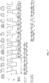
- FIG. 7 is another timing diagram of operations of the first storage chip set 210 and the second storage chip set 220.
- the operating principle of the memory will be illustrated below with reference to FIG. 7 , taking an example that one activation command corresponds to four read commands.
- Illustration related to all the signals in FIG. 7 may refer to corresponding illustration in FIG. 6 , and main difference corresponding to FIG. 6 includes: the activation command A10 configured to activate bank10 corresponds to the four read commands R10 and the four data signals D10, the activation command A11 configured to activate bank11 corresponds to the four read commands R11 and the data signals D11, and so on. That is, one activation command corresponds to the plurality of different read commands.
- the command port 202 receives the activation command A10 for one storage bank 201 at the first rising edge of the first clock signal
- the command port 202 receives the four read commands R10 corresponding to the activation command A10 at the four continuous first rising edges
- the data port 203 sends the four data signals D10 at the first rising edge of the first clock signal.
- the command port 202 After receiving the activation command A11 for another storage bank 201, the command port 202 receives the four read commands R11 corresponding to the activation command A11 at the four continuous first rising edges, and after the command port 202 receives the read commands R11, the data port 203 sends the four data signals D11 at the first rising edge of the first clock signal.
- the flow after the command port 202 receives the activation commands A12 and A13 is similar to that of the above mentioned.
- the storage chip C2 sends or receives the signal at the first falling edge of the first clock signal, that is, the storage chip C2 performs information interaction with the control chip 214 at the first falling edge of the first clock signal.
- the storage chip C3 performs information interaction with the control chip 214 at the second rising edge of the first clock signal, and the storage chip C4 performs information interaction with the control chip 214 at the second falling edge of the first clock signal.
- the operating principle of the storage chips C2/C3/C4 may refer to the operating principle of the storage chip C1.
- the channel 20 is further configured: as for any storage bank 201, a time reference between receiving the activation command and receiving the corresponding read command is larger than or equal to tRCD, and tRCD is the shortest preparation time for performing the read operation by the storage bank 201 after receiving the activation command.
- tRCD is the shortest preparation time for performing the read operation by the storage bank 201 after receiving the activation command.
- the definition about tRCD is: an interval from line validness to sending of the read/write command is defined as tRCD, namely, delay from RAS to CAS, RAS is a row address strobing pulse signal, or the row address signal for short, CAS is a column address strobing pulse signal, or the column address signal for short, and tRCD may be understood as a row strobing period.
- the time difference between A10 and R10 is tRCD; and as for bank11, the time difference between A11 and R11 may be larger than or equal to tRCD.
- the situations with respect to bank12 and bank13 are not listed one by one here. Whether one activation command corresponds to one read command or the plurality of read commands, it may be ensured through reasonable setting that the time reference between receiving the command signal and receiving the corresponding read command signal is larger than or equal to tRCD as for any storage bank 201.
- the different storage banks 201 adopt the same command port 202 and the same data port 203. In other embodiments, the different storage banks may also adopt different command ports and different data ports.
- the memory provided by the embodiment may realize simultaneous transmission of the row address signal and the column address signal due to the fact that the row address port 212 and the column address port 222 are separated, a data receiving or sending error caused by an error generated by handshake or synchronization of the command clock and the data clock is avoided, thus the problem that the data cable is not occupied completely at the certain time periods is avoided advantageously, and it is ensured that the data cable is occupied completely by the data all the time, thereby increasing the storage speed of the memory, and improving the storage performance of the memory.
Landscapes
- Engineering & Computer Science (AREA)
- Theoretical Computer Science (AREA)
- Computer Hardware Design (AREA)
- Physics & Mathematics (AREA)
- General Engineering & Computer Science (AREA)
- General Physics & Mathematics (AREA)
- Microelectronics & Electronic Packaging (AREA)
- Software Systems (AREA)
- Databases & Information Systems (AREA)
- Mathematical Physics (AREA)
- Dram (AREA)
- Static Random-Access Memory (AREA)
Abstract
Description
- This application is based on the disclosure of
Chinese patent application No. 202010873269.6 filed on August 26, 2020 - Embodiments of the present disclosure relate to, but are not limited to, the technical field of semiconductors, and in particular to a memory.
- A Dynamic Random Access Memory (DRAM) is a common semiconductor storage device in a computer and is composed of many repeated storage units. Each storage unit usually includes a capacitor and a transistor. Gates of the transistors are connected with a word line, drains of the transistors are connected with a bit line, and sources of the transistors are connected with the capacitors. Voltage signals on the word line can control on or off of the transistors, so that data information stored in the capacitors is read through the bit line, or the data information is written into the capacitors for storage through the bit line.
- With more and more application fields of the DRAM, for example, the DRAM is increasingly applied to various fields, a user has higher and higher requirements for a performance index of the DRAM, and has different requirements for the DRAM due to the different application fields.
- An embodiment of the present disclosure provides a memory, including: a control chip; and a plurality of storage chips, in which the plurality of storage chips are electrically connected with the control chip via a common communication channel, the plurality of storage chips are configured to perform information interaction with the control chip by adopting different clock edges of a first clock signal, the first clock signal has a first clock cycle, the different clock edges include two consecutive rising edges and/or two consecutive falling edges, the plurality of storage chips are further configured to receive a second clock signal and distinguish the different clock edges based on the second clock signal, and a second clock cycle of the second clock signal is greater than the first clock cycle.
- In some embodiments, the different clock edges include a first rising edge, a first falling edge, a second rising edge and a second falling edge that are consecutive; the plurality of storage chips include a first storage chip set and a second storage chip set; storage chips of the first storage chip set are configured to perform information interaction with the control chip by adopting the first rising edge and/or the first falling edge; and storage chips of the second storage chip set are configured to perform information interaction with the control chip by adopting the second rising edge and/or the second falling edge.
- In some embodiments, the first clock cycle is equal to 1/2 times the second clock cycle.
- In some embodiments, each storage chip includes at least one channel. The channel includes: a plurality of storage banks, in which each storage bank includes a plurality of storage units, and the plurality of storage banks are configured to perform read/write operation alternately; a command port, in which the command port is configured to receive a command signal at a corresponding clock edge, and the command signal is configured to control the read/write operation of the storage banks; and a data port, in which the data port is configured to receive a data signal to be written into the storage banks or send the data signal at the corresponding clock edge. The command port includes a row address port and a column address port, the row address port is configured to receive a row address signal of a position where a target storage unit is located, the column address port is configured to receive a column address signal of the position where the target storage unit is located, and the target storage unit is a storage unit selected from the plurality of storage units.
- In some embodiments, the command signal includes activation commands and read commands corresponding to respective activation commands. The channel is further configured such that the command port receives the read command corresponding to the activation command after the command port receives the activation command for a storage bank.
- In some embodiments, the channel is further configured such that the data port sends the data signal after the command port receives the read command.
- In some embodiments, the command signal includes activation commands and a plurality of read commands corresponding to each activation command. The channel is further configured such that after the command port receives the activation command for a storage bank, the command port receives one read command corresponding to the activation command at the plurality of corresponding clock edges, to receive the plurality of read commands corresponding to the activation command at the plurality of consecutive corresponding clock edges.
- In some embodiments, the channel is further configured such that the data port sends a plurality of data signals at the plurality of consecutive corresponding clock edges respectively, and the number of the data signals is the same as the number of the received read commands.
- In some embodiments, the command signal includes an activation command and a read command corresponding to the activation command. The channel is further configured such that the command port alternately receives the read commands corresponding to the activation commands after the command port alternately receives the activation commands for the different storage banks.
- In some embodiments, the channel is further configured such that the data port alternately sends the data signals corresponding to the different storage banks after the command port receives the read command.
- In some embodiments, the command signal includes activation commands and a plurality of read commands corresponding to each activation command. The channel is further configured such that the command port alternately receives the activation commands for the different storage banks, and the command port alternately receives the plurality of read commands corresponding to each activation command.
- In some embodiments, the activation command includes the row address signal, and the read command includes the column address signal. The channel is further configured such that the activation command and the read command are received through different ports in the command port.
- In some embodiments, the storage chips include a plurality of channels, and the storage chips further include a common circuit shared by the plurality of channels.
- In some embodiments, the storage chips further include: a test port. Under a test mode, the plurality of channels share the same test port for testing.
- In some embodiments, the common circuit includes a test control circuit, and the test control circuit is configured to control testing of the plurality of channels.
- In some embodiments, the plurality of storage chips are sequentially stacked on the control chip, and the communication channel includes a through silicon via.
- The technical solution provided by the embodiment of the present disclosure has at least the following advantages:
- The embodiment of the present disclosure provides the memory with excellent structural performance. The plurality of storage chips share the communication channel to be electrically connected with the control chip. The plurality of storage chips are configured to perform information interaction with the control chip by adopting different clock edges of a first clock signal, the first clock signal has a first clock cycle, the different clock edges include two consecutive rising edges and/or two consecutive falling edges, the plurality of storage chips are further configured to receive a second clock signal and distinguish the different clock edges based on the second clock signal, and a second clock cycle of the second clock signal is greater than the first clock cycle. The plurality of storage chips share the communication channel to be electrically connected with the control chip, therefore, there is no need to dispose a communication channel electrically connected with the control chip for each storage chip, thereby decreasing the number of the communication channels required by the memory advantageously, and reducing the cost and the power consumption of the memory accordingly.
- In some embodiments, the row address port and the column address port are separated, therefore the row address signal and the column address signal may be transmitted simultaneously, avoiding the problem that an activation command signal can only be transmitted after the read command is transmitted. Thus, the problem that a data cable is not occupied completely at certain time periods is avoided advantageously, and it is ensured that the data cable is occupied completely by data all the time, thereby increasing the storage speed of the memory, and improving the storage performance of the memory.
- One or more embodiments are exemplarily illustrated through diagrams in the drawings corresponding thereto, and unless otherwise specifically specified, the graphs in the drawings do not limit the proportion.
-
FIG. 1 is a schematic structural diagram of a memory provided by an embodiment of the present disclosure. -
FIG. 2 is two different oscillograms of a first clock signal and second clock signal. -
FIG. 3 is a timing diagram of an operation signal corresponding to each storage chip in a memory provided by an embodiment of the present disclosure. -
FIG. 4 is a schematic structural diagram of a memory provided by another embodiment of the present disclosure. -
FIG. 5 is a schematic structural diagram of a storage chip inFIG. 4 . -
FIG. 6 is a timing diagram of operations of all storage chips in a memory provided by another embodiment of the present disclosure. -
FIG. 7 is another timing diagram of operations of all storage chips in a memory provided by another embodiment of the present disclosure. - It can be known from the background that performance of a memory needs to be improved currently.
- An embodiment of the present disclosure provides a memory, including a plurality of storage chips. The plurality of storage chips share a communication channel to be electrically connected with a control chip. The plurality of storage chips are configured to perform information interaction with the control chip by adopting different clock edges of a first clock signal, the first clock signal has a first clock cycle, and the different clock edges comprises two consecutive rising edges and/or two consecutive falling edges. The plurality of storage chips are further configured to receive a second clock signal and distinguish the different clock edges based on the second clock signal, and a second clock cycle of the second clock signal is greater than the first clock cycle. Since the plurality of storage chips share the communication channel, under the premise of not influencing the quality of information interaction between the plurality of storage chips and the control chip, the number of the communication channel required by the memory is decreased, thereby saving the area of the memory, reducing the cost of the memory, and reducing power consumption of the memory.
- In order to make the objective, technical solutions and advantages of the embodiments of the present disclosure more clear, all the embodiments of the present disclosure will be described below in detail with reference to the drawings. However, the ordinary skilled in the art may understand that a lot of technical details are proposed to make the present disclosure better understood by a reader in the embodiments of the present disclosure. However, the technical solution claimed in the present disclosure can also be implemented without these technical details and various changes and modifications based on the following embodiments.
-
FIG. 1 is a schematic structural diagram of a memory provided by an embodiment of the present disclosure. - Referring to
FIG. 1 , in the embodiment, the memory includes: acontrol chip 114; and a plurality of storage chips, in which the plurality of storage chips share acommunication channel 01 to be electrically connected with thecontrol chip 114. The plurality of storage chips are configured to perform information interaction with thecontrol chip 114 by adopting different clock edges of a first clock signal, the first clock signal has a first clock cycle, and the different clock edges comprises two consecutive rising edges and/or two consecutive falling edges. The plurality of storage chips are further configured to receive a second clock signal and distinguish the different clock edges based on the second clock signal, and a second clock cycle of the second clock signal is greater than the first clock cycle. - The memory provided by the embodiment will be illustrated below in detail with reference to the drawings.
- In the embodiment, the memory may be a dynamic random access memory.
- Specifically, the plurality of storage chips may be sequentially stacked on the
control chip 114, thereby improving a storage density and decreasing a distance between the storage chips and thecontrol chip 114 advantageously. Or, the plurality of storage chips may also be disposed on thecontrol chip 114 side by side, thereby reducing a longitudinal thickness of the memory advantageously. In the embodiment, the plurality of storage chips are sequentially stacked on thecontrol chip 114, and thecommunication channel 01 includes a Through Silicon Via (TSV). - Specifically, different clock edges include a first rising edge, a first falling edge, a second rising edge and a second falling edge that are consecutive. It could be considered that the first rising edge and the first falling edge are the clock edges within the previous first clock cycle. The second rising edge and the second falling edge are the clock edges within the next first clock cycle. The second clock signal is used as the reference for distinguishing different clock edges, such that different clock edges of the same first clock cycle (first rising edge/first falling edge/second rising edge/second falling edge) can be distinguished from each other. In this way, although plurality of storage chips share the
communication channel 01, each storage chip can perform information interaction with thecontrol chip 114 by adopting the corresponding clock edge. - Specifically, as illustrated in
FIG. 2, FIG.2 is waveform diagram of a first clock signal and second clock signal. CK1 represents the first clock signal, and CK21 and CK22 represent two types of second clock signals, respectively. The second clock cycle is greater than the first clock cycle. In this way, the first rising edge A1 and the second rising edge A2 are in different level period of the second clock signal, respectively, such that the first rising edge A1 can be distinguished from the second rising edge A2. Similarly, the first falling edge B1 can be distinguished from the second falling edge B2. In an embodiment, the first rising edge A1 can appear in the period of high level signal of the second clock signal, and the second rising edge A2 appears in the period of low level signal of the second clock signal, or vice versa. The same applies for the first falling edge B1 and the second falling edge B2. - As illustrated in CK1 and CK21 in
FIG. 2 , the first rising edge A1 and the first falling edge B1 appear in the period of high level signal of CK21, and the second rising edge A2 and the second falling edge B2 appear in the period of low level signal of CK21. - It is to be noted that the position relationship of the first clock signal and the second signal is not limited to the situation illustrated in
FIG. 2 . Those skilled in the art can set by themselves as long as different clock edges of the first clock signal can be distinguished based on the second clock signal as mentioned above. - In the embodiment, the second clock cycle is equal to 2 times the first clock cycle. That is, the first clock cycle is equal to a half of the second clock cycle. In this way, it is advantageous to further avoid that the first rising edge and the second rising edge appear at the same level signal period of the second clock cycle and that the first falling edge and the second falling edge appear at the same level signal period of the second clock cycle. It is to be noted that the second clock cycle may also be other times the first clock cycle, which is not limited in the embodiment of the present disclosure.
- The plurality of storage chips include a first storage chip set 110 and a second
storage chip set 120. The storage chips of the first storage chip set 110 are configured to perform information interaction with thecontrol chip 114 by adopting the first rising edge and/or the first falling edge. The storage chips of the second storage chip set 120 are configured to perform information interaction with thecontrol chip 114 by adopting the second rising edge and/or the second falling edge. The information interaction includes reading operation and writing operation. - Detailed description will be made in an example in which the first storage chip set 110 performs information interaction with the
control chip 114 by adopting the first rising edge and the first falling edge, and the second storage chip set 120 performs information interaction with thecontrol chip 114 by adopting the second rising edge and the second falling edge. The first storage chip set 110 includes a first storage chip 111 and asecond storage chip 112. The second storage chip set 120 includes athird storage chip 121 and afourth storage chip 122. That is, four storage chips share thechannel 01. - In the embodiment, as illustrated in
FIG. 1 , the first storage chip 111 performs information interaction with thecontrol chip 114 at the first rising edge, and thesecond storage chip 121 performs information interaction with thecontrol chip 114 at the first falling edge. The second storage chip set 120 includes athird storage chip 121 and afourth storage chip 122, thethird storage chip 121 performs information interaction with thecontrol chip 114 at the second rising edge, and thefourth storage chip 122 performs information interaction with thecontrol chip 114 at the second falling edge. - It is to be noted that the first storage chip 111 and the
second storage chip 112 may be located in adjacent layers, or may also be spaced by other storage chips. Thethird storage chip 121 and thefourth storage chip 122 may be located in adjacent layers, or may also be spaced by other storage chips. - Since the first storage chip 111 and the
second storage chip 112 work at different clock states of the same first clock signal, an overall macroscopic operation mode of the first storage chip 111 and thesecond storage chip 112 is: data are transmitted at both the first rising edge and the first falling edge of the first clock signal. Therefore, the data are transmitted at one of the first rising edge or the first falling edge of the first clock signal as for the single storage chip, but the data may be transmitted at both the first rising edge and the first falling edge of the first clock signal as for the overall memory. Similarly, thethird storage chip 121 and thefourth storage chip 122 also work at different clock states of the same first clock signal, and also have the effect that the data are transmitted at both the second rising edge and the second falling edge as for the overall memory. - Furthermore, the first clock signal includes a first command clock and a first data clock. As for the first storage chip set 110, the first storage chip 111 performs information interaction with the
control chip 114 at a first rising edge of the first command clock and/or the first data clock; and thesecond storage chip 112 performs information interaction with thecontrol chip 114 at a first falling edge of the first command clock and/or the first data clock. As for the second storage chip set 120, thethird storage chip 121 performs information interaction with thecontrol chip 114 at a second rising edge of the first command clock and/or the first data clock; and thefourth storage chip 122 performs information interaction with thecontrol chip 114 at a second falling edge of the first command clock and/or the first data clock. - Taking the first storage chip 111 as an example, the first storage chip 111 is configured to receive a command signal at the first rising edge of the first command clock. The command signal is configured to control read/write operation of the first storage chip 111, and receive a data signal to be written into the first storage chip 111 or send the data signal at the first rising edge of the corresponding data clock. Relevant description related to the
second storage chip 112, thethird storage chip 121 and thefourth storage chip 122 may refer to the first storage chip 111. - In the embodiment, in order to reduce complexity of the memory, the first command clock and the first data clock adopt the same first clock signal. In this way, circuit design is simplified advantageously, a data receiving or sending error caused by an error generated by handshake or synchronization of the first command clock and the first data clock is avoided, and a storage accurate rate of the memory is increased.
- It is to be noted that in other embodiments, the first command clock and the first data clock may also adopt different first clock signals.
FIG. 3 is a timing diagram of an operation signal corresponding to each storage chip in the memory provided by the embodiment. CK1 is the first clock signal, CK2 is the second clock signal, DATA1 is a timing diagram of data transmission by the first storage chip 111, DATA2 is a timing diagram of data transmission by thesecond storage chip 112, DATA3 is a timing diagram of data transmission by thethird storage chip 121, DATA4 is a timing diagram of data transmission by thefourth storage chip 122, and DATA is a timing diagram combining DATA1, DATA2, DATA3 and DATA4. - An operating principle of the memory provided by the embodiment will be illustrated below with reference to
FIG. 3 . - At the first rising edge for one first clock cycle of the first clock signal, the first storage chip 111 receives an activation command signal; at the first rising edge of another first clock cycle of the first clock signal, the first storage chip 111 receives a read command signal; and at the first rising edge of another first clock cycle of the first clock signal, the first storage chip 111 transmits data. At the first falling edge of the first clock signal, the
second storage chip 112 receives an activation command signal; at the first falling edge of the first clock signal, thesecond storage chip 112 receives a read command signal; and at the first falling edge of the first clock signal, thesecond storage chip 112 transmits data. In this way, the first storage chip 111 transmits the data at the different first rising edges of the first clock signal, and thesecond storage chip 112 transmits the data at the different first falling edges of the first clock signal, until data transmission is completed. - At the second rising edge of the second clock signal, the
third storage chip 121 receives an activation command signal; at the second rising edge of the second clock signal, thethird storage chip 121 receives a read command signal; and at the second rising edge of the second clock signal, thethird storage chip 121 transmits data. At the second falling edge of the second clock signal, thefourth storage chip 122 receives an activation command signal; at the second falling edge of the second clock signal, thefourth storage chip 122 receives a read command signal; and at the second falling edge of the second clock signal, thefourth storage chip 122 transmits data. In this way, thethird storage chip 121 transmits the data at the different second rising edges of the second clock signal, and thefourth storage chip 122 transmits the data at the different second falling edges of the second clock signal, until data transmission is completed. - Since the first rising edge appears at the high level period of the second clock signal and the second rising edge appears at the low level period of the second clock signal, the first rising edge and the second rising edge can be identified with reference to the second clock signal. Therefore, it can be implemented that the first storage chip 111 operates at the first rising edge and the
third storage chip 121 operates at the second rising edge. Similarly, the first falling edge and the second falling edge can also be identified with reference to the second clock signal. Therefore, it can be implemented that thesecond storage chip 112 operates at the first falling edge and thefourth storage chip 122 operates at the second falling edge. - It can be understood that the above illustration takes an example that the memory performs read operation. During a write operation period of the memory, the first storage chip 111 and the
second storage chip 112 also transmit data alternately, and thethird storage chip 121 and thefourth storage chip 122 also transmit data alternately. - In the embodiment, the first storage chip set 110 includes the two storage chips, and the second storage chip set 120 includes the two storage chips. That is, plurality of storage chips are configured to perform information interaction with the
control chip 114 by adopting different clock edges of the first clock signal. The first clock signal has a first clock cycle. Different clock edges include two consecutive rising edges and two consecutive falling edges. That is, four storage chips share thechannel 01. - It is to be noted that, in another example, plurality of storage chips can also be configured to perform information interaction with the control chip by adopting different clock edges of the first clock signal, and different clock edges include two consecutive rising edges and further include a single falling edge between the two rising edges. Correspondingly, taking as an example that a single falling edge is the first falling edge, the first storage chip set includes two storage chips, one storage chip performs information interaction with the control chip at the first rising edge and another storage chip performs information interaction with the control chip at the first falling edge. The second storage set may be a single storage chip, and this storage chip may perform information interaction with the control chip at the second rising edge. That is, three storage chips share the channel.
- Further, in another example, plurality of storage chips can further be configured to perform information interaction with the control chip by adopting different clock edges of the first clock signal, and different clock edges include two consecutive falling edges and further include a single rising edge between two falling edges. Correspondingly, taking as an example that a single rising edge is the second rising edge, the first storage chip set may be a single storage chip, this storage chip performs information interaction with the control chip at the first falling edge. The second storage set includes two storage chips, one storage chip performs information interaction with the control chip at the first rising edge and another storage chip performs information interaction with the control chip at the second falling edge. That is, three storage chips share the channel. According to the memory provided by the embodiment, the plurality of storage chips share the
communication channel 01, and therefore, under the premise of not influencing a band width of the information interaction of thecontrol chip 114 and the plurality of storage chips, the number of thecommunication channel 01 of the memory is decreased, and therefore the manufacturing cost and power consumption of the memory are reduced. - Another embodiment of the present disclosure further provides a memory. The memory is roughly the same as the above-mentioned embodiment, and the main difference includes more detailed illustration on each storage chip. The memory provided by the embodiment will be illustrated below in detail with reference to the drawings. It is to be noted that, the part the same as or corresponding to the above-mentioned embodiment may refer to the illustration of the above-mentioned embodiment, which will be not repeated hereinafter.
-
FIG. 4 is a schematic structural diagram of the memory provided by another embodiment of the present disclosure.FIG. 5 is a schematic structural diagram of one storage chip inFIG. 4 . - Referring to
FIG. 4 and FIG. 5 , in the embodiment, the memory includes: acontrol chip 214; and a plurality of storage chips, in which the plurality of storage chips include a first storage chip set 210 and a second storage chip set 220, and the above-mentioned information interaction includes read/write operation. Each storage chip includes at least one channel 20. The channel 20 includes: a plurality ofstorage banks 201, in which eachstorage bank 201 includes a plurality of storage units, and the plurality ofstorage banks 201 are configured to perform the read/write operation alternately; acommand port 202, in which thecommand port 202 is configured to receive a command signal at a corresponding clock edge, and the command signal is configured to control the read/write operation of thestorage banks 201; and adata port 203, in which thedata port 203 is configured to receive a data signal to be written into thestorage banks 201 or send the data signal at the corresponding clock edge. Thecommand port 202 includes arow address port 212 and acolumn address port 222, therow address port 212 is configured to receive a row address signal of a position where a target storage unit is located, thecolumn address port 222 is configured to receive a column address signal of the position where the target storage unit is located, and the target storage unit is a storage unit selected from the plurality of storage units. - It can be understood that the corresponding clock edge refers to a first rising edge or falling edge of the first clock signal.
- It is to be noted that the command port called in the embodiment includes a port for transmitting the command signal and the address signal, but is not limited to this.
- The memory provided by the embodiment will be illustrated below in detail with reference to the drawings.
- The plurality of storage units in each
storage bank 201 may be distributed in an array. In the embodiment, taking an example that each channel 20 includes fourstorage banks 201, the fourstorage banks 201 in one channel 20 are illustrated as bank10, bank11, bank12 and bank13 inFIG. 5 . It may be understood that in other embodiments, the number of the storage banks included in each channel may also be any other number, such as two or six. - The
data port 203 is configured to receive data to be stored into the storage units or send the data read from the storage units. - The storage chips include the plurality of channels 20, and the storage chips further include a
common circuit 204 shared by the plurality of channels 20. In the embodiment, thecommon circuit 204 may be a test control circuit, and the test control circuit is configured to control testing of the plurality of channels 20. In other embodiments, the common circuit may also be at least one of a temperature sensor circuit, an analogy circuit or a charge pump circuit. - The memory may further include: a test port. Under a test mode, the plurality of channels 20 share the same test port for testing. Since the common test port is disposed, the number of ports in the memory is decreased advantageously, thereby reducing the difficulty of testing the memory through a probe card, and reducing the manufacturing difficulty of the probe card.
- As for the storage chips in the first storage chip set 210, the corresponding clock edge includes the first rising edge and/or the first falling edge; and as for the storage chips in the second storage chip set 220, the corresponding clock edge includes the second rising edge and/or the second falling edge.
- The command signal includes activation commands and read commands corresponding to respective activation commands. The channel 20 is further configured such that the
command port 202 receives the read command corresponding to the activation command after thecommand port 202 receives the activation command for a storage bank. More specifically, the activation command includes the row address signal, and the row address signal is received through therow address port 212; and the read command includes the column address signal, and the column address signal is received through thecolumn address port 222. It is to be noted that the activation command and the read command may further contain other control signals except the row address signal or the column address signal. These other control signals are configured to help or assist the storage chips to recognize whether the command is the activation command or the read command, and these other control signals may be received through other command ports except therow address port 212 and thecolumn address port 222. In this way, therow address port 212 may continuously receive the row address signal, and thecolumn address port 222 may continuously receive the column address signal. Accordingly, the channel 20 is further configured such that the activation command and the read command are received through different ports in thecommand port 202, and thus the activation command and the read command may be received simultaneously. Furthermore, the channel 20 is further configured such that thedata port 203 sends the data signal after thecommand port 202 receives the read command. - In the embodiment, the command signal includes the activation command and the read command corresponding to the activation command. The channel is further configured such that after the
command port 202 alternately receives the activation commands for thedifferent storage banks 201, thecommand port 202 alternately receives the read commands corresponding to the activation commands. Specifically, after therow address port 212 alternately receives the activation commands for thedifferent storage banks 201, thecolumn address port 222 alternately receives the read commands corresponding to the activation commands. - Furthermore, the channel is further configured such that the
data port 203 alternately sends the data signals corresponding to thedifferent storage banks 201 after thecommand port 202 receives the read command. - The first storage chip set 210 includes a
first storage chip 211 and asecond storage chip 212; and the second storage chip set 220 includes athird storage chip 221 and afourth storage chip 222. - For detailed description related to difference between the first storage chip set 210 and the second storage chip set 220, reference may be made to the above-mentioned embodiments. Taking the storage chips in the first storage chip set 210 as an example, and the
storage chip 211 operates at the first rising edge, thesecond storage chip 212 operates at the first falling edge, thethird storage chip 221 operates at the second rising edge, and thefourth storage chip 221 operates at the second falling edge, an operation mode of thecommand port 202 is illustrated below in detail. - The
command port 202 of thefirst storage chip 211 adopts the first rising edge of the first clock signal to receive or send a signal, thedata port 203 adopts the first rising edge of the first clock signal to receive or send the signal, and the storage chip is denoted as the storage chip C1. Thecommand port 202 of thesecond storage chip 212 adopts the first falling edge of the first clock signal to receive or send a signal, thedata port 203 adopts the first falling edge of the first clock signal to receive or send the signal, and the storage chip is denoted as the storage chip C2. Thecommand port 202 of thethird storage chip 221 adopts the second rising edge of the first clock signal to receive or send a signal, thedata port 203 adopts the second rising edge of the first clock signal to receive or send the signal, and the storage chip is denoted as the storage chip C3. Thecommand port 202 of thefourth storage chip 222 adopts the second falling edge of the first clock signal to receive or send a signal, thedata port 203 adopts the second falling edge of the first clock signal to receive or send the signal, and the storage chip is denoted as the storage chip C4. -
FIG. 6 is a timing diagram of the operations of the storage chips C1/C2/C3/C4. The operating principle of the memory will be illustrated below with reference to the timing diagram. - In
FIG. 6 , CK1 shows the first clock signal, CK2 shows the second clock signal, ACT1/ACT2/ACT3/ACT4 correspondingly show the timing diagram of the activation command signals for the storage chips C1/C2/C3/C4, RD1/RD2/RD3/RD4 show the timing diagram of the read command signals for the storage chips C1/C2/C3/C4, and DATA1/DATA2/DATA3/DATA4 show the timing diagram of the data signals of the data ports of the storage chips C1/C2/C3/C4. - Taking an example that the storage chip C1 includes the four
storage banks 201 of bank10, bank11, bank12 and bank13, the activation command signal ACT1 includes A10/A11/A12/A13 configured to activate bank10, bank11, bank12 and bank13 respectively, A10 corresponds to bank10, A11 corresponds to bank11, and so on. The read command signal RD1 includes R10/R11/R12/R13 corresponding to bank10, bank11, bank12 and bank13 one to one, and the data signal DATA1 includes D10/D11/D12/D13. The activation command A10 corresponds to bank10, one read command R10 and the data signal D10; the activation command A11 corresponds to bank11, one read command R11 and the data signal D11; the activation command A12 corresponds to bank12, one read command R12 and the data signal D12; and the activation command A13 corresponds to bank13, one read command R13 and the data signal D13. That is, one activation command corresponds to one read command. - The detailed illustration related to the activation command signals A20/A21/A22/A23, the read command signals R20/R21/R22/R23 and the data signals D20/D21/D22/D23 corresponding to the storage chip C2, the activation command signals A30/A31/A32/A33, the read command signals R30/R31/R32/R33 and the data signals D30/D31/D32/D33 corresponding to the storage chip C3, and the activation command signals A40/A41/A42/A43, the read command signals R40/R41/R42/R43 and the data signals D40/D41/D42/D43 corresponding to the storage chip C4 may refer to the above-mentioned illustration.
- As illustrated in
FIG. 6 , as for the storage chip C1, taking an example that thecommand port 202 and thedata port 203 adopt the first rising edge of the first clock to receive or send a signal: after thecommand port 202 receives the activation command A10 for one storage bank 201 (refer toFIG. 5 ) at the first rising edge of the first clock signal, thecommand port 202 receives one read command R10 corresponding to the activation command A10 at the rising edge; and after thecommand port 202 receives the read command R10, thedata port 203 sends the data signal D10 at the first rising edge of the first clock signal. The flow after thecommand port 202 receives the activation commands A11/A12/A13 is similar to that of the above mentioned. - Specifically, the
row address port 212 in thecommand port 202 receives the activation command A10 for activating bank10 at the first rising edge of the first clock signal, and therow address port 212 in thecommand port 202 receives the activation command A11 for activating bank11 at the first rising edge of the first clock signal, receives the activation command A12 for activating bank12 at the first rising edge of the first clock signal, and receives the activation command A12 for activating bank13 at the first rising edge of the first clock signal. Thecolumn address port 222 in thecommand port 202 receives the read command R10 corresponding to the activation command A10 at the first rising edge, and thecommand port 202 receives the read command R11 corresponding to the activation command A11 at the first rising edge, receives the read command R12 corresponding to the activation command A12 at the first rising edge, and receives the read command R13 corresponding to the activation command A13 at the first rising edge, in which n is any natural number. Accordingly, thedata port 203 sends the data signal D10 corresponding to the storage bank bank10 at the first rising edge of the first clock signal, and thedata port 203 sends the data signal D11 corresponding to the storage bank bank11 at the first rising edge of the first clock signal, sends the data signal D12 corresponding to bank12 at the first rising edge, and sends the data signal D13 corresponding to bank13 at the first rising edge, in which m is any natural number. - It is to be noted that
FIG.6 takes an example that the activation commands A10, A11, A12 and A13 are received respectively at the continuous first rising edge, that is, the activation commands corresponding to thedifferent storage banks 201 are received respectively at the continuous first rising edge. In other embodiments, the activation commands corresponding to the different storage banks may also be received respectively at non-continuous first rising edges. - It can be seen from
FIG. 6 that therow address port 212 and thecolumn address port 222 are not shared, and therefore, during the period that thecolumn address port 222 receives the read command R10, therow address port 212 may receive the activation command A12. In this way, the activation commands can be received without the need of waiting all the read command signals to be completely received, thus a data bus may be filled, that is, thedata port 203 may transmit the data continuously, thereby avoiding the idle problem of the data bus in a certain period of time, and increasing the storage speed of the memory advantageously. - Furthermore, as illustrated in
FIG. 6 , as for the storage chip C2, thecommand port 202 and thedata port 203 adopt the falling edge of the first clock signal to receive or send a signal: after thecommand port 202 receives the activation command A0 for onestorage bank 201 at the first falling edge of the first clock signal, thecommand port 202 receives one read command R20 corresponding to the activation command A20 at the first falling edge; and after thecommand port 202 receives the read command R20, thedata port 203 sends the data signal D20 at the first falling edge of the first clock signal. A process related to the storage chip C2 sending the data signals D21/D22/D23 will not be repeated in detail. - Operating processes related to the storage chip C3 and the storage chip C4 are similar to the operation mode of the above-mentioned storage chips C1/C2, and may refer to the above-mentioned illustration, which will not be repeated. The storage chips C1/C2/C3/C4 receive or send the signals at the first rising edge, the first falling edge, the second rising edge and the second falling edge of the first clock cycle of the first clock signal, so that the four storage chips sharing the
communication channel 02 transmit the data without interfering each other. - In another example, the command signal includes activation commands and a plurality of read commands corresponding to each activation command. The channel 20 is further configured such that after the
command port 202 receives the activation command for astorage bank 201, thecommand port 202 receives one read command corresponding to the activation command at the plurality of corresponding clock edges, that is, thecommand port 202 receives the plurality of read commands corresponding to the activation commands at the plurality of consecutive corresponding clock edges. The channel 20 is further configured such that thedata port 203 sends the plurality of data signals at the plurality of consecutive corresponding clock edges, and the number of the data signals is the same as the number of the received read commands. Specifically, the activation command includes the row address signal, and the read command includes the column address signal. The channel 20 is further configured such that the activation command and the read command are received through the different ports in the command port. - Furthermore, the command signal may include the activation commands and a plurality of read commands corresponding to each activation command. The channel 20 may further be configured such that the
command port 202 alternately receives the plurality of read commands corresponding to each activation command after thecommand port 202 alternately receives the activation commands for thedifferent storage banks 201. Specifically, after thecommand port 202 alternately receives the activation commands for thedifferent storage banks 201, thecommand port 202 receives one read command corresponding to the activation command at each clock edge in the plurality of corresponding clock edges, so that thecommand port 202 receives the plurality of read commands corresponding to the activation commands at the plurality of continuous clock edges, until thecommand port 202 receives the plurality of read commands corresponding to the activation command, and then thecommand port 202 receives the plurality of read commands corresponding to the activation command for anotherstorage bank 201. -
FIG. 7 is another timing diagram of operations of the first storage chip set 210 and the secondstorage chip set 220. The operating principle of the memory will be illustrated below with reference toFIG. 7 , taking an example that one activation command corresponds to four read commands. - Illustration related to all the signals in
FIG. 7 may refer to corresponding illustration inFIG. 6 , and main difference corresponding toFIG. 6 includes: the activation command A10 configured to activate bank10 corresponds to the four read commands R10 and the four data signals D10, the activation command A11 configured to activate bank11 corresponds to the four read commands R11 and the data signals D11, and so on. That is, one activation command corresponds to the plurality of different read commands. - Taking the storage chip C1 receiving or sending the signal at the first rising edge of the first clock signal as an example: as illustrated in
FIG. 7 , after thecommand port 202 receives the activation command A10 for onestorage bank 201 at the first rising edge of the first clock signal, thecommand port 202 receives the four read commands R10 corresponding to the activation command A10 at the four continuous first rising edges, and after thecommand port 202 receives the read commands R10, thedata port 203 sends the four data signals D10 at the first rising edge of the first clock signal. After receiving the activation command A11 for anotherstorage bank 201, thecommand port 202 receives the four read commands R11 corresponding to the activation command A11 at the four continuous first rising edges, and after thecommand port 202 receives the read commands R11, thedata port 203 sends the four data signals D11 at the first rising edge of the first clock signal. The flow after thecommand port 202 receives the activation commands A12 and A13 is similar to that of the above mentioned. - The storage chip C2 sends or receives the signal at the first falling edge of the first clock signal, that is, the storage chip C2 performs information interaction with the
control chip 214 at the first falling edge of the first clock signal. The storage chip C3 performs information interaction with thecontrol chip 214 at the second rising edge of the first clock signal, and the storage chip C4 performs information interaction with thecontrol chip 214 at the second falling edge of the first clock signal. The operating principle of the storage chips C2/C3/C4 may refer to the operating principle of the storage chip C1. - It is to be noted that in the embodiment, the channel 20 is further configured: as for any
storage bank 201, a time reference between receiving the activation command and receiving the corresponding read command is larger than or equal to tRCD, and tRCD is the shortest preparation time for performing the read operation by thestorage bank 201 after receiving the activation command. Specifically, the definition about tRCD is: an interval from line validness to sending of the read/write command is defined as tRCD, namely, delay from RAS to CAS, RAS is a row address strobing pulse signal, or the row address signal for short, CAS is a column address strobing pulse signal, or the column address signal for short, and tRCD may be understood as a row strobing period. In this way, it may be ensured that thestorage banks 201 have been completely activated before receiving the read command or at the time of receiving the read command, and the read operation may be performed at the time of receiving the read command, thereby further increasing the storage speed of the memory. - Specifically, taking the storage chip C1 as an example, as illustrated in
FIG. 6 andFIG. 7 , as for bank10, the time difference between A10 and R10 is tRCD; and as for bank11, the time difference between A11 and R11 may be larger than or equal to tRCD. The situations with respect to bank12 and bank13 are not listed one by one here. Whether one activation command corresponds to one read command or the plurality of read commands, it may be ensured through reasonable setting that the time reference between receiving the command signal and receiving the corresponding read command signal is larger than or equal to tRCD as for anystorage bank 201. - In the memory provided by the embodiment, the
different storage banks 201 adopt thesame command port 202 and thesame data port 203. In other embodiments, the different storage banks may also adopt different command ports and different data ports. - The memory provided by the embodiment may realize simultaneous transmission of the row address signal and the column address signal due to the fact that the
row address port 212 and thecolumn address port 222 are separated, a data receiving or sending error caused by an error generated by handshake or synchronization of the command clock and the data clock is avoided, thus the problem that the data cable is not occupied completely at the certain time periods is avoided advantageously, and it is ensured that the data cable is occupied completely by the data all the time, thereby increasing the storage speed of the memory, and improving the storage performance of the memory. - Those ordinarily skilled in the art can understand that all the above implementations are the specific embodiments for realizing the present disclosure. However, in actual application, various modifications may be made to the implementations in form and in detail without departing from the spirit and scope of the embodiments of the present disclosure. Any skilled in the art can make respective changes and modifications without departing from the spirit and scope of the embodiments of the present disclosure, and therefore, the protection scope of the embodiments of the present disclosure should be limited by the claims.
Claims (18)
- A memory, comprising:a control chip; anda plurality of storage chips, wherein the plurality of storage chips are electrically connected with the control chip via a common communication channel, the plurality of storage chips are configured to perform information interaction with the control chip by adopting different clock edges of a first clock signal, the first clock signal has a first clock cycle, the different clock edges comprise two consecutive rising edges and/or two consecutive falling edges, the plurality of storage chips are further configured to receive a second clock signal and distinguish the different clock edges based on the second clock signal, and a second clock cycle of the second clock signal is greater than the first clock cycle.
- The memory of claim 1, wherein the different clock edges comprise a first rising edge, a first falling edge, a second rising edge and a second falling edge that are consecutive; the plurality of storage chips comprise a first storage chip set and a second storage chip set; storage chips of the first storage chip set are configured to perform information interaction with the control chip by adopting the first rising edge and/or the first falling edge; and storage chips of the second storage chip set are configured to perform information interaction with the control chip by adopting the second rising edge and/or the second falling edge.
- The memory of claim 2, wherein the first storage chip set comprises a first storage chip and a second storage chip, the first storage chip performs information interaction with the control chip at the first rising edge, and the second storage chip performs information interaction with the control chip at the first falling edge; and the second storage chip set comprises a third storage chip and a fourth storage chip, the third storage chip performs information interaction with the control chip at the second rising edge, and the fourth storage chip performs information interaction with the control chip at the second falling edge.
- The memory of claim 2, wherein the first clock cycle is equal to a half of the second clock cycle.
- The memory of claim 1, wherein each storage chip comprises at least one channel; the channel comprises: a plurality of storage banks, wherein each storage bank comprises a plurality of storage units, and the plurality of storage banks are configured to perform read/write operation alternately; a command port, wherein the command port is configured to receive a command signal at a corresponding clock edge, and the command signal is configured to control the read/write operation of the storage banks; and a data port, wherein the data port is configured to receive a data signal to be written into the storage banks or send a data signal at the corresponding clock edge; and the command port comprises a row address port and a column address port, the row address port is configured to receive a row address signal of a position where a target storage unit is located, the column address port is configured to receive a column address signal of the position where the target storage unit is located, and the target storage unit is a storage unit selected from the plurality of storage units.
- The memory of claim 5, wherein the command signal comprises activation commands and read commands corresponding to respective activation commands; and the channel is further configured such that the command port receives the read command corresponding to the activation command after the command port receives the activation command for a storage bank.
- The memory of claim 6, wherein the channel is further configured such that the data port sends the data signal after the command port receives the read command.
- The memory of claim 5, wherein the command signal comprises activation commands and a plurality of read commands corresponding to each activation command; and the channel is further configured such that after the command port receives the activation command for a storage bank, the command port receives one read command corresponding to the activation command at each of the plurality of corresponding clock edges, to receive the plurality of read commands corresponding to the activation command at the plurality of consecutive corresponding clock edges.
- The memory of claim 8, wherein the channel is further configured such that the data port sends the plurality of data signals at the plurality of consecutive corresponding clock edges respectively, and a number of the data signals is the same as a number of the received read commands.
- The memory of claim 5, wherein the command signal comprises an activation command and a read command corresponding to the activation command; and the channel is further configured such that after the command port alternately receives the activation commands for the different storage banks, the command port alternately receives the read commands corresponding to the activation commands.
- The memory of claim 10, wherein the channel is further configured such that the data port alternately sends the data signals corresponding to the different storage banks after the command port receives the read command.
- The memory of claim 5, wherein the command signal comprises activation commands and a plurality of read commands corresponding to each activation command; and the channel is further configured such that the command port alternately receives the activation commands for the different storage banks, and the command port alternately receives the plurality of read commands corresponding to each activation command.
- The memory of claim 6, 8, 10 or 12, wherein the activation command comprises the row address signal, and the read command comprises the column address signal; and the channel is further configured such that the activation command and the read command are received through different ports in the command port.
- The memory of claim 13, wherein the channel is further configured such that, for any storage bank of the storage banks, a time difference between receiving the activation command and receiving the read command corresponding to the activation command is greater than or equal to tRCD, and the tRCD is a shortest preparation time that a reading operation is able to be performed after the activation command is received by the storage bank.
- The memory of claim 5, wherein the storage chips comprise the plurality of channels, and the storage chips further comprise a common circuit shared by the plurality of channels.
- The memory of claim 15, wherein the storage chips further comprise: a test port, and in a test mode, the plurality of channels share a same test port for testing.
- The memory of claim 15, wherein the common circuit comprises a test control circuit, and the test control circuit is configured to control testing of the plurality of channels.
- The memory of claim 1, wherein the plurality of storage chips are sequentially stacked on the control chip, and the communication channel comprises a through silicon via.
Applications Claiming Priority (2)
| Application Number | Priority Date | Filing Date | Title |
|---|---|---|---|
| CN202010873269.6A CN114115437B (en) | 2020-08-26 | 2020-08-26 | memory |
| PCT/CN2021/125785 WO2022042764A2 (en) | 2020-08-26 | 2021-10-22 | Memory |
Publications (2)
| Publication Number | Publication Date |
|---|---|
| EP4043993A2 true EP4043993A2 (en) | 2022-08-17 |
| EP4043993A4 EP4043993A4 (en) | 2022-12-21 |
Family
ID=80352709
Family Applications (1)
| Application Number | Title | Priority Date | Filing Date |
|---|---|---|---|
| EP21860596.2A Pending EP4043993A4 (en) | 2020-08-26 | 2021-10-22 | MEMORY |
Country Status (4)
| Country | Link |
|---|---|
| US (1) | US11914417B2 (en) |
| EP (1) | EP4043993A4 (en) |
| CN (1) | CN114115437B (en) |
| WO (1) | WO2022042764A2 (en) |
Families Citing this family (3)
| Publication number | Priority date | Publication date | Assignee | Title |
|---|---|---|---|---|
| CN115842013B (en) * | 2023-02-13 | 2023-06-09 | 浙江力积存储科技有限公司 | A three-dimensional stack memory and its data processing method |
| CN116774776B (en) * | 2023-08-16 | 2023-11-10 | 沐曦集成电路(上海)有限公司 | Chip clock control system |
| US20260030199A1 (en) * | 2024-07-26 | 2026-01-29 | Qualcomm Incorporated | Clocking a systolic array on both edges of a clock signal |
Family Cites Families (49)
| Publication number | Priority date | Publication date | Assignee | Title |
|---|---|---|---|---|
| US5353243A (en) * | 1989-05-31 | 1994-10-04 | Synopsys Inc. | Hardware modeling system and method of use |
| KR100699810B1 (en) * | 2000-08-05 | 2007-03-27 | 삼성전자주식회사 | Semiconductor memory device and memory system to improve bus efficiency |
| US6590827B2 (en) | 2000-11-21 | 2003-07-08 | Via Technologies, Inc. | Clock device for supporting multiplicity of memory module types |
| DE10117614B4 (en) | 2001-04-07 | 2005-06-23 | Infineon Technologies Ag | Method for operating a double data rate semiconductor memory and semiconductor memory |
| US6675272B2 (en) | 2001-04-24 | 2004-01-06 | Rambus Inc. | Method and apparatus for coordinating memory operations among diversely-located memory components |
| JP4143287B2 (en) * | 2001-11-08 | 2008-09-03 | エルピーダメモリ株式会社 | Semiconductor memory device and data read control method thereof |
| JP4159415B2 (en) | 2002-08-23 | 2008-10-01 | エルピーダメモリ株式会社 | Memory module and memory system |
| JP2004273008A (en) * | 2003-03-07 | 2004-09-30 | Elpida Memory Inc | Clock synchronization type semiconductor storage device |
| US7133324B2 (en) | 2003-12-24 | 2006-11-07 | Samsung Electronics Co., Ltd. | Synchronous dynamic random access memory devices having dual data rate 1 (DDR1) and DDR2 modes of operation and methods of operating same |
| US7251794B2 (en) | 2004-10-21 | 2007-07-31 | International Business Machines Corporation | Simulation testing of digital logic circuit designs |
| KR100609623B1 (en) * | 2005-02-16 | 2006-08-08 | 삼성전자주식회사 | Complex memory chip and data movement method for direct data movement between internal memory devices |
| JP4309368B2 (en) | 2005-03-30 | 2009-08-05 | エルピーダメモリ株式会社 | Semiconductor memory device |
| WO2008076790A2 (en) | 2006-12-14 | 2008-06-26 | Rambus Inc. | Multi-die memory device |
| US8271827B2 (en) | 2007-12-10 | 2012-09-18 | Qimonda | Memory system with extended memory density capability |
| JP2009169257A (en) * | 2008-01-18 | 2009-07-30 | Kawasaki Microelectronics Inc | Memory control circuit and image forming apparatus |
| US8447908B2 (en) * | 2009-09-07 | 2013-05-21 | Bitmicro Networks, Inc. | Multilevel memory bus system for solid-state mass storage |
| JP2011141928A (en) | 2010-01-07 | 2011-07-21 | Elpida Memory Inc | Semiconductor device and method of controlling the same |
| TW201211775A (en) | 2010-09-03 | 2012-03-16 | Jmicron Technology Corp | Electronic device, a controller for accessing a plurality of chips via at least one bus and method for accessing a plurality of chips via at least one bus |
| US8635390B2 (en) | 2010-09-07 | 2014-01-21 | International Business Machines Corporation | System and method for a hierarchical buffer system for a shared data bus |
| US8395950B2 (en) | 2010-10-15 | 2013-03-12 | Taiwan Semiconductor Manufacturing Co., Ltd. | Memory device having a clock skew generator |
| US9170744B1 (en) * | 2011-04-06 | 2015-10-27 | P4tents1, LLC | Computer program product for controlling a flash/DRAM/embedded DRAM-equipped system |
| CN102541782A (en) | 2011-12-16 | 2012-07-04 | 中国科学院自动化研究所 | DRAM (Dynamic Random Access Memory) access control device and DRAM access control method |
| JP2013182635A (en) * | 2012-02-29 | 2013-09-12 | Elpida Memory Inc | Semiconductor device, information processing system including the same, and control method of semiconductor device |
| CN103150272B (en) | 2013-03-21 | 2017-05-24 | 珠海市杰理科技股份有限公司 | SDRAM (synchronous dynamic random access memory) data access circuit and SDRAM data access system |
| US20140293705A1 (en) | 2013-03-26 | 2014-10-02 | Conversant Intellecual Property Management Inc. | Asynchronous bridge chip |
| US20150187410A1 (en) | 2013-12-28 | 2015-07-02 | Christopher J Nelson | Testing a wide functional interface of a device integrated on an sip without dedicated test pins |
| US8947931B1 (en) | 2014-06-13 | 2015-02-03 | Sandisk Technologies Inc. | Memory module |
| US9621144B2 (en) | 2014-08-27 | 2017-04-11 | Marvell World Trade Ltd. | Clock gated flip-flop |
| KR102133194B1 (en) * | 2014-09-30 | 2020-07-13 | 에스케이하이닉스 주식회사 | Semiconductor package |
| KR102401271B1 (en) | 2015-09-08 | 2022-05-24 | 삼성전자주식회사 | Memory system and method of operating the same |
| US9805802B2 (en) | 2015-09-14 | 2017-10-31 | Samsung Electronics Co., Ltd. | Memory device, memory module, and memory system |
| US9792975B1 (en) | 2016-06-23 | 2017-10-17 | Mediatek Inc. | Dram and access and operating method thereof |
| JP6736441B2 (en) | 2016-09-28 | 2020-08-05 | ルネサスエレクトロニクス株式会社 | Semiconductor device |
| KR102649048B1 (en) * | 2016-11-02 | 2024-03-18 | 삼성전자주식회사 | Memory device and memory system including the same |
| CN206400408U (en) * | 2016-12-23 | 2017-08-11 | 丹东瑞银科技有限公司 | A kind of Dual-system panel personal computer of tape light |
| KR20180113371A (en) * | 2017-04-06 | 2018-10-16 | 에스케이하이닉스 주식회사 | Data storage device |
| US11403241B2 (en) | 2017-10-02 | 2022-08-02 | Micron Technology, Inc. | Communicating data with stacked memory dies |
| US10446198B2 (en) | 2017-10-02 | 2019-10-15 | Micron Technology, Inc. | Multiple concurrent modulation schemes in a memory system |
| US10725913B2 (en) | 2017-10-02 | 2020-07-28 | Micron Technology, Inc. | Variable modulation scheme for memory device access or operation |
| US10997065B2 (en) | 2017-11-13 | 2021-05-04 | SK Hynix Inc. | Memory system and operating method thereof |
| US10366737B2 (en) | 2017-12-21 | 2019-07-30 | Micron Technology, Inc. | Management of strobe/clock phase tolerances during extended write preambles |
| KR102558827B1 (en) | 2018-01-02 | 2023-07-24 | 삼성전자주식회사 | Semiconductor memory device, and memory system and electronic apparatus having the same |
| US10593383B1 (en) | 2018-09-04 | 2020-03-17 | Micron Technology, Inc. | System-level timing budget improvements |
| JP2022509348A (en) * | 2018-10-23 | 2022-01-20 | エトロン・テクノロジー・アメリカ・インコーポレイテッド | Buses and systems used in superscalar memory ICs and superscalar memory ICs |
| KR102693213B1 (en) | 2018-11-30 | 2024-08-09 | 에스케이하이닉스 주식회사 | Memory system |
| KR102579174B1 (en) | 2018-12-24 | 2023-09-18 | 에스케이하이닉스 주식회사 | Stacked memory device and memory system inclduing the same |
| US11699471B2 (en) | 2019-09-25 | 2023-07-11 | Intel Corporation | Synchronous dynamic random access memory (SDRAM) dual in-line memory module (DIMM) having increased per data pin bandwidth |
| CN211207252U (en) | 2020-01-17 | 2020-08-07 | 深圳微步信息股份有限公司 | Mainboard and computer supporting DDR3 memory |
| CN114115441B (en) | 2020-08-26 | 2024-05-17 | 长鑫存储技术有限公司 | Memory |
-
2020
- 2020-08-26 CN CN202010873269.6A patent/CN114115437B/en active Active
-
2021
- 2021-10-22 WO PCT/CN2021/125785 patent/WO2022042764A2/en not_active Ceased
- 2021-10-22 EP EP21860596.2A patent/EP4043993A4/en active Pending
-
2022
- 2022-05-09 US US17/739,563 patent/US11914417B2/en active Active
Also Published As
| Publication number | Publication date |
|---|---|
| US20230126683A1 (en) | 2023-04-27 |
| CN114115437A (en) | 2022-03-01 |
| WO2022042764A3 (en) | 2022-04-14 |
| WO2022042764A2 (en) | 2022-03-03 |
| CN114115437B (en) | 2023-09-26 |
| EP4043993A4 (en) | 2022-12-21 |
| US11914417B2 (en) | 2024-02-27 |
Similar Documents
| Publication | Publication Date | Title |
|---|---|---|
| US20230126683A1 (en) | Memory | |
| US8386722B1 (en) | Stacked DIMM memory interface | |
| US11048654B2 (en) | Systems and methods for providing multiple memory channels with one set of shared address pins on the physical interface | |
| US7779215B2 (en) | Method and related apparatus for accessing memory | |
| US8185711B2 (en) | Memory module, a memory system including a memory controller and a memory module and methods thereof | |
| US9236111B2 (en) | Semiconductor device | |
| US11837322B2 (en) | Memory devices operating on different states of clock signal | |
| US20090168587A1 (en) | Semiconductor memory device | |
| US20150325277A1 (en) | Channel skewing | |
| EP4033490B1 (en) | Memory | |
| US9741406B2 (en) | Semiconductor memory and memory system | |
| TWI859763B (en) | Electronic system and method for controlling burst length to access memory device of electronic system | |
| EP4033326B1 (en) | Memory | |
| WO2022241754A1 (en) | Memory device and controlling method thereof | |
| EP4553837A1 (en) | Input/output interface circuit and memory system including the same | |
| US20090319708A1 (en) | Electronic system and related method with time-sharing bus | |
| US7941594B2 (en) | SDRAM sharing using a control surrogate | |
| CN113064844A (en) | Memory write training method and system | |
| US8982646B2 (en) | Semiconductor memory device including data transfer bus and data transfer method of the device | |
| CN106920566A (en) | Memory module and the storage system including memory module |
Legal Events
| Date | Code | Title | Description |
|---|---|---|---|
| STAA | Information on the status of an ep patent application or granted ep patent |
Free format text: STATUS: THE INTERNATIONAL PUBLICATION HAS BEEN MADE |
|
| PUAI | Public reference made under article 153(3) epc to a published international application that has entered the european phase |
Free format text: ORIGINAL CODE: 0009012 |
|
| STAA | Information on the status of an ep patent application or granted ep patent |
Free format text: STATUS: REQUEST FOR EXAMINATION WAS MADE |
|
| 17P | Request for examination filed |
Effective date: 20220428 |
|
| AK | Designated contracting states |
Kind code of ref document: A2 Designated state(s): AL AT BE BG CH CY CZ DE DK EE ES FI FR GB GR HR HU IE IS IT LI LT LU LV MC MK MT NL NO PL PT RO RS SE SI SK SM TR |
|
| XX | Miscellaneous (additional remarks) |
Free format text: THE FILING DATE OF THE INTERNATIONAL APPLICATION IS WITHIN TWO MONTHS FROM THE DATE OF EXPIRATION OF THE PRIORITY PERIOD (R. 26BIS.3 PCT). |
|
| REG | Reference to a national code |
Ref country code: DE Ref legal event code: R079 Free format text: PREVIOUS MAIN CLASS: G06F0001060000 Ipc: G11C0007100000 |
|
| A4 | Supplementary search report drawn up and despatched |
Effective date: 20221123 |
|
| RIC1 | Information provided on ipc code assigned before grant |
Ipc: G11C 29/48 20060101ALN20221117BHEP Ipc: G11C 29/12 20060101ALN20221117BHEP Ipc: G11C 11/408 20060101ALN20221117BHEP Ipc: G11C 8/12 20060101ALN20221117BHEP Ipc: G11C 5/06 20060101ALN20221117BHEP Ipc: G11C 5/02 20060101ALN20221117BHEP Ipc: G06F 1/3234 20190101ALN20221117BHEP Ipc: G06F 1/06 20060101ALN20221117BHEP Ipc: G06F 1/04 20060101ALN20221117BHEP Ipc: G11C 11/4093 20060101ALI20221117BHEP Ipc: G11C 11/4076 20060101ALI20221117BHEP Ipc: G11C 7/22 20060101ALI20221117BHEP Ipc: G11C 7/10 20060101AFI20221117BHEP |
|
| DAV | Request for validation of the european patent (deleted) | ||
| DAX | Request for extension of the european patent (deleted) |