EP4043992A1 - Bandgap reference voltage generator - Google Patents
Bandgap reference voltage generator Download PDFInfo
- Publication number
- EP4043992A1 EP4043992A1 EP22155327.4A EP22155327A EP4043992A1 EP 4043992 A1 EP4043992 A1 EP 4043992A1 EP 22155327 A EP22155327 A EP 22155327A EP 4043992 A1 EP4043992 A1 EP 4043992A1
- Authority
- EP
- European Patent Office
- Prior art keywords
- current
- terminals
- reference voltage
- transistors
- coupled
- Prior art date
- Legal status (The legal status is an assumption and is not a legal conclusion. Google has not performed a legal analysis and makes no representation as to the accuracy of the status listed.)
- Granted
Links
Images



Classifications
-
- G—PHYSICS
- G05—CONTROLLING; REGULATING
- G05F—SYSTEMS FOR REGULATING ELECTRIC OR MAGNETIC VARIABLES
- G05F3/00—Non-retroactive systems for regulating electric variables by using an uncontrolled element, or an uncontrolled combination of elements, such element or such combination having self-regulating properties
- G05F3/02—Regulating voltage or current
- G05F3/08—Regulating voltage or current wherein the variable is DC
- G05F3/10—Regulating voltage or current wherein the variable is DC using uncontrolled devices with non-linear characteristics
- G05F3/16—Regulating voltage or current wherein the variable is DC using uncontrolled devices with non-linear characteristics being semiconductor devices
- G05F3/20—Regulating voltage or current wherein the variable is DC using uncontrolled devices with non-linear characteristics being semiconductor devices using diode- transistor combinations
- G05F3/26—Current mirrors
- G05F3/267—Current mirrors using both bipolar and field-effect technology
-
- G—PHYSICS
- G05—CONTROLLING; REGULATING
- G05F—SYSTEMS FOR REGULATING ELECTRIC OR MAGNETIC VARIABLES
- G05F3/00—Non-retroactive systems for regulating electric variables by using an uncontrolled element, or an uncontrolled combination of elements, such element or such combination having self-regulating properties
- G05F3/02—Regulating voltage or current
- G05F3/08—Regulating voltage or current wherein the variable is DC
- G05F3/10—Regulating voltage or current wherein the variable is DC using uncontrolled devices with non-linear characteristics
- G05F3/16—Regulating voltage or current wherein the variable is DC using uncontrolled devices with non-linear characteristics being semiconductor devices
- G05F3/20—Regulating voltage or current wherein the variable is DC using uncontrolled devices with non-linear characteristics being semiconductor devices using diode- transistor combinations
- G05F3/30—Regulators using the difference between the base-emitter voltages of two bipolar transistors operating at different current densities
-
- G—PHYSICS
- G05—CONTROLLING; REGULATING
- G05F—SYSTEMS FOR REGULATING ELECTRIC OR MAGNETIC VARIABLES
- G05F1/00—Automatic systems in which deviations of an electric quantity from one or more predetermined values are detected at the output of the system and fed back to a device within the system to restore the detected quantity to its predetermined value or values, i.e. retroactive systems
- G05F1/10—Regulating voltage or current
- G05F1/46—Regulating voltage or current wherein the variable actually regulated by the final control device is DC
- G05F1/461—Regulating voltage or current wherein the variable actually regulated by the final control device is DC using an operational amplifier as final control device
-
- G—PHYSICS
- G05—CONTROLLING; REGULATING
- G05F—SYSTEMS FOR REGULATING ELECTRIC OR MAGNETIC VARIABLES
- G05F1/00—Automatic systems in which deviations of an electric quantity from one or more predetermined values are detected at the output of the system and fed back to a device within the system to restore the detected quantity to its predetermined value or values, i.e. retroactive systems
- G05F1/10—Regulating voltage or current
- G05F1/46—Regulating voltage or current wherein the variable actually regulated by the final control device is DC
- G05F1/468—Regulating voltage or current wherein the variable actually regulated by the final control device is DC characterised by reference voltage circuitry, e.g. soft start, remote shutdown
-
- G—PHYSICS
- G05—CONTROLLING; REGULATING
- G05F—SYSTEMS FOR REGULATING ELECTRIC OR MAGNETIC VARIABLES
- G05F1/00—Automatic systems in which deviations of an electric quantity from one or more predetermined values are detected at the output of the system and fed back to a device within the system to restore the detected quantity to its predetermined value or values, i.e. retroactive systems
- G05F1/10—Regulating voltage or current
- G05F1/46—Regulating voltage or current wherein the variable actually regulated by the final control device is DC
- G05F1/56—Regulating voltage or current wherein the variable actually regulated by the final control device is DC using semiconductor devices in series with the load as final control devices
- G05F1/575—Regulating voltage or current wherein the variable actually regulated by the final control device is DC using semiconductor devices in series with the load as final control devices characterised by the feedback circuit
-
- G—PHYSICS
- G11—INFORMATION STORAGE
- G11C—STATIC STORES
- G11C5/00—Details of stores covered by group G11C11/00
- G11C5/14—Power supply arrangements, e.g. power down, chip selection or deselection, layout of wirings or power grids, or multiple supply levels
- G11C5/147—Voltage reference generators, voltage or current regulators; Internally lowered supply levels; Compensation for voltage drops
Definitions
- the present disclosure relates generally to electronic circuits, and, more particularly, to a bandgap reference voltage generator.
- System-on-chips include various bandgap reference voltage generators that generate bandgap reference voltages.
- the generated bandgap reference voltages are utilized by various functional components (e.g., analog-to-digital converters, low-dropout regulators, or the like) of the SoC for executing various functional operations associated therewith.
- a bandgap reference voltage generator includes a current mirror circuit, a bandgap core circuit, and feedback circuitry coupled in a negative feedback loop with the bandgap core circuit.
- the bandgap core circuit includes bipolar transistors and various resistors, whereas the feedback circuitry includes a metal-oxide-semiconductor transistor.
- a bandgap reference voltage generated by such a bandgap reference voltage generator has a fixed voltage level (e.g., 1.2345 volts (V)) and is temperature-independent.
- an SoC may however operate in various operating voltages, and hence, the functional components of the SoC may require bandgap reference voltages of different voltage levels (i.e., voltage levels other than 1.2345 V).
- the bandgap reference voltage generator utilizes additional circuits in conjunction with the feedback circuitry.
- such circuits include a series of resistors, bipolar transistors, current summing circuits, or a combination thereof. Utilization of such circuits results in a significant base current being generated in the bipolar transistors of the bandgap core circuit.
- various current compensation circuits are required to be implemented in the bandgap reference voltage generator to compensate for the generated base currents.
- a bandgap reference voltage generator can include a bandgap core circuit that can be configured to output first and second control voltages.
- the bandgap reference voltage generator can further include feedback circuitry that can be coupled with the bandgap core circuit.
- the feedback circuitry can include a current replica circuit that can be coupled with the bandgap core circuit, and configured to receive a supply voltage and a third control voltage that is generated based on the first and second control voltages, and output first and second currents.
- the current replica circuit can output the second current such that the second current is sourced to the bandgap core circuit.
- the bandgap core circuit can output the first and second control voltages based on the second current.
- the feedback circuitry can further include a first resistor that can be coupled with the current replica circuit, and configured to receive the first current and generate a bandgap reference voltage.
- the bandgap core circuit can include first and second transistors each having first through third terminals.
- the first terminals of the first and second transistors can be configured to receive third and fourth currents, and output the first and second control voltages, respectively, and the second terminals of the first and second transistors can be coupled with the first resistor, and configured to receive the bandgap reference voltage.
- a size of the first transistor can be greater than a size of the second transistor.
- the bandgap core circuit can further include second and third resistors.
- the second resistor can be coupled with the third terminals of the first and second transistors, and configured to receive the third and fourth currents, respectively.
- the third resistor can be coupled between the second resistor and a ground terminal, and configured to receive a fifth current and generate an intermediate voltage.
- the bandgap reference voltage is equal to a sum of the intermediate voltage and a base-emitter voltage associated with the second transistor.
- the current replica circuit can be coupled with the second resistor, and output the second current such that the second current is sourced to the second resistor.
- the first terminals of the first and second transistors can further output the first and second control voltages based on the second current.
- the fifth current is equal to a sum of the second through fourth currents.
- the bandgap reference voltage generator can further include a current mirror circuit that can be configured to receive the supply voltage and output the third and fourth currents.
- the current replica circuit can include third and fourth transistors having first terminals that can be configured to receive the supply voltage, second terminals that can be configured to receive the third control voltage, and third terminals that can be configured to output the first and second currents, respectively.
- the third terminal of the second transistor can be coupled with the second resistor, and output the second current such that the second current is sourced to the second resistor.
- the bandgap reference voltage generator can further include an amplifier that can be coupled with the first terminals of the first and second transistors and the second terminals of the third and fourth transistors.
- the amplifier can be configured to receive the first and second control voltages from the first terminals of the first and second transistors, respectively, and generate and provide the third control voltage to the second terminals of the third and fourth transistors.
- the third control voltage is greater than a difference between the first and second control voltages.
- a bandgap reference voltage generator can include a bandgap core circuit that can be configured to output first and second control voltages, and feedback circuitry that can be coupled with the bandgap core circuit.
- the feedback circuitry can include a current replica circuit, a first current mirror circuit, and a first resistor.
- the current replica circuit can be configured to receive a supply voltage and a third control voltage that is generated based on the first and second control voltages, and output first and second currents.
- the first current mirror circuit can be coupled with the current replica circuit and the bandgap core circuit, and configured to receive the second current and output a third current such that the third current is sank from the bandgap core circuit.
- the bandgap core circuit can output the first and second control voltages based on the third current.
- the first resistor can be coupled with the current replica circuit, and configured to receive the first current and generate a bandgap reference voltage.
- the bandgap core circuit can include first and second transistors each having first through third terminals.
- the first terminals of the first and second transistors can be configured to receive fourth and fifth currents, and output the first and second control voltages, respectively.
- the second terminals of the first and second transistors can be coupled with the first resistor, and configured to receive the bandgap reference voltage.
- a size of the first transistor can be greater than a size of the second transistor.
- the bandgap core circuit can further include second and third resistors.
- the second can be coupled with the third terminals of the first and second transistors, and configured to receive the fourth and fifth currents, respectively.
- the third resistor can be coupled between the second resistor and a ground terminal, and configured to receive a sixth current and generate an intermediate voltage.
- the bandgap reference voltage is equal to a sum of the intermediate voltage and a base-emitter voltage associated with the second transistor.
- the first current mirror circuit can be coupled with the second resistor, and output the third current such that the third current can be sank from the second resistor.
- the first terminals of the first and second transistors can further output the first and second control voltages based on the third current.
- the sixth current is equal to a difference between the third current and a sum of the fourth and fifth currents.
- the bandgap reference voltage generator can further include a second current mirror circuit that can be configured to receive the supply voltage and output the fourth and fifth currents.
- the current replica circuit can include third and fourth transistors having first terminals that can be configured to receive the supply voltage, second terminals that can be configured to receive the third control voltage, and third terminals that can be configured to output the first and second currents, respectively.
- the bandgap reference voltage generator can further include an amplifier that can be coupled with the first terminals of the first and second transistors and the second terminals of the third and fourth transistors.
- the amplifier can be configured to receive the first and second control voltages from the first terminals of the first and second transistors, respectively, and generate and provide the third control voltage to the second terminals of the third and fourth transistors.
- the third control voltage is greater than a difference between the first and second control voltages.
- the first current mirror circuit can include fifth and sixth transistors that have first terminals coupled with the ground terminal and second terminals coupled with each other.
- the fifth transistor further has a third terminal that can be coupled with the second terminals of the fifth and sixth transistors and the third terminal of the fourth transistor, and configured to receive the second current.
- the sixth transistor further has a third terminal that can be coupled with the second resistor, and configured to output the third current such that the third current is sank from the second resistor.
- a bandgap reference voltage generator can include a bandgap core circuit that can be configured to output a first control voltage, and feedback circuitry that can be coupled with the bandgap core circuit.
- the feedback circuitry can include a first transistor and a first resistor.
- the first transistor has a first terminal that can be configured to receive a supply voltage, a second terminal that can be configured to receive one of the first control voltage and a second control voltage, and a third terminal that can be configured to output a first current.
- the second control voltage is generated based on the first control voltage.
- the first resistor can be coupled with the bandgap core circuit and the third terminal of the first transistor, and configured to receive one of the first current and a second current that is generated based on the first current, and generate a bandgap reference voltage.
- the bandgap core circuit can include second and third transistors each having first through third terminals.
- the first terminals of the second and third transistors can be configured to receive third and fourth currents, respectively, and the second terminals of the second and third transistors can be coupled with the first resistor, and configured to receive the bandgap reference voltage.
- a size of the second transistor can be greater than a size of the third transistor.
- the bandgap core circuit can further include second and third resistors.
- the second resistor can be coupled with the third terminals of the second and third transistors, and configured to receive the third and fourth currents, respectively.
- the second resistor can be further coupled with the first resistor, and configured to receive a fifth current.
- the first terminal of the third transistor can be further configured to output the first control voltage based on the fourth and fifth currents.
- the third resistor can be coupled between the second resistor and the ground terminal, and configured to receive a sixth current and generate an intermediate voltage.
- the sixth current is equal to a sum of the third through fifth currents.
- the bandgap reference voltage is equal to a sum of the intermediate voltage and a base-emitter voltage associated with the third transistor.
- the feedback circuitry can further include fourth through sixth transistors each having first through third terminals.
- the first terminal of the fourth transistor can be configured to receive the supply voltage and the third terminal of the fourth transistor can be configured to output a seventh current.
- the first terminal of the fifth transistor can be coupled with the ground terminal and the third terminal of the fifth transistor can be coupled with the third terminal of the fourth transistor, and configured to receive the seventh current.
- the first terminal of the sixth transistor can be coupled with the ground terminal, and the second terminal of the sixth transistor can be coupled with the second terminal of the fifth transistor.
- the third terminal of the sixth transistor can be coupled with the third terminal of the first transistor and the first resistor, and configured to output an eighth current such that the eighth current is sank from the first resistor.
- the second current is equal to a difference between the first and eighth currents.
- the bandgap reference voltage generator can further include a current mirror circuit that can be coupled with the second terminal of the fourth transistor, and configured to receive the supply voltage and output the third and fourth currents.
- the first terminal of the third transistor can be further coupled with the second terminal of the first transistor, and further configured to provide the first control voltage to the second terminal of the first transistor.
- the first current can be outputted based on the first control voltage.
- the bandgap reference voltage generator can further include an amplifier that can be coupled with the first terminals of the second and third transistors and the second terminal of the first transistor.
- the first terminal of the second transistor can be further configured to output a third control voltage based on the third and fifth currents.
- the amplifier can be configured to receive the first and third control voltages from the first terminals of the third and second transistors, respectively, and generate and provide the second control voltage to the second terminal of the first transistor.
- the second control voltage can be greater than a difference between the first and third control voltages.
- the first current can be outputted based on the second control voltage.
- the bandgap reference voltage generator can include a bandgap core circuit that can be configured to output at least one control voltage.
- the bandgap reference voltage generator can further include feedback circuitry that can be coupled with the bandgap core circuit in a feedback loop, and configured to receive a control voltage outputted by the bandgap core circuit or another control voltage that is generated based on the control voltage, and output a current.
- the current can be outputted such that the current is sourced to the bandgap core circuit or sank from the bandgap core circuit.
- the feedback circuitry can be further configured to generate the bandgap reference voltage.
- the bandgap reference voltage When the current is sourced to the bandgap core circuit, the bandgap reference voltage can be greater than a threshold value. Similarly, when the current is sank from the bandgap core circuit, the bandgap reference voltage can be less than the threshold value.
- the threshold value corresponds to a bandgap reference voltage at 0 kelvin (K).
- the bandgap reference voltage generator of the present disclosure generates the bandgap reference voltage having voltage levels greater than as well as less than the bandgap reference voltage at 0 K.
- Such a bandgap reference voltage can be generated by utilizing exclusively the feedback circuitry and sans any additional circuits (i.e., circuits that are not included in the feedback loop of the bandgap core circuit).
- generation of significant base currents in bipolar transistors of the bandgap core circuit is eliminated, thereby eliminating a need to implement current compensation circuits in the bandgap reference voltage generator of the present disclosure.
- a power supply rejection ratio of the bandgap reference voltage generator of the present disclosure is greater than that of a conventional bandgap reference voltage generator that has significant base currents being generated in bipolar transistors of a corresponding bandgap core circuit, and hence, is required to implement various current compensation circuits therein. Further, a size and a manufacturing cost of the bandgap reference voltage generator of the present disclosure are significantly less than that of the conventional bandgap reference voltage generator. Additionally, a power consumed by the bandgap reference voltage generator of the present disclosure is significantly less than that consumed by the conventional bandgap reference voltage generator.
- FIG. 1 illustrates a schematic block diagram of a system-on-chip (SoC) 100 in accordance with an embodiment of the present disclosure.
- the SoC 100 can include a power supply 102 that can be configured to generate a supply voltage VDD.
- the SoC 100 can further include a bandgap reference voltage generator 104 and a functional circuit 106.
- the SoC 100 can be included in various devices such as automotive devices, network devices, or the like.
- the bandgap reference voltage generator 104 can be coupled between the power supply 102 and a ground terminal.
- the bandgap reference voltage generator 104 can be configured to receive the supply voltage VDD from the power supply 102, and generate a bandgap reference voltage VBG.
- the bandgap reference voltage VBG is greater than a threshold value (not shown).
- the bandgap reference voltage VBG is less than the threshold value.
- the threshold value can be equal to a bandgap reference voltage at 0 kelvin (K).
- K kelvin
- the functional circuit 106 can be coupled between the power supply 102 and the ground terminal, and further coupled with the bandgap reference voltage generator 104.
- the functional circuit 106 can include suitable logic, circuitry, interfaces, and/or code, executable by the circuitry, that can be configured to perform one or more operations.
- the functional circuit 106 can be configured to receive the bandgap reference voltage VBG and the supply voltage VDD from the bandgap reference voltage generator 104 and the power supply 102, respectively. Based on the bandgap reference voltage VBG and the supply voltage VDD, the functional circuit 106 can be further configured to execute a functional operation associated therewith. Examples of the functional circuit 106 can include analog-to-digital converters, low-dropout regulators, or the like.
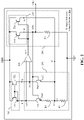
- FIG. 2 illustrates a schematic circuit diagram of the bandgap reference voltage generator 104 in accordance with an embodiment of the present disclosure.
- the bandgap reference voltage generator 104 can include a first current mirror circuit 202, a bandgap core circuit 204, an amplifier 206, and first feedback circuitry 208.
- the first current mirror circuit 202 can be coupled with the power supply 102, and configured to receive the supply voltage VDD, and output first and second currents 11 and 12.
- the first current mirror circuit 202 can include first and second transistors TS1 and TS2.
- the first and second transistors TS1 and TS2 have first terminals that can be coupled with the power supply 102, and configured to receive the supply voltage VDD. Second terminals of the first and second transistors TS1 and TS2 can be coupled with each other.
- the first transistor TS1 further has a third terminal that can be coupled with the second terminals of the first and second transistors TS1 and TS2, and configured to output the first current I1. Further, the second transistor TS2 has a third terminal that can be configured to output the second current 12.
- the first and second transistors TS1 and TS2 are p-channel metal-oxide semiconductor (PMOS) transistors, and the first through third terminals of the first and second transistors TS1 and TS2 correspond to source, gate, and drain terminals, respectively.
- PMOS metal-oxide semiconductor
- FIG. 2 illustrates that the third terminal of the first transistor TS1 is coupled with the second terminals of the first and second transistors TS1 and TS2 to form the first current mirror circuit 202
- the scope of the present disclosure is not limited to it.
- the third terminal of the second transistor TS2 may be coupled with the second terminals of the first and second transistors TS1 and TS2 to form the first current mirror circuit 202, without deviating from the scope of the present disclosure.
- the bandgap core circuit 204 can be coupled with the first current mirror circuit 202 ( i.e ., the third terminals of the first and second transistors TS1 and TS2), and configured to receive the first and second currents 11 and 12.
- the bandgap core circuit 204 can be further coupled with the first feedback circuitry 208, and configured to receive the bandgap reference voltage VBG and a third current 13. Based on the first through third currents 11-13 and the bandgap reference voltage VBG, the bandgap core circuit 204 can output first and second control voltages VC1 and VC2.
- the bandgap core circuit 204 can include third and fourth transistors TS3 and TS4, and first and second resistors R1 and R2.
- Each transistor of the third and fourth transistors TS3 and TS4 has first through third terminals.
- the first terminals of the third and fourth transistors TS3 and TS4 can be coupled with the third terminals of the first and second transistors TS1 and TS2, and configured to receive the first and second currents 11 and 12, respectively.
- the first terminals of the third and fourth transistors TS3 and TS4 can be further configured to output the first and second control voltages VC1 and VC2, respectively.
- the second terminals of the third and fourth transistors TS3 and TS4 can be coupled with the first feedback circuitry 208, and configured to receive the bandgap reference voltage VBG.
- the third and fourth transistors TS3 and TS4 are NPN transistors, and the first through third terminals of the third and fourth transistors TS3 and TS4 correspond to collector, base, and emitter terminals, respectively. Further, a size of the third transistor TS3 can be greater than a size of the fourth transistor TS4.
- base-emitter voltages can be generated at junctions between the second and third terminals of the third and fourth transistors TS3 and TS4.
- a first base-emitter voltage Vbe1 can be generated at a junction between the second and third terminals of the third transistor TS3.
- a second base-emitter voltage Vbe2 can be generated at a junction between the second and third terminals of the fourth transistor TS4.
- the first resistor R1 has first and second terminals coupled with the third terminals of the third and fourth transistors TS3 and TS4, respectively.
- third and fourth transistors TS3 and TS4 pass the first and second currents 11 and 12, respectively, in entirety (i.e., sans any drop).
- the first and second terminals of the first resistor R1 can be configured to receive the first and second currents 11 and 12, respectively.
- the second terminal of the first resistor R1 can be further coupled with the first feedback circuitry 208, and further configured to receive the third current 13. Further, it will be apparent to a person skilled in the art that a current passing through a resistor remains unchanged.
- the second terminal of the first resistor R1 receives the first through third currents 11-13.
- the first control voltage VC1 can thus be outputted based on the first and third currents 11 and 13 and the bandgap reference voltage VBG.
- the second control voltage VC2 can be outputted based on the second and third currents 12 and 13 and the bandgap reference voltage VBG.
- the second resistor R2 has a first terminal that can be coupled with the second terminal of the first resistor R1, and configured to receive a fourth current 14 and generate a first intermediate voltage VII.
- the fourth current 14 is equal to a sum of the first through third currents 11-13.
- the second resistor R2 further has a second terminal that can be coupled with the ground terminal.
- the bandgap reference voltage VBG is equal to a sum of the second base-emitter voltage Vbe2 of the fourth transistor TS4 and the first intermediate voltage VII.
- the amplifier 206 can be coupled with the first terminals of the third and fourth transistors TS3 and TS4, and the first feedback circuitry 208.
- the amplifier 206 can include suitable logic, circuitry, interfaces, and/or code, executable by the circuitry, that can be configured to perform one or more operations.
- the amplifier 206 can be configured to receive the first and second control voltages VC1 and VC2 from the first terminals of the third and fourth transistors TS3 and TS4, respectively.
- the amplifier 206 receives the first and second control voltages VC1 and VC2 at positive and negative input terminals thereof, respectively.
- the amplifier 206 can be further configured to generate a third control voltage VC3 based on the first and second control voltages VC1 and VC2, and provide the third control voltage VC3 to the first feedback circuitry 208.
- the third control voltage VC3 can be generated such that the third control voltage VC3 is greater than a difference between the first and second control voltages VC1 and VC2.
- the first feedback circuitry 208 can be coupled with the power supply 102, and configured to receive the supply voltage VDD.
- the first feedback circuitry 208 can be further coupled with the amplifier 206, and configured to receive the third control voltage VC3. Based on the supply voltage VDD and the third control voltage VC3, the first feedback circuitry 208 can be further configured to generate the bandgap reference voltage VBG. Further, the first feedback circuitry 208 can be configured to output the third current 13 based on the supply voltage VDD and the third control voltage VC3.
- the first feedback circuitry 208 can be further coupled with the bandgap core circuit 204, and further configured to provide the bandgap reference voltage VBG to the bandgap core circuit 204.
- the first feedback circuitry 208 can output the third current 13 such that the third current I3is sourced (i.e., provided) to the bandgap core circuit 204. Further, the first feedback circuitry 208 can be coupled with the functional circuit 106, and configured to provide the bandgap reference voltage VBG to the functional circuit 106.
- the first feedback circuitry 208 can include a first current replica circuit 210 and a third resistor R3.
- the first current replica circuit 210 can be coupled with the power supply 102, and configured to receive the supply voltage VDD.
- the first current replica circuit 210 can be further coupled with the amplifier 206, and configured to receive the third control voltage VC3. Further, the first current replica circuit 210 can be configured to output a fifth current 15 and the third current 13. The fifth and third currents 15 and 13 can thus be outputted based on the supply voltage VDD and the third control voltage VC3.
- the first current replica circuit 210 can include fifth and sixth transistors TS5 and TS6.
- the fifth and sixth transistors TS5 and TS6 have first terminals that can be coupled with the power supply 102, and configured to receive the supply voltage VDD.
- the fifth and sixth transistors TS5 and TS6 further have second terminals that can be coupled with the amplifier 206, and configured to receive the third control voltage VC3.
- the amplifier 206 can be coupled with the second terminals of the fifth and sixth transistors TS5 and TS6, and configured to provide the third control voltage VC3 to the second terminals of the fifth and sixth transistors TS5 and TS6.
- the fifth and sixth transistors TS5 and TS6 further have third terminals that can be configured to output the fifth and third currents 15 and 13, respectively.
- the fifth and sixth transistors TS5 and TS6 are PMOS transistors, and the first through third terminals of the fifth and sixth transistors TS5 and TS6 correspond to source, gate, and drain terminals, respectively.
- the first terminals (i.e., the source terminals) of the fifth and sixth transistors TS5 and TS6 are at a same voltage level (i.e., the supply voltage VDD).
- the second terminals (i.e., the gate terminals) of the fifth and sixth transistors TS5 and TS6 are at a same voltage level (i.e., the third control voltage VC3).
- the fifth and sixth transistors TS5 and TS6 form the first current replica circuit 210.
- sizes of the fifth and sixth transistors TS5 and TS6 are unequal.
- the third and fifth currents 13 and 15 are unequal.
- the third current 13 is a scaled down version of the fifth current 15.
- the third terminal of the sixth transistor TS6 can be coupled with the second terminal of the first resistor R1 (i.e., the bandgap core circuit 204), and output the third current 13 such that the third current 13 is sourced to the second terminal of the first resistor R1 ( i.e., the bandgap core circuit 204).
- the third resistor R3 has a first terminal that can be coupled with the ground terminal.
- the third resistor R3 further has a second terminal that can be coupled with the third terminal of the fifth transistor TS5 (i.e., the first current replica circuit 210), and configured to receive the fifth current 15 and generate the bandgap reference voltage VBG.
- the second terminal of the third resistor R3 can be further coupled with the second terminals of the third and fourth transistors TS3 and TS4, and further configured to provide the bandgap reference voltage VBG to the second terminals of the third and fourth transistors TS3 and TS4.
- the second terminals of the third and fourth transistors TS3 and TS4 can be configured to receive the bandgap reference voltage VBG from the second terminal of the third resistor R3. Further, the second terminal of the third resistor R3 can be coupled with the functional circuit 106, and configured to provide the bandgap reference voltage VBG to the functional circuit 106.
- the bandgap reference voltage VBG can be generated at the second terminal of the third resistor R3, the scope of the present disclosure is not limited to it.
- the third resistor R3 can be split into various segments and the bandgap reference voltage VBG can be generated at any intermediate terminal of such segments, without deviating from the scope of the present disclosure. In such a scenario, a sum of resistance values of the segments is equal to a resistance value of the third resistor R3.
- the bandgap reference voltage VBG is equal to a sum of the second base-emitter voltage Vbe2 of the fourth transistor TS4 and the first intermediate voltage VII.
- the threshold value i.e., the bandgap reference voltage at 0 K.
- the amplifier 206 and the first feedback circuitry 208 form a negative feedback loop with respect to the first current mirror circuit 202 and the bandgap core circuit 204. Such a negative feedback loop results in the first current 11 being equal to the second current 12.
- the size of the third transistor TS3 is greater than that of the fourth transistor TS4
- the first base-emitter voltage Vbe1 of the third transistor TS3 is less than the second base-emitter voltage Vbe2 of the fourth transistor TS4.
- the difference between the first and second base-emitter voltages Vbe1 and Vbe2 is generated across the first resistor R1.
- the first terminal of the third resistor R3 receives the fifth current 15 and generates the bandgap reference voltage VBG.
- the third current 13 is a scaled down version of the fifth current 15. For the sake of ongoing discussion, it is assumed that the third current 13 is "k1" times the fifth current 15, where "k1" is a first scaling factor and is less than one.
- the first intermediate voltage VII is generated based on the fourth current 14.
- the bandgap reference voltage VBG is equal to the sum of the second base-emitter voltage Vbe2 of the fourth transistor TS4 and the first intermediate voltage VII.
- the difference between the first and second base-emitter voltages Vbe1 and Vbe2 has a positive temperature co-efficient, whereas the second base-emitter voltage Vbe2 has a negative temperature co-efficient.
- a temperature-independent bandgap reference voltage VBG may be generated.
- a current density of a transistor is inversely proportional to a size of the transistor.
- the bandgap reference voltage VBG is thus greater than the bandgap reference voltage at 0 K (i.e., the threshold value).
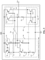
- FIG. 3 illustrates a schematic circuit diagram of the bandgap reference voltage generator 104 in accordance with another embodiment of the present disclosure.
- the bandgap reference voltage generator 104 can include the first current mirror circuit 202, the bandgap core circuit 204, the amplifier 206, and second feedback circuitry 302.
- the first current mirror circuit 202 can be coupled with the power supply 102, and configured to receive the supply voltage VDD, and output first and second currents 11 and 12.
- the first current mirror circuit 202 can include the first and second transistors TS1 and TS2.
- the first terminals of the first and second transistors TS1 and TS2 can be coupled with the power supply 102, and configured to receive the supply voltage VDD, and the second terminals of the first and second transistors TS1 and TS2 can be coupled with each other.
- the third terminal of the first transistor TS1 can be coupled with the second terminals of the first and second transistors TS1 and TS2, and configured to output the first current I1. Further, the third terminal of the second transistor TS2 can be configured to output the second current 12.
- the bandgap core circuit 204 can be coupled with the first current mirror circuit 202, and configured to receive the first and second currents 11 and 12.
- the bandgap core circuit 204 can be further coupled with the second feedback circuitry 302, and configured to receive the bandgap reference voltage VBG. Further, the coupling between the bandgap core circuit 204 and the second feedback circuitry 302 can be such that a sixth current 16 outputted by the second feedback circuitry 302 is sank from the bandgap core circuit 204.
- the bandgap core circuit 204 Based on the first, second, and sixth currents I1, 12, and 16 and the bandgap reference voltage VBG, the bandgap core circuit 204 can be further configured to output fourth and fifth control voltages VC4 and VC5.
- the bandgap core circuit 204 can include the third and fourth transistors TS3 and TS4, and the first and second resistors R1 and R2.
- the first terminals of the third and fourth transistors TS3 and TS4 can be coupled with the third terminals of the first and second transistors TS1 and TS2, and configured to receive the first and second currents 11 and 12, respectively.
- the first terminals of the third and fourth transistors TS3 and TS4 can be further configured to output the fourth and fifth control voltages VC4 and VC5, respectively.
- the second terminals of the third and fourth transistors TS3 and TS4 can be coupled with the second feedback circuitry 302, and configured to receive the bandgap reference voltage VBG.
- the first and second terminals of the first resistor R1 can be coupled with the third terminals of the third and fourth transistors TS3 and TS4, and configured to receive the first and second currents 11 and 12, respectively.
- the second terminal of the first resistor R1 can be further coupled with the second feedback circuitry 302.
- the coupling of the second terminal of the first resistor R1 and the second feedback circuitry 302 can be such that the sixth current 16 outputted by the second feedback circuitry 302 is sank from the second terminal of the first resistor R1.
- the fourth control voltage VC4 can thus be outputted based on the first and sixth currents 11 and 16 and the bandgap reference voltage VBG.
- the fifth control voltage VC5 can be outputted based on the second and sixth currents 12 and 16 and the bandgap reference voltage VBG.
- the first terminal of the second resistor R2 can be coupled with the second terminal of the first resistor R1, and configured to receive a seventh current 17 and generate a second intermediate voltage VI2.
- the seventh current 17 can be equal to a difference between the sixth current 16 and a sum of the first and second currents 11 and 12.
- the second resistor R2 further has a second terminal that can be coupled with the ground terminal.
- the bandgap reference voltage VBG can be equal to a sum of the second base-emitter voltage Vbe2 of the fourth transistor TS4 and the second intermediate voltage VI2.
- the amplifier 206 can be coupled with the first terminals of the third and fourth transistors TS3 and TS4, and the second feedback circuitry 302.
- the amplifier 206 can be configured to receive the fourth and fifth control voltages VC4 and VC5 from the first terminals of the third and fourth transistors TS3 and TS4, respectively.
- the amplifier 206 receives the fourth and fifth control voltages VC4 and VC5 at positive and negative input terminals thereof, respectively.
- the amplifier 206 can be further configured to generate a sixth control voltage VC6 based on the fourth and fifth control voltages VC4 and VC5, and provide the sixth control voltage VC6 to the second feedback circuitry 302.
- the sixth control voltage VC6 can be generated such that the sixth control voltage VC6 can be greater than a difference between the fourth and fifth control voltages VC4 and VC5.
- the second feedback circuitry 302 can be coupled with the power supply 102, and configured to receive the supply voltage VDD.
- the second feedback circuitry 302 can be further coupled with the amplifier 206, and configured to receive the sixth control voltage VC6. Based on the supply voltage VDD and the sixth control voltage VC6, the second feedback circuitry 302 can be further configured to generate the bandgap reference voltage VBG.
- the second feedback circuitry 302 can be further configured to output the sixth current 16 based on the supply voltage VDD and the sixth control voltage VC6.
- the second feedback circuitry 302 can be further coupled with the bandgap core circuit 204, and further configured to provide the bandgap reference voltage VBG to the bandgap core circuit 204.
- the second feedback circuitry 302 can output the sixth current 16 such that the sixth current 16 is sank from the bandgap core circuit 204.
- the second feedback circuitry 302 can be further coupled with the functional circuit 106, and further configured to provide the bandgap reference voltage VBG to the functional circuit 106.
- the second feedback circuitry 302 can include a second current replica circuit 304, a fourth resistor R4, and a second current mirror circuit 306.
- the second current replica circuit 304 can be coupled with the power supply 102, and configured to receive the supply voltage VDD.
- the second current replica circuit 304 can be further coupled with the amplifier 206, and configured to receive the sixth control voltage VC6. Further, the second current replica circuit 304 can be configured to output eighth and ninth currents 18 and 19. The eighth and ninth currents 18 and 19 can thus be outputted based on the supply voltage VDD and the sixth control voltage VC6.
- the second current replica circuit 304 can include seventh and eighth transistors TS7 and TS8.
- the seventh and eighth transistors TS7 and TS8 have first terminals that can be coupled with the power supply 102, and configured to receive the supply voltage VDD.
- the seventh and eighth transistors TS7 and TS8 further have second terminals that can be coupled with the amplifier 206, and configured to receive the sixth control voltage VC6.
- the amplifier 206 can be coupled with the second terminals of the seventh and eighth transistors TS7 and TS8, and configured to provide the sixth control voltage VC6 to the second terminals of the seventh and eighth transistors TS7 and TS8.
- the seventh and eighth transistors TS7 and TS8 further have third terminals that can be configured to output the eighth and ninth currents 18 and 19, respectively.
- the eighth and ninth currents 18 and 19 can thus be outputted based on the supply voltage VDD and the sixth control voltage VC6.
- the seventh and eighth transistors TS7 and TS8 are PMOS transistors, and the first through third terminals of the seventh and eighth transistors TS7 and TS8 correspond to source, gate, and drain terminals, respectively.
- the first terminals (i.e., the source terminals) of the seventh and eighth transistors TS7 and TS8 are at a same voltage level (i.e., the supply voltage VDD).
- the second terminals (i.e., the gate terminals) of the seventh and eighth transistors TS7 and TS8 are at a same voltage level (i.e., the sixth control voltage VC6).
- the seventh and eighth transistors TS7 and TS8 form the second current replica circuit 304.
- sizes of the seventh and eighth transistors TS7 and TS8 are unequal.
- the eighth and ninth currents 18 and 19 are unequal.
- the ninth current 19 is a scaled down version of the eighth current 18.
- the second current mirror circuit 306 can be coupled with the third terminal of the eighth transistor TS8 (i.e., the second current replica circuit 304), and configured to receive the ninth current 19. Further, the second current mirror circuit 306 can be coupled with the bandgap core circuit 204, and configured to output, based on the ninth current 19, the sixth current 16 such that the sixth current 16 is sank from the bandgap core circuit 204.
- the second current mirror circuit 306 can include ninth and tenth transistors TS9 and TS10.
- the ninth and tenth transistors TS9 and TS10 have first terminals that can be coupled with the ground terminal, and second terminals that can be coupled with each other.
- the ninth transistor TS9 further has a third terminal that can be coupled with the second terminals of the ninth and tenth transistors TS9 and TS10 and the third terminal of the eighth transistor TS8, and configured to receive the ninth current 19.
- the tenth transistor TS10 further has a third terminal that can be coupled with the second terminal of the first resistor R1, and configured to output the sixth current 16 such that the sixth current 16 is sank from the second terminal of the first resistor R1.
- the ninth and tenth transistors TS9 and TS10 are n-channel metal-oxide semiconductor (NMOS) transistors, and the first through third terminals of the ninth and tenth transistors TS9 and TS10 correspond to source, gate, and drain terminals, respectively.
- NMOS metal-oxide semiconductor
- the sixth current 16 is equal to the ninth current 19.
- the scope of the present disclosure is not limited to the mirroring ratio of the second current mirror circuit 306 being one. In various other embodiments, the mirroring ratio of the second current mirror circuit 306 can be less than or greater than one, without deviating from the scope of the present disclosure.
- the fourth resistor R4 has a first terminal that can be coupled with the ground terminal.
- the fourth resistor R4 further has a second terminal that can be coupled with the third terminal of the seventh transistor TS7 (i.e., the second current replica circuit 304), and configured to receive the eighth current 18 and generate the bandgap reference voltage VBG.
- the second terminal of the fourth resistor R4 can be further coupled with the second terminals of the third and fourth transistors TS3 and TS4, and configured to provide the bandgap reference voltage VBG to the second terminals of the third and fourth transistors TS3 and TS4.
- the second terminals of the third and fourth transistors TS3 and TS4 can be configured to receive the bandgap reference voltage VBG from the second terminal of the fourth resistor R4. Further, the second terminal of the fourth resistor R4 can be coupled with the functional circuit 106, and configured to provide the bandgap reference voltage VBG to the functional circuit 106.
- the bandgap reference voltage VBG is generated at the second terminal of the fourth resistor R4, the scope of the present disclosure is not limited to it.
- the fourth resistor R4 can be split into various segments and the bandgap reference voltage VBG can be generated at any intermediate terminal of such segments, without deviating from the scope of the present disclosure. In such a scenario, a sum of resistance values of the segments is equal to a resistance value of the fourth resistor R4.
- the bandgap reference voltage VBG is equal to a sum of the second base-emitter voltage Vbe2 of the fourth transistor TS4 and the second intermediate voltage VI2.
- the threshold value i.e., the bandgap reference voltage at 0 K.
- the amplifier 206 and the second feedback circuitry 302 form a negative feedback loop with respect to the first current mirror circuit 202 and the bandgap core circuit 204. Such a negative feedback loop results in the first current 11 being equal to the second current 12.
- the size of the third transistor TS3 is greater than that of the fourth transistor TS4
- the first base-emitter voltage Vbe1 of the third transistor TS3 is less than the second base-emitter voltage Vbe2 of the fourth transistor TS4.
- the difference between the first and second base-emitter voltages Vbe1 and Vbe2 is generated across the first resistor R1.
- the first terminal of the fourth resistor R4 receives the eighth current 18 and generates the bandgap reference voltage VBG.
- the ninth current 19 is a scaled down version of the eighth current 18. For the sake of ongoing discussion, it is assumed that the ninth current is "k2" times the eighth current 18, where "k2" is a second scaling factor and is less than one.
- the second intermediate voltage VI2 is generated based on the seventh current 17.
- the seventh current 17 is equal to a difference between the sixth current 16 and the sum of the first and second currents 11 and 12. Further, the first and second currents 11 and 12 are equal and the sixth current 16 is equal to the ninth current 19.
- the bandgap reference voltage VBG is equal to the sum of the second base-emitter voltage Vbe2 of the fourth transistor TS4 and the second intermediate voltage VI2.
- the difference between the first and second base-emitter voltages Vbe1 and Vbe2 has a positive temperature co-efficient, whereas the second base-emitter voltage Vbe2 has a negative temperature co-efficient.
- a temperature-independent bandgap reference voltage VBG can be generated.
- Vbe 2 V bg 0 + T T 0
- equation (23) is obtained as shown below:
- VBG V bg 0 + T T 0
- the bandgap reference voltage VBG is thus less than the bandgap reference voltage at 0 K (i.e., the threshold value).
- FIG. 4A illustrates a schematic circuit diagram of the bandgap reference voltage generator 104 in accordance with yet another embodiment of the present disclosure.
- the bandgap reference voltage generator 104 can include the first current mirror circuit 202, the bandgap core circuit 204, the amplifier 206, and third feedback circuitry 402.
- the first current mirror circuit 202 can be coupled with the power supply 102, and configured to receive the supply voltage VDD, and output the first and second currents 11 and 12.
- the first current mirror circuit 202 can include the first and second transistors TS1 and TS2.
- the first terminals of the first and second transistors TS1 and TS2 can be coupled with the power supply 102, and configured to receive the supply voltage VDD, and the second terminals of the first and second transistors TS1 and TS2 can be coupled with each other.
- the third terminal of the first transistor TS1 can be coupled with the second terminals of the first and second transistors TS1 and TS2, and configured to output the first current I1. Further, the third terminal of the second transistor TS2 can be configured to output the second current 12.
- the bandgap core circuit 204 can be coupled with the first current mirror circuit 202, and configured to receive the first and second currents 11 and 12.
- the bandgap core circuit 204 can be further coupled with the third feedback circuitry 402, and configured to receive the bandgap reference voltage VBG and a tenth current 110. Based on the first, second, and tenth currents I1, 12, and 110 and the bandgap reference voltage VBG, the bandgap core circuit 204 can be further configured to output seventh and eighth control voltages VC7 and VC8.
- the bandgap core circuit 204 can include the third and fourth transistors TS3 and TS4, and the first and second resistors R1 and R2.
- the first terminals of the third and fourth transistors TS3 and TS4 can be coupled with the first current mirror circuit 202, and configured to receive the first and second currents 11 and 12, respectively.
- the first terminals of the third and fourth transistors TS3 and TS4 can be further configured to output the seventh and eighth control voltages VC7 and VC8, respectively.
- the second terminals of the third and fourth transistors TS3 and TS4 can be coupled with the third feedback circuitry 402, and configured to receive the bandgap reference voltage VBG.
- the first and second terminals of the first resistor R1 can be coupled with the third terminals of the third and fourth transistors TS3 and TS4, and configured to receive the first and second currents 11 and 12, respectively.
- the second terminal of the first resistor R1 can be further coupled with the third feedback circuitry 402, and further configured to receive the tenth current 110.
- the seventh control voltage VC7 can thus be outputted based on the first and tenth currents 11 and 110 and the bandgap reference voltage VBG.
- the eighth control voltage VC8 can be outputted based on the second and tenth currents 12 and 110 and the bandgap reference voltage VBG.
- the first terminal of the second resistor R2 can be coupled with the second terminal of the first resistor R1, and configured to receive an eleventh current 111 and generate a third intermediate voltage VI3.
- the eleventh current 111 is equal to a sum of the first, second, and tenth currents I1, I2, and 110.
- the second terminal of the second resistor R2 can be coupled with the ground terminal.
- the bandgap reference voltage VBG is equal to a sum of the second base-emitter voltage Vbe2 of the fourth transistor TS4 and the third intermediate voltage VI3.
- the amplifier 206 can be coupled with the first terminals of the third and fourth transistors TS3 and TS4, and the third feedback circuitry 402.
- the amplifier 206 can be configured to receive the seventh and eighth control voltages VC7 and VC8 from the first terminals of the third and fourth transistors TS3 and TS4, respectively.
- the amplifier 206 receives the seventh and eighth control voltages VC7 and VC8 at positive and negative input terminals thereof, respectively.
- the amplifier 206 can be further configured to generate a ninth control voltage VC9 based on the seventh and eighth control voltages VC7 and VC8, and provide the ninth control voltage VC9 to the third feedback circuitry 402.
- the ninth control voltage VC9 can be generated such that the ninth control voltage VC9 can be greater than a difference between the seventh and eighth control voltages VC7 and VC8.
- the third feedback circuitry 402 can be coupled with the power supply 102, and configured to receive the supply voltage VDD.
- the third feedback circuitry 402 can be further coupled with the amplifier 206, and configured to receive the ninth control voltage VC9. Based on the supply voltage VDD and the ninth control voltage VC9, the third feedback circuitry 402 can be further configured to generate the bandgap reference voltage VBG and the tenth current 110 based on the supply voltage VDD and the ninth control voltage VC9. Further, the third feedback circuitry 402 can be coupled with the bandgap core circuit 204, and configured to provide the bandgap reference voltage VBG and the tenth current 110 to the bandgap core circuit 204.
- the third feedback circuitry 402 can be further coupled with the functional circuit 106, and further configured to provide the bandgap reference voltage VBG to the functional circuit 106.
- the third feedback circuitry 402 can include an eleventh transistor TS11 and a fifth resistor R5.
- the eleventh transistor TS11 has a first terminal that can be coupled with the power supply 102, and configured to receive the supply voltage VDD.
- the eleventh transistor TS11 further has a second terminal that can be coupled with the amplifier 206, and configured to receive the ninth control voltage VC9.
- the amplifier 206 can be coupled with the second terminal of the eleventh transistor TS11, and configured to provide the ninth control voltage VC9 to the second terminal of the eleventh transistor TS11.
- the eleventh transistor TS11 further has a third terminal that can be configured to output a twelfth current 112.
- the twelfth current 112 can thus be outputted based on the supply voltage VDD and the ninth control voltage VC9.
- the eleventh transistor TS11 is a PMOS transistor, and the first through third terminals of the eleventh transistor TS11 correspond to source, gate, and drain terminals, respectively.
- the fifth resistor R5 has a first terminal that can be coupled with the third terminal of the eleventh transistor TS11, and configured to receive the twelfth current 112 and generate the bandgap reference voltage VBG.
- the first terminal of the fifth resistor R5 can be further coupled with the second terminals of the third and fourth transistors TS3 and TS4, and configured to provide the bandgap reference voltage VBG to the second terminals of the third and fourth transistors TS3 and TS4.
- the second terminals of the third and fourth transistors TS3 and TS4 can be configured to receive the bandgap reference voltage VBG from the first terminal of the fifth resistor R5.
- the first terminal of the fifth resistor R5 can be further coupled with the functional circuit 106, and configured to provide the bandgap reference voltage VBG to the functional circuit 106.
- the fifth resistor R5 further has a second terminal that can be coupled with the bandgap core circuit 204 (i.e., the second terminal of the first resistor R1), and configured to generate and provide the tenth current 110 to the second terminal of the first resistor R1.
- the tenth and twelfth currents 110 and 112 are equal.
- the bandgap reference voltage VBG is equal to a sum of the second base-emitter voltage Vbe2 of the fourth transistor TS4 and the third intermediate voltage VI3.
- the threshold value i.e., the bandgap reference voltage at 0 K.
- the amplifier 206 and the third feedback circuitry 402 form a negative feedback loop with respect to the first current mirror circuit 202 and the bandgap core circuit 204. Such a negative feedback loop results in the first current 11 being equal to the second current 12.
- the size of the third transistor TS3 is greater than that of the fourth transistor TS4
- the first base-emitter voltage Vbe1 of the third transistor TS3 is less than the second base-emitter voltage Vbe2 of the fourth transistor TS4.
- the difference between the first and second base-emitter voltages Vbe1 and Vbe2 is generated across the first resistor R1.
- the third intermediate voltage VI3 is generated based on the eleventh current I11.
- the eleventh current 111 is equal to the sum of the first, second, and tenth currents I1, 12, and 110. Further, the first and second currents 11 and 12 are equal.
- the bandgap reference voltage VBG is equal to the sum of the second base-emitter voltage Vbe2 of the fourth transistor TS4 and the third intermediate voltage VI3.
- Vbe 2 V bg 0 + T T 0
- the bandgap reference voltage VBG is thus greater than the bandgap reference voltage at 0 K (i.e., the threshold value).
- the bandgap reference voltage VBG generated by the bandgap reference voltage generator 104 of FIG. 4A is temperature-dependent.
- FIG. 4A describes that the bandgap reference voltage VBG is generated at the first terminal of the fifth resistor R5, the scope of the present disclosure is not limited to it.
- the bandgap reference voltage VBG can be generated at the second terminal of the fifth resistor R5, without deviating from the scope of the present disclosure.
- the bandgap reference voltage VBG is less than the bandgap reference voltage at 0 K (i.e., the threshold value).
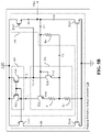
- FIG. 4B illustrates a schematic circuit diagram of the bandgap reference voltage generator 104 in accordance with yet another embodiment of the present disclosure.
- the bandgap reference voltage generator 104 can include the first current mirror circuit 202, the bandgap core circuit 204, and fourth feedback circuitry 404.
- the structure and functionalities of the first current mirror circuit 202 and the bandgap core circuit 204 remain same as described in FIG. 4A .
- the difference between the embodiments of FIG. 4A and FIG. 4B is in the absence of the amplifier 206.
- the third feedback circuitry 402 i.e., the second terminal of the eleventh transistor TS11
- the first terminal of the fourth transistor TS4 can be directly coupled with the second terminal of the eleventh transistor TS11, and configured to provide the eighth control voltage VC8 to the second terminal of the eleventh transistor TS11.
- the fourth feedback circuitry 404 is functionally similar to the third feedback circuitry 402.
- the difference between the third and fourth feedback circuitries 402 and 404 is that the PMOS transistor of the third feedback circuitry 402 (i.e., the eleventh transistor TS11) is replaced by an NMOS transistor (i.e., a twelfth transistor TS12) in the fourth feedback circuitry 404.
- the twelfth transistor TS12 can be configured to output a thirteenth current 113 based on the supply voltage VDD and the eighth control voltage VC8.
- the first and second terminals of the fifth resistor R5 can then be configured to generate the bandgap reference voltage VBG and a fourteenth current 114, respectively, based on the thirteenth current 113 in a similar manner as described above in FIG. 4A .
- the bandgap reference voltage VBG and the fourteenth current 114 can then be provided to the bandgap core circuit 204 to facilitate the generation of the eighth control voltage VC8.
- FIG. 5A illustrates a schematic circuit diagram of the bandgap reference voltage generator 104 in accordance with yet another embodiment of the present disclosure.
- the bandgap reference voltage generator 104 can include the first current mirror circuit 202, the bandgap core circuit 204, the amplifier 206, and fifth feedback circuitry 502.
- the first current mirror circuit 202 can be coupled with the power supply 102, and configured to receive the supply voltage VDD, and output the first and second currents 11 and 12.
- the first current mirror circuit 202 can include the first and second transistors TS1 and TS2.
- the first terminals of the first and second transistors TS1 and TS2 can be coupled with the power supply 102, and configured to receive the supply voltage VDD, and the second terminals of the first and second transistors TS1 and TS2 can be coupled with each other.
- the third terminal of the first transistor TS1 can be coupled with the second terminals of the first and second transistors TS1 and TS2, and configured to output the first current I1. Further, the third terminal of the second transistor TS2 can be configured to output the second current 12.
- the bandgap core circuit 204 can be coupled with the first current mirror circuit 202, and configured to receive the first and second currents 11 and 12.
- the bandgap core circuit 204 can be further coupled with the fifth feedback circuitry 502, and configured to receive the bandgap reference voltage VBG and a fifteenth current 115. Based on the first, second, and fifteenth currents I1, I2, and 115 and the bandgap reference voltage VBG, the bandgap core circuit 204 can be further configured to output tenth and eleventh control voltages VC10 and VC11.
- the bandgap core circuit 204 can include the third and fourth transistors TS3 and TS4, and the first and second resistors R1 and R2.
- the first terminals of the third and fourth transistors TS3 and TS4 can be coupled with the third terminals of the first and second transistors TS1 and TS2, and configured to receive the first and second currents 11 and 12, respectively.
- the first terminals of the third and fourth transistors TS3 and TS4 can be further configured to output the tenth and eleventh control voltages VC10 and VC11, respectively.
- the second terminals of the third and fourth transistors TS3 and TS4 can be coupled with the fifth feedback circuitry 502, and configured to receive the bandgap reference voltage VBG.
- the first and second terminals of the first resistor R1 can be coupled with the third terminals of the third and fourth transistors TS3 and TS4, and configured to receive the first and second currents 11 and 12, respectively. Further, the second terminal of the first resistor R1 can be coupled with the fifth feedback circuitry 502, and configured to receive the fifteenth current 115. Thus, the second terminal of the first resistor R1 can receive the first, second, and fifteenth currents I1, I2, and I15.
- the tenth control voltage VC10 can thus be outputted based on the first and fifteenth currents 11 and 115 and the bandgap reference voltage VBG. Similarly, the eleventh control voltage VC11 can be outputted based on the second and fifteenth currents 12 and 115 and the bandgap reference voltage VBG.
- the first terminal of the second resistor R2 can be coupled with the second terminal of the first resistor R1, and configured to receive a sixteenth current 116 and generate a fourth intermediate voltage VI4.
- the fourteenth current 114 is equal to a sum of the first, second, and fifteenth currents I1, I2, and 115.
- the second terminal of the second resistor R2 can be coupled with the ground terminal.
- the bandgap reference voltage VBG is equal to a sum of the second base-emitter voltage Vbe2 of the fourth transistor TS4 and the fourth intermediate voltage VI4.
- the amplifier 206 can be coupled with the first terminals of the third and fourth transistors TS3 and TS4, and the fifth feedback circuitry 502.
- the amplifier 206 can be configured to receive the tenth and eleventh control voltages VC10 and VC11 from the first terminals of the third and fourth transistors TS3 and TS4, respectively.
- the amplifier 206 receives the tenth and eleventh control voltages VC10 and VC11 at positive and negative input terminals thereof, respectively.
- the amplifier 206 can be further configured to generate a twelfth control voltage VC12 based on the tenth and eleventh control voltages VC10 and VC11, and provide the twelfth control voltage VC12 to the fifth feedback circuitry 502.
- the twelfth control voltage VC12 can be generated such that the twelfth control voltage VC12 can be greater than a difference between the tenth and eleventh control voltages VC10 and VC11.
- the fifth feedback circuitry 502 can be coupled with the power supply 102, and configured to receive the supply voltage VDD.
- the fifth feedback circuitry 502 can be further coupled with the amplifier 206, and configured to receive the twelfth control voltage VC12. Based on the supply voltage VDD and the twelfth control voltage VC12, the fifth feedback circuitry 502 can be further configured to generate the bandgap reference voltage VBG and the fifteenth current 115.
- the fifth feedback circuitry 502 can be further coupled with the bandgap core circuit 204, and further configured to provide the bandgap reference voltage VBG and the fifteenth current 115 to the bandgap core circuit 204.
- the fifth feedback circuitry 502 can be coupled with the functional circuit 106, and configured to provide the bandgap reference voltage VBG to the functional circuit 106.
- the fifth feedback circuitry 502 can include thirteenth through sixteenth transistors TS12-TS15 and a sixth resistor R6.
- the sixth resistor R6 has a first terminal that can be configured to receive a seventeenth current 117, and generate the bandgap reference voltage VBG.
- the first terminal of the sixth resistor R6 can be further coupled with the second terminals of the third and fourth transistors TS3 and TS4, and configured to provide the bandgap reference voltage VBG to the second terminals of the third and fourth transistors TS3 and TS4.
- the second terminals of the third and fourth transistors TS3 and TS4 can be configured to receive the bandgap reference voltage VBG from the first terminal of the sixth resistor R6.
- the first terminal of the sixth resistor R6 can be further coupled with the functional circuit 106, and configured to provide the bandgap reference voltage VBG to the functional circuit 106.
- the sixth resistor R6 further has a second terminal that can be coupled with the bandgap core circuit 204 (i.e., the second terminal of the first resistor R1), and configured to generate and provide the fifteenth current 115 to the second terminal of the first resistor R1. In one embodiment, the fifteenth and seventeenth currents 115 and 117 are equal.
- the thirteenth transistor TS13 has first through third terminals.
- the first terminal of the thirteenth transistor TS13 can be coupled with the power supply 102, and configured to receive the supply voltage VDD.
- the second terminal of the thirteenth transistor TS13 can be coupled with the first current mirror circuit 202 (i.e., the second terminals of the first and second transistors TS1 and TS2), and the third terminal of the thirteenth transistor TS13 can be configured to output an eighteenth current 118.
- the thirteenth transistor TS13 is a PMOS transistor, and the first through third terminals of the thirteenth transistor TS13 correspond to source, gate, and drain terminals, respectively.
- the first terminals (i.e., the source terminals) of the first and thirteenth transistors TS1 and TS13 are at a same voltage level (i.e., the supply voltage VDD).
- the second terminals (i.e., the gate terminals) of the first and thirteenth transistors TS1 and TS13 are at a same voltage level.
- the first and thirteenth transistors TS1 and TS13 form a third current replica circuit (not shown).
- sizes of the first and thirteenth transistors TS1 and TS13 are unequal.
- the first and eighteenth currents 11 and 118 are unequal.
- the eighteenth current 118 is a scaled down version of the first current I1.
- the fourteenth transistor TS14 has first through third terminals.
- the first terminal of the fourteenth transistor TS14 can be coupled with the ground terminal.
- the third terminal of the fourteenth transistor TS14 can be coupled with the third terminal of the thirteenth transistor TS13, and configured to receive the eighteenth current 118.
- the fourteenth transistor TS14 is an NMOS transistor, and the first through third terminals of the fourteenth transistor TS14 correspond to source, gate, and drain terminals, respectively.
- the fifteenth transistor TS15 has first through third terminals.
- the first terminal of the fifteenth transistor TS15 can be coupled with the ground terminal, and the second terminal of the fifteenth transistor TS15 can be coupled with the second terminal of the fourteenth transistor TS14.
- the third terminal of the fifteenth transistor TS15 can be coupled with the first terminal of the sixth resistor R6, and configured to output a nineteenth current 119 such that the nineteenth current 119 is sank from the first terminal of the sixth resistor R6.
- the fifteenth transistor TS15 is an NMOS transistor, and the first through third terminals of the fifteenth transistor TS15 correspond to source, gate, and drain terminals, respectively.
- the nineteenth current 119 is equal to the eighteenth current 118.
- the scope of the present disclosure is not limited to the nineteenth current 119 being equal to the eighteenth current 118.
- the nineteenth current 119 can be a scaled down version of the eighteenth current 118, without deviating from the scope of the present disclosure.
- the sixteenth transistor TS16 has a first terminal that can be coupled with the power supply 102, and configured to receive the supply voltage VDD.
- the sixteenth transistor TS16 further has a second terminal that can be coupled with the amplifier 206, and configured to receive the twelfth control voltage VC12.
- the amplifier 206 can be coupled with the second terminal of the sixteenth transistor TS16, and configured to provide the twelfth control voltage VC12 to the second terminal of the sixteenth transistor TS16.
- the sixteenth transistor TS16 further has a third terminal that can be coupled with the third terminal of the fifteenth transistor TS15 and the first terminal of the sixth resistor R6, and configured to output a twentieth current 120.
- the sixteenth transistor TS16 is a PMOS transistor, and the first through third terminals of the sixteenth transistor TS16 correspond to source, gate, and drain terminals, respectively.
- the twentieth current 120 can be thus outputted based on the supply voltage VDD and the twelfth control voltage VC12.
- the third terminal of the sixteenth transistor TS16 can output the twentieth current 120 such that the twentieth current 120 is sourced to the first terminal of the sixth resistor R6.
- the seventeenth current 117 received by the first terminal of the sixth resistor R6 can thus be generated based on the nineteenth and twentieth currents 119 and 120. In other words, the seventeenth current 117 is equal to a difference between the nineteenth and twentieth currents 119 and 120.
- the bandgap reference voltage VBG is equal to a sum of the second base-emitter voltage Vbe2 of the fourth transistor TS4 and the fourth intermediate voltage VI4.
- the threshold value i.e., the bandgap reference voltage at 0 K.
- FIG. 5B illustrates a schematic circuit diagram of the bandgap reference voltage generator 104 in accordance with yet another embodiment of the present disclosure.
- the bandgap reference voltage generator 104 can include the first current mirror circuit 202, the bandgap core circuit 204, and sixth feedback circuitry 504.
- the sixth feedback circuitry 504 (i.e., the second terminal of the sixteenth transistor TS16) receives the eleventh control voltage VC11, as compared to the twelfth control voltage VC12 as described in FIG. 5A .
- the first terminal of the fourth transistor TS4 is directly coupled with the second terminal of the sixteenth transistor TS16, and configured to provide the eleventh control voltage VC11 to the second terminal of the sixteenth transistor TS16.
- the sixth feedback circuitry 504 is functionally similar to the fifth feedback circuitry 502.
- the difference between the fifth and sixth feedback circuitries 502 and 504 is that the PMOS transistor of the fifth feedback circuitry 502 (i.e., the sixteenth transistor TS16) is replaced by an NMOS transistor (i.e., a seventeenth transistor TS17) in the sixth feedback circuitry 504.
- the seventeenth transistor TS17 can be configured to output a twenty-first current 121 based on the supply voltage VDD and the eleventh control voltage VC11.
- the first terminal of the sixth resistor R6 can then receive a twenty-second current 122 that is outputted based on the nineteenth and twenty-first currents 119 and 121 (i.e., is equal to a difference between the nineteenth and twenty-first currents 119 and 121). Further, the first and second terminals of the sixth resistor R6 can then be configured to generate the bandgap reference voltage VBG and a twenty-third current 123, respectively, based on the twenty-second current 122 in a similar manner as described above in FIG. 5A . The bandgap reference voltage VBG and the twenty-third current 123 can then be provided to the bandgap core circuit 204 to facilitate the generation of the eleventh control voltage VC11.
- the bandgap reference voltage generator 104 of the present disclosure generates the bandgap reference voltage VBG having a voltage level that can be greater than or less than a bandgap reference voltage at 0 K.
- a bandgap reference voltage VBG is generated by utilizing exclusively feedback circuitry (such as the first through sixth feedback circuitries 208, 302, 402, 404, 502, and 504) and sans any additional circuits (i.e., circuits that are not included in the feedback loop with the bandgap core circuit 204 and the first current mirror circuit 202).
- a power supply rejection ratio of the bandgap reference voltage generator 104 of the present disclosure is greater than that of a conventional bandgap reference voltage generator that has significant base currents being generated in bipolar transistors of a corresponding bandgap core circuit, and hence, is required to implement various current compensation circuits therein.
- a size and a manufacturing cost of the bandgap reference voltage generator 104 are significantly less than that of the conventional bandgap reference voltage generator.
- a power consumed by the bandgap reference voltage generator 104 is significantly less than that consumed by the conventional bandgap reference voltage generator.
Landscapes
- Engineering & Computer Science (AREA)
- Physics & Mathematics (AREA)
- Electromagnetism (AREA)
- General Physics & Mathematics (AREA)
- Radar, Positioning & Navigation (AREA)
- Automation & Control Theory (AREA)
- Microelectronics & Electronic Packaging (AREA)
- Power Engineering (AREA)
- Nonlinear Science (AREA)
- Control Of Electrical Variables (AREA)
Abstract
Description
- The present disclosure relates generally to electronic circuits, and, more particularly, to a bandgap reference voltage generator.
- System-on-chips (SoC) include various bandgap reference voltage generators that generate bandgap reference voltages. The generated bandgap reference voltages are utilized by various functional components (e.g., analog-to-digital converters, low-dropout regulators, or the like) of the SoC for executing various functional operations associated therewith. Typically, a bandgap reference voltage generator includes a current mirror circuit, a bandgap core circuit, and feedback circuitry coupled in a negative feedback loop with the bandgap core circuit. The bandgap core circuit includes bipolar transistors and various resistors, whereas the feedback circuitry includes a metal-oxide-semiconductor transistor. A bandgap reference voltage generated by such a bandgap reference voltage generator has a fixed voltage level (e.g., 1.2345 volts (V)) and is temperature-independent.
- An SoC may however operate in various operating voltages, and hence, the functional components of the SoC may require bandgap reference voltages of different voltage levels (i.e., voltage levels other than 1.2345 V). To generate such bandgap reference voltages, the bandgap reference voltage generator utilizes additional circuits in conjunction with the feedback circuitry. Typically, such circuits include a series of resistors, bipolar transistors, current summing circuits, or a combination thereof. Utilization of such circuits results in a significant base current being generated in the bipolar transistors of the bandgap core circuit. Hence, various current compensation circuits are required to be implemented in the bandgap reference voltage generator to compensate for the generated base currents. As a result, a power supply rejection ratio of the bandgap reference voltage generator degrades, the bandgap reference voltage generator consumes high power, and a size and a manufacturing cost of the bandgap reference voltage generator increase. Therefore, there exists a need for a technical solution that solves the aforementioned problems of existing bandgap reference voltage generators.
- In an embodiment of the present disclosure, a bandgap reference voltage generator is disclosed. The bandgap reference voltage generator can include a bandgap core circuit that can be configured to output first and second control voltages. The bandgap reference voltage generator can further include feedback circuitry that can be coupled with the bandgap core circuit. The feedback circuitry can include a current replica circuit that can be coupled with the bandgap core circuit, and configured to receive a supply voltage and a third control voltage that is generated based on the first and second control voltages, and output first and second currents. The current replica circuit can output the second current such that the second current is sourced to the bandgap core circuit. The bandgap core circuit can output the first and second control voltages based on the second current. The feedback circuitry can further include a first resistor that can be coupled with the current replica circuit, and configured to receive the first current and generate a bandgap reference voltage.
- In some embodiments, the bandgap core circuit can include first and second transistors each having first through third terminals. The first terminals of the first and second transistors can be configured to receive third and fourth currents, and output the first and second control voltages, respectively, and the second terminals of the first and second transistors can be coupled with the first resistor, and configured to receive the bandgap reference voltage. A size of the first transistor can be greater than a size of the second transistor. The bandgap core circuit can further include second and third resistors. The second resistor can be coupled with the third terminals of the first and second transistors, and configured to receive the third and fourth currents, respectively. The third resistor can be coupled between the second resistor and a ground terminal, and configured to receive a fifth current and generate an intermediate voltage.
- In some embodiments, the bandgap reference voltage is equal to a sum of the intermediate voltage and a base-emitter voltage associated with the second transistor. The current replica circuit can be coupled with the second resistor, and output the second current such that the second current is sourced to the second resistor. The first terminals of the first and second transistors can further output the first and second control voltages based on the second current. The fifth current is equal to a sum of the second through fourth currents.
- In some embodiments, the bandgap reference voltage generator can further include a current mirror circuit that can be configured to receive the supply voltage and output the third and fourth currents.
- In some embodiments, the current replica circuit can include third and fourth transistors having first terminals that can be configured to receive the supply voltage, second terminals that can be configured to receive the third control voltage, and third terminals that can be configured to output the first and second currents, respectively. The third terminal of the second transistor can be coupled with the second resistor, and output the second current such that the second current is sourced to the second resistor.
- In some embodiments, the bandgap reference voltage generator can further include an amplifier that can be coupled with the first terminals of the first and second transistors and the second terminals of the third and fourth transistors. The amplifier can be configured to receive the first and second control voltages from the first terminals of the first and second transistors, respectively, and generate and provide the third control voltage to the second terminals of the third and fourth transistors. The third control voltage is greater than a difference between the first and second control voltages.
- In another embodiment of the present disclosure, a bandgap reference voltage generator is disclosed. The bandgap reference voltage generator can include a bandgap core circuit that can be configured to output first and second control voltages, and feedback circuitry that can be coupled with the bandgap core circuit. The feedback circuitry can include a current replica circuit, a first current mirror circuit, and a first resistor. The current replica circuit can be configured to receive a supply voltage and a third control voltage that is generated based on the first and second control voltages, and output first and second currents. The first current mirror circuit can be coupled with the current replica circuit and the bandgap core circuit, and configured to receive the second current and output a third current such that the third current is sank from the bandgap core circuit. The bandgap core circuit can output the first and second control voltages based on the third current. The first resistor can be coupled with the current replica circuit, and configured to receive the first current and generate a bandgap reference voltage.
- In some embodiments, the bandgap core circuit can include first and second transistors each having first through third terminals. The first terminals of the first and second transistors can be configured to receive fourth and fifth currents, and output the first and second control voltages, respectively. Further, the second terminals of the first and second transistors can be coupled with the first resistor, and configured to receive the bandgap reference voltage. A size of the first transistor can be greater than a size of the second transistor. The bandgap core circuit can further include second and third resistors. The second can be coupled with the third terminals of the first and second transistors, and configured to receive the fourth and fifth currents, respectively. The third resistor can be coupled between the second resistor and a ground terminal, and configured to receive a sixth current and generate an intermediate voltage.
- In some embodiments, the bandgap reference voltage is equal to a sum of the intermediate voltage and a base-emitter voltage associated with the second transistor. The first current mirror circuit can be coupled with the second resistor, and output the third current such that the third current can be sank from the second resistor. The first terminals of the first and second transistors can further output the first and second control voltages based on the third current. The sixth current is equal to a difference between the third current and a sum of the fourth and fifth currents.
- In some embodiments, the bandgap reference voltage generator can further include a second current mirror circuit that can be configured to receive the supply voltage and output the fourth and fifth currents.
- In some embodiments, the current replica circuit can include third and fourth transistors having first terminals that can be configured to receive the supply voltage, second terminals that can be configured to receive the third control voltage, and third terminals that can be configured to output the first and second currents, respectively.
- In some embodiments, the bandgap reference voltage generator can further include an amplifier that can be coupled with the first terminals of the first and second transistors and the second terminals of the third and fourth transistors. The amplifier can be configured to receive the first and second control voltages from the first terminals of the first and second transistors, respectively, and generate and provide the third control voltage to the second terminals of the third and fourth transistors. The third control voltage is greater than a difference between the first and second control voltages.
- In some embodiments, the first current mirror circuit can include fifth and sixth transistors that have first terminals coupled with the ground terminal and second terminals coupled with each other. The fifth transistor further has a third terminal that can be coupled with the second terminals of the fifth and sixth transistors and the third terminal of the fourth transistor, and configured to receive the second current. The sixth transistor further has a third terminal that can be coupled with the second resistor, and configured to output the third current such that the third current is sank from the second resistor.
- In yet another embodiment of the present disclosure, a bandgap reference voltage generator is disclosed. The bandgap reference voltage generator can include a bandgap core circuit that can be configured to output a first control voltage, and feedback circuitry that can be coupled with the bandgap core circuit. The feedback circuitry can include a first transistor and a first resistor. The first transistor has a first terminal that can be configured to receive a supply voltage, a second terminal that can be configured to receive one of the first control voltage and a second control voltage, and a third terminal that can be configured to output a first current. The second control voltage is generated based on the first control voltage. The first resistor can be coupled with the bandgap core circuit and the third terminal of the first transistor, and configured to receive one of the first current and a second current that is generated based on the first current, and generate a bandgap reference voltage.
- In some embodiments, the bandgap core circuit can include second and third transistors each having first through third terminals. The first terminals of the second and third transistors can be configured to receive third and fourth currents, respectively, and the second terminals of the second and third transistors can be coupled with the first resistor, and configured to receive the bandgap reference voltage. A size of the second transistor can be greater than a size of the third transistor. The bandgap core circuit can further include second and third resistors. The second resistor can be coupled with the third terminals of the second and third transistors, and configured to receive the third and fourth currents, respectively. The second resistor can be further coupled with the first resistor, and configured to receive a fifth current. The first terminal of the third transistor can be further configured to output the first control voltage based on the fourth and fifth currents. The third resistor can be coupled between the second resistor and the ground terminal, and configured to receive a sixth current and generate an intermediate voltage. The sixth current is equal to a sum of the third through fifth currents.
- In some embodiments, the bandgap reference voltage is equal to a sum of the intermediate voltage and a base-emitter voltage associated with the third transistor.
- In some embodiments, the feedback circuitry can further include fourth through sixth transistors each having first through third terminals. The first terminal of the fourth transistor can be configured to receive the supply voltage and the third terminal of the fourth transistor can be configured to output a seventh current. The first terminal of the fifth transistor can be coupled with the ground terminal and the third terminal of the fifth transistor can be coupled with the third terminal of the fourth transistor, and configured to receive the seventh current. The first terminal of the sixth transistor can be coupled with the ground terminal, and the second terminal of the sixth transistor can be coupled with the second terminal of the fifth transistor. Further, the third terminal of the sixth transistor can be coupled with the third terminal of the first transistor and the first resistor, and configured to output an eighth current such that the eighth current is sank from the first resistor. The second current is equal to a difference between the first and eighth currents.
- In some embodiments, the bandgap reference voltage generator can further include a current mirror circuit that can be coupled with the second terminal of the fourth transistor, and configured to receive the supply voltage and output the third and fourth currents.
- In some embodiments, the first terminal of the third transistor can be further coupled with the second terminal of the first transistor, and further configured to provide the first control voltage to the second terminal of the first transistor. The first current can be outputted based on the first control voltage.
- In some embodiments, the bandgap reference voltage generator can further include an amplifier that can be coupled with the first terminals of the second and third transistors and the second terminal of the first transistor. The first terminal of the second transistor can be further configured to output a third control voltage based on the third and fifth currents. The amplifier can be configured to receive the first and third control voltages from the first terminals of the third and second transistors, respectively, and generate and provide the second control voltage to the second terminal of the first transistor. The second control voltage can be greater than a difference between the first and third control voltages. The first current can be outputted based on the second control voltage.
- Various embodiments of the present disclosure disclose a bandgap reference voltage generator. The bandgap reference voltage generator can include a bandgap core circuit that can be configured to output at least one control voltage. The bandgap reference voltage generator can further include feedback circuitry that can be coupled with the bandgap core circuit in a feedback loop, and configured to receive a control voltage outputted by the bandgap core circuit or another control voltage that is generated based on the control voltage, and output a current. The current can be outputted such that the current is sourced to the bandgap core circuit or sank from the bandgap core circuit. The feedback circuitry can be further configured to generate the bandgap reference voltage. When the current is sourced to the bandgap core circuit, the bandgap reference voltage can be greater than a threshold value. Similarly, when the current is sank from the bandgap core circuit, the bandgap reference voltage can be less than the threshold value. The threshold value corresponds to a bandgap reference voltage at 0 kelvin (K).
- Thus, the bandgap reference voltage generator of the present disclosure generates the bandgap reference voltage having voltage levels greater than as well as less than the bandgap reference voltage at 0 K. Such a bandgap reference voltage can be generated by utilizing exclusively the feedback circuitry and sans any additional circuits (i.e., circuits that are not included in the feedback loop of the bandgap core circuit). As a result, generation of significant base currents in bipolar transistors of the bandgap core circuit is eliminated, thereby eliminating a need to implement current compensation circuits in the bandgap reference voltage generator of the present disclosure. Thus, a power supply rejection ratio of the bandgap reference voltage generator of the present disclosure is greater than that of a conventional bandgap reference voltage generator that has significant base currents being generated in bipolar transistors of a corresponding bandgap core circuit, and hence, is required to implement various current compensation circuits therein. Further, a size and a manufacturing cost of the bandgap reference voltage generator of the present disclosure are significantly less than that of the conventional bandgap reference voltage generator. Additionally, a power consumed by the bandgap reference voltage generator of the present disclosure is significantly less than that consumed by the conventional bandgap reference voltage generator.
- The following detailed description of the preferred embodiments of the present disclosure will be better understood when read in conjunction with the appended drawings. The present disclosure is illustrated by way of example, and not limited by the accompanying figures, in which like references indicate similar elements.
-
FIG. 1 illustrates a schematic block diagram of a system-on-chip (SoC) in accordance with an embodiment of the present disclosure; -
FIG. 2 illustrates a schematic circuit diagram of a bandgap reference voltage generator of the SoC ofFIG. 1 in accordance with an embodiment of the present disclosure; -
FIG. 3 illustrates a schematic circuit diagram of the bandgap reference voltage generator in accordance with another embodiment of the present disclosure; -
FIG. 4A illustrates a schematic circuit diagram of the bandgap reference voltage generator in accordance with yet another embodiment of the present disclosure; -
FIG. 4B illustrates a schematic circuit diagram of the bandgap reference voltage generator in accordance with yet another embodiment of the present disclosure; -
FIG. 5A illustrates a schematic circuit diagram of the bandgap reference voltage generator in accordance with yet another embodiment of the present disclosure; and -
FIG. 5B illustrates a schematic circuit diagram of the bandgap reference voltage generator in accordance with yet another embodiment of the present disclosure. - The detailed description of the appended drawings is intended as a description of the currently preferred embodiments of the present disclosure, and is not intended to represent the only form in which the present disclosure may be practiced. It is to be understood that the same or equivalent functions may be accomplished by different embodiments that are intended to be encompassed within the scope of the present disclosure.
-
FIG. 1 illustrates a schematic block diagram of a system-on-chip (SoC) 100 in accordance with an embodiment of the present disclosure. TheSoC 100 can include apower supply 102 that can be configured to generate a supply voltage VDD. TheSoC 100 can further include a bandgapreference voltage generator 104 and afunctional circuit 106. TheSoC 100 can be included in various devices such as automotive devices, network devices, or the like. - The bandgap
reference voltage generator 104 can be coupled between thepower supply 102 and a ground terminal. The bandgapreference voltage generator 104 can be configured to receive the supply voltage VDD from thepower supply 102, and generate a bandgap reference voltage VBG. In an embodiment, the bandgap reference voltage VBG is greater than a threshold value (not shown). In another embodiment, the bandgap reference voltage VBG is less than the threshold value. The threshold value can be equal to a bandgap reference voltage at 0 kelvin (K). The bandgapreference voltage generator 104 is explained in detail in conjunction withFIGS. 2 ,3 ,4A ,4B ,5A , and5B . - The
functional circuit 106 can be coupled between thepower supply 102 and the ground terminal, and further coupled with the bandgapreference voltage generator 104. Thefunctional circuit 106 can include suitable logic, circuitry, interfaces, and/or code, executable by the circuitry, that can be configured to perform one or more operations. For example, thefunctional circuit 106 can be configured to receive the bandgap reference voltage VBG and the supply voltage VDD from the bandgapreference voltage generator 104 and thepower supply 102, respectively. Based on the bandgap reference voltage VBG and the supply voltage VDD, thefunctional circuit 106 can be further configured to execute a functional operation associated therewith. Examples of thefunctional circuit 106 can include analog-to-digital converters, low-dropout regulators, or the like. -
FIG. 2 illustrates a schematic circuit diagram of the bandgapreference voltage generator 104 in accordance with an embodiment of the present disclosure. The bandgapreference voltage generator 104 can include a firstcurrent mirror circuit 202, abandgap core circuit 204, anamplifier 206, andfirst feedback circuitry 208. - The first
current mirror circuit 202 can be coupled with thepower supply 102, and configured to receive the supply voltage VDD, and output first andsecond currents current mirror circuit 202 can include first and second transistors TS1 and TS2. The first and second transistors TS1 and TS2 have first terminals that can be coupled with thepower supply 102, and configured to receive the supply voltage VDD. Second terminals of the first and second transistors TS1 and TS2 can be coupled with each other. The first transistor TS1 further has a third terminal that can be coupled with the second terminals of the first and second transistors TS1 and TS2, and configured to output the first current I1. Further, the second transistor TS2 has a third terminal that can be configured to output the second current 12. In an embodiment, the first and second transistors TS1 and TS2 are p-channel metal-oxide semiconductor (PMOS) transistors, and the first through third terminals of the first and second transistors TS1 and TS2 correspond to source, gate, and drain terminals, respectively. - Although
FIG. 2 illustrates that the third terminal of the first transistor TS1 is coupled with the second terminals of the first and second transistors TS1 and TS2 to form the firstcurrent mirror circuit 202, it will be apparent to a person skilled in the art that the scope of the present disclosure is not limited to it. In an alternate embodiment, the third terminal of the second transistor TS2 may be coupled with the second terminals of the first and second transistors TS1 and TS2 to form the firstcurrent mirror circuit 202, without deviating from the scope of the present disclosure. - The
bandgap core circuit 204 can be coupled with the first current mirror circuit 202 (i.e., the third terminals of the first and second transistors TS1 and TS2), and configured to receive the first andsecond currents bandgap core circuit 204 can be further coupled with thefirst feedback circuitry 208, and configured to receive the bandgap reference voltage VBG and a third current 13. Based on the first through third currents 11-13 and the bandgap reference voltage VBG, thebandgap core circuit 204 can output first and second control voltages VC1 and VC2. Thebandgap core circuit 204 can include third and fourth transistors TS3 and TS4, and first and second resistors R1 and R2. - Each transistor of the third and fourth transistors TS3 and TS4 has first through third terminals. The first terminals of the third and fourth transistors TS3 and TS4 can be coupled with the third terminals of the first and second transistors TS1 and TS2, and configured to receive the first and
second currents first feedback circuitry 208, and configured to receive the bandgap reference voltage VBG. In an embodiment, the third and fourth transistors TS3 and TS4 are NPN transistors, and the first through third terminals of the third and fourth transistors TS3 and TS4 correspond to collector, base, and emitter terminals, respectively. Further, a size of the third transistor TS3 can be greater than a size of the fourth transistor TS4. - As the second and third terminals of the third and fourth transistors TS3 and TS4 correspond to base and emitter terminals, it will be apparent to a person skilled in the art that base-emitter voltages can be generated at junctions between the second and third terminals of the third and fourth transistors TS3 and TS4. For example, a first base-emitter voltage Vbe1 can be generated at a junction between the second and third terminals of the third transistor TS3. Similarly, a second base-emitter voltage Vbe2 can be generated at a junction between the second and third terminals of the fourth transistor TS4.
- The first resistor R1 has first and second terminals coupled with the third terminals of the third and fourth transistors TS3 and TS4, respectively. For the sake of ongoing discussion, it is assumed that third and fourth transistors TS3 and TS4 pass the first and
second currents second currents first feedback circuitry 208, and further configured to receive the third current 13. Further, it will be apparent to a person skilled in the art that a current passing through a resistor remains unchanged. Thus, the second terminal of the first resistor R1 receives the first through third currents 11-13. The first control voltage VC1 can thus be outputted based on the first andthird currents third currents - The second resistor R2 has a first terminal that can be coupled with the second terminal of the first resistor R1, and configured to receive a fourth current 14 and generate a first intermediate voltage VII. The fourth current 14 is equal to a sum of the first through third currents 11-13. The second resistor R2 further has a second terminal that can be coupled with the ground terminal. The bandgap reference voltage VBG is equal to a sum of the second base-emitter voltage Vbe2 of the fourth transistor TS4 and the first intermediate voltage VII.
- The
amplifier 206 can be coupled with the first terminals of the third and fourth transistors TS3 and TS4, and thefirst feedback circuitry 208. Theamplifier 206 can include suitable logic, circuitry, interfaces, and/or code, executable by the circuitry, that can be configured to perform one or more operations. For example, theamplifier 206 can be configured to receive the first and second control voltages VC1 and VC2 from the first terminals of the third and fourth transistors TS3 and TS4, respectively. In an embodiment, theamplifier 206 receives the first and second control voltages VC1 and VC2 at positive and negative input terminals thereof, respectively. Theamplifier 206 can be further configured to generate a third control voltage VC3 based on the first and second control voltages VC1 and VC2, and provide the third control voltage VC3 to thefirst feedback circuitry 208. The third control voltage VC3 can be generated such that the third control voltage VC3 is greater than a difference between the first and second control voltages VC1 and VC2. - The
first feedback circuitry 208 can be coupled with thepower supply 102, and configured to receive the supply voltage VDD. Thefirst feedback circuitry 208 can be further coupled with theamplifier 206, and configured to receive the third control voltage VC3. Based on the supply voltage VDD and the third control voltage VC3, thefirst feedback circuitry 208 can be further configured to generate the bandgap reference voltage VBG. Further, thefirst feedback circuitry 208 can be configured to output the third current 13 based on the supply voltage VDD and the third control voltage VC3. Thefirst feedback circuitry 208 can be further coupled with thebandgap core circuit 204, and further configured to provide the bandgap reference voltage VBG to thebandgap core circuit 204. Thefirst feedback circuitry 208 can output the third current 13 such that the third current I3is sourced (i.e., provided) to thebandgap core circuit 204. Further, thefirst feedback circuitry 208 can be coupled with thefunctional circuit 106, and configured to provide the bandgap reference voltage VBG to thefunctional circuit 106. Thefirst feedback circuitry 208 can include a firstcurrent replica circuit 210 and a third resistor R3. - The first
current replica circuit 210 can be coupled with thepower supply 102, and configured to receive the supply voltage VDD. The firstcurrent replica circuit 210 can be further coupled with theamplifier 206, and configured to receive the third control voltage VC3. Further, the firstcurrent replica circuit 210 can be configured to output a fifth current 15 and the third current 13. The fifth andthird currents - The first
current replica circuit 210 can include fifth and sixth transistors TS5 and TS6. The fifth and sixth transistors TS5 and TS6 have first terminals that can be coupled with thepower supply 102, and configured to receive the supply voltage VDD. The fifth and sixth transistors TS5 and TS6 further have second terminals that can be coupled with theamplifier 206, and configured to receive the third control voltage VC3. In other words, theamplifier 206 can be coupled with the second terminals of the fifth and sixth transistors TS5 and TS6, and configured to provide the third control voltage VC3 to the second terminals of the fifth and sixth transistors TS5 and TS6. The fifth and sixth transistors TS5 and TS6 further have third terminals that can be configured to output the fifth andthird currents - The first terminals (i.e., the source terminals) of the fifth and sixth transistors TS5 and TS6 are at a same voltage level (i.e., the supply voltage VDD). Similarly, the second terminals (i.e., the gate terminals) of the fifth and sixth transistors TS5 and TS6 are at a same voltage level (i.e., the third control voltage VC3). Thus, the fifth and sixth transistors TS5 and TS6 form the first
current replica circuit 210. Further, sizes of the fifth and sixth transistors TS5 and TS6 are unequal. Hence, the third andfifth currents - The third resistor R3 has a first terminal that can be coupled with the ground terminal. The third resistor R3 further has a second terminal that can be coupled with the third terminal of the fifth transistor TS5 (i.e., the first current replica circuit 210), and configured to receive the fifth current 15 and generate the bandgap reference voltage VBG. The second terminal of the third resistor R3 can be further coupled with the second terminals of the third and fourth transistors TS3 and TS4, and further configured to provide the bandgap reference voltage VBG to the second terminals of the third and fourth transistors TS3 and TS4. In other words, the second terminals of the third and fourth transistors TS3 and TS4 can be configured to receive the bandgap reference voltage VBG from the second terminal of the third resistor R3. Further, the second terminal of the third resistor R3 can be coupled with the
functional circuit 106, and configured to provide the bandgap reference voltage VBG to thefunctional circuit 106. - Although it is described that the bandgap reference voltage VBG can be generated at the second terminal of the third resistor R3, the scope of the present disclosure is not limited to it. In various other embodiments, the third resistor R3 can be split into various segments and the bandgap reference voltage VBG can be generated at any intermediate terminal of such segments, without deviating from the scope of the present disclosure. In such a scenario, a sum of resistance values of the segments is equal to a resistance value of the third resistor R3.
- As the third current 13 is sourced to the bandgap core circuit 204 (i.e., the second terminal of the first resistor R1), a current passing through the second resistor R2 (i.e., the fourth current 14) increases, thereby increasing the first intermediate voltage VII. As illustrated in
FIG. 2 , the bandgap reference voltage VBG is equal to a sum of the second base-emitter voltage Vbe2 of the fourth transistor TS4 and the first intermediate voltage VII. Hence, as the first intermediate voltage VII increases, the bandgap reference voltage VBG increases and is greater than the threshold value (i.e., the bandgap reference voltage at 0 K). - The
amplifier 206 and thefirst feedback circuitry 208 form a negative feedback loop with respect to the firstcurrent mirror circuit 202 and thebandgap core circuit 204. Such a negative feedback loop results in the first current 11 being equal to the second current 12. As the size of the third transistor TS3 is greater than that of the fourth transistor TS4, the first base-emitter voltage Vbe1 of the third transistor TS3 is less than the second base-emitter voltage Vbe2 of the fourth transistor TS4. The difference between the first and second base-emitter voltages Vbe1 and Vbe2 is generated across the first resistor R1. The first current 11 is shown below in equation (1):
Δ Vbe is the difference between the first and second base-emitter voltages Vbe1 and Vbe2. - The first terminal of the third resistor R3 receives the fifth current 15 and generates the bandgap reference voltage VBG. The fifth current 15 is shown below in equation (2):

- The third current 13 is a scaled down version of the fifth current 15. For the sake of ongoing discussion, it is assumed that the third current 13 is "k1" times the fifth current 15, where "k1" is a first scaling factor and is less than one. The third current 13 is shown below in equation (3) as:

- The first intermediate voltage VII is generated based on the fourth current 14. The fourth current 14 is equal to the sum of the first through third currents 11-13. Further, the first and
second currents 
- Thus, from the equation (4), the first intermediate voltage VII is determined as shown below in equation (5):

- As illustrated in
FIG. 2 , the bandgap reference voltage VBG is equal to the sum of the second base-emitter voltage Vbe2 of the fourth transistor TS4 and the first intermediate voltage VII. Thus, from the equation (5), the bandgap reference voltage VBG is determined as shown below in equation (6):
- The difference between the first and second base-emitter voltages Vbe1 and Vbe2 has a positive temperature co-efficient, whereas the second base-emitter voltage Vbe2 has a negative temperature co-efficient. Thus, based on resistance values of the first through third resistors R1-R3 and the first scaling factor "k1", a temperature-independent bandgap reference voltage VBG may be generated. The difference between the first and second base-emitter voltages Vbe1 and Vbe2 is shown below in equation (7):

-

- J1 is a current density of the third transistor TS3, and
- J2 is a current density of the fourth transistor TS4.
- A current density of a transistor is inversely proportional to a size of the transistor. Thus, as the size of the third transistor TS3 is greater than that of the fourth transistor TS4, the current density of the third transistor TS3 is less than that of the fourth transistor TS4. Further, the second base-emitter voltage Vbe2 is shown below in equation (8):

- T0 is a current temperature of the
SoC 100, - Vbe0 is the base-emitter voltage of the fourth transistor TS4 at To,
- Vbg0 = 1.2345 volts (V), i.e., the bandgap reference voltage at 0 K, and
- m is a process-dependent value associated with the fourth transistor TS4.
- On substituting the equations (7) and (8) in the equation (6), equation (9) is obtained as shown below:

- Further, on rearranging the equation (9), equation (10) is obtained as shown below:

- On differentiating the equation (10) with respect to T, at T=To, equation (11) is obtained as shown below:

- On equating the equation (11) to zero, equation (12) is obtained as shown below:

- On comparing the equations (10) and (12) at T=To, equation (12) is obtained as shown below:

- Further, on rearranging the equation (13), equation (14) is obtained as shown below:

- The bandgap reference voltage VBG is thus greater than the bandgap reference voltage at 0 K (i.e., the threshold value).
-
FIG. 3 illustrates a schematic circuit diagram of the bandgapreference voltage generator 104 in accordance with another embodiment of the present disclosure. The bandgapreference voltage generator 104 can include the firstcurrent mirror circuit 202, thebandgap core circuit 204, theamplifier 206, andsecond feedback circuitry 302. - The first
current mirror circuit 202 can be coupled with thepower supply 102, and configured to receive the supply voltage VDD, and output first andsecond currents current mirror circuit 202 can include the first and second transistors TS1 and TS2. The first terminals of the first and second transistors TS1 and TS2 can be coupled with thepower supply 102, and configured to receive the supply voltage VDD, and the second terminals of the first and second transistors TS1 and TS2 can be coupled with each other. The third terminal of the first transistor TS1 can be coupled with the second terminals of the first and second transistors TS1 and TS2, and configured to output the first current I1. Further, the third terminal of the second transistor TS2 can be configured to output the second current 12. - The
bandgap core circuit 204 can be coupled with the firstcurrent mirror circuit 202, and configured to receive the first andsecond currents bandgap core circuit 204 can be further coupled with thesecond feedback circuitry 302, and configured to receive the bandgap reference voltage VBG. Further, the coupling between thebandgap core circuit 204 and thesecond feedback circuitry 302 can be such that a sixth current 16 outputted by thesecond feedback circuitry 302 is sank from thebandgap core circuit 204. Based on the first, second, and sixth currents I1, 12, and 16 and the bandgap reference voltage VBG, thebandgap core circuit 204 can be further configured to output fourth and fifth control voltages VC4 and VC5. - The
bandgap core circuit 204 can include the third and fourth transistors TS3 and TS4, and the first and second resistors R1 and R2. The first terminals of the third and fourth transistors TS3 and TS4 can be coupled with the third terminals of the first and second transistors TS1 and TS2, and configured to receive the first andsecond currents second feedback circuitry 302, and configured to receive the bandgap reference voltage VBG. - The first and second terminals of the first resistor R1 can be coupled with the third terminals of the third and fourth transistors TS3 and TS4, and configured to receive the first and
second currents second feedback circuitry 302. The coupling of the second terminal of the first resistor R1 and thesecond feedback circuitry 302 can be such that the sixth current 16 outputted by thesecond feedback circuitry 302 is sank from the second terminal of the first resistor R1. The fourth control voltage VC4 can thus be outputted based on the first andsixth currents sixth currents - The first terminal of the second resistor R2 can be coupled with the second terminal of the first resistor R1, and configured to receive a seventh current 17 and generate a second intermediate voltage VI2. The seventh current 17 can be equal to a difference between the sixth current 16 and a sum of the first and
second currents - The
amplifier 206 can be coupled with the first terminals of the third and fourth transistors TS3 and TS4, and thesecond feedback circuitry 302. Theamplifier 206 can be configured to receive the fourth and fifth control voltages VC4 and VC5 from the first terminals of the third and fourth transistors TS3 and TS4, respectively. In an embodiment, theamplifier 206 receives the fourth and fifth control voltages VC4 and VC5 at positive and negative input terminals thereof, respectively. Theamplifier 206 can be further configured to generate a sixth control voltage VC6 based on the fourth and fifth control voltages VC4 and VC5, and provide the sixth control voltage VC6 to thesecond feedback circuitry 302. The sixth control voltage VC6 can be generated such that the sixth control voltage VC6 can be greater than a difference between the fourth and fifth control voltages VC4 and VC5. - The
second feedback circuitry 302 can be coupled with thepower supply 102, and configured to receive the supply voltage VDD. Thesecond feedback circuitry 302 can be further coupled with theamplifier 206, and configured to receive the sixth control voltage VC6. Based on the supply voltage VDD and the sixth control voltage VC6, thesecond feedback circuitry 302 can be further configured to generate the bandgap reference voltage VBG. Thesecond feedback circuitry 302 can be further configured to output the sixth current 16 based on the supply voltage VDD and the sixth control voltage VC6. Thesecond feedback circuitry 302 can be further coupled with thebandgap core circuit 204, and further configured to provide the bandgap reference voltage VBG to thebandgap core circuit 204. Further, thesecond feedback circuitry 302 can output the sixth current 16 such that the sixth current 16 is sank from thebandgap core circuit 204. Thesecond feedback circuitry 302 can be further coupled with thefunctional circuit 106, and further configured to provide the bandgap reference voltage VBG to thefunctional circuit 106. Thesecond feedback circuitry 302 can include a secondcurrent replica circuit 304, a fourth resistor R4, and a secondcurrent mirror circuit 306. - The second
current replica circuit 304 can be coupled with thepower supply 102, and configured to receive the supply voltage VDD. The secondcurrent replica circuit 304 can be further coupled with theamplifier 206, and configured to receive the sixth control voltage VC6. Further, the secondcurrent replica circuit 304 can be configured to output eighth andninth currents ninth currents - The second
current replica circuit 304 can include seventh and eighth transistors TS7 and TS8. The seventh and eighth transistors TS7 and TS8 have first terminals that can be coupled with thepower supply 102, and configured to receive the supply voltage VDD. The seventh and eighth transistors TS7 and TS8 further have second terminals that can be coupled with theamplifier 206, and configured to receive the sixth control voltage VC6. In other words, theamplifier 206 can be coupled with the second terminals of the seventh and eighth transistors TS7 and TS8, and configured to provide the sixth control voltage VC6 to the second terminals of the seventh and eighth transistors TS7 and TS8. The seventh and eighth transistors TS7 and TS8 further have third terminals that can be configured to output the eighth andninth currents ninth currents - The first terminals (i.e., the source terminals) of the seventh and eighth transistors TS7 and TS8 are at a same voltage level (i.e., the supply voltage VDD). Similarly, the second terminals (i.e., the gate terminals) of the seventh and eighth transistors TS7 and TS8 are at a same voltage level (i.e., the sixth control voltage VC6). Thus, the seventh and eighth transistors TS7 and TS8 form the second
current replica circuit 304. Further, sizes of the seventh and eighth transistors TS7 and TS8 are unequal. Hence, the eighth andninth currents - The second
current mirror circuit 306 can be coupled with the third terminal of the eighth transistor TS8 (i.e., the second current replica circuit 304), and configured to receive the ninth current 19. Further, the secondcurrent mirror circuit 306 can be coupled with thebandgap core circuit 204, and configured to output, based on the ninth current 19, the sixth current 16 such that the sixth current 16 is sank from thebandgap core circuit 204. - The second
current mirror circuit 306 can include ninth and tenth transistors TS9 and TS10. The ninth and tenth transistors TS9 and TS10 have first terminals that can be coupled with the ground terminal, and second terminals that can be coupled with each other. The ninth transistor TS9 further has a third terminal that can be coupled with the second terminals of the ninth and tenth transistors TS9 and TS10 and the third terminal of the eighth transistor TS8, and configured to receive the ninth current 19. The tenth transistor TS10 further has a third terminal that can be coupled with the second terminal of the first resistor R1, and configured to output the sixth current 16 such that the sixth current 16 is sank from the second terminal of the first resistor R1. In an embodiment, the ninth and tenth transistors TS9 and TS10 are n-channel metal-oxide semiconductor (NMOS) transistors, and the first through third terminals of the ninth and tenth transistors TS9 and TS10 correspond to source, gate, and drain terminals, respectively. For the sake of ongoing discussion, it is assumed that a mirroring ratio of the secondcurrent mirror circuit 306 is one. Thus, the sixth current 16 is equal to the ninth current 19. However, it will be apparent to a person skilled in the art that the scope of the present disclosure is not limited to the mirroring ratio of the secondcurrent mirror circuit 306 being one. In various other embodiments, the mirroring ratio of the secondcurrent mirror circuit 306 can be less than or greater than one, without deviating from the scope of the present disclosure. - The fourth resistor R4 has a first terminal that can be coupled with the ground terminal. The fourth resistor R4 further has a second terminal that can be coupled with the third terminal of the seventh transistor TS7 (i.e., the second current replica circuit 304), and configured to receive the eighth current 18 and generate the bandgap reference voltage VBG. The second terminal of the fourth resistor R4 can be further coupled with the second terminals of the third and fourth transistors TS3 and TS4, and configured to provide the bandgap reference voltage VBG to the second terminals of the third and fourth transistors TS3 and TS4. In other words, the second terminals of the third and fourth transistors TS3 and TS4 can be configured to receive the bandgap reference voltage VBG from the second terminal of the fourth resistor R4. Further, the second terminal of the fourth resistor R4 can be coupled with the
functional circuit 106, and configured to provide the bandgap reference voltage VBG to thefunctional circuit 106. - Although it is described that the bandgap reference voltage VBG is generated at the second terminal of the fourth resistor R4, the scope of the present disclosure is not limited to it. In various other embodiments, the fourth resistor R4 can be split into various segments and the bandgap reference voltage VBG can be generated at any intermediate terminal of such segments, without deviating from the scope of the present disclosure. In such a scenario, a sum of resistance values of the segments is equal to a resistance value of the fourth resistor R4.
- As the sixth current 16 is sank from the bandgap core circuit 204 (i.e., the second terminal of the first resistor R1), a current passing through the second resistor R2 (i.e., the seventh current 17) decreases, thereby decreasing the second intermediate voltage VI2. As illustrated in
FIG. 3 , the bandgap reference voltage VBG is equal to a sum of the second base-emitter voltage Vbe2 of the fourth transistor TS4 and the second intermediate voltage VI2. Hence, as the second intermediate voltage VI2 decreases, the bandgap reference voltage VBG decreases and is less than the threshold value (i.e., the bandgap reference voltage at 0 K). - The
amplifier 206 and thesecond feedback circuitry 302 form a negative feedback loop with respect to the firstcurrent mirror circuit 202 and thebandgap core circuit 204. Such a negative feedback loop results in the first current 11 being equal to the second current 12. As the size of the third transistor TS3 is greater than that of the fourth transistor TS4, the first base-emitter voltage Vbe1 of the third transistor TS3 is less than the second base-emitter voltage Vbe2 of the fourth transistor TS4. The difference between the first and second base-emitter voltages Vbe1 and Vbe2 is generated across the first resistor R1. The first current 11 is shown below in equation (15):
- The first terminal of the fourth resistor R4 receives the eighth current 18 and generates the bandgap reference voltage VBG. The eighth current 18 is shown below in equation (16):

- The ninth current 19 is a scaled down version of the eighth current 18. For the sake of ongoing discussion, it is assumed that the ninth current is "k2" times the eighth current 18, where "k2" is a second scaling factor and is less than one. The ninth current 19 is shown below in equation (17):

- The second intermediate voltage VI2 is generated based on the seventh current 17. The seventh current 17 is equal to a difference between the sixth current 16 and the sum of the first and
second currents second currents 
- Thus, from the equation (18), the second intermediate voltage VI2 is determined as shown below in equation (19):

- As illustrated in
FIG. 3 , the bandgap reference voltage VBG is equal to the sum of the second base-emitter voltage Vbe2 of the fourth transistor TS4 and the second intermediate voltage VI2. Thus, from the equation (19), the bandgap reference voltage VBG is determined as shown below in equation (20):
- The difference between the first and second base-emitter voltages Vbe1 and Vbe2 has a positive temperature co-efficient, whereas the second base-emitter voltage Vbe2 has a negative temperature co-efficient. Thus, based on resistance values of the first, second, and fourth resistors R1, R2, and R4 and the second scaling factor "k2", a temperature-independent bandgap reference voltage VBG can be generated. The difference between the first and second base-emitter voltages Vbe1 and Vbe2 is shown below in equation (21):

- Further, the second base-emitter voltage Vbe2 is shown below in equation (22):

- On substituting the equations (21) and (22) in equation (20), equation (23) is obtained as shown below:

- Further, on rearranging the equation (23), equation (24) is obtained as shown below:

- On differentiating the equation (24) with respect to T, at T=To, equation (25) is obtained as shown below:

- On equating the equation (25) to zero, equation (26) is obtained as shown below:

- On comparing the equations (24) and (26) at T=To, equation (27) is obtained as shown below:

- Further, on rearranging the equation (27), equation (28) is obtained as shown below:

- The bandgap reference voltage VBG is thus less than the bandgap reference voltage at 0 K (i.e., the threshold value).
-
FIG. 4A illustrates a schematic circuit diagram of the bandgapreference voltage generator 104 in accordance with yet another embodiment of the present disclosure. The bandgapreference voltage generator 104 can include the firstcurrent mirror circuit 202, thebandgap core circuit 204, theamplifier 206, andthird feedback circuitry 402. - The first
current mirror circuit 202 can be coupled with thepower supply 102, and configured to receive the supply voltage VDD, and output the first andsecond currents current mirror circuit 202 can include the first and second transistors TS1 and TS2. The first terminals of the first and second transistors TS1 and TS2 can be coupled with thepower supply 102, and configured to receive the supply voltage VDD, and the second terminals of the first and second transistors TS1 and TS2 can be coupled with each other. The third terminal of the first transistor TS1 can be coupled with the second terminals of the first and second transistors TS1 and TS2, and configured to output the first current I1. Further, the third terminal of the second transistor TS2 can be configured to output the second current 12. - The
bandgap core circuit 204 can be coupled with the firstcurrent mirror circuit 202, and configured to receive the first andsecond currents bandgap core circuit 204 can be further coupled with thethird feedback circuitry 402, and configured to receive the bandgap reference voltage VBG and a tenth current 110. Based on the first, second, and tenth currents I1, 12, and 110 and the bandgap reference voltage VBG, thebandgap core circuit 204 can be further configured to output seventh and eighth control voltages VC7 and VC8. - The
bandgap core circuit 204 can include the third and fourth transistors TS3 and TS4, and the first and second resistors R1 and R2. The first terminals of the third and fourth transistors TS3 and TS4 can be coupled with the firstcurrent mirror circuit 202, and configured to receive the first andsecond currents third feedback circuitry 402, and configured to receive the bandgap reference voltage VBG. - The first and second terminals of the first resistor R1 can be coupled with the third terminals of the third and fourth transistors TS3 and TS4, and configured to receive the first and
second currents third feedback circuitry 402, and further configured to receive the tenth current 110. The seventh control voltage VC7 can thus be outputted based on the first andtenth currents tenth currents - The first terminal of the second resistor R2 can be coupled with the second terminal of the first resistor R1, and configured to receive an eleventh current 111 and generate a third intermediate voltage VI3. The eleventh current 111 is equal to a sum of the first, second, and tenth currents I1, I2, and 110. The second terminal of the second resistor R2 can be coupled with the ground terminal. The bandgap reference voltage VBG is equal to a sum of the second base-emitter voltage Vbe2 of the fourth transistor TS4 and the third intermediate voltage VI3.
- The
amplifier 206 can be coupled with the first terminals of the third and fourth transistors TS3 and TS4, and thethird feedback circuitry 402. Theamplifier 206 can be configured to receive the seventh and eighth control voltages VC7 and VC8 from the first terminals of the third and fourth transistors TS3 and TS4, respectively. In an embodiment, theamplifier 206 receives the seventh and eighth control voltages VC7 and VC8 at positive and negative input terminals thereof, respectively. Theamplifier 206 can be further configured to generate a ninth control voltage VC9 based on the seventh and eighth control voltages VC7 and VC8, and provide the ninth control voltage VC9 to thethird feedback circuitry 402. The ninth control voltage VC9 can be generated such that the ninth control voltage VC9 can be greater than a difference between the seventh and eighth control voltages VC7 and VC8. - The
third feedback circuitry 402 can be coupled with thepower supply 102, and configured to receive the supply voltage VDD. Thethird feedback circuitry 402 can be further coupled with theamplifier 206, and configured to receive the ninth control voltage VC9. Based on the supply voltage VDD and the ninth control voltage VC9, thethird feedback circuitry 402 can be further configured to generate the bandgap reference voltage VBG and the tenth current 110 based on the supply voltage VDD and the ninth control voltage VC9. Further, thethird feedback circuitry 402 can be coupled with thebandgap core circuit 204, and configured to provide the bandgap reference voltage VBG and the tenth current 110 to thebandgap core circuit 204. Thethird feedback circuitry 402 can be further coupled with thefunctional circuit 106, and further configured to provide the bandgap reference voltage VBG to thefunctional circuit 106. Thethird feedback circuitry 402 can include an eleventh transistor TS11 and a fifth resistor R5. - The eleventh transistor TS11 has a first terminal that can be coupled with the
power supply 102, and configured to receive the supply voltage VDD. The eleventh transistor TS11 further has a second terminal that can be coupled with theamplifier 206, and configured to receive the ninth control voltage VC9. In other words, theamplifier 206 can be coupled with the second terminal of the eleventh transistor TS11, and configured to provide the ninth control voltage VC9 to the second terminal of the eleventh transistor TS11. The eleventh transistor TS11 further has a third terminal that can be configured to output a twelfth current 112. The twelfth current 112 can thus be outputted based on the supply voltage VDD and the ninth control voltage VC9. In an embodiment, the eleventh transistor TS11 is a PMOS transistor, and the first through third terminals of the eleventh transistor TS11 correspond to source, gate, and drain terminals, respectively. - The fifth resistor R5 has a first terminal that can be coupled with the third terminal of the eleventh transistor TS11, and configured to receive the twelfth current 112 and generate the bandgap reference voltage VBG. The first terminal of the fifth resistor R5 can be further coupled with the second terminals of the third and fourth transistors TS3 and TS4, and configured to provide the bandgap reference voltage VBG to the second terminals of the third and fourth transistors TS3 and TS4. In other words, the second terminals of the third and fourth transistors TS3 and TS4 can be configured to receive the bandgap reference voltage VBG from the first terminal of the fifth resistor R5. The first terminal of the fifth resistor R5 can be further coupled with the
functional circuit 106, and configured to provide the bandgap reference voltage VBG to thefunctional circuit 106. The fifth resistor R5 further has a second terminal that can be coupled with the bandgap core circuit 204 (i.e., the second terminal of the first resistor R1), and configured to generate and provide the tenth current 110 to the second terminal of the first resistor R1. In an embodiment, the tenth andtwelfth currents - As the tenth current 110 is sourced to the bandgap core circuit 204 (i.e., the second terminal of the first resistor R1), a current passing through the second resistor R2 (i.e., the eleventh current I11) increases, thereby increasing the third intermediate voltage VI3. As illustrated in
FIG. 4A , the bandgap reference voltage VBG is equal to a sum of the second base-emitter voltage Vbe2 of the fourth transistor TS4 and the third intermediate voltage VI3. Hence, as the third intermediate voltage VI3 increases, the bandgap reference voltage VBG increases and is greater than the threshold value (i.e., the bandgap reference voltage at 0 K). - The
amplifier 206 and thethird feedback circuitry 402 form a negative feedback loop with respect to the firstcurrent mirror circuit 202 and thebandgap core circuit 204. Such a negative feedback loop results in the first current 11 being equal to the second current 12. As the size of the third transistor TS3 is greater than that of the fourth transistor TS4, the first base-emitter voltage Vbe1 of the third transistor TS3 is less than the second base-emitter voltage Vbe2 of the fourth transistor TS4. The difference between the first and second base-emitter voltages Vbe1 and Vbe2 is generated across the first resistor R1. Thus, the first current 11 is shown below in equation (29):
- As illustrated in
FIG. 4A , the voltage across the fifth resistor R5 is equal to the second base-emitter voltage Vbe2. Further, the tenth current 110 passes through the fifth resistor R5. The tenth current 110 is shown below in equation (30):
- The third intermediate voltage VI3 is generated based on the eleventh current I11. The eleventh current 111 is equal to the sum of the first, second, and tenth currents I1, 12, and 110. Further, the first and
second currents 
- Thus, from the equation (31), the third intermediate voltage VI3 is determined as shown below in equation (32):

- As illustrated in
FIG. 4A , the bandgap reference voltage VBG is equal to the sum of the second base-emitter voltage Vbe2 of the fourth transistor TS4 and the third intermediate voltage VI3. Thus, from the equation (32), the bandgap reference voltage VBG is determined as shown below in equation (33):
- Further, on rearranging the equation (33), equation (34) is obtained as shown below:

- The difference between the first and second base-emitter voltages Vbe1 and Vbe2 is shown below in equation (35):

- The second base-emitter voltage Vbe2 is below shown in equation (36):

- On substituting the equations (35) and (36) in the equation (34), equation (37) is obtained as shown below:

- On differentiating the equation (37) with respect to T, at T=To, equation (38) is obtained as shown below:

- On equating the equation (38) to zero, equation (39) is obtained as shown below:

- On comparing the equations (39) and (37) at T=To, equation (40) is obtained as shown below:

- The bandgap reference voltage VBG is thus greater than the bandgap reference voltage at 0 K (i.e., the threshold value). The bandgap reference voltage VBG generated by the bandgap
reference voltage generator 104 ofFIG. 4A is temperature-dependent. - Although
FIG. 4A describes that the bandgap reference voltage VBG is generated at the first terminal of the fifth resistor R5, the scope of the present disclosure is not limited to it. In an alternate embodiment, the bandgap reference voltage VBG can be generated at the second terminal of the fifth resistor R5, without deviating from the scope of the present disclosure. In such a scenario, the bandgap reference voltage VBG is less than the bandgap reference voltage at 0 K (i.e., the threshold value). -
FIG. 4B illustrates a schematic circuit diagram of the bandgapreference voltage generator 104 in accordance with yet another embodiment of the present disclosure. The bandgapreference voltage generator 104 can include the firstcurrent mirror circuit 202, thebandgap core circuit 204, andfourth feedback circuitry 404. - The structure and functionalities of the first
current mirror circuit 202 and thebandgap core circuit 204 remain same as described inFIG. 4A . The difference between the embodiments ofFIG. 4A andFIG. 4B is in the absence of theamplifier 206. As illustrated inFIG. 4B , the third feedback circuitry 402 (i.e., the second terminal of the eleventh transistor TS11) receives the eighth control voltage VC8, as compared to the ninth control voltage VC9 as described inFIG. 4A . In other words, the first terminal of the fourth transistor TS4 can be directly coupled with the second terminal of the eleventh transistor TS11, and configured to provide the eighth control voltage VC8 to the second terminal of the eleventh transistor TS11. - The
fourth feedback circuitry 404 is functionally similar to thethird feedback circuitry 402. The difference between the third andfourth feedback circuitries fourth feedback circuitry 404. The twelfth transistor TS12 can be configured to output a thirteenth current 113 based on the supply voltage VDD and the eighth control voltage VC8. Further, the first and second terminals of the fifth resistor R5 can then be configured to generate the bandgap reference voltage VBG and a fourteenth current 114, respectively, based on the thirteenth current 113 in a similar manner as described above inFIG. 4A . The bandgap reference voltage VBG and the fourteenth current 114 can then be provided to thebandgap core circuit 204 to facilitate the generation of the eighth control voltage VC8. -
FIG. 5A illustrates a schematic circuit diagram of the bandgapreference voltage generator 104 in accordance with yet another embodiment of the present disclosure. The bandgapreference voltage generator 104 can include the firstcurrent mirror circuit 202, thebandgap core circuit 204, theamplifier 206, andfifth feedback circuitry 502. - The first
current mirror circuit 202 can be coupled with thepower supply 102, and configured to receive the supply voltage VDD, and output the first andsecond currents current mirror circuit 202 can include the first and second transistors TS1 and TS2. The first terminals of the first and second transistors TS1 and TS2 can be coupled with thepower supply 102, and configured to receive the supply voltage VDD, and the second terminals of the first and second transistors TS1 and TS2 can be coupled with each other. The third terminal of the first transistor TS1 can be coupled with the second terminals of the first and second transistors TS1 and TS2, and configured to output the first current I1. Further, the third terminal of the second transistor TS2 can be configured to output the second current 12. - The
bandgap core circuit 204 can be coupled with the firstcurrent mirror circuit 202, and configured to receive the first andsecond currents bandgap core circuit 204 can be further coupled with thefifth feedback circuitry 502, and configured to receive the bandgap reference voltage VBG and a fifteenth current 115. Based on the first, second, and fifteenth currents I1, I2, and 115 and the bandgap reference voltage VBG, thebandgap core circuit 204 can be further configured to output tenth and eleventh control voltages VC10 and VC11. - The
bandgap core circuit 204 can include the third and fourth transistors TS3 and TS4, and the first and second resistors R1 and R2. The first terminals of the third and fourth transistors TS3 and TS4 can be coupled with the third terminals of the first and second transistors TS1 and TS2, and configured to receive the first andsecond currents fifth feedback circuitry 502, and configured to receive the bandgap reference voltage VBG. - The first and second terminals of the first resistor R1 can be coupled with the third terminals of the third and fourth transistors TS3 and TS4, and configured to receive the first and
second currents fifth feedback circuitry 502, and configured to receive the fifteenth current 115. Thus, the second terminal of the first resistor R1 can receive the first, second, and fifteenth currents I1, I2, and I15. The tenth control voltage VC10 can thus be outputted based on the first andfifteenth currents fifteenth currents - The first terminal of the second resistor R2 can be coupled with the second terminal of the first resistor R1, and configured to receive a sixteenth current 116 and generate a fourth intermediate voltage VI4. The fourteenth current 114 is equal to a sum of the first, second, and fifteenth currents I1, I2, and 115. The second terminal of the second resistor R2 can be coupled with the ground terminal. The bandgap reference voltage VBG is equal to a sum of the second base-emitter voltage Vbe2 of the fourth transistor TS4 and the fourth intermediate voltage VI4.
- The
amplifier 206 can be coupled with the first terminals of the third and fourth transistors TS3 and TS4, and thefifth feedback circuitry 502. Theamplifier 206 can be configured to receive the tenth and eleventh control voltages VC10 and VC11 from the first terminals of the third and fourth transistors TS3 and TS4, respectively. In an embodiment, theamplifier 206 receives the tenth and eleventh control voltages VC10 and VC11 at positive and negative input terminals thereof, respectively. Theamplifier 206 can be further configured to generate a twelfth control voltage VC12 based on the tenth and eleventh control voltages VC10 and VC11, and provide the twelfth control voltage VC12 to thefifth feedback circuitry 502. The twelfth control voltage VC12 can be generated such that the twelfth control voltage VC12 can be greater than a difference between the tenth and eleventh control voltages VC10 and VC11. - The
fifth feedback circuitry 502 can be coupled with thepower supply 102, and configured to receive the supply voltage VDD. Thefifth feedback circuitry 502 can be further coupled with theamplifier 206, and configured to receive the twelfth control voltage VC12. Based on the supply voltage VDD and the twelfth control voltage VC12, thefifth feedback circuitry 502 can be further configured to generate the bandgap reference voltage VBG and the fifteenth current 115. Thefifth feedback circuitry 502 can be further coupled with thebandgap core circuit 204, and further configured to provide the bandgap reference voltage VBG and the fifteenth current 115 to thebandgap core circuit 204. Further, thefifth feedback circuitry 502 can be coupled with thefunctional circuit 106, and configured to provide the bandgap reference voltage VBG to thefunctional circuit 106. Thefifth feedback circuitry 502 can include thirteenth through sixteenth transistors TS12-TS15 and a sixth resistor R6. - The sixth resistor R6 has a first terminal that can be configured to receive a seventeenth current 117, and generate the bandgap reference voltage VBG. The first terminal of the sixth resistor R6 can be further coupled with the second terminals of the third and fourth transistors TS3 and TS4, and configured to provide the bandgap reference voltage VBG to the second terminals of the third and fourth transistors TS3 and TS4. In other words, the second terminals of the third and fourth transistors TS3 and TS4 can be configured to receive the bandgap reference voltage VBG from the first terminal of the sixth resistor R6. The first terminal of the sixth resistor R6 can be further coupled with the
functional circuit 106, and configured to provide the bandgap reference voltage VBG to thefunctional circuit 106. The sixth resistor R6 further has a second terminal that can be coupled with the bandgap core circuit 204 (i.e., the second terminal of the first resistor R1), and configured to generate and provide the fifteenth current 115 to the second terminal of the first resistor R1. In one embodiment, the fifteenth andseventeenth currents 115 and 117 are equal. - The thirteenth transistor TS13 has first through third terminals. The first terminal of the thirteenth transistor TS13 can be coupled with the
power supply 102, and configured to receive the supply voltage VDD. Further, the second terminal of the thirteenth transistor TS13 can be coupled with the first current mirror circuit 202 (i.e., the second terminals of the first and second transistors TS1 and TS2), and the third terminal of the thirteenth transistor TS13 can be configured to output an eighteenth current 118. In an embodiment, the thirteenth transistor TS13 is a PMOS transistor, and the first through third terminals of the thirteenth transistor TS13 correspond to source, gate, and drain terminals, respectively. - The first terminals (i.e., the source terminals) of the first and thirteenth transistors TS1 and TS13 are at a same voltage level (i.e., the supply voltage VDD). Similarly, the second terminals (i.e., the gate terminals) of the first and thirteenth transistors TS1 and TS13 are at a same voltage level. Thus, the first and thirteenth transistors TS1 and TS13 form a third current replica circuit (not shown). Further, sizes of the first and thirteenth transistors TS1 and TS13 are unequal. Hence, the first and
eighteenth currents - The fourteenth transistor TS14 has first through third terminals. The first terminal of the fourteenth transistor TS14 can be coupled with the ground terminal. Further, the third terminal of the fourteenth transistor TS14 can be coupled with the third terminal of the thirteenth transistor TS13, and configured to receive the eighteenth current 118. In an embodiment, the fourteenth transistor TS14 is an NMOS transistor, and the first through third terminals of the fourteenth transistor TS14 correspond to source, gate, and drain terminals, respectively.
- The fifteenth transistor TS15 has first through third terminals. The first terminal of the fifteenth transistor TS15 can be coupled with the ground terminal, and the second terminal of the fifteenth transistor TS15 can be coupled with the second terminal of the fourteenth transistor TS14. The third terminal of the fifteenth transistor TS15 can be coupled with the first terminal of the sixth resistor R6, and configured to output a nineteenth current 119 such that the nineteenth current 119 is sank from the first terminal of the sixth resistor R6. In an embodiment, the fifteenth transistor TS15 is an NMOS transistor, and the first through third terminals of the fifteenth transistor TS15 correspond to source, gate, and drain terminals, respectively. For the sake of ongoing discussion, it is assumed that the nineteenth current 119 is equal to the eighteenth current 118. However, it will be apparent to a person skilled in the art that the scope of the present disclosure is not limited to the nineteenth current 119 being equal to the eighteenth current 118. In various other embodiments, the nineteenth current 119 can be a scaled down version of the eighteenth current 118, without deviating from the scope of the present disclosure.
- The sixteenth transistor TS16 has a first terminal that can be coupled with the
power supply 102, and configured to receive the supply voltage VDD. The sixteenth transistor TS16 further has a second terminal that can be coupled with theamplifier 206, and configured to receive the twelfth control voltage VC12. In other words, theamplifier 206 can be coupled with the second terminal of the sixteenth transistor TS16, and configured to provide the twelfth control voltage VC12 to the second terminal of the sixteenth transistor TS16. The sixteenth transistor TS16 further has a third terminal that can be coupled with the third terminal of the fifteenth transistor TS15 and the first terminal of the sixth resistor R6, and configured to output a twentieth current 120. In an embodiment, the sixteenth transistor TS16 is a PMOS transistor, and the first through third terminals of the sixteenth transistor TS16 correspond to source, gate, and drain terminals, respectively. - The twentieth current 120 can be thus outputted based on the supply voltage VDD and the twelfth control voltage VC12. The third terminal of the sixteenth transistor TS16 can output the twentieth current 120 such that the twentieth current 120 is sourced to the first terminal of the sixth resistor R6. The seventeenth current 117 received by the first terminal of the sixth resistor R6 can thus be generated based on the nineteenth and
twentieth currents twentieth currents - As the fifteenth current 115 is sourced to the bandgap core circuit 204 (i.e., the second terminal of the first resistor R1), a current passing through the second resistor R2 (i.e., the sixteenth current 116) increases, thereby increasing the fourth intermediate voltage VI4. As illustrated in
FIG. 5A , the bandgap reference voltage VBG is equal to a sum of the second base-emitter voltage Vbe2 of the fourth transistor TS4 and the fourth intermediate voltage VI4. Hence, as the fourth intermediate voltage VI4 increases, the bandgap reference voltage VBG increases and is greater than the threshold value (i.e., the bandgap reference voltage at 0 K). Further, the utilization of the thirteenth through fifteenth transistors TS13-TS15 in thefifth feedback circuitry 502 can result in the bandgap reference voltage VBG generated by the bandgapreference voltage generator 104 ofFIG. 5A being temperature-independent. -
FIG. 5B illustrates a schematic circuit diagram of the bandgapreference voltage generator 104 in accordance with yet another embodiment of the present disclosure. The bandgapreference voltage generator 104 can include the firstcurrent mirror circuit 202, thebandgap core circuit 204, andsixth feedback circuitry 504. - The structure and functionalities of the first
current mirror circuit 202 and thebandgap core circuit 204 remain same as described inFIG. 5A . The difference between the embodiments ofFIG. 5A andFIG. 5B is in the absence of theamplifier 206. As illustrated inFIG. 5B , the sixth feedback circuitry 504 (i.e., the second terminal of the sixteenth transistor TS16) receives the eleventh control voltage VC11, as compared to the twelfth control voltage VC12 as described inFIG. 5A . In other words, the first terminal of the fourth transistor TS4 is directly coupled with the second terminal of the sixteenth transistor TS16, and configured to provide the eleventh control voltage VC11 to the second terminal of the sixteenth transistor TS16. - The
sixth feedback circuitry 504 is functionally similar to thefifth feedback circuitry 502. The difference between the fifth andsixth feedback circuitries sixth feedback circuitry 504. The seventeenth transistor TS17 can be configured to output a twenty-first current 121 based on the supply voltage VDD and the eleventh control voltage VC11. The first terminal of the sixth resistor R6 can then receive a twenty-second current 122 that is outputted based on the nineteenth and twenty-first currents 119 and 121 (i.e., is equal to a difference between the nineteenth and twenty-first currents 119 and 121). Further, the first and second terminals of the sixth resistor R6 can then be configured to generate the bandgap reference voltage VBG and a twenty-third current 123, respectively, based on the twenty-second current 122 in a similar manner as described above inFIG. 5A . The bandgap reference voltage VBG and the twenty-third current 123 can then be provided to thebandgap core circuit 204 to facilitate the generation of the eleventh control voltage VC11. - Thus, the bandgap
reference voltage generator 104 of the present disclosure generates the bandgap reference voltage VBG having a voltage level that can be greater than or less than a bandgap reference voltage at 0 K. Such a bandgap reference voltage VBG is generated by utilizing exclusively feedback circuitry (such as the first throughsixth feedback circuitries bandgap core circuit 204 and the first current mirror circuit 202). As a result, generation of significant base currents in bipolar transistors of the bandgap core circuit 204 (i.e., the third and fourth transistors TS3 and TS4) is eliminated, thereby eliminating a need to implement current compensation circuits in the bandgapreference voltage generator 104. Thus, a power supply rejection ratio of the bandgapreference voltage generator 104 of the present disclosure is greater than that of a conventional bandgap reference voltage generator that has significant base currents being generated in bipolar transistors of a corresponding bandgap core circuit, and hence, is required to implement various current compensation circuits therein. Further, a size and a manufacturing cost of the bandgapreference voltage generator 104 are significantly less than that of the conventional bandgap reference voltage generator. Additionally, a power consumed by the bandgapreference voltage generator 104 is significantly less than that consumed by the conventional bandgap reference voltage generator. - While various embodiments of the present disclosure have been illustrated and described, it will be clear that the present disclosure is not limited to these embodiments only. Numerous modifications, changes, variations, substitutions, and equivalents will be apparent to those skilled in the art, without departing from the scope of the present disclosure, as described in the claims. Further, unless stated otherwise, terms such as "first" and "second" are used to arbitrarily distinguish between the elements such terms describe. Thus, these terms are not necessarily intended to indicate temporal or other prioritization of such elements.
Claims (13)
- A bandgap reference voltage generator, comprising:a bandgap core circuit that is configured to output first and second control voltages; andfeedback circuitry coupled with the bandgap core circuit, the feedback circuitry comprising:a current replica circuit that is coupled with the bandgap core circuit, and configured to receive a supply voltage and a third control voltage that is generated based on the first and second control voltages, and output first and second currents, wherein the current replica circuit outputs the second current such that the second current is sourced to the bandgap core circuit, and wherein the bandgap core circuit outputs the first and second control voltages based on the second current; anda first resistor that is coupled with the current replica circuit, and configured to receive the first current and generate a bandgap reference voltage.
- The bandgap reference voltage generator of claim 1, wherein the bandgap core circuit includes:first and second transistors each having first through third terminals, wherein the first terminals of the first and second transistors are configured to receive third and fourth currents, and output the first and second control voltages, respectively, and the second terminals of the first and second transistors are coupled with the first resistor, and configured to receive the bandgap reference voltage, and wherein a size of the first transistor is greater than a size of the second transistor;a second resistor that is coupled with the third terminals of the first and second transistors, and configured to receive the third and fourth currents, respectively; anda third resistor that is coupled between the second resistor and a ground terminal, and configured to receive a fifth current and generate an intermediate voltage.
- The bandgap reference voltage generator of claim 2, wherein:the bandgap reference voltage is equal to a sum of the intermediate voltage and a base-emitter voltage associated with the second transistor,the current replica circuit is coupled with the second resistor, and outputs the second current such that the second current is sourced to the second resistor,the first terminals of the first and second transistors further output the first and second control voltages based on the second current, andthe fifth current is equal to a sum of the second through fourth currents.
- The bandgap reference voltage generator of claim 2, further comprising a current mirror circuit that is configured to receive the supply voltage and output the third and fourth currents.
- The bandgap reference voltage generator of claim 2 or 3, wherein the current replica circuit includes third and fourth transistors having (i) first terminals that are configured to receive the supply voltage, (ii) second terminals that are configured to receive the third control voltage, and (iii) third terminals that are configured to output the first and second currents, respectively, and wherein the third terminal of the second transistor is coupled with the second resistor, and outputs the second current such that the second current is sourced to the second resistor.
- The bandgap reference voltage generator of claim 5, further comprising an amplifier that is coupled with the first terminals of the first and second transistors and the second terminals of the third and fourth transistors, and configured to receive the first and second control voltages from the first terminals of the first and second transistors, respectively, and generate and provide the third control voltage to the second terminals of the third and fourth transistors, wherein the third control voltage is greater than a difference between the first and second control voltages.
- A bandgap reference voltage generator, comprising:a bandgap core circuit that is configured to output first and second control voltages; andfeedback circuitry coupled with the bandgap core circuit, the feedback circuitry comprising:a current replica circuit that is configured to receive a supply voltage and a third control voltage that is generated based on the first and second control voltages, and output first and second currents;a first current mirror circuit that is coupled with the current replica circuit and the bandgap core circuit, and configured to receive the second current and output a third current such that the third current is sank from the bandgap core circuit, wherein the bandgap core circuit outputs the first and second control voltages based on the third current; anda first resistor that is coupled with the current replica circuit, and configured to receive the first current and generate a bandgap reference voltage.
- The bandgap reference voltage generator of claim 7, wherein the bandgap core circuit includes:first and second transistors each having first through third terminals, wherein the first terminals of the first and second transistors are configured to receive fourth and fifth currents, and output the first and second control voltages, respectively, and the second terminals of the first and second transistors are coupled with the first resistor, and configured to receive the bandgap reference voltage, and wherein a size of the first transistor is greater than a size of the second transistor;a second resistor that is coupled with the third terminals of the first and second transistors, and configured to receive the fourth and fifth currents, respectively; anda third resistor that is coupled between the second resistor and a ground terminal, and configured to receive a sixth current and generate an intermediate voltage.
- The bandgap reference voltage generator of claim 8, wherein:the bandgap reference voltage is equal to a sum of the intermediate voltage and a base-emitter voltage associated with the second transistor,the first current mirror circuit is coupled with the second resistor, and outputs the third current such that the third current is sank from the second resistor,the first terminals of the first and second transistors further output the first and second control voltages based on the third current, andthe sixth current is equal to a difference between the third current and a sum of the fourth and fifth currents.
- The bandgap reference voltage generator of claim 8, further comprising a second current mirror circuit that is configured to receive the supply voltage and output the fourth and fifth currents.
- The bandgap reference voltage generator of claim 8, wherein the current replica circuit includes third and fourth transistors having (i) first terminals that are configured to receive the supply voltage, (ii) second terminals that are configured to receive the third control voltage, and (iii) third terminals that are configured to output the first and second currents, respectively.
- The bandgap reference voltage generator of claim 11, further comprising an amplifier that is coupled with the first terminals of the first and second transistors and the second terminals of the third and fourth transistors, and configured to receive the first and second control voltages from the first terminals of the first and second transistors, respectively, and generate and provide the third control voltage to the second terminals of the third and fourth transistors, wherein the third control voltage is greater than a difference between the first and second control voltages.
- The bandgap reference voltage generator of claim 11, wherein the first current mirror circuit includes fifth and sixth transistors that have first terminals coupled with the ground terminal and second terminals coupled with each other, wherein the fifth transistor further has a third terminal that is coupled with the second terminals of the fifth and sixth transistors and the third terminal of the fourth transistor, and configured to receive the second current, and wherein the sixth transistor further has a third terminal that is coupled with the second resistor, and configured to output the third current such that the third current is sank from the second resistor.
Applications Claiming Priority (1)
| Application Number | Priority Date | Filing Date | Title |
|---|---|---|---|
| US17/248,849 US11449088B2 (en) | 2021-02-10 | 2021-02-10 | Bandgap reference voltage generator with feedback circuitry |
Publications (2)
| Publication Number | Publication Date |
|---|---|
| EP4043992A1 true EP4043992A1 (en) | 2022-08-17 |
| EP4043992B1 EP4043992B1 (en) | 2024-09-04 |
Family
ID=80222315
Family Applications (1)
| Application Number | Title | Priority Date | Filing Date |
|---|---|---|---|
| EP22155327.4A Active EP4043992B1 (en) | 2021-02-10 | 2022-02-07 | Bandgap reference voltage generator |
Country Status (2)
| Country | Link |
|---|---|
| US (1) | US11449088B2 (en) |
| EP (1) | EP4043992B1 (en) |
Families Citing this family (3)
| Publication number | Priority date | Publication date | Assignee | Title |
|---|---|---|---|---|
| US12360547B2 (en) * | 2022-06-03 | 2025-07-15 | Mpics Innovations Pte. Ltd | Highly tunable ultra-low temperature coefficient bandgap precision reference circuit |
| US11829171B1 (en) * | 2022-06-20 | 2023-11-28 | Key Asic Inc. | Bandgap module and linear regulator |
| GB202303483D0 (en) * | 2023-03-09 | 2023-04-26 | Nordic Semiconductor Asa | Current-generation circuitry |
Citations (2)
| Publication number | Priority date | Publication date | Assignee | Title |
|---|---|---|---|---|
| US6570437B2 (en) * | 2001-03-09 | 2003-05-27 | International Business Machines Corporation | Bandgap reference voltage circuit |
| US10061340B1 (en) * | 2018-01-24 | 2018-08-28 | Invecas, Inc. | Bandgap reference voltage generator |
Family Cites Families (7)
| Publication number | Priority date | Publication date | Assignee | Title |
|---|---|---|---|---|
| US8085029B2 (en) * | 2007-03-30 | 2011-12-27 | Linear Technology Corporation | Bandgap voltage and current reference |
| US9785165B2 (en) * | 2016-02-03 | 2017-10-10 | Stmicroelectronics Design And Application S.R.O. | Voltage regulator with improved line regulation transient response |
| US9898030B2 (en) * | 2016-07-12 | 2018-02-20 | Stmicroelectronics International N.V. | Fractional bandgap reference voltage generator |
| CN107885267B (en) * | 2016-09-30 | 2020-01-17 | 中芯国际集成电路制造(上海)有限公司 | Operating method for bandgap voltage reference circuit |
| JP6836917B2 (en) * | 2017-01-24 | 2021-03-03 | シナプティクス・ジャパン合同会社 | Voltage generation circuit |
| EP3671400B1 (en) | 2018-12-18 | 2022-05-11 | NXP USA, Inc. | Sub-bandgap reference voltage source |
| EP3683649A1 (en) | 2019-01-21 | 2020-07-22 | NXP USA, Inc. | Bandgap current architecture optimized for size and accuracy |
-
2021
- 2021-02-10 US US17/248,849 patent/US11449088B2/en active Active
-
2022
- 2022-02-07 EP EP22155327.4A patent/EP4043992B1/en active Active
Patent Citations (2)
| Publication number | Priority date | Publication date | Assignee | Title |
|---|---|---|---|---|
| US6570437B2 (en) * | 2001-03-09 | 2003-05-27 | International Business Machines Corporation | Bandgap reference voltage circuit |
| US10061340B1 (en) * | 2018-01-24 | 2018-08-28 | Invecas, Inc. | Bandgap reference voltage generator |
Also Published As
| Publication number | Publication date |
|---|---|
| US20220253087A1 (en) | 2022-08-11 |
| EP4043992B1 (en) | 2024-09-04 |
| US11449088B2 (en) | 2022-09-20 |
Similar Documents
| Publication | Publication Date | Title |
|---|---|---|
| EP4043992B1 (en) | Bandgap reference voltage generator | |
| US8063623B2 (en) | Analog compensation circuit | |
| US9489004B2 (en) | Bandgap reference voltage generator circuits | |
| US8269478B2 (en) | Two-terminal voltage regulator with current-balancing current mirror | |
| EP0194031A1 (en) | CMOS bandgap reference voltage circuits | |
| US12093067B1 (en) | Low power consumption and high precision resistance-free CMOS reference voltage source | |
| US11277121B1 (en) | Level shifter | |
| US8598940B2 (en) | Low-voltage source bandgap reference voltage circuit and integrated circuit | |
| US20140266139A1 (en) | Bandgap Reference Circuit | |
| CN103092253A (en) | Reference voltage generation circuit | |
| US20050077954A1 (en) | Amplifier with accurate built-in threshold | |
| EP3021189B1 (en) | Voltage reference source and method for generating a reference voltage | |
| US10496122B1 (en) | Reference voltage generator with regulator system | |
| EP3671400A1 (en) | Sub-bandgap reference voltage source | |
| US20070030050A1 (en) | Temperature compensated bias source circuit | |
| CN105955391A (en) | Band-gap reference voltage generation method and circuit | |
| JP2001510609A (en) | Reference voltage source with temperature compensated output reference voltage | |
| US4319180A (en) | Reference voltage-generating circuit | |
| CN115525090A (en) | Method, system and apparatus for generating a compensated voltage reference | |
| US9385689B1 (en) | Open loop band gap reference voltage generator | |
| EP4109202A1 (en) | Low dropout regulator | |
| US11353910B1 (en) | Bandgap voltage regulator | |
| CN114265462B (en) | Band gap reference, chip, electronic device and electronic equipment | |
| KR20180094390A (en) | Bandgap voltage reference circuit | |
| EP4517474A1 (en) | Reference voltage generation circuit and automotive-grade chip |
Legal Events
| Date | Code | Title | Description |
|---|---|---|---|
| PUAI | Public reference made under article 153(3) epc to a published international application that has entered the european phase |
Free format text: ORIGINAL CODE: 0009012 |
|
| STAA | Information on the status of an ep patent application or granted ep patent |
Free format text: STATUS: THE APPLICATION HAS BEEN PUBLISHED |
|
| AK | Designated contracting states |
Kind code of ref document: A1 Designated state(s): AL AT BE BG CH CY CZ DE DK EE ES FI FR GB GR HR HU IE IS IT LI LT LU LV MC MK MT NL NO PL PT RO RS SE SI SK SM TR |
|
| STAA | Information on the status of an ep patent application or granted ep patent |
Free format text: STATUS: REQUEST FOR EXAMINATION WAS MADE |
|
| 17P | Request for examination filed |
Effective date: 20230217 |
|
| RBV | Designated contracting states (corrected) |
Designated state(s): AL AT BE BG CH CY CZ DE DK EE ES FI FR GB GR HR HU IE IS IT LI LT LU LV MC MK MT NL NO PL PT RO RS SE SI SK SM TR |
|
| GRAP | Despatch of communication of intention to grant a patent |
Free format text: ORIGINAL CODE: EPIDOSNIGR1 |
|
| STAA | Information on the status of an ep patent application or granted ep patent |
Free format text: STATUS: GRANT OF PATENT IS INTENDED |
|
| INTG | Intention to grant announced |
Effective date: 20240523 |
|
| GRAS | Grant fee paid |
Free format text: ORIGINAL CODE: EPIDOSNIGR3 |
|
| GRAA | (expected) grant |
Free format text: ORIGINAL CODE: 0009210 |
|
| STAA | Information on the status of an ep patent application or granted ep patent |
Free format text: STATUS: THE PATENT HAS BEEN GRANTED |
|
| AK | Designated contracting states |
Kind code of ref document: B1 Designated state(s): AL AT BE BG CH CY CZ DE DK EE ES FI FR GB GR HR HU IE IS IT LI LT LU LV MC MK MT NL NO PL PT RO RS SE SI SK SM TR |
|
| REG | Reference to a national code |
Ref country code: GB Ref legal event code: FG4D |
|
| REG | Reference to a national code |
Ref country code: CH Ref legal event code: EP |
|
| REG | Reference to a national code |
Ref country code: IE Ref legal event code: FG4D |
|
| REG | Reference to a national code |
Ref country code: DE Ref legal event code: R096 Ref document number: 602022005757 Country of ref document: DE |
|
| REG | Reference to a national code |
Ref country code: LT Ref legal event code: MG9D |
|
| REG | Reference to a national code |
Ref country code: NL Ref legal event code: MP Effective date: 20240904 |
|
| PG25 | Lapsed in a contracting state [announced via postgrant information from national office to epo] |
Ref country code: NO Free format text: LAPSE BECAUSE OF FAILURE TO SUBMIT A TRANSLATION OF THE DESCRIPTION OR TO PAY THE FEE WITHIN THE PRESCRIBED TIME-LIMIT Effective date: 20241204 |
|
| PG25 | Lapsed in a contracting state [announced via postgrant information from national office to epo] |
Ref country code: PL Free format text: LAPSE BECAUSE OF FAILURE TO SUBMIT A TRANSLATION OF THE DESCRIPTION OR TO PAY THE FEE WITHIN THE PRESCRIBED TIME-LIMIT Effective date: 20240904 Ref country code: GR Free format text: LAPSE BECAUSE OF FAILURE TO SUBMIT A TRANSLATION OF THE DESCRIPTION OR TO PAY THE FEE WITHIN THE PRESCRIBED TIME-LIMIT Effective date: 20241205 Ref country code: FI Free format text: LAPSE BECAUSE OF FAILURE TO SUBMIT A TRANSLATION OF THE DESCRIPTION OR TO PAY THE FEE WITHIN THE PRESCRIBED TIME-LIMIT Effective date: 20240904 |
|
| PG25 | Lapsed in a contracting state [announced via postgrant information from national office to epo] |
Ref country code: BG Free format text: LAPSE BECAUSE OF FAILURE TO SUBMIT A TRANSLATION OF THE DESCRIPTION OR TO PAY THE FEE WITHIN THE PRESCRIBED TIME-LIMIT Effective date: 20240904 |
|
| PG25 | Lapsed in a contracting state [announced via postgrant information from national office to epo] |
Ref country code: LV Free format text: LAPSE BECAUSE OF FAILURE TO SUBMIT A TRANSLATION OF THE DESCRIPTION OR TO PAY THE FEE WITHIN THE PRESCRIBED TIME-LIMIT Effective date: 20240904 |
|
| PG25 | Lapsed in a contracting state [announced via postgrant information from national office to epo] |
Ref country code: HR Free format text: LAPSE BECAUSE OF FAILURE TO SUBMIT A TRANSLATION OF THE DESCRIPTION OR TO PAY THE FEE WITHIN THE PRESCRIBED TIME-LIMIT Effective date: 20240904 |
|
| PG25 | Lapsed in a contracting state [announced via postgrant information from national office to epo] |
Ref country code: ES Free format text: LAPSE BECAUSE OF FAILURE TO SUBMIT A TRANSLATION OF THE DESCRIPTION OR TO PAY THE FEE WITHIN THE PRESCRIBED TIME-LIMIT Effective date: 20240904 Ref country code: RS Free format text: LAPSE BECAUSE OF FAILURE TO SUBMIT A TRANSLATION OF THE DESCRIPTION OR TO PAY THE FEE WITHIN THE PRESCRIBED TIME-LIMIT Effective date: 20241204 |
|
| PG25 | Lapsed in a contracting state [announced via postgrant information from national office to epo] |
Ref country code: RS Free format text: LAPSE BECAUSE OF FAILURE TO SUBMIT A TRANSLATION OF THE DESCRIPTION OR TO PAY THE FEE WITHIN THE PRESCRIBED TIME-LIMIT Effective date: 20241204 Ref country code: PL Free format text: LAPSE BECAUSE OF FAILURE TO SUBMIT A TRANSLATION OF THE DESCRIPTION OR TO PAY THE FEE WITHIN THE PRESCRIBED TIME-LIMIT Effective date: 20240904 Ref country code: NO Free format text: LAPSE BECAUSE OF FAILURE TO SUBMIT A TRANSLATION OF THE DESCRIPTION OR TO PAY THE FEE WITHIN THE PRESCRIBED TIME-LIMIT Effective date: 20241204 Ref country code: LV Free format text: LAPSE BECAUSE OF FAILURE TO SUBMIT A TRANSLATION OF THE DESCRIPTION OR TO PAY THE FEE WITHIN THE PRESCRIBED TIME-LIMIT Effective date: 20240904 Ref country code: HR Free format text: LAPSE BECAUSE OF FAILURE TO SUBMIT A TRANSLATION OF THE DESCRIPTION OR TO PAY THE FEE WITHIN THE PRESCRIBED TIME-LIMIT Effective date: 20240904 Ref country code: GR Free format text: LAPSE BECAUSE OF FAILURE TO SUBMIT A TRANSLATION OF THE DESCRIPTION OR TO PAY THE FEE WITHIN THE PRESCRIBED TIME-LIMIT Effective date: 20241205 Ref country code: FI Free format text: LAPSE BECAUSE OF FAILURE TO SUBMIT A TRANSLATION OF THE DESCRIPTION OR TO PAY THE FEE WITHIN THE PRESCRIBED TIME-LIMIT Effective date: 20240904 Ref country code: ES Free format text: LAPSE BECAUSE OF FAILURE TO SUBMIT A TRANSLATION OF THE DESCRIPTION OR TO PAY THE FEE WITHIN THE PRESCRIBED TIME-LIMIT Effective date: 20240904 Ref country code: BG Free format text: LAPSE BECAUSE OF FAILURE TO SUBMIT A TRANSLATION OF THE DESCRIPTION OR TO PAY THE FEE WITHIN THE PRESCRIBED TIME-LIMIT Effective date: 20240904 |
|
| REG | Reference to a national code |
Ref country code: AT Ref legal event code: MK05 Ref document number: 1721039 Country of ref document: AT Kind code of ref document: T Effective date: 20240904 |
|
| PG25 | Lapsed in a contracting state [announced via postgrant information from national office to epo] |
Ref country code: NL Free format text: LAPSE BECAUSE OF FAILURE TO SUBMIT A TRANSLATION OF THE DESCRIPTION OR TO PAY THE FEE WITHIN THE PRESCRIBED TIME-LIMIT Effective date: 20240904 |
|
| PG25 | Lapsed in a contracting state [announced via postgrant information from national office to epo] |
Ref country code: PT Free format text: LAPSE BECAUSE OF FAILURE TO SUBMIT A TRANSLATION OF THE DESCRIPTION OR TO PAY THE FEE WITHIN THE PRESCRIBED TIME-LIMIT Effective date: 20250106 Ref country code: IS Free format text: LAPSE BECAUSE OF FAILURE TO SUBMIT A TRANSLATION OF THE DESCRIPTION OR TO PAY THE FEE WITHIN THE PRESCRIBED TIME-LIMIT Effective date: 20250104 |
|
| PG25 | Lapsed in a contracting state [announced via postgrant information from national office to epo] |
Ref country code: RO Free format text: LAPSE BECAUSE OF FAILURE TO SUBMIT A TRANSLATION OF THE DESCRIPTION OR TO PAY THE FEE WITHIN THE PRESCRIBED TIME-LIMIT Effective date: 20240904 Ref country code: SM Free format text: LAPSE BECAUSE OF FAILURE TO SUBMIT A TRANSLATION OF THE DESCRIPTION OR TO PAY THE FEE WITHIN THE PRESCRIBED TIME-LIMIT Effective date: 20240904 |
|
| PG25 | Lapsed in a contracting state [announced via postgrant information from national office to epo] |
Ref country code: EE Free format text: LAPSE BECAUSE OF FAILURE TO SUBMIT A TRANSLATION OF THE DESCRIPTION OR TO PAY THE FEE WITHIN THE PRESCRIBED TIME-LIMIT Effective date: 20240904 Ref country code: AT Free format text: LAPSE BECAUSE OF FAILURE TO SUBMIT A TRANSLATION OF THE DESCRIPTION OR TO PAY THE FEE WITHIN THE PRESCRIBED TIME-LIMIT Effective date: 20240904 |
|
| PG25 | Lapsed in a contracting state [announced via postgrant information from national office to epo] |
Ref country code: CZ Free format text: LAPSE BECAUSE OF FAILURE TO SUBMIT A TRANSLATION OF THE DESCRIPTION OR TO PAY THE FEE WITHIN THE PRESCRIBED TIME-LIMIT Effective date: 20240904 |
|
| PG25 | Lapsed in a contracting state [announced via postgrant information from national office to epo] |
Ref country code: SK Free format text: LAPSE BECAUSE OF FAILURE TO SUBMIT A TRANSLATION OF THE DESCRIPTION OR TO PAY THE FEE WITHIN THE PRESCRIBED TIME-LIMIT Effective date: 20240904 Ref country code: IT Free format text: LAPSE BECAUSE OF FAILURE TO SUBMIT A TRANSLATION OF THE DESCRIPTION OR TO PAY THE FEE WITHIN THE PRESCRIBED TIME-LIMIT Effective date: 20240904 |
|
| REG | Reference to a national code |
Ref country code: DE Ref legal event code: R097 Ref document number: 602022005757 Country of ref document: DE |
|
| PG25 | Lapsed in a contracting state [announced via postgrant information from national office to epo] |
Ref country code: DK Free format text: LAPSE BECAUSE OF FAILURE TO SUBMIT A TRANSLATION OF THE DESCRIPTION OR TO PAY THE FEE WITHIN THE PRESCRIBED TIME-LIMIT Effective date: 20240904 |
|
| PLBE | No opposition filed within time limit |
Free format text: ORIGINAL CODE: 0009261 |
|
| STAA | Information on the status of an ep patent application or granted ep patent |
Free format text: STATUS: NO OPPOSITION FILED WITHIN TIME LIMIT |
|
| P01 | Opt-out of the competence of the unified patent court (upc) registered |
Free format text: CASE NUMBER: APP_29953/2025 Effective date: 20250623 |
|
| 26N | No opposition filed |
Effective date: 20250605 |
|
| PG25 | Lapsed in a contracting state [announced via postgrant information from national office to epo] |
Ref country code: SE Free format text: LAPSE BECAUSE OF FAILURE TO SUBMIT A TRANSLATION OF THE DESCRIPTION OR TO PAY THE FEE WITHIN THE PRESCRIBED TIME-LIMIT Effective date: 20240904 |
|
| PG25 | Lapsed in a contracting state [announced via postgrant information from national office to epo] |
Ref country code: MC Free format text: LAPSE BECAUSE OF FAILURE TO SUBMIT A TRANSLATION OF THE DESCRIPTION OR TO PAY THE FEE WITHIN THE PRESCRIBED TIME-LIMIT Effective date: 20240904 |
|
| REG | Reference to a national code |
Ref country code: CH Ref legal event code: PL |
|
| PG25 | Lapsed in a contracting state [announced via postgrant information from national office to epo] |
Ref country code: LU Free format text: LAPSE BECAUSE OF NON-PAYMENT OF DUE FEES Effective date: 20250207 |
|
| PG25 | Lapsed in a contracting state [announced via postgrant information from national office to epo] |
Ref country code: CH Free format text: LAPSE BECAUSE OF NON-PAYMENT OF DUE FEES Effective date: 20250228 |
|
| REG | Reference to a national code |
Ref country code: BE Ref legal event code: MM Effective date: 20250228 |
|
| PG25 | Lapsed in a contracting state [announced via postgrant information from national office to epo] |
Ref country code: BE Free format text: LAPSE BECAUSE OF NON-PAYMENT OF DUE FEES Effective date: 20250228 |
|
| PG25 | Lapsed in a contracting state [announced via postgrant information from national office to epo] |
Ref country code: IE Free format text: LAPSE BECAUSE OF NON-PAYMENT OF DUE FEES Effective date: 20250207 |
|
| PGFP | Annual fee paid to national office [announced via postgrant information from national office to epo] |
Ref country code: GB Payment date: 20260121 Year of fee payment: 5 |
|
| PGFP | Annual fee paid to national office [announced via postgrant information from national office to epo] |
Ref country code: DE Payment date: 20260121 Year of fee payment: 5 |
|
| PGFP | Annual fee paid to national office [announced via postgrant information from national office to epo] |
Ref country code: FR Payment date: 20260121 Year of fee payment: 5 |