EP4043203A1 - Composite substrate and method for manufacturing same, and circuit substrate and method for manufacturing same - Google Patents
Composite substrate and method for manufacturing same, and circuit substrate and method for manufacturing same Download PDFInfo
- Publication number
- EP4043203A1 EP4043203A1 EP20890053.0A EP20890053A EP4043203A1 EP 4043203 A1 EP4043203 A1 EP 4043203A1 EP 20890053 A EP20890053 A EP 20890053A EP 4043203 A1 EP4043203 A1 EP 4043203A1
- Authority
- EP
- European Patent Office
- Prior art keywords
- thermal sprayed
- metal layer
- sprayed layer
- layer
- intermetallic compound
- Prior art date
- Legal status (The legal status is an assumption and is not a legal conclusion. Google has not performed a legal analysis and makes no representation as to the accuracy of the status listed.)
- Granted
Links
Images



Classifications
-
- C—CHEMISTRY; METALLURGY
- C04—CEMENTS; CONCRETE; ARTIFICIAL STONE; CERAMICS; REFRACTORIES
- C04B—LIME, MAGNESIA; SLAG; CEMENTS; COMPOSITIONS THEREOF, e.g. MORTARS, CONCRETE OR LIKE BUILDING MATERIALS; ARTIFICIAL STONE; CERAMICS; REFRACTORIES; TREATMENT OF NATURAL STONE
- C04B41/00—After-treatment of mortars, concrete, artificial stone or ceramics; Treatment of natural stone
- C04B41/45—Coating or impregnating, e.g. injection in masonry, partial coating of green or fired ceramics, organic coating compositions for adhering together two concrete elements
- C04B41/52—Multiple coating or impregnating multiple coating or impregnating with the same composition or with compositions only differing in the concentration of the constituents, is classified as single coating or impregnation
-
- C—CHEMISTRY; METALLURGY
- C04—CEMENTS; CONCRETE; ARTIFICIAL STONE; CERAMICS; REFRACTORIES
- C04B—LIME, MAGNESIA; SLAG; CEMENTS; COMPOSITIONS THEREOF, e.g. MORTARS, CONCRETE OR LIKE BUILDING MATERIALS; ARTIFICIAL STONE; CERAMICS; REFRACTORIES; TREATMENT OF NATURAL STONE
- C04B41/00—After-treatment of mortars, concrete, artificial stone or ceramics; Treatment of natural stone
- C04B41/80—After-treatment of mortars, concrete, artificial stone or ceramics; Treatment of natural stone of only ceramics
- C04B41/81—Coating or impregnation
- C04B41/89—Coating or impregnation for obtaining at least two superposed coatings having different compositions
- C04B41/90—Coating or impregnation for obtaining at least two superposed coatings having different compositions at least one coating being a metal
-
- C—CHEMISTRY; METALLURGY
- C23—COATING METALLIC MATERIAL; COATING MATERIAL WITH METALLIC MATERIAL; CHEMICAL SURFACE TREATMENT; DIFFUSION TREATMENT OF METALLIC MATERIAL; COATING BY VACUUM EVAPORATION, BY SPUTTERING, BY ION IMPLANTATION OR BY CHEMICAL VAPOUR DEPOSITION, IN GENERAL; INHIBITING CORROSION OF METALLIC MATERIAL OR INCRUSTATION IN GENERAL
- C23C—COATING METALLIC MATERIAL; COATING MATERIAL WITH METALLIC MATERIAL; SURFACE TREATMENT OF METALLIC MATERIAL BY DIFFUSION INTO THE SURFACE, BY CHEMICAL CONVERSION OR SUBSTITUTION; COATING BY VACUUM EVAPORATION, BY SPUTTERING, BY ION IMPLANTATION OR BY CHEMICAL VAPOUR DEPOSITION, IN GENERAL
- C23C24/00—Coating starting from inorganic powder
- C23C24/08—Coating starting from inorganic powder by application of heat or pressure and heat
- C23C24/082—Coating starting from inorganic powder by application of heat or pressure and heat without intermediate formation of a liquid in the layer
- C23C24/085—Coating with metallic material, i.e. metals or metal alloys, optionally comprising hard particles, e.g. oxides, carbides or nitrides
-
- C—CHEMISTRY; METALLURGY
- C23—COATING METALLIC MATERIAL; COATING MATERIAL WITH METALLIC MATERIAL; CHEMICAL SURFACE TREATMENT; DIFFUSION TREATMENT OF METALLIC MATERIAL; COATING BY VACUUM EVAPORATION, BY SPUTTERING, BY ION IMPLANTATION OR BY CHEMICAL VAPOUR DEPOSITION, IN GENERAL; INHIBITING CORROSION OF METALLIC MATERIAL OR INCRUSTATION IN GENERAL
- C23C—COATING METALLIC MATERIAL; COATING MATERIAL WITH METALLIC MATERIAL; SURFACE TREATMENT OF METALLIC MATERIAL BY DIFFUSION INTO THE SURFACE, BY CHEMICAL CONVERSION OR SUBSTITUTION; COATING BY VACUUM EVAPORATION, BY SPUTTERING, BY ION IMPLANTATION OR BY CHEMICAL VAPOUR DEPOSITION, IN GENERAL
- C23C28/00—Coating for obtaining at least two superposed coatings either by methods not provided for in a single one of groups C23C2/00 - C23C26/00 or by combinations of methods provided for in subclasses C23C and C25C or C25D
- C23C28/30—Coatings combining at least one metallic layer and at least one inorganic non-metallic layer
- C23C28/32—Coatings combining at least one metallic layer and at least one inorganic non-metallic layer including at least one pure metallic layer
- C23C28/321—Coatings combining at least one metallic layer and at least one inorganic non-metallic layer including at least one pure metallic layer with at least one metal alloy layer
-
- C—CHEMISTRY; METALLURGY
- C23—COATING METALLIC MATERIAL; COATING MATERIAL WITH METALLIC MATERIAL; CHEMICAL SURFACE TREATMENT; DIFFUSION TREATMENT OF METALLIC MATERIAL; COATING BY VACUUM EVAPORATION, BY SPUTTERING, BY ION IMPLANTATION OR BY CHEMICAL VAPOUR DEPOSITION, IN GENERAL; INHIBITING CORROSION OF METALLIC MATERIAL OR INCRUSTATION IN GENERAL
- C23C—COATING METALLIC MATERIAL; COATING MATERIAL WITH METALLIC MATERIAL; SURFACE TREATMENT OF METALLIC MATERIAL BY DIFFUSION INTO THE SURFACE, BY CHEMICAL CONVERSION OR SUBSTITUTION; COATING BY VACUUM EVAPORATION, BY SPUTTERING, BY ION IMPLANTATION OR BY CHEMICAL VAPOUR DEPOSITION, IN GENERAL
- C23C28/00—Coating for obtaining at least two superposed coatings either by methods not provided for in a single one of groups C23C2/00 - C23C26/00 or by combinations of methods provided for in subclasses C23C and C25C or C25D
- C23C28/30—Coatings combining at least one metallic layer and at least one inorganic non-metallic layer
- C23C28/32—Coatings combining at least one metallic layer and at least one inorganic non-metallic layer including at least one pure metallic layer
- C23C28/324—Coatings combining at least one metallic layer and at least one inorganic non-metallic layer including at least one pure metallic layer with at least one metal matrix material layer comprising a mixture of at least two metals or metal phases or a metal-matrix material with hard embedded particles, e.g. WC-Me
-
- C—CHEMISTRY; METALLURGY
- C23—COATING METALLIC MATERIAL; COATING MATERIAL WITH METALLIC MATERIAL; CHEMICAL SURFACE TREATMENT; DIFFUSION TREATMENT OF METALLIC MATERIAL; COATING BY VACUUM EVAPORATION, BY SPUTTERING, BY ION IMPLANTATION OR BY CHEMICAL VAPOUR DEPOSITION, IN GENERAL; INHIBITING CORROSION OF METALLIC MATERIAL OR INCRUSTATION IN GENERAL
- C23C—COATING METALLIC MATERIAL; COATING MATERIAL WITH METALLIC MATERIAL; SURFACE TREATMENT OF METALLIC MATERIAL BY DIFFUSION INTO THE SURFACE, BY CHEMICAL CONVERSION OR SUBSTITUTION; COATING BY VACUUM EVAPORATION, BY SPUTTERING, BY ION IMPLANTATION OR BY CHEMICAL VAPOUR DEPOSITION, IN GENERAL
- C23C4/00—Coating by spraying the coating material in the molten state, e.g. by flame, plasma or electric discharge
- C23C4/04—Coating by spraying the coating material in the molten state, e.g. by flame, plasma or electric discharge characterised by the coating material
- C23C4/06—Metallic material
- C23C4/073—Metallic material containing MCrAl or MCrAlY alloys, where M is nickel, cobalt or iron, with or without non-metal elements
-
- C—CHEMISTRY; METALLURGY
- C23—COATING METALLIC MATERIAL; COATING MATERIAL WITH METALLIC MATERIAL; CHEMICAL SURFACE TREATMENT; DIFFUSION TREATMENT OF METALLIC MATERIAL; COATING BY VACUUM EVAPORATION, BY SPUTTERING, BY ION IMPLANTATION OR BY CHEMICAL VAPOUR DEPOSITION, IN GENERAL; INHIBITING CORROSION OF METALLIC MATERIAL OR INCRUSTATION IN GENERAL
- C23C—COATING METALLIC MATERIAL; COATING MATERIAL WITH METALLIC MATERIAL; SURFACE TREATMENT OF METALLIC MATERIAL BY DIFFUSION INTO THE SURFACE, BY CHEMICAL CONVERSION OR SUBSTITUTION; COATING BY VACUUM EVAPORATION, BY SPUTTERING, BY ION IMPLANTATION OR BY CHEMICAL VAPOUR DEPOSITION, IN GENERAL
- C23C4/00—Coating by spraying the coating material in the molten state, e.g. by flame, plasma or electric discharge
- C23C4/04—Coating by spraying the coating material in the molten state, e.g. by flame, plasma or electric discharge characterised by the coating material
- C23C4/06—Metallic material
- C23C4/08—Metallic material containing only metal elements
-
- C—CHEMISTRY; METALLURGY
- C23—COATING METALLIC MATERIAL; COATING MATERIAL WITH METALLIC MATERIAL; CHEMICAL SURFACE TREATMENT; DIFFUSION TREATMENT OF METALLIC MATERIAL; COATING BY VACUUM EVAPORATION, BY SPUTTERING, BY ION IMPLANTATION OR BY CHEMICAL VAPOUR DEPOSITION, IN GENERAL; INHIBITING CORROSION OF METALLIC MATERIAL OR INCRUSTATION IN GENERAL
- C23C—COATING METALLIC MATERIAL; COATING MATERIAL WITH METALLIC MATERIAL; SURFACE TREATMENT OF METALLIC MATERIAL BY DIFFUSION INTO THE SURFACE, BY CHEMICAL CONVERSION OR SUBSTITUTION; COATING BY VACUUM EVAPORATION, BY SPUTTERING, BY ION IMPLANTATION OR BY CHEMICAL VAPOUR DEPOSITION, IN GENERAL
- C23C4/00—Coating by spraying the coating material in the molten state, e.g. by flame, plasma or electric discharge
- C23C4/18—After-treatment
-
- H—ELECTRICITY
- H05—ELECTRIC TECHNIQUES NOT OTHERWISE PROVIDED FOR
- H05K—PRINTED CIRCUITS; CASINGS OR CONSTRUCTIONAL DETAILS OF ELECTRIC APPARATUS; MANUFACTURE OF ASSEMBLAGES OF ELECTRICAL COMPONENTS
- H05K1/00—Printed circuits
- H05K1/02—Details
- H05K1/09—Use of materials for the conductive, e.g. metallic pattern
-
- H—ELECTRICITY
- H10—SEMICONDUCTOR DEVICES; ELECTRIC SOLID-STATE DEVICES NOT OTHERWISE PROVIDED FOR
- H10W—GENERIC PACKAGES, INTERCONNECTIONS, CONNECTORS OR OTHER CONSTRUCTIONAL DETAILS OF DEVICES COVERED BY CLASS H10
- H10W40/00—Arrangements for thermal protection or thermal control
- H10W40/20—Arrangements for cooling
- H10W40/25—Arrangements for cooling characterised by their materials
- H10W40/255—Arrangements for cooling characterised by their materials having a laminate or multilayered structure, e.g. direct bond copper [DBC] ceramic substrates
-
- H—ELECTRICITY
- H10—SEMICONDUCTOR DEVICES; ELECTRIC SOLID-STATE DEVICES NOT OTHERWISE PROVIDED FOR
- H10W—GENERIC PACKAGES, INTERCONNECTIONS, CONNECTORS OR OTHER CONSTRUCTIONAL DETAILS OF DEVICES COVERED BY CLASS H10
- H10W70/00—Package substrates; Interposers; Redistribution layers [RDL]
- H10W70/01—Manufacture or treatment
- H10W70/05—Manufacture or treatment of insulating or insulated package substrates, or of interposers, or of redistribution layers
-
- C—CHEMISTRY; METALLURGY
- C04—CEMENTS; CONCRETE; ARTIFICIAL STONE; CERAMICS; REFRACTORIES
- C04B—LIME, MAGNESIA; SLAG; CEMENTS; COMPOSITIONS THEREOF, e.g. MORTARS, CONCRETE OR LIKE BUILDING MATERIALS; ARTIFICIAL STONE; CERAMICS; REFRACTORIES; TREATMENT OF NATURAL STONE
- C04B2111/00—Mortars, concrete or artificial stone or mixtures to prepare them, characterised by specific function, property or use
- C04B2111/00474—Uses not provided for elsewhere in C04B2111/00
- C04B2111/00844—Uses not provided for elsewhere in C04B2111/00 for electronic applications
-
- H—ELECTRICITY
- H05—ELECTRIC TECHNIQUES NOT OTHERWISE PROVIDED FOR
- H05K—PRINTED CIRCUITS; CASINGS OR CONSTRUCTIONAL DETAILS OF ELECTRIC APPARATUS; MANUFACTURE OF ASSEMBLAGES OF ELECTRICAL COMPONENTS
- H05K1/00—Printed circuits
- H05K1/02—Details
- H05K1/0271—Arrangements for reducing stress or warp in rigid printed circuit boards, e.g. caused by loads, vibrations or differences in thermal expansion
-
- H—ELECTRICITY
- H05—ELECTRIC TECHNIQUES NOT OTHERWISE PROVIDED FOR
- H05K—PRINTED CIRCUITS; CASINGS OR CONSTRUCTIONAL DETAILS OF ELECTRIC APPARATUS; MANUFACTURE OF ASSEMBLAGES OF ELECTRICAL COMPONENTS
- H05K1/00—Printed circuits
- H05K1/02—Details
- H05K1/03—Use of materials for the substrate
- H05K1/0306—Inorganic insulating substrates, e.g. ceramic, glass
-
- H—ELECTRICITY
- H05—ELECTRIC TECHNIQUES NOT OTHERWISE PROVIDED FOR
- H05K—PRINTED CIRCUITS; CASINGS OR CONSTRUCTIONAL DETAILS OF ELECTRIC APPARATUS; MANUFACTURE OF ASSEMBLAGES OF ELECTRICAL COMPONENTS
- H05K2201/00—Indexing scheme relating to printed circuits covered by H05K1/00
- H05K2201/03—Conductive materials
- H05K2201/0332—Structure of the conductor
- H05K2201/0335—Layered conductors or foils
- H05K2201/0338—Layered conductor, e.g. layered metal substrate, layered finish layer or layered thin film adhesion layer
-
- H—ELECTRICITY
- H05—ELECTRIC TECHNIQUES NOT OTHERWISE PROVIDED FOR
- H05K—PRINTED CIRCUITS; CASINGS OR CONSTRUCTIONAL DETAILS OF ELECTRIC APPARATUS; MANUFACTURE OF ASSEMBLAGES OF ELECTRICAL COMPONENTS
- H05K2203/00—Indexing scheme relating to apparatus or processes for manufacturing printed circuits covered by H05K3/00
- H05K2203/11—Treatments characterised by their effect, e.g. heating, cooling, roughening
-
- H—ELECTRICITY
- H10—SEMICONDUCTOR DEVICES; ELECTRIC SOLID-STATE DEVICES NOT OTHERWISE PROVIDED FOR
- H10W—GENERIC PACKAGES, INTERCONNECTIONS, CONNECTORS OR OTHER CONSTRUCTIONAL DETAILS OF DEVICES COVERED BY CLASS H10
- H10W72/00—Interconnections or connectors in packages
- H10W72/30—Die-attach connectors
- H10W72/351—Materials of die-attach connectors
- H10W72/352—Materials of die-attach connectors comprising metals or metalloids, e.g. solders
-
- H—ELECTRICITY
- H10—SEMICONDUCTOR DEVICES; ELECTRIC SOLID-STATE DEVICES NOT OTHERWISE PROVIDED FOR
- H10W—GENERIC PACKAGES, INTERCONNECTIONS, CONNECTORS OR OTHER CONSTRUCTIONAL DETAILS OF DEVICES COVERED BY CLASS H10
- H10W90/00—Package configurations
- H10W90/701—Package configurations characterised by the relative positions of pads or connectors relative to package parts
- H10W90/731—Package configurations characterised by the relative positions of pads or connectors relative to package parts of die-attach connectors
- H10W90/734—Package configurations characterised by the relative positions of pads or connectors relative to package parts of die-attach connectors between a chip and a stacked insulating package substrate, interposer or RDL
Definitions
- the present disclosure relates to a composite substrate and a method for manufacturing the same, and a circuit substrate and a method for manufacturing the same.
- a circuit substrate including a ceramic plate having high thermal conductivity is used in order to efficiently diffuse heat generated from semiconductor elements.
- Patent Document 1 proposes a technique in which an intermetallic compound layer and a eutectic layer are formed in a bonding layer between an aluminum member and a copper member to reduce occurrence of cracks in the bonding layer.
- Patent Document 1 Japanese Unexamined Patent Publication No. 2019-87608
- Intermetallic compounds have properties of being hard and brittle. Therefore, when an intermetallic compound is formed in a layer shape, there is a concern that the intermetallic compound may cause occurrence of cracks under a heat cycle condition in which heating and cooling are repeated.
- the present disclosure provides a composite substrate and a circuit substrate that have excellent durability against heat cycles and high electrical conductivity.
- the present disclosure provides a composite substrate and a method for manufacturing a circuit substrate capable of manufacturing the composite substrate and the circuit substrate having excellent durability against heat cycles and high electrical conductivity.
- a composite substrate according to an aspect of the present disclosure includes, in this order: a ceramic plate; a metal layer containing at least one selected from the group consisting of aluminum and an aluminum alloy; and a thermal sprayed layer containing at least one selected from the group consisting of copper and a copper alloy, in which an intermetallic compound containing copper and aluminum as constituent elements is scattered between the metal layer and the thermal sprayed layer.
- the intermetallic compound containing copper and aluminum as constituent elements is scattered between the metal layer and the thermal sprayed layer, the metal layer and the thermal sprayed layer are strongly bonded to each other and the composite substrate has high electrical conductivity.
- the intermetallic compound is not formed in a layered form but scattered, it is possible to reduce occurrence of cracks due to heat cycles and improve durability against heat cycles.
- the composite substrate may include, between the metal layer and the thermal sprayed layer, a contact portion in which the metal layer and the thermal sprayed layer are in direct contact with each other, and an intervening portion in which the intermetallic compound is interposed, when viewed from a cross-section cut along the stacking direction of the metal layer and the thermal sprayed layer. Accordingly, both the bonding strength between the metal layer and the thermal sprayed layer and durability against heat cycles can be achieved at a higher level.
- the intermetallic compound may contain at least one selected from the group consisting of Cu 9 Al 4 , CuAl, and CuAl 2 . Accordingly, both the bonding strength between the metal layer and the thermal sprayed layer and the durability against heat cycles can be achieved at a higher level.
- a length of the intermetallic compound along a boundary line on the metal layer side of the thermal sprayed layer may be 15 ⁇ m or less when viewed from a cross-section cut along a stacking direction of the metal layer and the thermal sprayed layer. When the cross-section is viewed, the coverage of the thermal sprayed layer by the intermetallic compound may be 75% or less with respect to the length of the boundary line on the metal layer side of the thermal sprayed layer.
- Such a composite substrate can have sufficiently high durability against heat cycles.
- a circuit substrate includes a ceramic plate and a conductor portion on the ceramic plate, in which the conductor portion includes a metal layer containing in this order from the ceramic plate side at least one selected from the group consisting of aluminum and an aluminum alloy and a thermal sprayed layer containing at least one selected from the group consisting of copper and a copper alloy, and an intermetallic compound containing copper and aluminum as constituent elements is scattered between the metal layer and the thermal sprayed layer.
- the intermetallic compound having copper and aluminum as constituent elements is scattered between the metal layer and the thermal sprayed layer, the metal layer and the thermal sprayed layer are strongly bonded to each other, and thus the conductor portion has high electrical conductivity.
- the intermetallic compound is not formed in a layered form but scattered, it is possible to reduce occurrence of cracks due to heat cycles and improve durability against heat cycles.
- a method of manufacturing a composite substrate according to an aspect of the present disclosure includes: forming a precursor film by spraying metallic particles containing at least one selected from the group consisting of copper and a copper alloy on a surface of a metal layer provided on a ceramic plate and containing at least one selected from the group consisting of aluminum and an aluminum alloy; and heating the precursor film to obtain a thermal sprayed layer and to generate an intermetallic compound so as to be scattered between the metal layer and the thermal sprayed layer.
- the precursor film is heated to generate the intermetallic compound including copper and aluminum as constituent elements so as to be scattered between the metal layer and the thermal sprayed layer. Since the precursor film is heated until the intermetallic compound is generated so as to be scattered, a thermal sprayed layer in which work hardening is sufficiently alleviated can be obtained.
- the thermal sprayed layer in which the work hardening is alleviated as described above has high electrical conductivity.
- the intermetallic compound is not formed in a layered form but is scattered, it is possible to reduce occurrence of cracks due to heat cycles and to improve durability against heat cycles.
- a method of manufacturing a circuit substrate includes: forming a precursor film by spraying metallic particles containing at least one selected from the group consisting of copper and a copper alloy on a surface of a metal layer provided on a ceramic plate and containing at least one selected from the group consisting of aluminum and an aluminum alloy; and heating the precursor film to obtain a thermal sprayed layer and to generate an intermetallic compound so as to be scattered between the metal layer and the thermal sprayed layer, thereby forming a conductor portion having a predetermined pattern on the ceramic plate.
- the conductor portion is formed by heating the precursor film to generate the intermetallic compound containing copper and aluminum as constituent elements in a scattered manner between the metal layer and the thermal sprayed layer. Since the precursor film is heated until the intermetallic compound is generated so as to be scattered, a thermal sprayed layer in which work hardening is sufficiently alleviated can be obtained. The thermal sprayed layer in which the work hardening is alleviated as described above has high electrical conductivity. In addition, since the intermetallic compound is not formed in a layered form but scattered, it is possible to reduce the occurrence of cracks due to heat cycles and improve durability against heat cycles.
- the present disclosure it is possible to provide a composite substrate and a circuit substrate having excellent durability against heat cycles and high electrical conductivity.
- a method for manufacturing a composite substrate and a circuit substrate capable of manufacturing the composite substrate and the circuit substrate having excellent durability against heat cycles and high electrical conductivity.
- FIG. 1 is a cross-sectional view taken along a stacking direction of a metal layer and a thermal sprayed layer of a composite substrate 100 according to an embodiment.
- the composite substrate 100 illustrated in FIG. 1 includes a ceramic plate 10 and a pair of laminated portions 20 sandwiching the ceramic plate 10.
- the laminated portion 20 includes, in this order from the ceramic plate 10 side, a metal layer 21 containing at least one selected from the group consisting of aluminum and an aluminum alloy, and a thermal sprayed layer 22 containing at least one selected from the group consisting of copper and a copper alloy.
- FIG. 1 illustrates a cross-section along the stacking direction of the metal layer 21 and the thermal sprayed layer 22.
- One or both of the laminated portions 20 may be a conductor portion (a metal circuit) having a predetermined pattern.
- the composite substrate 100 is a circuit substrate.
- a semiconductor element is bonded to the conductor portion via, for example, a silver bonding layer to form a circuit.
- the ceramic plate 10 may be made of an ordinary ceramic.
- the ceramics include aluminum nitride (AlN), silicon nitride (Si 3 N 4 ), and aluminum oxide (Al 2 O 3 ).
- the thickness of the ceramic plate 10 may be, for example, 0.2 to 1.0 mm from the viewpoint of improving durability against heat cycles and thinning while maintaining excellent insulation properties.
- the metal layer 21 has a function of reducing thermal stress generated during heat cycles due to a difference in thermal expansion coefficient between the ceramic plate 10 and the thermal sprayed layer 22 while maintaining high thermal conductivity of the composite substrate 100.
- the metal layer 21 may contain at least one selected from the group consisting of aluminum and an aluminum alloy as a main component.
- the aluminum alloy include an aluminum-magnesium alloy and an aluminum-lithium alloy.
- the "main component” is a component having a content of 90% by mass or more with respect to the entire metal layer 21.
- the thickness of the metal layer 21 may be, for example, 0.05 to 1 mm from the viewpoint of achieving thinning while sufficiently reducing thermal stresses generated during heat cycles.
- the metal layer 21 may be formed by applying a brazing material on a main surface of the ceramic plate 10 and bonding a metal plate, or may be a thermal sprayed layer formed by thermally spraying metallic particles on the main surface of the ceramic plate 10 and performing a heat treatment. In the case of the thermal sprayed layer, the metal layer 21 may be formed on the main surface of the ceramic plate 10 without using the brazing material. If a mask is used at the time of thermal spraying, a conductor portion having a predetermined pattern can be formed without etching.
- the thermal sprayed layer 22 may contain at least one selected from the group consisting of copper and a copper alloy as a main component from the viewpoint of sufficiently increasing the electrical conductivity while maintaining high thermal conductivity of the composite substrate 100.
- the copper alloy include a copper-phosphorus alloy and a copper-molybdenum alloy.
- the "main component” is a component having a content of 90% by mass or more with respect to the entire thermal sprayed layer 22.
- the thickness of the thermal sprayed layer 22 may be, for example, 0.1 to 3 mm from the viewpoint of improving durability against heat cycles and thinning while sufficiently increasing electrical conductivity and thermal conductivity.
- the thermal sprayed layer 22 is formed by thermally spraying metallic particles on the main surface of the ceramic plate 10 and heat-treating the thermal sprayed particles.
- the thermal sprayed layer 22 can be formed on the main surface of the metal layer 21 without using a brazing material. If a mask material is used at the time of thermal spraying, a conductor portion having a predetermined pattern can be formed without etching.
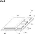
- FIG. 2 is a perspective view of the circuit substrate 200 according to one embodiment.
- the circuit substrate 200 includes the ceramic plate 10 and a plurality of conductor portions 20A provided on one main surface 10A of the ceramic plate 10.
- the shapes of the plurality of conductor portions 20A may all be the same, or may include different shapes as illustrated in FIG. 2 .
- the conductor portion 20A includes the metal layer 21 and the thermal sprayed layer 22 in this order from the ceramic plate 10 side. That is, the conductor portion 20A has a laminated structure similar to the laminated portion 20 of FIG. 1 .
- the circuit substrate 200 also includes a plurality of conductor portions 20A on the other main surface of the ceramic plate 10. In a modification, the circuit 200 may include one or more conductor portions 20A on only one main surface.
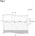
- FIG. 3 is an enlarged cross-sectional view illustrating a part of a cross-section along the stacking direction of the metal layer 21 and the thermal sprayed layer 22 of the composite substrate 100 (the circuit substrate 200) in an enlarged manner.
- FIG. 3 illustrates a part of one metal layer 21 and the ceramic plate 10 and the thermal sprayed layer 22 adjacent to the metal layer 21 in the composite substrate 100 (the circuit substrate 200).
- An intermetallic compound 30 is scattered along a boundary line L between the thermal sprayed layer 22 and the metal layer 21.
- the intermetallic compound 30 contains copper and aluminum as constituent elements.
- the intermetallic compound 30 contains at least one selected from the group consisting of Cu 9 Al 4 , CuAl, and CuAl 2 .
- the intermetallic compound 30 can be identified by X-ray diffraction.
- the intermetallic compound 30 is scattered between the metal layer 21 and the thermal sprayed layer 22.
- the intermetallic compound 30 in the intervening portion 42 contains copper and aluminum as constituent elements, the intermetallic compound 30 is compatible with both the metal layer 21 and the thermal sprayed layer 22, and has a function of firmly bonding the metal layer 21 and the thermal sprayed layer 22. Accordingly, the electrical conductivity between the metal layer 21 and the thermal sprayed layer 22 can be improved. In addition, since the contact portion 40 bears the strain caused by thermal stress due to heat cycles, the concentration of the thermal stress on the intermetallic compound 30 in the intervening portion 42 can be reduced. In this way, cracking of the intermetallic compound, which is usually hard and brittle, can be reduced, and durability against heat cycles can be improved.
- the length of the intermetallic compound 30 (the intervening portion 42) is less than 25 ⁇ m along the boundary line L on the metal layer 21 side of the thermal sprayed layer 22 when viewed in a cross-section as illustrated in FIG. 3 .
- the length of the intermetallic compound 30 along the boundary line L can be measured by the following procedure.
- the composite substrate is cut using a diamond cutter, a band saw, or the like, and polished with diamond abrasive grains or the like to obtain a cross-section as illustrated in FIG. 3 .
- the cross-section is observed with a scanning electron microscope (SEM), and a photograph of a magnified image of 3000 times is taken.
- SEM scanning electron microscope
- the outer edge on the metal layer 21 side of the thermal sprayed layer 22 shown in the photograph is taken as the boundary line L, and the length of the intermetallic compound 30 along the boundary line L is measured.
- the length can be calculated by, for example, disposing a string along the boundary line L and calculating the length of the string at the intermetallic compound 30 portion and the magnification of the photograph.
- the measurement is performed by using photographs taken in five different regions which are randomly selected in the cross-section.
- an intermetallic compound whose length measured in this manner is 25 ⁇ m or more is considered to be layered.
- the intermetallic compound is scattered means that the maximum value of the length of the intermetallic compound 30 along the boundary line L is less than 25 ⁇ m in the SEM photographs taken in the above-described five regions. In other words, in the SEM photographs taken in the above-described five regions, only intermetallic compounds 30 having the length along the boundary line L of less than 25 ⁇ m are included. In the SEM photographs taken in the above-described five regions, the length of the intermetallic compound 30 along the boundary line L may be 20 ⁇ m or less, and may be 15 ⁇ m or less, from the viewpoint of further improving durability against heat cycles. Accordingly, concentration of stress on the intermetallic compound 30 is further reduced, and durability against heat cycles can be sufficiently increased. The length of the intermetallic compound 30 along the boundary line L may be 2 ⁇ m or more, and may be 5 ⁇ m or more from the viewpoint of forming the thermal sprayed layer 22 in which work hardening is sufficiently alleviated.
- the coverage of the thermal sprayed layer 22 by the intermetallic compound based on the length of the boundary line L of the thermal sprayed layer 22 on the metal layer 21 side may be 75% or less, and may be less than 50%. Accordingly, a ratio of the contact portion 40 in which the thermal sprayed layer 22 and the metal layer 21 are in direct contact with each other on the boundary line L increases, and thus it is possible to further reduce concentration of thermal stress on the intermetallic compound 30 during heat cycles. Therefore, durability against heat cycles can be sufficiently improved.
- the coverage may be 10% or more, or may be 30% or more, from the viewpoint of sufficiently alleviating work hardening of the thermal sprayed layer 22 and from the viewpoint of more firmly bonding the metal layer 21 and the thermal sprayed layer 22.
- the coverage can be measured by using the photograph of the image enlarged by 3000 times and the string. That is, for example, the string is disposed along the boundary line L, and the length (L0) of the entire boundary line L and the length (L1) of the strings in the portion of the intermetallic compound 30 (the intervening portion 42) shown in the photograph are measured.
- the length (L1) is the sum of the lengths along the boundary line L of the respective intermetallic compounds 30.
- the measurement is performed by using photographs taken in five regions randomly selected on the cross-section. A calculation of (L1/L0) ⁇ 100 is performed using each photograph, and the mean value of the calculated values is taken as the coverage in the present disclosure.
- An example of a method of manufacturing the composite substrate 100 includes:
- both the metal layer 21 and the thermal sprayed layer 22 are formed by thermal spraying.
- a powder spray device can be used to form these layers.
- the first metallic particles are thermal sprayed onto the main surface of the ceramic plate 10 using the powder spray device.
- the first precursor film is formed on the main surface of the ceramic plate 10.
- the first precursor film may be formed on one main surface and then the first precursor film may be formed on the other main surface.
- the composite substrate having the laminated portion 20 on only one main surface of the ceramic plate 10 is manufactured, the first precursor film may be formed on only one main surface.
- the first metallic particles may be aluminum particles or aluminum alloy particles containing other metal elements, such as aluminum-magnesium alloy particles and aluminum-lithium alloy particles.
- aluminum alloy particles containing a metal element having a higher oxygen affinity than aluminum, such as magnesium and lithium are used, the metal element such as magnesium or lithium reacts with an oxide on the surface of the ceramic plate during heating after film formation, and these tend to be strongly bonded.
- the content of metal elements such as magnesium and lithium in the first metallic particle may be 6.0% by mass or less with respect to the entire first metallic particle.
- the first precursor film formed on the ceramic plate is heated in the inert gas atmosphere to form the metal layer 21.
- the heating temperature at this time may be 400 to 600°C.
- the reaction between aluminum and the oxide on the surface of the ceramic plate 10 sufficiently proceeds. Accordingly, the metal layer 21 and the ceramic plate 10 can be strongly bonded to each other.
- By heating the first precursor film at a temperature of 600°C or lower it is possible to reduce the influence of softening of the first precursor film.
- the metal layer 21 is formed by thermal spraying, but the forming process is not limited thereto.
- the metal layer 21 may be provided on the ceramic plate 10 by preparing a metal plate containing at least one selected from the group consisting of aluminum and an aluminum alloy, and bonding the metal plate using a brazing material. In this case, it may be necessary to etch the metal layer 21 in order to form a conductor portion having a predetermined pattern on the ceramic plate 10.
- the metal layer 21 having a pattern may be formed on the ceramic plate 10 by disposing a mask material covering part of the main surface of the ceramic plate 10.
- the conductor portion having high shape accuracy can be easily formed without performing an additional process such as etching after film formation.
- the thermal sprayed layer 22 is formed on the main surface of the metal layer 21 by thermal spraying.
- the thermal sprayed layer 22 is formed by, for example, the following procedure.
- the second metallic particles are thermal sprayed onto the main surface of the metal layer 21 opposite to the ceramic plate 10 to form the second precursor film.
- the second metallic particles include copper particles, copper-phosphorus alloy particles, and copper-molybdenum alloy particles.
- the content of the metal element other than copper in the second metallic particle may be 6.0% by mass or less with respect to the entire second metallic particle.
- the thermal sprayed layer 22 is formed by heating the second precursor film formed on the main surface of the metal layer 21 in the inert gas atmosphere.
- the heating temperature of the second precursor film at this time may be 250 to 300°C, and may be 250 to 290°C. If the heat treatment temperature is too high, the intermetallic compound 30 is likely to be formed in a layered form, and the durability against heat cycles tends to decrease. On the other hand, if the heat treatment temperature is too low, work hardening in the thermal sprayed layer 22 cannot be sufficiently alleviated, and excellent electrical conductivity tends to be impaired. In addition, the amount of the intermetallic compound 30 produced tends to decrease.
- the heating time of the second precursor film at the above heating temperature may be 5 minutes to 1 hour.
- the heating time is too short, work hardening of the thermal sprayed layer 22 cannot be sufficiently alleviated, and excellent electrical conductivity tends to be impaired.
- the amount of the intermetallic compound 30 produced tends to decrease.
- the heating time is too long, the intermetallic compound 30 is likely to be formed in a layered form, and the durability against heat cycles tends to decrease.
- the thermal sprayed layer 22 having the same pattern (the circuit pattern) as the metal layer 21 can be formed by using similar mask material as that used when the first precursor is deposited. With this method, the conductor portion having high shape accuracy can be easily formed without performing an additional process such as etching after film formation. In this manner, the circuit substrate having the conductor portion on the ceramic plate 10 may be manufactured.
- the thermal sprayed layer 22 may be formed so as to be slightly smaller than the metal layer 21.
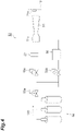
- FIG. 4 is a diagram illustrating an example of a powder spray device used for forming the first precursor film and the second precursor film.
- a powder spray device 50 includes a gas supply unit 54, a heater 56, a particle supply unit 57, a nozzle 51 of a spray gun having a tapered divergent shape, and a pipe connecting the gas supply unit 54, the heater 56, the particle supply unit 57, and the nozzle 51.
- a first pressure regulation unit 55a is provided downstream of the gas supply unit 54. The pipe branches into two parts on the downstream side of the first pressure regulation unit 55a.
- the second pressure regulation unit 55b and the heater 56 are connected in this order to one of the two branched pipes, and the third pressure regulation unit 55c and the particle supply unit 57 are connected in this order to the other of the two branched pipes.
- the heater 56 and the particle supply unit 57 are connected to the nozzle 51 via pipes.
- the gas supply unit 54 supplies an inert gas which functions as a working gas.
- the inert gas may be, for example, helium gas, nitrogen gas, or a mixed gas thereof.
- a part of the working gas supplied from the gas supply unit 54 is pressure-regulated by the second pressure regulation unit 55b, and then heated by the heater 56 as necessary.
- the heating temperature may be, for example, 10 to 270°C when forming the first precursor film.
- the heating temperature may be, for example, 10 to 650°C when forming the second precursor film.
- the heated working gas is supplied to the nozzle 51 of the spray gun.
- the other part of the working gas supplied from the gas supply unit 54 is pressure-regulated by the third pressure regulation unit 55c and then supplied to the particle supply unit 57.
- Metallic particles for film formation are supplied from the particle supply unit 57 to the nozzle 51 of the spray gun together with working gas.
- the gauge pressure of the working gas in the inlet 51a of the nozzle 51 may be 1.5 to 5.0 MPa.
- the heating temperature by the heater 56 is usually set lower than the melting point or softening point of the metallic particles to be deposited.
- the first metallic particles or the second metallic particles and the working gas supplied to the nozzle 51 of the spray gun are compressed by passing through the tapered portion, and are accelerated by expanding at once in the divergent portion on the downstream side thereof.
- the metallic particles are heated to a predetermined temperature, accelerated to a predetermined speed, and then ejected from the outlet of the nozzle 51.
- the first metallic particles or the second metallic particles ejected from the nozzle 51 are sprayed to the main surface of the ceramic plate 10.
- the first metallic particles and the second metallic particles are deposited, while colliding in a solid phase state, on the main surface of the ceramic plate 10 and the surface of the metal layer 21, respectively, thereby forming the first precursor film and the second precursor film.
- a first precursor film 21a formed on the main surface of the ceramic plate 10 is illustrated.
- the composite substrate 100 which has the ceramic plate 10 and the laminated portion 20 including the metal layer 21 and the thermal sprayed layer 22 in this order from the ceramic plate 10 side on both main surfaces of the ceramic plate 10, and in which the intermetallic compound 30 containing copper and aluminum as constituent elements is scattered between the metal layer 21 and the thermal sprayed layer 22.
- the description of the composite substrate 100 may also be applied to a method of manufacturing the composite substrate 100.
- An example of a method of manufacturing a circuit substrate may include patterning the laminated portion 20 of the composite substrate 100 obtained by the above-described manufacturing method by etching to form a conductor portion.
- the conductor portion may be formed on both main surfaces of the ceramic plate 10 without performing etching by using a mask material when depositing the first precursor film and the second precursor film.
- the first precursor film and the second precursor film each having a predetermined pattern shape may be formed using the mask material in each of the steps of forming the first precursor film and the second precursor film in the manufacturing method of the composite substrate described above. Otherwise, it can be produced in the same way as the composite substrate.
- the second precursor film is heated so that the intermetallic compound 30 containing copper and aluminum as constituent elements is scattered. Accordingly, it is possible to obtain the thermal sprayed layer 22 in which work hardening is alleviated.
- the thermal sprayed layer 22 has excellent electrical conductivity.
- the intermetallic compound 30 is not formed in a layered manner but is formed in a scattered manner, it is possible to reduce occurrence of cracks due to heat cycles and to improve durability against heat cycles. Therefore, the power module having the composite substrate 100 and the circuit substrate 200 is excellent in reliability.
- the intermetallic compound 30 being scattered between the metal layer 21 and thermal sprayed layer 22 may strengthen the bonding between the metal layer 21 and the thermal sprayed layer 22, thereby improving electrical conductivity.
- the present disclosure is not limited to the above-described embodiments.
- the laminated portion 20 (the conductor portions 20A) may be provided on only one main surface of the ceramic plate 10.
- at least one of thicknesses, shapes, and compositions of the metal layer 21 and the thermal sprayed layer 22 in the pair of laminated portions 20 (the conductor portion 20A) interposing the ceramic plate 10 therebetween may be different from each other.
- a part of the main surface of the substrate was masked with an iron mask material.
- Aluminum particles gas-atomized powder manufactured by Kojundo Chemical Laboratory Co., Ltd., median diameter: 24 ⁇ m
- the aluminum film was formed under the following conditions: nitrogen gas was used as a working gas; the temperature of the working gas was 20°C; and the pressure of the working gas at the nozzle inlet of the spray gun was 1.5 MPa.
- the formed aluminum film was heat-treated at 500°C for 3 hours in a nitrogen atmosphere to obtain a metal layer made of aluminum having a thickness of 0.2mm.
- Copper particles water atomized powder manufactured by Fukuda Metal Foil & Powder Co., Ltd., median diameter: 17 ⁇ m
- the copper film was formed under the following conditions: nitrogen gas was used as a working gas: the temperature of the working gas was set to 350°C, and the pressure of the working gas at the nozzle inlet of the spray gun was set to 3 MPa.
- the copper film was heat-treated at 280°C for 10 minutes in a nitrogen atmosphere to obtain a thermal sprayed layer made of copper having a thickness of 0.4 mm.
- the thermal sprayed layer was formed to have vertical and horizontal lengths smaller than those of the metal layer by about 50 ⁇ m.
- the metal layer and the thermal sprayed layer were sequentially formed on both main surfaces of the ceramic plate in the above-described procedure, and the circuit substrate of Example 1 including the conductor portion having the metal layer and the thermal sprayed layer from the ceramic plate side on both main surfaces of the ceramic plate was obtained.
- FIG. 5 is an SEM photograph showing a cross-section of the circuit substrate of Example 1.
- the electrical conductivity of the conductor portion was measured by the eddy current method.
- the measurement was performed using a digital conductivity meter (manufactured by GE Sensing & Inspection Technologies Co., Ltd., trade name: AutoSigma3000). The results are shown in Table 1.
- Vickers hardness on the surface of the thermal sprayed layer was measured. The measurement was performed using a dynamic ultra-micro hardness tester (manufactured by Shimadzu Corporation, trade name: DUH211). The results are shown in Table 1.
- Circuit substrates were manufactured in the same manner as in Example 1 except that the heating temperature and the heating time of the copper film in a nitrogen atmosphere were changed as shown in Table 1, and each evaluation was performed. The results of each evaluation are shown in Table 1.
- a circuit substrate was manufactured in the same manner as in Example 1 except that the heat treatment of the copper film was not performed, and each evaluation was performed. The results of each evaluation are shown in Table 1.
- FIG. 6 is an SEM photograph showing a cross-section of the circuit substrate of Example 3.
- FIG. 7 is an SEM photograph showing a cross-section of the circuit substrate of Comparative Example 1.
- FIG. 8 is an SEM photograph showing a cross-section of the circuit substrate of Comparative Example 2.
- FIG. 9 is an SEM photograph showing a cross-section of the circuit substrate of Comparative Example 3.
- FIG. 10 is an SEM photograph showing a cross-section of the circuit substrate of Comparative Example 4. In the circuit substrate of each example, it was confirmed that the intermetallic compound 30 was scattered between the thermal sprayed layer 22 and the metal layer 21.
- the conductor portion of the circuit substrate of each example had excellent electrical conductivity. Further, from the results of the Vickers hardness, it was confirmed that the work hardening of the thermal sprayed layer was sufficiently alleviated in each Example. On the other hand, it was confirmed that Comparative Examples 1 to 3, in which the intermetallic compound was formed in a layered manner, were inferior to Examples 1 to 3 in terms of heat cycle durability. The circuit substrate of Comparative Example 4 in which the intermetallic compound was not scattered between the metal layer and the thermal sprayed layer had low electrical conductivity.
- 10 ceramic plate, 10A: main surface, 20: laminated portion, 20A: conductor portion, 21: metal layer, 21a: first precursor film, 22: thermal sprayed layer, 30: intermetallic compound, 40: contact portion, 42: intervening portion, 50: powder spray device, 51: nozzle, 51a: inlet, 54: gas supply unit, 55a: first pressure regulation unit, 55b: second pressure regulation unit, 55c: third pressure regulation unit, 56: heater, 57: particle supply unit, 100: composite substrate, 200: circuit substrate.
Landscapes
- Chemical & Material Sciences (AREA)
- Engineering & Computer Science (AREA)
- Materials Engineering (AREA)
- Organic Chemistry (AREA)
- Chemical Kinetics & Catalysis (AREA)
- Mechanical Engineering (AREA)
- Metallurgy (AREA)
- Physics & Mathematics (AREA)
- Plasma & Fusion (AREA)
- Ceramic Engineering (AREA)
- Inorganic Chemistry (AREA)
- Microelectronics & Electronic Packaging (AREA)
- Structural Engineering (AREA)
- Coating By Spraying Or Casting (AREA)
- Laminated Bodies (AREA)
- Parts Printed On Printed Circuit Boards (AREA)
- Other Surface Treatments For Metallic Materials (AREA)
Abstract
Description
- The present disclosure relates to a composite substrate and a method for manufacturing the same, and a circuit substrate and a method for manufacturing the same.
- In recent years, power modules for high-power control have been used in industrial equipment such as motors and products such as electric vehicles. In such a power module, a circuit substrate including a ceramic plate having high thermal conductivity is used in order to efficiently diffuse heat generated from semiconductor elements.
- Copper is mainly used for a metal circuit portion of the circuit substrate because a high voltage and a high current may flow. However, since the ceramic plate is repeatedly subjected to thermal shocks due to environmental changes during use, heat due to switching, and the like, the copper circuit may peel off from the ceramic plate due to thermal stress caused by a difference in thermal expansion coefficient between copper and ceramic. Therefore, a technique is known in which an aluminum layer that is easily plastically deformed is provided between the ceramic plate and the copper circuit to alleviate the thermal stress. Under such circumstances, Patent Document 1 proposes a technique in which an intermetallic compound layer and a eutectic layer are formed in a bonding layer between an aluminum member and a copper member to reduce occurrence of cracks in the bonding layer.
- [Patent Document 1]
Japanese Unexamined Patent Publication No. 2019-87608 - Intermetallic compounds have properties of being hard and brittle. Therefore, when an intermetallic compound is formed in a layer shape, there is a concern that the intermetallic compound may cause occurrence of cracks under a heat cycle condition in which heating and cooling are repeated.
- Accordingly, the present disclosure provides a composite substrate and a circuit substrate that have excellent durability against heat cycles and high electrical conductivity. In addition, the present disclosure provides a composite substrate and a method for manufacturing a circuit substrate capable of manufacturing the composite substrate and the circuit substrate having excellent durability against heat cycles and high electrical conductivity.
- A composite substrate according to an aspect of the present disclosure includes, in this order: a ceramic plate; a metal layer containing at least one selected from the group consisting of aluminum and an aluminum alloy; and a thermal sprayed layer containing at least one selected from the group consisting of copper and a copper alloy, in which an intermetallic compound containing copper and aluminum as constituent elements is scattered between the metal layer and the thermal sprayed layer.
- In the composite substrate, since the intermetallic compound containing copper and aluminum as constituent elements is scattered between the metal layer and the thermal sprayed layer, the metal layer and the thermal sprayed layer are strongly bonded to each other and the composite substrate has high electrical conductivity. In addition, since the intermetallic compound is not formed in a layered form but scattered, it is possible to reduce occurrence of cracks due to heat cycles and improve durability against heat cycles.
- The composite substrate may include, between the metal layer and the thermal sprayed layer, a contact portion in which the metal layer and the thermal sprayed layer are in direct contact with each other, and an intervening portion in which the intermetallic compound is interposed, when viewed from a cross-section cut along the stacking direction of the metal layer and the thermal sprayed layer. Accordingly, both the bonding strength between the metal layer and the thermal sprayed layer and durability against heat cycles can be achieved at a higher level.
- The intermetallic compound may contain at least one selected from the group consisting of Cu9Al4, CuAl, and CuAl2. Accordingly, both the bonding strength between the metal layer and the thermal sprayed layer and the durability against heat cycles can be achieved at a higher level.
- A length of the intermetallic compound along a boundary line on the metal layer side of the thermal sprayed layer may be 15 µm or less when viewed from a cross-section cut along a stacking direction of the metal layer and the thermal sprayed layer. When the cross-section is viewed, the coverage of the thermal sprayed layer by the intermetallic compound may be 75% or less with respect to the length of the boundary line on the metal layer side of the thermal sprayed layer. Such a composite substrate can have sufficiently high durability against heat cycles.
- A circuit substrate according to an aspect of the present disclosure includes a ceramic plate and a conductor portion on the ceramic plate, in which the conductor portion includes a metal layer containing in this order from the ceramic plate side at least one selected from the group consisting of aluminum and an aluminum alloy and a thermal sprayed layer containing at least one selected from the group consisting of copper and a copper alloy, and an intermetallic compound containing copper and aluminum as constituent elements is scattered between the metal layer and the thermal sprayed layer.
- In the conductor portion of the circuit substrate, since the intermetallic compound having copper and aluminum as constituent elements is scattered between the metal layer and the thermal sprayed layer, the metal layer and the thermal sprayed layer are strongly bonded to each other, and thus the conductor portion has high electrical conductivity. In addition, since the intermetallic compound is not formed in a layered form but scattered, it is possible to reduce occurrence of cracks due to heat cycles and improve durability against heat cycles.
- A method of manufacturing a composite substrate according to an aspect of the present disclosure includes: forming a precursor film by spraying metallic particles containing at least one selected from the group consisting of copper and a copper alloy on a surface of a metal layer provided on a ceramic plate and containing at least one selected from the group consisting of aluminum and an aluminum alloy; and heating the precursor film to obtain a thermal sprayed layer and to generate an intermetallic compound so as to be scattered between the metal layer and the thermal sprayed layer.
- In the method of manufacturing the composite substrate, the precursor film is heated to generate the intermetallic compound including copper and aluminum as constituent elements so as to be scattered between the metal layer and the thermal sprayed layer. Since the precursor film is heated until the intermetallic compound is generated so as to be scattered, a thermal sprayed layer in which work hardening is sufficiently alleviated can be obtained. The thermal sprayed layer in which the work hardening is alleviated as described above has high electrical conductivity. In addition, since the intermetallic compound is not formed in a layered form but is scattered, it is possible to reduce occurrence of cracks due to heat cycles and to improve durability against heat cycles.
- A method of manufacturing a circuit substrate according to an aspect of the present disclosure includes: forming a precursor film by spraying metallic particles containing at least one selected from the group consisting of copper and a copper alloy on a surface of a metal layer provided on a ceramic plate and containing at least one selected from the group consisting of aluminum and an aluminum alloy; and heating the precursor film to obtain a thermal sprayed layer and to generate an intermetallic compound so as to be scattered between the metal layer and the thermal sprayed layer, thereby forming a conductor portion having a predetermined pattern on the ceramic plate.
- In the method of manufacturing the circuit substrate, the conductor portion is formed by heating the precursor film to generate the intermetallic compound containing copper and aluminum as constituent elements in a scattered manner between the metal layer and the thermal sprayed layer. Since the precursor film is heated until the intermetallic compound is generated so as to be scattered, a thermal sprayed layer in which work hardening is sufficiently alleviated can be obtained. The thermal sprayed layer in which the work hardening is alleviated as described above has high electrical conductivity. In addition, since the intermetallic compound is not formed in a layered form but scattered, it is possible to reduce the occurrence of cracks due to heat cycles and improve durability against heat cycles.
- According to the present disclosure, it is possible to provide a composite substrate and a circuit substrate having excellent durability against heat cycles and high electrical conductivity. In addition, according to the present disclosure, it is possible to provide a method for manufacturing a composite substrate and a circuit substrate capable of manufacturing the composite substrate and the circuit substrate having excellent durability against heat cycles and high electrical conductivity.
-
-
FIG. 1 is a cross-sectional view illustrating a composite substrate according to an embodiment. -
FIG. 2 is a plan view illustrating a circuit substrate according to an embodiment. -
FIG. 3 is an enlarged cross-sectional view illustrating a portion of a cross-section of the composite substrate (the circuit substrate) according to an embodiment in an enlarged manner. -
FIG. 4 is a diagram illustrating an example of a powder spray device used for forming a first precursor film and a second precursor film. -
FIG. 5 is a scanning electron microscope photograph showing a cross-section of a circuit substrate of Example 1. -
FIG. 6 is a scanning electron microscope photograph showing a cross-section of a circuit substrate of Example 3. -
FIG. 7 is a scanning electron microscope photograph showing a cross-section of a circuit substrate of Comparative Example 1. -
FIG. 8 is a scanning electron microscope photograph showing a cross-section of a circuit substrate of Comparative Example 2. -
FIG. 9 is a scanning electron microscope photograph showing a cross-section of a circuit substrate of Comparative Example 3. -
FIG. 10 is a scanning electron microscope photograph showing a cross-section of a circuit substrate of Comparative Example 4. - Hereinafter, an embodiment of the present disclosure will be described with reference to the drawings in some cases. However, the following embodiments are examples for describing the present disclosure, and are not intended to limit the present disclosure to the following contents. In the description, the same elements or elements having the same functions are denoted by the same reference numerals, and redundant description will be omitted in some cases. The positional relationship such as up, down, left, and right is based on the positional relationship shown in the drawings unless otherwise specified. Further, the dimensional ratios of the elements are not limited to the ratios shown in the drawings.
-
FIG. 1 is a cross-sectional view taken along a stacking direction of a metal layer and a thermal sprayed layer of acomposite substrate 100 according to an embodiment. Thecomposite substrate 100 illustrated inFIG. 1 includes aceramic plate 10 and a pair of laminatedportions 20 sandwiching theceramic plate 10. The laminatedportion 20 includes, in this order from theceramic plate 10 side, ametal layer 21 containing at least one selected from the group consisting of aluminum and an aluminum alloy, and a thermal sprayedlayer 22 containing at least one selected from the group consisting of copper and a copper alloy.FIG. 1 illustrates a cross-section along the stacking direction of themetal layer 21 and the thermal sprayedlayer 22. - One or both of the laminated
portions 20 may be a conductor portion (a metal circuit) having a predetermined pattern. In this case, thecomposite substrate 100 is a circuit substrate. A semiconductor element is bonded to the conductor portion via, for example, a silver bonding layer to form a circuit. - The
ceramic plate 10 may be made of an ordinary ceramic. Examples of the ceramics include aluminum nitride (AlN), silicon nitride (Si3N4), and aluminum oxide (Al2O3). The thickness of theceramic plate 10 may be, for example, 0.2 to 1.0 mm from the viewpoint of improving durability against heat cycles and thinning while maintaining excellent insulation properties. - The
metal layer 21 has a function of reducing thermal stress generated during heat cycles due to a difference in thermal expansion coefficient between theceramic plate 10 and the thermal sprayedlayer 22 while maintaining high thermal conductivity of thecomposite substrate 100. In order to sufficiently exhibit such a function, themetal layer 21 may contain at least one selected from the group consisting of aluminum and an aluminum alloy as a main component. Examples of the aluminum alloy include an aluminum-magnesium alloy and an aluminum-lithium alloy. Here, the "main component" is a component having a content of 90% by mass or more with respect to theentire metal layer 21. The thickness of themetal layer 21 may be, for example, 0.05 to 1 mm from the viewpoint of achieving thinning while sufficiently reducing thermal stresses generated during heat cycles. - The
metal layer 21 may be formed by applying a brazing material on a main surface of theceramic plate 10 and bonding a metal plate, or may be a thermal sprayed layer formed by thermally spraying metallic particles on the main surface of theceramic plate 10 and performing a heat treatment. In the case of the thermal sprayed layer, themetal layer 21 may be formed on the main surface of theceramic plate 10 without using the brazing material. If a mask is used at the time of thermal spraying, a conductor portion having a predetermined pattern can be formed without etching. - The thermal sprayed
layer 22 may contain at least one selected from the group consisting of copper and a copper alloy as a main component from the viewpoint of sufficiently increasing the electrical conductivity while maintaining high thermal conductivity of thecomposite substrate 100. Examples of the copper alloy include a copper-phosphorus alloy and a copper-molybdenum alloy. Here, the "main component" is a component having a content of 90% by mass or more with respect to the entire thermal sprayedlayer 22. The thickness of the thermal sprayedlayer 22 may be, for example, 0.1 to 3 mm from the viewpoint of improving durability against heat cycles and thinning while sufficiently increasing electrical conductivity and thermal conductivity. - The thermal sprayed
layer 22 is formed by thermally spraying metallic particles on the main surface of theceramic plate 10 and heat-treating the thermal sprayed particles. The thermal sprayedlayer 22 can be formed on the main surface of themetal layer 21 without using a brazing material. If a mask material is used at the time of thermal spraying, a conductor portion having a predetermined pattern can be formed without etching. -
FIG. 2 is a perspective view of thecircuit substrate 200 according to one embodiment. Thecircuit substrate 200 includes theceramic plate 10 and a plurality ofconductor portions 20A provided on onemain surface 10A of theceramic plate 10. The shapes of the plurality ofconductor portions 20A may all be the same, or may include different shapes as illustrated inFIG. 2 . Theconductor portion 20A includes themetal layer 21 and the thermal sprayedlayer 22 in this order from theceramic plate 10 side. That is, theconductor portion 20A has a laminated structure similar to thelaminated portion 20 ofFIG. 1 . Thecircuit substrate 200 also includes a plurality ofconductor portions 20A on the other main surface of theceramic plate 10. In a modification, thecircuit 200 may include one ormore conductor portions 20A on only one main surface. -
FIG. 3 is an enlarged cross-sectional view illustrating a part of a cross-section along the stacking direction of themetal layer 21 and the thermal sprayedlayer 22 of the composite substrate 100 (the circuit substrate 200) in an enlarged manner.FIG. 3 illustrates a part of onemetal layer 21 and theceramic plate 10 and the thermal sprayedlayer 22 adjacent to themetal layer 21 in the composite substrate 100 (the circuit substrate 200). Anintermetallic compound 30 is scattered along a boundary line L between the thermal sprayedlayer 22 and themetal layer 21. Theintermetallic compound 30 contains copper and aluminum as constituent elements. For example, theintermetallic compound 30 contains at least one selected from the group consisting of Cu9Al4, CuAl, and CuAl2. Theintermetallic compound 30 can be identified by X-ray diffraction. - In the composite substrate 100 (the circuit substrate 200), the
intermetallic compound 30 is scattered between themetal layer 21 and the thermal sprayedlayer 22. Acontact portion 40 where themetal layer 21 and the thermal sprayedlayer 22 are in direct contact with each other and an interveningportion 42 where theintermetallic compound 30 is interposed between themetal layer 21 and the thermal sprayedlayer 22 are formed between themetal layer 21 and the thermal sprayedlayer 22. - Since the
intermetallic compound 30 in the interveningportion 42 contains copper and aluminum as constituent elements, theintermetallic compound 30 is compatible with both themetal layer 21 and the thermal sprayedlayer 22, and has a function of firmly bonding themetal layer 21 and the thermal sprayedlayer 22. Accordingly, the electrical conductivity between themetal layer 21 and the thermal sprayedlayer 22 can be improved. In addition, since thecontact portion 40 bears the strain caused by thermal stress due to heat cycles, the concentration of the thermal stress on theintermetallic compound 30 in the interveningportion 42 can be reduced. In this way, cracking of the intermetallic compound, which is usually hard and brittle, can be reduced, and durability against heat cycles can be improved. - The length of the intermetallic compound 30 (the intervening portion 42) is less than 25 µm along the boundary line L on the
metal layer 21 side of the thermal sprayedlayer 22 when viewed in a cross-section as illustrated inFIG. 3 . The length of theintermetallic compound 30 along the boundary line L can be measured by the following procedure. The composite substrate is cut using a diamond cutter, a band saw, or the like, and polished with diamond abrasive grains or the like to obtain a cross-section as illustrated inFIG. 3 . The cross-section is observed with a scanning electron microscope (SEM), and a photograph of a magnified image of 3000 times is taken. The outer edge on themetal layer 21 side of the thermal sprayedlayer 22 shown in the photograph is taken as the boundary line L, and the length of theintermetallic compound 30 along the boundary line L is measured. The length can be calculated by, for example, disposing a string along the boundary line L and calculating the length of the string at theintermetallic compound 30 portion and the magnification of the photograph. The measurement is performed by using photographs taken in five different regions which are randomly selected in the cross-section. In the present disclosure, an intermetallic compound whose length measured in this manner is 25 µm or more is considered to be layered. - In the present disclosure, "the intermetallic compound is scattered" means that the maximum value of the length of the
intermetallic compound 30 along the boundary line L is less than 25 µm in the SEM photographs taken in the above-described five regions. In other words, in the SEM photographs taken in the above-described five regions, onlyintermetallic compounds 30 having the length along the boundary line L of less than 25 µm are included. In the SEM photographs taken in the above-described five regions, the length of theintermetallic compound 30 along the boundary line L may be 20 µm or less, and may be 15 µm or less, from the viewpoint of further improving durability against heat cycles. Accordingly, concentration of stress on theintermetallic compound 30 is further reduced, and durability against heat cycles can be sufficiently increased. The length of theintermetallic compound 30 along the boundary line L may be 2 µm or more, and may be 5 µm or more from the viewpoint of forming the thermal sprayedlayer 22 in which work hardening is sufficiently alleviated. - When the cross-section is viewed, the coverage of the thermal sprayed
layer 22 by the intermetallic compound based on the length of the boundary line L of the thermal sprayedlayer 22 on themetal layer 21 side may be 75% or less, and may be less than 50%. Accordingly, a ratio of thecontact portion 40 in which the thermal sprayedlayer 22 and themetal layer 21 are in direct contact with each other on the boundary line L increases, and thus it is possible to further reduce concentration of thermal stress on theintermetallic compound 30 during heat cycles. Therefore, durability against heat cycles can be sufficiently improved. The coverage may be 10% or more, or may be 30% or more, from the viewpoint of sufficiently alleviating work hardening of the thermal sprayedlayer 22 and from the viewpoint of more firmly bonding themetal layer 21 and the thermal sprayedlayer 22. - Similar to the measurement of the length of the
intermetallic compound 30, the coverage can be measured by using the photograph of the image enlarged by 3000 times and the string. That is, for example, the string is disposed along the boundary line L, and the length (L0) of the entire boundary line L and the length (L1) of the strings in the portion of the intermetallic compound 30 (the intervening portion 42) shown in the photograph are measured. When there are a plurality ofintermetallic compounds 30, the length (L1) is the sum of the lengths along the boundary line L of the respective intermetallic compounds 30. The measurement is performed by using photographs taken in five regions randomly selected on the cross-section. A calculation of (L1/L0) × 100 is performed using each photograph, and the mean value of the calculated values is taken as the coverage in the present disclosure. - An example of a method of manufacturing the
composite substrate 100 includes: - a step of forming a first precursor film by spraying first metallic particles containing at least one selected from the group consisting of aluminum and an aluminum alloy onto the main surface of the
ceramic plate 10 together with an inert gas; - a step of forming the
metal layer 21 by heating the first precursor film in the inert gas atmosphere; - a step of forming a second precursor film by spraying second metallic particles containing at least one selected from the group consisting of copper and a copper alloy onto the surface of the
metal layer 21 provided on theceramic plate 10; and - a heating step of heating the second precursor film to obtain the thermal sprayed
layer 22 and to generate theintermetallic compound 30 so as to be scattered between themetal layer 21 and the thermal sprayedlayer 22. - In this example, both the
metal layer 21 and the thermal sprayedlayer 22 are formed by thermal spraying. A powder spray device can be used to form these layers. Specifically, the first metallic particles are thermal sprayed onto the main surface of theceramic plate 10 using the powder spray device. Accordingly, the first precursor film is formed on the main surface of theceramic plate 10. In this case, the first precursor film may be formed on one main surface and then the first precursor film may be formed on the other main surface. When the composite substrate having thelaminated portion 20 on only one main surface of theceramic plate 10 is manufactured, the first precursor film may be formed on only one main surface. - The first metallic particles may be aluminum particles or aluminum alloy particles containing other metal elements, such as aluminum-magnesium alloy particles and aluminum-lithium alloy particles. When aluminum alloy particles containing a metal element having a higher oxygen affinity than aluminum, such as magnesium and lithium, are used, the metal element such as magnesium or lithium reacts with an oxide on the surface of the ceramic plate during heating after film formation, and these tend to be strongly bonded. From the viewpoint of further improving the durability against heat cycles, the content of metal elements such as magnesium and lithium in the first metallic particle may be 6.0% by mass or less with respect to the entire first metallic particle.
- The first precursor film formed on the ceramic plate is heated in the inert gas atmosphere to form the
metal layer 21. The heating temperature at this time may be 400 to 600°C. By heating the first precursor film at a temperature of 400°C or higher, the reaction between aluminum and the oxide on the surface of theceramic plate 10 sufficiently proceeds. Accordingly, themetal layer 21 and theceramic plate 10 can be strongly bonded to each other. By heating the first precursor film at a temperature of 600°C or lower, it is possible to reduce the influence of softening of the first precursor film. - In this example, the
metal layer 21 is formed by thermal spraying, but the forming process is not limited thereto. For example, themetal layer 21 may be provided on theceramic plate 10 by preparing a metal plate containing at least one selected from the group consisting of aluminum and an aluminum alloy, and bonding the metal plate using a brazing material. In this case, it may be necessary to etch themetal layer 21 in order to form a conductor portion having a predetermined pattern on theceramic plate 10. - In the case of thermal spraying, the
metal layer 21 having a pattern (a circuit pattern) may be formed on theceramic plate 10 by disposing a mask material covering part of the main surface of theceramic plate 10. With this method, the conductor portion having high shape accuracy can be easily formed without performing an additional process such as etching after film formation. - After the
metal layer 21 is formed, the thermal sprayedlayer 22 is formed on the main surface of themetal layer 21 by thermal spraying. The thermal sprayedlayer 22 is formed by, for example, the following procedure. The second metallic particles are thermal sprayed onto the main surface of themetal layer 21 opposite to theceramic plate 10 to form the second precursor film. Examples of the second metallic particles include copper particles, copper-phosphorus alloy particles, and copper-molybdenum alloy particles. The content of the metal element other than copper in the second metallic particle may be 6.0% by mass or less with respect to the entire second metallic particle. - The thermal sprayed
layer 22 is formed by heating the second precursor film formed on the main surface of themetal layer 21 in the inert gas atmosphere. The heating temperature of the second precursor film at this time may be 250 to 300°C, and may be 250 to 290°C. If the heat treatment temperature is too high, theintermetallic compound 30 is likely to be formed in a layered form, and the durability against heat cycles tends to decrease. On the other hand, if the heat treatment temperature is too low, work hardening in the thermal sprayedlayer 22 cannot be sufficiently alleviated, and excellent electrical conductivity tends to be impaired. In addition, the amount of theintermetallic compound 30 produced tends to decrease. - The heating time of the second precursor film at the above heating temperature may be 5 minutes to 1 hour. When the heating time is too short, work hardening of the thermal sprayed
layer 22 cannot be sufficiently alleviated, and excellent electrical conductivity tends to be impaired. In addition, the amount of theintermetallic compound 30 produced tends to decrease. On the other hand, if the heating time is too long, theintermetallic compound 30 is likely to be formed in a layered form, and the durability against heat cycles tends to decrease. By changing the heating temperature and heating time of the second precursor film, the coverage of the thermal sprayedlayer 22 by theintermetallic compound 30 and the length of theintermetallic compound 30 along the boundary line L can be adjusted. - When the second precursor is deposited, the thermal sprayed
layer 22 having the same pattern (the circuit pattern) as themetal layer 21 can be formed by using similar mask material as that used when the first precursor is deposited. With this method, the conductor portion having high shape accuracy can be easily formed without performing an additional process such as etching after film formation. In this manner, the circuit substrate having the conductor portion on theceramic plate 10 may be manufactured. The thermal sprayedlayer 22 may be formed so as to be slightly smaller than themetal layer 21. -
FIG. 4 is a diagram illustrating an example of a powder spray device used for forming the first precursor film and the second precursor film. Apowder spray device 50 includes agas supply unit 54, aheater 56, aparticle supply unit 57, anozzle 51 of a spray gun having a tapered divergent shape, and a pipe connecting thegas supply unit 54, theheater 56, theparticle supply unit 57, and thenozzle 51. A firstpressure regulation unit 55a is provided downstream of thegas supply unit 54. The pipe branches into two parts on the downstream side of the firstpressure regulation unit 55a. The secondpressure regulation unit 55b and theheater 56 are connected in this order to one of the two branched pipes, and the thirdpressure regulation unit 55c and theparticle supply unit 57 are connected in this order to the other of the two branched pipes. Theheater 56 and theparticle supply unit 57 are connected to thenozzle 51 via pipes. - The
gas supply unit 54 supplies an inert gas which functions as a working gas. The inert gas may be, for example, helium gas, nitrogen gas, or a mixed gas thereof. A part of the working gas supplied from thegas supply unit 54 is pressure-regulated by the secondpressure regulation unit 55b, and then heated by theheater 56 as necessary. The heating temperature may be, for example, 10 to 270°C when forming the first precursor film. The heating temperature may be, for example, 10 to 650°C when forming the second precursor film. Thereafter, the heated working gas is supplied to thenozzle 51 of the spray gun. The other part of the working gas supplied from thegas supply unit 54 is pressure-regulated by the thirdpressure regulation unit 55c and then supplied to theparticle supply unit 57. Metallic particles for film formation are supplied from theparticle supply unit 57 to thenozzle 51 of the spray gun together with working gas. - The gauge pressure of the working gas in the
inlet 51a of thenozzle 51 may be 1.5 to 5.0 MPa. The heating temperature by theheater 56 is usually set lower than the melting point or softening point of the metallic particles to be deposited. - The first metallic particles or the second metallic particles and the working gas supplied to the
nozzle 51 of the spray gun are compressed by passing through the tapered portion, and are accelerated by expanding at once in the divergent portion on the downstream side thereof. The metallic particles are heated to a predetermined temperature, accelerated to a predetermined speed, and then ejected from the outlet of thenozzle 51. The first metallic particles or the second metallic particles ejected from thenozzle 51 are sprayed to the main surface of theceramic plate 10. As a result, the first metallic particles and the second metallic particles are deposited, while colliding in a solid phase state, on the main surface of theceramic plate 10 and the surface of themetal layer 21, respectively, thereby forming the first precursor film and the second precursor film. InFIG. 4 , afirst precursor film 21a formed on the main surface of theceramic plate 10 is illustrated. - By the above-described manufacturing method, it is possible to obtain the
composite substrate 100 which has theceramic plate 10 and thelaminated portion 20 including themetal layer 21 and the thermal sprayedlayer 22 in this order from theceramic plate 10 side on both main surfaces of theceramic plate 10, and in which theintermetallic compound 30 containing copper and aluminum as constituent elements is scattered between themetal layer 21 and the thermal sprayedlayer 22. The description of thecomposite substrate 100 may also be applied to a method of manufacturing thecomposite substrate 100. - An example of a method of manufacturing a circuit substrate may include patterning the
laminated portion 20 of thecomposite substrate 100 obtained by the above-described manufacturing method by etching to form a conductor portion. In another example, the conductor portion may be formed on both main surfaces of theceramic plate 10 without performing etching by using a mask material when depositing the first precursor film and the second precursor film. In this case, in the manufacturing method of the circuit substrate, the first precursor film and the second precursor film each having a predetermined pattern shape may be formed using the mask material in each of the steps of forming the first precursor film and the second precursor film in the manufacturing method of the composite substrate described above. Otherwise, it can be produced in the same way as the composite substrate. - In the above-described method of manufacturing the
composite substrate 100 and thecircuit substrate 200, the second precursor film is heated so that theintermetallic compound 30 containing copper and aluminum as constituent elements is scattered. Accordingly, it is possible to obtain the thermal sprayedlayer 22 in which work hardening is alleviated. The thermal sprayedlayer 22 has excellent electrical conductivity. In addition, since theintermetallic compound 30 is not formed in a layered manner but is formed in a scattered manner, it is possible to reduce occurrence of cracks due to heat cycles and to improve durability against heat cycles. Therefore, the power module having thecomposite substrate 100 and thecircuit substrate 200 is excellent in reliability. In addition, theintermetallic compound 30 being scattered between themetal layer 21 and thermal sprayedlayer 22 may strengthen the bonding between themetal layer 21 and the thermal sprayedlayer 22, thereby improving electrical conductivity. - Although some embodiments of the present disclosure have been described above, the present disclosure is not limited to the above-described embodiments. For example, it is not necessary to provide the laminated portions 20 (the
conductor portions 20A) on both main surfaces of theceramic plate 10, and for example, the laminated portion 20 (theconductor portion 20A) may be provided on only one main surface of theceramic plate 10. In addition, at least one of thicknesses, shapes, and compositions of themetal layer 21 and the thermal sprayedlayer 22 in the pair of laminated portions 20 (theconductor portion 20A) interposing theceramic plate 10 therebetween may be different from each other. - Hereinafter, the content of the present disclosure will be described more specifically with reference to examples. However, the present disclosure is not limited to the following examples.
- As a ceramic plate, a substrate made of aluminum nitride (AlN) (size: length × width × thickness = 60mm × 50mm × 0.635mm, three point bending strength: 500MPa, thermal conductivity: 150 W/mK, purity: 95% or more) was prepared.
- A part of the main surface of the substrate was masked with an iron mask material. Aluminum particles (gas-atomized powder manufactured by Kojundo Chemical Laboratory Co., Ltd., median diameter: 24 µm) were sprayed onto the masked main surface by a powder spray device to form an aluminum film (a first precursor film). The aluminum film was formed under the following conditions: nitrogen gas was used as a working gas; the temperature of the working gas was 20°C; and the pressure of the working gas at the nozzle inlet of the spray gun was 1.5 MPa.
- The formed aluminum film was heat-treated at 500°C for 3 hours in a nitrogen atmosphere to obtain a metal layer made of aluminum having a thickness of 0.2mm.
- Next, a part of the metal layer was masked with an iron mask material. Copper particles (water atomized powder manufactured by Fukuda Metal Foil & Powder Co., Ltd., median diameter: 17 µm) were sprayed onto the surface of the metal layer by a powder spray device to form a copper film (a second precursor film) on the surface of the metal layer. The copper film was formed under the following conditions: nitrogen gas was used as a working gas: the temperature of the working gas was set to 350°C, and the pressure of the working gas at the nozzle inlet of the spray gun was set to 3 MPa.
- The copper film was heat-treated at 280°C for 10 minutes in a nitrogen atmosphere to obtain a thermal sprayed layer made of copper having a thickness of 0.4 mm. The thermal sprayed layer was formed to have vertical and horizontal lengths smaller than those of the metal layer by about 50 µm.
- The metal layer and the thermal sprayed layer were sequentially formed on both main surfaces of the ceramic plate in the above-described procedure, and the circuit substrate of Example 1 including the conductor portion having the metal layer and the thermal sprayed layer from the ceramic plate side on both main surfaces of the ceramic plate was obtained.
- The circuit substrate was cut along the lamination direction of the metal layer and the thermal sprayed layer using a diamond cutter, and polished with diamond abrasive grains to obtain a cross-section for SEM observation. The cross-section was observed by SEM to confirm the form of the intermetallic compound between the metal layer and the thermal sprayed layer. The results are shown in Table 1.
FIG. 5 is an SEM photograph showing a cross-section of the circuit substrate of Example 1. - SEM photographs (magnification: 3000 times) of
FIG. 5 were taken at five different positions. In these SEM photographs, the maximum value of the length of the intermetallic compound along the boundary line L on the metal layer side of the thermal sprayed layer was obtained. In each of the SEM photographs, the length (L0) of the line L on the metal layer side of the thermal sprayed layer and sum of the lengths (L1) of the intermetallic compounds along the boundary line L were measured using a string. In each photograph, calculation of (L1/L0) × 100 was performed, and the mean value of the calculated values was obtained as the coverage ratio. The results are shown in Table 1. - The electrical conductivity of the conductor portion was measured by the eddy current method. The measurement was performed using a digital conductivity meter (manufactured by GE Sensing & Inspection Technologies Co., Ltd., trade name: AutoSigma3000). The results are shown in Table 1.
- Vickers hardness on the surface of the thermal sprayed layer was measured. The measurement was performed using a dynamic ultra-micro hardness tester (manufactured by Shimadzu Corporation, trade name: DUH211). The results are shown in Table 1.
- A heat cycle test of 1000 cycles was performed in which one cycle was "leaving in an environment of 180°C for 30 minutes and then leaving in an environment of -45°C for 30 minutes". After the heat cycle test, SEM observation was performed in the same manner as in the "Evaluation by SEM Observation" described above, and the presence or absence of peeling or the like of the metal layer and the thermal sprayed layer was inspected. As a result of the SEM observation, a case where peeling was not detected was evaluated as "A", and a case where peeling was detected was evaluated as "B". The results are shown in Table 1.
- Circuit substrates were manufactured in the same manner as in Example 1 except that the heating temperature and the heating time of the copper film in a nitrogen atmosphere were changed as shown in Table 1, and each evaluation was performed. The results of each evaluation are shown in Table 1.
- A circuit substrate was manufactured in the same manner as in Example 1 except that the heat treatment of the copper film was not performed, and each evaluation was performed. The results of each evaluation are shown in Table 1.
-
FIG. 6 is an SEM photograph showing a cross-section of the circuit substrate of Example 3.FIG. 7 is an SEM photograph showing a cross-section of the circuit substrate of Comparative Example 1.FIG. 8 is an SEM photograph showing a cross-section of the circuit substrate of Comparative Example 2.FIG. 9 is an SEM photograph showing a cross-section of the circuit substrate of Comparative Example 3.FIG. 10 is an SEM photograph showing a cross-section of the circuit substrate of Comparative Example 4. In the circuit substrate of each example, it was confirmed that theintermetallic compound 30 was scattered between the thermal sprayedlayer 22 and themetal layer 21. On the other hand, in the circuit substrates of Comparative Examples 1 to 3, theintermetallic compound 130 was not scattered between the thermal sprayedlayer 122 and themetal layer 121, but was layered.Table 1 Heating Temperature [°C] Heating Time [minute] Intermetallic Compound Electrical Conductivity [%IACS] Converted Vickers Hardness [HV ]
Heat Cycle Test Form Length [µm] Coverage [%] Example 1 280 10 Scattered 10 48 92.1 99.9 A Example 2 280 60 Scattered 12 58 92.3 85.4 A Example 3 280 180 Scattered 13 72 92.2 87.2 A Comparative Example 1 330 10 Lay ered 25 80 92.7 80.1 B Comparative Example 2 380 10 Lay ered 31 98 93.4 74.8 B Comparative Example 3 430 10 Lay ered >50 100 94.4 70.2 B Comparative Example 4 None 0 None None 0 62.0 187.1 A - The conductor portion of the circuit substrate of each example had excellent electrical conductivity. Further, from the results of the Vickers hardness, it was confirmed that the work hardening of the thermal sprayed layer was sufficiently alleviated in each Example. On the other hand, it was confirmed that Comparative Examples 1 to 3, in which the intermetallic compound was formed in a layered manner, were inferior to Examples 1 to 3 in terms of heat cycle durability. The circuit substrate of Comparative Example 4 in which the intermetallic compound was not scattered between the metal layer and the thermal sprayed layer had low electrical conductivity.
- According to the present disclosure, it is possible to provide a composite substrate and a circuit substrate having excellent durability against heat cycles and high electrical conductivity.
- 10: ceramic plate, 10A: main surface, 20: laminated portion, 20A: conductor portion, 21: metal layer, 21a: first precursor film, 22: thermal sprayed layer, 30: intermetallic compound, 40: contact portion, 42: intervening portion, 50: powder spray device, 51: nozzle, 51a: inlet, 54: gas supply unit, 55a: first pressure regulation unit, 55b: second pressure regulation unit, 55c: third pressure regulation unit, 56: heater, 57: particle supply unit, 100: composite substrate, 200: circuit substrate.
Claims (8)
- A composite substrate comprising, in this order:a ceramic plate;a metal layer containing at least one selected from the group consisting of aluminum and an aluminum alloy; anda thermal sprayed layer containing at least one selected from the group consisting of copper and a copper alloywherein an intermetallic compound containing copper and aluminum as constituent elements is scattered between the metal layer and the thermal sprayed layer.
- The composite substrate of claim 1, wherein the composite substrate includes, between the metal layer and the thermal sprayed layer, a contact portion in which the metal layer and the thermal sprayed layer are in direct contact with each other, and an intervening portion in which the intermetallic compound is interposed, when viewed from a cross-section cut along a stacking direction of the metal layer and the thermal sprayed layer.
- The composite substrate according to claim 1 or 2, wherein the intermetallic compound contains at least one selected from the group consisting of Cu9Al4, CuAl, and CuAl2.
- The composite substrate according to any one of claims 1 to 3, wherein a length of the intermetallic compound along a boundary line on the metal layer side of the thermal sprayed layer is 15 µm or less when viewed from a cross-section cut along a stacking direction of the metal layer and the thermal sprayed layer.
- The composite substrate according to any one of claims 1 to 4, wherein a coverage ratio of the thermal sprayed layer by the intermetallic compound is 75% or less with respect to a length of a boundary line on the metal layer side of the thermal sprayed layer when viewed from a cross-section cut along a stacking direction of the metal layer and the thermal sprayed layer.
- A circuit substrate comprising a ceramic plate and a conductor portion on the ceramic plate,wherein the conductor portion includes a metal layer containing in this order from the ceramic plate side at least one selected from the group consisting of aluminum and an aluminum alloy and a thermal sprayed layer containing at least one selected from the group consisting of copper and a copper alloy, andwherein an intermetallic compound containing copper and aluminum as constituent elements is scattered between the metal layer and the thermal sprayed layer.
- A method of manufacturing a composite substrate, the method comprising:forming a precursor film by spraying metallic particles containing at least one selected from the group consisting of copper and a copper alloy on a surface of a metal layer provided on a ceramic plate and containing at least one selected from the group consisting of aluminum and an aluminum alloy; andheating the precursor film to obtain a thermal sprayed layer and to generate an intermetallic compound so as to be scattered between the metal layer and the thermal sprayed layer.
- A method of manufacturing a circuit substrate, the method comprising:forming a precursor film by spraying metallic particles containing at least one selected from the group consisting of copper and a copper alloy on a surface of a metal layer provided on a ceramic plate and containing at least one selected from the group consisting of aluminum and an aluminum alloy; andheating the precursor film to obtain a thermal sprayed layer and to generate an intermetallic compound so as to be scattered between the metal layer and the thermal sprayed layer, thereby forming a conductor portion having a predetermined pattern on the ceramic plate.
Applications Claiming Priority (2)
| Application Number | Priority Date | Filing Date | Title |
|---|---|---|---|
| JP2019210571A JP7299141B2 (en) | 2019-11-21 | 2019-11-21 | Composite board and its manufacturing method, and circuit board and its manufacturing method |
| PCT/JP2020/042335 WO2021100616A1 (en) | 2019-11-21 | 2020-11-12 | Composite substrate and method for manufacturing same, and circuit substrate and method for manufacturing same |
Publications (3)
| Publication Number | Publication Date |
|---|---|
| EP4043203A1 true EP4043203A1 (en) | 2022-08-17 |
| EP4043203A4 EP4043203A4 (en) | 2022-12-14 |
| EP4043203B1 EP4043203B1 (en) | 2023-10-18 |
Family
ID=75964274
Family Applications (1)
| Application Number | Title | Priority Date | Filing Date |
|---|---|---|---|
| EP20890053.0A Active EP4043203B1 (en) | 2019-11-21 | 2020-11-12 | Composite substrate and method for manufacturing same, and circuit substrate and method for manufacturing same |
Country Status (6)
| Country | Link |
|---|---|
| US (1) | US11973002B2 (en) |
| EP (1) | EP4043203B1 (en) |
| JP (1) | JP7299141B2 (en) |
| KR (1) | KR20220103956A (en) |
| CN (1) | CN114729440B (en) |
| WO (1) | WO2021100616A1 (en) |
Family Cites Families (11)
| Publication number | Priority date | Publication date | Assignee | Title |
|---|---|---|---|---|
| JPH07157857A (en) * | 1993-12-08 | 1995-06-20 | Kubota Corp | Manufacturing method of outer corrosion resistant cast iron pipe |
| JP2007005332A (en) * | 2005-06-21 | 2007-01-11 | Kansai Pipe Kogyo Kk | Heat sink and its manufacturing method |
| JP2009032996A (en) * | 2007-07-28 | 2009-02-12 | Sumitomo Electric Ind Ltd | Manufacturing method of heat dissipation structure |
| CN102077323A (en) | 2008-07-03 | 2011-05-25 | 株式会社神户制钢所 | Wiring structure, thin film transistor substrate, method for manufacturing thin film transistor substrate, and display device |
| DE102011083931A1 (en) * | 2011-09-30 | 2013-04-04 | Robert Bosch Gmbh | Layer composite of an electronic substrate and a layer arrangement comprising a reaction solder |
| JP6307832B2 (en) * | 2013-01-22 | 2018-04-11 | 三菱マテリアル株式会社 | Power module board, power module board with heat sink, power module with heat sink |
| KR102154373B1 (en) * | 2013-03-29 | 2020-09-09 | 미쓰비시 마테리알 가부시키가이샤 | Power module |
| WO2018135490A1 (en) * | 2017-01-17 | 2018-07-26 | デンカ株式会社 | Method for producing ceramic circuit board |
| JP7299672B2 (en) | 2017-09-28 | 2023-06-28 | デンカ株式会社 | Ceramic circuit board and its manufacturing method |
| JP7027094B2 (en) * | 2017-09-28 | 2022-03-01 | デンカ株式会社 | Power module with heat dissipation parts |
| JP7039933B2 (en) | 2017-11-06 | 2022-03-23 | 三菱マテリアル株式会社 | Bond, Insulated Circuit Board, Insulated Circuit Board with Heat Sink, Heat Sink, and Joined Body Manufacturing Method, Insulated Circuit Board Manufacturing Method, Heat Sinked Insulated Circuit Board Manufacturing Method, Heat Sink Manufacturing Method |
-
2019
- 2019-11-21 JP JP2019210571A patent/JP7299141B2/en active Active
-
2020
- 2020-11-12 EP EP20890053.0A patent/EP4043203B1/en active Active
- 2020-11-12 KR KR1020227017201A patent/KR20220103956A/en not_active Ceased
- 2020-11-12 US US17/777,549 patent/US11973002B2/en active Active
- 2020-11-12 CN CN202080079297.9A patent/CN114729440B/en active Active
- 2020-11-12 WO PCT/JP2020/042335 patent/WO2021100616A1/en not_active Ceased
Also Published As
| Publication number | Publication date |
|---|---|
| US20220406678A1 (en) | 2022-12-22 |
| JP2021080537A (en) | 2021-05-27 |
| CN114729440B (en) | 2024-06-11 |
| US11973002B2 (en) | 2024-04-30 |
| KR20220103956A (en) | 2022-07-25 |
| EP4043203A4 (en) | 2022-12-14 |
| CN114729440A (en) | 2022-07-08 |
| WO2021100616A1 (en) | 2021-05-27 |
| EP4043203B1 (en) | 2023-10-18 |
| JP7299141B2 (en) | 2023-06-27 |
Similar Documents
| Publication | Publication Date | Title |
|---|---|---|
| EP3509100B1 (en) | Heat sink and method for manufacturing same | |
| EP3590909B1 (en) | Copper/ceramic joined body insulated circuit board, method for producing copper/ceramic joined body, and method for producing insulated circuit board | |
| EP3471517B1 (en) | Ceramic circuit substrate and method for producing ceramic circuit substrate | |
| EP3744705B1 (en) | Copper/ceramic bonded body, insulating circuit board, copper/ceramic bonded body production method, and insulating circuit board production method | |
| EP3712935B1 (en) | Heat sink and method for manufacturing same | |
| EP3375606B1 (en) | Laminate and laminate manufacturing method | |
| JP7440944B2 (en) | Composite materials and heat dissipation components | |
| EP4019483A1 (en) | Copper/ceramic assembly, insulated circuit board, method for producing copper/ceramic assembly, and method for producing insulated circuit board | |
| CN102612745A (en) | Radiating plate for electronic equipment and manufacturing method thereof | |
| EP3572555B1 (en) | Method for manufacturing ceramic circuit board | |
| EP4378913A1 (en) | Copper/ceramic bonded body and insulated circuit board | |
| EP3573436B1 (en) | Method for producing ceramic circuit board | |
| EP4585581A1 (en) | Copper/ceramic bonded body and insulated circuit board | |
| JPH06268117A (en) | Heat radiating substrate for semiconductor device and its manufacture | |
| EP4026820A1 (en) | Copper/ceramic joined body and insulative circuit board | |
| EP4043203B1 (en) | Composite substrate and method for manufacturing same, and circuit substrate and method for manufacturing same | |
| WO2012147610A9 (en) | Heat dissipating substrate | |
| JP7538845B2 (en) | LAMINATE AND POWER MODULE | |
| EP4378914A1 (en) | Copper/ceramic bonded body and insulated circuit board | |
| JP4048914B2 (en) | Circuit board manufacturing method and circuit board | |
| WO2023286860A1 (en) | Copper/ceramic bonded body and insulated circuit board | |
| JP2022108546A (en) | Copper/ceramic conjugate and dielectric circuit board |
Legal Events
| Date | Code | Title | Description |
|---|---|---|---|
| STAA | Information on the status of an ep patent application or granted ep patent |
Free format text: STATUS: THE INTERNATIONAL PUBLICATION HAS BEEN MADE |
|
| PUAI | Public reference made under article 153(3) epc to a published international application that has entered the european phase |
Free format text: ORIGINAL CODE: 0009012 |
|
| STAA | Information on the status of an ep patent application or granted ep patent |
Free format text: STATUS: REQUEST FOR EXAMINATION WAS MADE |
|
| 17P | Request for examination filed |
Effective date: 20220428 |
|
| AK | Designated contracting states |
Kind code of ref document: A1 Designated state(s): AL AT BE BG CH CY CZ DE DK EE ES FI FR GB GR HR HU IE IS IT LI LT LU LV MC MK MT NL NO PL PT RO RS SE SI SK SM TR |
|
| A4 | Supplementary search report drawn up and despatched |
Effective date: 20221111 |
|
| RIC1 | Information provided on ipc code assigned before grant |
Ipc: C23C 28/00 20060101ALI20221107BHEP Ipc: C23C 24/08 20060101ALI20221107BHEP Ipc: C23C 4/08 20160101ALI20221107BHEP Ipc: C23C 4/073 20160101ALI20221107BHEP Ipc: H01L 23/367 20060101ALI20221107BHEP Ipc: H05K 1/09 20060101ALI20221107BHEP Ipc: C23C 4/18 20060101ALI20221107BHEP Ipc: C23C 4/06 20160101ALI20221107BHEP Ipc: B32B 15/04 20060101AFI20221107BHEP |
|
| DAV | Request for validation of the european patent (deleted) | ||
| DAX | Request for extension of the european patent (deleted) | ||
| GRAP | Despatch of communication of intention to grant a patent |
Free format text: ORIGINAL CODE: EPIDOSNIGR1 |
|
| STAA | Information on the status of an ep patent application or granted ep patent |
Free format text: STATUS: GRANT OF PATENT IS INTENDED |
|
| RIC1 | Information provided on ipc code assigned before grant |
Ipc: H05K 1/03 20060101ALI20230613BHEP Ipc: H05K 1/02 20060101ALI20230613BHEP Ipc: H01L 23/373 20060101ALI20230613BHEP Ipc: C04B 111/00 20060101ALI20230613BHEP Ipc: C04B 41/90 20060101ALI20230613BHEP Ipc: C04B 41/52 20060101ALI20230613BHEP Ipc: C23C 28/00 20060101ALI20230613BHEP Ipc: C23C 24/08 20060101ALI20230613BHEP Ipc: C23C 4/08 20160101ALI20230613BHEP Ipc: C23C 4/073 20160101ALI20230613BHEP Ipc: H01L 23/367 20060101ALI20230613BHEP Ipc: H05K 1/09 20060101ALI20230613BHEP Ipc: C23C 4/18 20060101ALI20230613BHEP Ipc: C23C 4/06 20160101ALI20230613BHEP Ipc: B32B 15/04 20060101AFI20230613BHEP |
|
| INTG | Intention to grant announced |
Effective date: 20230628 |
|
| GRAS | Grant fee paid |
Free format text: ORIGINAL CODE: EPIDOSNIGR3 |
|
| GRAA | (expected) grant |
Free format text: ORIGINAL CODE: 0009210 |
|
| STAA | Information on the status of an ep patent application or granted ep patent |
Free format text: STATUS: THE PATENT HAS BEEN GRANTED |
|
| P01 | Opt-out of the competence of the unified patent court (upc) registered |
Effective date: 20230817 |
|
| AK | Designated contracting states |
Kind code of ref document: B1 Designated state(s): AL AT BE BG CH CY CZ DE DK EE ES FI FR GB GR HR HU IE IS IT LI LT LU LV MC MK MT NL NO PL PT RO RS SE SI SK SM TR |
|
| REG | Reference to a national code |
Ref country code: GB Ref legal event code: FG4D |
|
| REG | Reference to a national code |
Ref country code: CH Ref legal event code: EP |
|
| REG | Reference to a national code |
Ref country code: IE Ref legal event code: FG4D |
|
| REG | Reference to a national code |
Ref country code: DE Ref legal event code: R096 Ref document number: 602020019624 Country of ref document: DE |
|
| REG | Reference to a national code |
Ref country code: LT Ref legal event code: MG9D |
|
| REG | Reference to a national code |
Ref country code: NL Ref legal event code: MP Effective date: 20231018 |
|
| REG | Reference to a national code |
Ref country code: AT Ref legal event code: MK05 Ref document number: 1622068 Country of ref document: AT Kind code of ref document: T Effective date: 20231018 |
|
| PG25 | Lapsed in a contracting state [announced via postgrant information from national office to epo] |
Ref country code: NL Free format text: LAPSE BECAUSE OF FAILURE TO SUBMIT A TRANSLATION OF THE DESCRIPTION OR TO PAY THE FEE WITHIN THE PRESCRIBED TIME-LIMIT Effective date: 20231018 |
|
| PG25 | Lapsed in a contracting state [announced via postgrant information from national office to epo] |
Ref country code: GR Free format text: LAPSE BECAUSE OF FAILURE TO SUBMIT A TRANSLATION OF THE DESCRIPTION OR TO PAY THE FEE WITHIN THE PRESCRIBED TIME-LIMIT Effective date: 20240119 |
|
| PG25 | Lapsed in a contracting state [announced via postgrant information from national office to epo] |
Ref country code: IS Free format text: LAPSE BECAUSE OF FAILURE TO SUBMIT A TRANSLATION OF THE DESCRIPTION OR TO PAY THE FEE WITHIN THE PRESCRIBED TIME-LIMIT Effective date: 20240218 |
|
| PG25 | Lapsed in a contracting state [announced via postgrant information from national office to epo] |
Ref country code: LT Free format text: LAPSE BECAUSE OF FAILURE TO SUBMIT A TRANSLATION OF THE DESCRIPTION OR TO PAY THE FEE WITHIN THE PRESCRIBED TIME-LIMIT Effective date: 20231018 |
|
| PG25 | Lapsed in a contracting state [announced via postgrant information from national office to epo] |
Ref country code: AT Free format text: LAPSE BECAUSE OF FAILURE TO SUBMIT A TRANSLATION OF THE DESCRIPTION OR TO PAY THE FEE WITHIN THE PRESCRIBED TIME-LIMIT Effective date: 20231018 |
|
| PG25 | Lapsed in a contracting state [announced via postgrant information from national office to epo] |
Ref country code: ES Free format text: LAPSE BECAUSE OF FAILURE TO SUBMIT A TRANSLATION OF THE DESCRIPTION OR TO PAY THE FEE WITHIN THE PRESCRIBED TIME-LIMIT Effective date: 20231018 |
|
| PG25 | Lapsed in a contracting state [announced via postgrant information from national office to epo] |
Ref country code: LT Free format text: LAPSE BECAUSE OF FAILURE TO SUBMIT A TRANSLATION OF THE DESCRIPTION OR TO PAY THE FEE WITHIN THE PRESCRIBED TIME-LIMIT Effective date: 20231018 Ref country code: IS Free format text: LAPSE BECAUSE OF FAILURE TO SUBMIT A TRANSLATION OF THE DESCRIPTION OR TO PAY THE FEE WITHIN THE PRESCRIBED TIME-LIMIT Effective date: 20240218 Ref country code: GR Free format text: LAPSE BECAUSE OF FAILURE TO SUBMIT A TRANSLATION OF THE DESCRIPTION OR TO PAY THE FEE WITHIN THE PRESCRIBED TIME-LIMIT Effective date: 20240119 Ref country code: ES Free format text: LAPSE BECAUSE OF FAILURE TO SUBMIT A TRANSLATION OF THE DESCRIPTION OR TO PAY THE FEE WITHIN THE PRESCRIBED TIME-LIMIT Effective date: 20231018 Ref country code: BG Free format text: LAPSE BECAUSE OF FAILURE TO SUBMIT A TRANSLATION OF THE DESCRIPTION OR TO PAY THE FEE WITHIN THE PRESCRIBED TIME-LIMIT Effective date: 20240118 Ref country code: AT Free format text: LAPSE BECAUSE OF FAILURE TO SUBMIT A TRANSLATION OF THE DESCRIPTION OR TO PAY THE FEE WITHIN THE PRESCRIBED TIME-LIMIT Effective date: 20231018 Ref country code: PT Free format text: LAPSE BECAUSE OF FAILURE TO SUBMIT A TRANSLATION OF THE DESCRIPTION OR TO PAY THE FEE WITHIN THE PRESCRIBED TIME-LIMIT Effective date: 20240219 |
|
| PG25 | Lapsed in a contracting state [announced via postgrant information from national office to epo] |
Ref country code: SE Free format text: LAPSE BECAUSE OF FAILURE TO SUBMIT A TRANSLATION OF THE DESCRIPTION OR TO PAY THE FEE WITHIN THE PRESCRIBED TIME-LIMIT Effective date: 20231018 Ref country code: RS Free format text: LAPSE BECAUSE OF FAILURE TO SUBMIT A TRANSLATION OF THE DESCRIPTION OR TO PAY THE FEE WITHIN THE PRESCRIBED TIME-LIMIT Effective date: 20231018 Ref country code: PL Free format text: LAPSE BECAUSE OF FAILURE TO SUBMIT A TRANSLATION OF THE DESCRIPTION OR TO PAY THE FEE WITHIN THE PRESCRIBED TIME-LIMIT Effective date: 20231018 Ref country code: NO Free format text: LAPSE BECAUSE OF FAILURE TO SUBMIT A TRANSLATION OF THE DESCRIPTION OR TO PAY THE FEE WITHIN THE PRESCRIBED TIME-LIMIT Effective date: 20240118 Ref country code: LV Free format text: LAPSE BECAUSE OF FAILURE TO SUBMIT A TRANSLATION OF THE DESCRIPTION OR TO PAY THE FEE WITHIN THE PRESCRIBED TIME-LIMIT Effective date: 20231018 Ref country code: HR Free format text: LAPSE BECAUSE OF FAILURE TO SUBMIT A TRANSLATION OF THE DESCRIPTION OR TO PAY THE FEE WITHIN THE PRESCRIBED TIME-LIMIT Effective date: 20231018 |
|
| REG | Reference to a national code |
Ref country code: CH Ref legal event code: PL |
|
| PG25 | Lapsed in a contracting state [announced via postgrant information from national office to epo] |
Ref country code: DK Free format text: LAPSE BECAUSE OF FAILURE TO SUBMIT A TRANSLATION OF THE DESCRIPTION OR TO PAY THE FEE WITHIN THE PRESCRIBED TIME-LIMIT Effective date: 20231018 |
|
| PG25 | Lapsed in a contracting state [announced via postgrant information from national office to epo] |
Ref country code: LU Free format text: LAPSE BECAUSE OF NON-PAYMENT OF DUE FEES Effective date: 20231112 |
|
| PG25 | Lapsed in a contracting state [announced via postgrant information from national office to epo] |
Ref country code: CH Free format text: LAPSE BECAUSE OF NON-PAYMENT OF DUE FEES Effective date: 20231130 |
|
| REG | Reference to a national code |
Ref country code: DE Ref legal event code: R097 Ref document number: 602020019624 Country of ref document: DE |
|
| PG25 | Lapsed in a contracting state [announced via postgrant information from national office to epo] |
Ref country code: CZ Free format text: LAPSE BECAUSE OF FAILURE TO SUBMIT A TRANSLATION OF THE DESCRIPTION OR TO PAY THE FEE WITHIN THE PRESCRIBED TIME-LIMIT Effective date: 20231018 |
|
| PG25 | Lapsed in a contracting state [announced via postgrant information from national office to epo] |
Ref country code: SK Free format text: LAPSE BECAUSE OF FAILURE TO SUBMIT A TRANSLATION OF THE DESCRIPTION OR TO PAY THE FEE WITHIN THE PRESCRIBED TIME-LIMIT Effective date: 20231018 |
|
| PG25 | Lapsed in a contracting state [announced via postgrant information from national office to epo] |
Ref country code: SM Free format text: LAPSE BECAUSE OF FAILURE TO SUBMIT A TRANSLATION OF THE DESCRIPTION OR TO PAY THE FEE WITHIN THE PRESCRIBED TIME-LIMIT Effective date: 20231018 Ref country code: SK Free format text: LAPSE BECAUSE OF FAILURE TO SUBMIT A TRANSLATION OF THE DESCRIPTION OR TO PAY THE FEE WITHIN THE PRESCRIBED TIME-LIMIT Effective date: 20231018 Ref country code: RO Free format text: LAPSE BECAUSE OF FAILURE TO SUBMIT A TRANSLATION OF THE DESCRIPTION OR TO PAY THE FEE WITHIN THE PRESCRIBED TIME-LIMIT Effective date: 20231018 Ref country code: LU Free format text: LAPSE BECAUSE OF NON-PAYMENT OF DUE FEES Effective date: 20231112 Ref country code: IT Free format text: LAPSE BECAUSE OF FAILURE TO SUBMIT A TRANSLATION OF THE DESCRIPTION OR TO PAY THE FEE WITHIN THE PRESCRIBED TIME-LIMIT Effective date: 20231018 Ref country code: EE Free format text: LAPSE BECAUSE OF FAILURE TO SUBMIT A TRANSLATION OF THE DESCRIPTION OR TO PAY THE FEE WITHIN THE PRESCRIBED TIME-LIMIT Effective date: 20231018 Ref country code: DK Free format text: LAPSE BECAUSE OF FAILURE TO SUBMIT A TRANSLATION OF THE DESCRIPTION OR TO PAY THE FEE WITHIN THE PRESCRIBED TIME-LIMIT Effective date: 20231018 Ref country code: CZ Free format text: LAPSE BECAUSE OF FAILURE TO SUBMIT A TRANSLATION OF THE DESCRIPTION OR TO PAY THE FEE WITHIN THE PRESCRIBED TIME-LIMIT Effective date: 20231018 Ref country code: CH Free format text: LAPSE BECAUSE OF NON-PAYMENT OF DUE FEES Effective date: 20231130 |
|
| REG | Reference to a national code |
Ref country code: BE Ref legal event code: MM Effective date: 20231130 |
|
| PLBE | No opposition filed within time limit |
Free format text: ORIGINAL CODE: 0009261 |
|
| STAA | Information on the status of an ep patent application or granted ep patent |
Free format text: STATUS: NO OPPOSITION FILED WITHIN TIME LIMIT |
|
| PG25 | Lapsed in a contracting state [announced via postgrant information from national office to epo] |
Ref country code: MC Free format text: LAPSE BECAUSE OF FAILURE TO SUBMIT A TRANSLATION OF THE DESCRIPTION OR TO PAY THE FEE WITHIN THE PRESCRIBED TIME-LIMIT Effective date: 20231018 |
|
| PG25 | Lapsed in a contracting state [announced via postgrant information from national office to epo] |
Ref country code: MC Free format text: LAPSE BECAUSE OF FAILURE TO SUBMIT A TRANSLATION OF THE DESCRIPTION OR TO PAY THE FEE WITHIN THE PRESCRIBED TIME-LIMIT Effective date: 20231018 |
|
| REG | Reference to a national code |
Ref country code: IE Ref legal event code: MM4A |
|
| 26N | No opposition filed |
Effective date: 20240719 |
|
| PG25 | Lapsed in a contracting state [announced via postgrant information from national office to epo] |
Ref country code: IE Free format text: LAPSE BECAUSE OF NON-PAYMENT OF DUE FEES Effective date: 20231112 |
|
| PG25 | Lapsed in a contracting state [announced via postgrant information from national office to epo] |
Ref country code: BE Free format text: LAPSE BECAUSE OF NON-PAYMENT OF DUE FEES Effective date: 20231130 |
|
| PG25 | Lapsed in a contracting state [announced via postgrant information from national office to epo] |
Ref country code: FR Free format text: LAPSE BECAUSE OF NON-PAYMENT OF DUE FEES Effective date: 20231218 |
|
| PG25 | Lapsed in a contracting state [announced via postgrant information from national office to epo] |
Ref country code: SI Free format text: LAPSE BECAUSE OF FAILURE TO SUBMIT A TRANSLATION OF THE DESCRIPTION OR TO PAY THE FEE WITHIN THE PRESCRIBED TIME-LIMIT Effective date: 20231018 |
|
| PG25 | Lapsed in a contracting state [announced via postgrant information from national office to epo] |
Ref country code: SI Free format text: LAPSE BECAUSE OF FAILURE TO SUBMIT A TRANSLATION OF THE DESCRIPTION OR TO PAY THE FEE WITHIN THE PRESCRIBED TIME-LIMIT Effective date: 20231018 Ref country code: IE Free format text: LAPSE BECAUSE OF NON-PAYMENT OF DUE FEES Effective date: 20231112 Ref country code: FR Free format text: LAPSE BECAUSE OF NON-PAYMENT OF DUE FEES Effective date: 20231218 Ref country code: BE Free format text: LAPSE BECAUSE OF NON-PAYMENT OF DUE FEES Effective date: 20231130 |
|
| PGFP | Annual fee paid to national office [announced via postgrant information from national office to epo] |
Ref country code: DE Payment date: 20241001 Year of fee payment: 5 |
|
| PG25 | Lapsed in a contracting state [announced via postgrant information from national office to epo] |
Ref country code: FI Free format text: LAPSE BECAUSE OF FAILURE TO SUBMIT A TRANSLATION OF THE DESCRIPTION OR TO PAY THE FEE WITHIN THE PRESCRIBED TIME-LIMIT Effective date: 20231019 |
|
| GBPC | Gb: european patent ceased through non-payment of renewal fee |
Effective date: 20241112 |
|
| PG25 | Lapsed in a contracting state [announced via postgrant information from national office to epo] |
Ref country code: CY Free format text: LAPSE BECAUSE OF FAILURE TO SUBMIT A TRANSLATION OF THE DESCRIPTION OR TO PAY THE FEE WITHIN THE PRESCRIBED TIME-LIMIT; INVALID AB INITIO Effective date: 20201112 |
|
| PG25 | Lapsed in a contracting state [announced via postgrant information from national office to epo] |
Ref country code: HU Free format text: LAPSE BECAUSE OF FAILURE TO SUBMIT A TRANSLATION OF THE DESCRIPTION OR TO PAY THE FEE WITHIN THE PRESCRIBED TIME-LIMIT; INVALID AB INITIO Effective date: 20201112 |
|
| PG25 | Lapsed in a contracting state [announced via postgrant information from national office to epo] |
Ref country code: GB Free format text: LAPSE BECAUSE OF NON-PAYMENT OF DUE FEES Effective date: 20241112 |
|
| PG25 | Lapsed in a contracting state [announced via postgrant information from national office to epo] |
Ref country code: TR Free format text: LAPSE BECAUSE OF FAILURE TO SUBMIT A TRANSLATION OF THE DESCRIPTION OR TO PAY THE FEE WITHIN THE PRESCRIBED TIME-LIMIT Effective date: 20231018 |