EP4040472A1 - A semiconductor device and a method of manufacturing a semiconductor device - Google Patents
A semiconductor device and a method of manufacturing a semiconductor device Download PDFInfo
- Publication number
- EP4040472A1 EP4040472A1 EP21154945.6A EP21154945A EP4040472A1 EP 4040472 A1 EP4040472 A1 EP 4040472A1 EP 21154945 A EP21154945 A EP 21154945A EP 4040472 A1 EP4040472 A1 EP 4040472A1
- Authority
- EP
- European Patent Office
- Prior art keywords
- die
- semiconductor device
- encapsulant
- mosfet
- gan hemt
- Prior art date
- Legal status (The legal status is an assumption and is not a legal conclusion. Google has not performed a legal analysis and makes no representation as to the accuracy of the status listed.)
- Pending
Links
Images


Classifications
-
- H—ELECTRICITY
- H10—SEMICONDUCTOR DEVICES; ELECTRIC SOLID-STATE DEVICES NOT OTHERWISE PROVIDED FOR
- H10W—GENERIC PACKAGES, INTERCONNECTIONS, CONNECTORS OR OTHER CONSTRUCTIONAL DETAILS OF DEVICES COVERED BY CLASS H10
- H10W70/00—Package substrates; Interposers; Redistribution layers [RDL]
- H10W70/60—Insulating or insulated package substrates; Interposers; Redistribution layers
-
- H—ELECTRICITY
- H10—SEMICONDUCTOR DEVICES; ELECTRIC SOLID-STATE DEVICES NOT OTHERWISE PROVIDED FOR
- H10W—GENERIC PACKAGES, INTERCONNECTIONS, CONNECTORS OR OTHER CONSTRUCTIONAL DETAILS OF DEVICES COVERED BY CLASS H10
- H10W72/00—Interconnections or connectors in packages
- H10W72/50—Bond wires
-
- H—ELECTRICITY
- H10—SEMICONDUCTOR DEVICES; ELECTRIC SOLID-STATE DEVICES NOT OTHERWISE PROVIDED FOR
- H10W—GENERIC PACKAGES, INTERCONNECTIONS, CONNECTORS OR OTHER CONSTRUCTIONAL DETAILS OF DEVICES COVERED BY CLASS H10
- H10W70/00—Package substrates; Interposers; Redistribution layers [RDL]
- H10W70/01—Manufacture or treatment
- H10W70/05—Manufacture or treatment of insulating or insulated package substrates, or of interposers, or of redistribution layers
- H10W70/08—Manufacture or treatment of insulating or insulated package substrates, or of interposers, or of redistribution layers by depositing layers on the chip or wafer, e.g. "chip-first" RDLs
- H10W70/09—Manufacture or treatment of insulating or insulated package substrates, or of interposers, or of redistribution layers by depositing layers on the chip or wafer, e.g. "chip-first" RDLs extending onto an encapsulation that laterally surrounds the chip or wafer, e.g. fan-out wafer level package [FOWLP] RDLs
-
- H—ELECTRICITY
- H10—SEMICONDUCTOR DEVICES; ELECTRIC SOLID-STATE DEVICES NOT OTHERWISE PROVIDED FOR
- H10W—GENERIC PACKAGES, INTERCONNECTIONS, CONNECTORS OR OTHER CONSTRUCTIONAL DETAILS OF DEVICES COVERED BY CLASS H10
- H10W74/00—Encapsulations, e.g. protective coatings
- H10W74/01—Manufacture or treatment
- H10W74/016—Manufacture or treatment using moulds
-
- H—ELECTRICITY
- H10—SEMICONDUCTOR DEVICES; ELECTRIC SOLID-STATE DEVICES NOT OTHERWISE PROVIDED FOR
- H10W—GENERIC PACKAGES, INTERCONNECTIONS, CONNECTORS OR OTHER CONSTRUCTIONAL DETAILS OF DEVICES COVERED BY CLASS H10
- H10W74/00—Encapsulations, e.g. protective coatings
- H10W74/10—Encapsulations, e.g. protective coatings characterised by their shape or disposition
- H10W74/111—Encapsulations, e.g. protective coatings characterised by their shape or disposition the semiconductor body being completely enclosed
-
- H—ELECTRICITY
- H10—SEMICONDUCTOR DEVICES; ELECTRIC SOLID-STATE DEVICES NOT OTHERWISE PROVIDED FOR
- H10W—GENERIC PACKAGES, INTERCONNECTIONS, CONNECTORS OR OTHER CONSTRUCTIONAL DETAILS OF DEVICES COVERED BY CLASS H10
- H10W74/00—Encapsulations, e.g. protective coatings
- H10W74/10—Encapsulations, e.g. protective coatings characterised by their shape or disposition
- H10W74/111—Encapsulations, e.g. protective coatings characterised by their shape or disposition the semiconductor body being completely enclosed
- H10W74/129—Encapsulations, e.g. protective coatings characterised by their shape or disposition the semiconductor body being completely enclosed forming a chip-scale package [CSP]
-
- H—ELECTRICITY
- H10—SEMICONDUCTOR DEVICES; ELECTRIC SOLID-STATE DEVICES NOT OTHERWISE PROVIDED FOR
- H10W—GENERIC PACKAGES, INTERCONNECTIONS, CONNECTORS OR OTHER CONSTRUCTIONAL DETAILS OF DEVICES COVERED BY CLASS H10
- H10W90/00—Package configurations
-
- H—ELECTRICITY
- H10—SEMICONDUCTOR DEVICES; ELECTRIC SOLID-STATE DEVICES NOT OTHERWISE PROVIDED FOR
- H10W—GENERIC PACKAGES, INTERCONNECTIONS, CONNECTORS OR OTHER CONSTRUCTIONAL DETAILS OF DEVICES COVERED BY CLASS H10
- H10W70/00—Package substrates; Interposers; Redistribution layers [RDL]
- H10W70/01—Manufacture or treatment
- H10W70/05—Manufacture or treatment of insulating or insulated package substrates, or of interposers, or of redistribution layers
- H10W70/093—Connecting or disconnecting other interconnections thereto or therefrom, e.g. connecting bond wires or bumps
-
- H—ELECTRICITY
- H10—SEMICONDUCTOR DEVICES; ELECTRIC SOLID-STATE DEVICES NOT OTHERWISE PROVIDED FOR
- H10W—GENERIC PACKAGES, INTERCONNECTIONS, CONNECTORS OR OTHER CONSTRUCTIONAL DETAILS OF DEVICES COVERED BY CLASS H10
- H10W70/00—Package substrates; Interposers; Redistribution layers [RDL]
- H10W70/099—Connecting interconnections to insulating or insulated package substrates, interposers or redistribution layers
-
- H—ELECTRICITY
- H10—SEMICONDUCTOR DEVICES; ELECTRIC SOLID-STATE DEVICES NOT OTHERWISE PROVIDED FOR
- H10W—GENERIC PACKAGES, INTERCONNECTIONS, CONNECTORS OR OTHER CONSTRUCTIONAL DETAILS OF DEVICES COVERED BY CLASS H10
- H10W70/00—Package substrates; Interposers; Redistribution layers [RDL]
- H10W70/60—Insulating or insulated package substrates; Interposers; Redistribution layers
- H10W70/62—Insulating or insulated package substrates; Interposers; Redistribution layers characterised by their interconnections
- H10W70/65—Shapes or dispositions of interconnections
- H10W70/652—Cross-sectional shapes
- H10W70/6528—Cross-sectional shapes of the portions that connect to chips, wafers or package parts
-
- H—ELECTRICITY
- H10—SEMICONDUCTOR DEVICES; ELECTRIC SOLID-STATE DEVICES NOT OTHERWISE PROVIDED FOR
- H10W—GENERIC PACKAGES, INTERCONNECTIONS, CONNECTORS OR OTHER CONSTRUCTIONAL DETAILS OF DEVICES COVERED BY CLASS H10
- H10W72/00—Interconnections or connectors in packages
- H10W72/01—Manufacture or treatment
- H10W72/0198—Manufacture or treatment batch processes
-
- H—ELECTRICITY
- H10—SEMICONDUCTOR DEVICES; ELECTRIC SOLID-STATE DEVICES NOT OTHERWISE PROVIDED FOR
- H10W—GENERIC PACKAGES, INTERCONNECTIONS, CONNECTORS OR OTHER CONSTRUCTIONAL DETAILS OF DEVICES COVERED BY CLASS H10
- H10W72/00—Interconnections or connectors in packages
- H10W72/071—Connecting or disconnecting
- H10W72/073—Connecting or disconnecting of die-attach connectors
-
- H—ELECTRICITY
- H10—SEMICONDUCTOR DEVICES; ELECTRIC SOLID-STATE DEVICES NOT OTHERWISE PROVIDED FOR
- H10W—GENERIC PACKAGES, INTERCONNECTIONS, CONNECTORS OR OTHER CONSTRUCTIONAL DETAILS OF DEVICES COVERED BY CLASS H10
- H10W72/00—Interconnections or connectors in packages
- H10W72/071—Connecting or disconnecting
- H10W72/073—Connecting or disconnecting of die-attach connectors
- H10W72/07302—Connecting or disconnecting of die-attach connectors using an auxiliary member
- H10W72/07304—Connecting or disconnecting of die-attach connectors using an auxiliary member the auxiliary member being temporary, e.g. a sacrificial coating
- H10W72/07307—Connecting or disconnecting of die-attach connectors using an auxiliary member the auxiliary member being temporary, e.g. a sacrificial coating the auxiliary member being a temporary substrate, e.g. a removable substrate
-
- H—ELECTRICITY
- H10—SEMICONDUCTOR DEVICES; ELECTRIC SOLID-STATE DEVICES NOT OTHERWISE PROVIDED FOR
- H10W—GENERIC PACKAGES, INTERCONNECTIONS, CONNECTORS OR OTHER CONSTRUCTIONAL DETAILS OF DEVICES COVERED BY CLASS H10
- H10W72/00—Interconnections or connectors in packages
- H10W72/071—Connecting or disconnecting
- H10W72/073—Connecting or disconnecting of die-attach connectors
- H10W72/07331—Connecting techniques
- H10W72/07337—Connecting techniques using a polymer adhesive, e.g. an adhesive based on silicone or epoxy
- H10W72/07338—Connecting techniques using a polymer adhesive, e.g. an adhesive based on silicone or epoxy hardening the adhesive by curing, e.g. thermosetting
-
- H—ELECTRICITY
- H10—SEMICONDUCTOR DEVICES; ELECTRIC SOLID-STATE DEVICES NOT OTHERWISE PROVIDED FOR
- H10W—GENERIC PACKAGES, INTERCONNECTIONS, CONNECTORS OR OTHER CONSTRUCTIONAL DETAILS OF DEVICES COVERED BY CLASS H10
- H10W72/00—Interconnections or connectors in packages
- H10W72/20—Bump connectors, e.g. solder bumps or copper pillars; Dummy bumps; Thermal bumps
- H10W72/241—Dispositions, e.g. layouts
-
- H—ELECTRICITY
- H10—SEMICONDUCTOR DEVICES; ELECTRIC SOLID-STATE DEVICES NOT OTHERWISE PROVIDED FOR
- H10W—GENERIC PACKAGES, INTERCONNECTIONS, CONNECTORS OR OTHER CONSTRUCTIONAL DETAILS OF DEVICES COVERED BY CLASS H10
- H10W72/00—Interconnections or connectors in packages
- H10W72/30—Die-attach connectors
- H10W72/351—Materials of die-attach connectors
- H10W72/352—Materials of die-attach connectors comprising metals or metalloids, e.g. solders
-
- H—ELECTRICITY
- H10—SEMICONDUCTOR DEVICES; ELECTRIC SOLID-STATE DEVICES NOT OTHERWISE PROVIDED FOR
- H10W—GENERIC PACKAGES, INTERCONNECTIONS, CONNECTORS OR OTHER CONSTRUCTIONAL DETAILS OF DEVICES COVERED BY CLASS H10
- H10W72/00—Interconnections or connectors in packages
- H10W72/30—Die-attach connectors
- H10W72/351—Materials of die-attach connectors
- H10W72/353—Materials of die-attach connectors not comprising solid metals or solid metalloids, e.g. ceramics
- H10W72/354—Materials of die-attach connectors not comprising solid metals or solid metalloids, e.g. ceramics comprising polymers
-
- H—ELECTRICITY
- H10—SEMICONDUCTOR DEVICES; ELECTRIC SOLID-STATE DEVICES NOT OTHERWISE PROVIDED FOR
- H10W—GENERIC PACKAGES, INTERCONNECTIONS, CONNECTORS OR OTHER CONSTRUCTIONAL DETAILS OF DEVICES COVERED BY CLASS H10
- H10W72/00—Interconnections or connectors in packages
- H10W72/50—Bond wires
- H10W72/59—Bond pads specially adapted therefor
-
- H—ELECTRICITY
- H10—SEMICONDUCTOR DEVICES; ELECTRIC SOLID-STATE DEVICES NOT OTHERWISE PROVIDED FOR
- H10W—GENERIC PACKAGES, INTERCONNECTIONS, CONNECTORS OR OTHER CONSTRUCTIONAL DETAILS OF DEVICES COVERED BY CLASS H10
- H10W72/00—Interconnections or connectors in packages
- H10W72/851—Dispositions of multiple connectors or interconnections
- H10W72/853—On the same surface
-
- H—ELECTRICITY
- H10—SEMICONDUCTOR DEVICES; ELECTRIC SOLID-STATE DEVICES NOT OTHERWISE PROVIDED FOR
- H10W—GENERIC PACKAGES, INTERCONNECTIONS, CONNECTORS OR OTHER CONSTRUCTIONAL DETAILS OF DEVICES COVERED BY CLASS H10
- H10W72/00—Interconnections or connectors in packages
- H10W72/851—Dispositions of multiple connectors or interconnections
- H10W72/874—On different surfaces
-
- H—ELECTRICITY
- H10—SEMICONDUCTOR DEVICES; ELECTRIC SOLID-STATE DEVICES NOT OTHERWISE PROVIDED FOR
- H10W—GENERIC PACKAGES, INTERCONNECTIONS, CONNECTORS OR OTHER CONSTRUCTIONAL DETAILS OF DEVICES COVERED BY CLASS H10
- H10W72/00—Interconnections or connectors in packages
- H10W72/90—Bond pads, in general
- H10W72/941—Dispositions of bond pads
- H10W72/9413—Dispositions of bond pads on encapsulations
-
- H—ELECTRICITY
- H10—SEMICONDUCTOR DEVICES; ELECTRIC SOLID-STATE DEVICES NOT OTHERWISE PROVIDED FOR
- H10W—GENERIC PACKAGES, INTERCONNECTIONS, CONNECTORS OR OTHER CONSTRUCTIONAL DETAILS OF DEVICES COVERED BY CLASS H10
- H10W74/00—Encapsulations, e.g. protective coatings
- H10W74/10—Encapsulations, e.g. protective coatings characterised by their shape or disposition
- H10W74/131—Encapsulations, e.g. protective coatings characterised by their shape or disposition the semiconductor body being only partially enclosed
- H10W74/142—Encapsulations, e.g. protective coatings characterised by their shape or disposition the semiconductor body being only partially enclosed the encapsulations exposing the passive side of the semiconductor body
-
- H—ELECTRICITY
- H10—SEMICONDUCTOR DEVICES; ELECTRIC SOLID-STATE DEVICES NOT OTHERWISE PROVIDED FOR
- H10W—GENERIC PACKAGES, INTERCONNECTIONS, CONNECTORS OR OTHER CONSTRUCTIONAL DETAILS OF DEVICES COVERED BY CLASS H10
- H10W90/00—Package configurations
- H10W90/701—Package configurations characterised by the relative positions of pads or connectors relative to package parts
- H10W90/721—Package configurations characterised by the relative positions of pads or connectors relative to package parts of bump connectors
- H10W90/724—Package configurations characterised by the relative positions of pads or connectors relative to package parts of bump connectors between a chip and a stacked insulating package substrate, interposer or RDL
-
- H—ELECTRICITY
- H10—SEMICONDUCTOR DEVICES; ELECTRIC SOLID-STATE DEVICES NOT OTHERWISE PROVIDED FOR
- H10W—GENERIC PACKAGES, INTERCONNECTIONS, CONNECTORS OR OTHER CONSTRUCTIONAL DETAILS OF DEVICES COVERED BY CLASS H10
- H10W90/00—Package configurations
- H10W90/701—Package configurations characterised by the relative positions of pads or connectors relative to package parts
- H10W90/731—Package configurations characterised by the relative positions of pads or connectors relative to package parts of die-attach connectors
- H10W90/732—Package configurations characterised by the relative positions of pads or connectors relative to package parts of die-attach connectors between stacked chips
Definitions
- the present invention relates to a semiconductor device comprising two dies positioned in a cascode configuration.
- the invention also relates to a method of manufacturing a semiconductor device.
- WBG Wide Band Gap
- SiC silicon carbide
- JFET junction gate field-effect transistor
- GaN depletion-mode gallium nitride
- HEMT high-electron-mobility transistor
- MOSFET silicon metal-oxide-semiconductor field-effect transistor
- Said cascode can be constructed in a side-by-side configuration or a stack-die configuration.
- the stack-die configuration offers certain advantages, e.g.:
- Figure 1a Known examples of a side-by-side configuration and a stack-die configuration are shown in Figure 1a and Figure 1b , respectively.
- GaN HEMT devices that are cascoded into various package types.
- a hybrid semiconductor bipolar switch is implemented by die-mounting a high-voltage normally-on bipolar switch chip and a low-voltage normally-off FET chip side-by-side on a metallized ceramic substrate board. Connections between the chips and to the substrate are made by a wire-bonding.
- the ceramic material may be, for example, aluminum nitride, aluminum oxide, silicon nitride, or a similar material.
- the metallization on the ceramic board may be, for example, direct-bonded copper (DBC), actively-brazed copper (ABC), a molybdenum-based alloy, etc., any of which may be combined with titanium, tungsten, nickel, platinum, and/or gold coatings to facilitate die-attach and/or prevent inter-diffusion and oxidation of various metallization layers.
- various coatings may be overlayed on the semiconductor chips where they are to be attached and/or bonded.
- a hybrid switch may also be implemented as a "stacked" device by directly mounting a low-voltage normally-off FET chip onto a bonding pad of a high-voltage normally-on bipolar switch chip.
- Figure 2 is a cross-sectional view of an example of such a device.
- a normally-on bipolar switch chip 301 has a bonding pad 305 for a low voltage, high-current connection.
- the bonding pad 305 is connected to the emitter of an IGBT on chip 301.
- Chip 301 is attached to a metallic surface 310 using a die attach material 302, such as a solder or conductive adhesive.
- the metallic surface 310 is partly of an insulating ceramic board or a lead-frame.
- a low-voltage normally-off FET chip 306 is mounted with a die attach material 304 onto the bonding pad 305.
- a gate terminal 309 of FET chip 306 is used for gate control of stacked cascode 200.
- a source terminal 308 of FET chip 306 is connected to a gate terminal 303 of the normally-on bipolar switch chip 301 via an interconnect 307. In this configuration, parasitic series resistance and inductance of the high-current interconnect between normally-on bipolar switch 301 and low-voltage normally-off switch 306 will be minimized, thereby reducing undesirable voltage overshoots during switching under high di/dt and dv/dt conditions.
- a semiconductor device comprises a first die (e.g. a GaN HEMT die) and a second die (e.g. a MOSFET die) positioned on the top of the first die.
- the second die is attached using a die attach adhesive or solder.
- the semiconductor device further comprises an encapsulant deposited on the top of the semiconductor device, which encapsulant is covering the first die and the second die.
- Metalized vias are created within the encapsulant, wherein the metalized vias are arranged to distribute terminals of the first die and the terminals of the second die to the top side of the semiconductor device.
- a gate terminal of the MOSFET die, a source terminal of the MOSFET die, a gate terminal of the GaN HEMT die and a drain terminal of the GaN HEMT die are distributed via the metalized vias to the top side of the semiconductor device.
- the semiconductor device can be a power semiconductor device.
- the invention also relates to a method of producing a semiconductor device.
- the method comprises the steps:
- the method can further comprise a step of depositing an organic solderability preservative on the thick Cu film so to prevent Cu oxidation.
- the semiconductor package according to the embodiments of the present invention is suitable for use in a power module where a customer can connect multiple packages together for various specific power supply applications. Instead of a bare die, the package can support test and burn-in, and provide a KGD (known good die) solution to a customer.
- KGD known good die
- the near chip scale package also reduces foot print requirement within the limited space of a power module, with an improvement in electrical and thermal performance.
- the package terminals can work with different interconnect technologies in module assembly, and the terminal locations can be re-distributed for more flexible substrate layout.
- FIG. 3 illustrates an embodiment of the present invention.
- a semiconductor package 100 comprises a GaN HEMT die 104.
- the GaN HEMT comprises an exposed back side 102.
- a MOSFET die 108 is positioned on the top side of the GaN HEMT die 104, and it is attached to the GaN HEMT die 104 by a die attach adhesive or solder 106.
- An encapsulant 110 is deposed on the top of the whole semiconductor package, i.e. on the top of both the GaN HEMT die 104 and the MOSFET die 108. Within the encapsulant 110 there are laser drilled and metalized vias 112. The Cu films of the package contact terminals 114 are placed on the top side of these vias 112.
- FIG 3 a top view of the semiconductor package 100 is also shown.
- the gate terminal of the MOSFET die 120, the source terminal of the MOSFET die 122, the gate terminal of the GaN HEMT die 124, the drain terminal of the GaN HEMT die 126 are visible in said top view of the semiconductor device.
- the embodiment shown in Figure 3 relates to a GaN HEMT die and a MOSFET die, the invention also covers all kinds of wide-bandgap semiconductor devices and packages with a cascode operation.
- the invention relates to a near chip scale packaging approach enabling KGD stack-die assembly in a power module, which is clearly advantageous compared to an individual bare die assembly or conventional discrete packages.
- the packaging according to the embodiments of the invention is suitable for packaging for WBG devices, for example D-mode GaN HEMT, SiC JFET, etc., which devices require cascoding of additional silicon MOSFET for safe normally-off operations.
- the semiconductor devices according to the embodiments of the present inventions are used in various products, e.g. a power module.
- a method of manufacturing a semiconductor package comprises steps:
- the source of the MOSFET die and the gate of the WBG die are connected together. Such a connection can be done on a module substrate surface. This is illustrated in Figure 5 .
- a stack-die package can be flip chip bonded onto a module substrate using known board mounting methods, e.g. soldering, sintering, etc. Compatible contact metallization will be applied.
- a stack-die package can be bonded onto a module substrate using common die attach method.
- the pads can be connected to substrate using Cu wire bonding.
- the gate contact can be relocated to the backside of the wafer, which provides more flexibility in interconnection.
- the invention is also applicable for vertical devices, e.g. a SiC FET.
- the package back side is a drain pad.
- a stack-die assembly can be directly processed on wafer level.
- the invention also relates to a plurality of stack-die units.
- a dual stack-die package can be created by final singulation method.
- the dual stack-die can be further configured for specific application, e.g. a half-bridge, with new terminal pad geometry and connection routing on package top side, formed by new patterns of printed or dispensed Cu sintering materials.
Landscapes
- Engineering & Computer Science (AREA)
- Manufacturing & Machinery (AREA)
- Junction Field-Effect Transistors (AREA)
- Microelectronics & Electronic Packaging (AREA)
Abstract
Description
- The present invention relates to a semiconductor device comprising two dies positioned in a cascode configuration. The invention also relates to a method of manufacturing a semiconductor device.
- WBG (Wide Band Gap) devices, that are known in the art, are normally-on, e.g. a silicon carbide (SiC) junction gate field-effect transistor (JFET), a depletion-mode gallium nitride (GaN) high-electron-mobility transistor (HEMT), etc. To ensure safe operation, a silicon metal-oxide-semiconductor field-effect transistor (MOSFET) device is usually connected to a WBG device in a cascode way, so to make a normally-off operation mode for the WBG device. Said cascode can be constructed in a side-by-side configuration or a stack-die configuration.
- In general, as known in the art, the stack-die configuration offers certain advantages, e.g.:
- a simplified die attach interconnect scheme,
- a better drain-source on resistance (Rdson) due to a direct connection of devices,
- direct bonded copper (DBC) substrate is not required, and
- more space available for accommodating a larger power die.
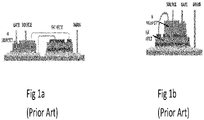
- Known examples of a side-by-side configuration and a stack-die configuration are shown in
Figure 1a and Figure 1b , respectively. - There are known GaN HEMT devices that are cascoded into various package types.
- It is also known in the art that for typical power module constructions, instead of discrete packages, multiple bare die are generally used so to achieve more flexible and more effective layout within a limited area on a module substrate. To further enhance the performance and size reduction, a stack-die is the development trend. However, supply of stack-die directly will pose many technical challenges including the known good die (KGD) issue.
- A known semiconductor device is described in
US9721944B2 - As shown in
Figure 2 , a hybrid semiconductor bipolar switch is implemented by die-mounting a high-voltage normally-on bipolar switch chip and a low-voltage normally-off FET chip side-by-side on a metallized ceramic substrate board. Connections between the chips and to the substrate are made by a wire-bonding. The ceramic material may be, for example, aluminum nitride, aluminum oxide, silicon nitride, or a similar material. The metallization on the ceramic board may be, for example, direct-bonded copper (DBC), actively-brazed copper (ABC), a molybdenum-based alloy, etc., any of which may be combined with titanium, tungsten, nickel, platinum, and/or gold coatings to facilitate die-attach and/or prevent inter-diffusion and oxidation of various metallization layers. Similarly, various coatings may be overlayed on the semiconductor chips where they are to be attached and/or bonded. - A hybrid switch may also be implemented as a "stacked" device by directly mounting a low-voltage normally-off FET chip onto a bonding pad of a high-voltage normally-on bipolar switch chip.
Figure 2 is a cross-sectional view of an example of such a device. As depicted inFigure 2 , a normally-onbipolar switch chip 301 has abonding pad 305 for a low voltage, high-current connection. Thebonding pad 305 is connected to the emitter of an IGBT onchip 301.Chip 301 is attached to ametallic surface 310 using adie attach material 302, such as a solder or conductive adhesive. Themetallic surface 310 is partly of an insulating ceramic board or a lead-frame. A low-voltage normally-offFET chip 306 is mounted with adie attach material 304 onto thebonding pad 305. Agate terminal 309 of FETchip 306 is used for gate control of stacked cascode 200. Asource terminal 308 of FETchip 306 is connected to agate terminal 303 of the normally-onbipolar switch chip 301 via aninterconnect 307. In this configuration, parasitic series resistance and inductance of the high-current interconnect between normally-onbipolar switch 301 and low-voltage normally-offswitch 306 will be minimized, thereby reducing undesirable voltage overshoots during switching under high di/dt and dv/dt conditions. - Various example embodiments are directed to the disadvantage as described above and/or others which may become apparent from the following disclosure.
- According to an embodiment of this invention a semiconductor device comprises a first die (e.g. a GaN HEMT die) and a second die (e.g. a MOSFET die) positioned on the top of the first die. The second die is attached using a die attach adhesive or solder. The semiconductor device further comprises an encapsulant deposited on the top of the semiconductor device, which encapsulant is covering the first die and the second die. Metalized vias are created within the encapsulant, wherein the metalized vias are arranged to distribute terminals of the first die and the terminals of the second die to the top side of the semiconductor device.
- In an embodiment of the present invention a gate terminal of the MOSFET die, a source terminal of the MOSFET die, a gate terminal of the GaN HEMT die and a drain terminal of the GaN HEMT die are distributed via the metalized vias to the top side of the semiconductor device.
- The semiconductor device can be a power semiconductor device.
- The invention also relates to a method of producing a semiconductor device. The method comprises the steps:
- attach a first die (e.g. a GaN HEMT die) on a film carrier,
- attach a second die (e.g. a MOSFET die) on the first die using a die attach adhesive or solder,
- cure the die attach adhesive or solder,
- encapsulate the first die and the second die with a mold compound or other encapsulant,
- drill vias within the encapsulant with a laser to the first die and second die pads,
- metallize the vias, so to make electrical contacts for the first die and for the second die,
- sinter a thick Cu film on the encapsulant, so to create terminals of the semiconductor device, alternative metal material can be used, such as sinter a thick Ag film on the encapsulant.
- singulate the semiconductor device.
- The method can further comprise a step of depositing an organic solderability preservative on the thick Cu film so to prevent Cu oxidation.
- A novel package as described in the embodiment of the present invention has significant advantages:
- a package outline is suitable for relatively easy manufacturing in both, an integrated device manufacturing (IDM) and a customer module assembly.
- a foot print reduction is secured, e.g. from 12x12 (CCPAK) to 5x6 (near chip scale package)
- a final test and burn-in for KGD is enabled
- semiconductor package terminals can be designed for an advanced assembly, such as a flip chip, a Cu wire bonding, etc.
- The semiconductor package according to the embodiments of the present invention is suitable for use in a power module where a customer can connect multiple packages together for various specific power supply applications. Instead of a bare die, the package can support test and burn-in, and provide a KGD (known good die) solution to a customer. The near chip scale package also reduces foot print requirement within the limited space of a power module, with an improvement in electrical and thermal performance. The package terminals can work with different interconnect technologies in module assembly, and the terminal locations can be re-distributed for more flexible substrate layout.
- So that the manner in which the features of the present disclosure can be understood in detail, a more particular description is made with reference to embodiments, some of which are illustrated in the appended figures. It is to be noted, however, that the appended figures illustrate only typical embodiments and are therefore not to be considered limiting of its scope. The figures are for facilitating an understanding of the disclosure and thus are not necessarily drawn to scale. Advantages of the subject matter claimed will become apparent to those skilled in the art upon reading this description in conjunction with the accompanying figures, in which like reference numerals have been used to designate like elements, and in which:
-
Figures 1a and 1b show known semiconductor devices; -
Figure 2 shows a known semiconductor device; -
Figure 3 illustrates a semiconductor device according to an embodiment of the invention; -
Figure 4 illustrates a method of manufacturing a semiconductor device according to an embodiment of the invention; -
Figure 5 illustrates a semiconductor device according to an embodiment of the invention. -
Figures 6a and 6b illustrate semiconductor devices according to embodiments of the invention. -
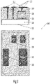
Figure 3 illustrates an embodiment of the present invention. Asemiconductor package 100 comprises a GaN HEMT die 104. The GaN HEMT comprises an exposed backside 102. A MOSFET die 108 is positioned on the top side of the GaN HEMT die 104, and it is attached to the GaN HEMT die 104 by a die attach adhesive orsolder 106. Anencapsulant 110 is deposed on the top of the whole semiconductor package, i.e. on the top of both the GaN HEMT die 104 and the MOSFET die 108. Within theencapsulant 110 there are laser drilled and metalizedvias 112. The Cu films of thepackage contact terminals 114 are placed on the top side of thesevias 112. Infigure 3 a top view of thesemiconductor package 100 is also shown. The gate terminal of the MOSFET die 120, the source terminal of the MOSFET die 122, the gate terminal of the GaN HEMT die 124, the drain terminal of the GaN HEMT die 126 are visible in said top view of the semiconductor device. - Although the embodiment shown in
Figure 3 relates to a GaN HEMT die and a MOSFET die, the invention also covers all kinds of wide-bandgap semiconductor devices and packages with a cascode operation. - The invention relates to a near chip scale packaging approach enabling KGD stack-die assembly in a power module, which is clearly advantageous compared to an individual bare die assembly or conventional discrete packages.
- The packaging according to the embodiments of the invention is suitable for packaging for WBG devices, for example D-mode GaN HEMT, SiC JFET, etc., which devices require cascoding of additional silicon MOSFET for safe normally-off operations. The semiconductor devices according to the embodiments of the present inventions are used in various products, e.g. a power module.
- The exemplary embodiment shown in
Figure 3 is just one of the possibilities covered by the present invention. The scope of the invention includes all similar embodiments and variations. - The exemplary embodiment shown in
Figure 3 , using the GaN HEMT die for illustration, has the following key features: - A driver die is attached to a power die in a stack-die configuration.
- The stack-die assembly is encapsulated, with an exposed back side of the power die, or exposed 5 sides in another design around.
- The contact pads of the driver and power die are connected to the package terminals by laser drilled and metallized vias.
- The package terminals are formed by Cu sintering or alternative metal sintering, using printing or dispensing method.
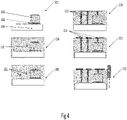
- An embodiment of the present invention is shown in
Figure 4 . A method of manufacturing a semiconductor package comprises steps: -
Reference sign 202 inFigure 4 :- ∘ attach a GaN HEMT die 104 on a film carrier
- ∘ attach a MOSFET die 108 on the GaN HEMT die 104 using a die attach adhesive 106
- ∘ cure the die attach material
-
Reference sign 204 inFigure 4 :
∘ encapsulate the stack-die assembly with a mold compound orother encapsulant 110 -
Reference sign 206 inFigure 4 :
∘ laser drill vias 112 to the die pads; multiple vias are possible to improve the performance of the semiconductor package -
Reference sign 208 inFigure 4 :
∘ metallize 113 the vias, making electrical contacts of the semiconductor package -
Reference sign 210 inFigure 4 :- ∘ sinter a thick Cu film on the
encapsulant 110, which creates thepackage terminal connections 114 to vias - ∘ organic solderability preservative (OSP) can be applied so to prevent Cu oxidation
- ∘ sinter a thick Cu film on the
-
Reference sign 212 inFigure 4 :
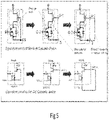
∘ singulate into individual units, e.g. a blade dicing - According to an embodiment of the present invention, within the cascode circuit, the source of the MOSFET die and the gate of the WBG die are connected together. Such a connection can be done on a module substrate surface. This is illustrated in
Figure 5 . - As shown in
Figure 6a , a stack-die package can be flip chip bonded onto a module substrate using known board mounting methods, e.g. soldering, sintering, etc. Compatible contact metallization will be applied. - Furthermore, as shown in
Figure 6b , a stack-die package can be bonded onto a module substrate using common die attach method. The pads can be connected to substrate using Cu wire bonding. - According to an embodiment of the invention, the gate contact can be relocated to the backside of the wafer, which provides more flexibility in interconnection.
- The invention is also applicable for vertical devices, e.g. a SiC FET. In this case the package back side is a drain pad.
- According to an embodiment of the invention, instead of a lead frame carrier, a stack-die assembly can be directly processed on wafer level.
- The invention also relates to a plurality of stack-die units. A dual stack-die package can be created by final singulation method. The dual stack-die can be further configured for specific application, e.g. a half-bridge, with new terminal pad geometry and connection routing on package top side, formed by new patterns of printed or dispensed Cu sintering materials.
- Particular and preferred aspects of the invention are set out in the accompanying independent claims. Combinations of features from the dependent and/or independent claims may be combined as appropriate and not merely as set out in the claims.
- The scope of the present disclosure includes any novel feature or combination of features disclosed therein either explicitly or implicitly or any generalisation thereof irrespective of whether or not it relates to the claimed invention or mitigate against any or all of the problems addressed by the present invention. The applicant hereby gives notice that new claims may be formulated to such features during prosecution of this application or of any such further application derived therefrom. In particular, with reference to the appended claims, features from dependent claims may be combined with those of the independent claims and features from respective independent claims may be combined in any appropriate manner and not merely in specific combinations enumerated in the claims.
- Features which are described in the context of separate embodiments may also be provided in combination in a single embodiment. Conversely, various features which are, for brevity, described in the context of a single embodiment, may also be provided separately or in any suitable sub combination.
- Term "comprising" does not exclude other elements or steps, the term "a" or "an" does not exclude a plurality. Reference signs in the claims shall not be construed as limiting the scope of the claims.
Claims (8)
- A semiconductor device comprising:- a first die,- a second die positioned on the top of the first die, the second die attached using a die attach adhesive or solder,- an encapsulant deposited on the top of the semiconductor device, which encapsulant is covering the first die and the second die,- metalized vias within the encapsulant, wherein the metalized vias are arranged to distribute terminals of the first die and the terminals of the second die to the top side of the semiconductor device.
- A semiconductor device as claimed in claim 1, wherein the first die is a GaN HEMT die.
- A semiconductor device as claimed in any of the previous claims, wherein the second die is a MOSFET die.
- A semiconductor device as claimed in claim 3, wherein a gate terminal of the MOSFET die, a source terminal of the MOSFET die, a gate terminal of the GaN HEMT die and a drain terminal of the GaN HEMT die are distributed via the metalized vias to the top side of the semiconductor device.
- A semiconductor device as claimed in any of the previous claims, wherein the semiconductor device is a power semiconductor device.
- A method of producing a semiconductor device, the method comprising the steps:- attach a first die on a film carrier,- attach a second die on the first die using a die attach adhesive or solder,- cure the die attach adhesive or solder,- encapsulate the first die and the second die with a mold compound or other encapsulant,- drill vias within the encapsulant with a laser to the first die and second die pads,- metallize the vias, so to make electrical contacts for the first die and for the second die,- sinter a thick Cu film or alternative metal film on the encapsulant, so to create terminals of the semiconductor device,- singulate the semiconductor device.
- A method of manufacturing a semiconductor device as claimed in claim 6, wherein the method comprises a step of depositing an organic solderability preservative on the thick Cu film so to prevent Cu oxidation.
- A method of manufacturing a semiconductor device as claimed in claims 6 and 7, wherein the fist die is a GaN HEMT die, and wherein the second die is a MOSFET die
Priority Applications (3)
| Application Number | Priority Date | Filing Date | Title |
|---|---|---|---|
| EP21154945.6A EP4040472A1 (en) | 2021-02-03 | 2021-02-03 | A semiconductor device and a method of manufacturing a semiconductor device |
| CN202210111341.0A CN114864528A (en) | 2021-02-03 | 2022-01-29 | Semiconductor device and method for manufacturing semiconductor device |
| US17/591,408 US12512450B2 (en) | 2021-02-03 | 2022-02-02 | Semiconductor device and a method of manufacturing a semiconductor device |
Applications Claiming Priority (1)
| Application Number | Priority Date | Filing Date | Title |
|---|---|---|---|
| EP21154945.6A EP4040472A1 (en) | 2021-02-03 | 2021-02-03 | A semiconductor device and a method of manufacturing a semiconductor device |
Publications (1)
| Publication Number | Publication Date |
|---|---|
| EP4040472A1 true EP4040472A1 (en) | 2022-08-10 |
Family
ID=74553571
Family Applications (1)
| Application Number | Title | Priority Date | Filing Date |
|---|---|---|---|
| EP21154945.6A Pending EP4040472A1 (en) | 2021-02-03 | 2021-02-03 | A semiconductor device and a method of manufacturing a semiconductor device |
Country Status (3)
| Country | Link |
|---|---|
| US (1) | US12512450B2 (en) |
| EP (1) | EP4040472A1 (en) |
| CN (1) | CN114864528A (en) |
Families Citing this family (4)
| Publication number | Priority date | Publication date | Assignee | Title |
|---|---|---|---|---|
| US12015010B2 (en) * | 2021-03-31 | 2024-06-18 | Taiwan Semiconductor Manufacturing Company Limited | Vertically stacked semiconductor device including a hybrid bond contact junction circuit and methods of forming the same |
| US20240056035A1 (en) * | 2022-08-12 | 2024-02-15 | Skyworks Solutions, Inc. | Apparatus and methods for amplifier linearization |
| CN116631985A (en) * | 2023-05-25 | 2023-08-22 | 广东致能科技有限公司 | A kind of semiconductor device and its preparation method |
| CN116913911B (en) * | 2023-09-05 | 2023-12-22 | 深圳智芯微电子科技有限公司 | Cascaded GaN HEMT packaging device and preparation method thereof |
Citations (4)
| Publication number | Priority date | Publication date | Assignee | Title |
|---|---|---|---|---|
| US20120187565A1 (en) * | 2011-01-25 | 2012-07-26 | Henrik Ewe | Device Including Two Semiconductor Chips and Manufacturing Thereof |
| US20120211892A1 (en) * | 2011-02-22 | 2012-08-23 | Stats Chippac, Ltd. | Semiconductor Device and Method of Forming WLCSP Structure Using Protruded MLP |
| US9721944B2 (en) | 2013-10-30 | 2017-08-01 | United Silicon Carbide, Inc. | Hybrid wide-bandgap semiconductor bipolar switches |
| US20200020638A1 (en) * | 2018-07-12 | 2020-01-16 | Samsung Electronics Co., Ltd. | Semiconductor package |
Family Cites Families (3)
| Publication number | Priority date | Publication date | Assignee | Title |
|---|---|---|---|---|
| TWI470549B (en) * | 2012-04-20 | 2015-01-21 | Insyde Software Corp | A method of using an image recognition guide to install an application, and an electronic device |
| US9735078B2 (en) * | 2014-04-16 | 2017-08-15 | Infineon Technologies Ag | Device including multiple semiconductor chips and multiple carriers |
| US10410952B2 (en) * | 2016-12-15 | 2019-09-10 | Infineon Technologies Ag | Power semiconductor packages having a substrate with two or more metal layers and one or more polymer-based insulating layers for separating the metal layers |
-
2021
- 2021-02-03 EP EP21154945.6A patent/EP4040472A1/en active Pending
-
2022
- 2022-01-29 CN CN202210111341.0A patent/CN114864528A/en active Pending
- 2022-02-02 US US17/591,408 patent/US12512450B2/en active Active
Patent Citations (4)
| Publication number | Priority date | Publication date | Assignee | Title |
|---|---|---|---|---|
| US20120187565A1 (en) * | 2011-01-25 | 2012-07-26 | Henrik Ewe | Device Including Two Semiconductor Chips and Manufacturing Thereof |
| US20120211892A1 (en) * | 2011-02-22 | 2012-08-23 | Stats Chippac, Ltd. | Semiconductor Device and Method of Forming WLCSP Structure Using Protruded MLP |
| US9721944B2 (en) | 2013-10-30 | 2017-08-01 | United Silicon Carbide, Inc. | Hybrid wide-bandgap semiconductor bipolar switches |
| US20200020638A1 (en) * | 2018-07-12 | 2020-01-16 | Samsung Electronics Co., Ltd. | Semiconductor package |
Also Published As
| Publication number | Publication date |
|---|---|
| US20220246595A1 (en) | 2022-08-04 |
| US12512450B2 (en) | 2025-12-30 |
| CN114864528A (en) | 2022-08-05 |
Similar Documents
| Publication | Publication Date | Title |
|---|---|---|
| US12512450B2 (en) | Semiconductor device and a method of manufacturing a semiconductor device | |
| US9177888B2 (en) | Electrically isolated power semiconductor package with optimized layout | |
| US11495580B2 (en) | Multi-chip module including stacked power devices with metal clip | |
| US9159720B2 (en) | Semiconductor module with a semiconductor chip and a passive component and method for producing the same | |
| US20060151868A1 (en) | Package for gallium nitride semiconductor devices | |
| US11004777B2 (en) | Semiconductor device assemblies | |
| KR102172689B1 (en) | Semiconductor package and method of fabricating the same | |
| CN216871961U (en) | Semiconductor device with a plurality of semiconductor chips | |
| CN103426837B (en) | Semiconductor packages and the method for forming semiconductor packages | |
| EP3690937B1 (en) | Cascode semiconductor device and method of manufacture | |
| US20250149432A1 (en) | Packaged electronic devices having dielectric substrates with thermally conductive adhesive layers | |
| CN111244061B (en) | Packaging structure of GaN devices | |
| US20220102253A1 (en) | Semiconductor package and method of manufacturing a semiconductor package | |
| US20240105544A1 (en) | Package with electrically insulating and thermally conductive layer on top of electronic component | |
| EP2309538A2 (en) | Package for semiconductor devices | |
| JP2023174214A (en) | semiconductor equipment | |
| CN202977407U (en) | Semiconductor module | |
| EP4421868B1 (en) | Semiconductor module arrangement | |
| US20250218914A1 (en) | Package with component-carrying intermediate structure and additional carrier having reference potential structure | |
| US20250293217A1 (en) | Embedded package with stacked semiconductor dies | |
| US20250218887A1 (en) | Semiconductor device and manufacturing method of semiconductor device | |
| US20260068694A1 (en) | Semiconductor Devices and Methods for Manufacturing Thereof | |
| US20260053007A1 (en) | Package with Thinner and Thicker Carriers for Carrying and Connecting Electronic Component |
Legal Events
| Date | Code | Title | Description |
|---|---|---|---|
| PUAI | Public reference made under article 153(3) epc to a published international application that has entered the european phase |
Free format text: ORIGINAL CODE: 0009012 |
|
| STAA | Information on the status of an ep patent application or granted ep patent |
Free format text: STATUS: THE APPLICATION HAS BEEN PUBLISHED |
|
| AK | Designated contracting states |
Kind code of ref document: A1 Designated state(s): AL AT BE BG CH CY CZ DE DK EE ES FI FR GB GR HR HU IE IS IT LI LT LU LV MC MK MT NL NO PL PT RO RS SE SI SK SM TR |
|
| STAA | Information on the status of an ep patent application or granted ep patent |
Free format text: STATUS: REQUEST FOR EXAMINATION WAS MADE |
|
| 17P | Request for examination filed |
Effective date: 20230209 |
|
| RBV | Designated contracting states (corrected) |
Designated state(s): AL AT BE BG CH CY CZ DE DK EE ES FI FR GB GR HR HU IE IS IT LI LT LU LV MC MK MT NL NO PL PT RO RS SE SI SK SM TR |