EP4038661B1 - Utilisation d'un matériau à transition de spin pour mesurer et/ou limiter la température de composants électroniques/photoniques - Google Patents
Utilisation d'un matériau à transition de spin pour mesurer et/ou limiter la température de composants électroniques/photoniques Download PDFInfo
- Publication number
- EP4038661B1 EP4038661B1 EP20780228.1A EP20780228A EP4038661B1 EP 4038661 B1 EP4038661 B1 EP 4038661B1 EP 20780228 A EP20780228 A EP 20780228A EP 4038661 B1 EP4038661 B1 EP 4038661B1
- Authority
- EP
- European Patent Office
- Prior art keywords
- temperature
- component
- spin
- circuit
- spin transition
- Prior art date
- Legal status (The legal status is an assumption and is not a legal conclusion. Google has not performed a legal analysis and makes no representation as to the accuracy of the status listed.)
- Active
Links
Images


Classifications
-
- G—PHYSICS
- G01—MEASURING; TESTING
- G01K—MEASURING TEMPERATURE; MEASURING QUANTITY OF HEAT; THERMALLY-SENSITIVE ELEMENTS NOT OTHERWISE PROVIDED FOR
- G01K11/00—Measuring temperature based upon physical or chemical changes not covered by groups G01K3/00, G01K5/00, G01K7/00 or G01K9/00
- G01K11/12—Measuring temperature based upon physical or chemical changes not covered by groups G01K3/00, G01K5/00, G01K7/00 or G01K9/00 using changes in colour, translucency or reflectance
- G01K11/125—Measuring temperature based upon physical or chemical changes not covered by groups G01K3/00, G01K5/00, G01K7/00 or G01K9/00 using changes in colour, translucency or reflectance using changes in reflectance
-
- H—ELECTRICITY
- H10—SEMICONDUCTOR DEVICES; ELECTRIC SOLID-STATE DEVICES NOT OTHERWISE PROVIDED FOR
- H10W—GENERIC PACKAGES, INTERCONNECTIONS, CONNECTORS OR OTHER CONSTRUCTIONAL DETAILS OF DEVICES COVERED BY CLASS H10
- H10W40/00—Arrangements for thermal protection or thermal control
- H10W40/20—Arrangements for cooling
- H10W40/25—Arrangements for cooling characterised by their materials
-
- G—PHYSICS
- G01—MEASURING; TESTING
- G01K—MEASURING TEMPERATURE; MEASURING QUANTITY OF HEAT; THERMALLY-SENSITIVE ELEMENTS NOT OTHERWISE PROVIDED FOR
- G01K11/00—Measuring temperature based upon physical or chemical changes not covered by groups G01K3/00, G01K5/00, G01K7/00 or G01K9/00
- G01K11/12—Measuring temperature based upon physical or chemical changes not covered by groups G01K3/00, G01K5/00, G01K7/00 or G01K9/00 using changes in colour, translucency or reflectance
- G01K11/14—Measuring temperature based upon physical or chemical changes not covered by groups G01K3/00, G01K5/00, G01K7/00 or G01K9/00 using changes in colour, translucency or reflectance of inorganic materials
Definitions
- the present invention relates to the measurement and limitation of temperature (to avoid overheating phenomena) in electronic components.
- temperature to avoid overheating phenomena
- microelectronics With the development of new technologies and the increase in telecommunications speeds, there is clearly a growing need (1) for the rapid detection of "hot spots" (industrial diagnosis) that can deteriorate the performance of these devices and (2) for the development of simple solutions to limit their consequences.
- the overheating of electronic components constitutes a major problem affecting many electronic cards installed in various devices such as servers, computers, tablets, mobile phones and connected objects to name a few.
- the consequences of this overheating can range from a simple slowdown of software, to a breakdown and even irreversible deterioration of devices in the worst case.
- Temperature measurement on electronic devices is typically performed by infrared thermography, thermoreflectance, Raman microscopy, scanning thermal microscopy, or fluorescence thermometry.
- Limiting the temperature of components is typically achieved by the use of cooling systems to overcome overheating problems. These include air, water or solid-liquid phase change (MCP) cooling systems.
- Air cooling systems are the most commonly used. There are two types: passive and active. The passive system consists of a simple radiator that facilitates the free circulation of air near the heating elements. In the majority of cases, this system is not enough and it is associated with a fan (active system) which evacuates the hot air outside the case of a computer for example. A water or refrigerant circuit limits the temperature rise within the box.
- the spin transition phenomenon is accompanied by a change in optical properties (absorption, optical index), magnetic, mechanical and dielectric, allowing, in the case of thermochromic materials, a significant and reversible color change under the effect of 'a variation in temperature. It is a reversible transition between low-spin and high-spin electronic states that occurs within certain transition metal complexes, and which corresponds to an intramolecular electronic reconfiguration. Furthermore, the transition from the low-spin state to the high-spin state is an endothermic process (the compound stores heat).
- the invention concerns the use of said spin transition material to measure (thermometry) and limit (thermal inertia) a temperature rise, particularly in the field of electronics.
- the spin transition materials which may be suitable for the invention have a spin transition temperature of between 40°C and 100°C, in particular between 50 and 70°C.
- said spin transition material is [Fe(HB(1,2,4-triazol-1-yl) 3 ) 2 ], bis[hydrotris(1,2,4-triazol-1-yl)borate]iron (II).
- the synthesis of this material was published in 1994 ( Chem. Ber., 1994, 127, 1379 ) and spin transition properties measured in 1996 ( Chem. Eur. J., 1996, 2, 992-1000 ). However, the application of this material in the field of microelectronics had never been considered.
- This material is, moreover, sublimable, thus allowing its deposition on the components.
- the materials according to the invention exhibit an abrupt spin transition.
- the abrupt nature of the transition defines the temperature range over which each transition occurs. According to the invention, we define as “abrupt” a transition in which 80% of the change in spin state takes place over a temperature range below 10°C.
- the width of the hysteresis defines the temperature difference between the low spin to high spin (heating) and high spin to low spin (cooling) transitions.
- the spin transition takes place “without thermal hysteresis”, that is to say, such that the width of the hysteresis is typically less than 1°C.
- said material can be deposited in the form of a continuous and homogeneous thin layer with a thickness of between 10 nm and 10 ⁇ m, on at least part of the surface of said component.
- Said material can be sublimated such that thin films of a few tens of nanometers to several micrometers thick can be made on different substrates/circuits. These films are the site of a stable and abrupt spin transition.
- electronic or photonic component suitable for the invention we mean an element intended to be assembled with others in order to carry out one or more electronic or photonic functions, and which is likely to undergo an increase in temperature, during its operation. functioning.
- passive or active components we can in particular cite diodes, transistors, integrated circuits, resistors, capacitors, coils, etc.
- photonic components we can cite laser diodes and any other device based on the engineering of optical indices at the interfaces, giving the latter great sensitivity to any temperature variation.
- the present invention also relates to an electronic circuit or a photonic device comprising at least one component according to the invention.
- the present invention also relates to a process for preparing a component according to the invention comprising the step of depositing said spin transition material in a thin layer, for example by sublimation or spin coating, on all or part of said component.
- the deposit can thus be made by the method described in the article J. Mater. Chem. C, 2017, 5, 4419 , to obtain thin films in which the transition properties of the material are preserved.
- Sublimation deposition is a vapor phase deposition technique, under vacuum, which allows obtaining a thin layer of controlled thickness.
- Deposition by spin coating can be carried out by application or adaptation of the process described in EP 1 430 552 .
- the deposition conditions as well as the intrinsic properties of said material are non-destructive for the properties and performances of the electronic or photonic component and/or circuit.
- the present invention also relates to the use of a spin transition material as defined above for measuring and/or limiting a temperature rise in an electronic component and/or circuit or photonics.
- the use according to the invention is based on the measurement of an optical property of the spin transition material. This constitutes a simple, non-invasive and cost-effective method that can provide thermal imaging with good temporal and spatial resolution. This makes it possible to establish a precise and reproducible thermal map of electronic and/or photonic nano-components.
- optical property one can in particular measure the optical index, the optical reflectivity or the optical absorbance.
- the measurement of the optical property can be carried out with a spatial resolution making it possible to reach a few hundred nanometers (diffraction limit).
- steps b) and c) can be repeated at different base temperatures below Tmax, by increasing and/or decreasing the temperature of said component and/or circuit, and a mapping of the temperature of said component and/or circuit is established.
- the use according to the invention is based on the heat storage properties of said material to cushion a transient rise in temperature generated by an electronic component overheating due to of its intensive operation or if it is defective.
- the use according to the invention combines the advantages of a passive system (silent technology that does not consume energy) and the efficiency of an active system.
- the physical principle used is that of the endothermic transition. This principle is generally used via solid-liquid phase change (MCP) materials. According to the invention, this principle is exploited with a molecular material with spin transition, without change of state (fusion), and therefore, more stable, more viable (avoiding sealing problems) and also non-flammable.
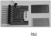
- FIG. 2 shows a photograph of the electrical connector (left) and test device used in Example 1, consisting of a substrate (20 ⁇ 10 mm) of silicon (top right) or glass (bottom right) on which 7 gold nano-wires are produced.
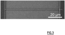
- FIG. 3 represents a scanning electron microscopy image of a gold nanowire (width: 1 ⁇ m, length: 80 ⁇ m, thickness: 50 nm).
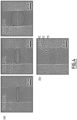
- FIG. 4 illustrates the thermometry measurements carried out on a nano-wire of the test device covered by a layer of [Fe(HB(1,2,4-triazol-1-yl) 3 ) 2 ] 200 nm thick:
- FIG. 5 illustrates the temperature limitation measurements of a gold nanowire of the test device (glass substrate) covered by a layer of [Fe(HB(1,2,4-triazol-1-yl) 3 ) 2 ] of 900 nm thick: Evolution of ⁇ T wire , measured 30 ⁇ s after the injection of the 20 mA electric current, as a function of the base temperature for the active compound (Fe complex, [Fe(HB(1,2, 4-triazol-1-yl) 3 ) 2 ]) as well as for a similar but inactive compound (Zn complex, [Zn(HB(1,2,4-triazol-1-yl) 3 ) 2 ]).
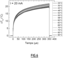
- FIG. 6 represents the rise in temperature ( ⁇ T wire ) experienced by a gold nano-wire (on a glass substrate) over time following the sudden injection of an electric current of 20 mA for 350 ⁇ s, for different base temperatures of the device.
- the material transition is accompanied by a significant change in the optical properties of the thin film, in particular the optical absorbance ( Figure 1a ), optical reflectivity ( Figure 1b ) or the optical index ( Figure 1c ). This allows the use of different optical techniques to detect the spin transition.
- This transition is also accompanied by an enthalpy of change of state (latent heat) of the order of 33 kJ/kg (endothermic transition during the passage of the low-spin state towards the high-spin state (heating) and exothermic otherwise (cooling)).
- This last property can therefore be used to significantly limit a transient increase in temperature.
- the temperature and transition properties of the thin films of said material are not significantly affected even after more than 10,000 thermal cycles in ambient air.
- Thermal mapping of an electronic circuit was carried out with a spatial resolution of the order of a micrometer by a series of optical reflectivity measurements.
- the experimental protocol consists of recording the image of the device covered with said material under an optical microscope (in reflectivity mode) before and after powering up the microcircuit.
- this experimental protocol was validated on a test device which consists of gold nanowires (width: 1 ⁇ m, length: 80 ⁇ m, thickness: 50 nm) produced by electronic lithography and photolithography on silicon substrates or glass. This entire device was covered by a thin film 200 nm thick of said material, deposited by thermal evaporation under vacuum.
- the injection of a direct electric current of 4 mA, using a source meter (Keithley 2611A) and a suitable connector, causes the nano-wire to heat up by the Joule effect.
- the temperature rise of the wire ⁇ T wire could be measured over time for different base temperatures of the device, controlled by a heating/cooling system (Linkam Scientific LTS120).
- the heating of the wire measured 30 ⁇ s after the injection of the current, shows a minimum when the base temperature of the wire is close to the transition temperature. This reduction in the heating of the wire occurs because part of the heat released by the wire has been absorbed by the spin transition material.
- Zn complex [Zn(HB(1,2,4-triazol-1-yl) 3 ) 2 ]
Landscapes
- Physics & Mathematics (AREA)
- General Physics & Mathematics (AREA)
- Chemical & Material Sciences (AREA)
- Inorganic Chemistry (AREA)
- Photometry And Measurement Of Optical Pulse Characteristics (AREA)
- Measuring Temperature Or Quantity Of Heat (AREA)
- Investigating Or Analyzing Materials Using Thermal Means (AREA)
- Radiation Pyrometers (AREA)
Description
- La présente invention concerne la mesure et la limitation de la température (pour éviter les phénomènes de surchauffe) dans les composants électroniques.
Dans le domaine de la microélectronique, avec le développement des nouvelles technologies et l'augmentation des débits de télécommunication, il y a clairement un besoin grandissant (1) pour la détection rapide de « points chauds » (diagnostic industriel) pouvant détériorer la performance de ces dispositifs et (2) pour le développement de solutions simples pour en limiter les conséquences. En effet, actuellement, la surchauffe des composants électroniques constitue un problème majeur affectant de nombreuses cartes électroniques implantées dans divers appareils comme les serveurs, les ordinateurs, les tablettes, les téléphones portables et les objets connectés pour ne citer qu'eux. Les conséquences de cette surchauffe peuvent aller d'un simple ralentissement des logiciels, à une panne et même à la détérioration irréversible des appareils dans le pire des cas. Il existe donc un fort besoin dans le domaine de la microélectronique pour analyser et limiter la surchauffe des composants. - La mesure de la température sur les dispositifs électroniques est généralement effectuée par thermographie infrarouge, thermoréflectance, microscopie Raman, microscopie thermique à balayage ou thermométrie par fluorescence.
La limitation de la température des composants (aussi appelée l'inertie thermique) est typiquement réalisée par l'utilisation de systèmes de refroidissement afin de pallier aux problèmes de surchauffe. On trouve notamment des systèmes de refroidissement à air, à eau ou des matériaux à changement de phase solide-liquide (MCP). Les systèmes de refroidissement à air sont les plus couramment utilisés. Il en existe deux types : passif et actif. Le système passif est composé d'un simple radiateur qui facilite la libre circulation de l'air près des éléments chauffants. Dans la majorité des cas, ce système ne suffit pas et il est associé à un ventilateur (système actif) qui évacue l'air chaud à l'extérieur du boitier d'un ordinateur par exemple. Un circuit à eau ou à fluide frigorigène permet de limiter la hausse de température au sein du boitier. Ces systèmes à eau ou à changement de phase apparaissent trop coûteux, dangereux et souvent peu adaptés à cause de problèmes d'étanchéité pour être utilisés très largement dans les appareils électroniques destinés au grand public. De plus, outre le fait qu'ils soient trop encombrants pour être intégrés dans certains ordinateurs portables ultraplats ou tablettes, ces systèmes s'avèrent peu efficaces. - Il n'existe pas de solution simple, stable et peu coûteuse pour réaliser de façon intégrée une mesure d'élévation de température rapide et/ou une limitation de celle-ci. Il existe donc un réel besoin de trouver un système intégrable, peu encombrant et flexible (sans forme prédéfinie) afin de sonder et d'éviter la surchauffe des composants électroniques présents dans les objets du quotidien.
- Les articles J. Mater. Chem., 2010, 20, 5499-5503, J. Mater. Chem., 2012, 22, 3745, Small, 2016, 12, 6325, et les proceedings du 16TH INTERNATIONAL WORKSHOP ON THERMAL INVESTIGATIONS OF ICS AND SYSTEMS, octobre 2010 rapportent la possibilité d'utiliser un matériau à transition de spin (éventuellement en le combinant avec une sonde fluorescente) pour des applications dans le domaine de la micro- et nano-thermométrie.
- Néanmoins, il reste à mettre à oeuvre pour ces applications un matériau présentant des propriétés exceptionnelles de stabilité thermique et de résilience lors de sa mise en forme et de son cyclage thermique, dont les propriétés énergétiques combinées aux propriétés de transition thermique permettent son utilisation à titre de sonde thermique et de limitation de température.
- Il a maintenant été découvert que ces utilisations pouvaient être mises en oeuvre avec un matériau à transition de spin, présentant des propriétés spécifiques, notamment de mise en forme, de résilience et de stabilité thermique, permettant les applications visées.
- Ainsi, selon un premier objet, la présente invention concerne donc un composant électronique ou photonique comprenant un film déposé sur tout ou partie dudit composant, ledit film comprenant un matériau à transition de spin, caractérisé en ce que le matériau à transition de spin présente les propriétés suivantes :
- a. Ledit matériau présente une transition de spin à une température comprise entre 40 et 100°C avec une largeur d'hystérésis inférieure à 1°C,
- b. La stabilité de ladite température de transition de spin au cyclage est supérieure à 10 000 cycles thermiques avec une reproductibilité inférieure ou égale à 1°C;
- c. Ledit matériau est sublimable.
- Le phénomène de transition de spin s'accompagne d'un changement des propriétés optiques (absorption, indice optique), magnétiques, mécaniques et diélectriques, permettant, dans le cas de matériaux thermochromes, un changement de couleur significatif et réversible sous l'effet d'une variation de température. Il s'agit d'une transition réversible entre les états électroniques bas-spin et haut-spin qui se produit au sein de certains complexes de métaux de transition, et qui correspond à une reconfiguration électronique intramoléculaire. Par ailleurs, le passage de l'état bas-spin vers l'état haut-spin est un processus endothermique (le composé emmagasine de la chaleur).
- Il s'agit donc d'utiliser un composé à transition de spin en particulier dans le domaine de la microélectronique, pour d'une part (1) sonder localement la température de composants électroniques en fonctionnement et notamment une élévation indésirable de température par une mesure (imagerie) optique (micro-thermométrie) et d'autre part (2) limiter/amortir cette augmentation de température en utilisant les propriétés endothermiques intrinsèques du matériau (inertie thermique) ; ces deux applications pouvant être réalisées simultanément avec le même matériau dit multifonctionnel.
- L'invention concerne la mise en oeuvre dudit matériau à transition de spin pour mesurer (thermométrie) et limiter (inertie thermique) une élévation de température notamment dans le domaine de l'électronique.
- Typiquement, les matériaux à transition de spin pouvant convenir à l'invention présentent une température à transition de spin comprise entre 40°C et 100°C, notamment entre 50 et 70°C.
- Avantageusement, ledit matériau à transition de spin est [Fe(HB(1,2,4-triazol-1-yl)3)2], bis[hydrotris(1,2,4-triazol-1-yl)borate]fer(II). La synthèse de ce matériau a été publiée en 1994 (Chem. Ber., 1994, 127, 1379) et les propriétés de transition de spin mesurées en 1996 (Chem. Eur. J., 1996, 2, 992-1000). Néanmoins, l'application de ce matériau dans le domaine de la microélectronique n'avait jamais été considérée.
- Ce matériau présente une température de transition de spin Tmax = 62°C, idéale pour la détection des points chauds en microélectronique, avec une transition abrupte le rendant ainsi compatible avec des mesures thermométriques, associé, de façon inattendue, à une stabilité thermique et une non-fatigabilité au cours de cycles thermiques répétés. Ce matériau est, de plus, sublimable, permettant ainsi son dépôt sur les composants.
- Typiquement, les matériaux selon l'invention présentent une transition de spin abrupte.
Le caractère abrupte de la transition définit la plage de température sur laquelle s'opère chacune des transitions. On définit selon l'invention comme « abrupte » une transition dont 80% du changement de l'état de spin s'opère sur une gamme de température inférieure à 10°C. - La largeur de l'hystérésis définit l'écart de température entre les transitions bas spin vers haut spin (chauffage) et haut spin vers bas spin (refroidissement).
- Avantageusement, selon l'invention, la transition de spin s'opère « sans hystérésis thermique », c'est-à-dire, telle que la largeur de l'hystérésis est typiquement inférieure à 1°C.
- Selon un mode de réalisation, ledit matériau peut être déposé sous la forme d'une couche mince continue et homogène d'épaisseur comprise entre 10 nm et 10 µm, sur au moins une partie de la surface dudit composant.
- Ledit matériau peut être sublimé de telle sorte que des films minces de quelques dizaines de nanomètres à plusieurs micromètres d'épaisseur peuvent être réalisés sur différents substrats/circuits. Ces films sont le siège d'une transition de spin stable et abrupte.
- A titre de composant électronique ou photonique convenant à l'invention, on entend un élément destiné à être assemblé avec d'autres afin de réaliser une ou plusieurs fonctions électroniques ou photoniques, et qui est susceptible de subir une augmentation de température, lors de son fonctionnement. On peut notamment citer les composants passifs ou actifs, et plus particulièrement les diodes, transistors, circuits intégrés, résistances, condensateurs, bobines, etc. En ce qui concerne les composants photoniques, on peut citer les diodes laser et tout autre dispositif basé sur une ingénierie des indices optiques aux interfaces, conférant à ces derniers une grande sensibilité à toute variation de température.
- Selon un autre objet, la présente invention concerne également un circuit électronique ou un dispositif photonique comprenant au moins un composant selon l'invention.
- Selon un autre objet, la présente invention concerne également un procédé de préparation d'un composant selon l'invention comprenant l'étape de dépôt dudit matériau à transition de spin en couche mince, par exemple par sublimation ou spin coating, sur tout ou partie dudit composant. Le dépôt peut ainsi être effectué par la méthode décrite dans l'article J. Mater. Chem. C, 2017, 5, 4419, pour obtenir des films minces dans lesquels les propriétés de transition du matériau sont préservées.
- Le dépôt par sublimation est une technique de dépôt en phase vapeur, sous vide, qui permet l'obtention d'une couche mince d'épaisseur contrôlée. Le dépôt par spin coating peut être effectué par application ou adaptation du procédé décrit dans
EP 1 430 552 . - Les conditions de dépôt ainsi que les propriétés intrinsèques dudit matériau sont non destructives pour les propriétés et les performances du composant et/ou circuit électronique ou photonique.
- Selon un autre objet, la présente invention concerne également l'utilisation d'un matériau à transition de spin tel que défini ci-avant pour la mesure et/ou la limitation d'une élévation de température dans un composant et/ou circuit électronique ou photonique.
- Pour ce qui concerne la mesure de l'augmentation de la température, l'utilisation selon l'invention repose sur la mesure d'une propriété optique du matériau à transition de spin. Ceci constitue une méthode simple, non invasive et rentable qui peut fournir une imagerie thermique avec une bonne résolution temporelle et spatiale. Ceci permet d'établir de façon précise et reproductible une cartographique thermique de nano-composants électroniques et/ou photoniques.
- A titre de propriété optique, on peut notamment mesurer l'indice optique, la réflectivité optique ou l'absorbance optique.
- Avantageusement, la mesure de la propriété optique peut être effectuée avec une résolution spatiale permettant d'atteindre quelques centaines de nanomètres (limite de diffraction).
- Ainsi, selon un objet, la présente invention concerne un procédé de mesure d'une élévation de la température au-delà d'une température Tmax au sein d'un composant et/ou d'un circuit électronique ou photonique tel que défini ci-avant et tel que la température de transition de spin du matériau est égale à Tmax,
ledit procédé comprenant : - a. La mesure d'au moins une propriété optique dudit matériau lorsque ledit composant et/ou circuit est hors fonctionnement,
- b. La mesure d'au moins une propriété optique dudit matériau lorsque ledit composant et/ou circuit est en fonctionnement,
- c. L'identification des zones pour lesquelles ladite propriété optique varie par suite de la transition de spin dudit matériau.
- Selon un mode de réalisation, les étapes b) et c) peuvent être répétées à différentes températures de base au-dessous de Tmax, en augmentant et/ou diminuant la température dudit composant et/ou circuit, et qu'une cartographie de la température dudit composant et/ou circuit est établie.
- Pour ce qui concerne la limitation de l'augmentation de la température, l'utilisation selon l'invention repose sur les propriétés d'emmagasinement de la chaleur par ledit matériau pour amortir une élévation transitoire de température générée par un composant électronique en surchauffe à cause de son fonctionnement intensif ou s'il est défectueux. L'utilisation selon l'invention allie les avantages d'un système passif (technologie silencieuse non consommatrice en énergie) et l'efficacité d'un système actif. Le principe physique exploité est celui de la transition endothermique. Ce principe est généralement utilisé via les matériaux à changement de phase solide - liquide (MCP). Selon l'invention, ce principe est exploité avec un matériau moléculaire à transition de spin, sans changement d'état (fusion), et par conséquent, plus stable, plus viable (évitant des problèmes d'étanchéité) et également non inflammable.
- Ainsi, selon un autre objet, la présente invention concerne un procédé de limitation de la température dans un composant et/ou circuit électronique ou photonique tel que défini ci-avant, en deçà d'une température Tmax, telle que Tmax est égale à la température de transition de spin dudit matériau,
ledit procédé comprenant : - a. La montée en température dudit composant et/ou circuit lors de son fonctionnement,
- b. Lorsque ladite température atteint la valeur Tmax, ledit matériau subit une transition de spin endothermique vers la phase haut spin absorbant tout ou partie de l'énergie de surchauffe et limitant ainsi l'élévation de la température jusqu'à la transformation complète dudit matériau vers la phase haut-spin.
- La
Figure 1 représente l'évolution de propriétés optiques d'un film mince de [Fe(HB(1,2,4-triazol-1-yl)3)2] de 200 nm d'épaisseur en fonction de la température : (a) Absorption optique (λ = 317 nm) en fonction de la température mesurée après 4, 1858 et 10321 cycles thermiques. Ces mesures démontrent la grande résilience du matériau, dont la température de transition reste invariante (ΔT < 1°C) après plus de 10.000 cycles thermiques. (b) Réflectivité optique (λ = 452 nm) mesurée sur un film mince déposé sur un substrat de verre, montrant une variation relative de la réflectivité de -5,8 % lors de la transition de l'état bas-spin vers l'état haut-spin. (c) Variation de l'indice optique du film mince (mesurée à λ = 500 nm) en fonction de la température. - La
Figure 2 représente une photographie du connecteur électrique (à gauche) et du dispositif d'essai utilisé dans l'exemple 1, consistant en un substrat (20 × 10 mm) de silicium (en haut à droite) ou de verre (en bas à droite) sur lesquels sont élaborés 7 nano-fils d'or. - La
Figure 3 représente une image en microscopie électronique à balayage d'un nano-fil d'or (largeur : 1 µm, longueur : 80 µm, épaisseur : 50 nm). - La
Figure 4 illustre les mesures de thermométrie effectuées sur un nano-fil du dispositif d'essai recouvert par une couche de [Fe(HB(1,2,4-triazol-1-yl)3)2] de 200 nm d'épaisseur : (a) Images en réflectivité (λ = 452 nm) obtenues par microscopie optique du nano-fil en fonctionnement sur un substrat de verre (parcouru par un courant électrique de 4 mA) à différentes températures de base (Ta = 30°C, 40°C et 50°C) et tracé des lignes isothermes, (b) Carte de températures obtenue lors du fonctionnement du nano-fil d'or chauffé par effet Joule. - La
Figure 5 illustre les mesures de limitation de température d'un nano-fil d'or du dispositif d'essai (substrat en verre) recouvert par une couche de [Fe(HB(1,2,4-triazol-1-yl)3)2] de 900 nm d'épaisseur : Evolution de ΔTfil, mesuré 30 µs après l'injection du courant électrique de 20 mA, en fonction de la température de base pour le composé actif (complexe de Fe, [Fe(HB(1,2,4-triazol-1-yl)3)2]) ainsi que pour un composé similaire, mais inactif (complexe de Zn, [Zn(HB(1,2,4-triazol-1-yl)3)2]). - La
Figure 6 représente l'élévation de la température (ΔTfil) subit par un nano-fil d'or (sur un substrat de verre) au cours du temps suite à l'injection brusque d'un courant électrique de 20 mA pendant 350 µs, pour différentes températures de base du dispositif. - Les exemples suivants illustrent de façon non limitative la présente invention.
-
- 1. Préparation du matériau
Ledit matériau est synthétisé suivant le protocole décrit dans l'article Chem. Ber., 1994, 127, 1379. - 2. Dépôt sur un composant
Le dépôt du film mince de [Fe(HB(1,2,4-triazol-1-yl)3)2] sur le dispositif d'essai a été effectué par évaporation thermique dans une chambre de dépôt sous vide PREVAC à une pression d'environ 2 × 10⁻⁷ mbar. La poudre du composé a d'abord été purifiée par sublimation, puis évaporée à 250°C à une vitesse de 0,03 Å / s. La vitesse d'évaporation et l'épaisseur du film ont été contrôlées in situ par une microbalance à quartz. Les films obtenus font ensuite l'objet d'un traitement sous vapeur d'eau qui permet d'obtenir des films nano-cristallins, stables et homogènes [J. Mater. Chem. C, 2017, 5, 4419]. - 3. Mise en évidence des propriétés thermométriques
- Comme illustré en
Figure 1 , la transition du matériau s'accompagne d'un changement significatif des propriétés optiques du film mince, en particulier de l'absorbance optique (Figure 1a ), de la réflectivité optique (Figure 1b ) ou encore de l'indice optique (Figure 1c ). Ceci permet l'utilisation de différentes techniques optiques pour détecter la transition de spin. - Cette transition s'accompagne également d'une enthalpie de changement d'état (chaleur latente) de l'ordre de 33 kJ/kg (transition endothermique lors du passage de l'état bas-spin vers l'état haut-spin (chauffage) et exothermique dans le cas contraire (refroidissement)). Cette dernière propriété peut donc être utilisée pour limiter significativement une augmentation transitoire de température.
- Comme montré sur la
Figure 1a , la température et les propriétés de transition des films minces dudit matériau ne sont pas significativement affectées même après plus de 10.000 cycles thermiques à l'air ambiant. - Une cartographie thermique d'un circuit électronique a été réalisée avec une résolution spatiale de l'ordre du micromètre par une série de mesures de réflectivité optique. Le protocole expérimental consiste à enregistrer l'image du dispositif recouvert dudit matériau sous microscope optique (en mode réflectivité) avant et après la mise sous tension du microcircuit.
- Comme le montre la
Figure 2 , ce protocole expérimental a été validé sur un dispositif d'essai qui consiste en des nano-fils d'or (largeur : 1 µm, longueur : 80 µm, épaisseur : 50 nm) élaborés par lithographie électronique et photolithographie sur des substrats de silicium ou de verre. L'ensemble de ce dispositif a été recouvert par un film mince de 200 nm d'épaisseur dudit matériau, déposé par évaporation thermique sous vide. L'injection d'un courant électrique continu de 4 mA, à l'aide d'un source-mètre (Keithley 2611A) et d'un connecteur adapté, engendre l'échauffement du nano-fil par effet Joule. Des images du dispositif sont enregistrées en réflectivité (λ = 452 nm), avant et pendant son fonctionnement, grâce à un microscope optique (Olympus BX51) équipé d'un objectif ×50 (ouverture numérique NA = 0,5) et d'une caméra CCD (Andor Technology Clara, 1392 × 1040 pixels de taille 6,45 µm). Dans l'image de réflectivité optique du nano-fil en fonctionnement, deux zones sont alors discernables (Figure 3 ) : une zone, proche du fil, dont la réflectivité a changé lors de l'injection du courant et dont la température se trouve donc au-delà de la température de transition ; et une zone dont la réflectivité optique reste inchangée. Ces deux zones sont séparées par une ligne isotherme pour laquelle l'augmentation de température correspond exactement à la différence entre la température de transition dudit matériau (Tm) et la température ambiante (Ta). Un des avantages de cette méthode est que la détermination de l'augmentation de température sur cette ligne isotherme peut être réalisée sans aucune calibration préalable de la réflectivité. Par la suite, un chauffage ou un refroidissement de l'ensemble du microcircuit - ce dernier étant posé sur un système de chauffage/refroidissement (Linkam Scientific LTS 120) - à différentes `températures de base' Ta permet d'enregistrer autant de lignes isothermes que désirées. L'ensemble de ces lignes isothermes peut ensuite être regroupé dans une carte de températures (Figure 4 ). - Cette propriété de 'limitation de température' a été démontrée sur le même dispositif d'essai consistant en un nano-fil d'or sur un substrat en verre, recouvert d'un film mince dudit matériau, et chauffé par effet Joule suite à l'injection brusque d'un courant électrique de 20 mA (
Figures 5 et6 ). Au cours de cette expérience, l'augmentation de température du fil a pu être déterminée précisément au cours du temps (avec une résolution temporelle de l'ordre de la µs) en mesurant la variation temporelle de la résistance électrique du fil (qui varie linéairement avec sa température) à l'aide d'un dispositif de mesure de résistance différentielle fabriqué sur mesure [Microelectronics Journal 46 (2015) 1167-1174]. Comme montré dans laFigure 6 , l'élévation de température du fil ΔTfil a pu être mesurée au cours du temps pour différentes températures de base du dispositif, contrôlées par un système de chauffage/refroidissement (Linkam Scientific LTS120). Comme le montre laFigure 5 , l'échauffement du fil, mesuré 30 µs après l'injection du courant, montre un minimum lorsque la température de base du fil est proche de la température de transition. Cette réduction de l'échauffement du fil s'opère car une partie de la chaleur dégagée par le fil a été absorbée par le matériau à transition de spin. La même expérience réalisée lorsque le nano-fil est recouvert par un composé similaire mais inactif (complexe de Zn, [Zn(HB(1,2,4-triazol-1-yl)3)2]), montre un comportement linéaire dans l'échauffement du fil en fonction de la température de base (Figure 5 ).
Claims (10)
- Composant électronique ou photonique comprenant un film déposé sur tout ou partie dudit composant, ledit film comprenant un matériau à transition de spin, caractérisé en ce que le matériau à transition de spin présente les propriétés suivantes :a. Ledit matériau présente une transition de spin à une température comprise entre 40 et 100°C avec une largeur d'hystérésis inférieure à 1°C,b. La stabilité de ladite température de transition de spin au cyclage est supérieure à 10 000 cycles thermiques avec une reproductibilité inférieure ou égale à 1°C;c. Ledit matériau est sublimable.
- Composant selon la revendication 1 tel que ledit matériau à transition de spin est [Fe(HB(1,2,4-triazol-1-yl)3)2].
- Composant selon la revendication 1 ou 2 tel que ledit matériau est déposé sous la forme d'une couche mince continue et homogène d'épaisseur comprise entre 10 nm et 10 µm, sur au moins une partie de sa surface.
- Circuit électronique ou dispositif photonique comprenant au moins un composant selon l'une quelconque des revendications 1 à 3.
- Procédé de préparation d'un composant selon l'une quelconque des revendications 1 à 3 comprenant l'étape de dépôt dudit matériau par sublimation ou spin coating sur tout ou partie dudit composant.
- Utilisation d'un matériau à transition de spin tel que défini en revendication 1 ou 2 pour la mesure et/ou la limitation d'une élévation de température dans un composant et/ou circuit électronique ou photonique.
- Procédé de limitation de la température dans un composant et/ou circuit électronique ou photonique tel que défini selon l'une quelconque des revendications 1 à 4, en deçà d'une température Tmax, telle que Tmax est égale à la température de transition de spin dudit matériau,
ledit procédé comprenant :a. La montée en température dudit composant et/ou circuit lors de son fonctionnement,b. Lorsque ladite température atteint la valeur Tmax, ledit matériau subit une transition de spin endothermique vers la phase haut spin absorbant tout ou partie de l'énergie de surchauffe et limitant ainsi l'élévation de la température jusqu'à la transformation complète dudit matériau vers la phase haut-spin. - Procédé de mesure d'une élévation de la température au-delà d'une température Tmax au sein d'un composant et/ou d'un circuit électronique ou photonique tel que défini selon l'une quelconque des revendications 1 à 4 et tel que la température de transition de spin du matériau est égale à Tmax,
ledit procédé comprenant :a. La mesure d'au moins une propriété optique dudit matériau lorsque ledit composant et/ou circuit est hors fonctionnement,b. La mesure d'au moins une propriété optique dudit matériau lorsque ledit composant et/ou circuit est en fonctionnement,c. L'identification des zones pour lesquelles ladite propriété optique varie par suite de la transition de spin dudit matériau. - Procédé selon la revendication 8 tel que les étapes b) et c) sont répétées à différentes températures de base au-dessous de Tmax, en augmentant et/ou diminuant la température dudit composant et/ou circuit, et qu'une cartographie de la température dudit composant et/ou circuit est établie.
- Procédé selon la revendication 8 ou 9 tel qu'on mesure une ou plusieurs propriétés optiques choisies parmi l'indice optique, la réflectivité optique et l'absorbance optique.
Applications Claiming Priority (2)
| Application Number | Priority Date | Filing Date | Title |
|---|---|---|---|
| FR1910886A FR3101479B1 (fr) | 2019-10-01 | 2019-10-01 | Utilisation d’un matériau à transition de spin pour mesurer et/ou limiter la température de composants électroniques/photoniques |
| PCT/EP2020/077495 WO2021064094A1 (fr) | 2019-10-01 | 2020-10-01 | Utilisation d'un matériau à transition de spin pour mesurer et/ou limiter la température de composants électroniques/photoniques |
Publications (3)
| Publication Number | Publication Date |
|---|---|
| EP4038661A1 EP4038661A1 (fr) | 2022-08-10 |
| EP4038661C0 EP4038661C0 (fr) | 2023-11-08 |
| EP4038661B1 true EP4038661B1 (fr) | 2023-11-08 |
Family
ID=69572062
Family Applications (1)
| Application Number | Title | Priority Date | Filing Date |
|---|---|---|---|
| EP20780228.1A Active EP4038661B1 (fr) | 2019-10-01 | 2020-10-01 | Utilisation d'un matériau à transition de spin pour mesurer et/ou limiter la température de composants électroniques/photoniques |
Country Status (6)
| Country | Link |
|---|---|
| US (1) | US12566097B2 (fr) |
| EP (1) | EP4038661B1 (fr) |
| JP (1) | JP2022550566A (fr) |
| ES (1) | ES2972703T3 (fr) |
| FR (1) | FR3101479B1 (fr) |
| WO (1) | WO2021064094A1 (fr) |
Family Cites Families (7)
| Publication number | Priority date | Publication date | Assignee | Title |
|---|---|---|---|---|
| FR2829293B1 (fr) | 2001-08-31 | 2003-11-14 | Centre Nat Rech Scient | Memoire moleculaire et son procede de fabrication |
| FR2937561B1 (fr) * | 2008-10-23 | 2010-12-31 | Centre Nat Rech Scient | Procede de delimitation d'une aire de sport ou de jeu au moyen d'un materiau a transition de spin thermochrome |
| US8326426B2 (en) * | 2009-04-03 | 2012-12-04 | Enteromedics, Inc. | Implantable device with heat storage |
| FR2963015B1 (fr) | 2010-07-22 | 2012-09-07 | Centre Nat Rech Scient | Procede de photocommutation thermique de materiaux a transition de spin et applications |
| JPWO2014033827A1 (ja) | 2012-08-28 | 2016-08-08 | 日立オートモティブシステムズ株式会社 | 二次電池 |
| FR3017209B1 (fr) | 2014-02-03 | 2017-04-28 | Univ Bordeaux | Procede et systeme de visualisation d'un rayonnement electromagnetique infrarouge emis par une source |
| US10297300B2 (en) | 2014-09-21 | 2019-05-21 | Samsung Electronics Co., Ltd. | Method and system for determining temperature using a magnetic junction |
-
2019
- 2019-10-01 FR FR1910886A patent/FR3101479B1/fr active Active
-
2020
- 2020-10-01 JP JP2022520303A patent/JP2022550566A/ja active Pending
- 2020-10-01 US US17/765,532 patent/US12566097B2/en active Active
- 2020-10-01 WO PCT/EP2020/077495 patent/WO2021064094A1/fr not_active Ceased
- 2020-10-01 ES ES20780228T patent/ES2972703T3/es active Active
- 2020-10-01 EP EP20780228.1A patent/EP4038661B1/fr active Active
Also Published As
| Publication number | Publication date |
|---|---|
| US20220341792A1 (en) | 2022-10-27 |
| EP4038661A1 (fr) | 2022-08-10 |
| WO2021064094A1 (fr) | 2021-04-08 |
| EP4038661C0 (fr) | 2023-11-08 |
| FR3101479A1 (fr) | 2021-04-02 |
| ES2972703T3 (es) | 2024-06-14 |
| US12566097B2 (en) | 2026-03-03 |
| FR3101479B1 (fr) | 2021-10-15 |
| JP2022550566A (ja) | 2022-12-02 |
Similar Documents
| Publication | Publication Date | Title |
|---|---|---|
| Ridier et al. | Unprecedented switching endurance affords for high-resolution surface temperature mapping using a spin-crossover film | |
| Uǧur et al. | A near‐infrared mechano responsive polymer system | |
| Glamazda et al. | Achieving high mid‐IR bolometric responsivity for anisotropic composite materials from carbon nanotubes and polymers | |
| Schrickx et al. | Ultra‐high alignment of polymer semiconductor blends enabling photodetectors with exceptional polarization sensitivity | |
| Kwan et al. | Nanoscale calorimetry of isolated polyethylene single crystals | |
| Zhang et al. | Bandgap engineering of BiIns Nanowire for wide‐spectrum, high‐responsivity, and polarimetric‐sensitive detection | |
| Zang et al. | Synthesis of single‐layer graphene on nickel using a droplet CVD process | |
| Lee et al. | Rapid and facile formation of P3HT organogels via spin coating: Tuning functional properties of organic electronic thin films | |
| Yu et al. | Refractive‐Index‐Matching‐Based Encryption of Photonic Crystal Prints with Multistage and Reconfigurable Information | |
| Yarimaga et al. | Thermofluorescent Conjugated Polymer Sensors for Nano‐and Microscale Temperature Monitoring | |
| Chen et al. | Greatly Enhanced Radiative Transfer Enabled by Hyperbolic Phonon Polaritons in α‐MoO3 | |
| Yu et al. | Composition Waves in Solution‐Processed Organic Films and Its Propagations from Kinetically Frozen Surface Mesophases | |
| van Son et al. | Highly Ordered Supramolecular Materials of Phase‐Separated Block Molecules for Long‐Range Exciton Transport | |
| EP4038661A1 (fr) | Utilisation d'un matériau à transition de spin pour mesurer et/ou limiter la température de composants électroniques/photoniques | |
| De Albuquerque et al. | Photopyroelectric spectroscopy of polyaniline films | |
| Srivastava et al. | Fabrication of highly responsive phase-change Ge2Sb2Te5 photodetector for visible region: V Srivastava et al. | |
| Goyal et al. | Aromatic pendant containing conjugated polydiacetylene based low‐temperature irreversible thermochromic indicator: smart monitoring of milk storage | |
| Maurya et al. | Direct Laser Write‐Read‐Erase in a Functional Molecular Phase Change Material–Polymer Nanocomposite Thin Film | |
| Leontie et al. | Electric and optical properties of some new functional lower-rim-substituted calixarene derivatives in thin films | |
| FR2530017A1 (fr) | Thermistance-bolometre et procede pour la realiser | |
| Cetin et al. | Unraveling the synthesis, characterization, and optical behaviors of thin films: a comprehensive study | |
| Shim et al. | Temperature behavior of dielectric function spectra and optical transitions in TlGaS2 | |
| Jian et al. | Effects of isomeric transformation on characteristics of Alq3 amorphous layers prepared by vacuum deposition at various substrate temperatures | |
| Raj Mohan et al. | Charge transport properties of MDMO PPV thin films cast in different solvents | |
| Khachadorian et al. | The morphology of silicon nanowire samples: a Raman study |
Legal Events
| Date | Code | Title | Description |
|---|---|---|---|
| STAA | Information on the status of an ep patent application or granted ep patent |
Free format text: STATUS: UNKNOWN |
|
| STAA | Information on the status of an ep patent application or granted ep patent |
Free format text: STATUS: THE INTERNATIONAL PUBLICATION HAS BEEN MADE |
|
| PUAI | Public reference made under article 153(3) epc to a published international application that has entered the european phase |
Free format text: ORIGINAL CODE: 0009012 |
|
| STAA | Information on the status of an ep patent application or granted ep patent |
Free format text: STATUS: REQUEST FOR EXAMINATION WAS MADE |
|
| 17P | Request for examination filed |
Effective date: 20220330 |
|
| AK | Designated contracting states |
Kind code of ref document: A1 Designated state(s): AL AT BE BG CH CY CZ DE DK EE ES FI FR GB GR HR HU IE IS IT LI LT LU LV MC MK MT NL NO PL PT RO RS SE SI SK SM TR |
|
| DAV | Request for validation of the european patent (deleted) | ||
| DAX | Request for extension of the european patent (deleted) | ||
| GRAP | Despatch of communication of intention to grant a patent |
Free format text: ORIGINAL CODE: EPIDOSNIGR1 |
|
| STAA | Information on the status of an ep patent application or granted ep patent |
Free format text: STATUS: GRANT OF PATENT IS INTENDED |
|
| INTG | Intention to grant announced |
Effective date: 20230612 |
|
| GRAS | Grant fee paid |
Free format text: ORIGINAL CODE: EPIDOSNIGR3 |
|
| GRAA | (expected) grant |
Free format text: ORIGINAL CODE: 0009210 |
|
| STAA | Information on the status of an ep patent application or granted ep patent |
Free format text: STATUS: THE PATENT HAS BEEN GRANTED |
|
| AK | Designated contracting states |
Kind code of ref document: B1 Designated state(s): AL AT BE BG CH CY CZ DE DK EE ES FI FR GB GR HR HU IE IS IT LI LT LU LV MC MK MT NL NO PL PT RO RS SE SI SK SM TR |
|
| REG | Reference to a national code |
Ref country code: GB Ref legal event code: FG4D Free format text: NOT ENGLISH |
|
| REG | Reference to a national code |
Ref country code: CH Ref legal event code: EP |
|
| REG | Reference to a national code |
Ref country code: DE Ref legal event code: R096 Ref document number: 602020020786 Country of ref document: DE |
|
| REG | Reference to a national code |
Ref country code: IE Ref legal event code: FG4D Free format text: LANGUAGE OF EP DOCUMENT: FRENCH |
|
| U01 | Request for unitary effect filed |
Effective date: 20231208 |
|
| U07 | Unitary effect registered |
Designated state(s): AT BE BG DE DK EE FI FR IT LT LU LV MT NL PT SE SI Effective date: 20231221 |
|
| PG25 | Lapsed in a contracting state [announced via postgrant information from national office to epo] |
Ref country code: GR Free format text: LAPSE BECAUSE OF FAILURE TO SUBMIT A TRANSLATION OF THE DESCRIPTION OR TO PAY THE FEE WITHIN THE PRESCRIBED TIME-LIMIT Effective date: 20240209 |
|
| PG25 | Lapsed in a contracting state [announced via postgrant information from national office to epo] |
Ref country code: IS Free format text: LAPSE BECAUSE OF FAILURE TO SUBMIT A TRANSLATION OF THE DESCRIPTION OR TO PAY THE FEE WITHIN THE PRESCRIBED TIME-LIMIT Effective date: 20240308 |
|
| PG25 | Lapsed in a contracting state [announced via postgrant information from national office to epo] |
Ref country code: IS Free format text: LAPSE BECAUSE OF FAILURE TO SUBMIT A TRANSLATION OF THE DESCRIPTION OR TO PAY THE FEE WITHIN THE PRESCRIBED TIME-LIMIT Effective date: 20240308 Ref country code: GR Free format text: LAPSE BECAUSE OF FAILURE TO SUBMIT A TRANSLATION OF THE DESCRIPTION OR TO PAY THE FEE WITHIN THE PRESCRIBED TIME-LIMIT Effective date: 20240209 |
|
| PG25 | Lapsed in a contracting state [announced via postgrant information from national office to epo] |
Ref country code: RS Free format text: LAPSE BECAUSE OF FAILURE TO SUBMIT A TRANSLATION OF THE DESCRIPTION OR TO PAY THE FEE WITHIN THE PRESCRIBED TIME-LIMIT Effective date: 20231108 Ref country code: PL Free format text: LAPSE BECAUSE OF FAILURE TO SUBMIT A TRANSLATION OF THE DESCRIPTION OR TO PAY THE FEE WITHIN THE PRESCRIBED TIME-LIMIT Effective date: 20231108 Ref country code: NO Free format text: LAPSE BECAUSE OF FAILURE TO SUBMIT A TRANSLATION OF THE DESCRIPTION OR TO PAY THE FEE WITHIN THE PRESCRIBED TIME-LIMIT Effective date: 20240208 Ref country code: HR Free format text: LAPSE BECAUSE OF FAILURE TO SUBMIT A TRANSLATION OF THE DESCRIPTION OR TO PAY THE FEE WITHIN THE PRESCRIBED TIME-LIMIT Effective date: 20231108 |
|
| REG | Reference to a national code |
Ref country code: ES Ref legal event code: FG2A Ref document number: 2972703 Country of ref document: ES Kind code of ref document: T3 Effective date: 20240614 |
|
| PG25 | Lapsed in a contracting state [announced via postgrant information from national office to epo] |
Ref country code: CZ Free format text: LAPSE BECAUSE OF FAILURE TO SUBMIT A TRANSLATION OF THE DESCRIPTION OR TO PAY THE FEE WITHIN THE PRESCRIBED TIME-LIMIT Effective date: 20231108 |
|
| PG25 | Lapsed in a contracting state [announced via postgrant information from national office to epo] |
Ref country code: SK Free format text: LAPSE BECAUSE OF FAILURE TO SUBMIT A TRANSLATION OF THE DESCRIPTION OR TO PAY THE FEE WITHIN THE PRESCRIBED TIME-LIMIT Effective date: 20231108 |
|
| PG25 | Lapsed in a contracting state [announced via postgrant information from national office to epo] |
Ref country code: SM Free format text: LAPSE BECAUSE OF FAILURE TO SUBMIT A TRANSLATION OF THE DESCRIPTION OR TO PAY THE FEE WITHIN THE PRESCRIBED TIME-LIMIT Effective date: 20231108 Ref country code: SK Free format text: LAPSE BECAUSE OF FAILURE TO SUBMIT A TRANSLATION OF THE DESCRIPTION OR TO PAY THE FEE WITHIN THE PRESCRIBED TIME-LIMIT Effective date: 20231108 Ref country code: RO Free format text: LAPSE BECAUSE OF FAILURE TO SUBMIT A TRANSLATION OF THE DESCRIPTION OR TO PAY THE FEE WITHIN THE PRESCRIBED TIME-LIMIT Effective date: 20231108 Ref country code: CZ Free format text: LAPSE BECAUSE OF FAILURE TO SUBMIT A TRANSLATION OF THE DESCRIPTION OR TO PAY THE FEE WITHIN THE PRESCRIBED TIME-LIMIT Effective date: 20231108 |
|
| REG | Reference to a national code |
Ref country code: DE Ref legal event code: R097 Ref document number: 602020020786 Country of ref document: DE |
|
| PLBE | No opposition filed within time limit |
Free format text: ORIGINAL CODE: 0009261 |
|
| STAA | Information on the status of an ep patent application or granted ep patent |
Free format text: STATUS: NO OPPOSITION FILED WITHIN TIME LIMIT |
|
| 26N | No opposition filed |
Effective date: 20240809 |
|
| U20 | Renewal fee for the european patent with unitary effect paid |
Year of fee payment: 5 Effective date: 20241022 |
|
| REG | Reference to a national code |
Ref country code: CH Ref legal event code: PL |
|
| PG25 | Lapsed in a contracting state [announced via postgrant information from national office to epo] |
Ref country code: MC Free format text: LAPSE BECAUSE OF FAILURE TO SUBMIT A TRANSLATION OF THE DESCRIPTION OR TO PAY THE FEE WITHIN THE PRESCRIBED TIME-LIMIT Effective date: 20231108 |
|
| PG25 | Lapsed in a contracting state [announced via postgrant information from national office to epo] |
Ref country code: CH Free format text: LAPSE BECAUSE OF NON-PAYMENT OF DUE FEES Effective date: 20241031 |
|
| U20 | Renewal fee for the european patent with unitary effect paid |
Year of fee payment: 6 Effective date: 20250909 |
|
| PG25 | Lapsed in a contracting state [announced via postgrant information from national office to epo] |
Ref country code: IE Free format text: LAPSE BECAUSE OF NON-PAYMENT OF DUE FEES Effective date: 20241001 |
|
| PGFP | Annual fee paid to national office [announced via postgrant information from national office to epo] |
Ref country code: GB Payment date: 20251023 Year of fee payment: 6 |
|
| PG25 | Lapsed in a contracting state [announced via postgrant information from national office to epo] |
Ref country code: CY Free format text: LAPSE BECAUSE OF FAILURE TO SUBMIT A TRANSLATION OF THE DESCRIPTION OR TO PAY THE FEE WITHIN THE PRESCRIBED TIME-LIMIT; INVALID AB INITIO Effective date: 20201001 |
|
| PGFP | Annual fee paid to national office [announced via postgrant information from national office to epo] |
Ref country code: ES Payment date: 20251110 Year of fee payment: 6 |
|
| PG25 | Lapsed in a contracting state [announced via postgrant information from national office to epo] |
Ref country code: HU Free format text: LAPSE BECAUSE OF FAILURE TO SUBMIT A TRANSLATION OF THE DESCRIPTION OR TO PAY THE FEE WITHIN THE PRESCRIBED TIME-LIMIT; INVALID AB INITIO Effective date: 20201001 |