EP4037302A1 - Imaging device and moving body - Google Patents
Imaging device and moving body Download PDFInfo
- Publication number
- EP4037302A1 EP4037302A1 EP20870200.1A EP20870200A EP4037302A1 EP 4037302 A1 EP4037302 A1 EP 4037302A1 EP 20870200 A EP20870200 A EP 20870200A EP 4037302 A1 EP4037302 A1 EP 4037302A1
- Authority
- EP
- European Patent Office
- Prior art keywords
- substrate
- connector
- imaging
- housing
- connector substrate
- Prior art date
- Legal status (The legal status is an assumption and is not a legal conclusion. Google has not performed a legal analysis and makes no representation as to the accuracy of the status listed.)
- Granted
Links
Images


Classifications
-
- G—PHYSICS
- G03—PHOTOGRAPHY; CINEMATOGRAPHY; ANALOGOUS TECHNIQUES USING WAVES OTHER THAN OPTICAL WAVES; ELECTROGRAPHY; HOLOGRAPHY
- G03B—APPARATUS OR ARRANGEMENTS FOR TAKING PHOTOGRAPHS OR FOR PROJECTING OR VIEWING THEM; APPARATUS OR ARRANGEMENTS EMPLOYING ANALOGOUS TECHNIQUES USING WAVES OTHER THAN OPTICAL WAVES; ACCESSORIES THEREFOR
- G03B17/00—Details of cameras or camera bodies; Accessories therefor
- G03B17/02—Bodies
- G03B17/08—Waterproof bodies or housings
-
- H—ELECTRICITY
- H04—ELECTRIC COMMUNICATION TECHNIQUE
- H04N—PICTORIAL COMMUNICATION, e.g. TELEVISION
- H04N23/00—Cameras or camera modules comprising electronic image sensors; Control thereof
- H04N23/50—Constructional details
-
- B—PERFORMING OPERATIONS; TRANSPORTING
- B60—VEHICLES IN GENERAL
- B60R—VEHICLES, VEHICLE FITTINGS, OR VEHICLE PARTS, NOT OTHERWISE PROVIDED FOR
- B60R11/00—Arrangements for holding or mounting articles, not otherwise provided for
- B60R11/04—Mounting of cameras operative during drive; Arrangement of controls thereof relative to the vehicle
-
- G—PHYSICS
- G03—PHOTOGRAPHY; CINEMATOGRAPHY; ANALOGOUS TECHNIQUES USING WAVES OTHER THAN OPTICAL WAVES; ELECTROGRAPHY; HOLOGRAPHY
- G03B—APPARATUS OR ARRANGEMENTS FOR TAKING PHOTOGRAPHS OR FOR PROJECTING OR VIEWING THEM; APPARATUS OR ARRANGEMENTS EMPLOYING ANALOGOUS TECHNIQUES USING WAVES OTHER THAN OPTICAL WAVES; ACCESSORIES THEREFOR
- G03B15/00—Special procedures for taking photographs; Apparatus therefor
- G03B15/006—Apparatus mounted on flying objects
-
- G—PHYSICS
- G03—PHOTOGRAPHY; CINEMATOGRAPHY; ANALOGOUS TECHNIQUES USING WAVES OTHER THAN OPTICAL WAVES; ELECTROGRAPHY; HOLOGRAPHY
- G03B—APPARATUS OR ARRANGEMENTS FOR TAKING PHOTOGRAPHS OR FOR PROJECTING OR VIEWING THEM; APPARATUS OR ARRANGEMENTS EMPLOYING ANALOGOUS TECHNIQUES USING WAVES OTHER THAN OPTICAL WAVES; ACCESSORIES THEREFOR
- G03B17/00—Details of cameras or camera bodies; Accessories therefor
- G03B17/02—Bodies
-
- G—PHYSICS
- G03—PHOTOGRAPHY; CINEMATOGRAPHY; ANALOGOUS TECHNIQUES USING WAVES OTHER THAN OPTICAL WAVES; ELECTROGRAPHY; HOLOGRAPHY
- G03B—APPARATUS OR ARRANGEMENTS FOR TAKING PHOTOGRAPHS OR FOR PROJECTING OR VIEWING THEM; APPARATUS OR ARRANGEMENTS EMPLOYING ANALOGOUS TECHNIQUES USING WAVES OTHER THAN OPTICAL WAVES; ACCESSORIES THEREFOR
- G03B30/00—Camera modules comprising integrated lens units and imaging units, specially adapted for being embedded in other devices, e.g. mobile phones or vehicles
-
- H—ELECTRICITY
- H04—ELECTRIC COMMUNICATION TECHNIQUE
- H04N—PICTORIAL COMMUNICATION, e.g. TELEVISION
- H04N23/00—Cameras or camera modules comprising electronic image sensors; Control thereof
- H04N23/50—Constructional details
- H04N23/51—Housings
-
- H—ELECTRICITY
- H04—ELECTRIC COMMUNICATION TECHNIQUE
- H04N—PICTORIAL COMMUNICATION, e.g. TELEVISION
- H04N23/00—Cameras or camera modules comprising electronic image sensors; Control thereof
- H04N23/50—Constructional details
- H04N23/52—Elements optimising image sensor operation, e.g. for electromagnetic interference [EMI] protection or temperature control by heat transfer or cooling elements
-
- H—ELECTRICITY
- H04—ELECTRIC COMMUNICATION TECHNIQUE
- H04N—PICTORIAL COMMUNICATION, e.g. TELEVISION
- H04N23/00—Cameras or camera modules comprising electronic image sensors; Control thereof
- H04N23/50—Constructional details
- H04N23/54—Mounting of pick-up tubes, electronic image sensors, deviation or focusing coils
Definitions
- the present disclosure relates to an imaging apparatus and a mobile object.
- a known sealing structure prevents an impairment of performance of an accessory module of a camera by blocking entry of foreign matter into the accessory module and provides ease of maintenance (see, for example, Patent Literature 1).
- An imaging apparatus includes an imaging substrate, a connector substrate, and a housing.
- the imaging substrate is provided with an imaging device that produces image data.
- the connector substrate is movably connected to the imaging substrate.
- the connector substrate includes a terminal configured to be connectable in a first direction to an external connector to which the image data is output.
- the imaging substrate and the connector substrate are accommodated in the housing.
- the housing includes a restricting section that restricts a position of the connector substrate in the first direction.
- the connector substrate is configured to be movable within a predetermined range in a direction intersecting the first direction.
- a mobile object includes an imaging apparatus installed therein.
- the imaging apparatus includes an imaging substrate, a connector substrate, and a housing.
- the imaging substrate is provided with an imaging device that produces image data.
- the connector substrate is movably connected to the imaging substrate.
- the connector substrate includes a terminal configured to be connectable in a first direction to an external connector to which the image data is output.
- the imaging substrate and the connector substrate are accommodated in the housing.
- the housing includes a restricting section that restricts a position of the connector substrate in the first direction.
- the connector substrate is configured to be movable within a predetermined range in a direction intersecting the first direction.
- An imaging apparatus and a mobile object according to an embodiment of the present disclosure can ensure both ease of assembly and sealing performance.
- an imaging apparatus 1 includes a lens 58, a holding member 56, an imaging substrate 10, a connector substrate 20, and a housing 50.
- the imaging apparatus 1 may also include a first sheet metal 30.
- the first sheet metal 30 is also referred to as a sheet-metal member.
- the housing 50 has an internal space in which the lens 58, the holding member 56, the imaging substrate 10, the connector substrate 20, and the first sheet metal 30 are placed.
- the internal space of the housing 50 is defined by an inner wall surface 51 as illustrated in Figs. 1 and 2 .
- the housing 50 may be made of a material such as resin.
- the housing 50 may be made of resin or may be made of various materials.
- the imaging apparatus 1 captures, by an imaging device 12 mounted on the imaging substrate 10, an object image formed by the lens 58.
- the imaging device 12 produces image data upon capturing the object image.
- the imaging substrate 10 is connected to the connector substrate 20 and outputs the image data to the connector substrate 20.
- the imaging apparatus 1 is configured to be connectable to an external connector 80.
- the imaging apparatus 1 outputs the image data to an external apparatus through the external connector 80. That is, the imaging apparatus 1 outputs the image data to the external connector 80.
- the lens 58 is also referred to as an optical member.
- the lens 58 forms an object image incident on the imaging apparatus 1.
- the holding member 56 holds the lens 58.
- the lens 58 is joined to the holding member 56.
- Two or more lenses 58, instead of the lens 58, may be included. At least one of such lenses 58 may be replaced with another optical member, such as a mirror.
- the lens 58 may be bonded to the holding member 56 with, for example, an adhesive.
- the lens 58 may be joined to the holding member 56 via a fitting structure.
- the lens 58 may be joined to the holding member 56 by fastening with screws or the like.
- the imaging device 12 is mounted on the imaging substrate 10.
- the imaging device 12 has an imaging surface.
- the imaging substrate 10 is disposed so that the imaging surface of the imaging device 12 is located in an image-forming plane of the lens 58.
- An object image formed on the imaging surface by the lens 58 is captured by the imaging device 12.
- the imaging device 12 may, for example, be a complementary metal oxide semiconductor (CMOS) image sensor or a charge-coupled device (CCD).
- CMOS complementary metal oxide semiconductor
- CCD charge-coupled device
- a circuit for processing data output from the imaging device 12 may be mounted on the imaging substrate 10.
- the imaging substrate 10 may, for example, be a printed circuit board.
- the imaging substrate 10 is joined to the holding member 56.
- the imaging substrate 10 may be bonded to the holding member 56 with, for example, an adhesive.
- the imaging substrate 10 may be joined to the holding member 56 via a fitting structure.
- the imaging substrate 10 may be joined to the holding member 56 by fastening with screws or the like.
- the connector substrate 20 and the lens 58 are disposed on opposite sides with respect to the imaging substrate 10 therebetween. In other words, the connector substrate 20 is farther than the imaging substrate 10 when viewed from the lens 58.
- the connector substrate 20 is supported by the first sheet metal 30 on the negative side in the Z-axis direction.
- the first sheet metal 30 includes a base 36, which extends along the connector substrate 20.
- the first sheet metal 30 also includes substrate-supporting portions 38, which protrude from the base 36 toward the positive side in the Z-axis direction.
- the connector substrate 20 is supported on the positive side in the Z-axis direction of the substrate-supporting portions 38. That is, the first sheet metal 30 keeps the connector substrate 20 from shifting toward the negative side in the Z-axis direction.
- the first sheet metal 30 includes protrusions 34, which protrude from a side surface portion 32 to the positive side and the negative side in the X-axis direction.
- each protrusion 34 includes a restricted section 35, which is a surface on the negative side in the Z-axis direction.
- the housing 50 includes a restricting section 53, which is a surface on the positive side in the Z-axis direction of a portion protruding from the inner wall surface 51 toward the negative side in the X-axis direction (see Fig. 3 ).
- the restricted sections 35 of the first sheet metal 30 are in contact with the restricting section 53 of the housing 50 such that the first sheet metal 30 is kept from shifting toward the negative side in the Z-axis direction.
- the first sheet metal 30 includes the substrate-supporting portions 38 to keep the connector substrate 20 from shifting toward the negative side in the Z-axis direction. It can thus be said that the restricting section 53 of the housing 50 keeps the connector substrate 20 from shifting toward the negative side in the Z-axis direction.
- the side surface portion 32 of the first sheet metal 30 may have a cutout 35a.
- the cutout 35a is provided in the side surface portion 32 such that the side surface portion 32 includes the restricted section 35 oriented toward the negative side in the Z-axis direction.
- the restricted sections 35 of the first sheet metal 30 are also in contact with the restricting section 53 of the housing 50 such that the first sheet metal 30 is kept from shifting toward the negative side in the Z-axis direction.
- the side surface portion 32 of the first sheet metal 30 is elastic.
- the side surface portion 32 is configured to be capable of shifting away from the inner wall surface 51 of the housing 50 toward the inner side, with the bending point on the base 36 as a pivot point. Even when the side surface portion 32 includes the protrusions 34 protruding toward the inner wall surface 51, the first sheet metal 30 is more smoothly accommodated in the housing 50, because the side surface portion 32 shifts away from the inner wall surface 51 toward the inner side. Once the first sheet metal 30 is accommodated in the housing 50, the side surface portion 32 exerts elastic force toward the inner wall surface 51. The elastic force makes the first sheet metal 30 less prone to move in the Z-axis direction.
- the housing 50 has an end portion 52, which is located on the positive side in the Z-axis direction.
- the housing 50 has an opening defined by the end portion 52 on the positive side in the Z-axis direction.
- the internal space of the housing 50 communicates with the outside of the housing 50 through the opening.
- the connector substrate 20 is slid into the internal space of the housing 50 through the opening.
- the external connector 80 is inserted toward the negative side in the Z-axis direction and connected to the connector substrate 20 through the opening.
- the end portion 52 comes into contact with the external connector 80.
- the internal space of the housing 50 is sealed.
- the direction in which the external connector 80 is inserted into the imaging apparatus 1 is also referred to as a first direction.
- the connector substrate 20 has a first surface and a second surface that is opposite to the first surface.
- the first surface is oriented toward the positive side in the Z-axis direction
- the second surface is oriented toward the negative side in the Z-axis direction.
- the connector substrate 20 includes a terminal 22.
- the terminal 22 is mounted on the first surface of the connector substrate 20.
- the terminal 22 is configured to be connectable to a terminal 82 of the external connector 80.
- the terminal 82 of the external connector 80 is connected to the terminal 22 of the connector substrate 20 such that the terminal 82 presses the terminal 22 toward the negative side in the Z-axis direction. With the connector substrate 20 being kept from shifting toward the negative side in the Z-axis direction by the housing 50, the terminal 82 is easily connected to the terminal 22.
- the connector substrate 20 is not kept from shifting toward the negative side in the Z-axis direction, pressing the terminal 82 of the external connector 80 against the terminal 22 of the connector substrate 20 does not ensure connection between the external connector 80 and the connector substrate 20.
- the connector substrate 20 needs to be connected to the external connector 80 before being accommodated in the housing 50; that is, the connector substrate 20 needs to be accommodated in the housing 50 after being connected to the external connector 80.
- This connection procedure may be a constraint on the assembly of the imaging apparatus 1.
- the present embodiment enables connection of the external connector 80 to the connector substrate 20 in a state in which the connector substrate 20 is accommodated in the housing 50. As a result, a higher degree of flexibility is achieved in assembling the imaging apparatus 1.
- the connector substrate 20 includes an end portion 24.
- the inner wall surface 51 of the housing 50 is disposed at a predetermined distance or more from the end portion 24 of the connector substrate 20.
- the connector substrate 20 is thus movable within a predetermined distance range in the X-axis direction and the Y-axis direction. That is, the connector substrate 20 is movable within the predetermined range in a direction intersecting the Z-axis.
- the inner wall surface 51 of the housing 50 is larger in size than the connector substrate 20 in plan view in the Z-axis direction. In this case, the connector substrate 20 is movable within the predetermined range in a direction intersecting the Z-axis, for example, in the X-axis direction or the Y-axis direction.
- the side surface portion 32 of the first sheet metal 30 is disposed at a predetermined distance or more from the end portion 24 of the connector substrate 20.
- the connector substrate 20 is thus movable within a predetermined distance range in the X-axis direction and the Y-axis direction in the state in which the connector substrate 20 is surrounded by the side surface portion 32 of the first sheet metal 30 in the X-axis direction and the Y-axis direction.
- the side surface portion 32 on the inner side of the first sheet metal 30 is smaller in size than the inner wall surface 51 of the housing 50 and is larger in size than the connector substrate 20 in plan view in the Z-axis direction.
- the connector substrate 20 is thus movable within the predetermined range in a direction intersecting the Z-axis, for example, in the X-axis direction or the Y-axis direction, in the state in which the connector substrate 20 is surrounded by the side surface portion 32.
- the terminal 22 of the connector substrate 20 and the terminal 82 of the external connector 80 are easily brought into alignment with each other to enable connection between the terminal 22 and the terminal 82. Ease of assembly of the imaging apparatus 1 is achieved accordingly.
- the connector substrate 20 is surrounded by the first sheet metal 30 and a conductive member 84 of the external connector 80.
- the base 36 (see Fig. 3 ) of the first sheet metal 30 is disposed so as to cover at least part of the second surface of the connector substrate 20.
- the side surface portion 32 of the first sheet metal 30 is disposed so as to cover at least part of the end portion 24 of the connector substrate 20.
- the first sheet metal 30 is made of a conductive material such as metal.
- the first sheet metal 30 is electrically connected to the ground point of the imaging apparatus 1.
- the first sheet metal 30 includes the side surface portion 32.
- the conductive member 84 is in contact with the side surface portion 32 and is electrically connected to the ground point accordingly. Together with the conductive member 84, the first sheet metal 30 provides electromagnetic shielding for the connector substrate 20.
- the imaging apparatus 1 may also include a second sheet metal 40.
- the second sheet metal 40 covers the imaging substrate 10.
- the second sheet metal 40 is made of a conductive material such as metal.
- the second sheet metal 40 is electrically connected to the ground point of the imaging apparatus 1 to provide electromagnetic shielding for the imaging substrate 10.
- the imaging apparatus 1 may also include an intermediate substrate 70.
- the intermediate substrate 70 is covered by the second sheet metal 40 as well as the first sheet metal 30.
- the first sheet metal 30 and the second sheet metal 40 are electrically connected to the ground point of the imaging apparatus 1 to provide electromagnetic shielding for the intermediate substrate 70.
- the connector substrate 20 may be connected to the intermediate substrate 70 with a flexible substrate 60 therebetween.
- the connector substrate 20 may be connected to the intermediate substrate 70 via a rigid-flexible substrate.
- the connector substrate 20 may be connected to the intermediate substrate 70 via a cable, such as a coaxial cable or a flat cable, or via a wiring harness or the like.
- the connector substrate 20 may be connected to the intermediate substrate 70 via probe pins, such as pogo pins, or via contact terminals or the like. That is, the connector substrate 20 may be connected to the intermediate substrate 70 so as to be movable with respect to the intermediate substrate 70.
- the terminal 22 of the connector substrate 20 is easily brought into alignment with the terminal 82 of the external connector 80 to enable connection between the connector substrate 20 and the external connector 80. As a result, ease of assembly is achieved.
- the intermediate substrate 70 is provided with a board connector 64
- the imaging substrate 10 is provided with a board connector 62.
- the board connector 62 and the board connector 64 are joined together to form a connection between the intermediate substrate 70 and the imaging substrate 10.
- the imaging substrate 10 restricts movement of the intermediate substrate 70 accordingly. Although movement of the intermediate substrate 70 is restricted, the connector substrate 20 is movable with respect to the intermediate substrate 70 such that the connector substrate 20 is movable with respect to the imaging substrate 10.
- the connector substrate 20 may be connected to the imaging substrate 10 so as to be movable with respect to the imaging substrate 10.
- the connector substrate 20 may be connected to the imaging substrate 10 with the flexible substrate 60 therebetween.
- the connector substrate 20 may be connected to the imaging substrate 10 via a rigid-flexible substrate.
- the connector substrate 20 may be connected to the imaging substrate 10 via a cable, such as a coaxial cable or a flat cable, or via a wiring harness or the like.
- the connector substrate 20 may be connected to the imaging substrate 10 via probe pins, such as pogo pins, or via contact terminals or the like.
- the imaging apparatus 1 may be installed in a mobile object.
- the mobile object referred to in the present disclosure may be a vehicle, a ship, or an aircraft.
- Examples of the vehicle referred to in the present disclosure include automobiles and industrial vehicles and may also include rail cars, vehicles for non-industrial use, and fixed-wing aircrafts that run along runways.
- the vehicles include passenger cars, trucks, buses, two-wheelers, trolley buses, and other vehicles that travel on roads.
- the industrial vehicles include agricultural vehicles and construction vehicles.
- the industrial vehicles include forklifts and golf carts but are not limited to these examples.
- the industrial vehicles for agricultural use include tractors, cultivators, transplanters, binders, combines, and lawn mowers but are not limited to these examples.
- the industrial vehicles for construction work include bulldozers, scrapers, excavators, crane trucks, dump trucks, and road rollers but are not limited to these examples.
- the vehicles also include man-powered vehicles.
- the classification of vehicles is not limited to the above.
- automobiles may include industrial vehicles that can travel on roads; that is, the same vehicle may be put into different classifications.
- Examples of the ship referred to in the present disclosure include marine jets, boats, and tankers.
- Examples of the aircraft referred to in the present disclosure include fixed-wing aircrafts and rotary wing aircrafts.
- the present disclosure may be embodied in the form of a method or program executed by a processor included in an apparatus or may be embodied in the form of a recording medium on which a program is recorded. It is to be understood that such embodiments also fall within the scope of the present disclosure.
- first”, “second”, and so on in the present disclosure are identifiers for distinguishing between constituent elements.
- the identifiers assigned to these constituent elements are interchangeable.
- the identifiers “first” and “second” that are assigned to the respective lenses are interchangeable.
- the identifiers are to be interchanged all at once.
- the elements remain distinguishable from each other after interchanges of identifiers.
- the identifiers may be omitted.
- Constituent elements from which the identifiers are omitted are distinguished by reference signs.
- the identifiers "first”, “second” and so on should not be used for interpretation of the order of the constituent elements or should not be used as grounds for the presence of lower numbered identifiers.
- the X-axis, the Y-axis, and the Z-axis are provided for convenience of illustration and are interchangeable.
- Constituent elements referred to in the present disclosure have been described using the Cartesian coordinate system based on coordinate axes: the X-axis, the Y-axis, and the Z-axis. It is not required that the constituent elements referred to the present disclosure be orthogonal to each other.
Landscapes
- Engineering & Computer Science (AREA)
- Multimedia (AREA)
- Signal Processing (AREA)
- Physics & Mathematics (AREA)
- General Physics & Mathematics (AREA)
- Electromagnetism (AREA)
- Mechanical Engineering (AREA)
- Studio Devices (AREA)
- Fittings On The Vehicle Exterior For Carrying Loads, And Devices For Holding Or Mounting Articles (AREA)
- Lens Barrels (AREA)
- Stereoscopic And Panoramic Photography (AREA)
- Camera Bodies And Camera Details Or Accessories (AREA)
Abstract
Description
- The present application claims priority to
Japanese Patent Application No. 2019-176166, filed on September 26, 2019 - The present disclosure relates to an imaging apparatus and a mobile object.
- A known sealing structure prevents an impairment of performance of an accessory module of a camera by blocking entry of foreign matter into the accessory module and provides ease of maintenance (see, for example, Patent Literature 1).
- PTL 1:
Japanese Unexamined Patent Application Publication No. 2002-231375 - An imaging apparatus according to an embodiment of the present disclosure includes an imaging substrate, a connector substrate, and a housing. The imaging substrate is provided with an imaging device that produces image data. The connector substrate is movably connected to the imaging substrate. The connector substrate includes a terminal configured to be connectable in a first direction to an external connector to which the image data is output. The imaging substrate and the connector substrate are accommodated in the housing. The housing includes a restricting section that restricts a position of the connector substrate in the first direction. The connector substrate is configured to be movable within a predetermined range in a direction intersecting the first direction.
- A mobile object according to another embodiment of the present disclosure includes an imaging apparatus installed therein. The imaging apparatus includes an imaging substrate, a connector substrate, and a housing. The imaging substrate is provided with an imaging device that produces image data. The connector substrate is movably connected to the imaging substrate. The connector substrate includes a terminal configured to be connectable in a first direction to an external connector to which the image data is output. The imaging substrate and the connector substrate are accommodated in the housing. The housing includes a restricting section that restricts a position of the connector substrate in the first direction. The connector substrate is configured to be movable within a predetermined range in a direction intersecting the first direction.
-
- [
Fig. 1] Fig. 1 is a plan view of an imaging apparatus according to an embodiment, illustrating an example of the configuration of the imaging apparatus. - [
Fig. 2] Fig. 2 is a sectional view taken along line A-A inFig. 1 . - [
Fig. 3] Fig. 3 is an enlarged view of a region enclosed with a dash-dot line inFig. 2 . - [
Fig. 4] Fig. 4 is a sectional view, illustrating an example of how the position is restricted by a cutout in a side surface portion. - [
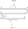
Fig. 5] Fig. 5 is a side view, illustrating an example of the connection relationship between a connector substrate, an intermediate substrate, and an imaging substrate. - There has been a demand for imaging apparatuses that ensure both ease of assembly and sealing performance. An imaging apparatus and a mobile object according to an embodiment of the present disclosure can ensure both ease of assembly and sealing performance.
- Referring to
Figs. 1 to 5 , an imaging apparatus 1 according to an embodiment includes alens 58, aholding member 56, animaging substrate 10, aconnector substrate 20, and ahousing 50. The imaging apparatus 1 may also include afirst sheet metal 30. Thefirst sheet metal 30 is also referred to as a sheet-metal member. - The
housing 50 has an internal space in which thelens 58, theholding member 56, theimaging substrate 10, theconnector substrate 20, and thefirst sheet metal 30 are placed. The internal space of thehousing 50 is defined by aninner wall surface 51 as illustrated inFigs. 1 and2 . Thehousing 50 may be made of a material such as resin. Thehousing 50 may be made of resin or may be made of various materials. - The imaging apparatus 1 captures, by an
imaging device 12 mounted on theimaging substrate 10, an object image formed by thelens 58. Theimaging device 12 produces image data upon capturing the object image. Theimaging substrate 10 is connected to theconnector substrate 20 and outputs the image data to theconnector substrate 20. With theconnector substrate 20 being provided, the imaging apparatus 1 is configured to be connectable to anexternal connector 80. The imaging apparatus 1 outputs the image data to an external apparatus through theexternal connector 80. That is, the imaging apparatus 1 outputs the image data to theexternal connector 80. - The
lens 58 is also referred to as an optical member. Thelens 58 forms an object image incident on the imaging apparatus 1. Theholding member 56 holds thelens 58. Thelens 58 is joined to theholding member 56. Two ormore lenses 58, instead of thelens 58, may be included. At least one ofsuch lenses 58 may be replaced with another optical member, such as a mirror. Thelens 58 may be bonded to theholding member 56 with, for example, an adhesive. Thelens 58 may be joined to theholding member 56 via a fitting structure. Thelens 58 may be joined to theholding member 56 by fastening with screws or the like. - As illustrated in
Fig. 2 , theimaging device 12 is mounted on theimaging substrate 10. Theimaging device 12 has an imaging surface. Theimaging substrate 10 is disposed so that the imaging surface of theimaging device 12 is located in an image-forming plane of thelens 58. An object image formed on the imaging surface by thelens 58 is captured by theimaging device 12. Theimaging device 12 may, for example, be a complementary metal oxide semiconductor (CMOS) image sensor or a charge-coupled device (CCD). In addition to theimaging device 12, a circuit for processing data output from theimaging device 12 may be mounted on theimaging substrate 10. Theimaging substrate 10 may, for example, be a printed circuit board. - The
imaging substrate 10 is joined to theholding member 56. Theimaging substrate 10 may be bonded to theholding member 56 with, for example, an adhesive. Theimaging substrate 10 may be joined to theholding member 56 via a fitting structure. Theimaging substrate 10 may be joined to the holdingmember 56 by fastening with screws or the like. - As illustrated in
Figs. 1 and2 , theconnector substrate 20 and thelens 58 are disposed on opposite sides with respect to theimaging substrate 10 therebetween. In other words, theconnector substrate 20 is farther than theimaging substrate 10 when viewed from thelens 58. - As illustrated in
Figs 1 ,2 , and3 , theconnector substrate 20 is supported by thefirst sheet metal 30 on the negative side in the Z-axis direction. Thefirst sheet metal 30 includes abase 36, which extends along theconnector substrate 20. Thefirst sheet metal 30 also includes substrate-supportingportions 38, which protrude from the base 36 toward the positive side in the Z-axis direction. Theconnector substrate 20 is supported on the positive side in the Z-axis direction of the substrate-supportingportions 38. That is, thefirst sheet metal 30 keeps theconnector substrate 20 from shifting toward the negative side in the Z-axis direction. - Referring to
Figs. 1 and3 , thefirst sheet metal 30 includesprotrusions 34, which protrude from aside surface portion 32 to the positive side and the negative side in the X-axis direction. As illustrated inFig. 3 , eachprotrusion 34 includes a restrictedsection 35, which is a surface on the negative side in the Z-axis direction. Thehousing 50 includes a restrictingsection 53, which is a surface on the positive side in the Z-axis direction of a portion protruding from theinner wall surface 51 toward the negative side in the X-axis direction (seeFig. 3 ). The restrictedsections 35 of thefirst sheet metal 30 are in contact with the restrictingsection 53 of thehousing 50 such that thefirst sheet metal 30 is kept from shifting toward the negative side in the Z-axis direction. As mentioned above, thefirst sheet metal 30 includes the substrate-supportingportions 38 to keep theconnector substrate 20 from shifting toward the negative side in the Z-axis direction. It can thus be said that the restrictingsection 53 of thehousing 50 keeps theconnector substrate 20 from shifting toward the negative side in the Z-axis direction. - As illustrated in
Fig. 4 , theside surface portion 32 of thefirst sheet metal 30 may have acutout 35a. Thecutout 35a is provided in theside surface portion 32 such that theside surface portion 32 includes the restrictedsection 35 oriented toward the negative side in the Z-axis direction. In this case, the restrictedsections 35 of thefirst sheet metal 30 are also in contact with the restrictingsection 53 of thehousing 50 such that thefirst sheet metal 30 is kept from shifting toward the negative side in the Z-axis direction. - The
side surface portion 32 of thefirst sheet metal 30 is elastic. Theside surface portion 32 is configured to be capable of shifting away from theinner wall surface 51 of thehousing 50 toward the inner side, with the bending point on the base 36 as a pivot point. Even when theside surface portion 32 includes theprotrusions 34 protruding toward theinner wall surface 51, thefirst sheet metal 30 is more smoothly accommodated in thehousing 50, because theside surface portion 32 shifts away from theinner wall surface 51 toward the inner side. Once thefirst sheet metal 30 is accommodated in thehousing 50, theside surface portion 32 exerts elastic force toward theinner wall surface 51. The elastic force makes thefirst sheet metal 30 less prone to move in the Z-axis direction. - The
housing 50 has anend portion 52, which is located on the positive side in the Z-axis direction. Thehousing 50 has an opening defined by theend portion 52 on the positive side in the Z-axis direction. The internal space of thehousing 50 communicates with the outside of thehousing 50 through the opening. Theconnector substrate 20 is slid into the internal space of thehousing 50 through the opening. Theexternal connector 80 is inserted toward the negative side in the Z-axis direction and connected to theconnector substrate 20 through the opening. When theexternal connector 80 is inserted into the imaging apparatus 1 toward the negative side in the Z-axis direction and connected, theend portion 52 comes into contact with theexternal connector 80. With theend portion 52 being in contact with theexternal connector 80, the internal space of thehousing 50 is sealed. The direction in which theexternal connector 80 is inserted into the imaging apparatus 1 is also referred to as a first direction. - The
connector substrate 20 has a first surface and a second surface that is opposite to the first surface. The first surface is oriented toward the positive side in the Z-axis direction, and the second surface is oriented toward the negative side in the Z-axis direction. Theconnector substrate 20 includes a terminal 22. The terminal 22 is mounted on the first surface of theconnector substrate 20. The terminal 22 is configured to be connectable to aterminal 82 of theexternal connector 80. The terminal 82 of theexternal connector 80 is connected to theterminal 22 of theconnector substrate 20 such that the terminal 82 presses the terminal 22 toward the negative side in the Z-axis direction. With theconnector substrate 20 being kept from shifting toward the negative side in the Z-axis direction by thehousing 50, the terminal 82 is easily connected to the terminal 22. - If the
connector substrate 20 is not kept from shifting toward the negative side in the Z-axis direction, pressing the terminal 82 of theexternal connector 80 against theterminal 22 of theconnector substrate 20 does not ensure connection between theexternal connector 80 and theconnector substrate 20. In this case, theconnector substrate 20 needs to be connected to theexternal connector 80 before being accommodated in thehousing 50; that is, theconnector substrate 20 needs to be accommodated in thehousing 50 after being connected to theexternal connector 80. This connection procedure may be a constraint on the assembly of the imaging apparatus 1. The present embodiment enables connection of theexternal connector 80 to theconnector substrate 20 in a state in which theconnector substrate 20 is accommodated in thehousing 50. As a result, a higher degree of flexibility is achieved in assembling the imaging apparatus 1. - As illustrated in
Fig. 3 , theconnector substrate 20 includes anend portion 24. Theinner wall surface 51 of thehousing 50 is disposed at a predetermined distance or more from theend portion 24 of theconnector substrate 20. Theconnector substrate 20 is thus movable within a predetermined distance range in the X-axis direction and the Y-axis direction. That is, theconnector substrate 20 is movable within the predetermined range in a direction intersecting the Z-axis. As illustrated inFig. 1 , theinner wall surface 51 of thehousing 50 is larger in size than theconnector substrate 20 in plan view in the Z-axis direction. In this case, theconnector substrate 20 is movable within the predetermined range in a direction intersecting the Z-axis, for example, in the X-axis direction or the Y-axis direction. - As illustrated in
Fig. 3 , theside surface portion 32 of thefirst sheet metal 30 is disposed at a predetermined distance or more from theend portion 24 of theconnector substrate 20. Theconnector substrate 20 is thus movable within a predetermined distance range in the X-axis direction and the Y-axis direction in the state in which theconnector substrate 20 is surrounded by theside surface portion 32 of thefirst sheet metal 30 in the X-axis direction and the Y-axis direction. As illustrated inFig. 1 , theside surface portion 32 on the inner side of thefirst sheet metal 30 is smaller in size than theinner wall surface 51 of thehousing 50 and is larger in size than theconnector substrate 20 in plan view in the Z-axis direction. Theconnector substrate 20 is thus movable within the predetermined range in a direction intersecting the Z-axis, for example, in the X-axis direction or the Y-axis direction, in the state in which theconnector substrate 20 is surrounded by theside surface portion 32. - With the
connector substrate 20 being movable within the predetermined range in a direction intersecting the first direction, theterminal 22 of theconnector substrate 20 and theterminal 82 of theexternal connector 80 are easily brought into alignment with each other to enable connection between the terminal 22 and the terminal 82. Ease of assembly of the imaging apparatus 1 is achieved accordingly. - As illustrated in
Figs. 1 and2 , theconnector substrate 20 is surrounded by thefirst sheet metal 30 and aconductive member 84 of theexternal connector 80. The base 36 (seeFig. 3 ) of thefirst sheet metal 30 is disposed so as to cover at least part of the second surface of theconnector substrate 20. Theside surface portion 32 of thefirst sheet metal 30 is disposed so as to cover at least part of theend portion 24 of theconnector substrate 20. Thefirst sheet metal 30 is made of a conductive material such as metal. Thefirst sheet metal 30 is electrically connected to the ground point of the imaging apparatus 1. Thefirst sheet metal 30 includes theside surface portion 32. Theconductive member 84 is in contact with theside surface portion 32 and is electrically connected to the ground point accordingly. Together with theconductive member 84, thefirst sheet metal 30 provides electromagnetic shielding for theconnector substrate 20. - As illustrated in
Fig. 2 , the imaging apparatus 1 may also include asecond sheet metal 40. Thesecond sheet metal 40 covers theimaging substrate 10. Thesecond sheet metal 40 is made of a conductive material such as metal. Thesecond sheet metal 40 is electrically connected to the ground point of the imaging apparatus 1 to provide electromagnetic shielding for theimaging substrate 10. - The imaging apparatus 1 may also include an
intermediate substrate 70. Theintermediate substrate 70 is covered by thesecond sheet metal 40 as well as thefirst sheet metal 30. Thefirst sheet metal 30 and thesecond sheet metal 40 are electrically connected to the ground point of the imaging apparatus 1 to provide electromagnetic shielding for theintermediate substrate 70. - As illustrated in
Fig. 5 , theconnector substrate 20 may be connected to theintermediate substrate 70 with aflexible substrate 60 therebetween. Theconnector substrate 20 may be connected to theintermediate substrate 70 via a rigid-flexible substrate. Theconnector substrate 20 may be connected to theintermediate substrate 70 via a cable, such as a coaxial cable or a flat cable, or via a wiring harness or the like. Theconnector substrate 20 may be connected to theintermediate substrate 70 via probe pins, such as pogo pins, or via contact terminals or the like. That is, theconnector substrate 20 may be connected to theintermediate substrate 70 so as to be movable with respect to theintermediate substrate 70. With theconnector substrate 20 being movable with respect to theintermediate substrate 70, theterminal 22 of theconnector substrate 20 is easily brought into alignment with the terminal 82 of theexternal connector 80 to enable connection between theconnector substrate 20 and theexternal connector 80. As a result, ease of assembly is achieved. - As illustrated in
Fig. 5 , theintermediate substrate 70 is provided with aboard connector 64, and theimaging substrate 10 is provided with aboard connector 62. Theboard connector 62 and theboard connector 64 are joined together to form a connection between theintermediate substrate 70 and theimaging substrate 10. Theimaging substrate 10 restricts movement of theintermediate substrate 70 accordingly. Although movement of theintermediate substrate 70 is restricted, theconnector substrate 20 is movable with respect to theintermediate substrate 70 such that theconnector substrate 20 is movable with respect to theimaging substrate 10. - In a case in which the imaging apparatus 1 does not include the
intermediate substrate 70, theconnector substrate 20 may be connected to theimaging substrate 10 so as to be movable with respect to theimaging substrate 10. For example, theconnector substrate 20 may be connected to theimaging substrate 10 with theflexible substrate 60 therebetween. Theconnector substrate 20 may be connected to theimaging substrate 10 via a rigid-flexible substrate. Theconnector substrate 20 may be connected to theimaging substrate 10 via a cable, such as a coaxial cable or a flat cable, or via a wiring harness or the like. Theconnector substrate 20 may be connected to theimaging substrate 10 via probe pins, such as pogo pins, or via contact terminals or the like. - The imaging apparatus 1 according to the present disclosure may be installed in a mobile object. The mobile object referred to in the present disclosure may be a vehicle, a ship, or an aircraft. Examples of the vehicle referred to in the present disclosure include automobiles and industrial vehicles and may also include rail cars, vehicles for non-industrial use, and fixed-wing aircrafts that run along runways. The vehicles include passenger cars, trucks, buses, two-wheelers, trolley buses, and other vehicles that travel on roads. The industrial vehicles include agricultural vehicles and construction vehicles. The industrial vehicles include forklifts and golf carts but are not limited to these examples. The industrial vehicles for agricultural use include tractors, cultivators, transplanters, binders, combines, and lawn mowers but are not limited to these examples. The industrial vehicles for construction work include bulldozers, scrapers, excavators, crane trucks, dump trucks, and road rollers but are not limited to these examples. The vehicles also include man-powered vehicles. The classification of vehicles is not limited to the above. For example, automobiles may include industrial vehicles that can travel on roads; that is, the same vehicle may be put into different classifications. Examples of the ship referred to in the present disclosure include marine jets, boats, and tankers. Examples of the aircraft referred to in the present disclosure include fixed-wing aircrafts and rotary wing aircrafts.
- The accompanying drawings are schematic representations of an embodiment of the present disclosure. Constituent elements are not drawn to scale, and the dimension ratios thereof are not necessarily fully corresponding to the actual dimension ratios.
- Although an embodiment of the present disclosure has been described above with reference to the accompanying drawings and by way of examples, various alterations or modifications may be made by those skilled in the art. It is to be understood that such alterations and modifications fall within the scope of the present disclosure. For example, functions and the like of each constituent part or each step can be rearranged in any way that involves no logical inconsistency, and constituent parts or steps can be combined into one or divided. While the present disclosure has been described above with a focus on an embodiment in the form of an apparatus, the present disclosure may be embodied in the form of a method that includes steps performed by constituent parts of an apparatus. Furthermore, the present disclosure may be embodied in the form of a method or program executed by a processor included in an apparatus or may be embodied in the form of a recording medium on which a program is recorded. It is to be understood that such embodiments also fall within the scope of the present disclosure.
- The words "first", "second", and so on in the present disclosure are identifiers for distinguishing between constituent elements. With the constituent elements being distinguishable by "first", "second", and so on in the present disclosure, the identifiers assigned to these constituent elements are interchangeable. For example, the identifiers "first" and "second" that are assigned to the respective lenses are interchangeable. The identifiers are to be interchanged all at once. The elements remain distinguishable from each other after interchanges of identifiers. The identifiers may be omitted. Constituent elements from which the identifiers are omitted are distinguished by reference signs. In the present disclosure, the identifiers "first", "second" and so on should not be used for interpretation of the order of the constituent elements or should not be used as grounds for the presence of lower numbered identifiers.
- In the present disclosure, the X-axis, the Y-axis, and the Z-axis are provided for convenience of illustration and are interchangeable. Constituent elements referred to in the present disclosure have been described using the Cartesian coordinate system based on coordinate axes: the X-axis, the Y-axis, and the Z-axis. It is not required that the constituent elements referred to the present disclosure be orthogonal to each other.
-
- 1 imaging apparatus
- 10 imaging substrate
- 12 imaging device
- 20 connector substrate (22: terminal, 24: end portion)
- 30 first sheet metal (32: side surface portion, 34: protrusion, 35: restricted section, 35a: cutout, 36: base, 38: substrate-supporting portion)
- 40 second sheet metal
- 50 housing (51: inner wall surface, 52: end portion, 53: restricting section)
- 56 holding member
- 58 lens
- 60 flexible substrate (62, 64: board connector) 70 intermediate substrate
- 80 external connector (82: terminal, 84: conductive member)
Claims (10)
- An imaging apparatus, comprising:an imaging substrate provided with an imaging device that produces image data;a connector substrate movably connected to the imaging substrate and including a terminal configured to be connectable in a first direction to an external connector to which the image data is output; anda housing in which the imaging substrate and the connector substrate are accommodated, wherein the housing includes a restricting section that restricts a position of the connector substrate in the first direction, andthe connector substrate is configured to be movable within a predetermined range in a direction intersecting the first direction.
- The imaging apparatus according to Claim 1, whereinthe housing has an inner wall surface that defines an internal space in which the imaging substrate and the connector substrate are placed, andthe inner wall surface is larger in size than the connector substrate in plan view in the first direction.
- The imaging apparatus according to Claim 2, further comprising a sheet-metal member, whereinthe connector substrate hasa first surface on which the terminal configured to be connectable to the external connector is mounted, anda second surface that is opposite to the first surface,the sheet-metal member is disposed so as to cover at least part of the second surface of the connector substrate,
andthe restricting section restricts a position of the sheet-metal member in the first direction. - The imaging apparatus according to Claim 3, whereinthe sheet-metal member includes a side surface portion that is disposed so as to cover at least part of an end portion of the connector substrate, andthe side surface portion is elastic and is configured to be displaceable relative to the inner wall surface.
- The imaging apparatus according to Claim 4, wherein
the side surface portion on an inner side of the sheet-metal member is smaller in size than the inner wall surface and is larger in size than the connector substrate in plan view in the first direction. - The imaging apparatus according to Claim 2, whereinthe housing includes an end portion defining an opening from the internal space toward an outside of the housing,
andthe end portion is configured to, when the external connector is connected to the connector substrate, be in contact with the external connector and seal the opening. - The imaging apparatus according to Claim 3, whereinthe housing includes an end portion defining an opening from the internal space toward an outside of the housing,
andthe end portion is configured to, when the external connector is connected to the connector substrate, be in contact with the external connector and seal the opening. - The imaging apparatus according to Claim 4, whereinthe housing includes an end portion defining an opening from the internal space toward an outside of the housing,
andthe end portion is configured to, when the external connector is connected to the connector substrate, be in contact with the external connector and seal the opening. - The imaging apparatus according to Claim 5, whereinthe housing includes an end portion defining an opening from the internal space toward an outside of the housing,
andthe end portion is configured to, when the external connector is connected to the connector substrate, be in contact with the external connector and seal the opening. - A mobile object in whichan imaging apparatus is installed, the imaging apparatus comprisingan imaging substrate provided with an imaging device that produces image data,a connector substrate movably connected to the imaging substrate and including a terminal configured to be connectable in a first direction to an external connector to which the image data is output; anda housing in which the imaging substrate and the connector substrate are accommodated, wherein the housing includes a restricting section that restricts a position of the connector substrate in the first direction, andthe connector substrate is configured to be movable within a predetermined range in a direction intersecting the first direction.
Applications Claiming Priority (2)
| Application Number | Priority Date | Filing Date | Title |
|---|---|---|---|
| JP2019176166A JP7449666B2 (en) | 2019-09-26 | 2019-09-26 | Imaging device and moving object |
| PCT/JP2020/033938 WO2021059964A1 (en) | 2019-09-26 | 2020-09-08 | Imaging device and moving body |
Publications (3)
| Publication Number | Publication Date |
|---|---|
| EP4037302A1 true EP4037302A1 (en) | 2022-08-03 |
| EP4037302A4 EP4037302A4 (en) | 2023-08-30 |
| EP4037302B1 EP4037302B1 (en) | 2025-04-23 |
Family
ID=75165716
Family Applications (1)
| Application Number | Title | Priority Date | Filing Date |
|---|---|---|---|
| EP20870200.1A Active EP4037302B1 (en) | 2019-09-26 | 2020-09-08 | Imaging device and moving body |
Country Status (5)
| Country | Link |
|---|---|
| US (1) | US12028591B2 (en) |
| EP (1) | EP4037302B1 (en) |
| JP (1) | JP7449666B2 (en) |
| CN (1) | CN114450930B (en) |
| WO (1) | WO2021059964A1 (en) |
Families Citing this family (2)
| Publication number | Priority date | Publication date | Assignee | Title |
|---|---|---|---|---|
| KR20230020242A (en) * | 2021-08-03 | 2023-02-10 | 엘지이노텍 주식회사 | Camera module |
| JP2026068633A (en) * | 2024-10-10 | 2026-04-22 | 京セラ株式会社 | Imaging device |
Family Cites Families (7)
| Publication number | Priority date | Publication date | Assignee | Title |
|---|---|---|---|---|
| JP2002231375A (en) * | 2001-01-30 | 2002-08-16 | Yazaki Corp | Auxiliary module sealing structure |
| CN102326382B (en) * | 2010-03-10 | 2016-04-13 | Smk株式会社 | camera module |
| JP5187328B2 (en) * | 2010-03-12 | 2013-04-24 | オムロン株式会社 | Imaging device for measurement processing |
| JP5565117B2 (en) * | 2010-06-07 | 2014-08-06 | 株式会社リコー | Imaging device |
| JPWO2012104929A1 (en) * | 2011-01-31 | 2014-07-03 | パナソニック株式会社 | Imaging device |
| JP2018085614A (en) * | 2016-11-23 | 2018-05-31 | 日本電産コパル株式会社 | Imaging device |
| JP6827341B2 (en) * | 2017-02-23 | 2021-02-10 | リズム株式会社 | Information processing equipment, cameras and camera equipment |
-
2019
- 2019-09-26 JP JP2019176166A patent/JP7449666B2/en active Active
-
2020
- 2020-09-08 CN CN202080067688.9A patent/CN114450930B/en active Active
- 2020-09-08 WO PCT/JP2020/033938 patent/WO2021059964A1/en not_active Ceased
- 2020-09-08 EP EP20870200.1A patent/EP4037302B1/en active Active
- 2020-09-08 US US17/754,044 patent/US12028591B2/en active Active
Also Published As
| Publication number | Publication date |
|---|---|
| CN114450930A (en) | 2022-05-06 |
| JP7449666B2 (en) | 2024-03-14 |
| CN114450930B (en) | 2024-08-20 |
| US20220385790A1 (en) | 2022-12-01 |
| WO2021059964A1 (en) | 2021-04-01 |
| JP2021057629A (en) | 2021-04-08 |
| US12028591B2 (en) | 2024-07-02 |
| EP4037302A4 (en) | 2023-08-30 |
| EP4037302B1 (en) | 2025-04-23 |
Similar Documents
| Publication | Publication Date | Title |
|---|---|---|
| EP3430797B1 (en) | Camera assembly with shielded imager circuit | |
| EP4037301B1 (en) | Imaging device and mobile body | |
| CN113615153B (en) | Electronic device, imaging device, and moving object | |
| US12028591B2 (en) | Imaging apparatus and mobile object | |
| EP3961300B1 (en) | Electronic instrument, imaging device, and mobile body | |
| JP2019134235A (en) | Fixing structure, imaging device, and movable body | |
| EP3944606B1 (en) | Electronic instrument, image capture device, and mobile body | |
| EP3817356A1 (en) | Bonded structure, imaging device, and moving body | |
| US20260036807A1 (en) | Vehicular camera |
Legal Events
| Date | Code | Title | Description |
|---|---|---|---|
| STAA | Information on the status of an ep patent application or granted ep patent |
Free format text: STATUS: THE INTERNATIONAL PUBLICATION HAS BEEN MADE |
|
| PUAI | Public reference made under article 153(3) epc to a published international application that has entered the european phase |
Free format text: ORIGINAL CODE: 0009012 |
|
| STAA | Information on the status of an ep patent application or granted ep patent |
Free format text: STATUS: REQUEST FOR EXAMINATION WAS MADE |
|
| 17P | Request for examination filed |
Effective date: 20220322 |
|
| AK | Designated contracting states |
Kind code of ref document: A1 Designated state(s): AL AT BE BG CH CY CZ DE DK EE ES FI FR GB GR HR HU IE IS IT LI LT LU LV MC MK MT NL NO PL PT RO RS SE SI SK SM TR |
|
| DAV | Request for validation of the european patent (deleted) | ||
| DAX | Request for extension of the european patent (deleted) | ||
| P01 | Opt-out of the competence of the unified patent court (upc) registered |
Effective date: 20230505 |
|
| REG | Reference to a national code |
Ref country code: DE Ref legal event code: R079 Free format text: PREVIOUS MAIN CLASS: H04N0005225000 Ipc: B60R0011020000 Ref country code: DE Ref legal event code: R079 Ref document number: 602020050140 Country of ref document: DE Free format text: PREVIOUS MAIN CLASS: H04N0005225000 Ipc: B60R0011020000 |
|
| A4 | Supplementary search report drawn up and despatched |
Effective date: 20230728 |
|
| RIC1 | Information provided on ipc code assigned before grant |
Ipc: H04N 23/54 20230101ALI20230724BHEP Ipc: H04N 23/51 20230101ALI20230724BHEP Ipc: G03B 30/00 20210101ALI20230724BHEP Ipc: G03B 17/08 20210101ALI20230724BHEP Ipc: H04N 23/52 20230101ALI20230724BHEP Ipc: G03B 37/00 20210101ALI20230724BHEP Ipc: G03B 17/02 20210101ALI20230724BHEP Ipc: G03B 15/00 20210101ALI20230724BHEP Ipc: G02B 7/02 20210101ALI20230724BHEP Ipc: B60R 11/02 20060101AFI20230724BHEP |
|
| GRAP | Despatch of communication of intention to grant a patent |
Free format text: ORIGINAL CODE: EPIDOSNIGR1 |
|
| STAA | Information on the status of an ep patent application or granted ep patent |
Free format text: STATUS: GRANT OF PATENT IS INTENDED |
|
| INTG | Intention to grant announced |
Effective date: 20241115 |
|
| GRAS | Grant fee paid |
Free format text: ORIGINAL CODE: EPIDOSNIGR3 |
|
| GRAA | (expected) grant |
Free format text: ORIGINAL CODE: 0009210 |
|
| STAA | Information on the status of an ep patent application or granted ep patent |
Free format text: STATUS: THE PATENT HAS BEEN GRANTED |
|
| AK | Designated contracting states |
Kind code of ref document: B1 Designated state(s): AL AT BE BG CH CY CZ DE DK EE ES FI FR GB GR HR HU IE IS IT LI LT LU LV MC MK MT NL NO PL PT RO RS SE SI SK SM TR |
|
| REG | Reference to a national code |
Ref country code: GB Ref legal event code: FG4D |
|
| REG | Reference to a national code |
Ref country code: CH Ref legal event code: EP |
|
| REG | Reference to a national code |
Ref country code: DE Ref legal event code: R096 Ref document number: 602020050140 Country of ref document: DE |
|
| REG | Reference to a national code |
Ref country code: IE Ref legal event code: FG4D |
|
| REG | Reference to a national code |
Ref country code: NL Ref legal event code: MP Effective date: 20250423 |
|
| PG25 | Lapsed in a contracting state [announced via postgrant information from national office to epo] |
Ref country code: NL Free format text: LAPSE BECAUSE OF FAILURE TO SUBMIT A TRANSLATION OF THE DESCRIPTION OR TO PAY THE FEE WITHIN THE PRESCRIBED TIME-LIMIT Effective date: 20250423 |
|
| REG | Reference to a national code |
Ref country code: AT Ref legal event code: MK05 Ref document number: 1787486 Country of ref document: AT Kind code of ref document: T Effective date: 20250423 |
|
| PG25 | Lapsed in a contracting state [announced via postgrant information from national office to epo] |
Ref country code: FI Free format text: LAPSE BECAUSE OF FAILURE TO SUBMIT A TRANSLATION OF THE DESCRIPTION OR TO PAY THE FEE WITHIN THE PRESCRIBED TIME-LIMIT Effective date: 20250423 Ref country code: ES Free format text: LAPSE BECAUSE OF FAILURE TO SUBMIT A TRANSLATION OF THE DESCRIPTION OR TO PAY THE FEE WITHIN THE PRESCRIBED TIME-LIMIT Effective date: 20250423 Ref country code: PT Free format text: LAPSE BECAUSE OF FAILURE TO SUBMIT A TRANSLATION OF THE DESCRIPTION OR TO PAY THE FEE WITHIN THE PRESCRIBED TIME-LIMIT Effective date: 20250825 |
|
| PGFP | Annual fee paid to national office [announced via postgrant information from national office to epo] |
Ref country code: DE Payment date: 20250730 Year of fee payment: 6 |
|
| REG | Reference to a national code |
Ref country code: LT Ref legal event code: MG9D |
|
| PG25 | Lapsed in a contracting state [announced via postgrant information from national office to epo] |
Ref country code: GR Free format text: LAPSE BECAUSE OF FAILURE TO SUBMIT A TRANSLATION OF THE DESCRIPTION OR TO PAY THE FEE WITHIN THE PRESCRIBED TIME-LIMIT Effective date: 20250724 Ref country code: NO Free format text: LAPSE BECAUSE OF FAILURE TO SUBMIT A TRANSLATION OF THE DESCRIPTION OR TO PAY THE FEE WITHIN THE PRESCRIBED TIME-LIMIT Effective date: 20250723 |
|
| PG25 | Lapsed in a contracting state [announced via postgrant information from national office to epo] |
Ref country code: PL Free format text: LAPSE BECAUSE OF FAILURE TO SUBMIT A TRANSLATION OF THE DESCRIPTION OR TO PAY THE FEE WITHIN THE PRESCRIBED TIME-LIMIT Effective date: 20250423 |
|
| PG25 | Lapsed in a contracting state [announced via postgrant information from national office to epo] |
Ref country code: BG Free format text: LAPSE BECAUSE OF FAILURE TO SUBMIT A TRANSLATION OF THE DESCRIPTION OR TO PAY THE FEE WITHIN THE PRESCRIBED TIME-LIMIT Effective date: 20250423 |
|
| PGFP | Annual fee paid to national office [announced via postgrant information from national office to epo] |
Ref country code: GB Payment date: 20250731 Year of fee payment: 6 |
|
| PG25 | Lapsed in a contracting state [announced via postgrant information from national office to epo] |
Ref country code: HR Free format text: LAPSE BECAUSE OF FAILURE TO SUBMIT A TRANSLATION OF THE DESCRIPTION OR TO PAY THE FEE WITHIN THE PRESCRIBED TIME-LIMIT Effective date: 20250423 |
|
| PG25 | Lapsed in a contracting state [announced via postgrant information from national office to epo] |
Ref country code: AT Free format text: LAPSE BECAUSE OF FAILURE TO SUBMIT A TRANSLATION OF THE DESCRIPTION OR TO PAY THE FEE WITHIN THE PRESCRIBED TIME-LIMIT Effective date: 20250423 |
|
| PGFP | Annual fee paid to national office [announced via postgrant information from national office to epo] |
Ref country code: FR Payment date: 20250808 Year of fee payment: 6 |
|
| PG25 | Lapsed in a contracting state [announced via postgrant information from national office to epo] |
Ref country code: RS Free format text: LAPSE BECAUSE OF FAILURE TO SUBMIT A TRANSLATION OF THE DESCRIPTION OR TO PAY THE FEE WITHIN THE PRESCRIBED TIME-LIMIT Effective date: 20250723 |
|
| PG25 | Lapsed in a contracting state [announced via postgrant information from national office to epo] |
Ref country code: IS Free format text: LAPSE BECAUSE OF FAILURE TO SUBMIT A TRANSLATION OF THE DESCRIPTION OR TO PAY THE FEE WITHIN THE PRESCRIBED TIME-LIMIT Effective date: 20250823 |
|
| PG25 | Lapsed in a contracting state [announced via postgrant information from national office to epo] |
Ref country code: LV Free format text: LAPSE BECAUSE OF FAILURE TO SUBMIT A TRANSLATION OF THE DESCRIPTION OR TO PAY THE FEE WITHIN THE PRESCRIBED TIME-LIMIT Effective date: 20250423 |
|
| PG25 | Lapsed in a contracting state [announced via postgrant information from national office to epo] |
Ref country code: SM Free format text: LAPSE BECAUSE OF FAILURE TO SUBMIT A TRANSLATION OF THE DESCRIPTION OR TO PAY THE FEE WITHIN THE PRESCRIBED TIME-LIMIT Effective date: 20250423 Ref country code: DK Free format text: LAPSE BECAUSE OF FAILURE TO SUBMIT A TRANSLATION OF THE DESCRIPTION OR TO PAY THE FEE WITHIN THE PRESCRIBED TIME-LIMIT Effective date: 20250423 |
|
| PG25 | Lapsed in a contracting state [announced via postgrant information from national office to epo] |
Ref country code: CZ Free format text: LAPSE BECAUSE OF FAILURE TO SUBMIT A TRANSLATION OF THE DESCRIPTION OR TO PAY THE FEE WITHIN THE PRESCRIBED TIME-LIMIT Effective date: 20250423 |
|
| PG25 | Lapsed in a contracting state [announced via postgrant information from national office to epo] |
Ref country code: EE Free format text: LAPSE BECAUSE OF FAILURE TO SUBMIT A TRANSLATION OF THE DESCRIPTION OR TO PAY THE FEE WITHIN THE PRESCRIBED TIME-LIMIT Effective date: 20250423 |
|
| REG | Reference to a national code |
Ref country code: DE Ref legal event code: R097 Ref document number: 602020050140 Country of ref document: DE |
|
| PG25 | Lapsed in a contracting state [announced via postgrant information from national office to epo] |
Ref country code: SK Free format text: LAPSE BECAUSE OF FAILURE TO SUBMIT A TRANSLATION OF THE DESCRIPTION OR TO PAY THE FEE WITHIN THE PRESCRIBED TIME-LIMIT Effective date: 20250423 |
|
| PG25 | Lapsed in a contracting state [announced via postgrant information from national office to epo] |
Ref country code: IT Free format text: LAPSE BECAUSE OF FAILURE TO SUBMIT A TRANSLATION OF THE DESCRIPTION OR TO PAY THE FEE WITHIN THE PRESCRIBED TIME-LIMIT Effective date: 20250423 |
|
| PG25 | Lapsed in a contracting state [announced via postgrant information from national office to epo] |
Ref country code: RO Free format text: LAPSE BECAUSE OF FAILURE TO SUBMIT A TRANSLATION OF THE DESCRIPTION OR TO PAY THE FEE WITHIN THE PRESCRIBED TIME-LIMIT Effective date: 20250423 |
|
| PLBE | No opposition filed within time limit |
Free format text: ORIGINAL CODE: 0009261 |
|
| STAA | Information on the status of an ep patent application or granted ep patent |
Free format text: STATUS: NO OPPOSITION FILED WITHIN TIME LIMIT |
|
| REG | Reference to a national code |
Ref country code: CH Ref legal event code: L10 Free format text: ST27 STATUS EVENT CODE: U-0-0-L10-L00 (AS PROVIDED BY THE NATIONAL OFFICE) Effective date: 20260304 |
|
| 26N | No opposition filed |
Effective date: 20260126 |