EP4037185A1 - Level shifter - Google Patents
Level shifter Download PDFInfo
- Publication number
- EP4037185A1 EP4037185A1 EP22152056.2A EP22152056A EP4037185A1 EP 4037185 A1 EP4037185 A1 EP 4037185A1 EP 22152056 A EP22152056 A EP 22152056A EP 4037185 A1 EP4037185 A1 EP 4037185A1
- Authority
- EP
- European Patent Office
- Prior art keywords
- voltage
- receive
- voltages
- pull
- transistor
- Prior art date
- Legal status (The legal status is an assumption and is not a legal conclusion. Google has not performed a legal analysis and makes no representation as to the accuracy of the status listed.)
- Pending
Links
Images


Classifications
-
- H—ELECTRICITY
- H03—ELECTRONIC CIRCUITRY
- H03K—PULSE TECHNIQUE
- H03K3/00—Circuits for generating electric pulses; Monostable, bistable or multistable circuits
- H03K3/02—Generators characterised by the type of circuit or by the means used for producing pulses
- H03K3/353—Generators characterised by the type of circuit or by the means used for producing pulses by the use, as active elements, of field-effect transistors with internal or external positive feedback
- H03K3/356—Bistable circuits
- H03K3/356104—Bistable circuits using complementary field-effect transistors
- H03K3/356182—Bistable circuits using complementary field-effect transistors with additional means for controlling the main nodes
-
- H—ELECTRICITY
- H03—ELECTRONIC CIRCUITRY
- H03K—PULSE TECHNIQUE
- H03K3/00—Circuits for generating electric pulses; Monostable, bistable or multistable circuits
- H03K3/02—Generators characterised by the type of circuit or by the means used for producing pulses
- H03K3/353—Generators characterised by the type of circuit or by the means used for producing pulses by the use, as active elements, of field-effect transistors with internal or external positive feedback
- H03K3/356—Bistable circuits
- H03K3/356104—Bistable circuits using complementary field-effect transistors
- H03K3/356113—Bistable circuits using complementary field-effect transistors using additional transistors in the input circuit
-
- H—ELECTRICITY
- H03—ELECTRONIC CIRCUITRY
- H03K—PULSE TECHNIQUE
- H03K19/00—Logic circuits, i.e. having at least two inputs acting on one output; Inverting circuits
- H03K19/0175—Coupling arrangements; Interface arrangements
- H03K19/0185—Coupling arrangements; Interface arrangements using field effect transistors only
- H03K19/018507—Interface arrangements
-
- H—ELECTRICITY
- H03—ELECTRONIC CIRCUITRY
- H03K—PULSE TECHNIQUE
- H03K17/00—Electronic switching or gating, i.e. not by contact-making and –breaking
- H03K17/10—Modifications for increasing the maximum permissible switched voltage
- H03K17/102—Modifications for increasing the maximum permissible switched voltage in field-effect transistor switches
-
- H—ELECTRICITY
- H03—ELECTRONIC CIRCUITRY
- H03K—PULSE TECHNIQUE
- H03K19/00—Logic circuits, i.e. having at least two inputs acting on one output; Inverting circuits
- H03K19/003—Modifications for increasing the reliability for protection
- H03K19/00315—Modifications for increasing the reliability for protection in field-effect transistor circuits
-
- H—ELECTRICITY
- H03—ELECTRONIC CIRCUITRY
- H03K—PULSE TECHNIQUE
- H03K19/00—Logic circuits, i.e. having at least two inputs acting on one output; Inverting circuits
- H03K19/0175—Coupling arrangements; Interface arrangements
- H03K19/0185—Coupling arrangements; Interface arrangements using field effect transistors only
- H03K19/018507—Interface arrangements
- H03K19/018521—Interface arrangements of complementary type, e.g. CMOS
-
- H—ELECTRICITY
- H03—ELECTRONIC CIRCUITRY
- H03K—PULSE TECHNIQUE
- H03K3/00—Circuits for generating electric pulses; Monostable, bistable or multistable circuits
- H03K3/02—Generators characterised by the type of circuit or by the means used for producing pulses
- H03K3/353—Generators characterised by the type of circuit or by the means used for producing pulses by the use, as active elements, of field-effect transistors with internal or external positive feedback
- H03K3/356—Bistable circuits
- H03K3/356104—Bistable circuits using complementary field-effect transistors
- H03K3/356113—Bistable circuits using complementary field-effect transistors using additional transistors in the input circuit
- H03K3/35613—Bistable circuits using complementary field-effect transistors using additional transistors in the input circuit the input circuit having a differential configuration
Definitions
- the present disclosure relates generally to electronic circuits, and, more particularly, to a level shifter.
- SoC system-on-chip
- a level shifter is used as an interface between the components to shift voltage levels of input voltages associated with one voltage domain to voltage levels of output voltages associated with another voltage domain.
- a conventional level shifter includes pull-up and pull-down circuits and a voltage protection circuit.
- the voltage protection circuit protects gate-to-source and drain-to-source voltages of transistors of the pull-up and pull-down circuits from reaching high voltages that may damage the transistors.
- the output voltages generated by the conventional level shifter are unable to reach minimum and maximum voltage levels of the other voltage domain.
- the output voltages vary due to variations in process, voltage, and temperature (PVT) associated with the conventional level shifter.
- PVT process, voltage, and temperature
- large-sized transistors are implemented in the voltage protection circuit. Inclusion of such large-sized transistors results in an increase in a size of the conventional level shifter and a degradation in a speed of operation of the conventional level shifter. Therefore, there exists a need for a level shifter that solves the aforementioned problems of the conventional level shifter.
- a level shifter comprises a pull-down circuit, a pull-up circuit, a protection circuit, and an output generator.
- the pull-down circuit is configured to receive first and second input voltages, and generate first and second bias voltages.
- the first and second input voltages are associated with a first voltage domain.
- the pull-up circuit is configured to receive a supply voltage and generate first and second control voltages.
- the protection circuit is coupled between the pull-down circuit and the pull-up circuit, and configured to receive first and second reference voltages, and control the generation of the first and second bias voltages and the first and second control voltages.
- the output generator is coupled with the pull-down circuit and the protection circuit, and configured to receive the second reference voltage and the first and second bias voltages, and generate first and second output voltages.
- the first and second output voltages are associated with a second voltage domain.
- a level shifter in another embodiment, comprises a pull-down circuit, a pull-up circuit, a protection circuit, and an output generator.
- the pull-down circuit is configured to receive first and second input voltages, and generate first and second bias voltages.
- the first and second input voltages are associated with a first voltage domain.
- the pull-up circuit is configured to receive a supply voltage and generate first and second control voltages.
- the protection circuit is coupled between the pull-down circuit and the pull-up circuit, and configured to receive first and second reference voltages, and control the generation of the first and second bias voltages and the first and second control voltages.
- the output generator is coupled with the pull-down circuit, the pull-up circuit, and the protection circuit, and configured to receive the first and second reference voltages, the first and second bias voltages, and the first and second control voltages, and generate first through fourth output voltages.
- the first and second output voltages are associated with a second voltage domain
- the third and fourth output voltages are associated with a third voltage domain.
- a system-on-chip includes a core and a level shifter that is coupled with the core.
- the core is configured to receive a first supply voltage and generate first and second input voltages.
- the first and second input voltages are associated with a first voltage domain.
- the level shifter comprises a pull-down circuit, a pull-up circuit, a protection circuit, and an output generator.
- the pull-down circuit is configured to receive the first and second input voltages, and generate first and second bias voltages.
- the pull-up circuit is configured to receive a second supply voltage and generate first and second control voltages.
- the protection circuit is coupled between the pull-down circuit and the pull-up circuit, and configured to receive first and second reference voltages, and control the generation of the first and second bias voltages and the first and second control voltages.
- the output generator is coupled with the pull-up circuit, the pull-down circuit, and the protection circuit, and configured to receive the first and second bias voltages and one of (i) the second reference voltage and (ii) the first and second reference voltages and the first and second control voltages, and generate a plurality of output voltages.
- the plurality of output voltages are associated with at least one of second and third voltage domains.
- the pull-down circuit includes first and second transistors.
- the first transistor has a gate terminal configured to receive the first input voltage, a source terminal coupled with a ground terminal, and a drain terminal configured to generate the first bias voltage.
- the second transistor has a gate terminal configured to receive the second input voltage, a source terminal coupled with the ground terminal, and a drain terminal configured to generate the second bias voltage.
- the pull-up circuit includes first and second transistors.
- the first transistor has a gate terminal configured to receive the second control voltage, a source terminal configured to receive the supply voltage, and a drain terminal configured to generate the first control voltage.
- the second transistor has a gate terminal coupled with the drain terminal of the first transistor, and configured to receive the first control voltage.
- the second transistor further has a source terminal configured to receive the supply voltage, and a drain terminal coupled with the gate terminal of the first transistor, and configured to generate and provide the second control voltage to the gate terminal of the first transistor.
- the protection circuit includes first through fourth transistors.
- the first transistor has a gate terminal configured to receive the first reference voltage, and a source terminal coupled with the pull-up circuit, and configured to control the generation of the first control voltage.
- the second transistor has a gate terminal configured to receive the first reference voltage, and a source terminal coupled with the pull-up circuit, and configured to control the generation of the second control voltage.
- the third transistor has a gate terminal configured to receive the second reference voltage, and a source terminal coupled with the pull-down circuit, and configured to control the generation of the first bias voltage.
- the third transistor further has a drain terminal coupled with a drain terminal of the first transistor.
- the fourth transistor has a gate terminal configured to receive the second reference voltage, and a source terminal coupled with the pull-down circuit, and configured to control the generation of the second bias voltage.
- the fourth transistor further has a drain terminal coupled with a drain terminal of the second transistor.
- the output generator includes first and second transistors.
- the first transistor has a gate terminal coupled with the pull-down circuit and the protection circuit, and configured to receive the second bias voltage.
- the first transistor further has a source terminal configured to receive the second reference voltage, and a drain terminal configured to generate the first output voltage.
- the second transistor has a gate terminal coupled with the drain terminal of the first transistor, the pull-down circuit, and the protection circuit, and configured to receive the first bias voltage.
- the second transistor further has a source terminal configured to receive the second reference voltage, and a drain terminal coupled with the gate terminal of the first transistor, and configured to generate the second output voltage.
- the level shifter further comprises a voltage divider network that is coupled with the protection circuit and the output generator.
- the voltage divider is configured to receive the supply voltage, generate the first and second reference voltages, and provide the first and second reference voltages to the protection circuit, and the second reference voltage to the output generator.
- the voltage divider network includes first through third resistors coupled in series.
- the first resistor is configured to receive the supply voltage, and the third resistor is coupled with a ground terminal.
- the first and second reference voltages are generated based on a voltage drop across each of the first through third resistors.
- the level shifter further comprises a resistor and a capacitor.
- the resistor is coupled with the voltage divider network, and configured to receive the second reference voltage.
- the capacitor is coupled with the resistor and a ground terminal, and configured to charge to the second reference voltage.
- the level shifter comprises a pull-down circuit, a pull-up circuit, a protection circuit, and an output generator.
- the pull-down circuit is configured to receive input voltages, and generate bias voltages. The input voltages are associated with a voltage domain.
- the pull-up circuit is configured to receive a supply voltage and generate control voltages.
- the protection circuit is configured to receive reference voltages, and control the generation of the bias voltages and the control voltages.
- the output generator is configured to receive the bias voltages and one of the reference voltages, and generate output voltages. The output voltages are associated with another voltage domain.
- the output voltages are generated by the output generator such that the output voltages are able to reach minimum and maximum voltage levels of the other voltage domain, and the output voltages do not vary due to variations in process, voltage, and temperature (PVT) associated with the level shifter. Additionally, a need to utilize large-sized transistors in the protection circuit is eliminated. Thus, a size of the level shifter is reduced and a speed of operation of the level shifter is increased as compared to conventional level shifters that utilize large-sized transistors in a protection circuit of the conventional level shifters.
- FIG. 1 is a schematic block diagram of a system-on-chip (SoC) 100 in accordance with an embodiment of the present disclosure.
- SoC system-on-chip
- the SoC 100 may be utilized in applications that require different components of the SoC 100 to operate in different voltage domains.
- the SoC 100 includes a core 102, a first level shifter 104, and a first processing circuit 106.
- the core 102 is a processing element of the SoC 100, and configured to receive a first supply voltage VDDA and generate first and second input voltages VII and VI2.
- a first supply generator (not shown) is coupled with the core 102, and configured to generate and provide the first supply voltage VDDA to the core 102.
- the first supply generator may be included on the SoC 100.
- the core 102 is further configured to operate at the first supply voltage VDDA.
- the first and second input voltages VII and VI2 are associated with a first voltage domain.
- the first voltage domain corresponds to voltages in the range of '0 - 0.75' volts.
- Examples of the core 102 include, but are not limited to, a microprocessor core and a microcontroller core.
- the first level shifter 104 is coupled with the core 102, and configured to receive a second supply voltage VDDB and the first and second input voltages VII and VI2, and shift voltage levels of the first and second input voltages VII and VI2 to generate first and second output voltages VO1 and VO2.
- a second supply generator (not shown) is coupled with the first level shifter 104, and configured to generate and provide the second supply voltage VDDB to the first level shifter 104.
- the second supply generator may be included on the SoC 100.
- the first level shifter 104 is further configured to operate at the second supply voltage VDDB. In one example, the second supply voltage VDDB is '1.8' volts.
- the first and second output voltages VO1 and VO2 are associated with a second voltage domain.
- the second voltage domain corresponds to voltages in the range of '0 - 1.65' volts.
- the first level shifter 104 has been explained in detail in FIG. 2 .
- the first processing circuit 106 is coupled with the first level shifter 104, and configured to receive the first and second output voltages VO1 and VO2.
- the first processing circuit 106 is further coupled with the second supply generator, and further configured to receive the second supply voltage VDDB.
- the first processing circuit 106 includes a switching transistor (not shown) such that a gate terminal of the switching transistor is configured to receive one of the first and second output voltages VO1 and VO2 for controlling a switching operation of the switching transistor.
- FIG. 2 is a schematic block diagram of the first level shifter 104 in accordance with an embodiment of the present disclosure.
- the first level shifter 104 includes a voltage divider network 202 that includes first through third resistors R1-R3 coupled in series, a fourth resistor R4, a first capacitor C1, a pull-up circuit 204, a protection circuit 206, a pull-down circuit 208, and a first output generator 210.
- the voltage divider network 202 is coupled with the second supply generator, and configured to receive the second supply voltage VDDB and generate first and second reference voltages VR1 and VR2.
- the first resistor R1 is configured to receive the second supply voltage VDDB whereas the third resistor R3 is coupled with a ground terminal.
- the second resistor R2 is coupled between the first and third resistors R1 and R3.
- the first and second reference voltages VR1 and VR2 are generated based on a voltage drop across each of the first through third resistors R1-R3.
- the first reference voltage VR1 is generated between the second and third resistors R2 and R3, and the second reference voltage VR2 is generated between the first and second resistors R1 and R2.
- the voltage divider network 202 is further coupled with the protection circuit 206 and the first output generator 210, and further configured to provide the first and second reference voltages VR1 and VR2 to the protection circuit 206, and the second reference voltage VR2 to the first output generator 210.
- the fourth resistor R4 is coupled with the voltage divider network 202, and configured to receive the second reference voltage VR2.
- the first capacitor C1 is coupled with the fourth resistor R4 and the ground terminal, and configured to charge to the second reference voltage VR2.
- the fourth resistor R4 and the first capacitor C1 are utilized to prevent back coupling of the first and second output voltages VO1 and VO2 due to transitions in the first and second output voltages VO1 and VO2.
- the pull-up circuit 204 is configured to receive the second supply voltage VDDB and generate first and second control voltages VC1 and VC2.
- the pull-up circuit 204 includes first and second transistors T1 and T2.
- the first transistor T1 has a source terminal that is coupled with the second supply generator, and configured to receive the second supply voltage VDDB.
- the first transistor T1 further has a gate terminal that is configured to receive the second control voltage VC2, and a drain terminal that is configured to generate the first control voltage VC1.
- the first control voltage VC1 is thus generated based on the second supply voltage VDDB and the second control voltage VC2.
- the second transistor T2 has a gate terminal that is coupled with the drain terminal of the first transistor T1, and configured to receive the first control voltage VC1.
- the second transistor T2 further has a source terminal that is coupled with the second supply generator, and a drain terminal that is coupled with the gate terminal of the first transistor T1.
- the source terminal of the second transistor T2 is configured to receive the second supply voltage VDDB
- the drain terminal of the second transistor T2 is configured to generate and provide the second control voltage VC2 to the gate terminal of the first transistor T1.
- the second control voltage VC2 is thus generated based on the second supply voltage VDDB and the first control voltage VC1.
- the first and second transistors T1 and T2 are p-channel metal oxide semiconductor (PMOS) transistors.
- the pull-down circuit 208 is coupled with the core 102, and configured to receive the first and second input voltages VII and VI2, and generate first and second bias voltages VB1 and VB2.
- the pull-down circuit 208 includes third and fourth transistors T3 and T4.
- the third transistor T3 has a gate terminal that is coupled with the core 102, and a source terminal coupled with a ground terminal.
- the gate terminal of the third transistor T3 is configured to receive the first input voltage VII.
- the third transistor T3 further has a drain terminal that is configured to generate the first bias voltage VB1.
- the fourth transistor T4 has a gate terminal that is coupled with the core 102, and a source terminal that is coupled with the ground terminal.
- the gate terminal of the fourth transistor T4 is configured to receive the second input voltage VI2.
- the fourth transistor T4 further has a drain terminal that is configured to generate the second bias voltage VB2.
- the third and fourth transistors T3 and T4 are n-channel metal oxide semiconductor (NMOS) transistors.
- the protection circuit 206 is coupled with the voltage divider network 202, the fourth resistor R4, and the first capacitor C1, and configured to receive the first and second reference voltages VR1 and VR2.
- the protection circuit 206 is further coupled between the pull-down circuit 208 and the pull-up circuit 204, and further configured to control the generation of the first and second bias voltages VB1 and VB2 and the first and second control voltages VC1 and VC2.
- the protection circuit 206 includes fifth through eighth transistors T5-T8.
- the fifth transistor T5 has a gate terminal that is coupled with the second and third resistors R2 and R3, and configured to receive the first reference voltage VR1.
- the fifth transistor T5 further has a source terminal that is coupled with the pull-up circuit 204 (i.e., the drain terminal of the first transistor T1), and configured to control the generation of the first control voltage VC1. Based on the first reference voltage VR1 received at the gate terminal of the fifth transistor T5, the first control voltage VC1 flows from the source terminal of the fifth transistor T5 to a drain terminal of the fifth transistor T5.
- the pull-up circuit 204 i.e., the drain terminal of the first transistor T1
- the sixth transistor T6 has a gate terminal that is coupled with the second and third resistors R2 and R3, and configured to receive the first reference voltage VR1.
- the sixth transistor T6 further has a source terminal that is coupled with the pull-up circuit 204 (i.e., the drain terminal of the second transistor T2), and configured to control the generation of the second control voltage VC2. Based on the first reference voltage VR1 received at the gate terminal of the sixth transistor T6, the second control voltage VC2 flows from the source terminal of the sixth transistor T6 to a drain terminal of the sixth transistor T6.
- the fifth transistor T5 controls the generation of the first control voltage VC1 such that the first control voltage VC1 is '0.35 + Vt' volts, where 'Vt' is a threshold voltage associated with the fifth transistor T5.
- the second transistor T2 receives the first control voltage VC1 at the gate terminal thereof and thus a gate-to-source voltage (not shown) of the second transistor T2 is '1.45 - Vt' volts.
- the first transistor T1 receives the second supply voltage VDDB, i.e., '1.8' volts, at the source terminal thereof and thus a drain-to-source voltage (not shown) of the first transistor T1 is '1.45 - Vt' volts.
- the fifth transistor T5 is further configured to protect the drain-to-source voltage and the gate-to-source voltage of the first and second transistors T1 and T2, respectively, from reaching a high voltage, i.e., '1.8' volts, that may damage the first and second transistors T1 and T2.
- the sixth transistor T6 is further configured to protect a gate-to-source voltage and a drain-to-source voltage of the first and second transistors T1 and T2, respectively, from reaching the high voltage of 1.8 volts.
- the fifth and sixth transistors T5 and T6 are PMOS transistors.
- the seventh transistor T7 has a gate terminal that is coupled with the fourth resistor R4 and the first capacitor C1, and configured to receive the second reference voltage VR2.
- the seventh transistor T7 further has a source terminal that is coupled with the pull-down circuit 208 (i.e., the drain terminal of the third transistor T3), and a drain terminal that is coupled with the drain terminal of the fifth transistor T5.
- the source terminal of the seventh transistor T7 is configured to control the generation of the first bias voltage VB1. Based on the second reference voltage VR2 received at the gate terminal of the seventh transistor T7, the first bias voltage VB1 flows from the source terminal of the seventh transistor T7 to the drain terminal of the seventh transistor T7.
- the eighth transistor T8 has a gate terminal that is coupled with the fourth resistor R4 and the first capacitor C1, and configured to receive the second reference voltage VR2.
- the eighth transistor T8 further has a source terminal that is coupled with the pull-down circuit 208 (i.e., the drain terminal of the fourth transistor T4), and a drain terminal coupled with the drain terminal of the sixth transistor T6.
- the source terminal of the eighth transistor T8 is configured to control the generation of the second bias voltage VB2. Based on the second reference voltage VR2 received at the gate terminal of the eighth transistor T8, the second bias voltage VB2 flows from the source terminal of the eighth transistor T8 to the drain terminal of the eighth transistor T8.
- the seventh and eighth transistors T7 and T8 are further configured to protect gate-to-source voltages and drain-to-source voltages of the third and fourth transistors T3 and T4 from reaching high voltages that may damage the third and fourth transistors T3 and T4.
- the seventh and eighth transistors T7 and T8 are NMOS transistors.
- the first output generator 210 is coupled with the fourth resistor R4, the first capacitor C1, the pull-down circuit 208, and the protection circuit 206, and configured to receive the second reference voltage VR2 and the first and second bias voltages VB 1 and VB2, and generate the first and second output voltages VO1 and VO2.
- the first output generator 210 includes ninth and tenth transistors T9 and T10.
- the ninth transistor T9 has a gate terminal that is coupled with the pull-down circuit 208 (i.e., the drain terminal of the fourth transistor T4) and the protection circuit 206 (i.e., the source terminal of the eighth transistor T8), and configured to receive the second bias voltage VB2.
- the ninth transistor T9 further has a source terminal that is coupled with the fourth resistor R4 and the first capacitor C1, and configured to receive the second reference voltage VR2.
- the ninth transistor T9 further has a drain terminal that is configured to generate the first output voltage VO1.
- the tenth transistor T10 has a gate terminal that is coupled with the drain terminal of the ninth transistor T9, the pull-down circuit 208 (i.e., the drain terminal of the third transistor T3), and the protection circuit 206 (i.e., the source terminal of the seventh transistor T7), and configured to receive the first bias voltage VB1.
- the tenth transistor T10 further has a source terminal that is coupled with the fourth resistor R4 and the first capacitor C1, and configured to receive the second reference voltage VR2.
- the tenth transistor T10 further has a drain terminal that is coupled with the gate terminal of the ninth transistor T9, and configured to generate the second output voltage VO2.
- the ninth transistor T9 is in a non-conducting state and the tenth transistor T10 is in a conducting state.
- the tenth transistor T10 outputs the second reference voltage VR2 (i.e., '1.65' volts) as the second output voltage VO2
- the ninth transistor T9 outputs the first bias voltage VB1 (i.e., '0' volts) as the first output voltage VO1 such that the first and second output voltages VO1 and VO2 reach minimum and maximum voltage levels (i.e., '0' volts and '1.65' volts, respectively) of the second voltage domain.
- the ninth and tenth transistors T9 and T10 are PMOS transistors.
- FIG. 3 is a schematic block diagram of the SoC 100 in accordance with another embodiment of the present disclosure.
- the SoC 100 includes the core 102, a second level shifter 302, the first processing circuit 106, and a second processing circuit 304.
- the core 102 functions in a similar manner as described in FIG. 1 .
- the second level shifter 302 is coupled with the core 102, and configured to receive the second supply voltage VDDB such that the second level shifter 302 is configured to operate at the second supply voltage VDDB.
- the second level shifter 302 is further configured to receive the first and second input voltages VII and VI2, and shift voltage levels of the first and second input voltages VII and VI2 to generate a plurality of output voltages, i.e., the first and second output voltages VO1 and VO2 and third and fourth output voltages VO3 and VO4.
- the second supply voltage VDDB is '1.8' volts.
- the first and second output voltages VO1 and VO2 are associated with the second voltage domain, and the third and fourth output voltages VO3 and VO4 are associated with a third voltage domain.
- the second voltage domain corresponds to voltages in the range of '0 - 1.65' volts and the third voltage domain corresponds to voltages in the range of '0.35 - 1.8' volts.
- the second level shifter 302 has been explained in detail in FIG. 4 .
- the first processing circuit 106 functions in a similar manner as described in FIG. 1 .
- the second processing circuit 304 is coupled with the second level shifter 302, and configured to receive the third and fourth output voltages VO3 and VO4.
- the second processing circuit 304 is further coupled with the second supply generator, and further configured to receive the second supply voltage VDDB.
- the second processing circuit 304 may be structurally similar to the first processing circuit 106.
- the first and second processing circuits 106 and 304 include transistors (not shown) such that the transistors are controlled based on the first through fourth output voltages VO1-VO4 for executing various operations associated with the SoC 100.
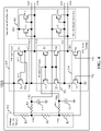
- FIG. 4 is a schematic block diagram of the second level shifter 302 in accordance with another embodiment of the present disclosure.
- the second level shifter 302 includes the voltage divider network 202 that includes the first through third resistors R1-R3 coupled in series, the fourth resistor R4, the first capacitor C1, a fifth resistor R5, a second capacitor C2, the pull-up circuit 204, the protection circuit 206, the pull-down circuit 208, and a second output generator 402.
- the voltage divider network 202 is coupled with the second supply generator, and configured to receive the second supply voltage VDDB and generate the first and second reference voltages VR1 and VR2.
- the voltage divider network 202 is further coupled with the protection circuit 206 and the second output generator 402, and further configured to provide the first and second reference voltages VR1 and VR2 to the protection circuit 206 and the second output generator 402.
- the first through third resistors R1-R3, the fourth resistor R4, and the first capacitor C1 function in a similar manner as described in FIG. 2 .
- the fifth resistor R5 is coupled with the voltage divider network 202, and configured to receive the second reference voltage VR2.
- the second capacitor C2 is coupled with the fifth resistor R5 and the ground terminal, and configured to charge to the first reference voltage VR1.
- the fifth resistor R5 and the second capacitor C2 are utilized to prevent back coupling of the third and fourth output voltages VO3 and VO4 due to transitions in the third and fourth output voltages VO3 and VO4.
- the pull-up circuit 204, the pull-down circuit 208, and the protection circuit 206 function in a similar manner as described in FIG. 2 .
- the second output generator 402 is coupled with the pull-up circuit 204, the pull-down circuit 208, and the protection circuit 206, and configured to receive the first and second reference voltages VR1 and VR2, the first and second bias voltages VB1 and VB2, and the first and second control voltages VC1 and VC2, and generate the first through fourth output voltages VO1-VO4.
- the second output generator 402 includes the ninth and tenth transistors T9 and T10 and eleventh and twelfth transistors T11 and T12. The ninth and tenth transistors T9 and T10 function in a similar manner as described in FIG. 2 .
- the eleventh transistor T11 has a gate terminal that is coupled with the pull-up circuit 204 (i.e., the drain terminal of the second transistor T2) and the protection circuit 206 (i.e., the source terminal of the sixth transistor T6), and configured to receive the second control voltage VC2.
- the eleventh transistor T11 further has a drain terminal that is coupled with the fifth resistor R5 and the second capacitor C2, and configured to receive the first reference voltage VR1, and a source terminal that is configured to output the third output voltage VO3. Based on the second control voltage VC2 received at the gate terminal of the eleventh transistor T11, the first reference voltage VR1 flows from the drain terminal of the eleventh transistor T11 to the source terminal of the eleventh transistor T11.
- the twelfth transistor T12 has a gate terminal that is coupled with the source terminal of the eleventh transistor T11, the pull-up circuit 204 (i.e., the drain terminal of the first transistor T1), and the protection circuit 206 (i.e., the source terminal of the fifth transistor T5), and configured to receive the first control voltage VC1.
- the twelfth transistor T12 further has a drain terminal that is coupled with the fifth resistor R5 and the second capacitor C2, and configured to receive the first reference voltage VR1. Further, the twelfth transistor T12 has a source terminal that is coupled with the gate terminal of the eleventh transistor T11, and configured to output the fourth output voltage VO4.
- the first reference voltage VR1 flows from the drain terminal of the twelfth transistor T12 to the source terminal of the twelfth transistor T12.
- the first control voltage VC1 is '0.35 + Vt' volts and the second control voltage VC2 is '1.8' volts and thus the eleventh transistor T11 is in a conducting state and the twelfth transistor T12 is in a non-conducting state.
- the eleventh transistor T11 outputs the first reference voltage VR1 (i.e., '0.35' volts) as the third output voltage VO3
- the twelfth transistor T12 outputs the second control voltage VC2 (i.e., '1.8' volts) as the fourth output voltage VO4 such that the third and fourth output voltages VO3 and VO4 reach minimum and maximum voltage levels (i.e., '0.35' volts and '1.8' volts, respectively) of the third voltage domain.
- the eleventh and twelfth transistors T11 and T12 are NMOS transistors.
- a third level shifter may be obtained by including a third output generator (not shown) that includes the eleventh and twelfth transistors T11 and T12 in place of the second output generator 402, in the second level shifter 302.
- the third output generator is thus configured to receive the first reference voltage VR1 and the first and second control voltages VC1 and VC2, and generate the third and fourth output voltages VO3 and VO4.
- the working of the third level shifter is similar to the second level shifter 302 and will be understood by a person skilled in the art.
- the first and second output voltages VO1 and VO2 are generated by the first output generator 210 (as explained in FIG. 2 ) and the first through fourth output voltages VO1-VO4 are generated by the second output generator 402 (as explained in FIG. 4 ), the first and second output voltages VO1 and VO2 are able to reach the minimum and maximum voltage levels associated with the second voltage domain whereas the first through fourth output voltages VO1-VO4 are able to reach the minimum and maximum voltage levels associated with one of the second and third voltage domains.
- first through fourth output voltages VO1-VO4 are based on the second and first bias voltages VB2 and VB1 and the second and first control voltages VC2 and VC1 received at the gate terminals of the ninth through twelfth transistors T9-T12, respectively, and the first and second reference voltages VR1 and VR2.
- first through fourth output voltages VO1-VO4 are not directly based on an internal voltage drop associated with the ninth through twelfth transistors T9-T12, respectively, and remain unaffected due to variations in process, voltage, and temperature (PVT) associated with the first and second level shifters 104 and 302.
- the first and second level shifters 104 and 302 operate at a higher speed as compared to the conventional level shifters.
- a level shifter includes a pull-down circuit, a pull-up circuit, a protection circuit, and an output generator.
- the pull-down circuit is configured to receive input voltages, and generate bias voltages. The input voltages are associated with a voltage domain.
- the pull-up circuit is configured to receive a supply voltage and generate control voltages.
- the protection circuit is configured to receive reference voltages, and control the generation of the bias voltages and the control voltages.
- the output generator is configured to receive at least one of the reference voltages, and at least one of the bias voltages and the control voltages, and generate output voltages that are able to reach minimum and maximum voltage levels of another voltage domain. Further, the output voltages remain unaffected by variations in process, voltage, and temperature.
- Coupled is not intended to be limited to a direct coupling or a mechanical coupling.
Landscapes
- Engineering & Computer Science (AREA)
- Computer Hardware Design (AREA)
- Physics & Mathematics (AREA)
- Computing Systems (AREA)
- General Engineering & Computer Science (AREA)
- Mathematical Physics (AREA)
- Logic Circuits (AREA)
Abstract
Description
- The present disclosure relates generally to electronic circuits, and, more particularly, to a level shifter.
- A system-on-chip (SoC) includes multiple components that operate under various voltage domains, i.e., voltages that are in a peculiar range (such as, '0-1.8' volts). A level shifter is used as an interface between the components to shift voltage levels of input voltages associated with one voltage domain to voltage levels of output voltages associated with another voltage domain.
- A conventional level shifter includes pull-up and pull-down circuits and a voltage protection circuit. The voltage protection circuit protects gate-to-source and drain-to-source voltages of transistors of the pull-up and pull-down circuits from reaching high voltages that may damage the transistors. Thus, the output voltages generated by the conventional level shifter are unable to reach minimum and maximum voltage levels of the other voltage domain. Further, the output voltages vary due to variations in process, voltage, and temperature (PVT) associated with the conventional level shifter. To reduce the effects of PVT variations on the output voltages, large-sized transistors are implemented in the voltage protection circuit. Inclusion of such large-sized transistors results in an increase in a size of the conventional level shifter and a degradation in a speed of operation of the conventional level shifter. Therefore, there exists a need for a level shifter that solves the aforementioned problems of the conventional level shifter.
- In one embodiment, a level shifter is disclosed. The level shifter comprises a pull-down circuit, a pull-up circuit, a protection circuit, and an output generator. The pull-down circuit is configured to receive first and second input voltages, and generate first and second bias voltages. The first and second input voltages are associated with a first voltage domain. The pull-up circuit is configured to receive a supply voltage and generate first and second control voltages. The protection circuit is coupled between the pull-down circuit and the pull-up circuit, and configured to receive first and second reference voltages, and control the generation of the first and second bias voltages and the first and second control voltages. The output generator is coupled with the pull-down circuit and the protection circuit, and configured to receive the second reference voltage and the first and second bias voltages, and generate first and second output voltages. The first and second output voltages are associated with a second voltage domain.
- In another embodiment, a level shifter is disclosed. The level shifter comprises a pull-down circuit, a pull-up circuit, a protection circuit, and an output generator. The pull-down circuit is configured to receive first and second input voltages, and generate first and second bias voltages. The first and second input voltages are associated with a first voltage domain. The pull-up circuit is configured to receive a supply voltage and generate first and second control voltages. The protection circuit is coupled between the pull-down circuit and the pull-up circuit, and configured to receive first and second reference voltages, and control the generation of the first and second bias voltages and the first and second control voltages. The output generator is coupled with the pull-down circuit, the pull-up circuit, and the protection circuit, and configured to receive the first and second reference voltages, the first and second bias voltages, and the first and second control voltages, and generate first through fourth output voltages. The first and second output voltages are associated with a second voltage domain, and the third and fourth output voltages are associated with a third voltage domain.
- In yet another embodiment, a system-on-chip (SoC) is disclosed. The SoC includes a core and a level shifter that is coupled with the core. The core is configured to receive a first supply voltage and generate first and second input voltages. The first and second input voltages are associated with a first voltage domain. The level shifter comprises a pull-down circuit, a pull-up circuit, a protection circuit, and an output generator. The pull-down circuit is configured to receive the first and second input voltages, and generate first and second bias voltages. The pull-up circuit is configured to receive a second supply voltage and generate first and second control voltages. The protection circuit is coupled between the pull-down circuit and the pull-up circuit, and configured to receive first and second reference voltages, and control the generation of the first and second bias voltages and the first and second control voltages. The output generator is coupled with the pull-up circuit, the pull-down circuit, and the protection circuit, and configured to receive the first and second bias voltages and one of (i) the second reference voltage and (ii) the first and second reference voltages and the first and second control voltages, and generate a plurality of output voltages. The plurality of output voltages are associated with at least one of second and third voltage domains.
- In some embodiments, the pull-down circuit includes first and second transistors. The first transistor has a gate terminal configured to receive the first input voltage, a source terminal coupled with a ground terminal, and a drain terminal configured to generate the first bias voltage. The second transistor has a gate terminal configured to receive the second input voltage, a source terminal coupled with the ground terminal, and a drain terminal configured to generate the second bias voltage.
- In some embodiments, the pull-up circuit includes first and second transistors. The first transistor has a gate terminal configured to receive the second control voltage, a source terminal configured to receive the supply voltage, and a drain terminal configured to generate the first control voltage. The second transistor has a gate terminal coupled with the drain terminal of the first transistor, and configured to receive the first control voltage. The second transistor further has a source terminal configured to receive the supply voltage, and a drain terminal coupled with the gate terminal of the first transistor, and configured to generate and provide the second control voltage to the gate terminal of the first transistor.
- In some embodiments, the protection circuit includes first through fourth transistors. The first transistor has a gate terminal configured to receive the first reference voltage, and a source terminal coupled with the pull-up circuit, and configured to control the generation of the first control voltage. The second transistor has a gate terminal configured to receive the first reference voltage, and a source terminal coupled with the pull-up circuit, and configured to control the generation of the second control voltage. The third transistor has a gate terminal configured to receive the second reference voltage, and a source terminal coupled with the pull-down circuit, and configured to control the generation of the first bias voltage. The third transistor further has a drain terminal coupled with a drain terminal of the first transistor. The fourth transistor has a gate terminal configured to receive the second reference voltage, and a source terminal coupled with the pull-down circuit, and configured to control the generation of the second bias voltage. The fourth transistor further has a drain terminal coupled with a drain terminal of the second transistor.
- In some embodiments, the output generator includes first and second transistors. The first transistor has a gate terminal coupled with the pull-down circuit and the protection circuit, and configured to receive the second bias voltage. The first transistor further has a source terminal configured to receive the second reference voltage, and a drain terminal configured to generate the first output voltage. The second transistor has a gate terminal coupled with the drain terminal of the first transistor, the pull-down circuit, and the protection circuit, and configured to receive the first bias voltage. The second transistor further has a source terminal configured to receive the second reference voltage, and a drain terminal coupled with the gate terminal of the first transistor, and configured to generate the second output voltage.
- In some embodiments, the level shifter further comprises a voltage divider network that is coupled with the protection circuit and the output generator. The voltage divider is configured to receive the supply voltage, generate the first and second reference voltages, and provide the first and second reference voltages to the protection circuit, and the second reference voltage to the output generator.
- In some embodiments, the voltage divider network includes first through third resistors coupled in series. The first resistor is configured to receive the supply voltage, and the third resistor is coupled with a ground terminal. The first and second reference voltages are generated based on a voltage drop across each of the first through third resistors.
- In some embodiments, the level shifter further comprises a resistor and a capacitor. The resistor is coupled with the voltage divider network, and configured to receive the second reference voltage. The capacitor is coupled with the resistor and a ground terminal, and configured to charge to the second reference voltage.
- Various embodiments of the present disclosure disclose a level shifter. The level shifter comprises a pull-down circuit, a pull-up circuit, a protection circuit, and an output generator. The pull-down circuit is configured to receive input voltages, and generate bias voltages. The input voltages are associated with a voltage domain. The pull-up circuit is configured to receive a supply voltage and generate control voltages. The protection circuit is configured to receive reference voltages, and control the generation of the bias voltages and the control voltages. The output generator is configured to receive the bias voltages and one of the reference voltages, and generate output voltages. The output voltages are associated with another voltage domain.
- The output voltages are generated by the output generator such that the output voltages are able to reach minimum and maximum voltage levels of the other voltage domain, and the output voltages do not vary due to variations in process, voltage, and temperature (PVT) associated with the level shifter. Additionally, a need to utilize large-sized transistors in the protection circuit is eliminated. Thus, a size of the level shifter is reduced and a speed of operation of the level shifter is increased as compared to conventional level shifters that utilize large-sized transistors in a protection circuit of the conventional level shifters.
- The following detailed description of the preferred embodiments of the present disclosure will be better understood when read in conjunction with the appended drawings. The present disclosure is illustrated by way of example, and not limited by the accompanying figures, in which like references indicate similar elements.
-
FIG. 1 is a schematic block diagram of a system-on-chip (SoC) in accordance with an embodiment of the present disclosure; -
FIG. 2 is a schematic block diagram of a first level shifter of the SoC ofFIG. 1 in accordance with an embodiment of the present disclosure; -
FIG. 3 is a schematic block diagram of the SoC ofFIG. 1 in accordance with another embodiment of the present disclosure; and -
FIG. 4 is a schematic block diagram of a second level shifter of the SoC ofFIG. 3 in accordance with another embodiment of the present disclosure. - The detailed description of the appended drawings is intended as a description of the currently preferred embodiments of the present disclosure, and is not intended to represent the only form in which the present disclosure may be practiced. It is to be understood that the same or equivalent functions may be accomplished by different embodiments that are intended to be encompassed within the spirit and scope of the present disclosure.
-
FIG. 1 is a schematic block diagram of a system-on-chip (SoC) 100 in accordance with an embodiment of the present disclosure. TheSoC 100 may be utilized in applications that require different components of theSoC 100 to operate in different voltage domains. TheSoC 100 includes acore 102, afirst level shifter 104, and afirst processing circuit 106. - The
core 102 is a processing element of theSoC 100, and configured to receive a first supply voltage VDDA and generate first and second input voltages VII and VI2. In one embodiment, a first supply generator (not shown) is coupled with thecore 102, and configured to generate and provide the first supply voltage VDDA to thecore 102. The first supply generator may be included on theSoC 100. Thecore 102 is further configured to operate at the first supply voltage VDDA. The first and second input voltages VII and VI2 are associated with a first voltage domain. In one example, the first voltage domain corresponds to voltages in the range of '0 - 0.75' volts. Examples of thecore 102 include, but are not limited to, a microprocessor core and a microcontroller core. - The
first level shifter 104 is coupled with thecore 102, and configured to receive a second supply voltage VDDB and the first and second input voltages VII and VI2, and shift voltage levels of the first and second input voltages VII and VI2 to generate first and second output voltages VO1 and VO2. In one embodiment, a second supply generator (not shown) is coupled with thefirst level shifter 104, and configured to generate and provide the second supply voltage VDDB to thefirst level shifter 104. The second supply generator may be included on theSoC 100. Thefirst level shifter 104 is further configured to operate at the second supply voltage VDDB. In one example, the second supply voltage VDDB is '1.8' volts. The first and second output voltages VO1 and VO2 are associated with a second voltage domain. In one example, the second voltage domain corresponds to voltages in the range of '0 - 1.65' volts. Thefirst level shifter 104 has been explained in detail inFIG. 2 . - The
first processing circuit 106 is coupled with thefirst level shifter 104, and configured to receive the first and second output voltages VO1 and VO2. Thefirst processing circuit 106 is further coupled with the second supply generator, and further configured to receive the second supply voltage VDDB. In one example, thefirst processing circuit 106 includes a switching transistor (not shown) such that a gate terminal of the switching transistor is configured to receive one of the first and second output voltages VO1 and VO2 for controlling a switching operation of the switching transistor. -
FIG. 2 is a schematic block diagram of thefirst level shifter 104 in accordance with an embodiment of the present disclosure. Thefirst level shifter 104 includes avoltage divider network 202 that includes first through third resistors R1-R3 coupled in series, a fourth resistor R4, a first capacitor C1, a pull-upcircuit 204, aprotection circuit 206, a pull-down circuit 208, and afirst output generator 210. - The
voltage divider network 202 is coupled with the second supply generator, and configured to receive the second supply voltage VDDB and generate first and second reference voltages VR1 and VR2. The first resistor R1 is configured to receive the second supply voltage VDDB whereas the third resistor R3 is coupled with a ground terminal. The second resistor R2 is coupled between the first and third resistors R1 and R3. The first and second reference voltages VR1 and VR2 are generated based on a voltage drop across each of the first through third resistors R1-R3. The first reference voltage VR1 is generated between the second and third resistors R2 and R3, and the second reference voltage VR2 is generated between the first and second resistors R1 and R2. Thevoltage divider network 202 is further coupled with theprotection circuit 206 and thefirst output generator 210, and further configured to provide the first and second reference voltages VR1 and VR2 to theprotection circuit 206, and the second reference voltage VR2 to thefirst output generator 210. - The fourth resistor R4 is coupled with the
voltage divider network 202, and configured to receive the second reference voltage VR2. The first capacitor C1 is coupled with the fourth resistor R4 and the ground terminal, and configured to charge to the second reference voltage VR2. The fourth resistor R4 and the first capacitor C1 are utilized to prevent back coupling of the first and second output voltages VO1 and VO2 due to transitions in the first and second output voltages VO1 and VO2. - The pull-up
circuit 204 is configured to receive the second supply voltage VDDB and generate first and second control voltages VC1 and VC2. The pull-upcircuit 204 includes first and second transistors T1 and T2. The first transistor T1 has a source terminal that is coupled with the second supply generator, and configured to receive the second supply voltage VDDB. The first transistor T1 further has a gate terminal that is configured to receive the second control voltage VC2, and a drain terminal that is configured to generate the first control voltage VC1. The first control voltage VC1 is thus generated based on the second supply voltage VDDB and the second control voltage VC2. The second transistor T2 has a gate terminal that is coupled with the drain terminal of the first transistor T1, and configured to receive the first control voltage VC1. The second transistor T2 further has a source terminal that is coupled with the second supply generator, and a drain terminal that is coupled with the gate terminal of the first transistor T1. The source terminal of the second transistor T2 is configured to receive the second supply voltage VDDB, and the drain terminal of the second transistor T2 is configured to generate and provide the second control voltage VC2 to the gate terminal of the first transistor T1. The second control voltage VC2 is thus generated based on the second supply voltage VDDB and the first control voltage VC1. In one example, the first and second transistors T1 and T2 are p-channel metal oxide semiconductor (PMOS) transistors. - The pull-
down circuit 208 is coupled with thecore 102, and configured to receive the first and second input voltages VII and VI2, and generate first and second bias voltages VB1 and VB2. The pull-down circuit 208 includes third and fourth transistors T3 and T4. The third transistor T3 has a gate terminal that is coupled with thecore 102, and a source terminal coupled with a ground terminal. The gate terminal of the third transistor T3 is configured to receive the first input voltage VII. The third transistor T3 further has a drain terminal that is configured to generate the first bias voltage VB1. The fourth transistor T4 has a gate terminal that is coupled with thecore 102, and a source terminal that is coupled with the ground terminal. The gate terminal of the fourth transistor T4 is configured to receive the second input voltage VI2. The fourth transistor T4 further has a drain terminal that is configured to generate the second bias voltage VB2. In one example, the third and fourth transistors T3 and T4 are n-channel metal oxide semiconductor (NMOS) transistors. - The
protection circuit 206 is coupled with thevoltage divider network 202, the fourth resistor R4, and the first capacitor C1, and configured to receive the first and second reference voltages VR1 and VR2. Theprotection circuit 206 is further coupled between the pull-down circuit 208 and the pull-upcircuit 204, and further configured to control the generation of the first and second bias voltages VB1 and VB2 and the first and second control voltages VC1 and VC2. Theprotection circuit 206 includes fifth through eighth transistors T5-T8. The fifth transistor T5 has a gate terminal that is coupled with the second and third resistors R2 and R3, and configured to receive the first reference voltage VR1. The fifth transistor T5 further has a source terminal that is coupled with the pull-up circuit 204 (i.e., the drain terminal of the first transistor T1), and configured to control the generation of the first control voltage VC1. Based on the first reference voltage VR1 received at the gate terminal of the fifth transistor T5, the first control voltage VC1 flows from the source terminal of the fifth transistor T5 to a drain terminal of the fifth transistor T5. - The sixth transistor T6 has a gate terminal that is coupled with the second and third resistors R2 and R3, and configured to receive the first reference voltage VR1. The sixth transistor T6 further has a source terminal that is coupled with the pull-up circuit 204 (i.e., the drain terminal of the second transistor T2), and configured to control the generation of the second control voltage VC2. Based on the first reference voltage VR1 received at the gate terminal of the sixth transistor T6, the second control voltage VC2 flows from the source terminal of the sixth transistor T6 to a drain terminal of the sixth transistor T6. In one example, when the first reference voltage VR1 is '0.35' volts and the second control voltage VC2 is '1.8' volts, the fifth transistor T5 controls the generation of the first control voltage VC1 such that the first control voltage VC1 is '0.35 + Vt' volts, where 'Vt' is a threshold voltage associated with the fifth transistor T5. Further, the second transistor T2 receives the first control voltage VC1 at the gate terminal thereof and thus a gate-to-source voltage (not shown) of the second transistor T2 is '1.45 - Vt' volts. Additionally, the first transistor T1 receives the second supply voltage VDDB, i.e., '1.8' volts, at the source terminal thereof and thus a drain-to-source voltage (not shown) of the first transistor T1 is '1.45 - Vt' volts. Thus, the fifth transistor T5 is further configured to protect the drain-to-source voltage and the gate-to-source voltage of the first and second transistors T1 and T2, respectively, from reaching a high voltage, i.e., '1.8' volts, that may damage the first and second transistors T1 and T2. Similarly, the sixth transistor T6 is further configured to protect a gate-to-source voltage and a drain-to-source voltage of the first and second transistors T1 and T2, respectively, from reaching the high voltage of 1.8 volts. In one example, the fifth and sixth transistors T5 and T6 are PMOS transistors.
- The seventh transistor T7 has a gate terminal that is coupled with the fourth resistor R4 and the first capacitor C1, and configured to receive the second reference voltage VR2. The seventh transistor T7 further has a source terminal that is coupled with the pull-down circuit 208 (i.e., the drain terminal of the third transistor T3), and a drain terminal that is coupled with the drain terminal of the fifth transistor T5. The source terminal of the seventh transistor T7 is configured to control the generation of the first bias voltage VB1. Based on the second reference voltage VR2 received at the gate terminal of the seventh transistor T7, the first bias voltage VB1 flows from the source terminal of the seventh transistor T7 to the drain terminal of the seventh transistor T7. The eighth transistor T8 has a gate terminal that is coupled with the fourth resistor R4 and the first capacitor C1, and configured to receive the second reference voltage VR2. The eighth transistor T8 further has a source terminal that is coupled with the pull-down circuit 208 (i.e., the drain terminal of the fourth transistor T4), and a drain terminal coupled with the drain terminal of the sixth transistor T6. The source terminal of the eighth transistor T8 is configured to control the generation of the second bias voltage VB2. Based on the second reference voltage VR2 received at the gate terminal of the eighth transistor T8, the second bias voltage VB2 flows from the source terminal of the eighth transistor T8 to the drain terminal of the eighth transistor T8. The seventh and eighth transistors T7 and T8 are further configured to protect gate-to-source voltages and drain-to-source voltages of the third and fourth transistors T3 and T4 from reaching high voltages that may damage the third and fourth transistors T3 and T4. In one example, the seventh and eighth transistors T7 and T8 are NMOS transistors.
- The
first output generator 210 is coupled with the fourth resistor R4, the first capacitor C1, the pull-down circuit 208, and theprotection circuit 206, and configured to receive the second reference voltage VR2 and the first and second bias voltages VB 1 and VB2, and generate the first and second output voltages VO1 and VO2. Thefirst output generator 210 includes ninth and tenth transistors T9 and T10. The ninth transistor T9 has a gate terminal that is coupled with the pull-down circuit 208 (i.e., the drain terminal of the fourth transistor T4) and the protection circuit 206 (i.e., the source terminal of the eighth transistor T8), and configured to receive the second bias voltage VB2. The ninth transistor T9 further has a source terminal that is coupled with the fourth resistor R4 and the first capacitor C1, and configured to receive the second reference voltage VR2. The ninth transistor T9 further has a drain terminal that is configured to generate the first output voltage VO1. - The tenth transistor T10 has a gate terminal that is coupled with the drain terminal of the ninth transistor T9, the pull-down circuit 208 (i.e., the drain terminal of the third transistor T3), and the protection circuit 206 (i.e., the source terminal of the seventh transistor T7), and configured to receive the first bias voltage VB1. The tenth transistor T10 further has a source terminal that is coupled with the fourth resistor R4 and the first capacitor C1, and configured to receive the second reference voltage VR2. The tenth transistor T10 further has a drain terminal that is coupled with the gate terminal of the ninth transistor T9, and configured to generate the second output voltage VO2. In one example, when the first input voltage VII is '0.75' volts and the second input voltage VI2 is '0' volts, the first bias voltage VB1 is '0' volts and the second bias voltage VB2 is '1.65 - Vt' volts and thus the ninth transistor T9 is in a non-conducting state and the tenth transistor T10 is in a conducting state. As a result, the tenth transistor T10 outputs the second reference voltage VR2 (i.e., '1.65' volts) as the second output voltage VO2, and the ninth transistor T9 outputs the first bias voltage VB1 (i.e., '0' volts) as the first output voltage VO1 such that the first and second output voltages VO1 and VO2 reach minimum and maximum voltage levels (i.e., '0' volts and '1.65' volts, respectively) of the second voltage domain. In one example, the ninth and tenth transistors T9 and T10 are PMOS transistors.
-
FIG. 3 is a schematic block diagram of theSoC 100 in accordance with another embodiment of the present disclosure. TheSoC 100 includes thecore 102, asecond level shifter 302, thefirst processing circuit 106, and asecond processing circuit 304. The core 102 functions in a similar manner as described inFIG. 1 . - The
second level shifter 302 is coupled with thecore 102, and configured to receive the second supply voltage VDDB such that thesecond level shifter 302 is configured to operate at the second supply voltage VDDB. Thesecond level shifter 302 is further configured to receive the first and second input voltages VII and VI2, and shift voltage levels of the first and second input voltages VII and VI2 to generate a plurality of output voltages, i.e., the first and second output voltages VO1 and VO2 and third and fourth output voltages VO3 and VO4. In one example, the second supply voltage VDDB is '1.8' volts. The first and second output voltages VO1 and VO2 are associated with the second voltage domain, and the third and fourth output voltages VO3 and VO4 are associated with a third voltage domain. In one example, the second voltage domain corresponds to voltages in the range of '0 - 1.65' volts and the third voltage domain corresponds to voltages in the range of '0.35 - 1.8' volts. Thesecond level shifter 302 has been explained in detail inFIG. 4 . - The
first processing circuit 106 functions in a similar manner as described inFIG. 1 . Thesecond processing circuit 304 is coupled with thesecond level shifter 302, and configured to receive the third and fourth output voltages VO3 and VO4. Thesecond processing circuit 304 is further coupled with the second supply generator, and further configured to receive the second supply voltage VDDB. In one embodiment, thesecond processing circuit 304 may be structurally similar to thefirst processing circuit 106. In one example, the first andsecond processing circuits SoC 100. -
FIG. 4 is a schematic block diagram of thesecond level shifter 302 in accordance with another embodiment of the present disclosure. Thesecond level shifter 302 includes thevoltage divider network 202 that includes the first through third resistors R1-R3 coupled in series, the fourth resistor R4, the first capacitor C1, a fifth resistor R5, a second capacitor C2, the pull-upcircuit 204, theprotection circuit 206, the pull-down circuit 208, and asecond output generator 402. - The
voltage divider network 202 is coupled with the second supply generator, and configured to receive the second supply voltage VDDB and generate the first and second reference voltages VR1 and VR2. Thevoltage divider network 202 is further coupled with theprotection circuit 206 and thesecond output generator 402, and further configured to provide the first and second reference voltages VR1 and VR2 to theprotection circuit 206 and thesecond output generator 402. - The first through third resistors R1-R3, the fourth resistor R4, and the first capacitor C1 function in a similar manner as described in
FIG. 2 . The fifth resistor R5 is coupled with thevoltage divider network 202, and configured to receive the second reference voltage VR2. The second capacitor C2 is coupled with the fifth resistor R5 and the ground terminal, and configured to charge to the first reference voltage VR1. The fifth resistor R5 and the second capacitor C2 are utilized to prevent back coupling of the third and fourth output voltages VO3 and VO4 due to transitions in the third and fourth output voltages VO3 and VO4. The pull-upcircuit 204, the pull-down circuit 208, and theprotection circuit 206 function in a similar manner as described inFIG. 2 . - The
second output generator 402 is coupled with the pull-upcircuit 204, the pull-down circuit 208, and theprotection circuit 206, and configured to receive the first and second reference voltages VR1 and VR2, the first and second bias voltages VB1 and VB2, and the first and second control voltages VC1 and VC2, and generate the first through fourth output voltages VO1-VO4. Thesecond output generator 402 includes the ninth and tenth transistors T9 and T10 and eleventh and twelfth transistors T11 and T12. The ninth and tenth transistors T9 and T10 function in a similar manner as described inFIG. 2 . - The eleventh transistor T11 has a gate terminal that is coupled with the pull-up circuit 204 (i.e., the drain terminal of the second transistor T2) and the protection circuit 206 (i.e., the source terminal of the sixth transistor T6), and configured to receive the second control voltage VC2. The eleventh transistor T11 further has a drain terminal that is coupled with the fifth resistor R5 and the second capacitor C2, and configured to receive the first reference voltage VR1, and a source terminal that is configured to output the third output voltage VO3. Based on the second control voltage VC2 received at the gate terminal of the eleventh transistor T11, the first reference voltage VR1 flows from the drain terminal of the eleventh transistor T11 to the source terminal of the eleventh transistor T11.
- The twelfth transistor T12 has a gate terminal that is coupled with the source terminal of the eleventh transistor T11, the pull-up circuit 204 (i.e., the drain terminal of the first transistor T1), and the protection circuit 206 (i.e., the source terminal of the fifth transistor T5), and configured to receive the first control voltage VC1. The twelfth transistor T12 further has a drain terminal that is coupled with the fifth resistor R5 and the second capacitor C2, and configured to receive the first reference voltage VR1. Further, the twelfth transistor T12 has a source terminal that is coupled with the gate terminal of the eleventh transistor T11, and configured to output the fourth output voltage VO4. Based on the first control voltage VC1 received at the gate terminal of the twelfth transistor T12, the first reference voltage VR1 flows from the drain terminal of the twelfth transistor T12 to the source terminal of the twelfth transistor T12. In one example, when the first input voltage VII is '0.75' volts and the second input voltage VI2 is '0' volts, the first control voltage VC1 is '0.35 + Vt' volts and the second control voltage VC2 is '1.8' volts and thus the eleventh transistor T11 is in a conducting state and the twelfth transistor T12 is in a non-conducting state. As a result, the eleventh transistor T11 outputs the first reference voltage VR1 (i.e., '0.35' volts) as the third output voltage VO3, and the twelfth transistor T12 outputs the second control voltage VC2 (i.e., '1.8' volts) as the fourth output voltage VO4 such that the third and fourth output voltages VO3 and VO4 reach minimum and maximum voltage levels (i.e., '0.35' volts and '1.8' volts, respectively) of the third voltage domain. In one example, the eleventh and twelfth transistors T11 and T12 are NMOS transistors. It will be apparent to a person skilled in the art that a third level shifter (not shown) may be obtained by including a third output generator (not shown) that includes the eleventh and twelfth transistors T11 and T12 in place of the
second output generator 402, in thesecond level shifter 302. The third output generator is thus configured to receive the first reference voltage VR1 and the first and second control voltages VC1 and VC2, and generate the third and fourth output voltages VO3 and VO4. The working of the third level shifter is similar to thesecond level shifter 302 and will be understood by a person skilled in the art. - As the first and second output voltages VO1 and VO2 are generated by the first output generator 210 (as explained in
FIG. 2 ) and the first through fourth output voltages VO1-VO4 are generated by the second output generator 402 (as explained inFIG. 4 ), the first and second output voltages VO1 and VO2 are able to reach the minimum and maximum voltage levels associated with the second voltage domain whereas the first through fourth output voltages VO1-VO4 are able to reach the minimum and maximum voltage levels associated with one of the second and third voltage domains. Further, the first through fourth output voltages VO1-VO4 are based on the second and first bias voltages VB2 and VB1 and the second and first control voltages VC2 and VC1 received at the gate terminals of the ninth through twelfth transistors T9-T12, respectively, and the first and second reference voltages VR1 and VR2. Thus, the first through fourth output voltages VO1-VO4 are not directly based on an internal voltage drop associated with the ninth through twelfth transistors T9-T12, respectively, and remain unaffected due to variations in process, voltage, and temperature (PVT) associated with the first andsecond level shifters protection circuit 206 is eliminated and a size of the first andsecond level shifters second level shifters - A level shifter includes a pull-down circuit, a pull-up circuit, a protection circuit, and an output generator. The pull-down circuit is configured to receive input voltages, and generate bias voltages. The input voltages are associated with a voltage domain. The pull-up circuit is configured to receive a supply voltage and generate control voltages. The protection circuit is configured to receive reference voltages, and control the generation of the bias voltages and the control voltages. The output generator is configured to receive at least one of the reference voltages, and at least one of the bias voltages and the control voltages, and generate output voltages that are able to reach minimum and maximum voltage levels of another voltage domain. Further, the output voltages remain unaffected by variations in process, voltage, and temperature.
- Although the disclosure is described herein with reference to specific embodiments, various modifications and changes can be made without departing from the scope of the present disclosure as set forth in the claims below. Accordingly, the specification and figures are to be regarded in an illustrative rather than a restrictive sense, and all such modifications are intended to be included within the scope of the present disclosure. Any benefits, advantages, or solutions to problems that are described herein with regard to specific embodiments are not intended to be construed as a critical, required, or essential feature or element of any or all the claims.
- The term "coupled," as used herein, is not intended to be limited to a direct coupling or a mechanical coupling.
- Furthermore, the terms "a" or "an," as used herein, are defined as one or more than one. Also, the use of introductory phrases such as "at least one" and "one or more" in the claims should not be construed to imply that the introduction of another claim element by the indefinite articles "a" or "an" limits any particular claim containing such introduced claim element to disclosures containing only one such element, even when the same claim includes the introductory phrases "one or more" or "at least one" and indefinite articles such as "a" or "an." The same holds true for the use of definite articles.
- Unless stated otherwise, terms such as "first" and "second" are used to arbitrarily distinguish between the elements such terms describe. Thus, these terms are not necessarily intended to indicate temporal or other prioritization of such elements.
Claims (13)
- A level shifter, comprising:a pull-down circuit that is configured to receive first and second input voltages, and generate first and second bias voltages, wherein the first and second input voltages are associated with a first voltage domain;a pull-up circuit that is configured to receive a supply voltage and generate first and second control voltages;a protection circuit that is coupled between the pull-down circuit and the pull-up circuit, and configured to receive first and second reference voltages, and control the generation of the first and second bias voltages and the first and second control voltages; andan output generator that is coupled with the pull-down circuit and the protection circuit, and configured to receive the second reference voltage and the first and second bias voltages, and generate first and second output voltages, wherein the first and second output voltages are associated with a second voltage domain.
- The level shifter of claim 1, wherein the pull-down circuit comprises:a first pull-down circuit transistor that has (i) a gate terminal configured to receive the first input voltage, (ii) a source terminal coupled with a ground terminal, and (iii) a drain terminal configured to generate the first bias voltage; anda second pull-down circuit transistor that has (i) a gate terminal configured to receive the second input voltage, (ii) a source terminal coupled with the ground terminal, and (iii) a drain terminal configured to generate the second bias voltage.
- The level shifter of claim 1 or 2, wherein the pull-up circuit comprises:a first pull-up circuit transistor that has (i) a gate terminal configured to receive the second control voltage, (ii) a source terminal configured to receive the supply voltage, and (iii) a drain terminal configured to generate the first control voltage; anda second pull-up circuit transistor that has (i) a gate terminal coupled with the drain terminal of the first pull-up circuit transistor, and configured to receive the first control voltage, (ii) a source terminal configured to receive the supply voltage, and (iii) a drain terminal coupled with the gate terminal of the first pull-up circuit transistor, and configured to generate and provide the second control voltage to the gate terminal of the first pull-up circuit transistor.
- The level shifter of any preceding claim, wherein the protection circuit comprises:a first protection circuit transistor that has (i) a gate terminal configured to receive the first reference voltage, and (ii) a source terminal coupled with the pull-up circuit, and configured to control the generation of the first control voltage;a second protection circuit transistor that has (i) a gate terminal configured to receive the first reference voltage, and (ii) a source terminal coupled with the pull-up circuit, and configured to control the generation of the second control voltage;a third protection circuit transistor that has (i) a gate terminal configured to receive the second reference voltage, (ii) a source terminal coupled with the pull-down circuit, and configured to control the generation of the first bias voltage, and (iii) a drain terminal coupled with a drain terminal of the first protection circuit transistor; anda fourth protection circuit transistor that has (i) a gate terminal configured to receive the second reference voltage, (ii) a source terminal coupled with the pull-down circuit, and configured to control the generation of the second bias voltage, and (iii) a drain terminal coupled with a drain terminal of the second protection circuit transistor.
- The level shifter of any preceding claim, wherein the output generator comprises:a first output generator transistor that has (i) a gate terminal coupled with the pull-down circuit and the protection circuit, and configured to receive the second bias voltage, (ii) a source terminal configured to receive the second reference voltage, and (iii) a drain terminal configured to generate the first output voltage; anda second output generator transistor that has (i) a gate terminal coupled with the drain terminal of the first output generator transistor, the pull-down circuit, and the protection circuit, and configured to receive the first bias voltage, (ii) a source terminal configured to receive the second reference voltage, and (iii) a drain terminal coupled with the gate terminal of the first output generator transistor, and configured to generate the second output voltage.
- The level shifter of any preceding claim, further comprising a voltage divider network that is coupled with the protection circuit and the output generator, and configured to receive the supply voltage, generate the first and second reference voltages, and provide (i) the first and second reference voltages to the protection circuit, and (ii) the second reference voltage to the output generator.
- The level shifter of claim 6, wherein the voltage divider network comprises a first, second and third resistor coupled in series, wherein the first resistor is configured to receive the supply voltage and the third resistor is coupled with a ground terminal, and wherein the first and second reference voltages are generated based on a voltage drop across each of the first through third resistors.
- The level shifter of claim 6 or 7, further comprising:a resistor that is coupled with the voltage divider network, and configured to receive the second reference voltage; anda capacitor that is coupled with the resistor and a ground terminal, and configured to charge to the second reference voltage.
- The level shifter of any preceding claim wherein the output generator is further coupled with the pull-up circuit and further configured to receive the first reference voltage and the first and second control voltages, and to further generate third and fourth output voltages, wherein the third and fourth output voltages are associated with a third voltage domain.
- The level shifter of claim 9, wherein the output generator further comprises:a third output generator transistor that has (i) a gate terminal coupled with the pull-up circuit and the protection circuit, and configured to receive the second control voltage, (ii) a drain terminal configured to receive the first reference voltage, and (iii) a source terminal configured to output the third output voltage; anda fourth output generator transistor that has (i) a gate terminal coupled with the source terminal of the third output generator transistor, the pull-up circuit, and the protection circuit, and configured to receive the first control voltage, (ii) a drain terminal configured to receive the first reference voltage, and (iii) a source terminal coupled with the gate terminal of the third output generator t transistor, and configured to output the fourth output voltage.
- The level shifter of claim 9 or 10 when dependent on any of claims 6 to 8, wherein the voltage divider network is further configured to provide the first reference voltage to the output generator.
- The level shifter of claim 11, further comprising:a further resistor that is coupled with the voltage divider network, and configured to receive the first reference voltage; anda further capacitor that is coupled with the further resistor and the ground terminal, and configured to charge to the first reference voltage.
- A system-on-chip (SoC), comprising the level shifter of any preceding claim.
Applications Claiming Priority (1)
| Application Number | Priority Date | Filing Date | Title |
|---|---|---|---|
| US17/161,083 US11277121B1 (en) | 2021-01-28 | 2021-01-28 | Level shifter |
Publications (1)
| Publication Number | Publication Date |
|---|---|
| EP4037185A1 true EP4037185A1 (en) | 2022-08-03 |
Family
ID=79730076
Family Applications (1)
| Application Number | Title | Priority Date | Filing Date |
|---|---|---|---|
| EP22152056.2A Pending EP4037185A1 (en) | 2021-01-28 | 2022-01-18 | Level shifter |
Country Status (3)
| Country | Link |
|---|---|
| US (1) | US11277121B1 (en) |
| EP (1) | EP4037185A1 (en) |
| CN (1) | CN114826246A (en) |
Families Citing this family (8)
| Publication number | Priority date | Publication date | Assignee | Title |
|---|---|---|---|---|
| US11632110B2 (en) * | 2020-08-10 | 2023-04-18 | Mediatek Inc. | High speed circuit with driver circuit |
| KR20230112493A (en) * | 2022-01-20 | 2023-07-27 | 에스케이하이닉스 주식회사 | Level shifter |
| CN116487380A (en) * | 2022-03-11 | 2023-07-25 | 台湾积体电路制造股份有限公司 | Semiconductor device with common deep N-well of different voltage domains and method of forming same |
| US12348133B2 (en) | 2023-07-11 | 2025-07-01 | Globalfoundries U.S. Inc. | Multi-stage charge pump circuit including voltage level shifter for clock signal generation |
| US12283952B2 (en) * | 2023-07-11 | 2025-04-22 | Globalfoundries U.S. Inc. | Voltage level shifter with multi-step programmable high supply voltage and high supply voltage-dependent variable low supply and gate bias voltages |
| US12512838B2 (en) | 2023-07-11 | 2025-12-30 | Globalfoundries U.S. Inc. | Single-stage and multi-stage voltage level shifters |
| US12407350B2 (en) | 2023-07-11 | 2025-09-02 | Globalfoundries U.S. Inc. | Voltage level shifter with programmable high supply voltage and high supply voltage-dependent variable low supply voltage |
| US12401363B2 (en) * | 2023-12-25 | 2025-08-26 | Taiwan Semiconductor Manufacturing Company Ltd. | Level-aware bias voltage generator and semiconductor device |
Citations (3)
| Publication number | Priority date | Publication date | Assignee | Title |
|---|---|---|---|---|
| US20090039942A1 (en) * | 2007-08-08 | 2009-02-12 | Cook Thomas D | Level shifter |
| US20140292398A1 (en) * | 2013-03-29 | 2014-10-02 | Peregrine Semiconductor Corporation | Systems and Methods for Generation of Internal Chip Supply Bias from High Voltage Control Line Inputs |
| EP2892154A1 (en) * | 2013-12-18 | 2015-07-08 | Freescale Semiconductor, Inc. | Level shifter circuit |
Family Cites Families (13)
| Publication number | Priority date | Publication date | Assignee | Title |
|---|---|---|---|---|
| US5969542A (en) | 1997-05-21 | 1999-10-19 | Advanced Micro Devices, Inc. | High speed gate oxide protected level shifter |
| US6906552B2 (en) * | 2001-12-03 | 2005-06-14 | Broadcom Corporation | System and method utilizing a one-stage level shift circuit |
| TWI223921B (en) * | 2003-07-23 | 2004-11-11 | Realtek Semiconductor Corp | Low-to-high level shift circuit |
| US20050134355A1 (en) * | 2003-12-18 | 2005-06-23 | Masato Maede | Level shift circuit |
| US7102410B2 (en) | 2004-06-10 | 2006-09-05 | Freescale Semiconductor, Inc. | High voltage level converter using low voltage devices |
| US7215146B2 (en) * | 2004-10-29 | 2007-05-08 | Intel Corporation | High speed buffered level-up shifters |
| US7804350B1 (en) * | 2009-04-22 | 2010-09-28 | Semiconductor Components Industries, Llc | Level shifting using cross-coupled cascode transistors |
| US8373485B2 (en) * | 2011-04-20 | 2013-02-12 | Ememory Technology Inc. | Voltage level shifting apparatus |
| US8854104B2 (en) * | 2012-12-31 | 2014-10-07 | Taiwan Semiconductor Manufacturing Company, Ltd. | Voltage level shifter |
| US9503091B2 (en) * | 2013-11-20 | 2016-11-22 | Globalfoundries Inc. | Wordline decoder circuits for embedded charge trap multi-time-programmable-read-only-memory |
| US9484922B2 (en) * | 2014-04-10 | 2016-11-01 | Freescale Semiconductor, Inc. | Voltage level shifter module |
| US9780647B2 (en) * | 2014-11-26 | 2017-10-03 | Taiwan Semiconductor Manufacturing Company, Ltd. | Input-output circuits |
| EP3462617A4 (en) * | 2017-08-17 | 2019-08-07 | Shenzhen Goodix Technology Co., Ltd. | LEVEL TRANSLATOR FOR DELIVERING POSITIVE AND NEGATIVE VOLTAGES |
-
2021
- 2021-01-28 US US17/161,083 patent/US11277121B1/en active Active
-
2022
- 2022-01-18 EP EP22152056.2A patent/EP4037185A1/en active Pending
- 2022-01-27 CN CN202210103651.8A patent/CN114826246A/en active Pending
Patent Citations (3)
| Publication number | Priority date | Publication date | Assignee | Title |
|---|---|---|---|---|
| US20090039942A1 (en) * | 2007-08-08 | 2009-02-12 | Cook Thomas D | Level shifter |
| US20140292398A1 (en) * | 2013-03-29 | 2014-10-02 | Peregrine Semiconductor Corporation | Systems and Methods for Generation of Internal Chip Supply Bias from High Voltage Control Line Inputs |
| EP2892154A1 (en) * | 2013-12-18 | 2015-07-08 | Freescale Semiconductor, Inc. | Level shifter circuit |
Also Published As
| Publication number | Publication date |
|---|---|
| US11277121B1 (en) | 2022-03-15 |
| CN114826246A (en) | 2022-07-29 |
Similar Documents
| Publication | Publication Date | Title |
|---|---|---|
| US11277121B1 (en) | Level shifter | |
| EP0614279B1 (en) | Overvoltage tolerant output buffer circuit | |
| US4853560A (en) | Logic circuit and semiconductor integrated circuit device capable of operating by different power supplies | |
| US7397297B2 (en) | Level shifter circuit | |
| US8120404B2 (en) | Flip-flop circuit with internal level shifter | |
| US6040729A (en) | Digital output buffer for multiple voltage system | |
| US6154100A (en) | Ring oscillator and delay circuit using low threshold voltage type MOSFETS | |
| US10911047B1 (en) | Level shifter with auto voltage-bias reliability protection | |
| US12081215B2 (en) | Level shifter circuit and method of operating the same | |
| US6064229A (en) | Voltage translating buffer based on low voltage technology | |
| US6563357B1 (en) | Level converting latch | |
| US6791391B2 (en) | Level shifting circuit | |
| US20230378942A1 (en) | Schmitt trigger circuit having mismatched input and supply | |
| US6762957B2 (en) | Low clock swing latch for dual-supply voltage design | |
| US5214317A (en) | CMOS to ECL translator with incorporated latch | |
| US5929679A (en) | Voltage monitoring circuit capable of reducing power dissipation | |
| US20070229137A1 (en) | Level shift circuit capable of preventing occurrence of malfunction when low power supply fluctuates, and semiconductor integrated circuit including the circuit | |
| CA2125827A1 (en) | Level conversion circuit | |
| US20070279091A1 (en) | Digital Voltage Level Shifter | |
| US8008952B2 (en) | Buffer circuit having switch circuit capable of outputing two and more different high voltage potentials | |
| US11750098B2 (en) | Voltage conversion circuit having self-adaptive mechanism | |
| EP0450453B1 (en) | BICMOS input circuit for detecting signals out of ECL range | |
| US20210384895A1 (en) | Low power input receiver using a schmitt trigger circuit | |
| CN118157656A (en) | Level shifter with GIDL current reduction | |
| EP4369606A1 (en) | Power down signal generator |
Legal Events
| Date | Code | Title | Description |
|---|---|---|---|
| PUAI | Public reference made under article 153(3) epc to a published international application that has entered the european phase |
Free format text: ORIGINAL CODE: 0009012 |
|
| STAA | Information on the status of an ep patent application or granted ep patent |
Free format text: STATUS: THE APPLICATION HAS BEEN PUBLISHED |
|
| AK | Designated contracting states |
Kind code of ref document: A1 Designated state(s): AL AT BE BG CH CY CZ DE DK EE ES FI FR GB GR HR HU IE IS IT LI LT LU LV MC MK MT NL NO PL PT RO RS SE SI SK SM TR |
|
| STAA | Information on the status of an ep patent application or granted ep patent |
Free format text: STATUS: REQUEST FOR EXAMINATION WAS MADE |
|
| 17P | Request for examination filed |
Effective date: 20230203 |
|
| RBV | Designated contracting states (corrected) |
Designated state(s): AL AT BE BG CH CY CZ DE DK EE ES FI FR GB GR HR HU IE IS IT LI LT LU LV MC MK MT NL NO PL PT RO RS SE SI SK SM TR |
|
| STAA | Information on the status of an ep patent application or granted ep patent |
Free format text: STATUS: EXAMINATION IS IN PROGRESS |
|
| 17Q | First examination report despatched |
Effective date: 20240627 |
|
| GRAP | Despatch of communication of intention to grant a patent |
Free format text: ORIGINAL CODE: EPIDOSNIGR1 |
|
| STAA | Information on the status of an ep patent application or granted ep patent |
Free format text: STATUS: GRANT OF PATENT IS INTENDED |
|
| INTG | Intention to grant announced |
Effective date: 20260311 |