EP4037086A1 - Electronic device - Google Patents
Electronic device Download PDFInfo
- Publication number
- EP4037086A1 EP4037086A1 EP20875177.6A EP20875177A EP4037086A1 EP 4037086 A1 EP4037086 A1 EP 4037086A1 EP 20875177 A EP20875177 A EP 20875177A EP 4037086 A1 EP4037086 A1 EP 4037086A1
- Authority
- EP
- European Patent Office
- Prior art keywords
- board
- side edge
- battery
- circuit board
- flexible circuit
- Prior art date
- Legal status (The legal status is an assumption and is not a legal conclusion. Google has not performed a legal analysis and makes no representation as to the accuracy of the status listed.)
- Granted
Links
Images


Classifications
-
- H—ELECTRICITY
- H04—ELECTRIC COMMUNICATION TECHNIQUE
- H04M—TELEPHONIC COMMUNICATION
- H04M1/00—Substation equipment, e.g. for use by subscribers
- H04M1/02—Constructional features of telephone sets
- H04M1/0202—Portable telephone sets, e.g. cordless phones, mobile phones or bar type handsets
- H04M1/026—Details of the structure or mounting of specific components
- H04M1/0262—Details of the structure or mounting of specific components for a battery compartment
-
- H—ELECTRICITY
- H02—GENERATION; CONVERSION OR DISTRIBUTION OF ELECTRIC POWER
- H02J—ELECTRIC POWER NETWORKS; CIRCUIT ARRANGEMENTS OR SYSTEMS FOR SUPPLYING OR DISTRIBUTING ELECTRIC POWER; SYSTEMS FOR STORING ELECTRIC ENERGY
- H02J7/00—Circuit arrangements for charging or discharging batteries or for supplying loads from batteries
- H02J7/60—Circuit arrangements for charging or discharging batteries or for supplying loads from batteries including safety or protection arrangements
- H02J7/65—Circuit arrangements for charging or discharging batteries or for supplying loads from batteries including safety or protection arrangements against overtemperature
-
- G—PHYSICS
- G06—COMPUTING OR CALCULATING; COUNTING
- G06F—ELECTRIC DIGITAL DATA PROCESSING
- G06F1/00—Details not covered by groups G06F3/00 - G06F13/00 and G06F21/00
- G06F1/16—Constructional details or arrangements
- G06F1/1613—Constructional details or arrangements for portable computers
- G06F1/1633—Constructional details or arrangements of portable computers not specific to the type of enclosures covered by groups G06F1/1615 - G06F1/1626
- G06F1/1635—Details related to the integration of battery packs and other power supplies such as fuel cells or integrated AC adapter
-
- G—PHYSICS
- G06—COMPUTING OR CALCULATING; COUNTING
- G06F—ELECTRIC DIGITAL DATA PROCESSING
- G06F1/00—Details not covered by groups G06F3/00 - G06F13/00 and G06F21/00
- G06F1/26—Power supply means, e.g. regulation thereof
-
- H—ELECTRICITY
- H01—ELECTRIC ELEMENTS
- H01M—PROCESSES OR MEANS, e.g. BATTERIES, FOR THE DIRECT CONVERSION OF CHEMICAL ENERGY INTO ELECTRICAL ENERGY
- H01M10/00—Secondary cells; Manufacture thereof
- H01M10/42—Methods or arrangements for servicing or maintenance of secondary cells or secondary half-cells
-
- H—ELECTRICITY
- H01—ELECTRIC ELEMENTS
- H01M—PROCESSES OR MEANS, e.g. BATTERIES, FOR THE DIRECT CONVERSION OF CHEMICAL ENERGY INTO ELECTRICAL ENERGY
- H01M10/00—Secondary cells; Manufacture thereof
- H01M10/42—Methods or arrangements for servicing or maintenance of secondary cells or secondary half-cells
- H01M10/425—Structural combination with electronic components, e.g. electronic circuits integrated to the outside of the casing
-
- H—ELECTRICITY
- H01—ELECTRIC ELEMENTS
- H01M—PROCESSES OR MEANS, e.g. BATTERIES, FOR THE DIRECT CONVERSION OF CHEMICAL ENERGY INTO ELECTRICAL ENERGY
- H01M10/00—Secondary cells; Manufacture thereof
- H01M10/42—Methods or arrangements for servicing or maintenance of secondary cells or secondary half-cells
- H01M10/425—Structural combination with electronic components, e.g. electronic circuits integrated to the outside of the casing
- H01M10/4257—Smart batteries, e.g. electronic circuits inside the housing of the cells or batteries
-
- H—ELECTRICITY
- H01—ELECTRIC ELEMENTS
- H01M—PROCESSES OR MEANS, e.g. BATTERIES, FOR THE DIRECT CONVERSION OF CHEMICAL ENERGY INTO ELECTRICAL ENERGY
- H01M50/00—Constructional details or processes of manufacture of the non-active parts of electrochemical cells other than fuel cells, e.g. hybrid cells
- H01M50/20—Mountings; Secondary casings or frames; Racks, modules or packs; Suspension devices; Shock absorbers; Transport or carrying devices; Holders
- H01M50/284—Mountings; Secondary casings or frames; Racks, modules or packs; Suspension devices; Shock absorbers; Transport or carrying devices; Holders with incorporated circuit boards, e.g. printed circuit boards [PCB]
-
- H—ELECTRICITY
- H01—ELECTRIC ELEMENTS
- H01M—PROCESSES OR MEANS, e.g. BATTERIES, FOR THE DIRECT CONVERSION OF CHEMICAL ENERGY INTO ELECTRICAL ENERGY
- H01M50/00—Constructional details or processes of manufacture of the non-active parts of electrochemical cells other than fuel cells, e.g. hybrid cells
- H01M50/50—Current conducting connections for cells or batteries
- H01M50/502—Interconnectors for connecting terminals of adjacent batteries; Interconnectors for connecting cells outside a battery casing
- H01M50/519—Interconnectors for connecting terminals of adjacent batteries; Interconnectors for connecting cells outside a battery casing comprising printed circuit boards [PCB]
-
- H—ELECTRICITY
- H02—GENERATION; CONVERSION OR DISTRIBUTION OF ELECTRIC POWER
- H02J—ELECTRIC POWER NETWORKS; CIRCUIT ARRANGEMENTS OR SYSTEMS FOR SUPPLYING OR DISTRIBUTING ELECTRIC POWER; SYSTEMS FOR STORING ELECTRIC ENERGY
- H02J7/00—Circuit arrangements for charging or discharging batteries or for supplying loads from batteries
- H02J7/70—Circuit arrangements for charging or discharging batteries or for supplying loads from batteries characterised by the mechanical construction
- H02J7/751—Circuit arrangements for charging or discharging batteries or for supplying loads from batteries characterised by the mechanical construction concerning the insertion or the connection of the batteries
-
- H—ELECTRICITY
- H04—ELECTRIC COMMUNICATION TECHNIQUE
- H04M—TELEPHONIC COMMUNICATION
- H04M1/00—Substation equipment, e.g. for use by subscribers
- H04M1/02—Constructional features of telephone sets
- H04M1/0202—Portable telephone sets, e.g. cordless phones, mobile phones or bar type handsets
- H04M1/026—Details of the structure or mounting of specific components
- H04M1/0274—Details of the structure or mounting of specific components for an electrical connector module
-
- H—ELECTRICITY
- H04—ELECTRIC COMMUNICATION TECHNIQUE
- H04M—TELEPHONIC COMMUNICATION
- H04M1/00—Substation equipment, e.g. for use by subscribers
- H04M1/02—Constructional features of telephone sets
- H04M1/0202—Portable telephone sets, e.g. cordless phones, mobile phones or bar type handsets
- H04M1/026—Details of the structure or mounting of specific components
- H04M1/0277—Details of the structure or mounting of specific components for a printed circuit board assembly
-
- H—ELECTRICITY
- H01—ELECTRIC ELEMENTS
- H01M—PROCESSES OR MEANS, e.g. BATTERIES, FOR THE DIRECT CONVERSION OF CHEMICAL ENERGY INTO ELECTRICAL ENERGY
- H01M10/00—Secondary cells; Manufacture thereof
- H01M10/42—Methods or arrangements for servicing or maintenance of secondary cells or secondary half-cells
- H01M10/425—Structural combination with electronic components, e.g. electronic circuits integrated to the outside of the casing
- H01M2010/4271—Battery management systems including electronic circuits, e.g. control of current or voltage to keep battery in healthy state, cell balancing
-
- H—ELECTRICITY
- H01—ELECTRIC ELEMENTS
- H01M—PROCESSES OR MEANS, e.g. BATTERIES, FOR THE DIRECT CONVERSION OF CHEMICAL ENERGY INTO ELECTRICAL ENERGY
- H01M2220/00—Batteries for particular applications
- H01M2220/30—Batteries in portable systems, e.g. mobile phone, laptop
-
- H—ELECTRICITY
- H05—ELECTRIC TECHNIQUES NOT OTHERWISE PROVIDED FOR
- H05K—PRINTED CIRCUITS; CASINGS OR CONSTRUCTIONAL DETAILS OF ELECTRIC APPARATUS; MANUFACTURE OF ASSEMBLAGES OF ELECTRICAL COMPONENTS
- H05K1/00—Printed circuits
- H05K1/02—Details
- H05K1/14—Structural association of two or more printed circuits
- H05K1/147—Structural association of two or more printed circuits at least one of the printed circuits being bent or folded, e.g. by using a flexible printed circuit
-
- H—ELECTRICITY
- H05—ELECTRIC TECHNIQUES NOT OTHERWISE PROVIDED FOR
- H05K—PRINTED CIRCUITS; CASINGS OR CONSTRUCTIONAL DETAILS OF ELECTRIC APPARATUS; MANUFACTURE OF ASSEMBLAGES OF ELECTRICAL COMPONENTS
- H05K2201/00—Indexing scheme relating to printed circuits covered by H05K1/00
- H05K2201/10—Details of components or other objects attached to or integrated in a printed circuit board
- H05K2201/10007—Types of components
- H05K2201/10037—Printed or non-printed battery
-
- Y—GENERAL TAGGING OF NEW TECHNOLOGICAL DEVELOPMENTS; GENERAL TAGGING OF CROSS-SECTIONAL TECHNOLOGIES SPANNING OVER SEVERAL SECTIONS OF THE IPC; TECHNICAL SUBJECTS COVERED BY FORMER USPC CROSS-REFERENCE ART COLLECTIONS [XRACs] AND DIGESTS
- Y02—TECHNOLOGIES OR APPLICATIONS FOR MITIGATION OR ADAPTATION AGAINST CLIMATE CHANGE
- Y02E—REDUCTION OF GREENHOUSE GAS [GHG] EMISSIONS, RELATED TO ENERGY GENERATION, TRANSMISSION OR DISTRIBUTION
- Y02E60/00—Enabling technologies; Technologies with a potential or indirect contribution to GHG emissions mitigation
- Y02E60/10—Energy storage using batteries
Definitions
- the present disclosure relates to the technical field of electronic devices, in particular to an electronic device.
- a current may arrive a second board first from a power interface, then be transported from the second board to a first board through a flexible circuit board, and further be transported from the first board to a battery through another flexible circuit board, and accordingly a charging path is relatively long.
- a current loss may be easy to be caused, such that a heat during the electronic devices being charged may be increased and a charging efficiency may be reduced.
- the electronic devices may be burnt, even safety accidents may be caused, such as the electronic devices on fire, the batteries explosions, and so on.
- An electronic device is provided in the present disclosure and has a short charging path and low heat as charging, and high safety and so on.
- an electronic device includes a housing defined with a power interface on the housing; a battery arranged in the housing and including a battery protection board and a cell; a circuit board assembly arranged in the housing, electrically connected to the power interface, and including a first board located at one side of the battery, a second board located at the other side of the battery, a first flexible circuit board connected to the battery protection board and the first board, and a second flexible circuit board connected to the battery protection board and the second board.
- the first board and the second board are arranged at intervals along a first direction, and the battery protection board and the cell are arranged in sequence along a second direction substantially perpendicular to the first direction.
- the electronic device according to the present disclosure has a short charging path and low heat as charging, and high safety and so on.
- an electronic device includes a housing including a first side edge, a second side edge opposite to and substantially parallel to the first side edge, and having a power interface, a third side edge substantially perpendicular to the first side edge, and a fourth side edge opposite to and substantially parallel to the third side edge; a battery arranged in the housing and including a cell and a battery protection board arranged at a side of the cell close to the third side edge or the second side edge; and a circuit board assembly arranged in the housing, electrically connected to the power interface, and including a first board arranged at a side of the battery close to the first side edge, a second board arranged at a side of the battery close to the second side edge, a first flexible circuit board connected the battery protection board and the first board, and a second flexible circuit board, connected the battery protection board and the second board.
- the electronic device according to the present disclosure has a short charging path and low heat as charging, and high safety and so on.
- a current may arrive a second board first from a power interface, then be transported from the second board to a first board through a flexible circuit board, and further be transported from the first board to a battery through another flexible circuit board, and accordingly a charging path is relatively long.
- a current loss may be easy to be caused, such that a heat during the electronic devices being charged may be increased and a charging efficiency may be reduced.
- the electronic devices may be burnt, even safety accidents may be caused, such as the electronic devices on fire, the batteries explosions, and so on. Therefore, an electronic device 100 is provided in the present disclosure and has a short charging path and low heat as charging, and high safety and so on.
- the electronic device 100 may include a housing 1, a battery 2 and a circuit board assembly 3.
- a power interface 10 is defined on the housing 1, the battery 2 is arranged in the housing 1 and includes a battery protection board 21 and a cell 22.
- the circuit board 3 is arranged in the housing 1, electrically connected to the power interface 10. In this way, the battery may be get charged in response to the power interface 10 being connected to a power outlet through a power cord and a power plug.
- the circuit board assembly 3 may include a first board 31, a second board 32, a first flexible circuit board 33 and a second flexible circuit board 34.
- the first board 31 and the second board 32 are arranged at intervals along a first direction (direction F1 as shown in FIG. 1 ), and the battery protection board 21 and the cell 22 are arranged in sequence along a second direction (direction F2 as shown in FIG. 1 ) substantially perpendicular to the first direction.
- the first flexible circuit board 33 is connected to the battery protection board 21 and the first board 31, and the second flexible circuit board 34 is connected to the battery protection board 21 and the second board 32.
- the battery 2 is sandwiched between the first board 31 and the second board 32, and the battery protection board 21 is located at a side of the cell 22, which is not the case that the battery protection board 21 is located at a side of the battery cell 22 close to the first board 31, or located at a side of the battery cell 22 close to the second board 32.
- a length of the first flexible circuit board 33 connecting the first board 31 and the battery protection board 21 may be configured to be shorter, and a length of the second flexible circuit board 33 connecting the second board 32 and the battery protection board 21 may also be configured to be shorter.
- the other one of the first flexible circuit board 33 and the second flexible circuit board 34 may be used to discharge the battery 2, such that a power supply need may be satisfied and the electronic device 100 may be ensured to be work normally.
- a length direction (the direction F1 as shown in FIG. 1 ) of the battery protection board 21 is a direction from the first board 31 to the second board 32. That is, the first board 31 and the second board 32 are arranged at intervals along the length direction of the battery protection board 21, the first board 31 is arranged at a side of the battery 2, and the second board 32 is arranged at the other side of the battery.
- the first flexible circuit board 33 is connected between the battery protection board 21 and the first board 31
- the second flexible circuit board 34 is connected between the battery protection board 21 and the second board 32.
- the first board 31 is arranged at one side of the length direction of the battery protection board 21, and the second board 32 is arranged at the other side of the length direction of the battery protection board 21, such that one end of the length direction of the battery protection board 21 (for example, a top end of the battery protection board 21 shown in the FIG. 1 ) may be close to the first board 31, and the other end of the length direction of the battery protection board 21 (for example, a bottom end of the battery protection board 21 shown in the FIG. 1 ) may be close to the second board 32.
- the current transmission path may be effectively reduced.
- the power interface 10 is connected with the second board 32, in which case the second flexible circuit board 34 may be used to the second board to charge the battery 2, and the first flexible circuit board 33 may be used to the battery 2 to discharge the first board.
- the second board 32 there are a plurality of ways for the second board 32 to obtain a discharge from the battery 2, for example, the battery 2 may discharge the second board 32 by the second flexible circuit board 34 in response to the power interface 10 being not connected to the power outlet.
- the battery 2 may also discharge the second board 32 by the transition board 30, such that a discharge from the battery to the first board 31 may also be transited to the second board 32 through the transition board 30.
- the battery protection board 21 is arranged at a side of the battery 2 such that the first board 31 may be arranged at one side of a length direction of the battery protection board 21 and the second board 32 may be arranged at the other side of the length direction of the battery protection board 21.
- two flexible circuit board may be extended out from the battery protection board 21, that is, the first flexible circuit board 33 used to connected to the first board 31 and the second flexible circuit board 34 used to connected to the second board 32.
- the second flexible circuit board 34 may be used as a charging flexible circuit board to charge the battery 2 through the second board 32 being connected to the power interface 10, and the first flexible circuit board 33 may be used as a discharging flexible circuit board to make the battery 2 supply power to the first board 31.
- the first flexible circuit board 33 may be used as a charging flexible circuit board to charge the battery 2 through the first board 31 being connected to the power interface 10, and the second flexible circuit board 34 may be used as a discharging flexible circuit board to make the battery 2 supply power to the second board 32.
- the electronic device 100 since the first board 31 is arranged at one side of a length direction of the battery protection board 21 and the second board 32 is arranged at the other side of the length direction of the battery protection board 21, that is, the battery 2 is arranged at a side portion between the first board 31 and the second board 32. Further, the first flexible circuit board 33 and the second flexible circuit board 34 are arranged, such that the charging path may be shortened to reduce the heating as charging, and the user experience may be improved.
- the battery protection board 21 is well known to those skilled in the art. That is, for a rechargeable battery 2, such as a lithium battery, an integrated circuit board acting as a protective role, etc., for example, for the rechargeable lithium battery, a reason why a protection is needed is determined by its own characteristics. A material of the lithium battery itself determines that it cannot be overcharged, over discharged, with an overcurrent, with a short circuit, and charged and discharged under an ultra-high temperature, thus the lithium battery always be with a protection board with a sampling resistor and a current fuse. Therefore, it will not be repeated here.
- the electronic device 100 is a smart phone, those skilled in the art can clearly understand what the first board 31" and “the second board 32" refer to.
- the electronic device 100 according to the embodiments of the present disclosure is not limited to a smart phone, for example, may be a tablet computer, a vehicle-mounted computer, etc., and no limitation is made here.
- the cell 22 may be one or multiple, and the battery protection board 21 is connected to tabs of each of the cells 22.
- the battery 2 may have only one cell 22.
- the battery 2 may also have multiple cells 22, and the multiple cells 22 are connected in series and/or in shunts, that is, the multiple cells 22 may be connected in series, or the multiple cells 22 may be connected in shunts, or the multiple cells 22 may be connected first in series and then in shunts, or the multiple cells 22 may be connected first in shunts and then in series, etc. In this way, different practical requirements may be satisfied.
- the circuit board assembly 3 may include the transition board 30 connected to the first board and the second board.
- the first board 31 may discharge to the second board 32 through the transition board 30.
- the second board 32 may discharge to the first board 31 through the transition board 30. In this way, the electronic device may be work normally.
- the transition board the transition board 30 may include a rigid circuit board 35 connected to the first board the first board 31 and the second board the second board 32, and the rigid circuit board 35 is located on a side of the battery the battery 2 away from the battery protection board the battery protection board 21.
- the rigid circuit board 35 is located on a left side of the battery 2, such that a space may be more fully utilized and an assembly may be facilitated.
- the transition board 30 may include a third flexible circuit board 36 connected to the first board 31 and the second board 32, and the third flexible circuit board 36 is arranged on a thickness side of the battery 2. In this way, there may be more accommodating space for the battery 2 to be reserved such that a capacity of the battery 2 may be larger to satisfy a longer standby time.
- the battery protection board 21 is arranged at the side portion between the first board 31 and the second board 32.
- a meaning of “the side portion between the first board 31 and the second board 32" will be explained in the following, that is, the length direction of the battery protection board 21 is defined to be the first direction F1, the first direction F1 is substantially perpendicular to the second direction F2.
- Two ends of the first board 31 in the second direction F2 are a first end and second end, and two ends of the second board 32 in the second direction F2 are a third end and a fourth end. The first end is opposite to the second end in the first direction F1, and the third end is opposite to the fourth end in the first direction F1.
- the battery protection board 21 is arranged between the first end and the third end, or between the second and the fourth end. That is, the battery protection board 21 is arranged close to a side edge between the first board 31 and the second board 32, such that an accommodating space for the cell 22 may be increased and the capacity and endurance of the battery 2 may be improved.
- the first flexible circuit board 33 is connected to a side portion of the first board 31 close to the battery protection board 21, and the second flexible circuit board 34 is connected to a side portion of the second board 32 close to the battery protection board 21.
- the length of the first flexible circuit board 33 may be further shortened, and the length of the second flexible circuit board 34 may be further shortened.
- the charging path may be shortened to reduce the heating as charging, and the user experience may be improved.
- the first flexible circuit board 33 is connected to a right end of the first board 31, and the second flexible circuit board 34 is connected to a right end of the second board 32.
- the first flexible circuit board 33 is connected to one end of the length direction of the battery protection board 21, and the second flexible circuit board 34 is connected to the other end of the length direction of the battery protection board 21.
- the length of the first flexible circuit board 33 may be further shortened, and the length of the second flexible circuit board 34 may be further shortened.
- the charging path may be shortened to reduce the heating as charging, and the user experience may be improved.
- the length direction of the battery protection board 21 is an up-down direction.
- the first flexible circuit board 33 may be connected to a top end of the battery protection board 21, and the second flexible circuit board 34 may be connected to a bottom end of the battery protection board 21.
- the present disclosure is not limited to thereto, the first flexible circuit board 33 and the second flexible circuit board 34 may also be connected to other parts of the battery protection board 21 to better satisfy different actual requirements.
- the length direction of the battery protection board 21 may be a length direction of the electronic device 100. Therefore, for most electronic devices, there is no need to greatly improve structure types of the first board 31 and the second board 32, and there is also no need to greatly improve an overall layout of the electronic devices. In this way, it may be more convenient for a mass production and a production cost may be reduced.
- the housing 1 may include a first side edge 11, a second side edge 12 opposite to and substantially parallel to the first side edge 11, a third side edge 13, and a fourth side edge 14 opposite to and substantially parallel to the third side edge 13.
- the first side edge 11 is arranged at one side of a length direction of the third side edge 13 and the fourth side edge 14, and the second side edge 12 is arranged at the other side portion of the third side edge 13 and the fourth side edge 14.
- the first board 31 is arranged at a side portion of the second board 32 close to the first side edge 11, the second board 32 is arranged at a side portion of the first board 31close to the second side edge 12, and the battery protection board 21 is substantially parallel to the third side edge 13 and the fourth side edge 14.
- a structure of the housing 1 may be simple, so as to facilitate producing and processing, and facilitate an assembly of the first board 31, the second board 32 and the battery 2.
- the power interface 10 may include a first sub power interface 101 arranged on the first side edge 11, and the first sub power interface 101 is electrically connected to the first board 31 to charge the battery 2 through the first flexible circuit board 33. That is, in response to the first sub power interface 101 being connected to the power outlet, the first board 31 may charge the battery 2 through the first flexible circuit board 33, and the battery 2 may discharge to the second board 32 through the second flexible circuit board 34.
- the first side edge 11 and the first board 31 is relatively short, a distance between the first sub power interface 101 and the first board 31 may be shortened, and the charging path may be further shortened, so as to reduce the heating as charging and improve the user experience.
- the power interface 10 may include a second sub power interface 102 arranged on the second side edge 12, and the second sub power interface 102 is electrically connected to the second board 32 to charge the battery 2 through the second flexible circuit board 34. That is, in response to the second sub power interface 102 being connected to the power outlet, the second board 32 may charge the battery 2 through the second flexible circuit board 34, and the battery 2 may discharge to the first board 31 through the first flexible circuit board 33.
- the second side edge 12 and the second board 32 is relatively short, a distance between the second sub power interface 102 and the second board 32 may be shortened, and the charging path may be further shortened, so as to reduce the heating as charging and improve the user experience.
- the power interface 10 may include a third sub power interface 103 arranged on the third side edge 13, the third sub power interface 103 is located in an orthographic projection (for example, A region shown in FIG. 1 ) of the first board 31 on the third side edge 13, and electrically connected to the first board 31 to charge the battery 2 through the first flexible circuit board 33. That is, in response to the third sub power interface 103 being connected to the power outlet, the first board 31 may charge the battery 2 through the first flexible circuit board 33, and the battery 2 may discharge to the second board 32 through the second flexible circuit board 34.
- the third sub power interface 103 is located in an orthographic projection (for example, A region shown in FIG. 1 ) of the first board 31 on the third side edge 13, and electrically connected to the first board 31 to charge the battery 2 through the first flexible circuit board 33. That is, in response to the third sub power interface 103 being connected to the power outlet, the first board 31 may charge the battery 2 through the first flexible circuit board 33, and the battery 2 may discharge to the second board 32 through the second flexible circuit board
- the charging path may be further shortened to reduce the heating as charging and improve the user experience.
- a distance between the first flexible circuit board 33 and the third sub power interface 103 in response to a distance L1 between the battery protection board 21 and the third side edge 13 being less than a distance L2 between the battery protection board 21 and the fourth side edge 14, a distance between the first flexible circuit board 33 and the third sub power interface 103 may be further shortened, such that a power transferring length from the third sub power interface 103 to the first flexible circuit board 33 may be shortened.
- the charging path may be further shortened, so as to reduce the heating as charging and improve the user experience.
- the power interface 10 may include a fourth sub power interface 104 arranged on the third side edge 13, the fourth sub power interface 104 is located in an orthographic projection of the second board 32 on the fourth side edge 14, and electrically connected to the second board 32 to charge the battery 2 through the second flexible circuit board 34. That is, in response to the fourth sub power interface 104 being connected to the power outlet, the second board 32 may charge the battery 2 through the second flexible circuit board 34, and the battery 2 may discharge to the first board 31 through the first flexible circuit board 33. In this way, since a distance between the fourth sub power interface 104 and the second board 32 is relatively short, the charging path may be further shortened, so as to reduce the heating as charging and improve the user experience.
- a distance between the second flexible circuit board 34 and the fourth sub power interface 104 may be further shortened, such that a power transferring length from the fourth sub power interface 104 to the second flexible circuit board 34 may be shortened.
- the charging path may be further shortened, so as to reduce the heating as charging and improve the user experience.
- the battery 2 is configured to be a structure where the battery protection board 21 is arranged on a side, the first flexible circuit board 33 extends out from one end of the battery protection board 21 and connected to the first board 31, and the second flexible circuit board 34 extends out from the other end of the battery protection board 21 and connected to the first board 31.
- the power interface 10 is arranged at a position close to the second board 32.
- the secondary board 32 charges the battery 2 through the second flexible circuit board 34, and the battery 2 discharges to the first board 31 through the first flexible circuit board 33, so as to shorten the charging path and improve a charging effect.
- the power interface 10 may be arranged at a bottom, a side, or even a top of the electronic device 100, such that the charging path may be shortened, the heating as charging may be reduced, and the user experience may be improved.
- the first board 31 and the second board 32 may be arranged to be a separate form by the third flexible circuit board 36, or may be arranged to be an integral form by the rigid circuit board 35, which is not limited.
- the electronic device 100 includes: a housing 1 including a first side edge 11, a second side edge 12 opposite to and substantially parallel to the first side edge 11, and having a power interface 10, a third side edge 13 substantially perpendicular to the first side edge 11, and a fourth side edge 14 opposite to and substantially parallel to the third side edge 13; a battery 2 arranged in the housing 1 and including a cell 22, and a battery protection board 21 arranged at a side of the cell 22 close to the third side edge 13 or the second side edge 12; and a circuit board assembly 3 arranged in the housing 1, electrically connected to the power interface 10 and including a first board 31 arranged at a side of the battery 2 close to the first side edge 11, a second board 32 arranged at a side of the battery 2 close to the second side edge 12, a first flexible circuit board 33 connected the battery protection board 21 and the first board 31, and a second flexible circuit board 34 connected the battery protection board 21 and the second board 32.
- the battery 1 including a first side edge 11, a second side edge 12 opposite to and substantially parallel to the
- the battery protection board 21 may also be arranged in other positions of the electronic device 100.
- the battery protection board 21 may be arranged between the rigid circuit board 35 and the cell 22.
- the battery protection board 21 may be arranged between the two cells 22, located in a center position of the electronic device 100, etc., which will not be repeated herein.
Landscapes
- Engineering & Computer Science (AREA)
- General Chemical & Material Sciences (AREA)
- Electrochemistry (AREA)
- Chemical Kinetics & Catalysis (AREA)
- Chemical & Material Sciences (AREA)
- Manufacturing & Machinery (AREA)
- Power Engineering (AREA)
- Theoretical Computer Science (AREA)
- Microelectronics & Electronic Packaging (AREA)
- Signal Processing (AREA)
- General Physics & Mathematics (AREA)
- Computer Hardware Design (AREA)
- General Engineering & Computer Science (AREA)
- Physics & Mathematics (AREA)
- Human Computer Interaction (AREA)
- Charge And Discharge Circuits For Batteries Or The Like (AREA)
- Battery Mounting, Suspending (AREA)
Abstract
Description
- The present application claims priority and rights of
Chinese Patent Application No. 201921695254.4, filed on October 09, 2019 Chinese Patent Application No. 201910955492.2, filed on October 09, 2019 - The present disclosure relates to the technical field of electronic devices, in particular to an electronic device.
- In the related art, during some electronic devices being charged, a current may arrive a second board first from a power interface, then be transported from the second board to a first board through a flexible circuit board, and further be transported from the first board to a battery through another flexible circuit board, and accordingly a charging path is relatively long. In response to the electronic devices are quickly charged in a current increasing manner, due to a current flowing path being relatively long and a current flow being relatively large, a current loss may be easy to be caused, such that a heat during the electronic devices being charged may be increased and a charging efficiency may be reduced. Furthermore, the electronic devices may be burnt, even safety accidents may be caused, such as the electronic devices on fire, the batteries explosions, and so on.
- The present disclosure aims to solve at least one of the technical problems in the related art. An electronic device is provided in the present disclosure and has a short charging path and low heat as charging, and high safety and so on.
- According to a first aspect of the present disclosure, an electronic device is provided and includes a housing defined with a power interface on the housing; a battery arranged in the housing and including a battery protection board and a cell; a circuit board assembly arranged in the housing, electrically connected to the power interface, and including a first board located at one side of the battery, a second board located at the other side of the battery, a first flexible circuit board connected to the battery protection board and the first board, and a second flexible circuit board connected to the battery protection board and the second board. The first board and the second board are arranged at intervals along a first direction, and the battery protection board and the cell are arranged in sequence along a second direction substantially perpendicular to the first direction. The electronic device according to the present disclosure has a short charging path and low heat as charging, and high safety and so on.
- According to a second aspect of the present disclosure, an electronic device is provided and includes a housing including a first side edge, a second side edge opposite to and substantially parallel to the first side edge, and having a power interface, a third side edge substantially perpendicular to the first side edge, and a fourth side edge opposite to and substantially parallel to the third side edge; a battery arranged in the housing and including a cell and a battery protection board arranged at a side of the cell close to the third side edge or the second side edge; and a circuit board assembly arranged in the housing, electrically connected to the power interface, and including a first board arranged at a side of the battery close to the first side edge, a second board arranged at a side of the battery close to the second side edge, a first flexible circuit board connected the battery protection board and the first board, and a second flexible circuit board, connected the battery protection board and the second board. The electronic device according to the present disclosure has a short charging path and low heat as charging, and high safety and so on.
- Additional aspects and advantages of embodiments of the present disclosure will be set forth in part in the following description. Some will become obvious by the following description or may be learned by practices of the present disclosure.
-
-
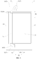
FIG. 1 is a structural schematic view of an electronic device according to one embodiment of the present disclosure. -
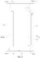
FIG. 2 is a structural schematic view of the electronic device according to another embodiment of the present disclosure. -
FIG. 3 is a structural schematic view of the electronic device according to another embodiment of the present disclosure. -
FIG. 4 is a structural schematic view of the electronic device according to another embodiment of the present disclosure. -
- Electronic device 100:
First side edge 11;Second side edge 12;Third side edge 13,Fourth side edge 14;Power interface 10; Firstsub power interface 101;Second power interface 102;Third power interface 103;Fourth power interface 104; -
Battery 2; -
Battery protection board 21;Cell 22; - Circuit board assembly 3:
-
First board 31;Second board 32; Firstflexible circuit board 33; Secondflexible circuit board 34;Transition board 30;Rigid circuit board 35; Thirdflexible circuit board 36. - The embodiments of the present disclosure will be described in detail below. Examples of the embodiments may be illustrated in the drawings. Same or similar reference numerals may be used to indicate same or similar elements or elements having same or similar functions. The embodiments described below with reference to the drawings are illustrative, and are not intended to be construed as limitations.
- The following disclosure provides many different embodiments or examples for implementing different structures of the present disclosure. In order to simplify the present disclosure, components and arrangements of specific examples are described below. Of course, these are merely examples, and are not intended to limit the present disclosure. In addition, reference numerals and/or reference letters are repeated in different examples of the present disclosure. The repetition is for the purpose of simplicity and clarity, and do not indicate the relationship between various embodiments and/or arrangements discussed herein. Moreover, examples of various specific processes and materials are provided in the present disclosure. However, those skilled in the art may recognize applications of other processes and/or usages of other materials. In the related art, during some electronic devices being charged, a current may arrive a second board first from a power interface, then be transported from the second board to a first board through a flexible circuit board, and further be transported from the first board to a battery through another flexible circuit board, and accordingly a charging path is relatively long. In response to the electronic devices are quickly charged in a current increasing manner, due to a current flowing path being relatively long and a current flow being relatively large, a current loss may be easy to be caused, such that a heat during the electronic devices being charged may be increased and a charging efficiency may be reduced. Furthermore, the electronic devices may be burnt, even safety accidents may be caused, such as the electronic devices on fire, the batteries explosions, and so on. Therefore, an
electronic device 100 is provided in the present disclosure and has a short charging path and low heat as charging, and high safety and so on. - An
electronic device 100 according to embodiments of the present disclosure will be described in the following, with reference to the accompanying drawings. - As shown in
FIG. 1 , theelectronic device 100 according to embodiments of the present disclosure may include ahousing 1, abattery 2 and acircuit board assembly 3. Apower interface 10 is defined on thehousing 1, thebattery 2 is arranged in thehousing 1 and includes abattery protection board 21 and acell 22. Thecircuit board 3 is arranged in thehousing 1, electrically connected to thepower interface 10. In this way, the battery may be get charged in response to thepower interface 10 being connected to a power outlet through a power cord and a power plug. - In
FIG. 1 , thecircuit board assembly 3 may include afirst board 31, asecond board 32, a firstflexible circuit board 33 and a secondflexible circuit board 34. Thefirst board 31 and thesecond board 32 are arranged at intervals along a first direction (direction F1 as shown inFIG. 1 ), and thebattery protection board 21 and thecell 22 are arranged in sequence along a second direction (direction F2 as shown inFIG. 1 ) substantially perpendicular to the first direction. The firstflexible circuit board 33 is connected to thebattery protection board 21 and thefirst board 31, and the secondflexible circuit board 34 is connected to thebattery protection board 21 and thesecond board 32. - That is, the
battery 2 is sandwiched between thefirst board 31 and thesecond board 32, and thebattery protection board 21 is located at a side of thecell 22, which is not the case that thebattery protection board 21 is located at a side of thebattery cell 22 close to thefirst board 31, or located at a side of thebattery cell 22 close to thesecond board 32. In this way, a length of the firstflexible circuit board 33 connecting thefirst board 31 and thebattery protection board 21 may be configured to be shorter, and a length of the secondflexible circuit board 33 connecting thesecond board 32 and thebattery protection board 21 may also be configured to be shorter. - In this way, through the
battery protection board 21 being located at the side of thecell 22, the firstflexible circuit board 33 being connected to thebattery protection board 21 and thefirst board 31, and the secondflexible circuit board 34 being connected to thebattery protection board 21 and thesecond board 32, a current transmission path between thebattery 2 and thefirst board 31 and a current transmission path between thebattery 2 and thesecond board 32 may be effectively reduced. In this way, whether thefirst board 31 and the firstflexible circuit board 33 are used to charge thebattery 2, or thesecond board 32 and the secondflexible circuit board 34 are used to charge thebattery 2, a charging path may be reduced. Heat generated as charging, charging efficiency and charging safety may be improved. In addition, in response to one of the firstflexible circuit board 33 and the secondflexible circuit board 34 is used to charge thebattery 2, the other one of the firstflexible circuit board 33 and the secondflexible circuit board 34 may be used to discharge thebattery 2, such that a power supply need may be satisfied and theelectronic device 100 may be ensured to be work normally. - For example, in embodiments shown in the
FIG. 1 andFIG. 2 , a length direction (the direction F1 as shown inFIG. 1 ) of thebattery protection board 21 is a direction from thefirst board 31 to thesecond board 32. That is, thefirst board 31 and thesecond board 32 are arranged at intervals along the length direction of thebattery protection board 21, thefirst board 31 is arranged at a side of thebattery 2, and thesecond board 32 is arranged at the other side of the battery. The firstflexible circuit board 33 is connected between thebattery protection board 21 and thefirst board 31, the secondflexible circuit board 34 is connected between thebattery protection board 21 and thesecond board 32. In this way, thefirst board 31 is arranged at one side of the length direction of thebattery protection board 21, and thesecond board 32 is arranged at the other side of the length direction of thebattery protection board 21, such that one end of the length direction of the battery protection board 21 (for example, a top end of thebattery protection board 21 shown in theFIG. 1 ) may be close to thefirst board 31, and the other end of the length direction of the battery protection board 21 (for example, a bottom end of thebattery protection board 21 shown in theFIG. 1 ) may be close to thesecond board 32. As a result, the current transmission path may be effectively reduced. - For example, in some specific embodiments of the present disclosure, the
power interface 10 is connected with thesecond board 32, in which case the secondflexible circuit board 34 may be used to the second board to charge thebattery 2, and the firstflexible circuit board 33 may be used to thebattery 2 to discharge the first board. Moreover, in the present embodiment, there are a plurality of ways for thesecond board 32 to obtain a discharge from thebattery 2, for example, thebattery 2 may discharge thesecond board 32 by the secondflexible circuit board 34 in response to thepower interface 10 being not connected to the power outlet. For another example, in response to thecircuit assembly 3 includes atransition board 30 connected to thefirst board 31 and thesecond board 32, thebattery 2 may also discharge thesecond board 32 by thetransition board 30, such that a discharge from the battery to thefirst board 31 may also be transited to thesecond board 32 through thetransition board 30. - Therefore, the
battery protection board 21 is arranged at a side of thebattery 2 such that thefirst board 31 may be arranged at one side of a length direction of thebattery protection board 21 and thesecond board 32 may be arranged at the other side of the length direction of thebattery protection board 21. In this way, two flexible circuit board may be extended out from thebattery protection board 21, that is, the firstflexible circuit board 33 used to connected to thefirst board 31 and the secondflexible circuit board 34 used to connected to thesecond board 32. Thus, in response to thesecond board 32 being connected to thepower interface 10, the secondflexible circuit board 34 may be used as a charging flexible circuit board to charge thebattery 2 through thesecond board 32 being connected to thepower interface 10, and the firstflexible circuit board 33 may be used as a discharging flexible circuit board to make thebattery 2 supply power to thefirst board 31. Similarly, in response to thefirst board 31 being connected to thepower interface 10, the firstflexible circuit board 33 may be used as a charging flexible circuit board to charge thebattery 2 through thefirst board 31 being connected to thepower interface 10, and the secondflexible circuit board 34 may be used as a discharging flexible circuit board to make thebattery 2 supply power to thesecond board 32. - A heating loss calculation formula during a charging process of the
battery 2 is P=I2R, wherein I is a charging current and R is a loop impedance, since the present disclosure can reduce a length of the flexible circuit board used to charge thebattery 2, a charging loop impedance R may be reduced, and a reduction amount of R is related to the length of thebattery 2, such that the heating loss may be reduced and the charging efficiency may be improved, which may be more significant in a case of high-current charging. - In short, the
electronic device 100 according to the embodiments of the present disclosure, since thefirst board 31 is arranged at one side of a length direction of thebattery protection board 21 and thesecond board 32 is arranged at the other side of the length direction of thebattery protection board 21, that is, thebattery 2 is arranged at a side portion between thefirst board 31 and thesecond board 32. Further, the firstflexible circuit board 33 and the secondflexible circuit board 34 are arranged, such that the charging path may be shortened to reduce the heating as charging, and the user experience may be improved. - It should be noted that a composition and function of "the
battery protection board 21" are well known to those skilled in the art. That is, for arechargeable battery 2, such as a lithium battery, an integrated circuit board acting as a protective role, etc., for example, for the rechargeable lithium battery, a reason why a protection is needed is determined by its own characteristics. A material of the lithium battery itself determines that it cannot be overcharged, over discharged, with an overcurrent, with a short circuit, and charged and discharged under an ultra-high temperature, thus the lithium battery always be with a protection board with a sampling resistor and a current fuse. Therefore, it will not be repeated here. - In addition, after a specific type of the
electronic device 100 is determined, a specific composition and function of the "thefirst board 31" and the "thesecond board 32" are also well known to those skilled in the art. For example, in a case that theelectronic device 100 is a smart phone, those skilled in the art can clearly understand what thefirst board 31" and "thesecond board 32" refer to. Of course, theelectronic device 100 according to the embodiments of the present disclosure is not limited to a smart phone, for example, may be a tablet computer, a vehicle-mounted computer, etc., and no limitation is made here. - It should be noted that the
cell 22 may be one or multiple, and thebattery protection board 21 is connected to tabs of each of thecells 22. In some embodiments of the present disclosure, thebattery 2 may have only onecell 22. In other embodiments of the present disclosure, thebattery 2 may also havemultiple cells 22, and themultiple cells 22 are connected in series and/or in shunts, that is, themultiple cells 22 may be connected in series, or themultiple cells 22 may be connected in shunts, or themultiple cells 22 may be connected first in series and then in shunts, or themultiple cells 22 may be connected first in shunts and then in series, etc. In this way, different practical requirements may be satisfied. - In some embodiments of the present disclosure, the
circuit board assembly 3 may include thetransition board 30 connected to the first board and the second board. In response to thebattery 2 discharging to thefirst board 31 through the firstflexible circuit board 33, thefirst board 31 may discharge to thesecond board 32 through thetransition board 30. In response to thebattery 2 discharging to thesecond board 32 through the secondflexible circuit board 34, thesecond board 32 may discharge to thefirst board 31 through thetransition board 30. In this way, the electronic device may be work normally. - In some specific embodiments of the present disclosure, as shown in
FIG. 1 , the transition board thetransition board 30 may include arigid circuit board 35 connected to the first board thefirst board 31 and the second board thesecond board 32, and therigid circuit board 35 is located on a side of the battery thebattery 2 away from the battery protection board thebattery protection board 21. For example, in the embodiment shown inFIG. 1 , in response to the battery protection board thebattery protection board 21 is located on a right side of thebattery 2, therigid circuit board 35 is located on a left side of thebattery 2, such that a space may be more fully utilized and an assembly may be facilitated. - In some specific embodiments of the present disclosure, in
FIG. 2 , thetransition board 30 may include a thirdflexible circuit board 36 connected to thefirst board 31 and thesecond board 32, and the thirdflexible circuit board 36 is arranged on a thickness side of thebattery 2. In this way, there may be more accommodating space for thebattery 2 to be reserved such that a capacity of thebattery 2 may be larger to satisfy a longer standby time. - In some embodiments, as shown in
FIG. 1 , thebattery protection board 21 is arranged at the side portion between thefirst board 31 and thesecond board 32. A meaning of "the side portion between thefirst board 31 and thesecond board 32" will be explained in the following, that is, the length direction of thebattery protection board 21 is defined to be the first direction F1, the first direction F1 is substantially perpendicular to the second direction F2. Two ends of thefirst board 31 in the second direction F2 are a first end and second end, and two ends of thesecond board 32 in the second direction F2 are a third end and a fourth end. The first end is opposite to the second end in the first direction F1, and the third end is opposite to the fourth end in the first direction F1. Thebattery protection board 21 is arranged between the first end and the third end, or between the second and the fourth end. That is, thebattery protection board 21 is arranged close to a side edge between thefirst board 31 and thesecond board 32, such that an accommodating space for thecell 22 may be increased and the capacity and endurance of thebattery 2 may be improved. - As shown in
FIG. 1 , the firstflexible circuit board 33 is connected to a side portion of thefirst board 31 close to thebattery protection board 21, and the secondflexible circuit board 34 is connected to a side portion of thesecond board 32 close to thebattery protection board 21. In this way, the length of the firstflexible circuit board 33 may be further shortened, and the length of the secondflexible circuit board 34 may be further shortened. As a result, the charging path may be shortened to reduce the heating as charging, and the user experience may be improved. For example, in the embodiments shown inFIG. 1 , in response to thebattery protection board 21 being arranged at a right side portion between thefirst board 31 and thesecond board 32, the firstflexible circuit board 33 is connected to a right end of thefirst board 31, and the secondflexible circuit board 34 is connected to a right end of thesecond board 32. - As shown in
FIG. 1 , the firstflexible circuit board 33 is connected to one end of the length direction of thebattery protection board 21, and the secondflexible circuit board 34 is connected to the other end of the length direction of thebattery protection board 21. In this way, the length of the firstflexible circuit board 33 may be further shortened, and the length of the secondflexible circuit board 34 may be further shortened. As a result, the charging path may be shortened to reduce the heating as charging, and the user experience may be improved. For example, in the specific embodiment shown inFIG. 1 , the length direction of thebattery protection board 21 is an up-down direction. The firstflexible circuit board 33 may be connected to a top end of thebattery protection board 21, and the secondflexible circuit board 34 may be connected to a bottom end of thebattery protection board 21. Of course, the present disclosure is not limited to thereto, the firstflexible circuit board 33 and the secondflexible circuit board 34 may also be connected to other parts of thebattery protection board 21 to better satisfy different actual requirements. - In some embodiments, as shown in
FIG. 1 , the length direction of the battery protection board 21 (for example, the F1 direction shown inFIG. 1 ) may be a length direction of theelectronic device 100. Therefore, for most electronic devices, there is no need to greatly improve structure types of thefirst board 31 and thesecond board 32, and there is also no need to greatly improve an overall layout of the electronic devices. In this way, it may be more convenient for a mass production and a production cost may be reduced. - In some embodiments, as shown in
FIG. 1 , thehousing 1 may include afirst side edge 11, asecond side edge 12 opposite to and substantially parallel to thefirst side edge 11, athird side edge 13, and afourth side edge 14 opposite to and substantially parallel to thethird side edge 13. Thefirst side edge 11 is arranged at one side of a length direction of thethird side edge 13 and thefourth side edge 14, and thesecond side edge 12 is arranged at the other side portion of thethird side edge 13 and thefourth side edge 14. Thefirst board 31 is arranged at a side portion of thesecond board 32 close to thefirst side edge 11, thesecond board 32 is arranged at a side portion of the first board 31close to thesecond side edge 12, and thebattery protection board 21 is substantially parallel to thethird side edge 13 and thefourth side edge 14. In this way, a structure of thehousing 1 may be simple, so as to facilitate producing and processing, and facilitate an assembly of thefirst board 31, thesecond board 32 and thebattery 2. - It should be noted that a number and a specific arrangement location of the
power interface 10 are not limited. The specific locations of thepower interface 10 in some embodiments of the present disclosure will be described in the following, but the present disclosure is not limited to the following embodiments. - For example, in the embodiments shown in
FIG. 1 , thepower interface 10 may include a firstsub power interface 101 arranged on thefirst side edge 11, and the firstsub power interface 101 is electrically connected to thefirst board 31 to charge thebattery 2 through the firstflexible circuit board 33. That is, in response to the firstsub power interface 101 being connected to the power outlet, thefirst board 31 may charge thebattery 2 through the firstflexible circuit board 33, and thebattery 2 may discharge to thesecond board 32 through the secondflexible circuit board 34. In this way, since a distance between thefirst side edge 11 and thefirst board 31 is relatively short, a distance between the firstsub power interface 101 and thefirst board 31 may be shortened, and the charging path may be further shortened, so as to reduce the heating as charging and improve the user experience. - For example, in the embodiments shown in
FIG. 1 , thepower interface 10 may include a secondsub power interface 102 arranged on thesecond side edge 12, and the secondsub power interface 102 is electrically connected to thesecond board 32 to charge thebattery 2 through the secondflexible circuit board 34. That is, in response to the secondsub power interface 102 being connected to the power outlet, thesecond board 32 may charge thebattery 2 through the secondflexible circuit board 34, and thebattery 2 may discharge to thefirst board 31 through the firstflexible circuit board 33. In this way, since a distance between thesecond side edge 12 and thesecond board 32 is relatively short, a distance between the secondsub power interface 102 and thesecond board 32 may be shortened, and the charging path may be further shortened, so as to reduce the heating as charging and improve the user experience. - For example, in the embodiments shown in
FIG. 1 , thepower interface 10 may include a thirdsub power interface 103 arranged on thethird side edge 13, the thirdsub power interface 103 is located in an orthographic projection (for example, A region shown inFIG. 1 ) of thefirst board 31 on thethird side edge 13, and electrically connected to thefirst board 31 to charge thebattery 2 through the firstflexible circuit board 33. That is, in response to the thirdsub power interface 103 being connected to the power outlet, thefirst board 31 may charge thebattery 2 through the firstflexible circuit board 33, and thebattery 2 may discharge to thesecond board 32 through the secondflexible circuit board 34. In this way, since a distance between the thirdsub power interface 103 and thefirst board 31 is relatively short, the charging path may be further shortened to reduce the heating as charging and improve the user experience. In addition, in the present embodiment, in response to a distance L1 between thebattery protection board 21 and thethird side edge 13 being less than a distance L2 between thebattery protection board 21 and thefourth side edge 14, a distance between the firstflexible circuit board 33 and the thirdsub power interface 103 may be further shortened, such that a power transferring length from the thirdsub power interface 103 to the firstflexible circuit board 33 may be shortened. In this way, the charging path may be further shortened, so as to reduce the heating as charging and improve the user experience. - For example, in the embodiments shown in
FIG. 1 , thepower interface 10 may include a fourthsub power interface 104 arranged on thethird side edge 13, the fourthsub power interface 104 is located in an orthographic projection of thesecond board 32 on thefourth side edge 14, and electrically connected to thesecond board 32 to charge thebattery 2 through the secondflexible circuit board 34. That is, in response to the fourthsub power interface 104 being connected to the power outlet, thesecond board 32 may charge thebattery 2 through the secondflexible circuit board 34, and thebattery 2 may discharge to thefirst board 31 through the firstflexible circuit board 33. In this way, since a distance between the fourthsub power interface 104 and thesecond board 32 is relatively short, the charging path may be further shortened, so as to reduce the heating as charging and improve the user experience. In addition, in the present embodiment, in response to the distance L1 between thebattery protection board 21 and thethird side edge 13 being less than the distance L2 between thebattery protection board 21 and thefourth side edge 14, a distance between the secondflexible circuit board 34 and the fourthsub power interface 104 may be further shortened, such that a power transferring length from the fourthsub power interface 104 to the secondflexible circuit board 34 may be shortened. In this way, the charging path may be further shortened, so as to reduce the heating as charging and improve the user experience. - In a specific embodiment of the present disclosure, the
battery 2 is configured to be a structure where thebattery protection board 21 is arranged on a side, the firstflexible circuit board 33 extends out from one end of thebattery protection board 21 and connected to thefirst board 31, and the secondflexible circuit board 34 extends out from the other end of thebattery protection board 21 and connected to thefirst board 31. Thepower interface 10 is arranged at a position close to thesecond board 32. Thesecondary board 32 charges thebattery 2 through the secondflexible circuit board 34, and thebattery 2 discharges to thefirst board 31 through the firstflexible circuit board 33, so as to shorten the charging path and improve a charging effect. In addition, in the embodiments of the present disclosure, thepower interface 10 may be arranged at a bottom, a side, or even a top of theelectronic device 100, such that the charging path may be shortened, the heating as charging may be reduced, and the user experience may be improved. Moreover, in the embodiments of the present disclosure, thefirst board 31 and thesecond board 32 may be arranged to be a separate form by the thirdflexible circuit board 36, or may be arranged to be an integral form by therigid circuit board 35, which is not limited. - In a specific embodiment of the present disclosure, in
FIGS. 1 and2 , theelectronic device 100 includes: ahousing 1 including afirst side edge 11, asecond side edge 12 opposite to and substantially parallel to thefirst side edge 11, and having apower interface 10, athird side edge 13 substantially perpendicular to thefirst side edge 11, and afourth side edge 14 opposite to and substantially parallel to thethird side edge 13; abattery 2 arranged in thehousing 1 and including acell 22, and abattery protection board 21 arranged at a side of thecell 22 close to thethird side edge 13 or thesecond side edge 12; and acircuit board assembly 3 arranged in thehousing 1, electrically connected to thepower interface 10 and including afirst board 31 arranged at a side of thebattery 2 close to thefirst side edge 11, asecond board 32 arranged at a side of thebattery 2 close to thesecond side edge 12, a firstflexible circuit board 33 connected thebattery protection board 21 and thefirst board 31, and a secondflexible circuit board 34 connected thebattery protection board 21 and thesecond board 32. In the present embodiment, thebattery protection board 21 is arranged on a side portion of theelectronic device 100, such that theelectronic device 100 may have a simple structure and the charging path may be short. - Of course, the present disclosure is not limited to thereto. In other embodiments of the present disclosure, the
battery protection board 21 may also be arranged in other positions of theelectronic device 100. For example, in the embodiment shown inFIG. 3 , thebattery protection board 21 may be arranged between therigid circuit board 35 and thecell 22. For a further example, in the embodiment shown inFIG. 4 , thebattery protection board 21 may be arranged between the twocells 22, located in a center position of theelectronic device 100, etc., which will not be repeated herein. - In addition, other configurations and operations of the
electronic device 100 according to the embodiments of the present disclosure are known to those of ordinary skill in the art after the type of theelectronic device 100 is determined, which will not be described in detail here. - In the description of the present specification, the description with reference to the terms "one embodiment", "some embodiments", "illustrative embodiment", "example", "specific example", or "some examples", and the like, means that a specific feature, structure, material, or characteristic described in connection with the embodiment or example is included in at least one embodiment or example of the present disclosure. Thus, the illustrative descriptions of the terms throughout this specification are not necessarily referring to the same embodiment or example of the present disclosure. Furthermore, the specific features, structures, materials, or characteristics may be combined in any suitable manner in one or more embodiments or examples. In addition, various embodiments or examples described in the specification and features of various embodiments or examples, may be incorporated and combined by those skilled in the art in case of an absence of confliction.
- Although the embodiments of the present disclosure have been shown and described, those of ordinary skill in the art can understand that various changes, modifications, substitutions and variations can be made to the embodiments without departing from the principle and purpose of the present disclosure. The scope of the present disclosure is defined by the claims and the equivalents of the claims.
Claims (16)
- An electronic device, comprising:a housing, defined with a power interface on the housing;a battery, arranged in the housing, and comprising:a battery protection board; anda cell;a circuit board assembly, arranged in the housing, electrically connected to the power interface, and comprising:a first board, located at one side of the battery;a second board, located at the other side of the battery;a first flexible circuit board, connected to the battery protection board and the first board; anda second flexible circuit board, connected to the battery protection board and the second board;wherein the first board and the second board are arranged at intervals along a first direction, and the battery protection board and the cell are arranged in sequence along a second direction substantially perpendicular to the first direction.
- The electronic device according to claim 1, wherein a length direction of the battery protection board is a direction from the first board to the second board, and the battery protection board is arranged at a side portion between the first board and the second board.
- The electronic device according to claim 2, wherein the first flexible circuit board is connected to a side portion of the first board close to the battery protection board, and the second flexible circuit board is connected to a side portion of the second board close to the battery protection board.
- The electronic device according to any one of claims 1-3, wherein the first flexible circuit board is connected to one end of a length direction of the battery protection board, and the second flexible circuit board is connected to the other end of the length direction of the battery protection board.
- The electronic device according to any one of claims 1-4, wherein the length direction of the battery protection board is a length direction of the electronic device.
- The electronic device according to claim 5, wherein the housing comprises:a first side edge;a second side edge, opposite to and substantially parallel to the first side edge;a third side edge; anda fourth side edge, opposite to and substantially parallel to the third side edge;wherein the first side edge is arranged at one side of a length direction of the third side edge and the fourth side edge, the second side edge is arranged at the other side of the length direction of the third side edge and the fourth side edge, the first board is arranged at a side of the second board close to the first side edge, the second board is arranged at a side of the first board close to the second side edge, and the battery protection board is substantially parallel to the third side edge and the fourth side edge.
- The electronic device according to claim 6, wherein the power interface comprises a first sub power interface arranged on the first side edge, and the first sub power interface is electrically connected to the first board to charge the battery through the first flexible circuit board.
- The electronic device according to claim 6 or 7, wherein the power interface comprises a second sub power interface arranged on the second side edge, and the second sub power interface is electrically connected to the second board to charge the battery through the second flexible circuit board.
- The electronic device according to any one of claims 6-8, wherein the power interface comprises a third sub power interface arranged on the third side edge, the third sub power interface is located in an orthographic projection of the first board on the third side edge, and electrically connected to the first board to charge the battery through the first flexible circuit board.
- The electronic device according to any one of claims 6-9, wherein the power interface comprises a fourth sub power interface arranged on the third side edge, the fourth sub power interface is located in an orthographic projection of the second board on the fourth third side edge, and electrically connected to the second board to charge the battery through the second flexible circuit board.
- The electronic device according to claim 9 or 10, wherein a distance L1 between the battery protection board fourth side edge and the third side edge is less than that L2 between the battery protection board and the fourth side edge.
- The electronic device according to any one of claims 1-11, wherein the circuit board assembly further comprises a transition board connected to the first board and the second board.
- The electronic device according to claim 12, wherein the transition board comprises a rigid circuit board connected to the first board and the second board, and the rigid circuit board is located on a side of the battery away from the battery protection board.
- The electronic device according to claim 12, wherein the transition board comprises a third flexible circuit board connected to the first board and the second board, and the third flexible circuit is arranged on a thickness side of the battery.
- The electronic device according to any one of claims 1-14, wherein the cells are multiple, the multiple cells are connected in series and/or in shunts, and the battery protection board is connected to tabs of each of the cells.
- An electronic device, comprising:a housing, comprising:a first side edge;a second side edge, opposite to and substantially parallel to the first side edge, and having a power interface;a third side edge, substantially perpendicular to the first side edge; anda fourth side edge, opposite to and substantially parallel to the third side edge;a battery, arranged in the housing, comprising:a cell; anda battery protection board, arranged at a side of the cell close to the third side edge or the second side edge; anda circuit board assembly, arranged in the housing, electrically connected to the power interface, and comprising:a first board, arranged at a side of the battery close to the first side edge;a second board, arranged at a side of the battery close to the second side edge;a first flexible circuit board, connected the battery protection board and the first board; anda second flexible circuit board, connected the battery protection board and the second board.
Applications Claiming Priority (3)
| Application Number | Priority Date | Filing Date | Title |
|---|---|---|---|
| CN201921695254.4U CN210984782U (en) | 2019-10-09 | 2019-10-09 | Electronic device |
| CN201910955492.2A CN112652856B (en) | 2019-10-09 | 2019-10-09 | Electronic equipment |
| PCT/CN2020/113172 WO2021068690A1 (en) | 2019-10-09 | 2020-09-03 | Electronic device |
Publications (3)
| Publication Number | Publication Date |
|---|---|
| EP4037086A1 true EP4037086A1 (en) | 2022-08-03 |
| EP4037086A4 EP4037086A4 (en) | 2022-12-14 |
| EP4037086B1 EP4037086B1 (en) | 2024-02-07 |
Family
ID=75437688
Family Applications (1)
| Application Number | Title | Priority Date | Filing Date |
|---|---|---|---|
| EP20875177.6A Active EP4037086B1 (en) | 2019-10-09 | 2020-09-03 | Electronic device |
Country Status (3)
| Country | Link |
|---|---|
| US (1) | US12328021B2 (en) |
| EP (1) | EP4037086B1 (en) |
| WO (1) | WO2021068690A1 (en) |
Family Cites Families (15)
| Publication number | Priority date | Publication date | Assignee | Title |
|---|---|---|---|---|
| JP2003272584A (en) * | 2002-03-13 | 2003-09-26 | Tocad Energy Co Ltd | Internal structure of battery pack |
| US8395256B2 (en) * | 2007-02-02 | 2013-03-12 | Harris Stratex Networks Operating Corporation | Packaging for low-cost, high-performance microwave and millimeter wave modules |
| KR100954589B1 (en) * | 2007-02-07 | 2010-04-26 | 삼성에스디아이 주식회사 | Protective circuit assembly and battery pack having same |
| US9553342B2 (en) * | 2013-05-16 | 2017-01-24 | Samsung Sdi Co., Ltd. | Battery pack |
| US20150255776A1 (en) * | 2014-03-06 | 2015-09-10 | Apple Inc. | Battery Pack System |
| CN204291066U (en) | 2014-11-14 | 2015-04-22 | 上海闻泰电子科技有限公司 | There is the mobile phone of drawing and pulling type battery |
| CN205071069U (en) | 2015-10-19 | 2016-03-02 | 上海与德通讯技术有限公司 | Mobile terminal with front camera and large LCD |
| KR102651576B1 (en) * | 2016-10-18 | 2024-03-27 | 삼성전자주식회사 | electronic device including battery module and manufacturing method thereof |
| CN106790785A (en) * | 2016-11-29 | 2017-05-31 | 努比亚技术有限公司 | A kind of mobile terminal charging structure and mobile terminal |
| US20180288889A1 (en) * | 2017-03-30 | 2018-10-04 | Google Inc. | Circuit board and battery architecture of an electronic device |
| WO2019018990A1 (en) * | 2017-07-24 | 2019-01-31 | 华为技术有限公司 | Battery pack and electronic equipment |
| CN207410590U (en) * | 2017-09-11 | 2018-05-25 | 广东欧珀移动通信有限公司 | Circuit connection structure and terminal |
| CN207320267U (en) | 2017-09-19 | 2018-05-04 | 奇酷互联网络科技(深圳)有限公司 | A kind of battery connecting construction and electronic equipment |
| CN210984782U (en) * | 2019-10-09 | 2020-07-10 | Oppo广东移动通信有限公司 | Electronic device |
| CN210866339U (en) * | 2019-12-17 | 2020-06-26 | 维沃移动通信有限公司 | Electronic equipment |
-
2020
- 2020-09-03 EP EP20875177.6A patent/EP4037086B1/en active Active
- 2020-09-03 WO PCT/CN2020/113172 patent/WO2021068690A1/en not_active Ceased
-
2022
- 2022-04-07 US US17/715,714 patent/US12328021B2/en active Active
Also Published As
| Publication number | Publication date |
|---|---|
| WO2021068690A1 (en) | 2021-04-15 |
| EP4037086A4 (en) | 2022-12-14 |
| US12328021B2 (en) | 2025-06-10 |
| US20220231528A1 (en) | 2022-07-21 |
| EP4037086B1 (en) | 2024-02-07 |
Similar Documents
| Publication | Publication Date | Title |
|---|---|---|
| CN210984782U (en) | Electronic device | |
| CN105264689B (en) | Circuit board for secondary cell and the battery pack including the circuit board | |
| CN111082493B (en) | Terminal Equipment | |
| KR102720302B1 (en) | Busbars, batteries and electrical devices | |
| KR102711055B1 (en) | Battery module and battery pack including the same | |
| KR100571231B1 (en) | Fuse device of lithium ion battery | |
| JP6639788B2 (en) | Protection device for secondary battery | |
| KR102505612B1 (en) | Battery pack | |
| EP3073548B1 (en) | Battery pack | |
| EP4075579A1 (en) | Battery assembly for use in terminal device, and terminal device having same | |
| KR20200020565A (en) | Battery module including battery management system with improved assembly structure | |
| WO2017219359A1 (en) | Multi-lug battery | |
| CN104577995A (en) | Lithium battery protection circuit device with fly-wheel circuit | |
| US12328021B2 (en) | Electronic device | |
| CN206893745U (en) | Battery module with power balance structure | |
| CN112652856B (en) | Electronic equipment | |
| EP3255702B1 (en) | Battery pack | |
| KR102284774B1 (en) | Battery pack for preventing short circuit | |
| KR102124626B1 (en) | Secondary battery | |
| CN106786914A (en) | A kind of charging module and electronic equipment | |
| CN218513642U (en) | Protection plate and battery | |
| CN210469888U (en) | MOS pipe parallel structure, lithium battery charging protection board and vehicle | |
| US9142826B1 (en) | Battery pack | |
| KR102375844B1 (en) | Low-resistance Battery Protection Circuit For Protecting Electrostatic Discharge | |
| CN107134558A (en) | Battery Modules and Notebooks |
Legal Events
| Date | Code | Title | Description |
|---|---|---|---|
| STAA | Information on the status of an ep patent application or granted ep patent |
Free format text: STATUS: THE INTERNATIONAL PUBLICATION HAS BEEN MADE |
|
| PUAI | Public reference made under article 153(3) epc to a published international application that has entered the european phase |
Free format text: ORIGINAL CODE: 0009012 |
|
| STAA | Information on the status of an ep patent application or granted ep patent |
Free format text: STATUS: REQUEST FOR EXAMINATION WAS MADE |
|
| 17P | Request for examination filed |
Effective date: 20220428 |
|
| AK | Designated contracting states |
Kind code of ref document: A1 Designated state(s): AL AT BE BG CH CY CZ DE DK EE ES FI FR GB GR HR HU IE IS IT LI LT LU LV MC MK MT NL NO PL PT RO RS SE SI SK SM TR |
|
| A4 | Supplementary search report drawn up and despatched |
Effective date: 20221111 |
|
| RIC1 | Information provided on ipc code assigned before grant |
Ipc: G06F 1/26 20060101ALI20221107BHEP Ipc: G06F 1/16 20060101ALI20221107BHEP Ipc: H04M 1/02 20060101ALI20221107BHEP Ipc: H01M 10/42 20060101ALI20221107BHEP Ipc: H01M 50/50 20210101AFI20221107BHEP |
|
| DAV | Request for validation of the european patent (deleted) | ||
| DAX | Request for extension of the european patent (deleted) | ||
| REG | Reference to a national code |
Ref country code: DE Ref legal event code: R079 Free format text: PREVIOUS MAIN CLASS: H01M0050500000 Ipc: H02J0007000000 Ref country code: DE Ref legal event code: R079 Ref document number: 602020025464 Country of ref document: DE Free format text: PREVIOUS MAIN CLASS: H01M0050500000 Ipc: H02J0007000000 |
|
| GRAP | Despatch of communication of intention to grant a patent |
Free format text: ORIGINAL CODE: EPIDOSNIGR1 |
|
| STAA | Information on the status of an ep patent application or granted ep patent |
Free format text: STATUS: GRANT OF PATENT IS INTENDED |
|
| RIC1 | Information provided on ipc code assigned before grant |
Ipc: H01M 10/42 20060101ALI20230620BHEP Ipc: H04M 1/02 20060101ALI20230620BHEP Ipc: G06F 1/16 20060101ALI20230620BHEP Ipc: G06F 1/26 20060101ALI20230620BHEP Ipc: H01M 50/50 20210101ALI20230620BHEP Ipc: H05K 1/14 20060101ALI20230620BHEP Ipc: H02J 7/00 20060101AFI20230620BHEP |
|
| INTG | Intention to grant announced |
Effective date: 20230704 |
|
| GRAJ | Information related to disapproval of communication of intention to grant by the applicant or resumption of examination proceedings by the epo deleted |
Free format text: ORIGINAL CODE: EPIDOSDIGR1 |
|
| STAA | Information on the status of an ep patent application or granted ep patent |
Free format text: STATUS: REQUEST FOR EXAMINATION WAS MADE |
|
| GRAP | Despatch of communication of intention to grant a patent |
Free format text: ORIGINAL CODE: EPIDOSNIGR1 |
|
| STAA | Information on the status of an ep patent application or granted ep patent |
Free format text: STATUS: GRANT OF PATENT IS INTENDED |
|
| INTC | Intention to grant announced (deleted) | ||
| RIC1 | Information provided on ipc code assigned before grant |
Ipc: H01M 50/519 20210101ALI20231016BHEP Ipc: H01M 50/284 20210101ALI20231016BHEP Ipc: H05K 1/14 20060101ALI20231016BHEP Ipc: H01M 50/50 20210101ALI20231016BHEP Ipc: G06F 1/26 20060101ALI20231016BHEP Ipc: G06F 1/16 20060101ALI20231016BHEP Ipc: H04M 1/02 20060101ALI20231016BHEP Ipc: H01M 10/42 20060101ALI20231016BHEP Ipc: H02J 7/00 20060101AFI20231016BHEP |
|
| INTG | Intention to grant announced |
Effective date: 20231031 |
|
| GRAS | Grant fee paid |
Free format text: ORIGINAL CODE: EPIDOSNIGR3 |
|
| GRAA | (expected) grant |
Free format text: ORIGINAL CODE: 0009210 |
|
| STAA | Information on the status of an ep patent application or granted ep patent |
Free format text: STATUS: THE PATENT HAS BEEN GRANTED |
|
| AK | Designated contracting states |
Kind code of ref document: B1 Designated state(s): AL AT BE BG CH CY CZ DE DK EE ES FI FR GB GR HR HU IE IS IT LI LT LU LV MC MK MT NL NO PL PT RO RS SE SI SK SM TR |
|
| REG | Reference to a national code |
Ref country code: GB Ref legal event code: FG4D |
|
| REG | Reference to a national code |
Ref country code: CH Ref legal event code: EP |
|
| REG | Reference to a national code |
Ref country code: IE Ref legal event code: FG4D |
|
| REG | Reference to a national code |
Ref country code: DE Ref legal event code: R096 Ref document number: 602020025464 Country of ref document: DE |
|
| REG | Reference to a national code |
Ref country code: LT Ref legal event code: MG9D |
|
| REG | Reference to a national code |
Ref country code: NL Ref legal event code: MP Effective date: 20240207 |
|
| P01 | Opt-out of the competence of the unified patent court (upc) registered |
Effective date: 20240521 |
|
| PG25 | Lapsed in a contracting state [announced via postgrant information from national office to epo] |
Ref country code: IS Free format text: LAPSE BECAUSE OF FAILURE TO SUBMIT A TRANSLATION OF THE DESCRIPTION OR TO PAY THE FEE WITHIN THE PRESCRIBED TIME-LIMIT Effective date: 20240607 |
|
| PG25 | Lapsed in a contracting state [announced via postgrant information from national office to epo] |
Ref country code: LT Free format text: LAPSE BECAUSE OF FAILURE TO SUBMIT A TRANSLATION OF THE DESCRIPTION OR TO PAY THE FEE WITHIN THE PRESCRIBED TIME-LIMIT Effective date: 20240207 |
|
| PG25 | Lapsed in a contracting state [announced via postgrant information from national office to epo] |
Ref country code: GR Free format text: LAPSE BECAUSE OF FAILURE TO SUBMIT A TRANSLATION OF THE DESCRIPTION OR TO PAY THE FEE WITHIN THE PRESCRIBED TIME-LIMIT Effective date: 20240508 |
|
| REG | Reference to a national code |
Ref country code: AT Ref legal event code: MK05 Ref document number: 1655996 Country of ref document: AT Kind code of ref document: T Effective date: 20240207 |
|
| PG25 | Lapsed in a contracting state [announced via postgrant information from national office to epo] |
Ref country code: HR Free format text: LAPSE BECAUSE OF FAILURE TO SUBMIT A TRANSLATION OF THE DESCRIPTION OR TO PAY THE FEE WITHIN THE PRESCRIBED TIME-LIMIT Effective date: 20240207 Ref country code: NL Free format text: LAPSE BECAUSE OF FAILURE TO SUBMIT A TRANSLATION OF THE DESCRIPTION OR TO PAY THE FEE WITHIN THE PRESCRIBED TIME-LIMIT Effective date: 20240207 Ref country code: RS Free format text: LAPSE BECAUSE OF FAILURE TO SUBMIT A TRANSLATION OF THE DESCRIPTION OR TO PAY THE FEE WITHIN THE PRESCRIBED TIME-LIMIT Effective date: 20240507 |
|
| PG25 | Lapsed in a contracting state [announced via postgrant information from national office to epo] |
Ref country code: ES Free format text: LAPSE BECAUSE OF FAILURE TO SUBMIT A TRANSLATION OF THE DESCRIPTION OR TO PAY THE FEE WITHIN THE PRESCRIBED TIME-LIMIT Effective date: 20240207 |
|
| PG25 | Lapsed in a contracting state [announced via postgrant information from national office to epo] |
Ref country code: AT Free format text: LAPSE BECAUSE OF FAILURE TO SUBMIT A TRANSLATION OF THE DESCRIPTION OR TO PAY THE FEE WITHIN THE PRESCRIBED TIME-LIMIT Effective date: 20240207 |
|
| PG25 | Lapsed in a contracting state [announced via postgrant information from national office to epo] |
Ref country code: RS Free format text: LAPSE BECAUSE OF FAILURE TO SUBMIT A TRANSLATION OF THE DESCRIPTION OR TO PAY THE FEE WITHIN THE PRESCRIBED TIME-LIMIT Effective date: 20240507 Ref country code: NO Free format text: LAPSE BECAUSE OF FAILURE TO SUBMIT A TRANSLATION OF THE DESCRIPTION OR TO PAY THE FEE WITHIN THE PRESCRIBED TIME-LIMIT Effective date: 20240507 Ref country code: NL Free format text: LAPSE BECAUSE OF FAILURE TO SUBMIT A TRANSLATION OF THE DESCRIPTION OR TO PAY THE FEE WITHIN THE PRESCRIBED TIME-LIMIT Effective date: 20240207 Ref country code: LT Free format text: LAPSE BECAUSE OF FAILURE TO SUBMIT A TRANSLATION OF THE DESCRIPTION OR TO PAY THE FEE WITHIN THE PRESCRIBED TIME-LIMIT Effective date: 20240207 Ref country code: IS Free format text: LAPSE BECAUSE OF FAILURE TO SUBMIT A TRANSLATION OF THE DESCRIPTION OR TO PAY THE FEE WITHIN THE PRESCRIBED TIME-LIMIT Effective date: 20240607 Ref country code: HR Free format text: LAPSE BECAUSE OF FAILURE TO SUBMIT A TRANSLATION OF THE DESCRIPTION OR TO PAY THE FEE WITHIN THE PRESCRIBED TIME-LIMIT Effective date: 20240207 Ref country code: GR Free format text: LAPSE BECAUSE OF FAILURE TO SUBMIT A TRANSLATION OF THE DESCRIPTION OR TO PAY THE FEE WITHIN THE PRESCRIBED TIME-LIMIT Effective date: 20240508 Ref country code: FI Free format text: LAPSE BECAUSE OF FAILURE TO SUBMIT A TRANSLATION OF THE DESCRIPTION OR TO PAY THE FEE WITHIN THE PRESCRIBED TIME-LIMIT Effective date: 20240207 Ref country code: ES Free format text: LAPSE BECAUSE OF FAILURE TO SUBMIT A TRANSLATION OF THE DESCRIPTION OR TO PAY THE FEE WITHIN THE PRESCRIBED TIME-LIMIT Effective date: 20240207 Ref country code: BG Free format text: LAPSE BECAUSE OF FAILURE TO SUBMIT A TRANSLATION OF THE DESCRIPTION OR TO PAY THE FEE WITHIN THE PRESCRIBED TIME-LIMIT Effective date: 20240207 Ref country code: AT Free format text: LAPSE BECAUSE OF FAILURE TO SUBMIT A TRANSLATION OF THE DESCRIPTION OR TO PAY THE FEE WITHIN THE PRESCRIBED TIME-LIMIT Effective date: 20240207 |
|
| PG25 | Lapsed in a contracting state [announced via postgrant information from national office to epo] |
Ref country code: PL Free format text: LAPSE BECAUSE OF FAILURE TO SUBMIT A TRANSLATION OF THE DESCRIPTION OR TO PAY THE FEE WITHIN THE PRESCRIBED TIME-LIMIT Effective date: 20240207 Ref country code: PT Free format text: LAPSE BECAUSE OF FAILURE TO SUBMIT A TRANSLATION OF THE DESCRIPTION OR TO PAY THE FEE WITHIN THE PRESCRIBED TIME-LIMIT Effective date: 20240607 |
|
| PG25 | Lapsed in a contracting state [announced via postgrant information from national office to epo] |
Ref country code: SE Free format text: LAPSE BECAUSE OF FAILURE TO SUBMIT A TRANSLATION OF THE DESCRIPTION OR TO PAY THE FEE WITHIN THE PRESCRIBED TIME-LIMIT Effective date: 20240207 Ref country code: PT Free format text: LAPSE BECAUSE OF FAILURE TO SUBMIT A TRANSLATION OF THE DESCRIPTION OR TO PAY THE FEE WITHIN THE PRESCRIBED TIME-LIMIT Effective date: 20240607 Ref country code: PL Free format text: LAPSE BECAUSE OF FAILURE TO SUBMIT A TRANSLATION OF THE DESCRIPTION OR TO PAY THE FEE WITHIN THE PRESCRIBED TIME-LIMIT Effective date: 20240207 Ref country code: LV Free format text: LAPSE BECAUSE OF FAILURE TO SUBMIT A TRANSLATION OF THE DESCRIPTION OR TO PAY THE FEE WITHIN THE PRESCRIBED TIME-LIMIT Effective date: 20240207 |
|
| PG25 | Lapsed in a contracting state [announced via postgrant information from national office to epo] |
Ref country code: DK Free format text: LAPSE BECAUSE OF FAILURE TO SUBMIT A TRANSLATION OF THE DESCRIPTION OR TO PAY THE FEE WITHIN THE PRESCRIBED TIME-LIMIT Effective date: 20240207 |
|
| PG25 | Lapsed in a contracting state [announced via postgrant information from national office to epo] |
Ref country code: SM Free format text: LAPSE BECAUSE OF FAILURE TO SUBMIT A TRANSLATION OF THE DESCRIPTION OR TO PAY THE FEE WITHIN THE PRESCRIBED TIME-LIMIT Effective date: 20240207 |
|
| PG25 | Lapsed in a contracting state [announced via postgrant information from national office to epo] |
Ref country code: CZ Free format text: LAPSE BECAUSE OF FAILURE TO SUBMIT A TRANSLATION OF THE DESCRIPTION OR TO PAY THE FEE WITHIN THE PRESCRIBED TIME-LIMIT Effective date: 20240207 Ref country code: EE Free format text: LAPSE BECAUSE OF FAILURE TO SUBMIT A TRANSLATION OF THE DESCRIPTION OR TO PAY THE FEE WITHIN THE PRESCRIBED TIME-LIMIT Effective date: 20240207 |
|
| PG25 | Lapsed in a contracting state [announced via postgrant information from national office to epo] |
Ref country code: SK Free format text: LAPSE BECAUSE OF FAILURE TO SUBMIT A TRANSLATION OF THE DESCRIPTION OR TO PAY THE FEE WITHIN THE PRESCRIBED TIME-LIMIT Effective date: 20240207 |
|
| PG25 | Lapsed in a contracting state [announced via postgrant information from national office to epo] |
Ref country code: SM Free format text: LAPSE BECAUSE OF FAILURE TO SUBMIT A TRANSLATION OF THE DESCRIPTION OR TO PAY THE FEE WITHIN THE PRESCRIBED TIME-LIMIT Effective date: 20240207 Ref country code: SK Free format text: LAPSE BECAUSE OF FAILURE TO SUBMIT A TRANSLATION OF THE DESCRIPTION OR TO PAY THE FEE WITHIN THE PRESCRIBED TIME-LIMIT Effective date: 20240207 Ref country code: RO Free format text: LAPSE BECAUSE OF FAILURE TO SUBMIT A TRANSLATION OF THE DESCRIPTION OR TO PAY THE FEE WITHIN THE PRESCRIBED TIME-LIMIT Effective date: 20240207 Ref country code: EE Free format text: LAPSE BECAUSE OF FAILURE TO SUBMIT A TRANSLATION OF THE DESCRIPTION OR TO PAY THE FEE WITHIN THE PRESCRIBED TIME-LIMIT Effective date: 20240207 Ref country code: DK Free format text: LAPSE BECAUSE OF FAILURE TO SUBMIT A TRANSLATION OF THE DESCRIPTION OR TO PAY THE FEE WITHIN THE PRESCRIBED TIME-LIMIT Effective date: 20240207 Ref country code: CZ Free format text: LAPSE BECAUSE OF FAILURE TO SUBMIT A TRANSLATION OF THE DESCRIPTION OR TO PAY THE FEE WITHIN THE PRESCRIBED TIME-LIMIT Effective date: 20240207 |
|
| REG | Reference to a national code |
Ref country code: DE Ref legal event code: R097 Ref document number: 602020025464 Country of ref document: DE |
|
| PG25 | Lapsed in a contracting state [announced via postgrant information from national office to epo] |
Ref country code: IT Free format text: LAPSE BECAUSE OF FAILURE TO SUBMIT A TRANSLATION OF THE DESCRIPTION OR TO PAY THE FEE WITHIN THE PRESCRIBED TIME-LIMIT Effective date: 20240207 |
|
| PLBE | No opposition filed within time limit |
Free format text: ORIGINAL CODE: 0009261 |
|
| STAA | Information on the status of an ep patent application or granted ep patent |
Free format text: STATUS: NO OPPOSITION FILED WITHIN TIME LIMIT |
|
| PG25 | Lapsed in a contracting state [announced via postgrant information from national office to epo] |
Ref country code: IT Free format text: LAPSE BECAUSE OF FAILURE TO SUBMIT A TRANSLATION OF THE DESCRIPTION OR TO PAY THE FEE WITHIN THE PRESCRIBED TIME-LIMIT Effective date: 20240207 |
|
| 26N | No opposition filed |
Effective date: 20241108 |
|
| PG25 | Lapsed in a contracting state [announced via postgrant information from national office to epo] |
Ref country code: MC Free format text: LAPSE BECAUSE OF FAILURE TO SUBMIT A TRANSLATION OF THE DESCRIPTION OR TO PAY THE FEE WITHIN THE PRESCRIBED TIME-LIMIT Effective date: 20240207 Ref country code: SI Free format text: LAPSE BECAUSE OF FAILURE TO SUBMIT A TRANSLATION OF THE DESCRIPTION OR TO PAY THE FEE WITHIN THE PRESCRIBED TIME-LIMIT Effective date: 20240207 |
|
| REG | Reference to a national code |
Ref country code: CH Ref legal event code: PL |
|
| PG25 | Lapsed in a contracting state [announced via postgrant information from national office to epo] |
Ref country code: LU Free format text: LAPSE BECAUSE OF NON-PAYMENT OF DUE FEES Effective date: 20240903 |
|
| GBPC | Gb: european patent ceased through non-payment of renewal fee |
Effective date: 20240903 |
|
| PG25 | Lapsed in a contracting state [announced via postgrant information from national office to epo] |
Ref country code: GB Free format text: LAPSE BECAUSE OF NON-PAYMENT OF DUE FEES Effective date: 20240903 |
|
| REG | Reference to a national code |
Ref country code: BE Ref legal event code: MM Effective date: 20240930 |
|
| PG25 | Lapsed in a contracting state [announced via postgrant information from national office to epo] |
Ref country code: BE Free format text: LAPSE BECAUSE OF NON-PAYMENT OF DUE FEES Effective date: 20240930 |
|
| PG25 | Lapsed in a contracting state [announced via postgrant information from national office to epo] |
Ref country code: FR Free format text: LAPSE BECAUSE OF NON-PAYMENT OF DUE FEES Effective date: 20240930 |
|
| PG25 | Lapsed in a contracting state [announced via postgrant information from national office to epo] |
Ref country code: CH Free format text: LAPSE BECAUSE OF NON-PAYMENT OF DUE FEES Effective date: 20240930 |
|
| PG25 | Lapsed in a contracting state [announced via postgrant information from national office to epo] |
Ref country code: IE Free format text: LAPSE BECAUSE OF NON-PAYMENT OF DUE FEES Effective date: 20240903 |
|
| PGFP | Annual fee paid to national office [announced via postgrant information from national office to epo] |
Ref country code: DE Payment date: 20250923 Year of fee payment: 6 |
|
| PG25 | Lapsed in a contracting state [announced via postgrant information from national office to epo] |
Ref country code: CY Free format text: LAPSE BECAUSE OF FAILURE TO SUBMIT A TRANSLATION OF THE DESCRIPTION OR TO PAY THE FEE WITHIN THE PRESCRIBED TIME-LIMIT; INVALID AB INITIO Effective date: 20200903 |
|
| PG25 | Lapsed in a contracting state [announced via postgrant information from national office to epo] |
Ref country code: HU Free format text: LAPSE BECAUSE OF FAILURE TO SUBMIT A TRANSLATION OF THE DESCRIPTION OR TO PAY THE FEE WITHIN THE PRESCRIBED TIME-LIMIT; INVALID AB INITIO Effective date: 20200903 |