EP4036980A1 - Display substrate and display apparatus - Google Patents
Display substrate and display apparatus Download PDFInfo
- Publication number
- EP4036980A1 EP4036980A1 EP21792331.7A EP21792331A EP4036980A1 EP 4036980 A1 EP4036980 A1 EP 4036980A1 EP 21792331 A EP21792331 A EP 21792331A EP 4036980 A1 EP4036980 A1 EP 4036980A1
- Authority
- EP
- European Patent Office
- Prior art keywords
- layer
- display
- base
- camera
- installation area
- Prior art date
- Legal status (The legal status is an assumption and is not a legal conclusion. Google has not performed a legal analysis and makes no representation as to the accuracy of the status listed.)
- Pending
Links
Images



Classifications
-
- H—ELECTRICITY
- H04—ELECTRIC COMMUNICATION TECHNIQUE
- H04N—PICTORIAL COMMUNICATION, e.g. TELEVISION
- H04N23/00—Cameras or camera modules comprising electronic image sensors; Control thereof
- H04N23/57—Mechanical or electrical details of cameras or camera modules specially adapted for being embedded in other devices
-
- H—ELECTRICITY
- H10—SEMICONDUCTOR DEVICES; ELECTRIC SOLID-STATE DEVICES NOT OTHERWISE PROVIDED FOR
- H10K—ORGANIC ELECTRIC SOLID-STATE DEVICES
- H10K50/00—Organic light-emitting devices
- H10K50/80—Constructional details
- H10K50/86—Arrangements for improving contrast, e.g. preventing reflection of ambient light
- H10K50/865—Arrangements for improving contrast, e.g. preventing reflection of ambient light comprising light absorbing layers, e.g. light-blocking layers
-
- H—ELECTRICITY
- H10—SEMICONDUCTOR DEVICES; ELECTRIC SOLID-STATE DEVICES NOT OTHERWISE PROVIDED FOR
- H10K—ORGANIC ELECTRIC SOLID-STATE DEVICES
- H10K50/00—Organic light-emitting devices
- H10K50/80—Constructional details
- H10K50/87—Arrangements for heating or cooling
-
- H—ELECTRICITY
- H10—SEMICONDUCTOR DEVICES; ELECTRIC SOLID-STATE DEVICES NOT OTHERWISE PROVIDED FOR
- H10K—ORGANIC ELECTRIC SOLID-STATE DEVICES
- H10K59/00—Integrated devices, or assemblies of multiple devices, comprising at least one organic light-emitting element covered by group H10K50/00
- H10K59/10—OLED displays
- H10K59/12—Active-matrix OLED [AMOLED] displays
- H10K59/121—Active-matrix OLED [AMOLED] displays characterised by the geometry or disposition of pixel elements
- H10K59/1213—Active-matrix OLED [AMOLED] displays characterised by the geometry or disposition of pixel elements the pixel elements being TFTs
-
- H—ELECTRICITY
- H10—SEMICONDUCTOR DEVICES; ELECTRIC SOLID-STATE DEVICES NOT OTHERWISE PROVIDED FOR
- H10K—ORGANIC ELECTRIC SOLID-STATE DEVICES
- H10K59/00—Integrated devices, or assemblies of multiple devices, comprising at least one organic light-emitting element covered by group H10K50/00
- H10K59/40—OLEDs integrated with touch screens
-
- H—ELECTRICITY
- H10—SEMICONDUCTOR DEVICES; ELECTRIC SOLID-STATE DEVICES NOT OTHERWISE PROVIDED FOR
- H10K—ORGANIC ELECTRIC SOLID-STATE DEVICES
- H10K59/00—Integrated devices, or assemblies of multiple devices, comprising at least one organic light-emitting element covered by group H10K50/00
- H10K59/60—OLEDs integrated with inorganic light-sensitive elements, e.g. with inorganic solar cells or inorganic photodiodes
- H10K59/65—OLEDs integrated with inorganic image sensors
-
- H—ELECTRICITY
- H10—SEMICONDUCTOR DEVICES; ELECTRIC SOLID-STATE DEVICES NOT OTHERWISE PROVIDED FOR
- H10K—ORGANIC ELECTRIC SOLID-STATE DEVICES
- H10K59/00—Integrated devices, or assemblies of multiple devices, comprising at least one organic light-emitting element covered by group H10K50/00
- H10K59/80—Constructional details
- H10K59/87—Passivation; Containers; Encapsulations
- H10K59/873—Encapsulations
-
- H—ELECTRICITY
- H10—SEMICONDUCTOR DEVICES; ELECTRIC SOLID-STATE DEVICES NOT OTHERWISE PROVIDED FOR
- H10K—ORGANIC ELECTRIC SOLID-STATE DEVICES
- H10K59/00—Integrated devices, or assemblies of multiple devices, comprising at least one organic light-emitting element covered by group H10K50/00
- H10K59/80—Constructional details
- H10K59/8791—Arrangements for improving contrast, e.g. preventing reflection of ambient light
- H10K59/8792—Arrangements for improving contrast, e.g. preventing reflection of ambient light comprising light absorbing layers, e.g. black layers
-
- H—ELECTRICITY
- H10—SEMICONDUCTOR DEVICES; ELECTRIC SOLID-STATE DEVICES NOT OTHERWISE PROVIDED FOR
- H10K—ORGANIC ELECTRIC SOLID-STATE DEVICES
- H10K59/00—Integrated devices, or assemblies of multiple devices, comprising at least one organic light-emitting element covered by group H10K50/00
- H10K59/80—Constructional details
- H10K59/8794—Arrangements for heating and cooling
-
- H—ELECTRICITY
- H10—SEMICONDUCTOR DEVICES; ELECTRIC SOLID-STATE DEVICES NOT OTHERWISE PROVIDED FOR
- H10K—ORGANIC ELECTRIC SOLID-STATE DEVICES
- H10K77/00—Constructional details of devices covered by this subclass and not covered by groups H10K10/80, H10K30/80, H10K50/80 or H10K59/80
- H10K77/10—Substrates, e.g. flexible substrates
-
- G—PHYSICS
- G06—COMPUTING OR CALCULATING; COUNTING
- G06F—ELECTRIC DIGITAL DATA PROCESSING
- G06F3/00—Input arrangements for transferring data to be processed into a form capable of being handled by the computer; Output arrangements for transferring data from processing unit to output unit, e.g. interface arrangements
- G06F3/01—Input arrangements or combined input and output arrangements for interaction between user and computer
- G06F3/03—Arrangements for converting the position or the displacement of a member into a coded form
- G06F3/041—Digitisers, e.g. for touch screens or touch pads, characterised by the transducing means
- G06F3/0412—Digitisers structurally integrated in a display
-
- H—ELECTRICITY
- H10—SEMICONDUCTOR DEVICES; ELECTRIC SOLID-STATE DEVICES NOT OTHERWISE PROVIDED FOR
- H10D—INORGANIC ELECTRIC SEMICONDUCTOR DEVICES
- H10D86/00—Integrated devices formed in or on insulating or conducting substrates, e.g. formed in silicon-on-insulator [SOI] substrates or on stainless steel or glass substrates
- H10D86/40—Integrated devices formed in or on insulating or conducting substrates, e.g. formed in silicon-on-insulator [SOI] substrates or on stainless steel or glass substrates characterised by multiple TFTs
-
- H—ELECTRICITY
- H10—SEMICONDUCTOR DEVICES; ELECTRIC SOLID-STATE DEVICES NOT OTHERWISE PROVIDED FOR
- H10D—INORGANIC ELECTRIC SEMICONDUCTOR DEVICES
- H10D86/00—Integrated devices formed in or on insulating or conducting substrates, e.g. formed in silicon-on-insulator [SOI] substrates or on stainless steel or glass substrates
- H10D86/40—Integrated devices formed in or on insulating or conducting substrates, e.g. formed in silicon-on-insulator [SOI] substrates or on stainless steel or glass substrates characterised by multiple TFTs
- H10D86/60—Integrated devices formed in or on insulating or conducting substrates, e.g. formed in silicon-on-insulator [SOI] substrates or on stainless steel or glass substrates characterised by multiple TFTs wherein the TFTs are in active matrices
Definitions
- Embodiments of the present disclosure belong to the field of display technology, and specifically relates to a display substrate and a display apparatus.
- AMOLED active-matrix organic light-emitting diode
- Embodiments of the present disclosure provide a display substrate and a display apparatus.
- an embodiment of the present disclosure provides a display substrate, including a base, and an organic electroluminescent display layer, a touch layer, a polarizer and a cover plate sequentially stacked on the base, where the organic electroluminescent display layer and the touch layer are bonded with a first bonding layer, and the polarizer and the cover plate are bonded with a second bonding layer;
- the display substrate includes a display area and a camera installation area, the display area surrounds the camera installation area, a camera is configured to be installed on a side of the base away from the organic electroluminescent display layer and located in the camera installation area, a light-emitting layer is at least not provided in an area of the organic electroluminescent display layer corresponding to the camera installation area, and a first opening is provided in an area of the polarizer corresponding to the camera installation area.
- the second bonding layer is filled in the first opening, and a side surface of the second bonding layer away from the polarizer is flat.
- the area of the organic electroluminescent display layer corresponding to the camera installation area is provided with a pixel driving circuit disposed on the base.
- the first bonding layer is in contact with the pixel driving circuit in the camera installation area, and a side surface of the first bonding layer away from the organic electroluminescent display layer is flat.
- the area of the organic electroluminescent display layer corresponding to the camera installation area is provided with one or more insulation layers disposed on the base.
- the first bonding layer is in contact with the insulation layer in the camera installation area, and a side surface of the first bonding layer away from the organic electroluminescent display layer is flat.
- the display substrate further includes an encapsulation layer disposed between the organic electroluminescent display layer and the first bonding layer and configured to encapsulate the organic electroluminescent display layer.
- the cover plate is provided with a light-shielding layer located on a side of the cover plate closer to the polarizer or away from the polarizer, and an orthographic projection of the light-shielding layer on the base covers an edge of the camera installation area.
- the base, the touch layer, and the cover plate are all transparent.
- the first bonding layer and the second bonding layer are both made of a transparent bonding adhesive material.
- an embodiment of the present disclosure provides a display device, including the display substrate mentioned above and a camera disposed on a side of the base away from the organic electroluminescent display layer in the display substrate, and located in the camera installation area.
- the display device further includes a heat dissipation layer disposed on the side of the base away from the organic electroluminescent display layer in the display substrate, where the heat dissipation layer includes a second opening provided in an area corresponding to the camera installation area of the display substrate.
- the display device further includes a third bonding layer and a fixing plate, where the third bonding layer is disposed in the second opening, the fixing plate is disposed on a side of the third bonding layer away from the base, and an orthographic projection of the fixing plate on the base is located in the second opening; and the camera is fixed on the fixing plate and located on a side of the fixing plate away from the display substrate.
- a distance between a side surface of the fixing plate away from the base and the base is equal to a thickness of the heat dissipation layer.
- a distance between a side surface of the fixing plate away from the base and the base is larger than the thickness of the heat dissipation layer.
- the embodiments of the present disclosure are not limited to the embodiments shown in the drawings, but include modifications of configurations formed based on a manufacturing process.
- the areas illustrated in the figures have schematic properties, and the shapes of the areas shown in the figures exemplarily illustrate specific shapes of the areas, but are not intended to be limiting.
- FIG. 1 is a schematic diagram of a design of an opening in an AMOLED full screen in the related art.
- a heat dissipation layer 13, a base 1, an organic electroluminescent display layer 2, a first bonding layer 6, a touch layer 3, a polarizer 4 and a second bonding layer 7 sequentially stacked in the AMOLED full screen, except a cover plate 5 disposed on the second bonding layer 7, are each provided with an opening in a camera installation position, and a camera 12 is installed in the opening.
- light leakage may occur due to light scattered and reflected at an edge of the opening in each film layer, thereby seriously influencing the shooting effect of the camera 12.
- stress on the camera 12 installed in the openings is uneven, which tends to cause black spots at that position of the display screen during display, and impair the display effect of the display screen.
- FIG. 2 is a schematic diagram of another design of an opening in an AMOLED full screen in the related art.
- openings are provided only on the heat dissipation layer 13, the polarizer 4 and the second bonding layer 7 at the camera installation position, and the camera 12 is installed in the opening of the heat dissipation layer 13.
- a closed space is formed at the opening positions in the polarizer 4 and the second bonding layer 7, and during high-pressure deaeration in the manufacturing process, a pressure difference between the closed space and the outside may cause poor dents at the camera installation position on the back side of the AMOLED display screen.
- the camera 12 is installed on the base 1 exposed in the opening of the heat dissipation layer 13. Since the camera 12 is located in the recess, light will be scattered and reflected at the edge of the opening of the heat dissipation layer 13, so that the image captured by the camera 12 may have blurred edges and is not good in the effect. In addition, stress on the camera 12 installed in the recess is uneven, which tends to cause black spots at that position of the display screen during display, and impair the display effect of the display screen.
- the present disclosure discloses a display substrate and a display apparatus.
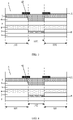
- the present disclosure provides a display substrate which, as shown in FIG. 3 , includes a base 1, and an organic electroluminescent display layer 2, a touch layer 3, a polarizer 4 and a cover plate 5 sequentially stacked on the base 1.
- the organic electroluminescent display layer 2 and the touch layer 3 are bonded with a first bonding layer 6, and the polarizer 4 and the cover plate 5 are bonded with a second bonding layer 7.
- the display substrate includes a display area 101 and a camera installation area 102.
- the display area 101 surrounds the camera installation area 102.
- a camera is configured to be installed on a side of the base 1 away from the organic electroluminescent display layer 2, and located in the camera installation area 102.
- a light-emitting layer is at least not provided in an area of the organic electroluminescent display layer 2 corresponding to the camera installation area 102, and a first opening 41 is provided in an area of the polarizer 4 corresponding to the camera installation area 102.
- the organic electroluminescent display layer 2 includes a pixel driving circuit, an anode, a light-emitting layer and a cathode.
- the light-emitting layer is sandwiched between the anode and the cathode to form a sandwich structure, the anode is connected to the pixel driving circuit, the cathode is connected to a ground terminal, and the light-emitting layer may emit light under driving of the pixel driving circuit to realize display of the display substrate.
- the camera installation area 102 is used for installing a camera.
- each film layer in the display substrate is transparent in the area corresponding to the camera installation area 102, and since the light-emitting layer in the organic electroluminescent display layer 2 may emit light under driving, which may affect shooting of the camera, the light-emitting layer is not disposed in the camera installation area 102, and other film layers of the organic electroluminescent display layer 2 may be disposed or not disposed in the camera installation area 102.
- the light-emitting layer in the organic electroluminescent display layer 2 may emit light during display, it may affect image capture of the camera in the camera installation area 102.
- the polarizer 4 has a large influence on the light transmittance in the display substrate. Therefore, by opening a first opening 41 in an area of the polarizer 4 corresponding to the camera installation area 102, and not providing the light-emitting layer in at least an area of the organic electroluminescent display layer 2 corresponding to the camera installation area 102, shooting light of the camera in the camera installation area 102 of the display substrate can be successfully transmitted, and the requirements of the camera on light transmittance can be met, and thus the camera can capture images normally.
- the opening is provided in only the polarizer 4 in the camera installation area 102 of the display substrate, and the camera is installed on a side of the base 1 away from the organic electroluminescent display layer 2, the camera will not be located in a recessed opening compared with the technology shown in FIG. 1 where each film layer of the display substrate has an opening, thereby avoiding the light scattered and reflected at the edge of the opening and light leakage in the camera installation area 102, and ensuring the shooting effect of the camera. Meanwhile, since the camera is not located in the recessed opening, uneven stress will not occur when the camera is installed in the camera installation area 102, thereby avoiding black spots on the display substrate during display, and ensuring the display effect of the display sub strate.
- the second bonding layer 7 is filled in the first opening 41, and a side surface of the second bonding layer 7 away from the polarizer 4 is flat. With such arrangement, no closed space is formed between the second bonding layer 7 and the cover plate 5 or between the polarizer 4 and the cover plate 5 in the camera installation area 102, and compared with the opening design in the full screen shown in FIG. 2 , poor dents in the camera installation area 102 on the back side of the base 1 of the display substrate during the manufacturing process can be avoided. Since the second bonding layer 7 is made of a transparent bonding adhesive material, the second bonding layer 7 filled in the first opening 41 of the polarizer 4 substantially has no effect on transmittance of the shooting light of the camera.
- the area of the organic electroluminescent display layer 2 corresponding to the camera installation area 102 is provided with a pixel driving circuit 8 disposed on the base 1.
- each film layer (such as a gate, a gate insulation layer, a source, a drain, an active layer, or the like of a transistor) is made of a transparent material, so transmittance of the shooting light of the camera is substantially not affected.
- the first bonding layer 6 is in contact with the pixel driving circuit 8 in the camera installation area 102, and a side surface of the first bonding layer 6 away from the organic electroluminescent display layer 2 is flat. With such arrangement, no closed space is formed between the first bonding layer 6 and the touch layer 3 or between the pixel driving circuit 8 and the touch layer 3 in the camera installation area 102, and compared with the opening design in the full screen shown in FIG. 2 , poor dents in the camera installation area 102 on the back side of the base 1 of the display substrate during the manufacturing process can be avoided. Since the first bonding layer 6 is made of a transparent bonding adhesive material, the first bonding layer 6 substantially has no effect on transmittance of the shooting light of the camera.
- each insulation layer 9 is a transparent organic insulation layer or a transparent inorganic insulation layer extending from the display area 101 of the display substrate to the camera installation area 102.
- Each insulation layer 9 is made of a transparent material, so transmittance of the shooting light of the camera is substantially not affected.
- the first bonding layer 6 is in contact with the insulation layer 9 in the camera installation area 102, and a side surface of the first bonding layer 6 away from the organic electroluminescent display layer 2 is flat. With such arrangement, no closed space is formed between the first bonding layer 6 and the touch layer 3 or between the insulation layers 9 and the touch layer 3 in the camera installation area 102, and compared with the opening design in the full screen shown in FIG. 2 , poor dents in the camera installation area 102 on the back side of the base 1 of the display substrate during the manufacturing process can be avoided. Since the first bonding layer 6 is made of a transparent bonding adhesive material, the first bonding layer 6 substantially has no effect on transmittance of the shooting light of the camera.
- the display substrate further includes an encapsulation layer 10 disposed between the organic electroluminescent display layer 2 and the first bonding layer 6 and configured to encapsulate the organic electroluminescent display layer 2.
- the encapsulation layer 10 may be formed by a laminate of a transparent organic film and a transparent inorganic film. In the camera installation area 102, the encapsulation layer 10 substantially has no effect on transmittance of the shooting light of the camera.
- the cover plate 5 is provided with a light-shielding layer 11 disposed on a side of the cover plate 5 closer to the polarizer 4, and an orthographic projection of the light-shielding layer 11 on the base 1 covers an edge of the camera installation area 102. Due to arrangement of the light-shielding layer 11, light leakage at the edge region of the camera installation area 102 can be shielded, so that light leakage will not occur at the edge region of the camera installation area 102, and thus the display effect of the display substrate and the shooting effect of the camera are ensured.
- the light-shielding layer 11 is made of a black ink material. It should be noted that the light-shielding layer 11 may also be located on a side of the cover plate 5 away from the polarizer 4.
- the base 1, the touch layer 3, and the cover plate 5 are all transparent. Therefore, transmittance of the shooting light of the camera will not be affected in the camera installation area 102.
- the base 1 and the cover plate 5 may both adopt a flexible material to obtain a flexible display substrate.
- the display substrate provided in the above embodiment, by arranging a first opening in an area of the polarizer corresponding to the camera installation area, and not providing the light-emitting layer in at least an area of the organic electroluminescent display layer corresponding to the camera installation area, shooting light of the camera in the camera installation area of the display substrate can be successfully transmitted, and the requirements of the camera on light transmittance can be met, and thus the camera can capture images normally.
- the opening is provided in only the polarizer in the camera installation area of the display substrate, and the camera is installed on a side of the base away from the organic electroluminescent display layer, the camera will not be located in a recessed opening compared with the technology where each film layer of the display substrate has an opening, thereby avoiding the light scattered and reflected at the edge of the opening and light leakage in the camera installation area, and ensuring the shooting effect of the camera.
- the camera since the camera is not located in the recessed opening, uneven stress will not occur when the camera is installed in the camera installation area, thereby avoiding black spots on the display substrate during display, and ensuring the display effect of the display substrate.
- the present disclosure further provides a display apparatus which, as shown in FIG. 6 , includes a display substrate of any of the above embodiments, and further a camera 12 which is disposed on a side of the base 1 away from the organic electroluminescent display layer 2 in the display substrate, and located in the camera installation area 102.
- the display device further includes a heat dissipation layer 13 disposed on the side of the base 1 away from the organic electroluminescent display layer 2 in the display substrate.
- the heat dissipation layer 13 has a second opening 130 provided in an area corresponding to the camera installation area 102 of the display substrate.
- the heat dissipation layer 13 is made of a heat dissipation cotton or a metal heat dissipation material, and the second opening 130 provided in the heat dissipation layer 13 can prevent the heat dissipation layer 13 from blocking the shooting light of the camera 12, thereby ensuring normal shooting of the camera 12.
- the display apparatus further includes a third bonding layer 14 and a fixing plate 15.
- the third bonding layer 14 is disposed in the second opening 130
- the fixing plate 15 is disposed on a side of the third bonding layer 14 away from the base 1, and an orthographic projection of the fixing plate 15 on the base 1 is located in the second opening 130.
- the camera 12 is fixed on the fixing plate 15 and located on a side of the fixing plate 15 away from the display substrate.
- the third bonding layer 14 is made of transparent bonding adhesive.
- the fixing plate 15 is a transparent glass plate.
- the third bonding layer 14 and the fixing plate 15 provided in such manner substantially have no effect on transmittance of the shooting light of the camera 12, and thus will not affect normal shooting of the camera 12.
- a distance between a side surface of the fixing plate 15 away from the base 1 and the base 1 is equal to a thickness of the heat dissipation layer 13.
- the distance between a side surface of the fixing plate 15 away from the base 1 and the base 1 is larger than the thickness of the heat dissipation layer 13.
- the display apparatus provided in the embodiments of the present disclosure, by adopting the display substrate as described above, not only normal shooting of the camera is ensured, but also light leakage in the camera installation area is avoided, thereby ensuring the shooting effect of the camera. Meanwhile, uneven stress will not occur when the camera is installed in the display apparatus, thereby avoiding black spots on the display apparatus during display, and ensuring the display effect of the display apparatus.
- the display apparatus may be any product or component with a display function, such as an OLED panel, an OLED television, a monitor, a mobile phone, a navigator, or the like.
Landscapes
- Inorganic Chemistry (AREA)
- Chemical & Material Sciences (AREA)
- Physics & Mathematics (AREA)
- Engineering & Computer Science (AREA)
- Sustainable Development (AREA)
- Life Sciences & Earth Sciences (AREA)
- Geometry (AREA)
- Microelectronics & Electronic Packaging (AREA)
- Optics & Photonics (AREA)
- Multimedia (AREA)
- Signal Processing (AREA)
- Electroluminescent Light Sources (AREA)
- Devices For Indicating Variable Information By Combining Individual Elements (AREA)
Abstract
Description
- Embodiments of the present disclosure belong to the field of display technology, and specifically relates to a display substrate and a display apparatus.
- At present, implementing a full screen by means of AMOLED (active-matrix organic light-emitting diode) screen modules has gradually become the mainstream, and providing an opening on the full screen for installing a camera is gradually accepted by more and more customers as a full screen scheme.
- Embodiments of the present disclosure provide a display substrate and a display apparatus.
- In a first aspect, an embodiment of the present disclosure provides a display substrate, including a base, and an organic electroluminescent display layer, a touch layer, a polarizer and a cover plate sequentially stacked on the base, where the organic electroluminescent display layer and the touch layer are bonded with a first bonding layer, and the polarizer and the cover plate are bonded with a second bonding layer; the display substrate includes a display area and a camera installation area, the display area surrounds the camera installation area, a camera is configured to be installed on a side of the base away from the organic electroluminescent display layer and located in the camera installation area, a light-emitting layer is at least not provided in an area of the organic electroluminescent display layer corresponding to the camera installation area, and a first opening is provided in an area of the polarizer corresponding to the camera installation area.
- In some embodiments, the second bonding layer is filled in the first opening, and a side surface of the second bonding layer away from the polarizer is flat.
- In some embodiments, the area of the organic electroluminescent display layer corresponding to the camera installation area is provided with a pixel driving circuit disposed on the base.
- In some embodiments, the first bonding layer is in contact with the pixel driving circuit in the camera installation area, and a side surface of the first bonding layer away from the organic electroluminescent display layer is flat.
- In some embodiments, the area of the organic electroluminescent display layer corresponding to the camera installation area is provided with one or more insulation layers disposed on the base.
- In some embodiments, the first bonding layer is in contact with the insulation layer in the camera installation area, and a side surface of the first bonding layer away from the organic electroluminescent display layer is flat.
- In some embodiments, the display substrate further includes an encapsulation layer disposed between the organic electroluminescent display layer and the first bonding layer and configured to encapsulate the organic electroluminescent display layer.
- In some embodiments, the cover plate is provided with a light-shielding layer located on a side of the cover plate closer to the polarizer or away from the polarizer, and an orthographic projection of the light-shielding layer on the base covers an edge of the camera installation area.
- In some embodiments, the base, the touch layer, and the cover plate are all transparent.
- In some embodiments, the first bonding layer and the second bonding layer are both made of a transparent bonding adhesive material.
- In a second aspect, an embodiment of the present disclosure provides a display device, including the display substrate mentioned above and a camera disposed on a side of the base away from the organic electroluminescent display layer in the display substrate, and located in the camera installation area.
- In some embodiments, the display device further includes a heat dissipation layer disposed on the side of the base away from the organic electroluminescent display layer in the display substrate, where the heat dissipation layer includes a second opening provided in an area corresponding to the camera installation area of the display substrate.
- In some embodiments, the display device further includes a third bonding layer and a fixing plate, where the third bonding layer is disposed in the second opening, the fixing plate is disposed on a side of the third bonding layer away from the base, and an orthographic projection of the fixing plate on the base is located in the second opening; and the camera is fixed on the fixing plate and located on a side of the fixing plate away from the display substrate.
- In some embodiments, a distance between a side surface of the fixing plate away from the base and the base is equal to a thickness of the heat dissipation layer.
- In some embodiments, a distance between a side surface of the fixing plate away from the base and the base is larger than the thickness of the heat dissipation layer.
- Accompanying drawings are provided for further understanding of the embodiments of the present disclosure and constitute a part of the specification. Hereinafter, these drawings are intended to explain the present disclosure together with the following embodiments, but should not be considered as a limitation to the present disclosure. The above and other features and advantages will become more apparent to those skilled in the art through detailed description of the exemplary embodiments with reference to the accompanying drawings, in which:
-
FIG. 1 is a schematic sectional view of a design of an opening in an AMOLED full screen in the related art; -
FIG. 2 is a schematic sectional view of another design of an opening in an AMOLED full screen in the related art; -
FIG. 3 is a structural sectional view of a display substrate according to the present disclosure; -
FIG. 4 is a structural sectional view of another display substrate according to the present disclosure; -
FIG. 5 is a structural sectional view of yet another display substrate according to the present disclosure; -
FIG. 6 is a structural sectional view of a display apparatus according to the present disclosure; and -
FIG. 7 is a structural sectional view of another display apparatus according to the present disclosure. - The reference signs therein are listed below:
1. base; 2. organic electroluminescent display layer; 3. touch layer; 4. polarizer; 41. first opening; 5. cover plate; 6. first bonding layer; 7. second bonding layer; 101. display area; 102. camera installation area; 8. pixel driving circuit; 9. insulation layer; 10. encapsulation layer; 11. light-shielding layer; 12. camera; 13. heat dissipation layer; 130. second opening; 14. third bonding layer; and 15. fixing plate. - In order to make those skilled in the art better understand the technical solutions in the embodiments of the present disclosure, the display substrate and the display apparatus provided in the embodiments of the present disclosure are described in further detail below with reference to the accompanying drawings and specific embodiments.
- Embodiments of the present disclosure will be described more sufficiently below with reference to the accompanying drawings, but which may be embodied in different forms and should not be construed as limited to the embodiments set forth in the disclosure. Rather, these embodiments are provided so that this disclosure will be thorough and complete, and will fully convey the scope of the disclosure to those skilled in the art.
- The embodiments of the present disclosure are not limited to the embodiments shown in the drawings, but include modifications of configurations formed based on a manufacturing process. Thus, the areas illustrated in the figures have schematic properties, and the shapes of the areas shown in the figures exemplarily illustrate specific shapes of the areas, but are not intended to be limiting.
-
FIG. 1 is a schematic diagram of a design of an opening in an AMOLED full screen in the related art. Aheat dissipation layer 13, abase 1, an organicelectroluminescent display layer 2, afirst bonding layer 6, atouch layer 3, apolarizer 4 and asecond bonding layer 7 sequentially stacked in the AMOLED full screen, except acover plate 5 disposed on thesecond bonding layer 7, are each provided with an opening in a camera installation position, and acamera 12 is installed in the opening. In this design scheme, light leakage may occur due to light scattered and reflected at an edge of the opening in each film layer, thereby seriously influencing the shooting effect of thecamera 12. Meanwhile, stress on thecamera 12 installed in the openings is uneven, which tends to cause black spots at that position of the display screen during display, and impair the display effect of the display screen. -
FIG. 2 is a schematic diagram of another design of an opening in an AMOLED full screen in the related art. In this scheme, openings are provided only on theheat dissipation layer 13, thepolarizer 4 and thesecond bonding layer 7 at the camera installation position, and thecamera 12 is installed in the opening of theheat dissipation layer 13. In this design scheme, a closed space is formed at the opening positions in thepolarizer 4 and thesecond bonding layer 7, and during high-pressure deaeration in the manufacturing process, a pressure difference between the closed space and the outside may cause poor dents at the camera installation position on the back side of the AMOLED display screen. - Further, in
FIG. 2 , thecamera 12 is installed on thebase 1 exposed in the opening of theheat dissipation layer 13. Since thecamera 12 is located in the recess, light will be scattered and reflected at the edge of the opening of theheat dissipation layer 13, so that the image captured by thecamera 12 may have blurred edges and is not good in the effect. In addition, stress on thecamera 12 installed in the recess is uneven, which tends to cause black spots at that position of the display screen during display, and impair the display effect of the display screen. - Aiming at the problems of light leakage caused by the fact that the camera is installed in the openings of a plurality of stacked film layers of an AMOLED full-face screen, and black spots during display in the related art, the present disclosure discloses a display substrate and a display apparatus.
- The present disclosure provides a display substrate which, as shown in
FIG. 3 , includes abase 1, and an organicelectroluminescent display layer 2, atouch layer 3, apolarizer 4 and acover plate 5 sequentially stacked on thebase 1. The organicelectroluminescent display layer 2 and thetouch layer 3 are bonded with afirst bonding layer 6, and thepolarizer 4 and thecover plate 5 are bonded with asecond bonding layer 7. The display substrate includes adisplay area 101 and acamera installation area 102. Thedisplay area 101 surrounds thecamera installation area 102. A camera is configured to be installed on a side of thebase 1 away from the organicelectroluminescent display layer 2, and located in thecamera installation area 102. A light-emitting layer is at least not provided in an area of the organicelectroluminescent display layer 2 corresponding to thecamera installation area 102, and afirst opening 41 is provided in an area of thepolarizer 4 corresponding to thecamera installation area 102. - The organic
electroluminescent display layer 2 includes a pixel driving circuit, an anode, a light-emitting layer and a cathode. The light-emitting layer is sandwiched between the anode and the cathode to form a sandwich structure, the anode is connected to the pixel driving circuit, the cathode is connected to a ground terminal, and the light-emitting layer may emit light under driving of the pixel driving circuit to realize display of the display substrate. Thecamera installation area 102 is used for installing a camera. In order to ensure that the camera can normally capture images, each film layer in the display substrate is transparent in the area corresponding to thecamera installation area 102, and since the light-emitting layer in the organicelectroluminescent display layer 2 may emit light under driving, which may affect shooting of the camera, the light-emitting layer is not disposed in thecamera installation area 102, and other film layers of the organicelectroluminescent display layer 2 may be disposed or not disposed in thecamera installation area 102. - Since the light-emitting layer in the organic
electroluminescent display layer 2 may emit light during display, it may affect image capture of the camera in thecamera installation area 102. Thepolarizer 4 has a large influence on the light transmittance in the display substrate. Therefore, by opening afirst opening 41 in an area of thepolarizer 4 corresponding to thecamera installation area 102, and not providing the light-emitting layer in at least an area of the organicelectroluminescent display layer 2 corresponding to thecamera installation area 102, shooting light of the camera in thecamera installation area 102 of the display substrate can be successfully transmitted, and the requirements of the camera on light transmittance can be met, and thus the camera can capture images normally. Further, since the opening is provided in only thepolarizer 4 in thecamera installation area 102 of the display substrate, and the camera is installed on a side of thebase 1 away from the organicelectroluminescent display layer 2, the camera will not be located in a recessed opening compared with the technology shown inFIG. 1 where each film layer of the display substrate has an opening, thereby avoiding the light scattered and reflected at the edge of the opening and light leakage in thecamera installation area 102, and ensuring the shooting effect of the camera. Meanwhile, since the camera is not located in the recessed opening, uneven stress will not occur when the camera is installed in thecamera installation area 102, thereby avoiding black spots on the display substrate during display, and ensuring the display effect of the display sub strate. - In the present disclosure, the
second bonding layer 7 is filled in thefirst opening 41, and a side surface of thesecond bonding layer 7 away from thepolarizer 4 is flat. With such arrangement, no closed space is formed between thesecond bonding layer 7 and thecover plate 5 or between thepolarizer 4 and thecover plate 5 in thecamera installation area 102, and compared with the opening design in the full screen shown inFIG. 2 , poor dents in thecamera installation area 102 on the back side of thebase 1 of the display substrate during the manufacturing process can be avoided. Since thesecond bonding layer 7 is made of a transparent bonding adhesive material, thesecond bonding layer 7 filled in thefirst opening 41 of thepolarizer 4 substantially has no effect on transmittance of the shooting light of the camera. - In the present disclosure, the area of the organic
electroluminescent display layer 2 corresponding to thecamera installation area 102 is provided with apixel driving circuit 8 disposed on thebase 1. In thepixel driving circuit 8, each film layer (such as a gate, a gate insulation layer, a source, a drain, an active layer, or the like of a transistor) is made of a transparent material, so transmittance of the shooting light of the camera is substantially not affected. - The
first bonding layer 6 is in contact with thepixel driving circuit 8 in thecamera installation area 102, and a side surface of thefirst bonding layer 6 away from the organicelectroluminescent display layer 2 is flat. With such arrangement, no closed space is formed between thefirst bonding layer 6 and thetouch layer 3 or between thepixel driving circuit 8 and thetouch layer 3 in thecamera installation area 102, and compared with the opening design in the full screen shown inFIG. 2 , poor dents in thecamera installation area 102 on the back side of thebase 1 of the display substrate during the manufacturing process can be avoided. Since thefirst bonding layer 6 is made of a transparent bonding adhesive material, thefirst bonding layer 6 substantially has no effect on transmittance of the shooting light of the camera. - In the present disclosure, as shown in
FIG. 4 , the area of the organicelectroluminescent display layer 2 corresponding to thecamera installation area 102 is provided with one ormore insulation layers 9 disposed on thebase 1. Eachinsulation layer 9 is a transparent organic insulation layer or a transparent inorganic insulation layer extending from thedisplay area 101 of the display substrate to thecamera installation area 102. Eachinsulation layer 9 is made of a transparent material, so transmittance of the shooting light of the camera is substantially not affected. - The
first bonding layer 6 is in contact with theinsulation layer 9 in thecamera installation area 102, and a side surface of thefirst bonding layer 6 away from the organicelectroluminescent display layer 2 is flat. With such arrangement, no closed space is formed between thefirst bonding layer 6 and thetouch layer 3 or between the insulation layers 9 and thetouch layer 3 in thecamera installation area 102, and compared with the opening design in the full screen shown inFIG. 2 , poor dents in thecamera installation area 102 on the back side of thebase 1 of the display substrate during the manufacturing process can be avoided. Since thefirst bonding layer 6 is made of a transparent bonding adhesive material, thefirst bonding layer 6 substantially has no effect on transmittance of the shooting light of the camera. - In the present disclosure, as shown in
FIG. 5 , the display substrate further includes anencapsulation layer 10 disposed between the organicelectroluminescent display layer 2 and thefirst bonding layer 6 and configured to encapsulate the organicelectroluminescent display layer 2. Theencapsulation layer 10 may be formed by a laminate of a transparent organic film and a transparent inorganic film. In thecamera installation area 102, theencapsulation layer 10 substantially has no effect on transmittance of the shooting light of the camera. - In the present disclosure, as shown in
FIG. 3 , thecover plate 5 is provided with a light-shielding layer 11 disposed on a side of thecover plate 5 closer to thepolarizer 4, and an orthographic projection of the light-shielding layer 11 on thebase 1 covers an edge of thecamera installation area 102. Due to arrangement of the light-shielding layer 11, light leakage at the edge region of thecamera installation area 102 can be shielded, so that light leakage will not occur at the edge region of thecamera installation area 102, and thus the display effect of the display substrate and the shooting effect of the camera are ensured. - The light-
shielding layer 11 is made of a black ink material. It should be noted that the light-shielding layer 11 may also be located on a side of thecover plate 5 away from thepolarizer 4. - In the present disclosure, the
base 1, thetouch layer 3, and thecover plate 5 are all transparent. Therefore, transmittance of the shooting light of the camera will not be affected in thecamera installation area 102. Thebase 1 and thecover plate 5 may both adopt a flexible material to obtain a flexible display substrate. - In the display substrate provided in the above embodiment, by arranging a first opening in an area of the polarizer corresponding to the camera installation area, and not providing the light-emitting layer in at least an area of the organic electroluminescent display layer corresponding to the camera installation area, shooting light of the camera in the camera installation area of the display substrate can be successfully transmitted, and the requirements of the camera on light transmittance can be met, and thus the camera can capture images normally. Furthermore, since the opening is provided in only the polarizer in the camera installation area of the display substrate, and the camera is installed on a side of the base away from the organic electroluminescent display layer, the camera will not be located in a recessed opening compared with the technology where each film layer of the display substrate has an opening, thereby avoiding the light scattered and reflected at the edge of the opening and light leakage in the camera installation area, and ensuring the shooting effect of the camera. Meanwhile, since the camera is not located in the recessed opening, uneven stress will not occur when the camera is installed in the camera installation area, thereby avoiding black spots on the display substrate during display, and ensuring the display effect of the display substrate.
- The present disclosure further provides a display apparatus which, as shown in
FIG. 6 , includes a display substrate of any of the above embodiments, and further acamera 12 which is disposed on a side of thebase 1 away from the organicelectroluminescent display layer 2 in the display substrate, and located in thecamera installation area 102. - In the present disclosure, the display device further includes a
heat dissipation layer 13 disposed on the side of thebase 1 away from the organicelectroluminescent display layer 2 in the display substrate. Theheat dissipation layer 13 has asecond opening 130 provided in an area corresponding to thecamera installation area 102 of the display substrate. Theheat dissipation layer 13 is made of a heat dissipation cotton or a metal heat dissipation material, and thesecond opening 130 provided in theheat dissipation layer 13 can prevent theheat dissipation layer 13 from blocking the shooting light of thecamera 12, thereby ensuring normal shooting of thecamera 12. - In the present disclosure, the display apparatus further includes a
third bonding layer 14 and a fixingplate 15. Thethird bonding layer 14 is disposed in thesecond opening 130, the fixingplate 15 is disposed on a side of thethird bonding layer 14 away from thebase 1, and an orthographic projection of the fixingplate 15 on thebase 1 is located in thesecond opening 130. Thecamera 12 is fixed on the fixingplate 15 and located on a side of the fixingplate 15 away from the display substrate. Thethird bonding layer 14 is made of transparent bonding adhesive. The fixingplate 15 is a transparent glass plate. Thethird bonding layer 14 and the fixingplate 15 provided in such manner substantially have no effect on transmittance of the shooting light of thecamera 12, and thus will not affect normal shooting of thecamera 12. - In the present disclosure, a distance between a side surface of the fixing
plate 15 away from thebase 1 and thebase 1 is equal to a thickness of theheat dissipation layer 13. With such arrangement, compared with the camera installation position shown inFIG. 2 , thecamera 12 will not be located in a recessed opening, thereby avoiding the light scattered and reflected at the edge of the opening, as well as blurred edges of the images captured by thecamera 12, and thus ensuring the shooting effect of thecamera 12. Meanwhile, since thecamera 12 is not located in the recessed opening, uneven stress will not occur when thecamera 12 is installed in thecamera installation area 102, thereby avoiding black spots on the display apparatus during display, and ensuring the display effect of the display apparatus. - In the present disclosure, as shown in
FIG. 7 , the distance between a side surface of the fixingplate 15 away from thebase 1 and thebase 1 is larger than the thickness of theheat dissipation layer 13. With such arrangement, compared with the camera installation position shown inFIG. 2 , thecamera 12 will not be located in the recessed opening, thereby avoiding the light scattered and reflected at the edge of the opening, as well as blurred edges of the images captured by thecamera 12, and thus ensuring the shooting effect of thecamera 12. Meanwhile, since thecamera 12 is not located in the recessed opening, uneven stress will not occur when thecamera 12 is installed in thecamera installation area 102, thereby avoiding black spots on the display apparatus during display, and ensuring the display effect of the display apparatus. - In the display apparatus provided in the embodiments of the present disclosure, by adopting the display substrate as described above, not only normal shooting of the camera is ensured, but also light leakage in the camera installation area is avoided, thereby ensuring the shooting effect of the camera. Meanwhile, uneven stress will not occur when the camera is installed in the display apparatus, thereby avoiding black spots on the display apparatus during display, and ensuring the display effect of the display apparatus.
- The display apparatus provided in the embodiments of the present disclosure may be any product or component with a display function, such as an OLED panel, an OLED television, a monitor, a mobile phone, a navigator, or the like.
- It will be appreciated that the above implementations are merely exemplary implementations for the purpose of illustrating the principle of the present disclosure, and the present disclosure is not limited thereto. Various modifications and improvements can be made by a person having ordinary skill in the art without departing from the protection scope of the disclosure defined in the accompany claims, and accordingly, all of these modifications and improvements fall into the protection scope of the present disclosure.
Claims (15)
- A display substrate, comprising a base, and an organic electroluminescent display layer, a touch layer, a polarizer and a cover plate sequentially stacked on the base,wherein the organic electroluminescent display layer and the touch layer are bonded with a first bonding layer, and the polarizer and the cover plate are bonded with a second bonding layer,wherein the display substrate comprises a display area and a camera installation area, the display area surrounds the camera installation area, a camera is configured to be installed on a side of the base away from the organic electroluminescent display layer and located in the camera installation area, andwherein a light-emitting layer is at least not provided in an area of the organic electroluminescent display layer corresponding to the camera installation area, and a first opening is provided in an area of the polarizer corresponding to the camera installation area.
- The display substrate according to claim 1, wherein the second bonding layer is filled in the first opening, and a side surface of the second bonding layer away from the polarizer is flat.
- The display substrate according to claim 1, wherein the area of the organic electroluminescent display layer corresponding to the camera installation area is provided with a pixel driving circuit disposed on the base.
- The display substrate according to claim 3, wherein the first bonding layer is in contact with the pixel driving circuit in the camera installation area, and a side surface of the first bonding layer away from the organic electroluminescent display layer is flat.
- The display substrate according to claim 1, wherein the area of the organic electroluminescent display layer corresponding to the camera installation area is provided with one or more insulation layers disposed on the base.
- The display substrate according to claim 5, wherein the first bonding layer is in contact with the one or more insulation layers in the camera installation area, and a side surface of the first bonding layer away from the organic electroluminescent display layer is flat.
- The display substrate according to claim 1, further comprising an encapsulation layer disposed between the organic electroluminescent display layer and the first bonding layer and configured to encapsulate the organic electroluminescent display layer.
- The display substrate according to claim 1, wherein the cover plate is provided with a light-shielding layer located on a side of the cover plate closer to the polarizer or away from the polarizer, and an orthographic projection of the light-shielding layer on the base covers an edge of the camera installation area.
- The display substrate according to claim 1, wherein the base, the touch layer, and the cover plate are all transparent.
- The display substrate according to claim 1, wherein the first bonding layer and the second bonding layer are both made of a transparent bonding adhesive material.
- A display device, comprising the display substrate according to any one of claims 1 to 10, and further comprising a camera which is disposed on a side of the base away from the organic electroluminescent display layer in the display substrate, and located in the camera installation area.
- The display apparatus according to claim 11, further comprising a heat dissipation layer disposed on a side of the base away from the organic electroluminescent display layer in the display substrate,
wherein the heat dissipation layer has a second opening provided in an area corresponding to the camera installation area of the display substrate. - The display apparatus according to claim 12, further comprising a third bonding layer and a fixing plate,wherein the third bonding layer is disposed in the second opening, the fixing plate is disposed on a side of the third bonding layer away from the base, and an orthographic projection of the fixing plate on the base is located in the second opening, andwherein the camera is fixed on the fixing plate and located on a side of the fixing plate away from the display substrate.
- The display apparatus according to claim 13, wherein a distance between a side surface of the fixing plate away from the base and the base is equal to a thickness of the heat dissipation layer.
- The display apparatus according to claim 13, wherein a distance between a side surface of the fixing plate away from the base and the base is larger than a thickness of the heat dissipation layer.
Applications Claiming Priority (2)
| Application Number | Priority Date | Filing Date | Title |
|---|---|---|---|
| CN202020646909.5U CN211743161U (en) | 2020-04-24 | 2020-04-24 | Display substrate and display device |
| PCT/CN2021/080011 WO2021213049A1 (en) | 2020-04-24 | 2021-03-10 | Display substrate and display apparatus |
Publications (2)
| Publication Number | Publication Date |
|---|---|
| EP4036980A1 true EP4036980A1 (en) | 2022-08-03 |
| EP4036980A4 EP4036980A4 (en) | 2023-01-04 |
Family
ID=72852343
Family Applications (1)
| Application Number | Title | Priority Date | Filing Date |
|---|---|---|---|
| EP21792331.7A Pending EP4036980A4 (en) | 2020-04-24 | 2021-03-10 | DISPLAY SUBSTRATE AND DISPLAY APPARATUS |
Country Status (6)
| Country | Link |
|---|---|
| US (1) | US12336387B2 (en) |
| EP (1) | EP4036980A4 (en) |
| JP (1) | JP7697942B2 (en) |
| KR (1) | KR102950046B1 (en) |
| CN (1) | CN211743161U (en) |
| WO (1) | WO2021213049A1 (en) |
Families Citing this family (8)
| Publication number | Priority date | Publication date | Assignee | Title |
|---|---|---|---|---|
| CN211743161U (en) * | 2020-04-24 | 2020-10-23 | 京东方科技集团股份有限公司 | Display substrate and display device |
| CN114694483B (en) * | 2020-12-25 | 2025-12-19 | 京东方科技集团股份有限公司 | Display module and display device |
| CN113035913B (en) * | 2021-02-26 | 2022-10-04 | 武汉华星光电半导体显示技术有限公司 | Preparation method of display panel, display panel and display device |
| CN113035928B (en) * | 2021-03-10 | 2024-09-20 | 京东方科技集团股份有限公司 | Display substrate, display panel and manufacturing method thereof |
| CN114464753B (en) * | 2022-01-19 | 2023-10-31 | 武汉华星光电半导体显示技术有限公司 | Display panel and cover plate assembly |
| CN114627764A (en) * | 2022-03-16 | 2022-06-14 | 武汉华星光电半导体显示技术有限公司 | Display module and display device |
| WO2024044945A1 (en) * | 2022-08-30 | 2024-03-07 | 京东方科技集团股份有限公司 | Assembly member for display module, display module, and tiled display device |
| CN115996595B (en) * | 2023-01-13 | 2026-01-27 | 昆山国显光电有限公司 | Display panel and display device |
Family Cites Families (18)
| Publication number | Priority date | Publication date | Assignee | Title |
|---|---|---|---|---|
| KR20170111827A (en) * | 2016-03-29 | 2017-10-12 | 삼성전자주식회사 | Electronic device including display and camera |
| WO2018216545A1 (en) * | 2017-05-22 | 2018-11-29 | シャープ株式会社 | Display device |
| CN107359185B (en) * | 2017-07-27 | 2021-05-14 | 京东方科技集团股份有限公司 | A display panel and display device |
| WO2019047126A1 (en) * | 2017-09-07 | 2019-03-14 | 华为技术有限公司 | Organic light-emitting display (oled) screen and terminal |
| CN107946341B (en) * | 2017-11-10 | 2020-05-22 | 上海天马微电子有限公司 | Display device and method for manufacturing display device |
| KR102572136B1 (en) | 2018-01-08 | 2023-08-29 | 삼성디스플레이 주식회사 | Electroluminescent device having window |
| KR102443229B1 (en) * | 2018-01-23 | 2022-09-15 | 삼성전자주식회사 | A display comprising an opening for mounting a sensor |
| CN208433994U (en) * | 2018-04-26 | 2019-01-25 | Oppo广东移动通信有限公司 | Terminal display assembly and mobile terminal |
| KR102485901B1 (en) * | 2018-06-12 | 2023-01-09 | 삼성전자주식회사 | Electronic device including sensor and manufacuturing method thereof |
| CN109817678A (en) | 2019-01-30 | 2019-05-28 | 武汉华星光电半导体显示技术有限公司 | Display panel and display device |
| CN209881831U (en) * | 2019-03-28 | 2019-12-31 | 宁波舜宇光电信息有限公司 | Terminal device and display unit thereof |
| CN111863868B (en) * | 2019-04-25 | 2023-01-13 | 宁波舜宇光电信息有限公司 | Under-screen camera shooting assembly, corresponding organic light emitting diode display screen and terminal equipment |
| CN110233167B (en) | 2019-06-18 | 2021-12-03 | 京东方科技集团股份有限公司 | Display panel, display device and manufacturing method of display panel |
| CN110335890A (en) * | 2019-07-11 | 2019-10-15 | 京东方科技集团股份有限公司 | A kind of display panel and preparation method thereof, display device |
| CN110491909B (en) * | 2019-07-29 | 2021-12-24 | 武汉华星光电技术有限公司 | Display panel |
| CN110600511A (en) * | 2019-08-26 | 2019-12-20 | 武汉华星光电半导体显示技术有限公司 | Organic light emitting display panel and method of manufacturing the same |
| CN110610970A (en) | 2019-08-29 | 2019-12-24 | 武汉华星光电半导体显示技术有限公司 | Display panel, display device and display panel preparation method |
| CN211743161U (en) | 2020-04-24 | 2020-10-23 | 京东方科技集团股份有限公司 | Display substrate and display device |
-
2020
- 2020-04-24 CN CN202020646909.5U patent/CN211743161U/en active Active
-
2021
- 2021-03-10 JP JP2022523993A patent/JP7697942B2/en active Active
- 2021-03-10 KR KR1020227017293A patent/KR102950046B1/en active Active
- 2021-03-10 WO PCT/CN2021/080011 patent/WO2021213049A1/en not_active Ceased
- 2021-03-10 US US17/635,749 patent/US12336387B2/en active Active
- 2021-03-10 EP EP21792331.7A patent/EP4036980A4/en active Pending
Also Published As
| Publication number | Publication date |
|---|---|
| CN211743161U (en) | 2020-10-23 |
| KR102950046B1 (en) | 2026-04-08 |
| JP2023522508A (en) | 2023-05-31 |
| US12336387B2 (en) | 2025-06-17 |
| WO2021213049A1 (en) | 2021-10-28 |
| JP7697942B2 (en) | 2025-06-24 |
| KR20230002264A (en) | 2023-01-05 |
| EP4036980A4 (en) | 2023-01-04 |
| US20220344426A1 (en) | 2022-10-27 |
Similar Documents
| Publication | Publication Date | Title |
|---|---|---|
| US12336387B2 (en) | Display substrate and display apparatus | |
| CN110853507B (en) | Display screen and electronic equipment | |
| KR102746592B1 (en) | Display device | |
| KR102745476B1 (en) | Display Device and Method for Manufacturing the Same | |
| US20200186688A1 (en) | Display panel and display device using same | |
| US9990001B2 (en) | Electronic device display structures | |
| US8319419B2 (en) | Organic EL display apparatus | |
| US9935159B2 (en) | Display panel and display device comprising the same | |
| US10522602B1 (en) | Organic light-emitting display panel and display device | |
| CN110879493B (en) | Display panel and display device | |
| US20170221974A1 (en) | Display device | |
| US20110199549A1 (en) | Display device and electronic apparatus | |
| CN105700229A (en) | Backlight unit and liquid crystal display device including the same | |
| JP2019095505A (en) | Display device | |
| CN110955079A (en) | Liquid crystal display device having a plurality of pixel electrodes | |
| US20200174307A1 (en) | Liquid crystal display device having high screen ratio | |
| CN110796954A (en) | Display module, manufacturing method thereof and display device | |
| CN111371927B (en) | Display Backplanes, Displays and Electronics | |
| CN115835718A (en) | display device | |
| CN113013219A (en) | Display device | |
| US12527204B2 (en) | Terminal apparatus, display panel with light-shielding body filled in mounting hole, and manufacturing method thereof | |
| KR101504595B1 (en) | Display panel, display panel module and electronic apparatus | |
| KR20150078184A (en) | Flexible display device and method of fabricating the same | |
| CN117082895B (en) | Display panel, its manufacturing method and display device | |
| KR20150017286A (en) | Flexible organic light emitting diode display device and method of fabricating the same |
Legal Events
| Date | Code | Title | Description |
|---|---|---|---|
| STAA | Information on the status of an ep patent application or granted ep patent |
Free format text: STATUS: THE INTERNATIONAL PUBLICATION HAS BEEN MADE |
|
| PUAI | Public reference made under article 153(3) epc to a published international application that has entered the european phase |
Free format text: ORIGINAL CODE: 0009012 |
|
| STAA | Information on the status of an ep patent application or granted ep patent |
Free format text: STATUS: REQUEST FOR EXAMINATION WAS MADE |
|
| 17P | Request for examination filed |
Effective date: 20220425 |
|
| AK | Designated contracting states |
Kind code of ref document: A1 Designated state(s): AL AT BE BG CH CY CZ DE DK EE ES FI FR GB GR HR HU IE IS IT LI LT LU LV MC MK MT NL NO PL PT RO RS SE SI SK SM TR |
|
| A4 | Supplementary search report drawn up and despatched |
Effective date: 20221202 |
|
| RIC1 | Information provided on ipc code assigned before grant |
Ipc: H01L 51/52 20060101ALI20221128BHEP Ipc: H01L 27/32 20060101AFI20221128BHEP |
|
| DAV | Request for validation of the european patent (deleted) | ||
| DAX | Request for extension of the european patent (deleted) | ||
| P01 | Opt-out of the competence of the unified patent court (upc) registered |
Effective date: 20230706 |
|
| STAA | Information on the status of an ep patent application or granted ep patent |
Free format text: STATUS: EXAMINATION IS IN PROGRESS |
|
| 17Q | First examination report despatched |
Effective date: 20240604 |