EP4036968A1 - Packaged electronic system formed by electrically connected and galvanically isolated dice - Google Patents
Packaged electronic system formed by electrically connected and galvanically isolated dice Download PDFInfo
- Publication number
- EP4036968A1 EP4036968A1 EP22153019.9A EP22153019A EP4036968A1 EP 4036968 A1 EP4036968 A1 EP 4036968A1 EP 22153019 A EP22153019 A EP 22153019A EP 4036968 A1 EP4036968 A1 EP 4036968A1
- Authority
- EP
- European Patent Office
- Prior art keywords
- region
- buried conductive
- die
- support
- conductive region
- Prior art date
- Legal status (The legal status is an assumption and is not a legal conclusion. Google has not performed a legal analysis and makes no representation as to the accuracy of the status listed.)
- Granted
Links
Images



Classifications
-
- H—ELECTRICITY
- H10—SEMICONDUCTOR DEVICES; ELECTRIC SOLID-STATE DEVICES NOT OTHERWISE PROVIDED FOR
- H10W—GENERIC PACKAGES, INTERCONNECTIONS, CONNECTORS OR OTHER CONSTRUCTIONAL DETAILS OF DEVICES COVERED BY CLASS H10
- H10W44/00—Electrical arrangements for controlling or matching impedance
- H10W44/601—Capacitive arrangements
-
- H—ELECTRICITY
- H10—SEMICONDUCTOR DEVICES; ELECTRIC SOLID-STATE DEVICES NOT OTHERWISE PROVIDED FOR
- H10W—GENERIC PACKAGES, INTERCONNECTIONS, CONNECTORS OR OTHER CONSTRUCTIONAL DETAILS OF DEVICES COVERED BY CLASS H10
- H10W70/00—Package substrates; Interposers; Redistribution layers [RDL]
- H10W70/40—Leadframes
- H10W70/411—Chip-supporting parts, e.g. die pads
- H10W70/415—Leadframe inner leads serving as die pads
-
- H—ELECTRICITY
- H10—SEMICONDUCTOR DEVICES; ELECTRIC SOLID-STATE DEVICES NOT OTHERWISE PROVIDED FOR
- H10W—GENERIC PACKAGES, INTERCONNECTIONS, CONNECTORS OR OTHER CONSTRUCTIONAL DETAILS OF DEVICES COVERED BY CLASS H10
- H10W70/00—Package substrates; Interposers; Redistribution layers [RDL]
- H10W70/40—Leadframes
- H10W70/421—Shapes or dispositions
- H10W70/435—Shapes or dispositions of insulating layers on leadframes, e.g. bridging members
-
- H—ELECTRICITY
- H10—SEMICONDUCTOR DEVICES; ELECTRIC SOLID-STATE DEVICES NOT OTHERWISE PROVIDED FOR
- H10W—GENERIC PACKAGES, INTERCONNECTIONS, CONNECTORS OR OTHER CONSTRUCTIONAL DETAILS OF DEVICES COVERED BY CLASS H10
- H10W70/00—Package substrates; Interposers; Redistribution layers [RDL]
- H10W70/40—Leadframes
- H10W70/464—Additional interconnections in combination with leadframes
- H10W70/468—Circuit boards
-
- H—ELECTRICITY
- H10—SEMICONDUCTOR DEVICES; ELECTRIC SOLID-STATE DEVICES NOT OTHERWISE PROVIDED FOR
- H10W—GENERIC PACKAGES, INTERCONNECTIONS, CONNECTORS OR OTHER CONSTRUCTIONAL DETAILS OF DEVICES COVERED BY CLASS H10
- H10W70/00—Package substrates; Interposers; Redistribution layers [RDL]
- H10W70/60—Insulating or insulated package substrates; Interposers; Redistribution layers
- H10W70/611—Insulating or insulated package substrates; Interposers; Redistribution layers for connecting multiple chips together
-
- H—ELECTRICITY
- H10—SEMICONDUCTOR DEVICES; ELECTRIC SOLID-STATE DEVICES NOT OTHERWISE PROVIDED FOR
- H10W—GENERIC PACKAGES, INTERCONNECTIONS, CONNECTORS OR OTHER CONSTRUCTIONAL DETAILS OF DEVICES COVERED BY CLASS H10
- H10W70/00—Package substrates; Interposers; Redistribution layers [RDL]
- H10W70/60—Insulating or insulated package substrates; Interposers; Redistribution layers
- H10W70/62—Insulating or insulated package substrates; Interposers; Redistribution layers characterised by their interconnections
- H10W70/63—Vias, e.g. via plugs
- H10W70/635—Through-vias
-
- H—ELECTRICITY
- H10—SEMICONDUCTOR DEVICES; ELECTRIC SOLID-STATE DEVICES NOT OTHERWISE PROVIDED FOR
- H10W—GENERIC PACKAGES, INTERCONNECTIONS, CONNECTORS OR OTHER CONSTRUCTIONAL DETAILS OF DEVICES COVERED BY CLASS H10
- H10W70/00—Package substrates; Interposers; Redistribution layers [RDL]
- H10W70/60—Insulating or insulated package substrates; Interposers; Redistribution layers
- H10W70/62—Insulating or insulated package substrates; Interposers; Redistribution layers characterised by their interconnections
- H10W70/65—Shapes or dispositions of interconnections
-
- H—ELECTRICITY
- H10—SEMICONDUCTOR DEVICES; ELECTRIC SOLID-STATE DEVICES NOT OTHERWISE PROVIDED FOR
- H10W—GENERIC PACKAGES, INTERCONNECTIONS, CONNECTORS OR OTHER CONSTRUCTIONAL DETAILS OF DEVICES COVERED BY CLASS H10
- H10W70/00—Package substrates; Interposers; Redistribution layers [RDL]
- H10W70/60—Insulating or insulated package substrates; Interposers; Redistribution layers
- H10W70/67—Insulating or insulated package substrates; Interposers; Redistribution layers characterised by their insulating layers or insulating parts
- H10W70/68—Shapes or dispositions thereof
- H10W70/685—Shapes or dispositions thereof comprising multiple insulating layers
-
- H—ELECTRICITY
- H10—SEMICONDUCTOR DEVICES; ELECTRIC SOLID-STATE DEVICES NOT OTHERWISE PROVIDED FOR
- H10W—GENERIC PACKAGES, INTERCONNECTIONS, CONNECTORS OR OTHER CONSTRUCTIONAL DETAILS OF DEVICES COVERED BY CLASS H10
- H10W72/00—Interconnections or connectors in packages
-
- H—ELECTRICITY
- H10—SEMICONDUCTOR DEVICES; ELECTRIC SOLID-STATE DEVICES NOT OTHERWISE PROVIDED FOR
- H10W—GENERIC PACKAGES, INTERCONNECTIONS, CONNECTORS OR OTHER CONSTRUCTIONAL DETAILS OF DEVICES COVERED BY CLASS H10
- H10W72/00—Interconnections or connectors in packages
- H10W72/20—Bump connectors, e.g. solder bumps or copper pillars; Dummy bumps; Thermal bumps
-
- H—ELECTRICITY
- H10—SEMICONDUCTOR DEVICES; ELECTRIC SOLID-STATE DEVICES NOT OTHERWISE PROVIDED FOR
- H10W—GENERIC PACKAGES, INTERCONNECTIONS, CONNECTORS OR OTHER CONSTRUCTIONAL DETAILS OF DEVICES COVERED BY CLASS H10
- H10W74/00—Encapsulations, e.g. protective coatings
- H10W74/10—Encapsulations, e.g. protective coatings characterised by their shape or disposition
- H10W74/111—Encapsulations, e.g. protective coatings characterised by their shape or disposition the semiconductor body being completely enclosed
-
- H—ELECTRICITY
- H10—SEMICONDUCTOR DEVICES; ELECTRIC SOLID-STATE DEVICES NOT OTHERWISE PROVIDED FOR
- H10W—GENERIC PACKAGES, INTERCONNECTIONS, CONNECTORS OR OTHER CONSTRUCTIONAL DETAILS OF DEVICES COVERED BY CLASS H10
- H10W90/00—Package configurations
-
- H—ELECTRICITY
- H10—SEMICONDUCTOR DEVICES; ELECTRIC SOLID-STATE DEVICES NOT OTHERWISE PROVIDED FOR
- H10W—GENERIC PACKAGES, INTERCONNECTIONS, CONNECTORS OR OTHER CONSTRUCTIONAL DETAILS OF DEVICES COVERED BY CLASS H10
- H10W90/00—Package configurations
- H10W90/811—Multiple chips on leadframes
-
- H—ELECTRICITY
- H10—SEMICONDUCTOR DEVICES; ELECTRIC SOLID-STATE DEVICES NOT OTHERWISE PROVIDED FOR
- H10W—GENERIC PACKAGES, INTERCONNECTIONS, CONNECTORS OR OTHER CONSTRUCTIONAL DETAILS OF DEVICES COVERED BY CLASS H10
- H10W72/00—Interconnections or connectors in packages
- H10W72/20—Bump connectors, e.g. solder bumps or copper pillars; Dummy bumps; Thermal bumps
- H10W72/29—Bond pads specially adapted therefor
-
- H—ELECTRICITY
- H10—SEMICONDUCTOR DEVICES; ELECTRIC SOLID-STATE DEVICES NOT OTHERWISE PROVIDED FOR
- H10W—GENERIC PACKAGES, INTERCONNECTIONS, CONNECTORS OR OTHER CONSTRUCTIONAL DETAILS OF DEVICES COVERED BY CLASS H10
- H10W72/00—Interconnections or connectors in packages
- H10W72/851—Dispositions of multiple connectors or interconnections
- H10W72/874—On different surfaces
- H10W72/877—Bump connectors and die-attach connectors
-
- H—ELECTRICITY
- H10—SEMICONDUCTOR DEVICES; ELECTRIC SOLID-STATE DEVICES NOT OTHERWISE PROVIDED FOR
- H10W—GENERIC PACKAGES, INTERCONNECTIONS, CONNECTORS OR OTHER CONSTRUCTIONAL DETAILS OF DEVICES COVERED BY CLASS H10
- H10W90/00—Package configurations
- H10W90/701—Package configurations characterised by the relative positions of pads or connectors relative to package parts
-
- H—ELECTRICITY
- H10—SEMICONDUCTOR DEVICES; ELECTRIC SOLID-STATE DEVICES NOT OTHERWISE PROVIDED FOR
- H10W—GENERIC PACKAGES, INTERCONNECTIONS, CONNECTORS OR OTHER CONSTRUCTIONAL DETAILS OF DEVICES COVERED BY CLASS H10
- H10W90/00—Package configurations
- H10W90/701—Package configurations characterised by the relative positions of pads or connectors relative to package parts
- H10W90/721—Package configurations characterised by the relative positions of pads or connectors relative to package parts of bump connectors
- H10W90/724—Package configurations characterised by the relative positions of pads or connectors relative to package parts of bump connectors between a chip and a stacked insulating package substrate, interposer or RDL
-
- H—ELECTRICITY
- H10—SEMICONDUCTOR DEVICES; ELECTRIC SOLID-STATE DEVICES NOT OTHERWISE PROVIDED FOR
- H10W—GENERIC PACKAGES, INTERCONNECTIONS, CONNECTORS OR OTHER CONSTRUCTIONAL DETAILS OF DEVICES COVERED BY CLASS H10
- H10W90/00—Package configurations
- H10W90/701—Package configurations characterised by the relative positions of pads or connectors relative to package parts
- H10W90/721—Package configurations characterised by the relative positions of pads or connectors relative to package parts of bump connectors
- H10W90/728—Package configurations characterised by the relative positions of pads or connectors relative to package parts of bump connectors between a chip and a stacked discrete passive device, e.g. resistors, capacitors or inductors
-
- H—ELECTRICITY
- H10—SEMICONDUCTOR DEVICES; ELECTRIC SOLID-STATE DEVICES NOT OTHERWISE PROVIDED FOR
- H10W—GENERIC PACKAGES, INTERCONNECTIONS, CONNECTORS OR OTHER CONSTRUCTIONAL DETAILS OF DEVICES COVERED BY CLASS H10
- H10W90/00—Package configurations
- H10W90/701—Package configurations characterised by the relative positions of pads or connectors relative to package parts
- H10W90/731—Package configurations characterised by the relative positions of pads or connectors relative to package parts of die-attach connectors
- H10W90/736—Package configurations characterised by the relative positions of pads or connectors relative to package parts of die-attach connectors between a chip and a stacked lead frame, conducting package substrate or heat sink
Definitions
- the present invention relates to a packaged electronic system formed by electrically connected and galvanically isolated dice.
- the invention relates to an electronic system where the dice are packaged in a same package and integrate electronic devices (components and/or circuits) configured to work at very different voltages and to exchange signals with each other.
- the electronic system may be a power-supply system, a digital isolator, a power transistor driving system, a DC-DC converter, or other system where at least one of the devices operates at high voltage (even higher than 10 kV) and/or high power.
- packages dedicated to providing a high isolation level are mainly based upon two approaches:
- a package 5 of resin or other insulating material encloses a system comprising two dice 8, 9 integrating a respective electronic circuit 10 and a respective isolation element 11.
- the circuits 10 may be ASICs (Application-Specific Integrated Circuits); alternatively, one or both circuits 10 may integrate individual electronic components and/or be formed by different circuits.
- the circuits 10 are connected to the respective isolation elements 11 through buried or surface connections, not shown; the isolation elements 11 in the dice 8, 9 are connected by connection wires 12.
- the dice 8, 9 are each fixed to a respective supporting element 15 that is part of a leadframe for connecting different terminals of the circuits 10 to the outside, in a per se known manner.
- Bonding wires 16 connect the terminals of the circuits 10 to the respective leadframe 15, and the package 5 embeds the dice 8, 9, the wires 12, 16 and part of the leadframe 15 so as to electrically isolate them and protect them from the external environment.
- connection wires 12 are just a few, are short, and are arranged in a less critical position (downstream of the isolation elements 11), but, in some applications, may be far from flexible.
- the designer has only a few degrees of freedom in the design of the isolation elements, being constrained to the technologies and platforms for manufacturing the circuits 10.
- the designer is not always able to use the most advanced approaches and knowledge and frequently cannot use the same isolation elements when the circuits 10 of the dice 8, 9 are manufactured using different technologies.
- a package 25 of resin or other insulating material encloses a system formed by two "operative" dice (first and second die 28, 29).
- the dice 28, 29 integrate each an electronic circuit or component 26 and 27, respectively, and are fixed to a respective leadframe 22, 23, also here shown in a simplified way.
- the isolation element, designated by 31, is integrated in a third die 32 fixed on one of the two leadframes, here on the leadframe 22 carrying the first die 28.
- the first circuit 26 is connected to the isolation element 31 through first connection wires 35
- the second circuit 27 is connected to the isolation element 31 through second connection wires 36, generally longer than the first connection wires 35.
- Bonding wires 38 connect the terminals of the circuits 26, 27 to the respective leadframes 22, 23, and the package 25 embeds the dice 28, 29, 32, the wires 35, 36, 38, and part of the leadframes 22, 23.
- the three-dice approach is very flexible and enables use of isolation optimized platforms, irrespective of the technology used for the circuits 26, 27.
- this approach has parasitic components due to the first connection wires 35 and, in particular, the second connection wires 36, which can cause problems of cross-talk, i.e., interference between the signal-transmission channels.
- US 2013/0168854 discloses a semiconductor package having a bridge interposer accommodating routing traces connected to signal pads formed by a surface of the bridge interposer.
- WO 97/24740 describes an inter-chip connections including a wafer accommodating a conductive path physically connected to capacitor plates on the surface of the assembly through wire lines etched in the wafer.
- Aim of the present invention is to provide a solution that overcomes the drawbacks of the prior art.
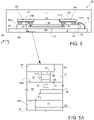
- Figure 5 shows a system 50 comprising two dice 51, 52 integrating each an own device 53, 54.
- the devices 53, 54 are here both ASICs, as indicated above.
- the dice 51, 52 are both fixed to a support 55.
- the support 55 has, for example, a parallelepipedal shape having a first and a second main face 55A, 55B (see also the detail of Figure 5A ).
- the two main faces 55A, 55B here extend parallel to a plane XY of a Cartesian coordinate system XYZ; the support moreover has a height (parallel to a third axis Z of the Cartesian coordinate system XYZ) that is smaller than the width and length (parallel to a first axis X and a second axis Y, respectively, of the Cartesian coordinate system XYZ).
- the support 55 is an organic support, generally of insulating material, housing inside it a buried conductive region 56.
- the buried conductive region 56 is completely surrounded by the insulating material of the support 55 so that there are no physical conductive connection paths with other parts of the system 50 (in other words, the buried conductive region 56 is floating).
- the support 55 may be formed by a printed-circuit board.
- the support 55 is formed by a multilayer including a sequence of conductive layers, typically of metal, and by insulating layers, for example of organic plastic, and one of the conductive layers forms the buried conductive region 56, as described more fully hereinafter with reference to Figure 6 .
- the buried conductive region 56 is planar, and extends as far as underneath the dice 51, 52.
- the buried conductive region 56 extends for most of the length of the support 55 (parallel to the first axis X).
- Contact structures 57A-57D extend on the first face 55A of support 55 for electrical connection of dice 51, 52.
- the contact structures 57A-57D are here formed by a bottom portion 65, for example formed by a support pad region, arranged on the first face 55A of the support 55; an intermediate portion 66, forming a bump region, here arranged on the bottom portion 65; and a top portion 67, for example formed by a die pad region, here arranged on the intermediate portion 66 and formed, from example, by respective top metal layers of the dice 51, 52, in a per se known manner.
- top portions 67 of the contact structures 57A-57D are electrically connected to the electrical components of the devices 53, 54, in a known way.
- first and second contact structures 57A, 57B connect the first die 51 to the support 55
- third and fourth contact structures 57C, 57D connect the second die 52 to the support 55.
- the bottom portions 65 of the second and third contact structures 57B, 57C extend vertically on a respective longitudinal end of the buried conductive region 56 and are thus capacitively coupled thereto. Consequently, in this embodiment, the bottom portions 65 of the second and third contact structures 57B, 57C form first plates of capacitive elements having a common counterplate formed by the buried conductive region 56. In this embodiment, then, the bottom portions 65 are also referred to as first plates 65, and the buried conductive region 56 is also referred to as common floating plate 56.
- the buried conductive region 56 is a planar structure comprising portions arranged below, and capacitively coupled with, the first plates 65.
- a first capacitor 70 is formed between the second contact structure 57B and the buried conductive region 56
- a second capacitor 71 is formed between the third contact structure 57C and the buried conductive region 56.
- the first and second capacitors 70, 71 are arranged in series to each other through the buried conductive region 56, thereby providing a galvanic-coupling structure 73 between the first and second dice 51, 52, as discussed in detail hereinafter.
- the first and fourth contact structures 57A, 57D (as well as other possible contact structures, not shown) connect the respective dice 51, 52 electrically to further support pad regions on the support 55, in a way not shown and known to the person skilled in the art.
- a first and a second external connection region 60, 61 are fixed to the second main face 55B of the support 55.
- the external connection regions 60, 61 here implement an LGA (Land Grid Array) connection scheme and form part, in a known way, of a leadframe formed by distinct external connection regions, electrically isolated from each other, which enable electrical connection of the system 50 to the outside.
- the shown external connection regions 60, 61 are configured so as to be able to work at voltages very different from each other and/or from operating voltages of one or both of the devices 53, 54, even up to 10 kV.
- the external connection regions 60, 61 extend at a distance D1 and, in this embodiment, are fixed to the support 55 so as not to vertically overlap the buried conductive region 56.
- a further pad region 75 extends on the first face 55A of the support 55.
- the further pad region 75 may be provided in the same layer as the first plates 65, in a way known to the person skilled in the art, and is connected to the second external connection region 61 by an electrical connection wire 76.
- a packaging mass 77 of resin or other insulating material, encloses the dice 51, 52, the support 55, the electrical connection wire 76, and a most of the external connection regions 60, 61.
- the capacitors 70, 71 provide a galvanic transmission channel between the devices 53, 54, that enables transmission of common mode signals between the devices 53, 54.
- This channel can be used as single transmission channel, according to the devices 53, 54, the specific exchanged signals, and the design choices.
- the system 50 may include a plurality of such channels, each for a respective signal to be exchanged and/or a transmission direction, as discussed in detail hereinafter.
- the distance D2 between the external connection regions 60, 61 is chosen to be greater than the distance D1 between the dice 51, 52.
- T1 may be higher than T2 (T1 > T2). In general, T1 ⁇ T2.
- Figure 6 shows a possible implementation of the support 55.
- the support 55 of Figure 6 is manufactured starting from a board of a commercially available type, formed by a multilayer.
- the support 55 comprises a bottom insulating layer 80; a bottom conductive layer 81, overlying the bottom insulating layer 80; an intermediate insulating layer 82, the so called core, overlying the bottom insulating layer 80 and the bottom conductive layer 81; a top conductive layer 83, overlying the intermediate insulating layer 82; a top insulating layer 84, overlying the intermediate insulating layer 82 and the top conductive layer 83; and a top conductive layer 85, overlying the top insulating layer 84.
- the insulating layers 80, 82, 84 may be of organic material, for example plastic, such as so-called insulating prepeg; the conductive layers 81, 83 and 85 may be of metal, such as copper. Possibly, the top conductive layer 83 may further comprise a layer with very low contact resistance, for example a gold-based layer, overlying the copper layer.
- the conductive layers 81, 83 and 85 are shaped to form, respectively, the buried conductive region 56, the top plate regions 88 of the capacitors 70, 71, and the bottom portions 65 of the second and third contact structures 57B, 57C.
- the support 55 may comprise a bottom conductive layer, arranged underneath the bottom insulating layer 80 and also of metal, such as copper, possibly coated with a gold-based layer (see also the description of Figure 12 ) .
- the capacitors 70, 71 are formed by the bottom conductive layer 81 (buried conductive region 56), the intermediate insulating layer 82, and the top conductive layer 83 (top plate regions 88). Consequently, in this embodiment, the bottom portions 65 of the contact structures 57A-57D no longer form plates of the capacitors 70, 71, but are connected to the top plate regions 88 by respective vias 90 extending through the top insulating layer 84.
- the critical distance T1 to be compared with the distance T2 between the buried conductive region 56 and the first external connection region 60 (not shown in Figure 6 ), is the one between the bottom portion 65 of the second contact structures 57B and the top plate region 88 facing it.
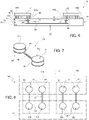
- Figure 7 shows a possible embodiment of the galvanic-coupling structures 73.
- a first and a second disk-shaped plate 92, 93 form the bottom portions 65 of Figure 5 or the top plate regions 88 of Figure 6 of the first capacitor 70 and second capacitor 71, respectively.
- a third and a fourth disk-shaped plate 94, 95 form the ends of the buried conductive region 56 of the first and second capacitors 70, 71.
- the third and fourth disk-shaped plates 94, 95 are here vertically aligned to the first disk-shaped plate 92 and the second disk-shaped plate 93, respectively.
- a conductive line 96 forms the buried conductive region 56 and directly connects the third and fourth disk-shaped plates 94, 95 together.
- the size and shape of the disk-shaped plates 92-95 and of the conductive line 96 may be decided by the designer on the basis of the desired isolation voltages and of the materials used to prevent electrical field accumulation areas (tip effect) and in general to minimize the maximum electrical field at the specific operating voltage.
- the geometrical characteristics are studied to provide desired values for the active capacitance and for the active capacitance/parasitic capacitance ratio and to minimize peeling or failure risks during thermal cycles to which the device may be subjected during manufacture or normal use.
- the system 50 may be configured to allow one of the devices 53, 54 or both (but not simultaneously) to operate at a high voltage (e.g., 10 kV or higher).
- the disk-shaped plates 92-95 may have a diameter comprised between 100 ⁇ m and 1 mm, in particular 400 ⁇ m
- the conductive line 96 may have a length comprised between 500 ⁇ m and 3 mm, in particular 1 mm, and a width comprised between 5 and 100 ⁇ m, in particular 30 ⁇ m.
- the system 50 may comprise a number of galvanic-coupling structures 73, according to the needs.
- Figure 8 shows a system 100 comprising four galvanic-coupling structures 73 forming two transmission channels 101, 102, each having a respective pair of capacitances for differential transmission of the signals.
- the signals are, for example, transmitted by the first die 51 as potential difference between two first disk-shaped plates 92 and received by the second die 52 as potential difference between two second disk-shaped plates 93, in case of transmission from the first die 51 to the second die 52, and vice versa in the transmission of signals from the second die 52 to the first die 51.
- Figure 9 shows a system 150 similar to the system 50 of Figure 5 . Consequently, the system 150 will be described only with reference to the differences, using the same reference numbers for same parts.
- the system 150 of Figure 9 again comprises two dice 51, 52 fixed to a support 55 housing a buried conductive region 56, but the latter overlies in part the external connection regions 60, 61, so that the capacitors 70, 71 are arranged vertically aligned above the external connection regions 60, 61.
- the distance between the external connection regions 60, 61 may be 500 pm, but the thickness of the support 55 must be chosen with a sufficient value, higher than for the system 50 of Figure 5 .
- the support 55 is arranged on the dice 51, 52.
- the dice 51, 52 are fixed directly to a respective external connection region 60, 61, a first contact structure 257A extends between the first die 51 and the support 55, and a second contact structure 257B extends between the first die 51 and the support 55.
- the dice 51, 52 are fixed to the respective external connection regions 60, 61, on a first main surface thereof and to the support 55, on a second main surface thereof, opposite to the first main surface.
- the contact structures 257A, 257B may be formed in a similar way to the contact structures 57A-57D described above, and thus here comprise each a bottom portion 267, for example formed by a die pad, metal region; an intermediate portion 266, forming a bump region, here arranged on the bottom portion 267; and a top portion 265, for example formed by a support pad region, of metal, here arranged on the intermediate portion 266.
- the top portions 265 of the contact structures 257A, 257B face respective ends, of the buried conductive region 56; the ends may be disk-shaped (as shown in Figure 7 ) .
- the top portions 265 of the contact structures 257A, 257B form plate regions, capacitively coupled to the buried conductive region 56, to form the capacitors 70, 71.
- the contact structures 257A, 257B may be connected by vias to respective conductive regions (not shown) formed in the support 55 and facing the ends of the buried conductive region 56.
- the length of the buried conductive region 56 may be comprised between 0.5 and 3 mm in the case of a distance between the external connection regions 60, 61 of 0.5 mm.
- the system 200 of Figure 10 has the advantage that, to obtain the desired isolation, is sufficient to satisfy the sealing constraint for the distance T1 between the second contact structure 57B and the buried conductive region 56 (and/or the third contact structure 57C and the buried conductive region 56), since the insulation condition on the distance T2 (i.e., the distance between buried conductive region 56 and the external connection regions 60, 61) is automatically satisfied.
- a substrate 58 of semiconductor material extends on the support 55 of the system 200 of Figure 10 and forms a die 59 with the support 55.
- the support 55 may be formed by insulating layers of polyimide and/or oxide housing metals to form the buried conductive region 56 and the top portions 265 of the contact structures 257A, 257B.
- the system 200 may be obtained using techniques of the semiconductor industry, with consequent advantages in terms of resolution, spatial dimensions control and alignment.
- Figure 12 shows a system 250 similar to the system 50 of Figure 5 .
- the external connection regions 60, 61 are missing, and a bottom metal layer 86 of the support 55 extends underneath the bottom insulating layer 80.
- the bottom metal layer 86 is here shaped so as to form leads (of which two leads 260, 261 are shown, similar to the external connection regions 60, 61) for external connection of the devices 53, 54.
- the system 250 of Figure 12 may have a finishing of the BGA (Ball Grid Array) type with the balls of solder paste 262 (shown dashed) remolten on the leads 260, 261.
- BGA Ball Grid Array
- the systems 50, 100, 150, 200 and 250 described herein have a high isolation level between the devices even operating at very different, high voltages. These systems moreover give rise to parasitic elements of very low value.
- the shown systems comprise only two devices, the same solution may be applied in the case of a plurality of devices, possibly with adequate spacing of the buried conductive regions 56.
Landscapes
- Semiconductor Integrated Circuits (AREA)
- Physics & Mathematics (AREA)
- Geometry (AREA)
- Superconductors And Manufacturing Methods Therefor (AREA)
Abstract
Description
- The present invention relates to a packaged electronic system formed by electrically connected and galvanically isolated dice.
- In particular, the invention relates to an electronic system where the dice are packaged in a same package and integrate electronic devices (components and/or circuits) configured to work at very different voltages and to exchange signals with each other. For instance, the electronic system may be a power-supply system, a digital isolator, a power transistor driving system, a DC-DC converter, or other system where at least one of the devices operates at high voltage (even higher than 10 kV) and/or high power. For these systems, it is known to include measures for maintaining an adequate isolation galvanic between the various devices.
- In particular, packages dedicated to providing a high isolation level are mainly based upon two approaches:
- two-dice approach, where two dice integrate each a respective "functional" device and a respective (capacitive or inductive) isolation element and the two isolation elements are connected together; and
- three-dice approach, comprising an isolation device integrated in an own die connected to the two "functional" devices.
- The two-dice approach is shown, for example, in
Figures 1 and 2 . Here apackage 5 of resin or other insulating material encloses a system comprising twodice electronic circuit 10 and arespective isolation element 11. For instance, thecircuits 10 may be ASICs (Application-Specific Integrated Circuits); alternatively, one or bothcircuits 10 may integrate individual electronic components and/or be formed by different circuits. - The
circuits 10 are connected to therespective isolation elements 11 through buried or surface connections, not shown; theisolation elements 11 in thedice connection wires 12. - The
dice element 15 that is part of a leadframe for connecting different terminals of thecircuits 10 to the outside, in a per se known manner.Bonding wires 16 connect the terminals of thecircuits 10 to therespective leadframe 15, and thepackage 5 embeds thedice wires leadframe 15 so as to electrically isolate them and protect them from the external environment. - The two-dice approach is intrinsically robust as regards parasitic elements, since the
connection wires 12 are just a few, are short, and are arranged in a less critical position (downstream of the isolation elements 11), but, in some applications, may be far from flexible. In fact, the designer has only a few degrees of freedom in the design of the isolation elements, being constrained to the technologies and platforms for manufacturing thecircuits 10. In particular, with this approach, the designer is not always able to use the most advanced approaches and knowledge and frequently cannot use the same isolation elements when thecircuits 10 of thedice - The three-dice approach is shown, for example, in
Figures 3 and 4 . Here apackage 25 of resin or other insulating material encloses a system formed by two "operative" dice (first and seconddie 28, 29). Thedice component respective leadframe third die 32 fixed on one of the two leadframes, here on theleadframe 22 carrying thefirst die 28. - The
first circuit 26 is connected to theisolation element 31 throughfirst connection wires 35, and thesecond circuit 27 is connected to theisolation element 31 throughsecond connection wires 36, generally longer than thefirst connection wires 35. -
Bonding wires 38 connect the terminals of thecircuits respective leadframes package 25 embeds thedice wires leadframes - The three-dice approach is very flexible and enables use of isolation optimized platforms, irrespective of the technology used for the
circuits first connection wires 35 and, in particular, thesecond connection wires 36, which can cause problems of cross-talk, i.e., interference between the signal-transmission channels. - Other possibilities for mutually insulating the devices arranged in a single package include arranging high-value capacitances within one or both devices. However, not even these approaches are altogether satisfactory and/or can be applied to all systems. In fact, the provision of shielding coatings cannot be used for wires of small dimensions and is subject to problems of repeatability, so that it is far from effective. The use of high capacitances is not moreover always possible since they cause an increase in power consumption of the system and can reduce the bandwidth usable for the communications.
-
US 2013/0168854 discloses a semiconductor package having a bridge interposer accommodating routing traces connected to signal pads formed by a surface of the bridge interposer. -
US 2020/0321275 discloses similar interconnects for electronic circuits. -
WO 97/24740 - Aim of the present invention is to provide a solution that overcomes the drawbacks of the prior art.
- According to the present invention a packaged electronic system is provided, as defined in the attached claims.
- For a better understanding of the present invention, some embodiments thereof are now described, purely by way of nonlimiting example, with reference to the attached drawings, wherein:
-
Figure 1 is a top view, simplified and with the package shown in phantom, of a known system of devices; -
Figure 2 is a side view of the system ofFigure 1 , with the package shown in phantom; -
Figure 3 is a top view, simplified and with the package shown in phantom, of another known system of devices; -
Figure 4 is a side view of the system ofFigure 3 , with the package shown in phantom; -
Figure 5 is a side view of an embodiment of the present system of devices, with the package shown in phantom; -
Figure 5A shows an enlarged detail ofFigure 5 ; -
Figure 6 is a side view of an implementation of a portion of the present system of devices, at an enlarged scale; -
Figure 7 is a perspective view of an implementation of a part of the present system of devices, at an enlarged scale; -
Figure 8 shows the layout of an implementation of a part of the present system of devices; -
Figure 9 is a side view of another embodiment of the present system of devices, with the package shown in phantom; -
Figure 10 is a side view of a different embodiment of the present system of devices, with the package shown in phantom; -
Figure 11 is a side view of yet another embodiment of the present system of devices, with the package shown in phantom; and -
Figure 12 is a side view of a different embodiment of the present system of devices, with the package shown in phantom. - In particular, in the following description, reference will be made to a system formed by two dice, integrating each an ASIC (Application-Specific Integrated Circuit), but the invention applies to electronic devices of any type, whether single components or more complex circuits, operating at different voltages, even having a very different value, in common mode.
-
Figure 5 shows asystem 50 comprising twodice own device devices - The
dice support 55. Thesupport 55 has, for example, a parallelepipedal shape having a first and a secondmain face Figure 5A ). The twomain faces - The
support 55 is an organic support, generally of insulating material, housing inside it a buriedconductive region 56. The buriedconductive region 56 is completely surrounded by the insulating material of thesupport 55 so that there are no physical conductive connection paths with other parts of the system 50 (in other words, the buriedconductive region 56 is floating). - For instance, the
support 55 may be formed by a printed-circuit board. According to one embodiment, thesupport 55 is formed by a multilayer including a sequence of conductive layers, typically of metal, and by insulating layers, for example of organic plastic, and one of the conductive layers forms the buriedconductive region 56, as described more fully hereinafter with reference toFigure 6 . - The buried
conductive region 56 is planar, and extends as far as underneath thedice - In the embodiment shown, the buried
conductive region 56 extends for most of the length of the support 55 (parallel to the first axis X). -
Contact structures 57A-57D extend on thefirst face 55A ofsupport 55 for electrical connection ofdice - The
contact structures 57A-57D are here formed by abottom portion 65, for example formed by a support pad region, arranged on thefirst face 55A of thesupport 55; anintermediate portion 66, forming a bump region, here arranged on thebottom portion 65; and atop portion 67, for example formed by a die pad region, here arranged on theintermediate portion 66 and formed, from example, by respective top metal layers of thedice - The
top portions 67 of thecontact structures 57A-57D are electrically connected to the electrical components of thedevices - Two contact structures, referred to hereinafter as first and
second contact structures first die 51 to thesupport 55, and two other contact structures, designated hereinafter as third andfourth contact structures second die 52 to thesupport 55. - In particular, here, the
bottom portions 65 of the second andthird contact structures conductive region 56 and are thus capacitively coupled thereto. Consequently, in this embodiment, thebottom portions 65 of the second andthird contact structures conductive region 56. In this embodiment, then, thebottom portions 65 are also referred to asfirst plates 65, and the buriedconductive region 56 is also referred to as common floatingplate 56. - In other words, the buried
conductive region 56 is a planar structure comprising portions arranged below, and capacitively coupled with, thefirst plates 65. - Thus, a
first capacitor 70 is formed between thesecond contact structure 57B and the buriedconductive region 56, and asecond capacitor 71 is formed between thethird contact structure 57C and the buriedconductive region 56. The first andsecond capacitors conductive region 56, thereby providing a galvanic-coupling structure 73 between the first andsecond dice - The first and
fourth contact structures respective dice support 55, in a way not shown and known to the person skilled in the art. - In
Figure 5 , a first and a secondexternal connection region main face 55B of thesupport 55. - The
external connection regions system 50 to the outside. In particular, the shownexternal connection regions devices external connection regions support 55 so as not to vertically overlap the buriedconductive region 56. - In
Figure 5 , afurther pad region 75 extends on thefirst face 55A of thesupport 55. Thefurther pad region 75 may be provided in the same layer as thefirst plates 65, in a way known to the person skilled in the art, and is connected to the secondexternal connection region 61 by anelectrical connection wire 76. - A
packaging mass 77, of resin or other insulating material, encloses thedice support 55, theelectrical connection wire 76, and a most of theexternal connection regions - In practice, in the
system 50 ofFigure 5 , thecapacitors devices devices - This channel can be used as single transmission channel, according to the
devices system 50 may include a plurality of such channels, each for a respective signal to be exchanged and/or a transmission direction, as discussed in detail hereinafter. - In the
system 50 ofFigure 5 , to obtain the desired isolation, and according to the specific operating voltages, some distance ratios are important, as discussed hereinafter, on the exemplary hypothesis that thefirst die 51 operates at a much higher voltage than the firstexternal connection region 60. - In particular, with reference to
Figures 5 and 5A , the distance D2 between theexternal connection regions dice - Furthermore, the distance T1 (
Figure 5A ) between thesecond contact structure 57B and the buriedconductive region 56 and the distance T2 between the buriedconductive region 56 and the firstexternal connection region 60 are chosen, to take into account the isolation characteristics of the material of thesupport 55 and other possible criteria known to the designer. For instance, if the material of the insulating layers forming thesupport 55 is the same, with the same dielectric strength, the distances T1 and T2 may be equal (T1 = T2). Vice versa, if the bottom portion (inFigure 5A ) of thesupport 55 is of a material able to withstand higher electrical fields than the material interposed between the buriedconductive region 56 and the first plate 65 (bottom portion of thesecond contact structure 57B), T1 may be higher than T2 (T1 > T2). In general, T1 ≥ T2. - Similar considerations may be applied to the distance between the
third contact structures 57C and the buriedconductive region 56 and to the distance between the buriedconductive region 56 and the secondexternal connection region 61, in case of large voltage differences. -
Figure 6 shows a possible implementation of thesupport 55. - In detail, the
support 55 ofFigure 6 is manufactured starting from a board of a commercially available type, formed by a multilayer. In particular, here thesupport 55 comprises a bottom insulatinglayer 80; a bottomconductive layer 81, overlying the bottom insulatinglayer 80; an intermediate insulatinglayer 82, the so called core, overlying the bottom insulatinglayer 80 and the bottomconductive layer 81; a topconductive layer 83, overlying the intermediate insulatinglayer 82; a top insulatinglayer 84, overlying the intermediate insulatinglayer 82 and the topconductive layer 83; and a topconductive layer 85, overlying the top insulatinglayer 84. - The insulating layers 80, 82, 84 may be of organic material, for example plastic, such as so-called insulating prepeg; the
conductive layers conductive layer 83 may further comprise a layer with very low contact resistance, for example a gold-based layer, overlying the copper layer. - The
conductive layers conductive region 56, thetop plate regions 88 of thecapacitors bottom portions 65 of the second andthird contact structures - In a way not shown, the
support 55 may comprise a bottom conductive layer, arranged underneath the bottom insulatinglayer 80 and also of metal, such as copper, possibly coated with a gold-based layer (see also the description ofFigure 12 ) . - In practice, here the
capacitors layer 82, and the top conductive layer 83 (top plate regions 88). Consequently, in this embodiment, thebottom portions 65 of thecontact structures 57A-57D no longer form plates of thecapacitors top plate regions 88 byrespective vias 90 extending through the top insulatinglayer 84. - In this embodiment, the critical distance T1, to be compared with the distance T2 between the buried
conductive region 56 and the first external connection region 60 (not shown inFigure 6 ), is the one between thebottom portion 65 of thesecond contact structures 57B and thetop plate region 88 facing it. -
Figure 7 shows a possible embodiment of the galvanic-coupling structures 73. - In detail, here, a first and a second disk-shaped
plate bottom portions 65 ofFigure 5 or thetop plate regions 88 ofFigure 6 of thefirst capacitor 70 andsecond capacitor 71, respectively. A third and a fourth disk-shapedplate conductive region 56 of the first andsecond capacitors - The third and fourth disk-shaped
plates plate 92 and the second disk-shapedplate 93, respectively. - A
conductive line 96 forms the buriedconductive region 56 and directly connects the third and fourth disk-shapedplates - The size and shape of the disk-shaped plates 92-95 and of the
conductive line 96 may be decided by the designer on the basis of the desired isolation voltages and of the materials used to prevent electrical field accumulation areas (tip effect) and in general to minimize the maximum electrical field at the specific operating voltage. In particular, in a way known to the person skilled in the art, the geometrical characteristics are studied to provide desired values for the active capacitance and for the active capacitance/parasitic capacitance ratio and to minimize peeling or failure risks during thermal cycles to which the device may be subjected during manufacture or normal use. - For instance, the
system 50 may be configured to allow one of thedevices conductive line 96 may have a length comprised between 500 µm and 3 mm, in particular 1 mm, and a width comprised between 5 and 100 µm, in particular 30 µm. - The
system 50 may comprise a number of galvanic-coupling structures 73, according to the needs. - For instance,
Figure 8 shows asystem 100 comprising four galvanic-coupling structures 73 forming twotransmission channels first die 51 as potential difference between two first disk-shapedplates 92 and received by thesecond die 52 as potential difference between two second disk-shapedplates 93, in case of transmission from thefirst die 51 to thesecond die 52, and vice versa in the transmission of signals from thesecond die 52 to thefirst die 51. -
Figure 9 shows asystem 150 similar to thesystem 50 ofFigure 5 . Consequently, thesystem 150 will be described only with reference to the differences, using the same reference numbers for same parts. - The
system 150 ofFigure 9 again comprises twodice support 55 housing a buriedconductive region 56, but the latter overlies in part theexternal connection regions capacitors external connection regions external connection regions support 55 must be chosen with a sufficient value, higher than for thesystem 50 ofFigure 5 . - In the
system 200 ofFigure 10 , thesupport 55 is arranged on thedice - In detail, here the
dice external connection region first contact structure 257A extends between thefirst die 51 and thesupport 55, and asecond contact structure 257B extends between thefirst die 51 and thesupport 55. In practice, thedice external connection regions support 55, on a second main surface thereof, opposite to the first main surface. - The
contact structures contact structures 57A-57D described above, and thus here comprise each abottom portion 267, for example formed by a die pad, metal region; anintermediate portion 266, forming a bump region, here arranged on thebottom portion 267; and atop portion 265, for example formed by a support pad region, of metal, here arranged on theintermediate portion 266. - The
top portions 265 of thecontact structures conductive region 56; the ends may be disk-shaped (as shown inFigure 7 ) . Here, then, thetop portions 265 of thecontact structures conductive region 56, to form thecapacitors - Alternatively, in a way similar to what shown in
Figure 6 for thesystem 50, thecontact structures support 55 and facing the ends of the buriedconductive region 56. - In the
system 200 ofFigure 10 , the length of the buriedconductive region 56 may be comprised between 0.5 and 3 mm in the case of a distance between theexternal connection regions - The
system 200 ofFigure 10 has the advantage that, to obtain the desired isolation, is sufficient to satisfy the sealing constraint for the distance T1 between thesecond contact structure 57B and the buried conductive region 56 (and/or thethird contact structure 57C and the buried conductive region 56), since the insulation condition on the distance T2 (i.e., the distance between buriedconductive region 56 and theexternal connection regions 60, 61) is automatically satisfied. - According to a different embodiment, shown in
Figure 11 , asubstrate 58 of semiconductor material extends on thesupport 55 of thesystem 200 ofFigure 10 and forms a die 59 with thesupport 55. In this case, thesupport 55 may be formed by insulating layers of polyimide and/or oxide housing metals to form the buriedconductive region 56 and thetop portions 265 of thecontact structures - In this way, the
system 200 may be obtained using techniques of the semiconductor industry, with consequent advantages in terms of resolution, spatial dimensions control and alignment. -
Figure 12 shows asystem 250 similar to thesystem 50 ofFigure 5 . - In the
system 250, theexternal connection regions bottom metal layer 86 of thesupport 55 extends underneath the bottom insulatinglayer 80. Thebottom metal layer 86 is here shaped so as to form leads (of which two leads 260, 261 are shown, similar to theexternal connection regions 60, 61) for external connection of thedevices - The
system 250 ofFigure 12 may have a finishing of the BGA (Ball Grid Array) type with the balls of solder paste 262 (shown dashed) remolten on theleads - The
systems - They may be manufactured in a simple way, using machines and steps ordinary in the production of power devices.
- Finally, it is clear that modifications and variations may be made to the system described and shown herein, without departing from the scope of the present invention, as defined in the attached claims. For instance, the different described embodiments may be combined so as to provide further solutions.
- Moreover, even though the shown systems comprise only two devices, the same solution may be applied in the case of a plurality of devices, possibly with adequate spacing of the buried
conductive regions 56.
Claims (12)
- A packaged electronic system comprising:a support (55), the support comprising an insulating organic substrate housing a buried conductive region (56), the buried conductive region being a floating region and having a first and a second portion (94; 95) mutually spaced;a first die (51), fixed to the support, the first die having a first main surface carrying a first die contact region (67; 267) capacitively coupled to the first portion of the buried conductive region;a second die (52), fixed to the support, the second die having a first main surface carrying a second die contact region (67; 267), capacitively coupled to the second portion of the buried conductive region; anda packaging mass (77) enclosing the first die (51), the second die (52), the first die contact region, the second die contact region, and, at least partially, the support (55),wherein the buried conductive region (56) is planar.
- The system according to claim 1, comprising a first and a second contact structure (57B, 57C) arranged on the first face (55A) of the support (55), wherein:the first contact structure (57B, 57C) comprises a first plate region (65), capacitively coupled to the first portion (94) of the buried conductive region (56); andthe second contact structure comprises a second plate region (65), capacitively coupled to the second portion (95) of the buried conductive region (56).
- The system according to claim 1 or 2, wherein the buried conductive region (56) has an elongated shape with a first end and a second end, wherein the first portion (94) of the buried conductive region is arranged at the first end and the second portion (95) of the buried conductive region is arranged at the second end of the buried conductive region.
- The system according to the preceding claim, wherein the first and second ends (94; 95) of the buried conductive region (56) are disk-shaped.
- The system according to any of the preceding claims, wherein the first and second die contact regions (67; 267) face the first and, respectively, the second portions (94; 95), of the buried conductive region (56).
- The system according to the preceding claim, comprising a first and a second external connection region (60, 61) of metallic material, the first and second external connection regions extending on a second face (55B) of the support (55) at a first mutual distance (D2), the external connection regions being electrically connected by connection lines (76) to the first and second dice (51, 52).
- The system according to the preceding claim, wherein the first and second dice (51, 52) are arranged at a second mutual distance (D1), wherein the first distance (D2) is greater than the second distance.
- The system according to claim 6, wherein the first and second dice (51, 52) are arranged at a second mutual distance (D1), wherein the first distance (D2) is smaller than the second distance.
- The system according to any of claims 6-8, wherein the distance (T2) between the buried conductive region (56) and the first external connection region (60) is lower or equal to the distance (T1) between the buried conductive region (56) and the first contact structure (57B, 57C).
- The system according to any of claims 2-9, wherein:the first contact structure (57B, 57C) further comprises a first bump region (66), contiguous to the first plate region and to the first die contact region, andthe second contact structure further comprises a second bump region (66), contiguous to the second plate region and to the second die contact region.
- The system according to any of claims 1-5, wherein the first and second dice (51, 52) have a respective second main surface, the first and second dice (51, 52) being fixed to the support (55) on the respective first main surface and to a respective external connection region (60, 61), of metal, on the respective second main surface.
- The system according to any of claims 2-11, wherein:the support (55) is a multilayer formed by a plurality of conductive layers including at least a first, a second and a third conductive layer (81, 83, 85) spaced apart by respective insulating layers (82, 84),the buried conductive region (56) is formed in the first conductive layer (81) of the plurality of conductive layers,a first and a second capacitive plate region (88) are formed in the second conductive layer (83) and directly face the first and, respectively, the second portions (94, 95) of the buried conductive region (56), andthe first and second support contact regions (65; 265) are formed in the third conductive layer (85) and are electrically connected to the first and, respectively, the second capacitive plate regions (88), through vias (90) extending across a respective insulating layer (84).
Applications Claiming Priority (1)
| Application Number | Priority Date | Filing Date | Title |
|---|---|---|---|
| IT102021000001637A IT202100001637A1 (en) | 2021-01-27 | 2021-01-27 | ENCAPSULATED ELECTRONIC SYSTEM FORMED BY PLATES ELECTRICALLY COUPLED AND GALVANICALLY INSULATED |
Publications (2)
| Publication Number | Publication Date |
|---|---|
| EP4036968A1 true EP4036968A1 (en) | 2022-08-03 |
| EP4036968B1 EP4036968B1 (en) | 2024-05-01 |
Family
ID=75340159
Family Applications (1)
| Application Number | Title | Priority Date | Filing Date |
|---|---|---|---|
| EP22153019.9A Active EP4036968B1 (en) | 2021-01-27 | 2022-01-24 | Packaged electronic system formed by electrically connected and galvanically isolated dice |
Country Status (4)
| Country | Link |
|---|---|
| US (1) | US12354998B2 (en) |
| EP (1) | EP4036968B1 (en) |
| CN (2) | CN217544608U (en) |
| IT (1) | IT202100001637A1 (en) |
Cited By (1)
| Publication number | Priority date | Publication date | Assignee | Title |
|---|---|---|---|---|
| WO2025223865A1 (en) * | 2024-04-24 | 2025-10-30 | Robert Bosch Gmbh | Multi-chip module and method for producing a multi-chip module |
Families Citing this family (3)
| Publication number | Priority date | Publication date | Assignee | Title |
|---|---|---|---|---|
| IT202100001637A1 (en) * | 2021-01-27 | 2022-07-27 | St Microelectronics Srl | ENCAPSULATED ELECTRONIC SYSTEM FORMED BY PLATES ELECTRICALLY COUPLED AND GALVANICALLY INSULATED |
| EP4668334A1 (en) * | 2024-06-18 | 2025-12-24 | Nexperia B.V. | A leadless package comprising a first and a second semiconductor die, wherein a galvanic coupling is provided between those semiconductor dies, as well as a corresponding method |
| EP4668335A1 (en) * | 2024-06-18 | 2025-12-24 | Nexperia B.V. | A package comprising a first and a second semiconductor die, wherein a galvanic coupling is provided between those semiconductor dies, as well as a corresponding method |
Citations (5)
| Publication number | Priority date | Publication date | Assignee | Title |
|---|---|---|---|---|
| WO1997024740A1 (en) | 1995-12-18 | 1997-07-10 | Douglass Barry G | High density inter-chip connections by electromagnetic coupling |
| US20090168391A1 (en) * | 2007-12-27 | 2009-07-02 | Kouichi Saitou | Substrate for mounting device and method for producing the same, semiconductor module and method for producing the same, and portable apparatus provided with the same |
| US20110298139A1 (en) * | 2010-06-04 | 2011-12-08 | Yi-Shao Lai | Semiconductor Package |
| US20130168854A1 (en) | 2011-12-28 | 2013-07-04 | Broadcom Corporation | Semiconductor Package with a Bridge Interposer |
| US20200321275A1 (en) | 2019-04-02 | 2020-10-08 | Invensas Corporation | Over and under interconnects |
Family Cites Families (9)
| Publication number | Priority date | Publication date | Assignee | Title |
|---|---|---|---|---|
| TWM266543U (en) * | 2004-10-28 | 2005-06-01 | Advanced Semiconductor Eng | Multi-chip stack package |
| US9642259B2 (en) * | 2013-10-30 | 2017-05-02 | Qualcomm Incorporated | Embedded bridge structure in a substrate |
| US9735112B2 (en) * | 2014-01-10 | 2017-08-15 | Fairchild Semiconductor Corporation | Isolation between semiconductor components |
| US11488906B2 (en) * | 2019-01-24 | 2022-11-01 | Samsung Electro-Mechanics Co., Ltd. | Bridge embedded interposer, and package substrate and semiconductor package comprising the same |
| US11380653B2 (en) * | 2019-08-27 | 2022-07-05 | Taiwan Semiconductor Manufacturing Company, Ltd. | Die stack structure and manufacturing method thereof |
| US11264359B2 (en) * | 2020-04-27 | 2022-03-01 | Taiwan Semiconductor Manufacturing Co., Ltd. | Chip bonded to a redistribution structure with curved conductive lines |
| US11626337B2 (en) * | 2020-05-19 | 2023-04-11 | Amkor Technology Singapore Holding Pte. Ltd. | Semiconductor devices and methods of manufacturing semiconductor devices |
| US11605571B2 (en) * | 2020-05-29 | 2023-03-14 | Qualcomm Incorporated | Package comprising a substrate, an integrated device, and an encapsulation layer with undercut |
| IT202100001637A1 (en) * | 2021-01-27 | 2022-07-27 | St Microelectronics Srl | ENCAPSULATED ELECTRONIC SYSTEM FORMED BY PLATES ELECTRICALLY COUPLED AND GALVANICALLY INSULATED |
-
2021
- 2021-01-27 IT IT102021000001637A patent/IT202100001637A1/en unknown
-
2022
- 2022-01-20 US US17/580,480 patent/US12354998B2/en active Active
- 2022-01-24 EP EP22153019.9A patent/EP4036968B1/en active Active
- 2022-01-26 CN CN202220214158.9U patent/CN217544608U/en active Active
- 2022-01-26 CN CN202210092662.0A patent/CN114823637B/en active Active
Patent Citations (5)
| Publication number | Priority date | Publication date | Assignee | Title |
|---|---|---|---|---|
| WO1997024740A1 (en) | 1995-12-18 | 1997-07-10 | Douglass Barry G | High density inter-chip connections by electromagnetic coupling |
| US20090168391A1 (en) * | 2007-12-27 | 2009-07-02 | Kouichi Saitou | Substrate for mounting device and method for producing the same, semiconductor module and method for producing the same, and portable apparatus provided with the same |
| US20110298139A1 (en) * | 2010-06-04 | 2011-12-08 | Yi-Shao Lai | Semiconductor Package |
| US20130168854A1 (en) | 2011-12-28 | 2013-07-04 | Broadcom Corporation | Semiconductor Package with a Bridge Interposer |
| US20200321275A1 (en) | 2019-04-02 | 2020-10-08 | Invensas Corporation | Over and under interconnects |
Cited By (1)
| Publication number | Priority date | Publication date | Assignee | Title |
|---|---|---|---|---|
| WO2025223865A1 (en) * | 2024-04-24 | 2025-10-30 | Robert Bosch Gmbh | Multi-chip module and method for producing a multi-chip module |
Also Published As
| Publication number | Publication date |
|---|---|
| EP4036968B1 (en) | 2024-05-01 |
| US12354998B2 (en) | 2025-07-08 |
| US20220238485A1 (en) | 2022-07-28 |
| CN114823637B (en) | 2026-02-06 |
| IT202100001637A1 (en) | 2022-07-27 |
| CN217544608U (en) | 2022-10-04 |
| CN114823637A (en) | 2022-07-29 |
Similar Documents
| Publication | Publication Date | Title |
|---|---|---|
| EP4036968B1 (en) | Packaged electronic system formed by electrically connected and galvanically isolated dice | |
| US7129571B2 (en) | Semiconductor chip package having decoupling capacitor and manufacturing method thereof | |
| US8885356B2 (en) | Enhanced stacked microelectronic assemblies with central contacts and improved ground or power distribution | |
| KR101564070B1 (en) | Printed circuit board and semiconductor package using the same | |
| US6995043B2 (en) | Methods for fabricating routing elements for multichip modules | |
| US7078794B2 (en) | Chip package and process for forming the same | |
| KR20080057190A (en) | 3D electronic packaging structure with improved grounding performance and embedded antenna | |
| US8791501B1 (en) | Integrated passive device structure and method | |
| US12327821B2 (en) | Semiconductor package having chip stack | |
| US11183483B2 (en) | Multichip module and electronic device | |
| KR100876881B1 (en) | Pad part of semiconductor device | |
| TWI493668B (en) | Pad structure, line carrier board and integrated circuit chip | |
| US6605876B2 (en) | Semiconductor chip package and connection structure including a ground metal plane having blank patterns | |
| KR20160101502A (en) | Rf package and manufacturing method thereof | |
| KR101489678B1 (en) | Intermediate for electronic component mounting structure, electronic component mounting structure, and method for manufacturing electronic component mounting structure | |
| US20260144148A1 (en) | Semiconductor package | |
| KR19980078349A (en) | Semiconductor package and manufacturing method | |
| KR100834835B1 (en) | Semiconductor device with built-in capacitor and manufacturing method thereof | |
| WO2025100041A1 (en) | Semiconductor package and rf module | |
| CN118693029A (en) | Isolator | |
| JP2010278084A (en) | Semiconductor device | |
| CN121172026A (en) | Leadless package comprising a first semiconductor die and a second semiconductor die, and corresponding method, wherein a galvanic coupling is provided between these semiconductor dies | |
| KR20050027067A (en) | Semiconductor apparatus | |
| JP2014096504A (en) | Semiconductor device |
Legal Events
| Date | Code | Title | Description |
|---|---|---|---|
| PUAI | Public reference made under article 153(3) epc to a published international application that has entered the european phase |
Free format text: ORIGINAL CODE: 0009012 |
|
| STAA | Information on the status of an ep patent application or granted ep patent |
Free format text: STATUS: THE APPLICATION HAS BEEN PUBLISHED |
|
| AK | Designated contracting states |
Kind code of ref document: A1 Designated state(s): AL AT BE BG CH CY CZ DE DK EE ES FI FR GB GR HR HU IE IS IT LI LT LU LV MC MK MT NL NO PL PT RO RS SE SI SK SM TR |
|
| STAA | Information on the status of an ep patent application or granted ep patent |
Free format text: STATUS: REQUEST FOR EXAMINATION WAS MADE |
|
| 17P | Request for examination filed |
Effective date: 20221213 |
|
| RBV | Designated contracting states (corrected) |
Designated state(s): AL AT BE BG CH CY CZ DE DK EE ES FI FR GB GR HR HU IE IS IT LI LT LU LV MC MK MT NL NO PL PT RO RS SE SI SK SM TR |
|
| GRAP | Despatch of communication of intention to grant a patent |
Free format text: ORIGINAL CODE: EPIDOSNIGR1 |
|
| STAA | Information on the status of an ep patent application or granted ep patent |
Free format text: STATUS: GRANT OF PATENT IS INTENDED |
|
| INTG | Intention to grant announced |
Effective date: 20231121 |
|
| GRAS | Grant fee paid |
Free format text: ORIGINAL CODE: EPIDOSNIGR3 |
|
| GRAA | (expected) grant |
Free format text: ORIGINAL CODE: 0009210 |
|
| STAA | Information on the status of an ep patent application or granted ep patent |
Free format text: STATUS: THE PATENT HAS BEEN GRANTED |
|
| AK | Designated contracting states |
Kind code of ref document: B1 Designated state(s): AL AT BE BG CH CY CZ DE DK EE ES FI FR GB GR HR HU IE IS IT LI LT LU LV MC MK MT NL NO PL PT RO RS SE SI SK SM TR |
|
| REG | Reference to a national code |
Ref country code: GB Ref legal event code: FG4D |
|
| REG | Reference to a national code |
Ref country code: CH Ref legal event code: EP |
|
| REG | Reference to a national code |
Ref country code: IE Ref legal event code: FG4D |
|
| REG | Reference to a national code |
Ref country code: DE Ref legal event code: R096 Ref document number: 602022003085 Country of ref document: DE |
|
| REG | Reference to a national code |
Ref country code: LT Ref legal event code: MG9D |
|
| REG | Reference to a national code |
Ref country code: NL Ref legal event code: MP Effective date: 20240501 |
|
| PG25 | Lapsed in a contracting state [announced via postgrant information from national office to epo] |
Ref country code: IS Free format text: LAPSE BECAUSE OF FAILURE TO SUBMIT A TRANSLATION OF THE DESCRIPTION OR TO PAY THE FEE WITHIN THE PRESCRIBED TIME-LIMIT Effective date: 20240901 |
|
| PG25 | Lapsed in a contracting state [announced via postgrant information from national office to epo] |
Ref country code: BG Free format text: LAPSE BECAUSE OF FAILURE TO SUBMIT A TRANSLATION OF THE DESCRIPTION OR TO PAY THE FEE WITHIN THE PRESCRIBED TIME-LIMIT Effective date: 20240501 |
|
| PG25 | Lapsed in a contracting state [announced via postgrant information from national office to epo] |
Ref country code: HR Free format text: LAPSE BECAUSE OF FAILURE TO SUBMIT A TRANSLATION OF THE DESCRIPTION OR TO PAY THE FEE WITHIN THE PRESCRIBED TIME-LIMIT Effective date: 20240501 Ref country code: FI Free format text: LAPSE BECAUSE OF FAILURE TO SUBMIT A TRANSLATION OF THE DESCRIPTION OR TO PAY THE FEE WITHIN THE PRESCRIBED TIME-LIMIT Effective date: 20240501 |
|
| PG25 | Lapsed in a contracting state [announced via postgrant information from national office to epo] |
Ref country code: GR Free format text: LAPSE BECAUSE OF FAILURE TO SUBMIT A TRANSLATION OF THE DESCRIPTION OR TO PAY THE FEE WITHIN THE PRESCRIBED TIME-LIMIT Effective date: 20240802 |
|
| PG25 | Lapsed in a contracting state [announced via postgrant information from national office to epo] |
Ref country code: PT Free format text: LAPSE BECAUSE OF FAILURE TO SUBMIT A TRANSLATION OF THE DESCRIPTION OR TO PAY THE FEE WITHIN THE PRESCRIBED TIME-LIMIT Effective date: 20240902 |
|
| REG | Reference to a national code |
Ref country code: AT Ref legal event code: MK05 Ref document number: 1683605 Country of ref document: AT Kind code of ref document: T Effective date: 20240501 |
|
| PG25 | Lapsed in a contracting state [announced via postgrant information from national office to epo] |
Ref country code: NL Free format text: LAPSE BECAUSE OF FAILURE TO SUBMIT A TRANSLATION OF THE DESCRIPTION OR TO PAY THE FEE WITHIN THE PRESCRIBED TIME-LIMIT Effective date: 20240501 |
|
| PG25 | Lapsed in a contracting state [announced via postgrant information from national office to epo] |
Ref country code: ES Free format text: LAPSE BECAUSE OF FAILURE TO SUBMIT A TRANSLATION OF THE DESCRIPTION OR TO PAY THE FEE WITHIN THE PRESCRIBED TIME-LIMIT Effective date: 20240501 |
|
| PG25 | Lapsed in a contracting state [announced via postgrant information from national office to epo] |
Ref country code: AT Free format text: LAPSE BECAUSE OF FAILURE TO SUBMIT A TRANSLATION OF THE DESCRIPTION OR TO PAY THE FEE WITHIN THE PRESCRIBED TIME-LIMIT Effective date: 20240501 |
|
| PG25 | Lapsed in a contracting state [announced via postgrant information from national office to epo] |
Ref country code: PL Free format text: LAPSE BECAUSE OF FAILURE TO SUBMIT A TRANSLATION OF THE DESCRIPTION OR TO PAY THE FEE WITHIN THE PRESCRIBED TIME-LIMIT Effective date: 20240501 |
|
| PG25 | Lapsed in a contracting state [announced via postgrant information from national office to epo] |
Ref country code: LV Free format text: LAPSE BECAUSE OF FAILURE TO SUBMIT A TRANSLATION OF THE DESCRIPTION OR TO PAY THE FEE WITHIN THE PRESCRIBED TIME-LIMIT Effective date: 20240501 |
|
| PG25 | Lapsed in a contracting state [announced via postgrant information from national office to epo] |
Ref country code: PT Free format text: LAPSE BECAUSE OF FAILURE TO SUBMIT A TRANSLATION OF THE DESCRIPTION OR TO PAY THE FEE WITHIN THE PRESCRIBED TIME-LIMIT Effective date: 20240902 Ref country code: PL Free format text: LAPSE BECAUSE OF FAILURE TO SUBMIT A TRANSLATION OF THE DESCRIPTION OR TO PAY THE FEE WITHIN THE PRESCRIBED TIME-LIMIT Effective date: 20240501 Ref country code: NO Free format text: LAPSE BECAUSE OF FAILURE TO SUBMIT A TRANSLATION OF THE DESCRIPTION OR TO PAY THE FEE WITHIN THE PRESCRIBED TIME-LIMIT Effective date: 20240801 Ref country code: NL Free format text: LAPSE BECAUSE OF FAILURE TO SUBMIT A TRANSLATION OF THE DESCRIPTION OR TO PAY THE FEE WITHIN THE PRESCRIBED TIME-LIMIT Effective date: 20240501 Ref country code: LV Free format text: LAPSE BECAUSE OF FAILURE TO SUBMIT A TRANSLATION OF THE DESCRIPTION OR TO PAY THE FEE WITHIN THE PRESCRIBED TIME-LIMIT Effective date: 20240501 Ref country code: IS Free format text: LAPSE BECAUSE OF FAILURE TO SUBMIT A TRANSLATION OF THE DESCRIPTION OR TO PAY THE FEE WITHIN THE PRESCRIBED TIME-LIMIT Effective date: 20240901 Ref country code: HR Free format text: LAPSE BECAUSE OF FAILURE TO SUBMIT A TRANSLATION OF THE DESCRIPTION OR TO PAY THE FEE WITHIN THE PRESCRIBED TIME-LIMIT Effective date: 20240501 Ref country code: GR Free format text: LAPSE BECAUSE OF FAILURE TO SUBMIT A TRANSLATION OF THE DESCRIPTION OR TO PAY THE FEE WITHIN THE PRESCRIBED TIME-LIMIT Effective date: 20240802 Ref country code: FI Free format text: LAPSE BECAUSE OF FAILURE TO SUBMIT A TRANSLATION OF THE DESCRIPTION OR TO PAY THE FEE WITHIN THE PRESCRIBED TIME-LIMIT Effective date: 20240501 Ref country code: ES Free format text: LAPSE BECAUSE OF FAILURE TO SUBMIT A TRANSLATION OF THE DESCRIPTION OR TO PAY THE FEE WITHIN THE PRESCRIBED TIME-LIMIT Effective date: 20240501 Ref country code: BG Free format text: LAPSE BECAUSE OF FAILURE TO SUBMIT A TRANSLATION OF THE DESCRIPTION OR TO PAY THE FEE WITHIN THE PRESCRIBED TIME-LIMIT Effective date: 20240501 Ref country code: AT Free format text: LAPSE BECAUSE OF FAILURE TO SUBMIT A TRANSLATION OF THE DESCRIPTION OR TO PAY THE FEE WITHIN THE PRESCRIBED TIME-LIMIT Effective date: 20240501 Ref country code: RS Free format text: LAPSE BECAUSE OF FAILURE TO SUBMIT A TRANSLATION OF THE DESCRIPTION OR TO PAY THE FEE WITHIN THE PRESCRIBED TIME-LIMIT Effective date: 20240801 |
|
| PG25 | Lapsed in a contracting state [announced via postgrant information from national office to epo] |
Ref country code: DK Free format text: LAPSE BECAUSE OF FAILURE TO SUBMIT A TRANSLATION OF THE DESCRIPTION OR TO PAY THE FEE WITHIN THE PRESCRIBED TIME-LIMIT Effective date: 20240501 |
|
| PG25 | Lapsed in a contracting state [announced via postgrant information from national office to epo] |
Ref country code: EE Free format text: LAPSE BECAUSE OF FAILURE TO SUBMIT A TRANSLATION OF THE DESCRIPTION OR TO PAY THE FEE WITHIN THE PRESCRIBED TIME-LIMIT Effective date: 20240501 |
|
| PG25 | Lapsed in a contracting state [announced via postgrant information from national office to epo] |
Ref country code: CZ Free format text: LAPSE BECAUSE OF FAILURE TO SUBMIT A TRANSLATION OF THE DESCRIPTION OR TO PAY THE FEE WITHIN THE PRESCRIBED TIME-LIMIT Effective date: 20240501 |
|
| PG25 | Lapsed in a contracting state [announced via postgrant information from national office to epo] |
Ref country code: RO Free format text: LAPSE BECAUSE OF FAILURE TO SUBMIT A TRANSLATION OF THE DESCRIPTION OR TO PAY THE FEE WITHIN THE PRESCRIBED TIME-LIMIT Effective date: 20240501 Ref country code: SK Free format text: LAPSE BECAUSE OF FAILURE TO SUBMIT A TRANSLATION OF THE DESCRIPTION OR TO PAY THE FEE WITHIN THE PRESCRIBED TIME-LIMIT Effective date: 20240501 |
|
| PG25 | Lapsed in a contracting state [announced via postgrant information from national office to epo] |
Ref country code: SM Free format text: LAPSE BECAUSE OF FAILURE TO SUBMIT A TRANSLATION OF THE DESCRIPTION OR TO PAY THE FEE WITHIN THE PRESCRIBED TIME-LIMIT Effective date: 20240501 |
|
| PG25 | Lapsed in a contracting state [announced via postgrant information from national office to epo] |
Ref country code: SM Free format text: LAPSE BECAUSE OF FAILURE TO SUBMIT A TRANSLATION OF THE DESCRIPTION OR TO PAY THE FEE WITHIN THE PRESCRIBED TIME-LIMIT Effective date: 20240501 Ref country code: SK Free format text: LAPSE BECAUSE OF FAILURE TO SUBMIT A TRANSLATION OF THE DESCRIPTION OR TO PAY THE FEE WITHIN THE PRESCRIBED TIME-LIMIT Effective date: 20240501 Ref country code: RO Free format text: LAPSE BECAUSE OF FAILURE TO SUBMIT A TRANSLATION OF THE DESCRIPTION OR TO PAY THE FEE WITHIN THE PRESCRIBED TIME-LIMIT Effective date: 20240501 Ref country code: EE Free format text: LAPSE BECAUSE OF FAILURE TO SUBMIT A TRANSLATION OF THE DESCRIPTION OR TO PAY THE FEE WITHIN THE PRESCRIBED TIME-LIMIT Effective date: 20240501 Ref country code: DK Free format text: LAPSE BECAUSE OF FAILURE TO SUBMIT A TRANSLATION OF THE DESCRIPTION OR TO PAY THE FEE WITHIN THE PRESCRIBED TIME-LIMIT Effective date: 20240501 Ref country code: CZ Free format text: LAPSE BECAUSE OF FAILURE TO SUBMIT A TRANSLATION OF THE DESCRIPTION OR TO PAY THE FEE WITHIN THE PRESCRIBED TIME-LIMIT Effective date: 20240501 |
|
| REG | Reference to a national code |
Ref country code: DE Ref legal event code: R097 Ref document number: 602022003085 Country of ref document: DE |
|
| PG25 | Lapsed in a contracting state [announced via postgrant information from national office to epo] |
Ref country code: IT Free format text: LAPSE BECAUSE OF FAILURE TO SUBMIT A TRANSLATION OF THE DESCRIPTION OR TO PAY THE FEE WITHIN THE PRESCRIBED TIME-LIMIT Effective date: 20240501 |
|
| PLBE | No opposition filed within time limit |
Free format text: ORIGINAL CODE: 0009261 |
|
| STAA | Information on the status of an ep patent application or granted ep patent |
Free format text: STATUS: NO OPPOSITION FILED WITHIN TIME LIMIT |
|
| 26N | No opposition filed |
Effective date: 20250204 |
|
| PGFP | Annual fee paid to national office [announced via postgrant information from national office to epo] |
Ref country code: DE Payment date: 20241218 Year of fee payment: 4 |
|
| PG25 | Lapsed in a contracting state [announced via postgrant information from national office to epo] |
Ref country code: SI Free format text: LAPSE BECAUSE OF FAILURE TO SUBMIT A TRANSLATION OF THE DESCRIPTION OR TO PAY THE FEE WITHIN THE PRESCRIBED TIME-LIMIT Effective date: 20240501 |
|
| REG | Reference to a national code |
Ref country code: CH Ref legal event code: PL |
|
| PG25 | Lapsed in a contracting state [announced via postgrant information from national office to epo] |
Ref country code: SE Free format text: LAPSE BECAUSE OF FAILURE TO SUBMIT A TRANSLATION OF THE DESCRIPTION OR TO PAY THE FEE WITHIN THE PRESCRIBED TIME-LIMIT Effective date: 20240501 |
|
| PG25 | Lapsed in a contracting state [announced via postgrant information from national office to epo] |
Ref country code: MC Free format text: LAPSE BECAUSE OF FAILURE TO SUBMIT A TRANSLATION OF THE DESCRIPTION OR TO PAY THE FEE WITHIN THE PRESCRIBED TIME-LIMIT Effective date: 20240501 Ref country code: LU Free format text: LAPSE BECAUSE OF NON-PAYMENT OF DUE FEES Effective date: 20250124 |
|
| PG25 | Lapsed in a contracting state [announced via postgrant information from national office to epo] |
Ref country code: BE Free format text: LAPSE BECAUSE OF NON-PAYMENT OF DUE FEES Effective date: 20250131 |
|
| PG25 | Lapsed in a contracting state [announced via postgrant information from national office to epo] |
Ref country code: FR Free format text: LAPSE BECAUSE OF NON-PAYMENT OF DUE FEES Effective date: 20250131 |
|
| PG25 | Lapsed in a contracting state [announced via postgrant information from national office to epo] |
Ref country code: CH Free format text: LAPSE BECAUSE OF NON-PAYMENT OF DUE FEES Effective date: 20250131 |
|
| REG | Reference to a national code |
Ref country code: BE Ref legal event code: MM Effective date: 20250131 |
|
| REG | Reference to a national code |
Ref country code: DE Ref legal event code: R079 Ref document number: 602022003085 Country of ref document: DE Free format text: PREVIOUS MAIN CLASS: H01L0023480000 Ipc: H10W0072000000 |
|
| PG25 | Lapsed in a contracting state [announced via postgrant information from national office to epo] |
Ref country code: IE Free format text: LAPSE BECAUSE OF NON-PAYMENT OF DUE FEES Effective date: 20250124 |