EP4033556B1 - Organic electroluminescent device - Google Patents
Organic electroluminescent device Download PDFInfo
- Publication number
- EP4033556B1 EP4033556B1 EP20865694.2A EP20865694A EP4033556B1 EP 4033556 B1 EP4033556 B1 EP 4033556B1 EP 20865694 A EP20865694 A EP 20865694A EP 4033556 B1 EP4033556 B1 EP 4033556B1
- Authority
- EP
- European Patent Office
- Prior art keywords
- group
- host
- electron transport
- layer
- energy level
- Prior art date
- Legal status (The legal status is an assumption and is not a legal conclusion. Google has not performed a legal analysis and makes no representation as to the accuracy of the status listed.)
- Active
Links
Images

Classifications
-
- H—ELECTRICITY
- H10—SEMICONDUCTOR DEVICES; ELECTRIC SOLID-STATE DEVICES NOT OTHERWISE PROVIDED FOR
- H10K—ORGANIC ELECTRIC SOLID-STATE DEVICES
- H10K85/00—Organic materials used in the body or electrodes of devices covered by this subclass
- H10K85/60—Organic compounds having low molecular weight
- H10K85/615—Polycyclic condensed aromatic hydrocarbons, e.g. anthracene
-
- C—CHEMISTRY; METALLURGY
- C09—DYES; PAINTS; POLISHES; NATURAL RESINS; ADHESIVES; COMPOSITIONS NOT OTHERWISE PROVIDED FOR; APPLICATIONS OF MATERIALS NOT OTHERWISE PROVIDED FOR
- C09K—MATERIALS FOR MISCELLANEOUS APPLICATIONS, NOT PROVIDED FOR ELSEWHERE
- C09K11/00—Luminescent materials, e.g. electroluminescent or chemiluminescent
- C09K11/06—Luminescent materials, e.g. electroluminescent or chemiluminescent containing organic luminescent materials
-
- H—ELECTRICITY
- H10—SEMICONDUCTOR DEVICES; ELECTRIC SOLID-STATE DEVICES NOT OTHERWISE PROVIDED FOR
- H10K—ORGANIC ELECTRIC SOLID-STATE DEVICES
- H10K50/00—Organic light-emitting devices
- H10K50/10—OLEDs or polymer light-emitting diodes [PLED]
- H10K50/14—Carrier transporting layers
- H10K50/16—Electron transporting layers
- H10K50/165—Electron transporting layers comprising dopants
-
- H—ELECTRICITY
- H10—SEMICONDUCTOR DEVICES; ELECTRIC SOLID-STATE DEVICES NOT OTHERWISE PROVIDED FOR
- H10K—ORGANIC ELECTRIC SOLID-STATE DEVICES
- H10K50/00—Organic light-emitting devices
- H10K50/10—OLEDs or polymer light-emitting diodes [PLED]
- H10K50/14—Carrier transporting layers
- H10K50/16—Electron transporting layers
- H10K50/166—Electron transporting layers comprising a multilayered structure
-
- H—ELECTRICITY
- H10—SEMICONDUCTOR DEVICES; ELECTRIC SOLID-STATE DEVICES NOT OTHERWISE PROVIDED FOR
- H10K—ORGANIC ELECTRIC SOLID-STATE DEVICES
- H10K85/00—Organic materials used in the body or electrodes of devices covered by this subclass
- H10K85/60—Organic compounds having low molecular weight
- H10K85/615—Polycyclic condensed aromatic hydrocarbons, e.g. anthracene
- H10K85/622—Polycyclic condensed aromatic hydrocarbons, e.g. anthracene containing four rings, e.g. pyrene
-
- H—ELECTRICITY
- H10—SEMICONDUCTOR DEVICES; ELECTRIC SOLID-STATE DEVICES NOT OTHERWISE PROVIDED FOR
- H10K—ORGANIC ELECTRIC SOLID-STATE DEVICES
- H10K85/00—Organic materials used in the body or electrodes of devices covered by this subclass
- H10K85/60—Organic compounds having low molecular weight
- H10K85/615—Polycyclic condensed aromatic hydrocarbons, e.g. anthracene
- H10K85/626—Polycyclic condensed aromatic hydrocarbons, e.g. anthracene containing more than one polycyclic condensed aromatic rings, e.g. bis-anthracene
-
- H—ELECTRICITY
- H10—SEMICONDUCTOR DEVICES; ELECTRIC SOLID-STATE DEVICES NOT OTHERWISE PROVIDED FOR
- H10K—ORGANIC ELECTRIC SOLID-STATE DEVICES
- H10K85/00—Organic materials used in the body or electrodes of devices covered by this subclass
- H10K85/60—Organic compounds having low molecular weight
- H10K85/649—Aromatic compounds comprising a hetero atom
-
- H—ELECTRICITY
- H10—SEMICONDUCTOR DEVICES; ELECTRIC SOLID-STATE DEVICES NOT OTHERWISE PROVIDED FOR
- H10K—ORGANIC ELECTRIC SOLID-STATE DEVICES
- H10K85/00—Organic materials used in the body or electrodes of devices covered by this subclass
- H10K85/60—Organic compounds having low molecular weight
- H10K85/649—Aromatic compounds comprising a hetero atom
- H10K85/654—Aromatic compounds comprising a hetero atom comprising only nitrogen as heteroatom
-
- H—ELECTRICITY
- H10—SEMICONDUCTOR DEVICES; ELECTRIC SOLID-STATE DEVICES NOT OTHERWISE PROVIDED FOR
- H10K—ORGANIC ELECTRIC SOLID-STATE DEVICES
- H10K85/00—Organic materials used in the body or electrodes of devices covered by this subclass
- H10K85/60—Organic compounds having low molecular weight
- H10K85/649—Aromatic compounds comprising a hetero atom
- H10K85/657—Polycyclic condensed heteroaromatic hydrocarbons
-
- H—ELECTRICITY
- H10—SEMICONDUCTOR DEVICES; ELECTRIC SOLID-STATE DEVICES NOT OTHERWISE PROVIDED FOR
- H10K—ORGANIC ELECTRIC SOLID-STATE DEVICES
- H10K85/00—Organic materials used in the body or electrodes of devices covered by this subclass
- H10K85/60—Organic compounds having low molecular weight
- H10K85/649—Aromatic compounds comprising a hetero atom
- H10K85/657—Polycyclic condensed heteroaromatic hydrocarbons
- H10K85/6572—Polycyclic condensed heteroaromatic hydrocarbons comprising only nitrogen in the heteroaromatic polycondensed ring system, e.g. phenanthroline or carbazole
-
- H—ELECTRICITY
- H10—SEMICONDUCTOR DEVICES; ELECTRIC SOLID-STATE DEVICES NOT OTHERWISE PROVIDED FOR
- H10K—ORGANIC ELECTRIC SOLID-STATE DEVICES
- H10K85/00—Organic materials used in the body or electrodes of devices covered by this subclass
- H10K85/60—Organic compounds having low molecular weight
- H10K85/649—Aromatic compounds comprising a hetero atom
- H10K85/657—Polycyclic condensed heteroaromatic hydrocarbons
- H10K85/6574—Polycyclic condensed heteroaromatic hydrocarbons comprising only oxygen in the heteroaromatic polycondensed ring system, e.g. cumarine dyes
-
- C—CHEMISTRY; METALLURGY
- C09—DYES; PAINTS; POLISHES; NATURAL RESINS; ADHESIVES; COMPOSITIONS NOT OTHERWISE PROVIDED FOR; APPLICATIONS OF MATERIALS NOT OTHERWISE PROVIDED FOR
- C09K—MATERIALS FOR MISCELLANEOUS APPLICATIONS, NOT PROVIDED FOR ELSEWHERE
- C09K2211/00—Chemical nature of organic luminescent or tenebrescent compounds
- C09K2211/10—Non-macromolecular compounds
- C09K2211/1018—Heterocyclic compounds
-
- H—ELECTRICITY
- H10—SEMICONDUCTOR DEVICES; ELECTRIC SOLID-STATE DEVICES NOT OTHERWISE PROVIDED FOR
- H10K—ORGANIC ELECTRIC SOLID-STATE DEVICES
- H10K2101/00—Properties of the organic materials covered by group H10K85/00
- H10K2101/10—Triplet emission
-
- H—ELECTRICITY
- H10—SEMICONDUCTOR DEVICES; ELECTRIC SOLID-STATE DEVICES NOT OTHERWISE PROVIDED FOR
- H10K—ORGANIC ELECTRIC SOLID-STATE DEVICES
- H10K2101/00—Properties of the organic materials covered by group H10K85/00
- H10K2101/30—Highest occupied molecular orbital [HOMO], lowest unoccupied molecular orbital [LUMO] or Fermi energy values
-
- H—ELECTRICITY
- H10—SEMICONDUCTOR DEVICES; ELECTRIC SOLID-STATE DEVICES NOT OTHERWISE PROVIDED FOR
- H10K—ORGANIC ELECTRIC SOLID-STATE DEVICES
- H10K2101/00—Properties of the organic materials covered by group H10K85/00
- H10K2101/40—Interrelation of parameters between multiple constituent active layers or sublayers, e.g. HOMO values in adjacent layers
-
- H—ELECTRICITY
- H10—SEMICONDUCTOR DEVICES; ELECTRIC SOLID-STATE DEVICES NOT OTHERWISE PROVIDED FOR
- H10K—ORGANIC ELECTRIC SOLID-STATE DEVICES
- H10K2101/00—Properties of the organic materials covered by group H10K85/00
- H10K2101/90—Multiple hosts in the emissive layer
-
- H—ELECTRICITY
- H10—SEMICONDUCTOR DEVICES; ELECTRIC SOLID-STATE DEVICES NOT OTHERWISE PROVIDED FOR
- H10K—ORGANIC ELECTRIC SOLID-STATE DEVICES
- H10K50/00—Organic light-emitting devices
- H10K50/10—OLEDs or polymer light-emitting diodes [PLED]
- H10K50/11—OLEDs or polymer light-emitting diodes [PLED] characterised by the electroluminescent [EL] layers
-
- H—ELECTRICITY
- H10—SEMICONDUCTOR DEVICES; ELECTRIC SOLID-STATE DEVICES NOT OTHERWISE PROVIDED FOR
- H10K—ORGANIC ELECTRIC SOLID-STATE DEVICES
- H10K50/00—Organic light-emitting devices
- H10K50/10—OLEDs or polymer light-emitting diodes [PLED]
- H10K50/11—OLEDs or polymer light-emitting diodes [PLED] characterised by the electroluminescent [EL] layers
- H10K50/12—OLEDs or polymer light-emitting diodes [PLED] characterised by the electroluminescent [EL] layers comprising dopants
Definitions
- organic electroluminescent devices In general, in organic electroluminescent devices ("organic EL devices"), when current or voltage is applied to two electrodes, holes are injected into an organic layer at an anode, and electrons are injected into an organic layer at a cathode. When the injected holes and electrons meet, an exciton is formed, and light is emitted when the exciton falls to the ground state.
- Such organic EL devices may be classified, according to an electron spin type of the formed excitons, into fluorescent EL devices in which singlet excitons contribute to light emission and phosphorescent EL devices in which triplet excitons contribute to light-emission.
- fluorescent EL devices may have an internal quantum efficiency of up to 25%, depending on the generation ratio, whereas phosphorescent EL devices may have an internal quantum efficiency of up to 100%.
- high internal quantum efficiency may be obtained because triplets and singlets are involved in internal quantum efficiency, but in the case of fluorescence, only singlet transition occurs, so the maximum internal quantum efficiency is about a quarter of that of phosphorescence.
- the phosphorescent EL devices have theoretically higher luminous efficiency than the fluorescence.
- blue phosphorescent EL devices have not been commercialized due to a low development level of phosphorescent dopants having deep blue color purity and high efficiency and hosts having a wide energy gap. Accordingly, blue fluorescent EL devices are in use instead of the blue phosphorescent EL devices.
- the development of organic EL devices having high efficiency and a long lifespan is required in accordance with the recent trend of display enlargement and high resolution.
- the high resolution of the display may be realized when more pixels are formed in the same area.
- the light-emitting area of the organic EL devices may decrease, and accordingly, the decrease in the light-emitting area serves as a cause of shortening the life of the organic EL devices.
- EP3480278A1 relates to a display device comprising an anode; a cathode; and an organic layer disposed between the anode and the cathode and comprising a hole transport region, a light-emitting layer, and an electron transport region sequentially disposed on the anode, wherein the electron transport region comprises an electron transport auxiliary layer, an electron transport layer and an electron injection layer, the light-emitting layer comprises a plurality of hosts and dopants.
- KR101884130B1 discloses an organic electroluminescent device comprising a structure in which an anode, a hole transport region, a light emitting layer, an electron transport region, and a cathode are sequentially stacked.
- US2016/149150A1 discloses an organic light-emitting diode including a first electrode, a second electrode, an emitting layer, a hole transport region, a first electron transport region, an interlayer, a second electron transport region.
- KR2018 0072245A discloses an organic electroluminescent device comprising a positive electrode; a negative electrode; and an organic matter layer composed of one or more layers interposed between the positive electrode and the negative electrode and including a light emitting layer and an electron transporting layer.
- the organic electroluminescent device further includes an electron transporting auxiliary layer between the light emitting layer and the electron transporting layer.
- the electron transporting auxiliary layer includes an electron transporting compound and an n-type dopant.
- KR20190088651A discloses an organic electroluminescent device including multiple light emitting layers.
- the organic electroluminescent device has a positive electrode, a hole transport region layer, a light emitting region layer, an electron transport region layer, and a negative electrode.
- the present invention is directed to an organic electroluminescent device in which a light-emitting layer includes a plurality of hosts and dopants, where one of the plurality of hosts includes the same material as in an electron transport auxiliary layer, whereby the organic electroluminescent device exhibits effects such as low driving voltage, high luminous efficiency, and a long lifespan.
- the present invention provides an organic electroluminescent device including: an anode; a cathode disposed opposing the anode; and an organic layer disposed between the anode and the cathode and comprising a hole transport region, a light-emitting layer, and an electron transport region sequentially disposed on the anode, wherein the electron transport region comprises an electron transport auxiliary layer, an electron transport layer and an electron injection layer sequentially disposed on the light-emitting layer, the light-emitting layer comprises a plurality of hosts and dopants, and one of the plurality of hosts comprises a material the same as a material of the electron transport auxiliary layer.
- the present invention provides an organic electroluminescent device in which a light-emitting layer includes a plurality of hosts and dopants, where one of the plurality of hosts includes the same material as in an electron transport auxiliary layer, whereby the organic electroluminescent device exhibits effects such as low driving voltage, high luminous efficiency, and a long lifespan.
- the present invention further provides a display panel with improved performance and lifespan by applying the organic electroluminescent device of the present invention to the display panel.
- An organic electroluminescent (“EL”) device includes: an anode; a cathode disposed opposing the anode; and one or more organic layers disposed between the anode and the cathode and including a hole transport region, a light-emitting layer, and an electron transport region, where the same material as in an electron transport auxiliary layer in the electron transport region is used in one of a plurality of hosts in the light-emitting layer, wherein a material for the electron transport auxiliary layer is defined in claim 1.
- the organic EL device of the present invention may have characteristics such as a low driving voltage, a high luminous efficiency and a long lifespan.
- the light-emitting layer includes a plurality of hosts, for example, a first host and a second host different from each other, to prevent reverse transfer phenomenon in which exciton transferred from the host to the dopant is transferred back to the host, while improving recombination efficiency of the holes and electrons.
- an electron transport auxiliary layer may be disposed between the light-emitting layer and the electron transport layer, and one of the plurality of hosts may include a material the same as a material of the electron transport auxiliary layer, such that an electron injection barrier between the light-emitting layer and the electron transport layer may be lowered, and barrier-free effects between the light-emitting layer and the electron transport auxiliary layer may be exhibited, thereby allowing electrons injected from the electron transport layer to be smoothly supplied to the light-emitting layer through the electron transport auxiliary layer. Accordingly, in the organic EL device of the present invention, luminous efficiency may be enhanced, a driving voltage may be lowered, and lifespan characteristics may be significantly improved.
- FIG. 1 is a cross-sectional view illustrating a structure of an organic electroluminescent ("EL") device according to an embodiment of the present invention.
- FIG. 2 is a cross-sectional view illustrating a structure of an organic EL device according to another embodiment of the present invention.
- EL organic electroluminescent
- the organic EL device sequentially includes an anode 100, one or more organic layers 300, and a cathode 200, and the organic layer 300 includes a hole transport region 310, a light-emitting layer 320, and an electron transport region 330.
- the organic EL device may further include a capping layer (not illustrated) disposed on the cathode 200.
- the organic EL device of the present invention includes the anode 100.
- the anode 100 may be disposed on a substrate and electrically connected to a driving thin film transistor ("TFT") to receive a driving current from the driving thin film transistor. Since the anode 100 includes or is formed of a material having a relatively high work function, it may inject holes into an adjacent one of the organic layers, that is, the hole transport region 310 (e.g., a hole injection layer 311).
- TFT driving thin film transistor
- a material for forming the anode is not particularly limited, and a conventional one known in the art may be used. Examples thereof may include metals, such as vanadium, chromium, copper, zinc, and gold; alloys thereof; metal oxides such as zinc oxide, indium oxide, indium tin oxide (ITO), and indium zinc oxide (IZO); combinations of metals and oxides such as ZnO:Al and SnO 2 :Sb; conductive polymers such as polythiophene, poly(3-methylthiophene), poly[3,4-(ethylene-1,2-dioxy)thiophene] (PEDT), polypyrrole, and polyaniline; and carbon black, but embodiments are not limited thereto.
- metals such as vanadium, chromium, copper, zinc, and gold
- alloys thereof metal oxides such as zinc oxide, indium oxide, indium tin oxide (ITO), and indium zinc oxide (IZO); combinations of metals and oxides such as ZnO:Al and S
- a method of preparing the anode is not particularly limited, and may be prepared through a conventional method known in the art.
- the anode may be formed by coating the anode material on a substrate through a known thin film forming method such as a sputtering method, an ion plating method, a vacuum deposition method, or a spin coating method.
- the substrate may be a plate-shaped member for supporting the organic EL device, and include, for example, a silicon wafer, quartz, a glass plate, a metal plate, a plastic film, and a sheet, but embodiments are not limited thereto.
- the cathode 200 is disposed opposing the anode, and specifically, disposed on the electron transport region 330. Since the cathode 200 includes or is formed of a material having a relatively low work function, it may inject electrons into an adjacent one of the organic layers, that is, the electron transport region 330 (e.g., an electron injection layer 333).
- a material for forming the cathode is not particularly limited, and a conventional one known in the art may be used. Examples thereof may include metals, such as magnesium, calcium, sodium, potassium, titanium, indium, yttrium, lithium, gadolinium, aluminum, silver (Ag), tin, and lead; alloys thereof; and a multi-layer structure material such as LiF/Al or LiO 2 /Al, but embodiments are not limited thereto.
- a method of preparing the cathode is not particularly limited, and similar to the anode, the cathode may be prepared through a conventional method known in the art.
- the cathode may be formed by coating the cathode material on the one or more organic layers 300, specifically on the electron transport region, for example, the electron injection layer 333, through the above-described thin film forming method.
- the one or more organic layers 300 are disposed between the anode 100 and the cathode 200.
- the organic layer 300 includes the hole transport region 310, the light-emitting layer 320, and the electron transport region 330.
- the one or more organic layers 300 may include a hole injection layer 311, a hole transport layer 312, a hole transport auxiliary layer 313, a light-emitting layer 320, an electron transport auxiliary layer 331, an electron transport layer 332, and an electron injection layer 333 sequentially disposed on the anode 100.
- the one or more organic layers 300 may include a hole injection layer 311, a hole transport layer 312, a hole transport auxiliary layer 313, a light-emitting layer 320, an electron transport auxiliary layer 331, an electron transport layer 332, and an electron injection layer 333 sequentially disposed on the anode 100.
- the hole transport region 310 is a portion of the organic layer 300 disposed on the anode 100, and serves to allow holes injected from the anode 100 to migrate into another adjacent one of the organic layers, specifically to the light-emitting layer 320.
- the hole transport region 310 may include at least one of the hole injection layer 311, the hole transport layer 312, and the hole transport auxiliary layer 313.
- the hole injection layer 311 may include a hole injection material known in the art.
- the hole injection material may include phthalocyanine compounds such as copper phthalocyanine; DNTPD (N,N'-diphenyl-N,N'-bis-[4-(phenyl-m-tolyl-amino)-phenyl]-biphenyl-4,4'-diamine), m-MTDATA (4,4',4"-tris(3-methylphenylphenylamino) triphenylamine), TDATA (4,4'4"-Tris(N,N-diphenylamino)triphenylamine), 2TNATA (4,4',4"-tris ⁇ N,-(2-naphthyl)-N-phenylamino ⁇ -triphenylamine), PEDOT/PSS (poly(3,4-ethylenedioxythiophene)/poly(4-styrenesulfonate)), PANI/DBSA (poly(3,4-ethylene
- the hole transport layer 312 includes a hole transport material known in the art.
- the hole transport material may include carbazole-based derivatives such as N-phenylcarbazole and polyvinylcarbazole; fluorene-based derivatives, amine-based derivatives; triphenylamine-based derivatives such as TPD (N,N'-bis(3-methylphenyl)-N,N'-diphenyl-[1,1-biphenyl]-4,4'-diamine) and TCTA (4,4',4"-tris(N-carbazolyl)triphenylamine); NPB (N,N'-di(1-naphthyl)-N,N'-diphenylbenzidine), TAPC (4,4'-cyclohexylidene bis[N,N-bis(4-methylphenyl)benzenamine]), and the like, which may be used solely or in combination of two or more thereof.
- the hole transport auxiliary layer 313 may prevent electrons or excitons generated in the light-emitting layer 320 from diffusing (migrating) into the hole transport region 310.
- a material of the hole transport auxiliary layer 313 may be used without limitation as long as it has general hole transport properties known in the art, and may be, for example, the above-described hole transport material.
- the hole transport region 310 may be formed through a conventional method known in the art. For example, there may be a vacuum deposition method, a spin coating method, a casting method, a Langmuir-Blodgett (LB) method, an inkjet printing method, a laser printing method, a laser induced thermal imaging (LITI) method, and the like, but embodiments are not limited thereto.
- a vacuum deposition method for example, there may be a vacuum deposition method, a spin coating method, a casting method, a Langmuir-Blodgett (LB) method, an inkjet printing method, a laser printing method, a laser induced thermal imaging (LITI) method, and the like, but embodiments are not limited thereto.
- LB Langmuir-Blodgett
- LITI laser induced thermal imaging
- the light-emitting layer 320 is a portion of the organic layer 300 disposed between the anode 100 and the cathode 200, and specifically disposed on the hole transport region 320. Specifically, the light-emitting layer 320 may be disposed on the hole transport layer 312 or on the hole transport auxiliary layer 313 (see FIGS. 1 and 2 ).
- the light-emitting layer 320 is a layer in which holes and electrons injected from the anode and the cathode, respectively, are combined to form excitons, and a color of light emitted by the organic EL device may vary depending on the material forming the light-emitting layer 320.
- the light-emitting layer 320 of the present invention includes a plurality of hosts and dopants.
- one of the plurality of hosts is (e.g., is or includes) a material the same as (e.g., identical to) a material included in or forming the electron transport auxiliary layer ("electron transport auxiliary layer material").
- the plurality of hosts may include: a first host that is the same as the electron transport auxiliary layer material; and a second host different from the first host.
- a first host that is the same as the electron transport auxiliary layer material
- a second host different from the first host.
- the first host of the present invention is a material the same as a material of the electron transport auxiliary layer.
- the first host may be a compound including at least one of moieties represented by the following Chemical Formulas A-1 to A-16.
- the first host may be a compound represented by any one of the following Chemical Formulas B-1 to B-9.
- the first host (not according to the invention) may be one of the following compounds 1, 4, 5, 7, 12; while the first host (according to the invention) may be one of the following compounds 2, 3, 6, 8, 9, 10, 11, 13 and 14.
- the second host of the present invention is a host different from the first host, any host known in the art may be used without particular limitation, and non-limiting examples thereof may include alkali metal complex compounds; alkaline earth metal complex compounds; or aromatic ring-fused derivatives.
- examples of the second host may include aluminum complex compounds, beryllium complex compounds, iridium compounds, anthracene derivatives, pyrene derivatives, triphenylene derivatives, carbazole derivatives, dibenzofuran derivatives, dibenzothiophene derivatives, fluorene derivatives, nitrogen-containing heterocyclic derivatives, or a combination of one or more thereof which may enhance luminous efficiency and lifespan of the organic EL device.
- the second host may be a material satisfying the following Relational Expressions 1 and 2: LUMO host ⁇ 1 > LUMO host ⁇ 2 HOMO host ⁇ 1 > HOMO host ⁇ 2 in the above Relational Expressions,
- a difference between an absolute value of the LUMO energy level of the second host and an absolute value of the LUMO energy level of the first host may be in a range of greater than 0 eV to 1.0 eV or less
- a difference between an absolute value of the HOMO energy level of the second host and an absolute value of the HOMO energy level of the first host may be in a range of greater than 0 eV to 1.0 eV or less.
- a content of hosts (e.g., the first host) that are the same as the electron transport auxiliary layer material from among the plurality of hosts may be in a range of 30 to 90 percent by weight (wt%) with respect to the total amount of entire hosts.
- a use ratio of the first host and the second host is not particularly limited, and for example, the ratio may be in a range of 30:70 to 90:10 by weight. If the use ratio of the first host and the second host is within the above ratio, the dopant-to-host exciton reverse transfer phenomenon may be more effectively prevented, while achieving increased barrier-free effects between the light-emitting layer and the electron transport auxiliary layer.
- the light-emitting layer of the present invention may further include one or more other hosts (e.g., a third host) different from the first and second hosts described above.
- a third host e.g., an example of the third host may be the same as the examples of the second host, and thus description thereof will be omitted.
- any dopant commonly known in the art may be used as the dopant without particular limitation.
- Such dopants may be classified into fluorescent dopants and phosphorescent dopants, and the phosphorescent dopant may be an organometallic complex including Ir, Pt, Os, Re, Ti, Zr, Hf, or a combination of two or more thereof, but embodiments are not limited thereto.
- the dopant may be classified into red dopants, green dopants, and blue dopants, and red dopants, green dopants, and blue dopants commonly known in the art may be used without particular limitation.
- non-limiting examples of the red dopant may include PtOEP (Pt(II) octaethylporphine), Ir(piq) 3 (tris(2-phenylisoquinoline)iridium), Btp 2 Ir(acac) (bis(2-(2'-benzothienyl)-pyridinato-N,C3')iridium(acetylacetonate), and the like, which may be used solely or in combination of two or more thereof.
- PtOEP Pt(II) octaethylporphine
- Ir(piq) 3 tris(2-phenylisoquinoline)iridium
- Btp 2 Ir(acac) bis(2-(2'-benzothienyl)-pyridinato-N,C3')iridium(acetylacetonate
- non-limiting examples of the green dopant may include Ir(ppy) 3 (tris(2-phenylpyridine) iridium), Ir(ppy) 2 (acac) (bis(2-phenylpyridine)(Acetylacetonato)iridium(III)), Ir(mppy) 3 (tris(2-(4-tolyl)phenylpiridine)iridium), C545T (10-(2-benzothiazolyl)-1,1,7,7-tetramethyl-2,3,6,7-tetrahydro-1H,5H,11H-[1]benzopyrano [6,7,8-ij]-quinolizin-11-one, and the like, which may be used solely or in combination of two or more thereof.
- non-limiting examples of the blue dopant may include F 2 Irpic (bis[3,5-difluoro-2-(2-pyridyl)phenyl](picolinato)iridium(III)), (F 2 ppy) 2 Ir(tmd), Ir(dfppz) 3 , DPVBi (4,4'-bis(2,2'-diphenylethen-1-yl)biphenyl), DPAVBi (4,4'-Bis[4-(diphenylamino)styryl]biphenyl), TBPe (2,5,8,11-tetra-tert-butyl perylene), and the like, which may be used solely or in combination of two or more thereof.
- Contents of the dopants are not particularly limited and may be appropriately adjusted within a range known in the art.
- the content of the dopant may be in a range of about 0 to 30 parts by weight, specifically more than 0 parts by weight to 20 pats by weight or less, more specifically in a range of about 0.1 to 15 parts by weight, with respect to 100 parts by weight of the total amount of the first hosts and the second hosts.
- the above-described light-emitting layer 320 may be a single layer or may be formed of a plurality of layers of two or more layers.
- the organic EL device may emit light of various colors.
- the present invention may provide an organic EL device having a mixed color by providing, in series, a plurality of light-emitting layers including or formed of heterogeneous materials.
- a driving voltage of the device may increase, while a current value in the organic EL device becomes constant, and accordingly, it is possible to provide an organic EL device with improved luminous efficiency by the number of light-emitting layers.
- the light-emitting layer 320 may be formed through a conventional method known in the art. For example, there may be a vacuum deposition method, a spin coating method, a casting method, a Langmuir-Blodgett (LB) method, an inkjet printing method, a laser printing method, a laser induced thermal imaging (LITI) method, and the like, but embodiments are not limited thereto.
- the light-emitting layer may be formed by co-deposition of the plurality of hosts (e.g., a first host and a second host) mixed with each other.
- the electron transport region 330 is an organic layer disposed on the light-emitting layer 320, and allows electrons injected from the cathode 200 to migrate to the light-emitting layer 320.
- the electron transport region 330 includes the electron transport auxiliary layer 331, the electron transport layer 332, and the electron injection layer 333 sequentially disposed on the light-emitting layer 320.
- the electron transport auxiliary layer 331 facilitates migration of electrons from the electron transport layer 332 to the light-emitting layer 320, and prevents excitons generated in the light-emitting layer 320 or holes injected into the light-emitting layer 320 from being diffused (e.g., migrating) to the electron transport layer 332.
- a material for forming the electron transport auxiliary layer 331 is also not particularly limited as long as it has a low electron injection barrier and high electron mobility, and any material known in the art may be used without particular limitation.
- a material of the electron transport auxiliary layer may be the same as one of the plurality of hosts (e.g., the first host) in the light-emitting layer.
- the electron transport auxiliary layer may be formed by using a host having a low electron injection barrier and a high electron mobility from among the plurality of hosts in the light-emitting layer. Accordingly, in the organic EL device of the present invention, electrons injected from the electron transport layer may be smoothly supplied to the light-emitting layer through the electron transport auxiliary layer, such that a combination rate between holes and electrons may be increased, and thus the number of excitons may be significantly increased. Accordingly, the organic EL device of the present invention may exhibit high-efficiency luminous characteristics, and furthermore, as the driving voltage is lowered, life-span characteristics may be significantly improved.
- a material of the electron transport auxiliary layer 331 needs to be selected in consideration of physical properties such as a difference in HOMO energy level or a difference in LUMO energy level between the electron transport auxiliary layer 331, the electron transport layer 332, and the light-emitting layer 320.
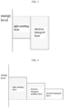
- the material of the electron transport auxiliary layer may be selected so that the electron transport auxiliary layer 331 of the present invention satisfies the following Relational Expression 3 (see FIG. 3 ): HOMO aETL > HOMO EL (in the above formula,
- a difference between an absolute value of the HOMO energy level of the electron transport auxiliary layer 331 and an absolute value of the HOMO energy level of the light-emitting layer 320 may be in a range of greater than 0 eV to 1.0 eV or less.
- the absolute value of the HOMO energy level of the electron transport auxiliary layer 331 is greater than the absolute value of the HOMO energy level of the light-emitting layer 320, holes in the light-emitting layer may be blocked by the energy barrier of the electron transport auxiliary layer and migration to the electron transport auxiliary layer may be prevented, and thus combination of electrons and holes in the light-emitting layer may be increased.
- the material of the electron transport auxiliary layer may be selected so that the electron transport auxiliary layer 331 of the present invention satisfies the following Relational Expression 4 (see FIG. 4 ): LUMO ETL > LUMO aETL > LUMO EL (in the above formula,
- a difference between an absolute value of the LUMO energy level of the electron transport auxiliary layer 331 and an absolute value of the LUMO energy level of the electron transport layer 332 may be in a range of greater than 0 eV to 1.0 eV or less.
- a difference between an absolute value of the LUMO energy level of the electron transport auxiliary layer 331 and an absolute value of the LUMO energy level of the light-emitting layer 320 may be in a range of greater than 0 eV to 1.0 eV or less.
- the LUMO energy level of the electron transport auxiliary layer 331 when the absolute value of the LUMO energy level of the electron transport auxiliary layer 331 is between the absolute value of the LUMO energy level of the electron transport layer 332 and the absolute value of the LUMO energy level of the light-emitting layer 320, the LUMO energy level may have a step arrangement, and electrons injected from the cathode may be smoothly injected from the electron transport layer to the light-emitting layer.
- Any material having physical properties such as the above-described HOMO energy level and LUMO energy level may be used as the electron transport auxiliary layer material of the present invention.
- the material of the electron transport auxiliary layer 331 may be a compound including one or more of moieties represented by the following Chemical Formulas 1 and 2 ("one or more moiety-containing compounds”):
- Chemical Formula 1 when R 1 combines with an adjacent group to form a fused ring, the moiety represented by Chemical Formula 1 may be a moiety represented by Chemical Formula 3, but embodiments are not limited thereto:
- the at least one moiety-containing compound has a high glass transition temperature because a molecular weight of the compound may be significantly increased by controlling various types and introduction positions of the substituents that are introduced into the moieties of Chemical Formulas 1 and 2, and thus thermal stability of the organic EL device may be improved, and there may also be an effect of inhibiting crystallization of the organic layer, and thus durability and lifespan characteristics of the device may be greatly improved.
- the at least one moiety-containing compound may be a compound represented by any one of the following Chemical Formulas 4 to 6 (not according to the present invention ):
- the compound containing one or more moieties described above may be embodied as, but not limited to, compounds 1, 4, 5, 7, 12 not according to the present invention, while compounds 2, 3, 6, 8, 9, 10, 11, 13 and 14 according to the present invention shown below.
- any electron transport material that facilitates electron injection and has high electron mobility may be used as the electron transport layer 332 without limitation.
- the electron transport material may include an oxazole-based compound, an isoxazole-based compound, a triazole-based compound, an isothiazole-based compound, an oxadiazole-based compound, a thiadiazole-based compound, a perylene-based compound, an aluminum complex [e.g., Alq 3 (tris(8-quinolinolato)-aluminium), BAlq, SAlq, Alph 3 , Almq 3 ], a gallium complex (e.g., Gaq'2OPiv, Gaq'2OAc, 2(Gaq'2)) and the like, which may be used solely or in combination of two or more thereof.
- any electron injection material that facilitates electron injection and has high electron mobility may be used without limitation.
- the electron injection material may include LiF, Li 2 O, BaO, NaCl, and CsF; lanthanide metals such as Yb; a metal halide such as RbCl or RbI, and the like, which may be used solely or in combination of two or more thereof.
- the electron transport region 330 according to the present invention may be codeposited with an n-type dopant to facilitate injection of electrons from the cathode.
- an n-type dopant alkali metal complex compounds known in the art may be used without limitation, and examples thereof may include alkali metals, alkaline earth metals, or rare earth metals.
- the electron transport region 330 may be formed through a conventional method known in the art. For example, there may be a vacuum deposition method, a spin coating method, a casting method, a Langmuir-Blodgett (LB) method, an inkjet printing method, a laser printing method, a laser induced thermal imaging (LITI) method, and the like, but embodiments are not limited thereto.
- a vacuum deposition method for example, there may be a vacuum deposition method, a spin coating method, a casting method, a Langmuir-Blodgett (LB) method, an inkjet printing method, a laser printing method, a laser induced thermal imaging (LITI) method, and the like, but embodiments are not limited thereto.
- LB Langmuir-Blodgett
- LITI laser induced thermal imaging
- the organic EL device 100 of the present invention may further include a light-emitting auxiliary layer (not illustrated) disposed between the hole transport region 310 and the light-emitting layer 320.
- a light-emitting auxiliary layer (not illustrated) disposed between the hole transport region 310 and the light-emitting layer 320.
- the light-emitting auxiliary layer serves to control a thickness of the organic layer 300, while transporting holes migrating from the hole transport region 310 to the light-emitting layer 320, or blocking migration of electrons and/or excitons.
- the light-emitting auxiliary layer has a high LUMO value to prevent electrons from migrating to the hole transport layer 312 (or the hole transport auxiliary layer 313), and has a high triplet energy to prevent excitons of the light-emitting layer 320 from being diffused to the hole transport layer 312 (or the hole transport auxiliary layer 313).
- the light-emitting auxiliary layer may include a hole transport material and may include or be formed of a material the same as a material of the hole transport region.
- the light-emitting auxiliary layers of the red, green, and blue organic EL devices may include or be formed of the same material.
- a material for the light-emitting auxiliary layer is not particularly limited, and examples thereof may include carbazole derivatives and arylamine derivatives.
- examples of the light-emitting auxiliary layer may include NPD (N,N-dinaphthyl-N,N'-diphenyl benzidine), TPD (N,N'-bis-(3-methylphenyl)-N,N'-bis(phenyl)-benzidine), s-TAD, MTDATA (4,4',4"-Tris(N-3-methylphenyl-Nphenyl-amino)-triphenylamine), and the like, but embodiments are not limited thereto. These may be used solely or two or more of them may be used in combination with each other.
- the light-emitting auxiliary layer may further include a p-type dopant in addition to the above-described material.
- a p-type dopant in addition to the above-described material.
- any known p-type dopant generally used in the art may be used without particular limitation.
- a content of the p-type dopant may be appropriately adjusted within a range known in the art, for example, in a range of about 0.5 to 50 parts by weight with respect to 100 parts by weight of the hole transport material.
- the light-emitting auxiliary layer may be formed by a vacuum deposition method, a spin coating method, a casting method, a Langmuir-Blodgett (LB) method, an inkjet printing method, a laser printing method, a laser induced thermal imaging (LITI) method, and the like known in the art, but embodiments are not limited thereto.
- a vacuum deposition method a spin coating method, a casting method, a Langmuir-Blodgett (LB) method, an inkjet printing method, a laser printing method, a laser induced thermal imaging (LITI) method, and the like known in the art, but embodiments are not limited thereto.
- LB Langmuir-Blodgett
- LITI laser induced thermal imaging
- the organic EL device 100 of the present invention may further include a capping layer (not illustrated) disposed on the above-described cathode 200.
- the capping layer may serve to allow light generated in the organic layer to be efficiently emitted to the outside while protecting the organic EL device.
- the capping layer may include at least one of tris-8-hydroxyquinoline aluminum (Alq 3 ), ZnSe, 2,5-bis(6'- (2',2"-bipyridyl))-1,1-dimethyl-3,4-diphenylsilole, 4'-bis[N-(1-napthyl)-N- phenyl-amion] biphenyl ( ⁇ -NPD), N,N'-diphenyl-N,N'-bis(3-methylphenyl) -1,1'-biphenyl-4,4'-diamine (TPD), and 1,1'-bis(di-4-tolylaminophenyl) cyclohexane (TAPC).
- the material for forming such a capping layer is inexpensive as compared to materials of other layers of the organic EL device.
- the capping layer may be a single layer, but may include two or more layers having different refractive indices so that the refractive index gradually changes while passing through the two or more layers.
- the capping layer may be prepared by a conventional method known in the art, and for example, various methods such as a vacuum deposition method, a spin coating method, a casting method, or a Langmuir-Blodgett (LB) method may be used.
- various methods such as a vacuum deposition method, a spin coating method, a casting method, or a Langmuir-Blodgett (LB) method may be used.
- the organic EL device according to the present invention has a structure in which the anode 100, the organic layer 300 and the cathode 200 are sequentially stacked.
- an insulating layer (not illustrated) or an adhesive layer (not illustrated) may be further included between the anode 100 and the organic layer 300 or between the cathode 200 and the organic layer 300.
- the organic EL device of the present invention may have excellent lifespan characteristics because a half-life time of initial brightness is increased while maintaining maximum luminous efficiency when voltage and current are applied.
- the organic EL device of the present invention described above may be prepared according to a conventional method known in the art. For example, after vacuum deposition of an anode material on a substrate, a hole transport region material, a light-emitting layer material, an electron transport region material, and a cathode material may be vacuum-deposited on the anode, and thus an organic EL device may be manufactured.
- a HOMO energy level of each compound was measured by cyclic voltammetry (CV) method.
- a glass substrate that had been thin-film-coated with indium tin oxide (ITO) to a thickness of 1500 ⁇ was washed ultrasonically with distilled water. After washing with distilled water was completed, the glass substrate was ultrasonically cleaned with a solvent, such as isopropyl alcohol, acetone and methanol, dried, transferred to a UV OZONE cleaner (Power sonic 405, Hwasin Tech), and cleaned for 5 minutes using UV, and then, the glass substrate was transferred to a vacuum evaporator.
- a solvent such as isopropyl alcohol, acetone and methanol
- DS-205 Doosan Corporation Electro-Materials (80 nm) / NPB (15 nm) / Compound 1 + ADN + 5 % DS-405 (Doosan Corporation Electro-Materials) (30 nm) / Compound 1 (5 nm) / Alq 3 (25 nm) / LiF (1 nm) / Al (200 nm) were stacked in the order, and thus an organic EL device was manufactured.
- the structures ofNPB, ADN, and Alq 3 used are as follows. In such a case, in the light-emitting layer, Compound 1 was used as the first host ('A' in the table 1), and ADN was used as the second host ('B' in the table 1).
- Blue organic EL devices of Embodiments 2 to 14 were manufactured in the same manner as in Embodiment 1, except that each compound ('A') shown in Table 2 was used instead of Compound 1 which is the first host used in the formation of the light-emitting layer of Embodiment 1, and that each compound ('C') shown in Table 2 was used instead of Compound 1 used in the formation of the electron transport auxiliary layer.
- a blue organic EL device was prepared in the same manner as in Embodiment 1, except that Compound 1 which is the first host was not used, and that only ADN which was the second host was used in the formation of the light-emitting layer of Embodiment 1.
- a blue organic EL device was manufactured in the same manner as in Embodiment 1, except that only Compound 1 which is the first host was used and ADN which is the second host was not used in the formation of the light-emitting layer of Embodiment 1, the electron transport auxiliary layer was not formed, and the electron transport layer material Alq 3 was deposited to 30 nm instead of 25 nm.
Landscapes
- Physics & Mathematics (AREA)
- Chemical & Material Sciences (AREA)
- Engineering & Computer Science (AREA)
- Materials Engineering (AREA)
- Spectroscopy & Molecular Physics (AREA)
- Optics & Photonics (AREA)
- Organic Chemistry (AREA)
- Electroluminescent Light Sources (AREA)
Description
- The present invention relates to an organic electroluminescent device simultaneously exhibiting effects such as high luminous efficiency, low driving voltage, and a long lifespan.
- In general, in organic electroluminescent devices ("organic EL devices"), when current or voltage is applied to two electrodes, holes are injected into an organic layer at an anode, and electrons are injected into an organic layer at a cathode. When the injected holes and electrons meet, an exciton is formed, and light is emitted when the exciton falls to the ground state.
- Such organic EL devices may be classified, according to an electron spin type of the formed excitons, into fluorescent EL devices in which singlet excitons contribute to light emission and phosphorescent EL devices in which triplet excitons contribute to light-emission.
- Theoretically, fluorescent EL devices may have an internal quantum efficiency of up to 25%, depending on the generation ratio, whereas phosphorescent EL devices may have an internal quantum efficiency of up to 100%. In the case of phosphorescence, high internal quantum efficiency may be obtained because triplets and singlets are involved in internal quantum efficiency, but in the case of fluorescence, only singlet transition occurs, so the maximum internal quantum efficiency is about a quarter of that of phosphorescence. As such, the phosphorescent EL devices have theoretically higher luminous efficiency than the fluorescence.
- However, unlike green and red phosphorescent EL devices, blue phosphorescent EL devices have not been commercialized due to a low development level of phosphorescent dopants having deep blue color purity and high efficiency and hosts having a wide energy gap. Accordingly, blue fluorescent EL devices are in use instead of the blue phosphorescent EL devices.
- However, the development of organic EL devices having high efficiency and a long lifespan is required in accordance with the recent trend of display enlargement and high resolution. In particular, the high resolution of the display may be realized when more pixels are formed in the same area. For this reason, the light-emitting area of the organic EL devices may decrease, and accordingly, the decrease in the light-emitting area serves as a cause of shortening the life of the organic EL devices.
- Accordingly, various studies have been conducted to improve the characteristics of the organic EL device, but satisfactory results have not been obtained so far.
-
EP3480278A1 relates to a display device comprising an anode; a cathode; and an organic layer disposed between the anode and the cathode and comprising a hole transport region, a light-emitting layer, and an electron transport region sequentially disposed on the anode, wherein the electron transport region comprises an electron transport auxiliary layer, an electron transport layer and an electron injection layer, the light-emitting layer comprises a plurality of hosts and dopants. -
KR101884130B1 -
US2016/149150A1 discloses an organic light-emitting diode including a first electrode, a second electrode, an emitting layer, a hole transport region, a first electron transport region, an interlayer, a second electron transport region. -
KR2018 0072245A -
KR20190088651A - The present invention is directed to an organic electroluminescent device in which a light-emitting layer includes a plurality of hosts and dopants, where one of the plurality of hosts includes the same material as in an electron transport auxiliary layer, whereby the organic electroluminescent device exhibits effects such as low driving voltage, high luminous efficiency, and a long lifespan.
- The present invention provides an organic electroluminescent device including: an anode; a cathode disposed opposing the anode; and an organic layer disposed between the anode and the cathode and comprising a hole transport region, a light-emitting layer, and an electron transport region sequentially disposed on the anode, wherein the electron transport region comprises an electron transport auxiliary layer, an electron transport layer and an electron injection layer sequentially disposed on the light-emitting layer, the light-emitting layer comprises a plurality of hosts and dopants, and one of the plurality of hosts comprises a material the same as a material of the electron transport auxiliary layer.
- The present invention provides an organic electroluminescent device in which a light-emitting layer includes a plurality of hosts and dopants, where one of the plurality of hosts includes the same material as in an electron transport auxiliary layer, whereby the organic electroluminescent device exhibits effects such as low driving voltage, high luminous efficiency, and a long lifespan.
- The present invention further provides a display panel with improved performance and lifespan by applying the organic electroluminescent device of the present invention to the display panel.
-
-
FIG. 1 is a cross-sectional view illustrating a structure of an organic electroluminescent ("EL") device according to an embodiment of the present invention. -
FIG. 2 is a cross-sectional view illustrating a structure of an organic EL device according to another embodiment of the present invention. -
FIG. 3 is a graph illustrating relationship of a highest occupied molecular orbital ("HOMO") energy level between a light-emitting layer and an electron transport auxiliary layer according to an embodiment of the present invention. -
FIG. 4 is a graph illustrating relationship of a lowest unoccupied molecular orbital ("LUMO") energy level between a light-emitting layer, an electron transport auxiliary layer, and an electron transport layer according to an embodiment of the present invention. -
- 100: anode, 200: cathode,
- 300: organic layer, 310: hole transport region,
- 311: hole injection layer, 312: hole transport layer,
- 313: hole transport auxiliary layer, 320: light-emitting layer,
- 330: electron transport region, 331: electron transport auxiliary layer;
- 332: electron transport layer, 333: electron injection layer
- Advantages and features of the present invention and methods for achieving them will become apparent with reference to embodiments described below in detail in conjunction with the accompanying drawings. However, the present invention is not limited to the embodiments disclosed below but may be implemented in various different forms, and it is to be understood that the present embodiments are merely provided to make the disclosure of the present invention complete and to fully convey the scope of the present invention to those of ordinary skill in the art, and the present invention is defined only by the scope of the claims. Thus, in some embodiments, well-known process steps, well-known device structures and well-known techniques are not described in detail in order to avoid obscuring the present invention. Like reference numerals refer to like elements throughout the specification.
- Unless otherwise defined, all terms used in the present specification (including technical and scientific terms) may be used with meanings that may be commonly understood by those skilled in the art. In addition, the terms defined in the commonly used dictionaries are not ideally or excessively interpreted, unless they are specifically defined clearly.
- An organic electroluminescent ("EL") device according to the present invention includes: an anode; a cathode disposed opposing the anode; and one or more organic layers disposed between the anode and the cathode and including a hole transport region, a light-emitting layer, and an electron transport region, where the same material as in an electron transport auxiliary layer in the electron transport region is used in one of a plurality of hosts in the light-emitting layer, wherein a material for the electron transport auxiliary layer is defined in claim 1.
- Accordingly, the organic EL device of the present invention may have characteristics such as a low driving voltage, a high luminous efficiency and a long lifespan.
- Specifically, in the organic EL device of the present invention, the light-emitting layer includes a plurality of hosts, for example, a first host and a second host different from each other, to prevent reverse transfer phenomenon in which exciton transferred from the host to the dopant is transferred back to the host, while improving recombination efficiency of the holes and electrons.
- In such a case, an electron transport auxiliary layer may be disposed between the light-emitting layer and the electron transport layer, and one of the plurality of hosts may include a material the same as a material of the electron transport auxiliary layer, such that an electron injection barrier between the light-emitting layer and the electron transport layer may be lowered, and barrier-free effects between the light-emitting layer and the electron transport auxiliary layer may be exhibited, thereby allowing electrons injected from the electron transport layer to be smoothly supplied to the light-emitting layer through the electron transport auxiliary layer. Accordingly, in the organic EL device of the present invention, luminous efficiency may be enhanced, a driving voltage may be lowered, and lifespan characteristics may be significantly improved.
- Hereinafter, embodiments of the organic EL device according to the present invention will be described with reference to the accompanying drawings. However, embodiment of the present invention may be modified into various other forms, and the scope of the present invention is not limited to the embodiments described below.
-
FIG. 1 is a cross-sectional view illustrating a structure of an organic electroluminescent ("EL") device according to an embodiment of the present invention.FIG. 2 is a cross-sectional view illustrating a structure of an organic EL device according to another embodiment of the present invention. - Referring to
FIGS. 1 and 2 , the organic EL device sequentially includes ananode 100, one or moreorganic layers 300, and acathode 200, and theorganic layer 300 includes ahole transport region 310, a light-emitting layer 320, and anelectron transport region 330. Optionally, the organic EL device may further include a capping layer (not illustrated) disposed on thecathode 200. - Hereinafter, each structure of the organic EL device according to the present invention will be described in detail.
- The organic EL device of the present invention includes the
anode 100. Theanode 100 may be disposed on a substrate and electrically connected to a driving thin film transistor ("TFT") to receive a driving current from the driving thin film transistor. Since theanode 100 includes or is formed of a material having a relatively high work function, it may inject holes into an adjacent one of the organic layers, that is, the hole transport region 310 (e.g., a hole injection layer 311). - A material for forming the anode is not particularly limited, and a conventional one known in the art may be used. Examples thereof may include metals, such as vanadium, chromium, copper, zinc, and gold; alloys thereof; metal oxides such as zinc oxide, indium oxide, indium tin oxide (ITO), and indium zinc oxide (IZO); combinations of metals and oxides such as ZnO:Al and SnO2:Sb; conductive polymers such as polythiophene, poly(3-methylthiophene), poly[3,4-(ethylene-1,2-dioxy)thiophene] (PEDT), polypyrrole, and polyaniline; and carbon black, but embodiments are not limited thereto.
- A method of preparing the anode is not particularly limited, and may be prepared through a conventional method known in the art. For example, the anode may be formed by coating the anode material on a substrate through a known thin film forming method such as a sputtering method, an ion plating method, a vacuum deposition method, or a spin coating method.
- The substrate may be a plate-shaped member for supporting the organic EL device, and include, for example, a silicon wafer, quartz, a glass plate, a metal plate, a plastic film, and a sheet, but embodiments are not limited thereto.
- In the organic EL device of the present invention, the
cathode 200 is disposed opposing the anode, and specifically, disposed on theelectron transport region 330. Since thecathode 200 includes or is formed of a material having a relatively low work function, it may inject electrons into an adjacent one of the organic layers, that is, the electron transport region 330 (e.g., an electron injection layer 333). - A material for forming the cathode is not particularly limited, and a conventional one known in the art may be used. Examples thereof may include metals, such as magnesium, calcium, sodium, potassium, titanium, indium, yttrium, lithium, gadolinium, aluminum, silver (Ag), tin, and lead; alloys thereof; and a multi-layer structure material such as LiF/Al or LiO2/Al, but embodiments are not limited thereto.
- A method of preparing the cathode is not particularly limited, and similar to the anode, the cathode may be prepared through a conventional method known in the art. For example, the cathode may be formed by coating the cathode material on the one or more
organic layers 300, specifically on the electron transport region, for example, theelectron injection layer 333, through the above-described thin film forming method. - In the organic EL device of the present invention, the one or more
organic layers 300 are disposed between theanode 100 and thecathode 200. - The
organic layer 300 includes thehole transport region 310, the light-emittinglayer 320, and theelectron transport region 330. - According to an embodiment, as illustrated in
FIG. 1 , the one or moreorganic layers 300 may include ahole injection layer 311, ahole transport layer 312, a hole transportauxiliary layer 313, a light-emittinglayer 320, an electron transportauxiliary layer 331, anelectron transport layer 332, and anelectron injection layer 333 sequentially disposed on theanode 100. - According to another embodiment, as illustrated in
FIG. 2 , the one or moreorganic layers 300 may include ahole injection layer 311, ahole transport layer 312, a hole transportauxiliary layer 313, a light-emittinglayer 320, an electron transportauxiliary layer 331, anelectron transport layer 332, and anelectron injection layer 333 sequentially disposed on theanode 100. - Hereinafter, each organic layer will be described.
- In the
organic EL device 100 of the present invention, thehole transport region 310 is a portion of theorganic layer 300 disposed on theanode 100, and serves to allow holes injected from theanode 100 to migrate into another adjacent one of the organic layers, specifically to the light-emittinglayer 320. Thehole transport region 310 may include at least one of thehole injection layer 311, thehole transport layer 312, and the hole transportauxiliary layer 313. - For example, as illustrated in
FIG. 1 , thehole transport region 310 may include thehole injection layer 311 and thehole transport layer 312 sequentially stacked on theanode 100. - As another example, as illustrated in
FIG. 2 , thehole transport region 310 may include thehole injection layer 311, thehole transport layer 312, and the hole transportauxiliary layer 313 sequentially stacked on theanode 100. - A material forming the
hole injection layer 311 and thehole transport layer 312 of the present invention is not particularly limited as long as it has a low hole injection barrier and a high hole mobility, and any material for the hole injection/transport layer may be used without limitation. In such a case, respective materials for forming thehole injection layer 311 and thehole transport layer 312 may be the same or different from each other. - Specifically, the
hole injection layer 311 may include a hole injection material known in the art. Non-limiting examples of the hole injection material may include phthalocyanine compounds such as copper phthalocyanine; DNTPD (N,N'-diphenyl-N,N'-bis-[4-(phenyl-m-tolyl-amino)-phenyl]-biphenyl-4,4'-diamine), m-MTDATA (4,4',4"-tris(3-methylphenylphenylamino) triphenylamine), TDATA (4,4'4"-Tris(N,N-diphenylamino)triphenylamine), 2TNATA (4,4',4"-tris{N,-(2-naphthyl)-N-phenylamino}-triphenylamine), PEDOT/PSS (poly(3,4-ethylenedioxythiophene)/poly(4-styrenesulfonate)), PANI/DBSA (polyaniline/dodecylbenzenesulfonic acid), PANI/CSA (polyaniline/Camphor sulfonicacid), PANI/PSS ((polyaniline)/poly(4-styrenesulfonate)), and the like, which may be used solely or in combination of two or more thereof. - The
hole transport layer 312 includes a hole transport material known in the art. Non-limiting examples of the hole transport material may include carbazole-based derivatives such as N-phenylcarbazole and polyvinylcarbazole; fluorene-based derivatives, amine-based derivatives; triphenylamine-based derivatives such as TPD (N,N'-bis(3-methylphenyl)-N,N'-diphenyl-[1,1-biphenyl]-4,4'-diamine) and TCTA (4,4',4"-tris(N-carbazolyl)triphenylamine); NPB (N,N'-di(1-naphthyl)-N,N'-diphenylbenzidine), TAPC (4,4'-cyclohexylidene bis[N,N-bis(4-methylphenyl)benzenamine]), and the like, which may be used solely or in combination of two or more thereof. - The hole transport
auxiliary layer 313 may prevent electrons or excitons generated in the light-emittinglayer 320 from diffusing (migrating) into thehole transport region 310. A material of the hole transportauxiliary layer 313 may be used without limitation as long as it has general hole transport properties known in the art, and may be, for example, the above-described hole transport material. - The
hole transport region 310 may be formed through a conventional method known in the art. For example, there may be a vacuum deposition method, a spin coating method, a casting method, a Langmuir-Blodgett (LB) method, an inkjet printing method, a laser printing method, a laser induced thermal imaging (LITI) method, and the like, but embodiments are not limited thereto. - In the organic EL device of the present invention, the light-emitting
layer 320 is a portion of theorganic layer 300 disposed between theanode 100 and thecathode 200, and specifically disposed on thehole transport region 320. Specifically, the light-emittinglayer 320 may be disposed on thehole transport layer 312 or on the hole transport auxiliary layer 313 (seeFIGS. 1 and 2 ). The light-emittinglayer 320 is a layer in which holes and electrons injected from the anode and the cathode, respectively, are combined to form excitons, and a color of light emitted by the organic EL device may vary depending on the material forming the light-emittinglayer 320. - The light-emitting
layer 320 of the present invention includes a plurality of hosts and dopants. In such a case, one of the plurality of hosts is (e.g., is or includes) a material the same as (e.g., identical to) a material included in or forming the electron transport auxiliary layer ("electron transport auxiliary layer material"). - According to an embodiment, the plurality of hosts may include: a first host that is the same as the electron transport auxiliary layer material; and a second host different from the first host. As such, when one of the plurality of hosts is the same as the electron transport auxiliary layer material, barrier-free effects may be exhibited between the light-emitting layer and the electron transport auxiliary layer, thereby realizing a low driving voltage, a high luminous efficiency and a long lifespan of the device.
- The first host of the present invention is a material the same as a material of the electron transport auxiliary layer. Specifically, the first host may be a compound including at least one of moieties represented by the following Chemical Formulas A-1 to A-16. For example, the first host may be a compound represented by any one of the following Chemical Formulas B-1 to B-9.
- According to an embodiment the first host (not according to the invention) may be one of the following compounds 1, 4, 5, 7, 12; while the first host (according to the invention) may be one of the following compounds 2, 3, 6, 8, 9, 10, 11, 13 and 14.
- A detailed description of these compounds will be described below in a section of the electron transport auxiliary layer.
- The second host of the present invention is a host different from the first host, any host known in the art may be used without particular limitation, and non-limiting examples thereof may include alkali metal complex compounds; alkaline earth metal complex compounds; or aromatic ring-fused derivatives. Specifically, examples of the second host may include aluminum complex compounds, beryllium complex compounds, iridium compounds, anthracene derivatives, pyrene derivatives, triphenylene derivatives, carbazole derivatives, dibenzofuran derivatives, dibenzothiophene derivatives, fluorene derivatives, nitrogen-containing heterocyclic derivatives, or a combination of one or more thereof which may enhance luminous efficiency and lifespan of the organic EL device.
- However, in the present invention, in order to prevent reverse transfer phenomenon of excitons, while significantly increasing the number of excitons in the light-emitting layer, in selecting the second host, differences in physical properties such as a HOMO energy level difference or a LUMO energy level difference with respect to the first host needs to be considered.
- According to an embodiment, the second host may be a material satisfying the following Relational Expressions 1 and 2:


- LUMOhost-1 is a LUMO energy level of the first host,
- LUMOhost-2 is a LUMO energy level of the second host,
- HOMOhost-1 is a HOMO energy level of the first host, and
- HOMOhost-2 is a HOMO energy level of the second host.
- Specifically, a difference between an absolute value of the LUMO energy level of the second host and an absolute value of the LUMO energy level of the first host may be in a range of greater than 0 eV to 1.0 eV or less, and a difference between an absolute value of the HOMO energy level of the second host and an absolute value of the HOMO energy level of the first host may be in a range of greater than 0 eV to 1.0 eV or less.
- A content of hosts (e.g., the first host) that are the same as the electron transport auxiliary layer material from among the plurality of hosts may be in a range of 30 to 90 percent by weight (wt%) with respect to the total amount of entire hosts. For example, when the plurality of hosts include the first host which is the same as the electron transport auxiliary layer material and the second host different from the first host, a use ratio of the first host and the second host is not particularly limited, and for example, the ratio may be in a range of 30:70 to 90:10 by weight. If the use ratio of the first host and the second host is within the above ratio, the dopant-to-host exciton reverse transfer phenomenon may be more effectively prevented, while achieving increased barrier-free effects between the light-emitting layer and the electron transport auxiliary layer.
- Optionally, the light-emitting layer of the present invention may further include one or more other hosts (e.g., a third host) different from the first and second hosts described above. In such a case, an example of the third host may be the same as the examples of the second host, and thus description thereof will be omitted.
- In the light-emitting layer of the present invention, any dopant commonly known in the art may be used as the dopant without particular limitation. Such dopants may be classified into fluorescent dopants and phosphorescent dopants, and the phosphorescent dopant may be an organometallic complex including Ir, Pt, Os, Re, Ti, Zr, Hf, or a combination of two or more thereof, but embodiments are not limited thereto.
- In an embodiment, the dopant may be classified into red dopants, green dopants, and blue dopants, and red dopants, green dopants, and blue dopants commonly known in the art may be used without particular limitation.
- Specifically, non-limiting examples of the red dopant may include PtOEP (Pt(II) octaethylporphine), Ir(piq)3 (tris(2-phenylisoquinoline)iridium), Btp2Ir(acac) (bis(2-(2'-benzothienyl)-pyridinato-N,C3')iridium(acetylacetonate), and the like, which may be used solely or in combination of two or more thereof.
- In addition, non-limiting examples of the green dopant may include Ir(ppy)3 (tris(2-phenylpyridine) iridium), Ir(ppy)2(acac) (bis(2-phenylpyridine)(Acetylacetonato)iridium(III)), Ir(mppy)3 (tris(2-(4-tolyl)phenylpiridine)iridium), C545T (10-(2-benzothiazolyl)-1,1,7,7-tetramethyl-2,3,6,7-tetrahydro-1H,5H,11H-[1]benzopyrano [6,7,8-ij]-quinolizin-11-one, and the like, which may be used solely or in combination of two or more thereof.
- In addition, non-limiting examples of the blue dopant may include F2Irpic (bis[3,5-difluoro-2-(2-pyridyl)phenyl](picolinato)iridium(III)), (F2ppy)2Ir(tmd), Ir(dfppz)3, DPVBi (4,4'-bis(2,2'-diphenylethen-1-yl)biphenyl), DPAVBi (4,4'-Bis[4-(diphenylamino)styryl]biphenyl), TBPe (2,5,8,11-tetra-tert-butyl perylene), and the like, which may be used solely or in combination of two or more thereof.
- Contents of the dopants are not particularly limited and may be appropriately adjusted within a range known in the art.
- For example, the plurality of hosts and the plurality of dopants may be included with a weight ratio in a range of 70:30 to 99.9:0.1 with respect to the total amount of the light-emitting layer. Specifically, when the light-emitting
layer 320 is blue fluorescent, green fluorescent, or red fluorescent, the plurality of hosts and the plurality of dopants may be included with a weight ratio in a range of 80:20 to 99.9:0.1. In addition, when the light-emittinglayer 320 is blue fluorescent, green fluorescent, or red phosphorescent, the plurality of hosts and the plurality of dopants may be included with a weight ratio in a range of 70:30 to 99:1. - In another example, the content of the dopant may be in a range of about 0 to 30 parts by weight, specifically more than 0 parts by weight to 20 pats by weight or less, more specifically in a range of about 0.1 to 15 parts by weight, with respect to 100 parts by weight of the total amount of the first hosts and the second hosts.
- The above-described light-emitting
layer 320 may be a single layer or may be formed of a plurality of layers of two or more layers. In such a case, when the light-emittinglayer 320 includes a plurality of layers, the organic EL device may emit light of various colors. Specifically, the present invention may provide an organic EL device having a mixed color by providing, in series, a plurality of light-emitting layers including or formed of heterogeneous materials. In addition, when including the plurality of light-emitting layers, a driving voltage of the device may increase, while a current value in the organic EL device becomes constant, and accordingly, it is possible to provide an organic EL device with improved luminous efficiency by the number of light-emitting layers. - The light-emitting
layer 320 may be formed through a conventional method known in the art. For example, there may be a vacuum deposition method, a spin coating method, a casting method, a Langmuir-Blodgett (LB) method, an inkjet printing method, a laser printing method, a laser induced thermal imaging (LITI) method, and the like, but embodiments are not limited thereto. For example, the light-emitting layer may be formed by co-deposition of the plurality of hosts (e.g., a first host and a second host) mixed with each other. - In the organic EL device according to the present invention, the
electron transport region 330 is an organic layer disposed on the light-emittinglayer 320, and allows electrons injected from thecathode 200 to migrate to the light-emittinglayer 320. - The
electron transport region 330 includes the electron transportauxiliary layer 331, theelectron transport layer 332, and theelectron injection layer 333 sequentially disposed on the light-emittinglayer 320. - The electron transport
auxiliary layer 331 according to the present invention facilitates migration of electrons from theelectron transport layer 332 to the light-emittinglayer 320, and prevents excitons generated in the light-emittinglayer 320 or holes injected into the light-emittinglayer 320 from being diffused (e.g., migrating) to theelectron transport layer 332. A material for forming the electron transportauxiliary layer 331 is also not particularly limited as long as it has a low electron injection barrier and high electron mobility, and any material known in the art may be used without particular limitation. - However, in the present invention, in order to achieve barrier-free effects between the light-emitting layer and the electron transport auxiliary layer, a material of the electron transport auxiliary layer may be the same as one of the plurality of hosts (e.g., the first host) in the light-emitting layer. In particular, the electron transport auxiliary layer may be formed by using a host having a low electron injection barrier and a high electron mobility from among the plurality of hosts in the light-emitting layer. Accordingly, in the organic EL device of the present invention, electrons injected from the electron transport layer may be smoothly supplied to the light-emitting layer through the electron transport auxiliary layer, such that a combination rate between holes and electrons may be increased, and thus the number of excitons may be significantly increased. Accordingly, the organic EL device of the present invention may exhibit high-efficiency luminous characteristics, and furthermore, as the driving voltage is lowered, life-span characteristics may be significantly improved.
- In such a case, in order to achieve the barrier-free effects between the electron transport
auxiliary layer 331 and the light-emittinglayer 320 as well as to lower the electron injection barrier between the electron transportauxiliary layer 331 and theelectron transport layer 332, a material of the electron transportauxiliary layer 331 needs to be selected in consideration of physical properties such as a difference in HOMO energy level or a difference in LUMO energy level between the electron transportauxiliary layer 331, theelectron transport layer 332, and the light-emittinglayer 320. - According to an embodiment, the material of the electron transport auxiliary layer may be selected so that the electron transport
auxiliary layer 331 of the present invention satisfies the following Relational Expression 3 (seeFIG. 3 ):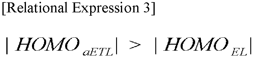
- HOMOaETL is a HOMO energy level of the electron transport auxiliary layer, and
- HOMOEL is a HOMO energy level of the light-emitting layer).
- Specifically, a difference between an absolute value of the HOMO energy level of the electron transport
auxiliary layer 331 and an absolute value of the HOMO energy level of the light-emittinglayer 320 may be in a range of greater than 0 eV to 1.0 eV or less. - As such, when the absolute value of the HOMO energy level of the electron transport
auxiliary layer 331 is greater than the absolute value of the HOMO energy level of the light-emittinglayer 320, holes in the light-emitting layer may be blocked by the energy barrier of the electron transport auxiliary layer and migration to the electron transport auxiliary layer may be prevented, and thus combination of electrons and holes in the light-emitting layer may be increased. - According to another embodiment, the material of the electron transport auxiliary layer may be selected so that the electron transport
auxiliary layer 331 of the present invention satisfies the following Relational Expression 4 (seeFIG. 4 ):
- LUMOETL is a LUMO energy level of the electron transport layer,
- LUMOaETL is a LUMO energy level of the electron transport auxiliary layer, and
- LUMOEL is a LUMO energy level of the light-emitting layer).
- Specifically, a difference between an absolute value of the LUMO energy level of the electron transport
auxiliary layer 331 and an absolute value of the LUMO energy level of theelectron transport layer 332 may be in a range of greater than 0 eV to 1.0 eV or less. In addition, a difference between an absolute value of the LUMO energy level of the electron transportauxiliary layer 331 and an absolute value of the LUMO energy level of the light-emittinglayer 320 may be in a range of greater than 0 eV to 1.0 eV or less. - As such, when the absolute value of the LUMO energy level of the electron transport
auxiliary layer 331 is between the absolute value of the LUMO energy level of theelectron transport layer 332 and the absolute value of the LUMO energy level of the light-emittinglayer 320, the LUMO energy level may have a step arrangement, and electrons injected from the cathode may be smoothly injected from the electron transport layer to the light-emitting layer. - Any material having physical properties such as the above-described HOMO energy level and LUMO energy level may be used as the electron transport auxiliary layer material of the present invention.
- For example, the material of the electron transport auxiliary layer 331 (not according to the present invention) may be a compound including one or more of moieties represented by the following Chemical Formulas 1 and 2 ("one or more moiety-containing compounds"):


- where in Chemical Formulas 1 and 2,
- X1 to X6 may be the same as or different from each other, each independently being N or C(R1), where at least one of X1 to X6 (specifically, one to three of X1 to X6) may be N, and when C(R1) is plural in number, the plurality of R1 may be the same as or different from each other,
- Y1 to Y5 may be the same as or different from each other, each independently being N or C(R2), where at least one of Y1 to Y5 (specifically, one to three of Y1 to Y5) may be N, and when C(R2) is plural in number, the plurality of R2 may be the same as or different from each other,
- R1 and R2 may be the same as or different from each other, each independently being selected from: hydrogen, deuterium, a halogen group, a cyano group, a nitro group, an amino group, a C1 to C40 alkyl group, a C2 to C40 alkenyl group, a C2 to C40 alkynyl group, a C3 to C40 cycloalkyl group, a heterocycloalkyl group having 3 to 40 nuclear atoms, a C6 to C60 aryl group, a heteroaryl group having 5 to 60 nuclear atoms, a C1 to C40 alkyloxy group, a C6 to C60 aryloxy group, a C1 to C40 alkylsilyl group, a C6 to C60 arylsilyl group, a C1 to C40 alkylboron group, a C6 to C60 arylboron group, a C6 to C60 arylphosphine group, a C6 to C60 arylphosphine oxide group and a C6 to C60 arylamine group, or forming a fused ring (e.g., a condensed ring) with an adjacent group, and
- the alkyl group, the alkenyl group, the alkynyl group, the aryl group, the heteroaryl group, the aryloxy group, the alkyloxy group, the cycloalkyl group, the heterocycloalkyl group, the arylamine group, the alkylsilyl group, the alkylboron group, the arylboron group, the phosphine group, and the phosphine oxide group of R1 and R2 may each be independently substituted or unsubstituted with one or more substituents of: hydrogen, deuterium (D), a halogen group, a cyano group, a nitro group, a C1 to C40 alkyl group, a C2 to C40 alkenyl group, a C2 to C40 alkynyl group, a C3 to C40 cycloalkyl group, a heterocycloalkyl group having 3 to 40 nuclear atoms, a C6 to C60 aryl group, a heteroaryl group having 5 to 60 nuclear atoms, a C1 to C40 alkyloxy group, a C6 to C60 aryloxy group, a C1 to C40 alkylsilyl group, a C6 to C60 arylsilyl group, a C1 to C40 alkylboron group, a C6 to C60 arylboron group, a C6 to C60 arylphosphine group, a C6 to C60 arylphosphine oxide group and a C6 to C60 arylamine group, and when the substituents are plural in number, the substituents may be the same as or different from each other.
- In Chemical Formula 1, when R1 combines with an adjacent group to form a fused ring, the moiety represented by Chemical Formula 1 may be a moiety represented by Chemical Formula 3, but embodiments are not limited thereto:

- where in Chemical Formula 3,
- X1 to X6 may be the same as those defined in Chemical Formula 1 above, respectively,
- Z1 to Z3 may be the same as or different from each other, each independently being N or C(R3), where at least one of Z1 to Z3 (specifically, one or two of Z1 to Z3) is N, and when C(R3) is plural in number, the plurality of R3 are the same as or different from each other,
- R3 may be selected from: hydrogen, deuterium, a halogen group, a cyano group, a nitro group, an amino group, a C1 to C40 alkyl group, a C2 to C40 alkenyl group, a C2 to C40 alkynyl group, a C3 to C40 cycloalkyl group, a heterocycloalkyl group having 3 to 40 nuclear atoms, a C6 to C60 aryl group, a heteroaryl group having 5 to 60 nuclear atoms, a C1 to C40 alkyloxy group, a C6 to C60 aryloxy group, a C1 to C40 alkylsilyl group, a C6 to C60 arylsilyl group, a C1 to C40 alkylboron group, a C6 to C60 arylboron group, a C6 to C60 arylphosphine group, a C6 to C60 arylphosphine oxide group and a C6 to C60 arylamine group, or may form a fused ring with an adjacent group, and
- the alkyl group, the alkenyl group, the alkynyl group, the aryl group, the heteroaryl group, the aryloxy group, the alkyloxy group, the cycloalkyl group, the heterocycloalkyl group, the arylamine group, the alkylsilyl group, the alkylboron group, the arylboron group, the phosphine group, and the phosphine oxide group of R3 may be substituted or unsubstituted with one or more substituents of: hydrogen, deuterium, a halogen group, a cyano group, a nitro group, a C1 to C40 alkyl group, a C2 to C40 alkenyl group, a C2 to C40 alkynyl group, a C3 to C40 cycloalkyl group, a heterocycloalkyl group having 3 to 40 nuclear atoms, a C6 to C60 aryl group, a heteroaryl group having 5 to 60 nuclear atoms, a C1 to C40 alkyloxy group, a C6 to C60 aryloxy group, a C1 to C40 alkylsilyl group, a C6 to C60 arylsilyl group, a C1 to C40 alkylboron group, a C6 to C60 arylboron group, a C6 to C60 arylphosphine group, a C6 to C60 arylphosphine oxide group and a C6 to C60 arylamine group, and when the substituents are plural in number, the substituents may be the same as or different from each other.
- The at least one moiety-containing compound described above has an electron withdrawing group ("EWG") property in which the moieties of Chemical Formulas 1 and 2 have high electron absorbable properties. Accordingly, when the at least one moiety-containing compound is applied as materials of both of the electron transport auxiliary layer and one of the plurality of hosts of the light-emitting layer, electrons injected from the cathode may be smoothly supplied from the electron transport layer to the light-emitting layer, and accordingly, the driving voltage of the organic EL device may be lowered, and high efficiency and long lifespan may be induced.
- In addition, the at least one moiety-containing compound has a high glass transition temperature because a molecular weight of the compound may be significantly increased by controlling various types and introduction positions of the substituents that are introduced into the moieties of Chemical Formulas 1 and 2, and thus thermal stability of the organic EL device may be improved, and there may also be an effect of inhibiting crystallization of the organic layer, and thus durability and lifespan characteristics of the device may be greatly improved.
- Specifically, the at least one moiety-containing compound may be a compound represented by any one of the following Chemical Formulas 4 to 6 (not according to the present invention ):


- where in Chemical Formulas 4 to 6,
- X1 to X6, Y1 to Y4, and Z1 and Z3 may be the same as those defined in Chemical Formulas 1 to 3, respectively,
- L1 to L3 may be the same or different from each other, each independently being a single bond, or being selected from a C6 to C18 arylene group and a heteroarylene group having 5 to 18 nuclear atoms, specifically selected from: a single bond, a phenylene group, a biphenylene group, a terphenylene group, a divalent naphthyl group, a divalent phenanthryl group, a divalent anthracene group, a divalent pyrene group, a divalent chrysene group, a divalent carbazole group, a divalent dibenzofuran group, a divalent dibenzothiophene group, a divalent fluorene group, a divalent fluorancene group, a divalent triphenylene group, a divalent furan group, a divalent indole group, a divalent indene group, a divalent thiophene group, a divalent benzofuran group, a divalent benzothiophene group, a divalent benzoindene group, and combinations of two or more thereof, and
- Ar1 to Ar3 may be the same as or different from each other, each independently being a substituent selected from the following Chemical Formulas S1 to S9:


- in Chemical Formulas S1 to S9,
- A1 and A2 may be N or CR17,
- A3 and A4 may be the same as or different from each other, each independently being a single bond, or being selected from: NR18, O, S, and CR19R20, wherein a case where both of A3 and A4 are single bonds is excluded,
- A5 to A9 may be N or CR21, where at least one of A5 to A9 (specifically, one to three of A5 to A9) is N, and when CR21 is plural in number, the plurality of R21 are the same as or different from each other,
- A10 to A13 may be N or CR22, where at least one of A10 to A13 (specifically, one to three of A10 to A13) is N, and when CR22 is plural in number, the plurality of R22 are the same as or different from each other,
- A14 to A21 may be N or CR23, where at least one of A14 to A21 (specifically, one to four of A14 to A21) is N, and when CR23 is plural in number, the plurality of R23 are the same as or different from each other,
- a, b, c, d, e, f, h, k, and l may each be an integer in a range of 0 to 4;
- g and j may each be an integer in a range of 0 to 3,
- i and m may each be an integer in a range of 0 to 9,
- R4 to R23 may be the same as or different from each other, each independently being selected from: hydrogen, deuterium, a halogen group, a cyano group, a nitro group, an amino group, a C1 to C40 alkyl group, a C2 to C40 alkenyl group, a C2 to C40 alkynyl group, a C3 to C40 cycloalkyl group, a heterocycloalkyl group having 3 to 40 nuclear atoms, a C6 to C60 aryl group, a heteroaryl group having 5 to 60 nuclear atoms, a C1 to C40 alkyloxy group, a C6 to C60 aryloxy group, a C1 to C40 alkylsilyl group, a C6 to C60 arylsilyl group, a C1 to C40 alkylboron group, a C6 to C60 arylboron group, a C6 to C60 arylphosphine group, a C6 to C60 arylphosphine oxide group and a C6 to C60 arylamine group, or forming a fused ring with an adjacent group, and
- the alkyl group, the alkenyl group, the alkynyl group, the aryl group, the heteroaryl group, the aryloxy group, the alkyloxy group, the cycloalkyl group, the heterocycloalkyl group, the arylamine group, the alkylsilyl group, the alkylboron group, the arylboron group, the phosphine group, and the phosphine oxide group of R4 to R23 may each independently be substituted or unsubstituted with one or more substituents of: hydrogen, deuterium, a halogen group, a cyano group, a nitro group, a C1 to C40 alkyl group, a C2 to C40 alkenyl group, a C2 to C40 alkynyl group, a C3 to C40 cycloalkyl group, a heterocycloalkyl group having 3 to 40 nuclear atoms, a C6 to C60 aryl group, a heteroaryl group having 5 to 60 nuclear atoms, a C1 to C40 alkyloxy group, a C6 to C60 aryloxy group, a C1 to C40 alkylsilyl group, a C6 to C60 arylsilyl group, a C1 to C40 alkylboron group, a C6 to C60 arylboron group, a C6 to C60 arylphosphine group, a C6 to C60 arylphosphine oxide group and a C6 to C60 arylamine group, and when the substituents are plural in number, the substituents may be the same as or different from each other.
- Specifically, the compound represented by any one of the above Chemical Formulas 4 to 6 may be one of compounds represented by the following Chemical Formulas A-1 to A- 16, (according to the present invention) but embodiments are not limited thereto:






- where in Chemical Formulas A-1 to A-16,
- R1 and R2 may be the same as those defined in Chemical Formulas 1 to 3, respectively,
- L1 to L3 and Ar1 to Ar3 may be the same as those defined in Chemical Formulas 4 to 6, respectively,
- n1 and n6 may each be an integer in a range of 0 to 4,
- n2, n3, n4, and n7 may each be an integer in a range of 0 to 3, and
- n5 and n8 may each be an integer in a range of 0 to2.
- More specifically, the compound represented by any one of Chemical Formulas 4 to 6 may selected from compounds represented by the following Chemical Formulas B-1 to B-9, but embodiments are not limited thereto:



- where in the above Chemical Formulas B-1 to B-9,
- X1, X3, X5, and R1 may be the same as those defined in Chemical Formulas 1 to 3, respectively,
- L1 and L3 may be the same as those defined in Chemical Formulas 4 to 6, respectively,
- A1 to A5, A7, A9, R4 to R16, R21, R23, a to h may be the same as those defined in Chemical Formulas S1 to S9, respectively, and
- n6 and n7 may be the same as those defined in Chemical Formulas A-1 to A-16, respectively.
- The compound containing one or more moieties described above may be embodied as, but not limited to, compounds 1, 4, 5, 7, 12 not according to the present invention, while compounds 2, 3, 6, 8, 9, 10, 11, 13 and 14 according to the present invention shown below.

- In the
electron transport region 330 according to the present invention, any electron transport material that facilitates electron injection and has high electron mobility may be used as theelectron transport layer 332 without limitation. Non-limiting examples of the electron transport material may include an oxazole-based compound, an isoxazole-based compound, a triazole-based compound, an isothiazole-based compound, an oxadiazole-based compound, a thiadiazole-based compound, a perylene-based compound, an aluminum complex [e.g., Alq3 (tris(8-quinolinolato)-aluminium), BAlq, SAlq, Alph3, Almq3], a gallium complex (e.g., Gaq'2OPiv, Gaq'2OAc, 2(Gaq'2)) and the like, which may be used solely or in combination of two or more thereof. - In addition, as the
electron injection layer 333, any electron injection material that facilitates electron injection and has high electron mobility may be used without limitation. Non-limiting examples of the electron injection material may include LiF, Li2O, BaO, NaCl, and CsF; lanthanide metals such as Yb; a metal halide such as RbCl or RbI, and the like, which may be used solely or in combination of two or more thereof. - The
electron transport region 330 according to the present invention, specifically, theelectron transport layer 332 and/or theelectron injection layer 333 may be codeposited with an n-type dopant to facilitate injection of electrons from the cathode. In such a case, as the n-type dopant, alkali metal complex compounds known in the art may be used without limitation, and examples thereof may include alkali metals, alkaline earth metals, or rare earth metals. - The
electron transport region 330 may be formed through a conventional method known in the art. For example, there may be a vacuum deposition method, a spin coating method, a casting method, a Langmuir-Blodgett (LB) method, an inkjet printing method, a laser printing method, a laser induced thermal imaging (LITI) method, and the like, but embodiments are not limited thereto. - Optionally, the
organic EL device 100 of the present invention may further include a light-emitting auxiliary layer (not illustrated) disposed between thehole transport region 310 and the light-emittinglayer 320. - The light-emitting auxiliary layer serves to control a thickness of the
organic layer 300, while transporting holes migrating from thehole transport region 310 to the light-emittinglayer 320, or blocking migration of electrons and/or excitons. In particular, the light-emitting auxiliary layer has a high LUMO value to prevent electrons from migrating to the hole transport layer 312 (or the hole transport auxiliary layer 313), and has a high triplet energy to prevent excitons of the light-emittinglayer 320 from being diffused to the hole transport layer 312 (or the hole transport auxiliary layer 313). - The light-emitting auxiliary layer may include a hole transport material and may include or be formed of a material the same as a material of the hole transport region. In addition, the light-emitting auxiliary layers of the red, green, and blue organic EL devices may include or be formed of the same material.
- A material for the light-emitting auxiliary layer is not particularly limited, and examples thereof may include carbazole derivatives and arylamine derivatives. Specifically, examples of the light-emitting auxiliary layer may include NPD (N,N-dinaphthyl-N,N'-diphenyl benzidine), TPD (N,N'-bis-(3-methylphenyl)-N,N'-bis(phenyl)-benzidine), s-TAD, MTDATA (4,4',4"-Tris(N-3-methylphenyl-Nphenyl-amino)-triphenylamine), and the like, but embodiments are not limited thereto. These may be used solely or two or more of them may be used in combination with each other.
- The light-emitting auxiliary layer may further include a p-type dopant in addition to the above-described material. As the applicable p-type dopant according to the present invention, any known p-type dopant generally used in the art may be used without particular limitation. In such a case, a content of the p-type dopant may be appropriately adjusted within a range known in the art, for example, in a range of about 0.5 to 50 parts by weight with respect to 100 parts by weight of the hole transport material.
- The light-emitting auxiliary layer may be formed by a vacuum deposition method, a spin coating method, a casting method, a Langmuir-Blodgett (LB) method, an inkjet printing method, a laser printing method, a laser induced thermal imaging (LITI) method, and the like known in the art, but embodiments are not limited thereto.
- Optionally, the
organic EL device 100 of the present invention may further include a capping layer (not illustrated) disposed on the above-describedcathode 200. - The capping layer may serve to allow light generated in the organic layer to be efficiently emitted to the outside while protecting the organic EL device.
- The capping layer may include at least one of tris-8-hydroxyquinoline aluminum (Alq3), ZnSe, 2,5-bis(6'- (2',2"-bipyridyl))-1,1-dimethyl-3,4-diphenylsilole, 4'-bis[N-(1-napthyl)-N- phenyl-amion] biphenyl (α-NPD), N,N'-diphenyl-N,N'-bis(3-methylphenyl) -1,1'-biphenyl-4,4'-diamine (TPD), and 1,1'-bis(di-4-tolylaminophenyl) cyclohexane (TAPC). The material for forming such a capping layer is inexpensive as compared to materials of other layers of the organic EL device.
- The capping layer may be a single layer, but may include two or more layers having different refractive indices so that the refractive index gradually changes while passing through the two or more layers.
- The capping layer may be prepared by a conventional method known in the art, and for example, various methods such as a vacuum deposition method, a spin coating method, a casting method, or a Langmuir-Blodgett (LB) method may be used.
- As such, the organic EL device according to the present invention has a structure in which the
anode 100, theorganic layer 300 and thecathode 200 are sequentially stacked. In some cases, an insulating layer (not illustrated) or an adhesive layer (not illustrated) may be further included between theanode 100 and theorganic layer 300 or between thecathode 200 and theorganic layer 300. The organic EL device of the present invention may have excellent lifespan characteristics because a half-life time of initial brightness is increased while maintaining maximum luminous efficiency when voltage and current are applied. - The organic EL device of the present invention described above may be prepared according to a conventional method known in the art. For example, after vacuum deposition of an anode material on a substrate, a hole transport region material, a light-emitting layer material, an electron transport region material, and a cathode material may be vacuum-deposited on the anode, and thus an organic EL device may be manufactured.
- Hereinafter, the present invention will be described in detail through embodiments, but the following embodiments are merely illustrative of the present invention, and the present invention is not limited by the following embodiments. Preparation Examples 1, 4, 5, 7, 12, are not according to the present invention, while Preparation examples 2, 3, 6, 8, 9, 10, 11, 13 and 14 are according to the present invention.
- The following Compounds 1 to 14 were prepared as materials of the first host and the electron transport auxiliary layer of the present invention, and their HOMO and LUMO were measured by methods known in the art, respectively, which are shown in Table 1 below. In such a case, ADN and Alq3 were used as controls. In Table 1, the HOMO energy level and the LUMO energy level are each described as absolute values.
- A HOMO energy level of each compound was measured by cyclic voltammetry (CV) method.
- After obtaining a bandgap energy of each compound as a UV spectrum, a LUMO energy level was obtained from a difference between the bandgap energy and the HOMO energy level.

[Table 1] Compound HOMO (eV) LUMO (eV) 1 5.97 2.67 2 5.82 2.67 3 5.84 2.71 4 5.83 2.64 5 6.02 2.64 6 5.82 2.67 7 6.25 2.75 8 5.85 2.76 9 6.22 2.65 10 5.83 2.71 11 5.81 2.75 12 5.82 2.79 13 5.98 2.77 14 6.05 2.67 ADN 5.80 2.62 Alq3 5.62 2.80 - After high-purity sublimation purification of Compound 1 prepared in Preparation Example 1 (not according to the present invention) by a commonly known method, a blue organic EL device was prepared according to the following procedure.
- First, a glass substrate that had been thin-film-coated with indium tin oxide (ITO) to a thickness of 1500 Å was washed ultrasonically with distilled water. After washing with distilled water was completed, the glass substrate was ultrasonically cleaned with a solvent, such as isopropyl alcohol, acetone and methanol, dried, transferred to a UV OZONE cleaner (Power sonic 405, Hwasin Tech), and cleaned for 5 minutes using UV, and then, the glass substrate was transferred to a vacuum evaporator.
- On the ITO transparent electrode prepared as above, DS-205 (Doosan Corporation Electro-Materials) (80 nm) / NPB (15 nm) / Compound 1 + ADN + 5 % DS-405 (Doosan Corporation Electro-Materials) (30 nm) / Compound 1 (5 nm) / Alq3 (25 nm) / LiF (1 nm) / Al (200 nm) were stacked in the order, and thus an organic EL device was manufactured. In such a case, the structures ofNPB, ADN, and Alq3 used are as follows. In such a case, in the light-emitting layer, Compound 1 was used as the first host ('A' in the table 1), and ADN was used as the second host ('B' in the table 1).
- Blue organic EL devices of Embodiments 2 to 14 were manufactured in the same manner as in Embodiment 1, except that each compound ('A') shown in Table 2 was used instead of Compound 1 which is the first host used in the formation of the light-emitting layer of Embodiment 1, and that each compound ('C') shown in Table 2 was used instead of Compound 1 used in the formation of the electron transport auxiliary layer.
- A blue organic EL device was prepared in the same manner as in Embodiment 1, except that Compound 1 which is the first host was not used, and that only ADN which was the second host was used in the formation of the light-emitting layer of Embodiment 1.
- A blue organic EL device was manufactured in the same manner as in Embodiment 1, except that only Compound 1 which is the first host was used and ADN which is the second host was not used in the formation of the light-emitting layer of Embodiment 1, the electron transport auxiliary layer was not formed, and the electron transport layer material Alq3 was deposited to 30 nm instead of 25 nm.
- A blue organic EL device was manufactured in the same manner as in Embodiment 1, except that Compound 1 which is the first host was not used and only AND which is the second host was used in the formation of the light-emitting layer of Embodiment 1, the electron transport auxiliary layer was not formed, and the electron transport layer material Alq3 was deposited to 30 nm instead of 25 nm.
- For the organic EL devices prepared in Embodiments (Em.) 1 to 4 and Comparative Examples (Comp. Ex.) 1 to 3, a driving voltage, an emission wavelength, and a current efficiency were measured at a current density of 10 mA/cm2, respectively, and the results are shown in Table 2 below.
[Table 2] Sample Light-emitting layer material Electron transport auxiliary layer material (C) Driving voltage (V) Emission peak (nm) Current efficiency (cd/A) A B Weight ratio (A:B:DS-405) Em. 1 1 ADN 50 : 50 : 5 1 4.2 456 7.4 Em. 2 2 ADN 50 : 50 : 5 2 4.1 452 7.0 Em. 3 3 ADN 50 : 50 : 5 3 4.1 450 7.8 Em. 4 4 ADN 50 : 50 : 5 4 3.8 452 7.5 Em. 5 5 ADN 50 : 50 : 5 5 3.7 455 7.2 Em. 6 6 ADN 50 : 50 : 5 6 4.0 452 8.0 Em. 7 7 ADN 50 : 50 : 5 7 4.0 455 8.0 Em. 8 8 ADN 50 : 50 : 5 8 3.9 455 7.7 Em. 9 9 ADN 50 : 50 : 5 9 4.1 452 7.6 Em. 10 10 ADN 50 : 50 : 5 10 4.1 455 7.5 Em. 11 11 ADN 50 : 50 : 5 11 3.7 455 8.1 Em. 12 12 ADN 50 : 50 : 5 12 3.7 458 7.1 Em. 13 13 ADN 50 : 50 : 5 13 3.8 455 7.6 Em. 14 14 ADN 50 : 50 : 5 14 4.2 456 7.8 Comp. Ex. 1 - ADN 0 : 100 : 5 1 4.8 458 6.2 Comp. Ex. 2 1 - 100 : 0 : 5 - 5.0 455 6.0 Comp. Ex. 3 - ADN 0 : 100 : 5 - 5.2 457 6.4 - Referring to Table 2, it was appreciated that the blue organic EL devices of Embodiments 1, 4, 5, 7, 12 not according to the present invention, while embodiments 2, 3, 6, 8, 9, 10, 11, 13 and 14 according to the present invention in which one of the plurality of hosts in the light-emitting layer includes a material the same as a material included in the electron transport auxiliary layer achieved excellent performance in terms of the driving voltage, the emission peak and the current efficiency as compared to Comparative Examples 1 to 3.
Claims (12)
- An organic electroluminescent device comprising:an anode (100);a cathode (200) disposed opposing the anode (100); andan organic layer (300) disposed between the anode (100) and the cathode (200) and comprising a hole transport region (310) , a light-emitting layer (320), and an electron transport region (330) sequentially disposed on the anode,wherein the electron transport region (330) comprises an electron transport auxiliary layer (331), an electron transport layer (332) and an electron injection layer (333) sequentially disposed on the light-emitting layer (320),the light-emitting layer (320) comprises a plurality of hosts and dopants,characterized in that one of the plurality of hosts comprises a material the same as a material of the electron transport auxiliary layer,wherein a material of the electron transport auxiliary layer comprises a compound represented by any one of the following Chemical Formulas A-1 to A-16:


 n1 and n6 are each an integer in a range of 0 to 4,n2, n3, n4, and n7 are each an integer in a range of 0 to 3, andn5 and n8 are each an integer in a range of 0 to 2,R1 and R2 are the same as or different from each other, each independently being selected from: hydrogen, deuterium, a halogen group, a cyano group, a nitro group, an amino group, a C1 to C40 alkyl group, a C2 to C40 alkenyl group, a C2 to C40 alkynyl group, a C3 to C40 cycloalkyl group, a heterocycloalkyl group having 3 to 40 nuclear atoms, a C6 to C60 aryl group, a heteroaryl group having 5 to 60 nuclear atoms, a C1 to C40 alkyloxy group, a C6 to C60 aryloxy group, a C1 to C40 alkylsilyl group, a C6 to C60 arylsilyl group, a C1 to C40 alkylboron group, a C6 to C60 arylboron group, a C6 to C60 arylphosphine group, a C6 to C60 arylphosphine oxide group and a C6 to C60 arylamine group, or forming a fused ring with an adjacent group, and the alkyl group, the alkenyl group, the alkynyl group, the aryl group, the heteroaryl group, the aryloxy group, the alkyloxy group, the cycloalkyl group, the heterocycloalkyl group, the arylsilyl group, the alkylsilyl group, the alkylboron group, the arylboron group, the phosphine group, and the phosphine oxide group of R1 and R2 are each independently substituted or unsubstituted with one or more substituents of: hydrogen, deuterium, a halogen group, a cyano group, a nitro group, a C1 to C40 alkyl group, a C2 to C40 alkenyl group, a C2 to C40 alkynyl group, a C3 to C40 cycloalkyl group, a heterocycloalkyl group having 3 to 40 nuclear atoms, a C6 to C60 aryl group, a heteroaryl group having 5 to 60 nuclear atoms, a C1 to C40 alkyloxy group, a C6 to C60 aryloxy group, a C1 to C40 alkylsilyl group, a C6 to C60 arylsilyl group, a C1 to C40 alkylboron group, a C6 to C60 arylboron group, a C6 to C60 arylphosphine group, a C6 to C60 arylphosphine oxide group and a C6 to C60 arylamine group, and when the substituents are plural in number, the substituents are the same as or different from each other,L1 to L3 are the same as or different from each other, each independently being a single bond, or being selected from: a C6 to C18 arylene group and a heteroarylene group having 5 to 18 nuclear atoms,in Chemical Formulas A-1, A-6 to A-12, A-14 to A-16, Ar1 to Ar3 are the same as or different from each other, each independently being a substituent selected from substituents represented by the following Chemical Formulas S1 to S9,in Chemical Formulas A-2 to A-4, Ar1 is a substituent selected from substituents represented by the following Chemical Formulas S1, S2 and S4 to S9,in Chemical Formulas A-5, Ar1 is a substituent selected from substituents represented by the following Chemical Formulas S2 and S4 to S9,in Chemical Formula A-13, Ar3 is a substituent selected from substituents represented by the following Chemical Formulas S1 to S3 and S5 to S9,in Chemical Formulas A-2 to A-4, when Ar1 is substituent represented by the following Chemical Formula S3, L1 is selected from a C6 to C18 arylene group and a heteroarylene group having 5 to 18 nuclear atoms:

 in Chemical Formulas S1 to S9,A1 and A2 are N or CR17,A3 and A4 are the same as or different from each other, each independently being a single bond, or being selected from: NR18, O, S, and CR19R20, wherein a case where both of A3 and A4 are single bonds is excluded,A5 to A9 are N or CR21, wherein at least one of A5 to A9 is N, and when CR21 is plural in number, the plurality of R21 are the same as or different from each other,A10 to A13 are N or CR22, wherein at least one of A10 to A13 is N, and when CR22 is plural in number, the plurality of R22 are the same as or different from each other,A14 to A21 are N or CR23, wherein at least one of A14 to A21 is N, and when CR23 is plural in number, the plurality of R23 are the same as or different from each other,a, b, c, d, e, f, h, k, and l are each an integer in a range of 0 to 4;g and j are each an integer in a range of 0 to 3,i and m are each an integer in a range of 0 to 9,R4 to R23 are the same as or different from each other, each independently being selected from: hydrogen, deuterium, a halogen group, a cyano group, a nitro group, an amino group, a C1 to C40 alkyl group, a C2 to C40 alkenyl group, a C2 to C40 alkynyl group, a C3 to C40 cycloalkyl group, a heterocycloalkyl group having 3 to 40 nuclear atoms, a C6 to C60 aryl group, a heteroaryl group having 5 to 60 nuclear atoms, a C1 to C40 alkyloxy group, a C6 to C60 aryloxy group, a C1 to C40 alkylsilyl group, a C6 to C60 arylsilyl group, a C1 to C40 alkylboron group, a C6 to C60 arylboron group, a C6 to C60 arylphosphine group, a C6 to C60 arylphosphine oxide group and a C6 to C60 arylamine group, or forming a fused ring with an adjacent group, and the alkyl group, the alkenyl group, the alkynyl group, the aryl group, the heteroaryl group, the aryloxy group, the alkyloxy group, the cycloalkyl group, the heterocycloalkyl group, the arylsilyl group, the alkylsilyl group, the alkylboron group, the arylboron group, the phosphine group, and the phosphine oxide group of R4 to R23 are each independently substituted or unsubstituted with one or more substituents of: hydrogen, deuterium, a halogen group, a cyano group, a nitro group, a C1 to C40 alkyl group, a C2 to C40 alkenyl group, a C2 to C40 alkynyl group, a C3 to C40 cycloalkyl group, a heterocycloalkyl group having 3 to 40 nuclear atoms, a C6 to C60 aryl group, a heteroaryl group having 5 to 60 nuclear atoms, a C1 to C40 alkyloxy group, a C6 to C60 aryloxy group, a C1 to C40 alkylsilyl group, a C6 to C60 arylsilyl group, a C1 to C40 alkylboron group, a C6 to C60 arylboron group, a C6 to C60 arylphosphine group, a C6 to C60 arylphosphine oxide group and a C6 to C60 arylamine group, and when the substituents are plural in number, the substituents are the same as or different from each other.
 - The organic electroluminescent device of claim 1, wherein the electron transport auxiliary layer (331) satisfies the following Relational Expression 3:
 HOMOaETL is a HOMO energy level of the electron transport auxiliary layer (331), andHOMOEL is a HOMO energy level of the light-emitting layer (320) wherein the HOMO level was measured by cyclic voltammetry .
 - The organic electroluminescent device of claim 2, wherein a difference between an absolute value of the HOMO energy level of the electron transport auxiliary layer (331) and an absolute value of the HOMO energy level of the light-emitting layer (320) is in a range of greater than 0 eV to 1.0 eV or less.
- The organic electroluminescent device of claim 1, wherein the electron transport auxiliary layer (331) satisfies the following Relational Expression 4:
 LUMOETL is a LUMO energy level of the electron transport layer (332),LUMOaETL is a LUMO energy level of the electron transport auxiliary layer (331), andLUMOEL is a LUMO energy level of the light-emitting layer (320) wherein the LUMO level was measured by cyclic voltammetry and UV spectrometry.
 - The organic electroluminescent device of claim 4, wherein a difference between an absolute value of the LUMO energy level of the electron transport auxiliary layer (331) and an absolute value of the LUMO energy level of the electron transport layer (332) is in a range of greater than 0 eV to 1.0 eV or less.
- The organic electroluminescent device of claim 4, wherein a difference between an absolute value of the LUMO energy level of the electron transport auxiliary layer (331) and an absolute value of the LUMO energy level of the light-emitting layer (320) is in a range of greater than 0 eV to 1.0 eV or less.
- The organic electroluminescent device of claim 1, wherein the compound represented by any one of Chemical Formulas A-1 to A-16 is selected from the following Chemical Formulas B-1 to B-6, B-8, and B-9:


 in Chemical Formulas B-1, X1, X3, and X5 are the same as or different from each other, each independently being N or C(R1), wherein one or two of X1, X3, and X5 is N,in Chemical Formulas B-2, B-4 to B-6, X1, X3, and X5 are the same as or different from each other, each independently being N or C(R1), wherein at least one of X1, X3, and X5 is N,in Chemical Formulas B-3, X1, X3, and X5 are the same as or different from each other, each independently being N or C(R1), wherein one of X1, X3, and X5 is N,wherein in Chemical Formulas B-1 to B-6, B-8, and B-9,the plurality of R1 are the same as or different from each other, each independently being selected from: hydrogen, deuterium, a halogen group, a cyano group, a nitro group, an amino group, a C1 to C40 alkyl group, a C2 to C40 alkenyl group, a C2 to C40 alkynyl group, a C3 to C40 cycloalkyl group, a heterocycloalkyl group having 3 to 40 nuclear atoms, a C6 to C60 aryl group, a heteroaryl group having 5 to 60 nuclear atoms, a C1 to C40 alkyloxy group, a C6 to C60 aryloxy group, a C1 to C40 alkylsilyl group, a C6 to C60 arylsilyl group, a C1 to C40 alkylboron group, a C6 to C60 arylboron group, a C6 to C60 arylphosphine group, a C6 to C60 arylphosphine oxide group and a C6 to C60 arylamine group, or forming a fused ring with an adjacent group,the alkyl group, the alkenyl group, the alkynyl group, the aryl group, the heteroaryl group, the aryloxy group, the alkyloxy group, the cycloalkyl group, the heterocycloalkyl group, the arylsilyl group, the alkylsilyl group, the alkylboron group, the arylboron group, the phosphine group, and the phosphine oxide group of R1 are each independently substituted or unsubstituted with one or more substituents of: hydrogen, deuterium, a halogen group, a cyano group, a nitro group, a C1 to C40 alkyl group, a C2 to C40 alkenyl group, a C2 to C40 alkynyl group, a C3 to C40 cycloalkyl group, a heterocycloalkyl group having 3 to 40 nuclear atoms, a C6 to C60 aryl group, a heteroaryl group having 5 to 60 nuclear atoms, a C1 to C40 alkyloxy group, a C6 to C60 aryloxy group, a C1 to C40 alkylsilyl group, a C6 to C60 arylsilyl group, a C1 to C40 alkylboron group, a C6 to C60 arylboron group, a C6 to C60 arylphosphine group, a C6 to C60 arylphosphine oxide group and a C6 to C60 arylamine group, and when the substituents are plural in number, the substituents are the same as or different from each other,wherein in Chemical Formulas B-1, B-2, B-4 to B-6, B-8, and B-9, L1 and L3 are the same as or different from each other, each independently being a single bond, or being selected from: a C6 to C18 arylene group and a heteroarylene group having 5 to 18 nuclear atoms,wherein in Chemical Formulas B-3, L3 is selected from: a C6 to C18 arylene group and a heteroarylene group having 5 to 18 nuclear atoms,A1 and A2 are N or CR17,A3 and A4 are the same as or different from each other, each independently being a single bond, or being selected from: NR18, O, S, and CR19R20, wherein a case where both of A3 and A4 are single bonds is excluded,A5, A7, and A9 are N or CR21, wherein at least one of A5, A7, and A9 is N, and when CR21 is plural in number, the plurality of R21 are the same as or different from each other,a, b, c, d, e, f, h, k, and l are each an integer in a range of 0 to 4;g and j are each an integer in a range of 0 to 3,i and m are each an integer in a range of 0 to 9,n6 is an integer in a range of 0 to 4,n7 is an integer in a range of 0 to 3,R4 to R23 are the same as or different from each other, each independently being selected from: hydrogen, deuterium, a halogen group, a cyano group, a nitro group, an amino group, a C1 to C40 alkyl group, a C2 to C40 alkenyl group, a C2 to C40 alkynyl group, a C3 to C40 cycloalkyl group, a heterocycloalkyl group having 3 to 40 nuclear atoms, a C6 to C60 aryl group, a heteroaryl group having 5 to 60 nuclear atoms, a C1 to C40 alkyloxy group, a C6 to C60 aryloxy group, a C1 to C40 alkylsilyl group, a C6 to C60 arylsilyl group, a C1 to C40 alkylboron group, a C6 to C60 arylboron group, a C6 to C60 arylphosphine group, a C6 to C60 arylphosphine oxide group and a C6 to C60 arylamine group, or forming a fused ring with an adjacent group, andthe alkyl group, the alkenyl group, the alkynyl group, the aryl group, the heteroaryl group, the aryloxy group, the alkyloxy group, the cycloalkyl group, the heterocycloalkyl group, the arylamine group, the alkylsilyl group, the alkylboron group, the arylboron group, the phosphine group, and the phosphine oxide group of R4 to R23 are each independently substituted or unsubstituted with one or more substituents of: hydrogen, deuterium, a halogen group, a cyano group, a nitro group, a C1 to C40 alkyl group, a C2 to C40 alkenyl group, a C2 to C40 alkynyl group, a C3 to C40 cycloalkyl group, a heterocycloalkyl group having 3 to 40 nuclear atoms, a C6 to C60 aryl group, a heteroaryl group having 5 to 60 nuclear atoms, a C1 to C40 alkyloxy group, a C6 to C60 aryloxy group, a C1 to C40 alkylsilyl group, a C6 to C60 arylsilyl group, a C1 to C40 alkylboron group, a C6 to C60 arylboron group, a C6 to C60 arylphosphine group, a C6 to C60 arylphosphine oxide group and a C6 to C60 arylamine group, and when the substituents are plural in number, the substituents are the same as or different from each other.
 - The organic electroluminescent device of claim 1, wherein the compound comprising the least one moiety is a compound represented by any one of the following Chemical Formulas 2, 3, 6, 8 to 11, 13, and 14:


- The organic electroluminescent device of claim 1, wherein a content of hosts the same as the material of the electron transport auxiliary layer from among the plurality of hosts is in a range of 30 to 90 percent by weight (wt%) with respect to the total amount of entire hosts.
- The organic electroluminescent device of claim 1, wherein the plurality of hosts comprises:a first host the same as the material of the electron transport auxiliary layer; anda second host different from the first host and satisfying the following Relational Expressions 1 and 2:

 wherein in Relational Expressions 1 and 2,LUMOhost-1 is a LUMO energy level of the first host,LUMOhost-2 is a LUMO energy level of the second host,HOMOhost-1 is a HOMO energy level of the first host, andHOMOhost-2 is a HOMO energy level of the second host, wherein the HOMO and LUMO levels were measured by cyclic voltammetry and UV spectrometry.
 - The organic electroluminescent device of claim 10, wherein a difference between an absolute value of the LUMO energy level of the second host and an absolute value of the LUMO energy level of the first host is in a range of greater than 0 eV to 1.0 eV or less, and
a difference between an absolute value of the HOMO energy level of the second host and an absolute value of the HOMO energy level of the first host is in a range of greater than 0 eV to 1.0 eV or less. - The organic electroluminescent device of claim 10, wherein a use ratio of the first host and the second host is in a range of 30:70 to 90: 10 by weight.
Applications Claiming Priority (2)
| Application Number | Priority Date | Filing Date | Title |
|---|---|---|---|
| KR1020190113646A KR102808267B1 (en) | 2019-09-16 | 2019-09-16 | Organic electroluminescent device |
| PCT/KR2020/011490 WO2021054640A1 (en) | 2019-09-16 | 2020-08-27 | Organic electroluminescent device |
Publications (3)
| Publication Number | Publication Date |
|---|---|
| EP4033556A1 EP4033556A1 (en) | 2022-07-27 |
| EP4033556A4 EP4033556A4 (en) | 2023-09-13 |
| EP4033556B1 true EP4033556B1 (en) | 2025-07-02 |
Family
ID=74884661
Family Applications (1)
| Application Number | Title | Priority Date | Filing Date |
|---|---|---|---|
| EP20865694.2A Active EP4033556B1 (en) | 2019-09-16 | 2020-08-27 | Organic electroluminescent device |
Country Status (6)
| Country | Link |
|---|---|
| US (1) | US20220344597A1 (en) |
| EP (1) | EP4033556B1 (en) |
| JP (2) | JP7425863B2 (en) |
| KR (1) | KR102808267B1 (en) |
| CN (1) | CN114424358B (en) |
| WO (1) | WO2021054640A1 (en) |
Families Citing this family (5)
| Publication number | Priority date | Publication date | Assignee | Title |
|---|---|---|---|---|
| EP4299564A4 (en) | 2021-02-25 | 2025-04-23 | Idemitsu Kosan Co.,Ltd. | COMPOUND, MATERIAL FOR ORGANIC ELECTROLUMINESCENT ELEMENTS, ORGANIC ELECTROLUMINESCENT ELEMENT AND ELECTRONIC DEVICE |
| CN115536636B (en) * | 2021-06-29 | 2024-05-31 | 江苏三月科技股份有限公司 | Compound containing triazine structure and organic electroluminescent device containing same |
| KR102552972B1 (en) * | 2022-05-06 | 2023-07-07 | 솔루스첨단소재 주식회사 | Organic light-emitting compound and organic electroluminescent device comprising the same |
| CN117510399B (en) * | 2024-01-08 | 2024-05-14 | 广东阿格蕾雅光电材料有限公司 | Compound, functional material, electronic component and electronic device |
| KR102826162B1 (en) * | 2024-06-12 | 2025-06-30 | 솔루스첨단소재 주식회사 | Organic electroluminescent device |
Citations (1)
| Publication number | Priority date | Publication date | Assignee | Title |
|---|---|---|---|---|
| KR20120029258A (en) * | 2010-09-16 | 2012-03-26 | 주식회사 알파켐 | Heteroaromatic cycle compound and organic light emitting diode using the same |
Family Cites Families (20)
| Publication number | Priority date | Publication date | Assignee | Title |
|---|---|---|---|---|
| JP5380275B2 (en) | 2007-02-19 | 2014-01-08 | 大日本印刷株式会社 | Organic electroluminescence device |
| KR101689680B1 (en) * | 2012-05-31 | 2016-12-26 | 엘지디스플레이 주식회사 | Organoluminescent device |
| KR101641404B1 (en) | 2013-12-17 | 2016-07-20 | 주식회사 두산 | Organic compound and organic electroluminescent device comprising the same |
| KR101920643B1 (en) | 2014-01-10 | 2018-11-21 | 삼성에스디아이 주식회사 | Condensed cyclic compound, and organic light emitting device including the same |
| TWI682563B (en) | 2014-05-30 | 2020-01-11 | 日商半導體能源研究所股份有限公司 | Light-emitting element, light-emitting device, electronic device, and lighting device |
| KR102367337B1 (en) * | 2014-11-26 | 2022-02-25 | 삼성디스플레이 주식회사 | Organic light emitting diode and display panel having the same |
| KR102611317B1 (en) | 2014-12-24 | 2023-12-07 | 솔루스첨단소재 주식회사 | Organic compound and organic electro luminescence device comprising the same |
| KR101888934B1 (en) | 2015-04-24 | 2018-08-16 | 삼성에스디아이 주식회사 | Organic compound for optoelectric device andorganic optoelectric device and display device |
| KR20250154546A (en) | 2015-07-21 | 2025-10-28 | 가부시키가이샤 한도오따이 에네루기 켄큐쇼 | Light-emitting element, display device, electronic device, and lighting device |
| TWI814608B (en) * | 2015-12-28 | 2023-09-01 | 國立大學法人九州大學 | Organic electroluminescent device |
| KR102027961B1 (en) | 2016-06-29 | 2019-10-02 | 삼성에스디아이 주식회사 | Compound for organic optoelectronic device, composition for organic optoelectronic device and organic optoelectronic device and display device |
| KR102054276B1 (en) | 2016-06-29 | 2019-12-10 | 삼성에스디아이 주식회사 | Compound for organic optoelectronic device, composition for organic optoelectronic device and organic optoelectronic device and display device |
| KR102050000B1 (en) * | 2016-07-12 | 2019-11-28 | 삼성에스디아이 주식회사 | Compound for organic optoelectronic device, composition for organic optoelectronic device and organic optoelectronic device and display device |
| KR101801003B1 (en) * | 2016-08-23 | 2017-11-24 | 주식회사 두산 | Organic compounds and organic electro luminescence device comprising the same |
| KR102083923B1 (en) * | 2016-09-09 | 2020-03-03 | 두산솔루스 주식회사 | Organic electro luminescence device |
| KR102804436B1 (en) * | 2016-12-21 | 2025-05-13 | 솔루스첨단소재 주식회사 | Organic electroluminescent device using the same |
| KR101847347B1 (en) | 2017-06-30 | 2018-04-09 | 주식회사 두산 | Organic compound and organic electroluminescent device using the same |
| KR101884130B1 (en) * | 2017-08-29 | 2018-07-31 | 주식회사 두산 | Organic electroluminescent device |
| KR102528614B1 (en) * | 2018-01-19 | 2023-05-08 | 롬엔드하스전자재료코리아유한회사 | Organic electroluminescent device comprising a plurality of light-emitting layers |
| CN111712493B (en) * | 2018-02-20 | 2024-05-07 | 出光兴产株式会社 | Compound and organic electroluminescent device using the same |
-
2019
- 2019-09-16 KR KR1020190113646A patent/KR102808267B1/en active Active
-
2020
- 2020-08-27 JP JP2022517264A patent/JP7425863B2/en active Active
- 2020-08-27 US US17/760,606 patent/US20220344597A1/en active Pending
- 2020-08-27 WO PCT/KR2020/011490 patent/WO2021054640A1/en not_active Ceased
- 2020-08-27 CN CN202080064935.XA patent/CN114424358B/en active Active
- 2020-08-27 EP EP20865694.2A patent/EP4033556B1/en active Active
-
2023
- 2023-11-30 JP JP2023202651A patent/JP7690550B2/en active Active
Patent Citations (1)
| Publication number | Priority date | Publication date | Assignee | Title |
|---|---|---|---|---|
| KR20120029258A (en) * | 2010-09-16 | 2012-03-26 | 주식회사 알파켐 | Heteroaromatic cycle compound and organic light emitting diode using the same |
Also Published As
| Publication number | Publication date |
|---|---|
| WO2021054640A1 (en) | 2021-03-25 |
| CN114424358A (en) | 2022-04-29 |
| JP7425863B2 (en) | 2024-01-31 |
| EP4033556A1 (en) | 2022-07-27 |
| KR20210032184A (en) | 2021-03-24 |
| KR102808267B1 (en) | 2025-05-20 |
| JP7690550B2 (en) | 2025-06-10 |
| US20220344597A1 (en) | 2022-10-27 |
| JP2024023467A (en) | 2024-02-21 |
| EP4033556A4 (en) | 2023-09-13 |
| JP2022548898A (en) | 2022-11-22 |
| CN114424358B (en) | 2024-05-31 |
Similar Documents
| Publication | Publication Date | Title |
|---|---|---|
| EP3910692B1 (en) | Organic electroluminescent device | |
| JP7690550B2 (en) | Organic electroluminescent device | |
| KR20190087279A (en) | Organic electroluminescent device | |
| KR20210016971A (en) | Organic electroluminescent device | |
| JP7577536B2 (en) | Organic electroluminescent device | |
| KR102685445B1 (en) | Organic electroluminescent device | |
| KR102673123B1 (en) | Organic electroluminescent device | |
| KR102745953B1 (en) | Organic electroluminescent device | |
| CN111433927B (en) | Compound for electron transport layer and organic electroluminescent element containing the same | |
| EP4642198A1 (en) | Organic electroluminescent element | |
| EP4518624A1 (en) | Organic electroluminescent element | |
| EP4642197A1 (en) | Organic electroluminescent device | |
| KR102826162B1 (en) | Organic electroluminescent device | |
| KR20250083443A (en) | Organic electroluminescent device |
Legal Events
| Date | Code | Title | Description |
|---|---|---|---|
| STAA | Information on the status of an ep patent application or granted ep patent |
Free format text: STATUS: THE INTERNATIONAL PUBLICATION HAS BEEN MADE |
|
| PUAI | Public reference made under article 153(3) epc to a published international application that has entered the european phase |
Free format text: ORIGINAL CODE: 0009012 |
|
| STAA | Information on the status of an ep patent application or granted ep patent |
Free format text: STATUS: REQUEST FOR EXAMINATION WAS MADE |
|
| 17P | Request for examination filed |
Effective date: 20220330 |
|
| AK | Designated contracting states |
Kind code of ref document: A1 Designated state(s): AL AT BE BG CH CY CZ DE DK EE ES FI FR GB GR HR HU IE IS IT LI LT LU LV MC MK MT NL NO PL PT RO RS SE SI SK SM TR |
|
| DAV | Request for validation of the european patent (deleted) | ||
| DAX | Request for extension of the european patent (deleted) | ||
| REG | Reference to a national code |
Ref country code: DE Ref legal event code: R079 Free format text: PREVIOUS MAIN CLASS: H01L0051500000 Ipc: H10K0050000000 Ref country code: DE Ref legal event code: R079 Ref document number: 602020053979 Country of ref document: DE Free format text: PREVIOUS MAIN CLASS: H01L0051500000 Ipc: H10K0050000000 |
|
| A4 | Supplementary search report drawn up and despatched |
Effective date: 20230810 |
|
| RIC1 | Information provided on ipc code assigned before grant |
Ipc: H10K 50/16 20230101ALN20230804BHEP Ipc: H10K 50/11 20230101ALN20230804BHEP Ipc: H10K 50/00 20230101AFI20230804BHEP |
|
| STAA | Information on the status of an ep patent application or granted ep patent |
Free format text: STATUS: EXAMINATION IS IN PROGRESS |
|
| 17Q | First examination report despatched |
Effective date: 20240529 |
|
| REG | Reference to a national code |
Ref country code: DE Free format text: PREVIOUS MAIN CLASS: H10K0050000000 Ipc: H10K0085600000 Ref country code: DE Ref legal event code: R079 Ref document number: 602020053979 Country of ref document: DE Free format text: PREVIOUS MAIN CLASS: H10K0050000000 Ipc: H10K0085600000 |
|
| GRAP | Despatch of communication of intention to grant a patent |
Free format text: ORIGINAL CODE: EPIDOSNIGR1 |
|
| STAA | Information on the status of an ep patent application or granted ep patent |
Free format text: STATUS: GRANT OF PATENT IS INTENDED |
|
| RIC1 | Information provided on ipc code assigned before grant |
Ipc: H10K 101/00 20230101ALN20250129BHEP Ipc: H10K 101/40 20230101ALN20250129BHEP Ipc: H10K 101/30 20230101ALN20250129BHEP Ipc: H10K 50/16 20230101ALN20250129BHEP Ipc: H10K 50/11 20230101ALN20250129BHEP Ipc: H10K 85/60 20230101ALI20250129BHEP Ipc: H10K 50/00 20230101AFI20250129BHEP |
|
| RIC1 | Information provided on ipc code assigned before grant |
Ipc: H10K 101/00 20230101ALN20250206BHEP Ipc: H10K 101/40 20230101ALN20250206BHEP Ipc: H10K 101/30 20230101ALN20250206BHEP Ipc: H10K 50/16 20230101ALN20250206BHEP Ipc: H10K 50/11 20230101ALN20250206BHEP Ipc: H10K 85/60 20230101AFI20250206BHEP |
|
| RIC1 | Information provided on ipc code assigned before grant |
Ipc: H10K 101/00 20230101ALN20250210BHEP Ipc: H10K 101/40 20230101ALN20250210BHEP Ipc: H10K 101/30 20230101ALN20250210BHEP Ipc: H10K 50/16 20230101ALN20250210BHEP Ipc: H10K 50/11 20230101ALN20250210BHEP Ipc: H10K 85/60 20230101AFI20250210BHEP |
|
| RIC1 | Information provided on ipc code assigned before grant |
Ipc: H10K 101/00 20230101ALN20250217BHEP Ipc: H10K 101/40 20230101ALN20250217BHEP Ipc: H10K 101/30 20230101ALN20250217BHEP Ipc: H10K 50/16 20230101ALN20250217BHEP Ipc: H10K 50/11 20230101ALN20250217BHEP Ipc: H10K 85/60 20230101AFI20250217BHEP |
|
| INTG | Intention to grant announced |
Effective date: 20250226 |
|
| GRAS | Grant fee paid |
Free format text: ORIGINAL CODE: EPIDOSNIGR3 |
|
| GRAA | (expected) grant |
Free format text: ORIGINAL CODE: 0009210 |
|
| STAA | Information on the status of an ep patent application or granted ep patent |
Free format text: STATUS: THE PATENT HAS BEEN GRANTED |
|
| AK | Designated contracting states |
Kind code of ref document: B1 Designated state(s): AL AT BE BG CH CY CZ DE DK EE ES FI FR GB GR HR HU IE IS IT LI LT LU LV MC MK MT NL NO PL PT RO RS SE SI SK SM TR |
|
| REG | Reference to a national code |
Ref country code: GB Ref legal event code: FG4D |
|
| REG | Reference to a national code |
Ref country code: CH Ref legal event code: EP |
|
| REG | Reference to a national code |
Ref country code: DE Ref legal event code: R096 Ref document number: 602020053979 Country of ref document: DE |
|
| REG | Reference to a national code |
Ref country code: IE Ref legal event code: FG4D |
|
| PGFP | Annual fee paid to national office [announced via postgrant information from national office to epo] |
Ref country code: DE Payment date: 20250714 Year of fee payment: 6 |
|
| REG | Reference to a national code |
Ref country code: NL Ref legal event code: MP Effective date: 20250702 |
|
| PG25 | Lapsed in a contracting state [announced via postgrant information from national office to epo] |
Ref country code: PT Free format text: LAPSE BECAUSE OF FAILURE TO SUBMIT A TRANSLATION OF THE DESCRIPTION OR TO PAY THE FEE WITHIN THE PRESCRIBED TIME-LIMIT Effective date: 20251103 |
|
| PG25 | Lapsed in a contracting state [announced via postgrant information from national office to epo] |
Ref country code: NL Free format text: LAPSE BECAUSE OF FAILURE TO SUBMIT A TRANSLATION OF THE DESCRIPTION OR TO PAY THE FEE WITHIN THE PRESCRIBED TIME-LIMIT Effective date: 20250702 |
|
| REG | Reference to a national code |
Ref country code: AT Ref legal event code: MK05 Ref document number: 1810860 Country of ref document: AT Kind code of ref document: T Effective date: 20250702 |
|
| PG25 | Lapsed in a contracting state [announced via postgrant information from national office to epo] |
Ref country code: IS Free format text: LAPSE BECAUSE OF FAILURE TO SUBMIT A TRANSLATION OF THE DESCRIPTION OR TO PAY THE FEE WITHIN THE PRESCRIBED TIME-LIMIT Effective date: 20251102 |
|
| PG25 | Lapsed in a contracting state [announced via postgrant information from national office to epo] |
Ref country code: NO Free format text: LAPSE BECAUSE OF FAILURE TO SUBMIT A TRANSLATION OF THE DESCRIPTION OR TO PAY THE FEE WITHIN THE PRESCRIBED TIME-LIMIT Effective date: 20251002 |
|
| REG | Reference to a national code |
Ref country code: LT Ref legal event code: MG9D |
|
| PG25 | Lapsed in a contracting state [announced via postgrant information from national office to epo] |
Ref country code: AT Free format text: LAPSE BECAUSE OF FAILURE TO SUBMIT A TRANSLATION OF THE DESCRIPTION OR TO PAY THE FEE WITHIN THE PRESCRIBED TIME-LIMIT Effective date: 20250702 |
|
| PG25 | Lapsed in a contracting state [announced via postgrant information from national office to epo] |
Ref country code: FI Free format text: LAPSE BECAUSE OF FAILURE TO SUBMIT A TRANSLATION OF THE DESCRIPTION OR TO PAY THE FEE WITHIN THE PRESCRIBED TIME-LIMIT Effective date: 20250702 |
|
| PG25 | Lapsed in a contracting state [announced via postgrant information from national office to epo] |
Ref country code: HR Free format text: LAPSE BECAUSE OF FAILURE TO SUBMIT A TRANSLATION OF THE DESCRIPTION OR TO PAY THE FEE WITHIN THE PRESCRIBED TIME-LIMIT Effective date: 20250702 |
|
| PG25 | Lapsed in a contracting state [announced via postgrant information from national office to epo] |
Ref country code: GR Free format text: LAPSE BECAUSE OF FAILURE TO SUBMIT A TRANSLATION OF THE DESCRIPTION OR TO PAY THE FEE WITHIN THE PRESCRIBED TIME-LIMIT Effective date: 20251003 |
|
| PG25 | Lapsed in a contracting state [announced via postgrant information from national office to epo] |
Ref country code: SE Free format text: LAPSE BECAUSE OF FAILURE TO SUBMIT A TRANSLATION OF THE DESCRIPTION OR TO PAY THE FEE WITHIN THE PRESCRIBED TIME-LIMIT Effective date: 20250702 Ref country code: CZ Free format text: LAPSE BECAUSE OF FAILURE TO SUBMIT A TRANSLATION OF THE DESCRIPTION OR TO PAY THE FEE WITHIN THE PRESCRIBED TIME-LIMIT Effective date: 20250702 |
|
| PG25 | Lapsed in a contracting state [announced via postgrant information from national office to epo] |
Ref country code: LV Free format text: LAPSE BECAUSE OF FAILURE TO SUBMIT A TRANSLATION OF THE DESCRIPTION OR TO PAY THE FEE WITHIN THE PRESCRIBED TIME-LIMIT Effective date: 20250702 |
|
| PG25 | Lapsed in a contracting state [announced via postgrant information from national office to epo] |
Ref country code: PL Free format text: LAPSE BECAUSE OF FAILURE TO SUBMIT A TRANSLATION OF THE DESCRIPTION OR TO PAY THE FEE WITHIN THE PRESCRIBED TIME-LIMIT Effective date: 20250702 Ref country code: BG Free format text: LAPSE BECAUSE OF FAILURE TO SUBMIT A TRANSLATION OF THE DESCRIPTION OR TO PAY THE FEE WITHIN THE PRESCRIBED TIME-LIMIT Effective date: 20250702 |
|
| PG25 | Lapsed in a contracting state [announced via postgrant information from national office to epo] |
Ref country code: RS Free format text: LAPSE BECAUSE OF FAILURE TO SUBMIT A TRANSLATION OF THE DESCRIPTION OR TO PAY THE FEE WITHIN THE PRESCRIBED TIME-LIMIT Effective date: 20251002 |
|
| PG25 | Lapsed in a contracting state [announced via postgrant information from national office to epo] |
Ref country code: ES Free format text: LAPSE BECAUSE OF FAILURE TO SUBMIT A TRANSLATION OF THE DESCRIPTION OR TO PAY THE FEE WITHIN THE PRESCRIBED TIME-LIMIT Effective date: 20250702 |
|
| PG25 | Lapsed in a contracting state [announced via postgrant information from national office to epo] |
Ref country code: RO Free format text: LAPSE BECAUSE OF FAILURE TO SUBMIT A TRANSLATION OF THE DESCRIPTION OR TO PAY THE FEE WITHIN THE PRESCRIBED TIME-LIMIT Effective date: 20250702 |
|
| REG | Reference to a national code |
Ref country code: CH Ref legal event code: H13 Free format text: ST27 STATUS EVENT CODE: U-0-0-H10-H13 (AS PROVIDED BY THE NATIONAL OFFICE) Effective date: 20260324 |
|
| PG25 | Lapsed in a contracting state [announced via postgrant information from national office to epo] |
Ref country code: SM Free format text: LAPSE BECAUSE OF FAILURE TO SUBMIT A TRANSLATION OF THE DESCRIPTION OR TO PAY THE FEE WITHIN THE PRESCRIBED TIME-LIMIT Effective date: 20250702 |
|
| PG25 | Lapsed in a contracting state [announced via postgrant information from national office to epo] |
Ref country code: DK Free format text: LAPSE BECAUSE OF FAILURE TO SUBMIT A TRANSLATION OF THE DESCRIPTION OR TO PAY THE FEE WITHIN THE PRESCRIBED TIME-LIMIT Effective date: 20250702 |
|
| PG25 | Lapsed in a contracting state [announced via postgrant information from national office to epo] |
Ref country code: LU Free format text: LAPSE BECAUSE OF NON-PAYMENT OF DUE FEES Effective date: 20250827 Ref country code: IT Free format text: LAPSE BECAUSE OF FAILURE TO SUBMIT A TRANSLATION OF THE DESCRIPTION OR TO PAY THE FEE WITHIN THE PRESCRIBED TIME-LIMIT Effective date: 20250702 |
|
| PG25 | Lapsed in a contracting state [announced via postgrant information from national office to epo] |
Ref country code: CH Free format text: LAPSE BECAUSE OF NON-PAYMENT OF DUE FEES Effective date: 20250831 |
|
| PG25 | Lapsed in a contracting state [announced via postgrant information from national office to epo] |
Ref country code: EE Free format text: LAPSE BECAUSE OF FAILURE TO SUBMIT A TRANSLATION OF THE DESCRIPTION OR TO PAY THE FEE WITHIN THE PRESCRIBED TIME-LIMIT Effective date: 20250702 Ref country code: SK Free format text: LAPSE BECAUSE OF FAILURE TO SUBMIT A TRANSLATION OF THE DESCRIPTION OR TO PAY THE FEE WITHIN THE PRESCRIBED TIME-LIMIT Effective date: 20250702 |
|
| PLBE | No opposition filed within time limit |
Free format text: ORIGINAL CODE: 0009261 |
|
| STAA | Information on the status of an ep patent application or granted ep patent |
Free format text: STATUS: NO OPPOSITION FILED WITHIN TIME LIMIT |