EP4033518A1 - Method for fabricating a semiconductor device using wet etching and dry etching and semiconductor device - Google Patents
Method for fabricating a semiconductor device using wet etching and dry etching and semiconductor device Download PDFInfo
- Publication number
- EP4033518A1 EP4033518A1 EP21153306.2A EP21153306A EP4033518A1 EP 4033518 A1 EP4033518 A1 EP 4033518A1 EP 21153306 A EP21153306 A EP 21153306A EP 4033518 A1 EP4033518 A1 EP 4033518A1
- Authority
- EP
- European Patent Office
- Prior art keywords
- layer
- tiw
- semiconductor substrate
- dry etching
- semiconductor device
- Prior art date
- Legal status (The legal status is an assumption and is not a legal conclusion. Google has not performed a legal analysis and makes no representation as to the accuracy of the status listed.)
- Granted
Links
Images


Classifications
-
- H—ELECTRICITY
- H10—SEMICONDUCTOR DEVICES; ELECTRIC SOLID-STATE DEVICES NOT OTHERWISE PROVIDED FOR
- H10P—GENERIC PROCESSES OR APPARATUS FOR THE MANUFACTURE OR TREATMENT OF DEVICES COVERED BY CLASS H10
- H10P50/00—Etching of wafers, substrates or parts of devices
- H10P50/20—Dry etching; Plasma etching; Reactive-ion etching
- H10P50/26—Dry etching; Plasma etching; Reactive-ion etching of conductive or resistive materials
- H10P50/264—Dry etching; Plasma etching; Reactive-ion etching of conductive or resistive materials by chemical means
-
- H—ELECTRICITY
- H10—SEMICONDUCTOR DEVICES; ELECTRIC SOLID-STATE DEVICES NOT OTHERWISE PROVIDED FOR
- H10W—GENERIC PACKAGES, INTERCONNECTIONS, CONNECTORS OR OTHER CONSTRUCTIONAL DETAILS OF DEVICES COVERED BY CLASS H10
- H10W72/00—Interconnections or connectors in packages
-
- C—CHEMISTRY; METALLURGY
- C23—COATING METALLIC MATERIAL; COATING MATERIAL WITH METALLIC MATERIAL; CHEMICAL SURFACE TREATMENT; DIFFUSION TREATMENT OF METALLIC MATERIAL; COATING BY VACUUM EVAPORATION, BY SPUTTERING, BY ION IMPLANTATION OR BY CHEMICAL VAPOUR DEPOSITION, IN GENERAL; INHIBITING CORROSION OF METALLIC MATERIAL OR INCRUSTATION IN GENERAL
- C23F—NON-MECHANICAL REMOVAL OF METALLIC MATERIAL FROM SURFACE; INHIBITING CORROSION OF METALLIC MATERIAL OR INCRUSTATION IN GENERAL; MULTI-STEP PROCESSES FOR SURFACE TREATMENT OF METALLIC MATERIAL INVOLVING AT LEAST ONE PROCESS PROVIDED FOR IN CLASS C23 AND AT LEAST ONE PROCESS COVERED BY SUBCLASS C21D OR C22F OR CLASS C25
- C23F1/00—Etching metallic material by chemical means
- C23F1/44—Compositions for etching metallic material from a metallic material substrate of different composition
-
- H—ELECTRICITY
- H10—SEMICONDUCTOR DEVICES; ELECTRIC SOLID-STATE DEVICES NOT OTHERWISE PROVIDED FOR
- H10D—INORGANIC ELECTRIC SEMICONDUCTOR DEVICES
- H10D64/00—Electrodes of devices having potential barriers
- H10D64/60—Electrodes characterised by their materials
- H10D64/62—Electrodes ohmically coupled to a semiconductor
-
- H—ELECTRICITY
- H10—SEMICONDUCTOR DEVICES; ELECTRIC SOLID-STATE DEVICES NOT OTHERWISE PROVIDED FOR
- H10P—GENERIC PROCESSES OR APPARATUS FOR THE MANUFACTURE OR TREATMENT OF DEVICES COVERED BY CLASS H10
- H10P50/00—Etching of wafers, substrates or parts of devices
- H10P50/20—Dry etching; Plasma etching; Reactive-ion etching
- H10P50/26—Dry etching; Plasma etching; Reactive-ion etching of conductive or resistive materials
- H10P50/264—Dry etching; Plasma etching; Reactive-ion etching of conductive or resistive materials by chemical means
- H10P50/266—Dry etching; Plasma etching; Reactive-ion etching of conductive or resistive materials by chemical means by vapour etching only
- H10P50/267—Dry etching; Plasma etching; Reactive-ion etching of conductive or resistive materials by chemical means by vapour etching only using plasmas
-
- H—ELECTRICITY
- H10—SEMICONDUCTOR DEVICES; ELECTRIC SOLID-STATE DEVICES NOT OTHERWISE PROVIDED FOR
- H10P—GENERIC PROCESSES OR APPARATUS FOR THE MANUFACTURE OR TREATMENT OF DEVICES COVERED BY CLASS H10
- H10P50/00—Etching of wafers, substrates or parts of devices
- H10P50/60—Wet etching
- H10P50/66—Wet etching of conductive or resistive materials
- H10P50/663—Wet etching of conductive or resistive materials by chemical means only
- H10P50/667—Wet etching of conductive or resistive materials by chemical means only by liquid etching only
-
- H—ELECTRICITY
- H10—SEMICONDUCTOR DEVICES; ELECTRIC SOLID-STATE DEVICES NOT OTHERWISE PROVIDED FOR
- H10P—GENERIC PROCESSES OR APPARATUS FOR THE MANUFACTURE OR TREATMENT OF DEVICES COVERED BY CLASS H10
- H10P50/00—Etching of wafers, substrates or parts of devices
- H10P50/71—Etching of wafers, substrates or parts of devices using masks for conductive or resistive materials
-
- H—ELECTRICITY
- H10—SEMICONDUCTOR DEVICES; ELECTRIC SOLID-STATE DEVICES NOT OTHERWISE PROVIDED FOR
- H10W—GENERIC PACKAGES, INTERCONNECTIONS, CONNECTORS OR OTHER CONSTRUCTIONAL DETAILS OF DEVICES COVERED BY CLASS H10
- H10W72/00—Interconnections or connectors in packages
- H10W72/30—Die-attach connectors
-
- H—ELECTRICITY
- H10—SEMICONDUCTOR DEVICES; ELECTRIC SOLID-STATE DEVICES NOT OTHERWISE PROVIDED FOR
- H10W—GENERIC PACKAGES, INTERCONNECTIONS, CONNECTORS OR OTHER CONSTRUCTIONAL DETAILS OF DEVICES COVERED BY CLASS H10
- H10W72/00—Interconnections or connectors in packages
- H10W72/90—Bond pads, in general
-
- H—ELECTRICITY
- H10—SEMICONDUCTOR DEVICES; ELECTRIC SOLID-STATE DEVICES NOT OTHERWISE PROVIDED FOR
- H10W—GENERIC PACKAGES, INTERCONNECTIONS, CONNECTORS OR OTHER CONSTRUCTIONAL DETAILS OF DEVICES COVERED BY CLASS H10
- H10W20/00—Interconnections in chips, wafers or substrates
- H10W20/01—Manufacture or treatment
- H10W20/031—Manufacture or treatment of conductive parts of the interconnections
- H10W20/032—Manufacture or treatment of conductive parts of the interconnections of conductive barrier, adhesion or liner layers
- H10W20/054—Manufacture or treatment of conductive parts of the interconnections of conductive barrier, adhesion or liner layers by selectively removing parts thereof
-
- H—ELECTRICITY
- H10—SEMICONDUCTOR DEVICES; ELECTRIC SOLID-STATE DEVICES NOT OTHERWISE PROVIDED FOR
- H10W—GENERIC PACKAGES, INTERCONNECTIONS, CONNECTORS OR OTHER CONSTRUCTIONAL DETAILS OF DEVICES COVERED BY CLASS H10
- H10W20/00—Interconnections in chips, wafers or substrates
- H10W20/40—Interconnections external to wafers or substrates, e.g. back-end-of-line [BEOL] metallisations or vias connecting to gate electrodes
- H10W20/41—Interconnections external to wafers or substrates, e.g. back-end-of-line [BEOL] metallisations or vias connecting to gate electrodes characterised by their conductive parts
- H10W20/425—Barrier, adhesion or liner layers
-
- H—ELECTRICITY
- H10—SEMICONDUCTOR DEVICES; ELECTRIC SOLID-STATE DEVICES NOT OTHERWISE PROVIDED FOR
- H10W—GENERIC PACKAGES, INTERCONNECTIONS, CONNECTORS OR OTHER CONSTRUCTIONAL DETAILS OF DEVICES COVERED BY CLASS H10
- H10W72/00—Interconnections or connectors in packages
- H10W72/01—Manufacture or treatment
- H10W72/013—Manufacture or treatment of die-attach connectors
- H10W72/01351—Changing the shapes of die-attach connectors
-
- H—ELECTRICITY
- H10—SEMICONDUCTOR DEVICES; ELECTRIC SOLID-STATE DEVICES NOT OTHERWISE PROVIDED FOR
- H10W—GENERIC PACKAGES, INTERCONNECTIONS, CONNECTORS OR OTHER CONSTRUCTIONAL DETAILS OF DEVICES COVERED BY CLASS H10
- H10W72/00—Interconnections or connectors in packages
- H10W72/01—Manufacture or treatment
- H10W72/013—Manufacture or treatment of die-attach connectors
- H10W72/01351—Changing the shapes of die-attach connectors
- H10W72/01353—Changing the shapes of die-attach connectors by etching
-
- H—ELECTRICITY
- H10—SEMICONDUCTOR DEVICES; ELECTRIC SOLID-STATE DEVICES NOT OTHERWISE PROVIDED FOR
- H10W—GENERIC PACKAGES, INTERCONNECTIONS, CONNECTORS OR OTHER CONSTRUCTIONAL DETAILS OF DEVICES COVERED BY CLASS H10
- H10W72/00—Interconnections or connectors in packages
- H10W72/01—Manufacture or treatment
- H10W72/013—Manufacture or treatment of die-attach connectors
- H10W72/01351—Changing the shapes of die-attach connectors
- H10W72/01355—Changing the shapes of die-attach connectors by use of masks
-
- H—ELECTRICITY
- H10—SEMICONDUCTOR DEVICES; ELECTRIC SOLID-STATE DEVICES NOT OTHERWISE PROVIDED FOR
- H10W—GENERIC PACKAGES, INTERCONNECTIONS, CONNECTORS OR OTHER CONSTRUCTIONAL DETAILS OF DEVICES COVERED BY CLASS H10
- H10W72/00—Interconnections or connectors in packages
- H10W72/071—Connecting or disconnecting
- H10W72/073—Connecting or disconnecting of die-attach connectors
-
- H—ELECTRICITY
- H10—SEMICONDUCTOR DEVICES; ELECTRIC SOLID-STATE DEVICES NOT OTHERWISE PROVIDED FOR
- H10W—GENERIC PACKAGES, INTERCONNECTIONS, CONNECTORS OR OTHER CONSTRUCTIONAL DETAILS OF DEVICES COVERED BY CLASS H10
- H10W72/00—Interconnections or connectors in packages
- H10W72/30—Die-attach connectors
- H10W72/321—Structures or relative sizes of die-attach connectors
- H10W72/325—Die-attach connectors having a filler embedded in a matrix
-
- H—ELECTRICITY
- H10—SEMICONDUCTOR DEVICES; ELECTRIC SOLID-STATE DEVICES NOT OTHERWISE PROVIDED FOR
- H10W—GENERIC PACKAGES, INTERCONNECTIONS, CONNECTORS OR OTHER CONSTRUCTIONAL DETAILS OF DEVICES COVERED BY CLASS H10
- H10W72/00—Interconnections or connectors in packages
- H10W72/30—Die-attach connectors
- H10W72/331—Shapes of die-attach connectors
- H10W72/334—Cross-sectional shape, i.e. in side view
-
- H—ELECTRICITY
- H10—SEMICONDUCTOR DEVICES; ELECTRIC SOLID-STATE DEVICES NOT OTHERWISE PROVIDED FOR
- H10W—GENERIC PACKAGES, INTERCONNECTIONS, CONNECTORS OR OTHER CONSTRUCTIONAL DETAILS OF DEVICES COVERED BY CLASS H10
- H10W72/00—Interconnections or connectors in packages
- H10W72/30—Die-attach connectors
- H10W72/351—Materials of die-attach connectors
- H10W72/352—Materials of die-attach connectors comprising metals or metalloids, e.g. solders
-
- H—ELECTRICITY
- H10—SEMICONDUCTOR DEVICES; ELECTRIC SOLID-STATE DEVICES NOT OTHERWISE PROVIDED FOR
- H10W—GENERIC PACKAGES, INTERCONNECTIONS, CONNECTORS OR OTHER CONSTRUCTIONAL DETAILS OF DEVICES COVERED BY CLASS H10
- H10W72/00—Interconnections or connectors in packages
- H10W72/50—Bond wires
- H10W72/59—Bond pads specially adapted therefor
-
- H—ELECTRICITY
- H10—SEMICONDUCTOR DEVICES; ELECTRIC SOLID-STATE DEVICES NOT OTHERWISE PROVIDED FOR
- H10W—GENERIC PACKAGES, INTERCONNECTIONS, CONNECTORS OR OTHER CONSTRUCTIONAL DETAILS OF DEVICES COVERED BY CLASS H10
- H10W72/00—Interconnections or connectors in packages
- H10W72/90—Bond pads, in general
- H10W72/921—Structures or relative sizes of bond pads
- H10W72/923—Bond pads having multiple stacked layers
-
- H—ELECTRICITY
- H10—SEMICONDUCTOR DEVICES; ELECTRIC SOLID-STATE DEVICES NOT OTHERWISE PROVIDED FOR
- H10W—GENERIC PACKAGES, INTERCONNECTIONS, CONNECTORS OR OTHER CONSTRUCTIONAL DETAILS OF DEVICES COVERED BY CLASS H10
- H10W72/00—Interconnections or connectors in packages
- H10W72/90—Bond pads, in general
- H10W72/951—Materials of bond pads
-
- H—ELECTRICITY
- H10—SEMICONDUCTOR DEVICES; ELECTRIC SOLID-STATE DEVICES NOT OTHERWISE PROVIDED FOR
- H10W—GENERIC PACKAGES, INTERCONNECTIONS, CONNECTORS OR OTHER CONSTRUCTIONAL DETAILS OF DEVICES COVERED BY CLASS H10
- H10W72/00—Interconnections or connectors in packages
- H10W72/90—Bond pads, in general
- H10W72/951—Materials of bond pads
- H10W72/952—Materials of bond pads comprising metals or metalloids, e.g. PbSn, Ag or Cu
Definitions
- This disclosure relates in general to a method for fabricating semiconductor devices, wherein wet etching and dry etching are used, as well as to a semiconductor device.
- Semiconductor devices in particular power semiconductor devices, may comprise electrical interconnections which need to be able to carry a large electrical current and/or withstand a high voltage. This requirement for example affects an interconnection between a load electrode of a power semiconductor die and a substrate like e.g. a leadframe, a direct copper bond (DCB), a direct aluminum bond (DAB), an active metal brazing (AMB), etc.
- a substrate like e.g. a leadframe, a direct copper bond (DCB), a direct aluminum bond (DAB), an active metal brazing (AMB), etc.
- One possible interconnection technique comprises sintering the semiconductor die to the substrate using a dedicated sintering metal layer.
- the specific material for the sintering metal layer may for example be chosen based on its high electrical and thermal conductivity, low processing temperature, high reliability, low cost, etc.
- Manufacturing of such an interconnection comprising a sintering metal layer may comprise depositing a stack of different metals on the semiconductor substrate beneath the sintering metal layer.
- the metal layers of this stack may for example be configured as diffusion barrier layer, inter-adhesion layer, etc.
- the metal stack may need to be patterned in order to define metallization areas on the chip. This patterning process should not be too time consuming in order to save costs, but it should also produce clean sidewall profiles and avoid undercuts in the patterned metal stack which otherwise could pose reliability risks due to their potential for trapping humidity.
- Improved methods for fabricating semiconductor devices as well as improved semiconductor devices may help with solving these and other problems.
- Various aspects pertain to a method for fabricating a semiconductor device, the method comprising: depositing a TiW layer on a semiconductor substrate, depositing a Ti layer on the TiW layer, depositing a Ni alloy layer on the Ti layer, depositing an Ag layer on the Ni alloy layer, at least partially covering the Ag layer with photoresist, wet etching the Ag layer and the Ni alloy layer, and dry etching the Ti layer and the TiW layer.
- a semiconductor device comprising: a semiconductor substrate, a TiW layer arranged on the semiconductor substrate, a Ti layer arranged on the TiW layer, a Ni alloy layer arranged on the Ti layer, and an Ag layer arranged on the Ni alloy layer, wherein the Ag layer and the Ni alloy layer comprise side faces fabricated by at least one wet etching process, and wherein the Ti layer and the TiW layer comprise side faces fabricated by a dry etching process.
- the examples of a semiconductor device may comprise various types of semiconductor chips or circuits incorporated in the semiconductor chips, among them AC/DC or DC/DC converter circuits, power MOS transistors, power Schottky diodes, JFETs (Junction Gate Field Effect Transistors), power bipolar transistors, logic integrated circuits, analogue integrated circuits, power integrated circuits, chips with integrated passives, etc.
- the semiconductor chip(s) can be manufactured from specific semiconductor material, for example Si, SiC, SiGe, GaAs, GaN, or from any other semiconductor material, and, furthermore, may contain one or more of inorganic and organic materials that are not semiconductors, such as for example insulators, plastics or metals.
- the semiconductor chips may have contact pads (or electrodes) which allow electrical contact to be made with the integrated circuits included in the semiconductor chips.
- the electrodes may be arranged all at only one main face of the semiconductor chips or at both main faces of the semiconductor chips. They may include one or more electrode metal layers which are applied to the semiconductor material of the semiconductor chips.
- the electrode metal layers may be manufactured with any desired geometric shape and any desired material composition.
- the notation XY refers to an alloy of X including at least Y as a further component. In particular, it may refer to an alloy of X including Y as a sole residual component (i.e. a closed composition). That is, in the second case, the notation XY means that the alloy XY has a composition consisting of X (of the percentage in weight of X) and Y (of the percentage in weight of Y), the balance being only inevitable elements.
- the notation XYZ... has an analogous meaning, i.e. an "open composition” or a "closed composition” with X, Y, Z ... forming the sole constituents of the alloy (except inevitable elements).
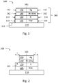
- Figure 1 shows an exemplary semiconductor device 100 comprising a semiconductor substrate 110, a TiW layer 120, a Ti layer 130, a Ni alloy layer 140, and an Ag layer 150.
- the Ni alloy layer 140 may comprise an alloy of nickel and another suitable element.
- NiV, NiSi and NiN are examples of suitable alloys, though it is contemplated that other nickel alloys might also be suitable.
- an embodiment utilizing a NiV layer will be described from this point forward.
- the TiW layer 120 is arranged on the semiconductor substrate 110, e.g. on a first main side 111.
- the Ti layer 130 is arranged on the TiW layer 120, in particular directly on the TiW layer 120.
- the NiV layer 140 is arranged on the Ti layer 130, in particular directly on the Ti layer 130.
- the Ag layer 150 is arranged on the NiV layer 140, in particular directly on the NiV layer 140.
- the TiW layer 120, the Ti layer 130, the NiV layer 140, and the Ag layer 150 comprise respective side faces 122, 132, 142, 152 which may be arranged at an angle with respect to the first main side 111 of the semiconductor substrate.
- one or more of the side faces 122, 132, 142, 152 may be arranged essentially perpendicular with respect to the first main side 111.
- the side faces 152 of the Ag layer 150 and the side faces 142 of the NiV layer 140 are fabricated by a wet etching process.
- the side faces 152, 142 comprise a surface structure and/or a microstructure that is fabricated by a wet etching process.
- the side faces 132 of the Ti layer 130 and the side faces 122 of the TiW layer 120 are fabricated by a dry etching process.
- the side faces 132, 122 comprise a surface structure and/or a microstructure that is fabricated by a dry etching process.
- the semiconductor substrate 110 may for example comprise a semiconductor wafer, a semiconductor panel, or a singulated semiconductor die.
- the semiconductor substrate 110 may have any suitable thickness measured perpendicular to the first main side 111.
- the semiconductor device 100 comprises a dielectric layer arranged between the semiconductor substrate 110 and the TiW layer 120.
- the dielectric layer may for example comprise or consist of a polymer, e.g. an imide.
- the TiW layer 120 may be arranged at least partially directly on the dielectric layer.
- the TiW layer 120 may comprise Ti and W or it may completely consist of Ti and W, except for unavoidable contaminants.
- the TiW layer 120 may comprise any suitable ratio of Ti to W.
- the Ti layer 130 may comprise or consist of Ti, except for unavoidable contaminants.
- the NiV layer 140 may comprise or consist of Ni and V in any suitable ratio and it may comprise unavoidable contaminants.
- the Ag layer 150 may comprise or consist of Ag and it may also comprise unavoidable contaminants.
- the layers 120, 130, 140, and 150 may have any suitable thickness measured perpendicular to the first main side 111.
- the TiW layer 120 has a thickness in the range of 100nm to 300nm, e.g. about 150nm.
- the Ti layer 130 may for example have a thickness in the range of 5nm to 150nm, e.g. about 100nm.
- the NiV layer 140 may for example have a thickness in the range of 100nm to 500nm, e.g. about 300nm.
- the Ag layer 150 may for example have a thickness in the range of 200nm to 800nm, e.g. about 450nm.
- the Ag layer 150 may be configured as a sinter layer, meaning that the semiconductor device 100 may be electrically and mechanically coupled to a substrate by sintering the Ag layer 150 to the substrate.
- the Ag layer 150 may essentially be comprised of an Ag film deposited on the NiV layer 140.
- the Ag layer 150 may comprise voids between individual Ag particles, wherein during sintering the semiconductor device 100 to a substrate, these voids shrink.
- all respective side faces 122, 132, 142, 152 are essentially coplanar (i.e. all side faces 122, 132, 142, 152 on the left side in Fig. 1 are essentially coplanar and all side faces 122, 132, 142, 152 on the right side in Fig. 1 are essentially coplanar).
- one or more of the side faces 122, 132, 142, 152 are not coplanar with the others.
- the side faces 122, 132 of the TiW layer 120 and the Ti layer 130 may be coplanar or almost coplanar with each other but not coplanar with the side faces 142, 152 of the NiV layer 140 and the Ag layer 150.
- the metal layers 120, 130, 140, and 150 may be part of a layer stack 160.
- the layer stack 160 may have a center line 161 which is arranged perpendicular to the first main side 111 and which is also arranged essentially at the middle of each of the layers 120, 130, 140, 150 or at least at the middle of the majority of the layers 120, 130, 140, 150.
- one or more of the side faces 122, 132, 142, 152 are recessed towards the center line 161 with respect to the other side faces.
- an upper one of the side faces 122, 132, 142, 152 (as seen from above the Ag layer 150) may be recessed with respect to a lower one of the side faces 122, 132, 142, 152.
- the side faces 142 of the NiV layer 140 may be recessed towards the center line 161 with respect to the side faces 132 of the Ti layer 130.
- the layer stack 160 is free of any undercut between the layers 120, 130, 140, and 150.
- no side face of a lower one of the layers 120, 130, 140, 150 is recessed towards the center line 161 with respect to a respective side face of an upper one of the layers 120, 130, 140, 150.
- the TiW layer 120 has at least the same lateral extension (measured perpendicular to the center line 161) from the center line 161 as the Ti layer 130; the Ti layer 130 has at least the same lateral extension from the center line 161 as the NiV layer 140; the NiV layer 140 has at least the same lateral extension from the center line 161 as the Ag layer 150.
- the TiW layer 120 and Ti layer 130 are patterned by dry etching, whereas the NiV layer 140 and the Ag layer 150 are patterned by wet etching.
- One advantage of this two-step etching scheme may be that different metal materials may exhibit different etching rates which may make it difficult or impossible to obtain a smooth side face profile (in particular a side face profile free of any undercuts) in only one single etching process.
- a wet etching process for patterning the upper layers (NiV layer 140 and Ag layer 150) and using a subsequent dry etching process for patterning the lower layers (TiW layer 120 and Ti layer 130) however an optimal side face profile free of any undercuts can be obtained.
- Figure 2 shows a semiconductor device 200 which may be similar to or identical with the semiconductor device 100.
- the NiV layer 140 and the Ag layer 150 are recessed towards the center line 161 with respect to the TiW layer 120 and the Ti layer 130.
- This offset between the NiV layer 140 and Ag layer 150 on the one hand and the TiW layer 120 and Ti layer 130 on the other hand may for example be due to the fact that two different etching processes were used to pattern the layers 140, 150 and 120, 130.
- the NiV layer 140 and Ag layer 150 may e.g. be patterned with a wet etching process and the TiW layer 120 and Ti layer 130 may be patterned with a dry etching process.
- the offset between the NiV layer 140 and Ag layer 150 on the one hand and the TiW layer 120 and Ti layer 130 on the other hand has a length 1 of 1 ⁇ m or more, or 2 ⁇ m or more, or 3 ⁇ m or more, or 4 ⁇ m or more, or 5 ⁇ m or more.
- the semiconductor device 200 comprises a further offset between the TiW layer 120 and the Ti layer and/or a further offset between the NiV layer 140 and the Ag layer 150.
- the further offsets may have a shorter length than the length 1 of the offset between the Ti layer 130 and the NiV layer 140 shown in Fig. 2 .
- the further offsets may have a length of 1 ⁇ m or less, or 500nm or less, or 100nm or less.
- an exposed part of an upper side 133 of the Ti layer 130 may have a microstructure essentially fabricated by a wet etching process.
- the exposed part of the upper side 133 is that part of the upper side 133 that is not covered by the NiV layer 140.
- the microstructure of the exposed part of the upper side 133 may be formed while wet etching the NiV layer 140 and Ag layer 150.
- Figure 3 shows a semiconductor device 300 which may be similar to or identical with the semiconductor devices 100 and 200.
- the side faces 142 of the NiV layer 140 are arranged at an angle ⁇ 1 with respect to the first main side 111, wherein the angle ⁇ 1 is smaller than 90°.
- the side faces 152 of the Ag layer 150 are arranged at an angle ⁇ 2 with respect to the first main side 111, wherein the angle ⁇ 2 is also smaller than 90°.
- the side faces 122, 132 of the TiW layer 120 and Ti layer 130 on the other hand may be arranged perpendicular or essentially perpendicular with respect to the first main side 111.
- the side faces 142, 152 of the NiV layer 140 and Ag layer 150 being sloped and the side faces 122, 132 of the TiW layer 120 and Ti layer 120 being vertical may be due to the different etching techniques used to pattern the layers 140, 150 and 120, 130.
- a wet etching process is an isotropic patterning process which may produce sloped side faces, whereas dry etching is an anisotropic patterning process which may produce vertical or almost vertical side faces.
- angles ⁇ 1 and ⁇ 2 need not necessarily be identical. However, it is also possible that they are identical or almost identical.
- the angles ⁇ 1 and ⁇ 2 may have any value, dependent on the specific etching parameters used, e.g. 80° or less, or 70° or less, or 60° or less, or 50° or less.
- the side faces 142 and 152 there is an offset between the side faces 142 and 152, e.g. a small offset of no more than 5 ⁇ m or no more than 1 ⁇ m, or no more than 500nm.
- the side faces 142 and 152 are essentially coplanar.
- the side faces 142, 152 need not necessarily be planar and may e.g. have a bent shape.
- Figures 4A to 4F show the semiconductor device 300 in various stages of fabrication, according to an exemplary method for fabricating semiconductor devices. A similar method may be used to fabricate the semiconductor devices 100 and 200.
- the semiconductor substrate 110 is provided. This may comprise arranging the semiconductor substrate 110 on a temporary carrier, e.g. a tape.
- a dielectric layer like an imide layer may be deposited on the first main side 111.
- the dielectric layer may be patterned in order to provide an electrical contact to e.g. transistor structures of the semiconductor substrate 110.
- the first main side 111 is a backside of the semiconductor substrate 110 and according to another example, it is a front side of the semiconductor substrate 110.
- the layer stack 160 is deposited on the first main side 111 of the semiconductor substrate 110.
- the individual layers 120, 130, 140, and 150 of the layer stack 160 may e.g. be deposited in individual, subsequent processes.
- One or more of the layers 120, 130, and 140 may e.g. be deposited using a sputtering process, an electroplating process, a vapor deposition process, or any other suitable deposition technique.
- the Ag layer 150 may e.g. be deposited using a spraying process, a cold plasma assisted deposition process, or any other suitable deposition technique.
- the layer stack 160 may be deposited such that it completely covers the first main side 111 of the semiconductor substrate 110 or it may be deposited such that it covers the first main side 111 only partially (e.g. by using an appropriate mask).
- a photoresist layer 410 is deposited on the Ag layer 150.
- the photoresist layer 410 may be applied such that it completely covers the Ag layer 150. Any suitable type of photoresist may be used, e.g. IX335.
- the photoresist layer 410 may be patterned using any suitable photolithography technique.
- a wet etching process is used to etch the Ag layer 150 and the NiV layer 140.
- the wet etching chemistry 420 may be chosen such that the Ag layer 150 and NiV layer 140 are readily etched, whereas the Ti layer 130 and TiW layer 120 are not readily etched.
- the wet etching chemistry 420 comprises a solution comprising phosphoric acid, acetic acid and nitric acid.
- One exemplary wet etching solution comprises 47.5% phosphoric acid, 1.5% nitric acid, 35% acetic acid and 16% water.
- the wet etching process may essentially be an isotropic patterning process. Therefore, the Ag layer 150 and/or NiV layer 140 may form an undercut under the photoresist layer 410.
- a dry etching process is used to etch the Ti layer 130 and TiW layer 120.
- Dry etching may e.g. be done with an etching gas 430 comprising chlorine and fluorine (e.g. Cl 2 and SF 6 ) .
- the dry etching process may e.g. comprise reactive ion etching or any other suitable technique.
- particles of the etching gas 430 may be accelerated towards the first main side 111, thereby anisotropically etching the Ti layer 130 and TiW layer 120. Since the Ag layer 150 and NiV layer 140 are covered by the photoresist layer 410, no dry etching is performed on these layers, according to an example.
- the same photoresist layer 410 may be used for both the wet etching process shown in Fig. 4E and the dry etching process shown in Fig. 4F . However, it is also possible that the photoresist 410 is removed after the wet etching process and new photoresist 410 is applied in a further photolithography process, prior to the dry etching process.
- the dry etching process is performed within 12 hours or less of the wet etching process, or within 6 hours or less, or within 1 hour or less.
- the dry etching process is stopped once the dielectric layer beneath the TiW layer 120 is reached.
- This may e.g. be determined by spectrographically checking for particles of the dielectric layer (e.g. imides in the case that the dielectric layer is an imide layer) are alternatively for particles of the semiconductor substrate 110 in the exhaust gas of the etching chamber.
- the etching apparatus may be equipped with a spectrometer for this purpose. The etching process may be stopped automatically once the particles of the dielectric layer or the semiconductor substrate 110 are detected by the spectrometer.
- the wet etching process as described with respect to Fig. 4E is used for etching the Ag layer 150, the NiV layer 140, and also the Ti layer 130.
- the dry etching process as described with respect to Fig. 4F is only used for etching the TiW layer 120. In this case, tight control of the etching times may be necessary in order to obtain satisfying etching results.
- the TiW layer 120 and Ti layer 130 are deposited on the semiconductor substrate 110 as described with respect to Fig. 4B . Consequently, photoresist 410 is deposited on the Ti layer 130, a lithography process is performed and the TiW layer 120 and Ti layer 130 are dry etched.
- the Ti layer 130 may be striped, e.g. by using hydrofluoric acid, in order to preserve a clean TiW surface (avoid contact of TiW with photoresist).
- a new Ti layer 130, the NiV layer 140 and the Ag layer 150 may be deposited and patterned by wet etching.
- Figure 5 is a flow chart of an exemplary method 500 for fabricating a semiconductor device.
- the method 500 may for example be used for fabricating the semiconductor devices 100, 200 and 300.
- the method 500 comprises at 501 an act of depositing a TiW layer on a semiconductor substrate, at 502 an act of depositing a Ti layer on the TiW layer, at 503 an act of depositing a Ni alloy layer on the Ti layer, at 504 an act of depositing an Ag layer on the Ni alloy layer, at 505 an act of at least partially covering the Ag layer with photoresist, at 506 an act of wet etching the Ag layer and the Ni alloy layer, and at 507 an act of dry etching the Ti layer and the TiW layer.
- the wet etching at 506 may for example be done using a solution comprising phosphoric acid, acetic acid and nitric acid.
- the dry etching at 507 may for example be done using an etching gas comprising chlorine and fluorine.
Landscapes
- Chemical & Material Sciences (AREA)
- Chemical Kinetics & Catalysis (AREA)
- General Chemical & Material Sciences (AREA)
- Engineering & Computer Science (AREA)
- Materials Engineering (AREA)
- Mechanical Engineering (AREA)
- Metallurgy (AREA)
- Organic Chemistry (AREA)
- Electrodes Of Semiconductors (AREA)
Abstract
Description
- This disclosure relates in general to a method for fabricating semiconductor devices, wherein wet etching and dry etching are used, as well as to a semiconductor device.
- Semiconductor devices, in particular power semiconductor devices, may comprise electrical interconnections which need to be able to carry a large electrical current and/or withstand a high voltage. This requirement for example affects an interconnection between a load electrode of a power semiconductor die and a substrate like e.g. a leadframe, a direct copper bond (DCB), a direct aluminum bond (DAB), an active metal brazing (AMB), etc. One possible interconnection technique comprises sintering the semiconductor die to the substrate using a dedicated sintering metal layer. The specific material for the sintering metal layer may for example be chosen based on its high electrical and thermal conductivity, low processing temperature, high reliability, low cost, etc. Manufacturing of such an interconnection comprising a sintering metal layer may comprise depositing a stack of different metals on the semiconductor substrate beneath the sintering metal layer. The metal layers of this stack may for example be configured as diffusion barrier layer, inter-adhesion layer, etc. Furthermore, the metal stack may need to be patterned in order to define metallization areas on the chip. This patterning process should not be too time consuming in order to save costs, but it should also produce clean sidewall profiles and avoid undercuts in the patterned metal stack which otherwise could pose reliability risks due to their potential for trapping humidity. Improved methods for fabricating semiconductor devices as well as improved semiconductor devices may help with solving these and other problems.
- The problem on which the invention is based is solved by the features of the independent claims. Further advantageous examples are described in the dependent claims.
- Various aspects pertain to a method for fabricating a semiconductor device, the method comprising: depositing a TiW layer on a semiconductor substrate, depositing a Ti layer on the TiW layer, depositing a Ni alloy layer on the Ti layer, depositing an Ag layer on the Ni alloy layer, at least partially covering the Ag layer with photoresist, wet etching the Ag layer and the Ni alloy layer, and dry etching the Ti layer and the TiW layer.
- Various aspects pertain to a semiconductor device, comprising: a semiconductor substrate, a TiW layer arranged on the semiconductor substrate, a Ti layer arranged on the TiW layer, a Ni alloy layer arranged on the Ti layer, and an Ag layer arranged on the Ni alloy layer, wherein the Ag layer and the Ni alloy layer comprise side faces fabricated by at least one wet etching process, and wherein the Ti layer and the TiW layer comprise side faces fabricated by a dry etching process.
- The accompanying drawings illustrate examples and together with the description serve to explain principles of the disclosure. Other examples and many of the intended advantages of the disclosure will be readily appreciated as they become better understood by reference to the following detailed description. The elements of the drawings are not necessarily to scale relative to each other. Identical reference numerals designate corresponding similar parts.
-
Figure 1 shows a sectional view of a semiconductor device comprising a metal layer stack, wherein first ones of the metal layers are patterned by wet etching and second ones of the metal layers are patterned by dry etching. -
Figure 2 shows a sectional view of a further semiconductor device, wherein upper metal layers of a metal layer stack are recessed with respect to lower metal layers of the metal layer stack. -
Figure 3 shows a sectional view of a further semiconductor device, wherein side walls of first metal layers of a metal layer stack are arranged at an angle of less than 90° with respect to a first main side of a semiconductor substrate, and wherein side walls of second metal layers of a metal layer stack are perpendicular to the first main side. -
Figures 4A to 4F show a semiconductor device in various stages of fabrication, according to an exemplary method for fabricating semiconductor devices. -
Figure 5 is a flow chart of an exemplary method for fabricating semiconductor devices. - In the following detailed description, directional terminology, such as "top", "bottom", "left", "right", "upper", "lower" etc., is used with reference to the orientation of the Figure(s) being described. Because components of the disclosure can be positioned in a number of different orientations, the directional terminology is used for purposes of illustration only.
- In addition, while a particular feature or aspect of an example may be disclosed with respect to only one of several implementations, such feature or aspect may be combined with one or more other features or aspects of the other implementations as may be desired and advantageous for any given or particular application, unless specifically noted otherwise or unless technically restricted. Also, the term "exemplary" is merely meant as an example, rather than the best or optimal.
- The examples of a semiconductor device may comprise various types of semiconductor chips or circuits incorporated in the semiconductor chips, among them AC/DC or DC/DC converter circuits, power MOS transistors, power Schottky diodes, JFETs (Junction Gate Field Effect Transistors), power bipolar transistors, logic integrated circuits, analogue integrated circuits, power integrated circuits, chips with integrated passives, etc.
- The semiconductor chip(s) can be manufactured from specific semiconductor material, for example Si, SiC, SiGe, GaAs, GaN, or from any other semiconductor material, and, furthermore, may contain one or more of inorganic and organic materials that are not semiconductors, such as for example insulators, plastics or metals.
- The semiconductor chips may have contact pads (or electrodes) which allow electrical contact to be made with the integrated circuits included in the semiconductor chips. The electrodes may be arranged all at only one main face of the semiconductor chips or at both main faces of the semiconductor chips. They may include one or more electrode metal layers which are applied to the semiconductor material of the semiconductor chips. The electrode metal layers may be manufactured with any desired geometric shape and any desired material composition.
- The notation XY refers to an alloy of X including at least Y as a further component. In particular, it may refer to an alloy of X including Y as a sole residual component (i.e. a closed composition). That is, in the second case, the notation XY means that the alloy XY has a composition consisting of X (of the percentage in weight of X) and Y (of the percentage in weight of Y), the balance being only inevitable elements. The notation XYZ... has an analogous meaning, i.e. an "open composition" or a "closed composition" with X, Y, Z ... forming the sole constituents of the alloy (except inevitable elements).
-
Figure 1 shows anexemplary semiconductor device 100 comprising asemiconductor substrate 110, aTiW layer 120, aTi layer 130, aNi alloy layer 140, and anAg layer 150. - The Ni
alloy layer 140 may comprise an alloy of nickel and another suitable element. NiV, NiSi and NiN are examples of suitable alloys, though it is contemplated that other nickel alloys might also be suitable. For simplicity, an embodiment utilizing a NiV layer will be described from this point forward. - The
TiW layer 120 is arranged on thesemiconductor substrate 110, e.g. on a firstmain side 111. TheTi layer 130 is arranged on theTiW layer 120, in particular directly on theTiW layer 120. TheNiV layer 140 is arranged on theTi layer 130, in particular directly on theTi layer 130. TheAg layer 150 is arranged on theNiV layer 140, in particular directly on theNiV layer 140. - The
TiW layer 120, theTi layer 130, theNiV layer 140, and theAg layer 150 compriserespective side faces main side 111 of the semiconductor substrate. For example, one or more of the side faces 122, 132, 142, 152 may be arranged essentially perpendicular with respect to the firstmain side 111. - The side faces 152 of the
Ag layer 150 and the side faces 142 of theNiV layer 140 are fabricated by a wet etching process. In other words, the side faces 152, 142 comprise a surface structure and/or a microstructure that is fabricated by a wet etching process. The side faces 132 of theTi layer 130 and the side faces 122 of theTiW layer 120 are fabricated by a dry etching process. In other words, the side faces 132, 122 comprise a surface structure and/or a microstructure that is fabricated by a dry etching process. - The
semiconductor substrate 110 may for example comprise a semiconductor wafer, a semiconductor panel, or a singulated semiconductor die. Thesemiconductor substrate 110 may have any suitable thickness measured perpendicular to the firstmain side 111. - According to an example, the
semiconductor device 100 comprises a dielectric layer arranged between thesemiconductor substrate 110 and theTiW layer 120. The dielectric layer may for example comprise or consist of a polymer, e.g. an imide. TheTiW layer 120 may be arranged at least partially directly on the dielectric layer. - The
TiW layer 120 may comprise Ti and W or it may completely consist of Ti and W, except for unavoidable contaminants. TheTiW layer 120 may comprise any suitable ratio of Ti to W. Likewise, theTi layer 130 may comprise or consist of Ti, except for unavoidable contaminants. TheNiV layer 140 may comprise or consist of Ni and V in any suitable ratio and it may comprise unavoidable contaminants. TheAg layer 150 may comprise or consist of Ag and it may also comprise unavoidable contaminants. - The
layers main side 111. According to an example, theTiW layer 120 has a thickness in the range of 100nm to 300nm, e.g. about 150nm. TheTi layer 130 may for example have a thickness in the range of 5nm to 150nm, e.g. about 100nm. TheNiV layer 140 may for example have a thickness in the range of 100nm to 500nm, e.g. about 300nm. TheAg layer 150 may for example have a thickness in the range of 200nm to 800nm, e.g. about 450nm. - The
Ag layer 150 may be configured as a sinter layer, meaning that thesemiconductor device 100 may be electrically and mechanically coupled to a substrate by sintering theAg layer 150 to the substrate. TheAg layer 150 may essentially be comprised of an Ag film deposited on theNiV layer 140. TheAg layer 150 may comprise voids between individual Ag particles, wherein during sintering thesemiconductor device 100 to a substrate, these voids shrink. - According to an example, all respective side faces 122, 132, 142, 152 are essentially coplanar (i.e. all side faces 122, 132, 142, 152 on the left side in
Fig. 1 are essentially coplanar and all side faces 122, 132, 142, 152 on the right side inFig. 1 are essentially coplanar). According to another example, one or more of the side faces 122, 132, 142, 152 are not coplanar with the others. For example, the side faces 122, 132 of theTiW layer 120 and theTi layer 130 may be coplanar or almost coplanar with each other but not coplanar with the side faces 142, 152 of theNiV layer 140 and theAg layer 150. - The metal layers 120, 130, 140, and 150 may be part of a
layer stack 160. Thelayer stack 160 may have acenter line 161 which is arranged perpendicular to the firstmain side 111 and which is also arranged essentially at the middle of each of thelayers layers - According to an example, one or more of the side faces 122, 132, 142, 152 are recessed towards the
center line 161 with respect to the other side faces. In particular, an upper one of the side faces 122, 132, 142, 152 (as seen from above the Ag layer 150) may be recessed with respect to a lower one of the side faces 122, 132, 142, 152. For example, the side faces 142 of theNiV layer 140 may be recessed towards thecenter line 161 with respect to the side faces 132 of theTi layer 130. - According to an example, the
layer stack 160 is free of any undercut between thelayers layers center line 161 with respect to a respective side face of an upper one of thelayers TiW layer 120 has at least the same lateral extension (measured perpendicular to the center line 161) from thecenter line 161 as theTi layer 130; theTi layer 130 has at least the same lateral extension from thecenter line 161 as theNiV layer 140; theNiV layer 140 has at least the same lateral extension from thecenter line 161 as theAg layer 150. - As mentioned above, the
TiW layer 120 andTi layer 130 are patterned by dry etching, whereas theNiV layer 140 and theAg layer 150 are patterned by wet etching. One advantage of this two-step etching scheme may be that different metal materials may exhibit different etching rates which may make it difficult or impossible to obtain a smooth side face profile (in particular a side face profile free of any undercuts) in only one single etching process. By using a wet etching process for patterning the upper layers (NiV layer 140 and Ag layer 150) and using a subsequent dry etching process for patterning the lower layers (TiW layer 120 and Ti layer 130) however an optimal side face profile free of any undercuts can be obtained. -
Figure 2 shows asemiconductor device 200 which may be similar to or identical with thesemiconductor device 100. In thesemiconductor device 200, theNiV layer 140 and theAg layer 150 are recessed towards thecenter line 161 with respect to theTiW layer 120 and theTi layer 130. This offset between theNiV layer 140 andAg layer 150 on the one hand and theTiW layer 120 andTi layer 130 on the other hand may for example be due to the fact that two different etching processes were used to pattern thelayers NiV layer 140 andAg layer 150 may e.g. be patterned with a wet etching process and theTiW layer 120 andTi layer 130 may be patterned with a dry etching process. - According to an example, the offset between the
NiV layer 140 andAg layer 150 on the one hand and theTiW layer 120 andTi layer 130 on the other hand has a length 1 of 1µm or more, or 2µm or more, or 3µm or more, or 4µm or more, or 5µm or more. - According to an example, the
semiconductor device 200 comprises a further offset between theTiW layer 120 and the Ti layer and/or a further offset between theNiV layer 140 and theAg layer 150. The further offsets may have a shorter length than the length 1 of the offset between theTi layer 130 and theNiV layer 140 shown inFig. 2 . For example, the further offsets may have a length of 1µm or less, or 500nm or less, or 100nm or less. - According to an example, an exposed part of an
upper side 133 of theTi layer 130 may have a microstructure essentially fabricated by a wet etching process. The exposed part of theupper side 133 is that part of theupper side 133 that is not covered by theNiV layer 140. The microstructure of the exposed part of theupper side 133 may be formed while wet etching theNiV layer 140 andAg layer 150. -
Figure 3 shows asemiconductor device 300 which may be similar to or identical with thesemiconductor devices semiconductor device 300, the side faces 142 of theNiV layer 140 are arranged at an angle α1 with respect to the firstmain side 111, wherein the angle α1 is smaller than 90°. Furthermore, the side faces 152 of theAg layer 150 are arranged at an angle α2 with respect to the firstmain side 111, wherein the angle α2 is also smaller than 90°. The side faces 122, 132 of theTiW layer 120 andTi layer 130 on the other hand may be arranged perpendicular or essentially perpendicular with respect to the firstmain side 111. - The side faces 142, 152 of the
NiV layer 140 andAg layer 150 being sloped and the side faces 122, 132 of theTiW layer 120 andTi layer 120 being vertical may be due to the different etching techniques used to pattern thelayers - The angles α1 and α2 need not necessarily be identical. However, it is also possible that they are identical or almost identical. The angles α1 and α2 may have any value, dependent on the specific etching parameters used, e.g. 80° or less, or 70° or less, or 60° or less, or 50° or less.
- According to an example, there is an offset between the side faces 142 and 152, e.g. a small offset of no more than 5µm or no more than 1µm, or no more than 500nm. However, it is also possible that the side faces 142 and 152 are essentially coplanar. Furthermore, the side faces 142, 152 need not necessarily be planar and may e.g. have a bent shape.
-
Figures 4A to 4F show thesemiconductor device 300 in various stages of fabrication, according to an exemplary method for fabricating semiconductor devices. A similar method may be used to fabricate thesemiconductor devices - As shown in
Figure 4A , thesemiconductor substrate 110 is provided. This may comprise arranging thesemiconductor substrate 110 on a temporary carrier, e.g. a tape. According to an example, a dielectric layer like an imide layer (not shown inFig. 4A ) may be deposited on the firstmain side 111. The dielectric layer may be patterned in order to provide an electrical contact to e.g. transistor structures of thesemiconductor substrate 110. According to an example, the firstmain side 111 is a backside of thesemiconductor substrate 110 and according to another example, it is a front side of thesemiconductor substrate 110. - As shown in
Figure 4B , thelayer stack 160 is deposited on the firstmain side 111 of thesemiconductor substrate 110. Theindividual layers layer stack 160 may e.g. be deposited in individual, subsequent processes. - One or more of the
layers Ag layer 150 may e.g. be deposited using a spraying process, a cold plasma assisted deposition process, or any other suitable deposition technique. - The
layer stack 160 may be deposited such that it completely covers the firstmain side 111 of thesemiconductor substrate 110 or it may be deposited such that it covers the firstmain side 111 only partially (e.g. by using an appropriate mask). - As shown in
Figure 4C , aphotoresist layer 410 is deposited on theAg layer 150. Thephotoresist layer 410 may be applied such that it completely covers theAg layer 150. Any suitable type of photoresist may be used, e.g. IX335. - As shown in
Figure 4D , thephotoresist layer 410 may be patterned using any suitable photolithography technique. - As shown in
Figure 4E , a wet etching process is used to etch theAg layer 150 and theNiV layer 140. Thewet etching chemistry 420 may be chosen such that theAg layer 150 andNiV layer 140 are readily etched, whereas theTi layer 130 andTiW layer 120 are not readily etched. According to an example, thewet etching chemistry 420 comprises a solution comprising phosphoric acid, acetic acid and nitric acid. One exemplary wet etching solution comprises 47.5% phosphoric acid, 1.5% nitric acid, 35% acetic acid and 16% water. - The wet etching process may essentially be an isotropic patterning process. Therefore, the
Ag layer 150 and/orNiV layer 140 may form an undercut under thephotoresist layer 410. - As shown in
Figure 4F , a dry etching process is used to etch theTi layer 130 andTiW layer 120. Dry etching may e.g. be done with anetching gas 430 comprising chlorine and fluorine (e.g. Cl2 and SF6) . The dry etching process may e.g. comprise reactive ion etching or any other suitable technique. In particular, particles of theetching gas 430 may be accelerated towards the firstmain side 111, thereby anisotropically etching theTi layer 130 andTiW layer 120. Since theAg layer 150 andNiV layer 140 are covered by thephotoresist layer 410, no dry etching is performed on these layers, according to an example. - The
same photoresist layer 410 may be used for both the wet etching process shown inFig. 4E and the dry etching process shown inFig. 4F . However, it is also possible that thephotoresist 410 is removed after the wet etching process andnew photoresist 410 is applied in a further photolithography process, prior to the dry etching process. - According to an example, the dry etching process is performed within 12 hours or less of the wet etching process, or within 6 hours or less, or within 1 hour or less.
- According to an example, the dry etching process is stopped once the dielectric layer beneath the
TiW layer 120 is reached. This may e.g. be determined by spectrographically checking for particles of the dielectric layer (e.g. imides in the case that the dielectric layer is an imide layer) are alternatively for particles of thesemiconductor substrate 110 in the exhaust gas of the etching chamber. The etching apparatus may be equipped with a spectrometer for this purpose. The etching process may be stopped automatically once the particles of the dielectric layer or thesemiconductor substrate 110 are detected by the spectrometer. - According to a further method for fabricating a semiconductor device, the wet etching process as described with respect to
Fig. 4E is used for etching theAg layer 150, theNiV layer 140, and also theTi layer 130. The dry etching process as described with respect toFig. 4F is only used for etching theTiW layer 120. In this case, tight control of the etching times may be necessary in order to obtain satisfying etching results. - According to yet another method for fabricating a semiconductor device, the
TiW layer 120 andTi layer 130 are deposited on thesemiconductor substrate 110 as described with respect toFig. 4B . Consequently,photoresist 410 is deposited on theTi layer 130, a lithography process is performed and theTiW layer 120 andTi layer 130 are dry etched. TheTi layer 130 may be striped, e.g. by using hydrofluoric acid, in order to preserve a clean TiW surface (avoid contact of TiW with photoresist). Afterwards, anew Ti layer 130, theNiV layer 140 and theAg layer 150 may be deposited and patterned by wet etching. -
Figure 5 is a flow chart of anexemplary method 500 for fabricating a semiconductor device. Themethod 500 may for example be used for fabricating thesemiconductor devices - The
method 500 comprises at 501 an act of depositing a TiW layer on a semiconductor substrate, at 502 an act of depositing a Ti layer on the TiW layer, at 503 an act of depositing a Ni alloy layer on the Ti layer, at 504 an act of depositing an Ag layer on the Ni alloy layer, at 505 an act of at least partially covering the Ag layer with photoresist, at 506 an act of wet etching the Ag layer and the Ni alloy layer, and at 507 an act of dry etching the Ti layer and the TiW layer. - The wet etching at 506 may for example be done using a solution comprising phosphoric acid, acetic acid and nitric acid. The dry etching at 507 may for example be done using an etching gas comprising chlorine and fluorine.
- In the following, the semiconductor device and the method for fabricating a semiconductor device are further described using specific examples.
- Example 1 is a method for fabricating a semiconductor device, the method comprising: depositing a TiW layer on a semiconductor substrate, depositing a Ti layer on the TiW layer, depositing a Ni alloy layer on the Ti layer, depositing an Ag layer on the Ni alloy layer, at least partially covering the Ag layer with photoresist, wet etching the Ag layer and the Ni alloy layer, and dry etching the Ti layer and the TiW layer.
- Example 2 is the method of example 1, wherein the wet etching is done using a solution comprising phosphoric, acetic and nitric acid.
- Example 3 is the method of example 1 or 2, wherein the dry etching is done using a gas comprising chlorine and fluorine.
- Example 4 is the method of one of the preceding examples, wherein the Ag layer, the Ni alloy layer, the Ti layer and the TiW layer form a layer stack, and wherein as viewed from above the Ag layer, after the dry etching each respective lower layer of the layer stack has a greater lateral extension than a respective upper layer of the layer stack, such that the layer stack is free of any undercuts between different layers of the layer stack.
- Example 5 is the method of one of the preceding examples, further comprising: during the dry etching, spectroscopically analyzing an exhaust gas for residues removed by the dry etching, and stopping the dry etching once residues of the semiconductor substrate or of a further layer arranged between the semiconductor substrate and the TiW layer are detected in the exhaust gas.
- Example 6 is the method of one of the preceding examples, wherein the dry etching is performed within no more than 12 hours of the wet etching, in particular within no more than 6 hours, further in particular within no more than 1 hour.
- Example 7 is the method of one of the preceding examples, wherein the photoresist is applied only once and is used for both the wet etching and the dry etching.
- Example 8 is the method of one of examples 1 to 6, wherein between the wet etching and the dry etching the photoresist is removed and then re-applied.
- Example 9 is the method of one of the preceding examples, further comprising: arranging an imide layer between the semiconductor substrate and the TiW layer.
- Example 10 is the method of one of the preceding examples, wherein the Ni alloy is selected from the group comprising NiV, NiSi and NiN.
- Example 11 is a semiconductor device, comprising: a semiconductor substrate, a TiW layer arranged on the semiconductor substrate, a Ti layer arranged on the TiW layer, a Ni alloy layer arranged on the Ti layer, and an Ag layer arranged on the Ni alloy layer, wherein the Ag layer and the Ni alloy layer comprise side faces fabricated by at least one wet etching process, and wherein the Ti layer and the TiW layer comprise side faces fabricated by a dry etching process.
- Example 12 is the semiconductor device of example 11, further comprising: an imide layer arranged between the semiconductor substrate and the TiW layer.
- Example 13 is the semiconductor device of example 11 or 12, wherein the TiW layer has a thickness in the range of 100nm to 300nm, measured perpendicular to a first main face of the semiconductor substrate, wherein the TiW layer is arranged on the first main face.
- Example 14 is the semiconductor device of one of examples 11 to 13, wherein the Ti layer has a thickness in the range of 5nm to 150nm, measured perpendicular to a first main face of the semiconductor substrate, wherein the TiW layer is arranged on the first main face.
- Example 15 is the semiconductor device of one of examples 11 to 14, wherein the Ni alloy layer has a thickness in the range of 100nm to 500nm, measured perpendicular to a first main face of the semiconductor substrate, wherein the TiW layer is arranged on the first main face.
- Example 16 is the semiconductor device of one of examples 11 to 15, wherein the Ag layer has a thickness in the range of 200nm to 800nm, measured perpendicular to a first main face of the semiconductor substrate, wherein the TiW layer is arranged on the first main face.
- Example 17 is an apparatus comprising means for performing the method of one of examples 1 to 10.
- While the disclosure has been illustrated and described with respect to one or more implementations, alterations and/or modifications may be made to the illustrated examples without departing from the spirit and scope of the appended claims. In particular regard to the various functions performed by the above described components or structures (assemblies, devices, circuits, systems, etc.), the terms (including a reference to a "means") used to describe such components are intended to correspond, unless otherwise indicated, to any component or structure which performs the specified function of the described component (e.g., that is functionally equivalent), even though not structurally equivalent to the disclosed structure which performs the function in the herein illustrated exemplary implementations of the disclosure.
Claims (16)
- A method for fabricating a semiconductor device, the method comprising:depositing a TiW layer on a semiconductor substrate,depositing a Ti layer on the TiW layer,depositing a Ni alloy layer on the Ti layer,depositing an Ag layer on the Ni alloy layer,at least partially covering the Ag layer with photoresist,wet etching the Ag layer and the Ni alloy layer, anddry etching the Ti layer and the TiW layer.
- The method of claim 1, wherein the wet etching is done using a solution comprising phosphoric acid, acetic acid and nitric acid.
- The method of claim 1 or 2, wherein the dry etching is done using a gas comprising chlorine and fluorine.
- The method of one of the preceding claims, wherein the Ag layer, the Ni alloy layer, the Ti layer and the TiW layer form a layer stack, and
wherein as viewed from above the Ag layer, after the dry etching each respective lower layer of the layer stack has a greater lateral extension than a respective upper layer of the layer stack, such that the layer stack is free of any undercuts between different layers of the layer stack. - The method of one of the preceding claims, further comprising:during the dry etching, spectroscopically analyzing an exhaust gas for residues removed by the dry etching, andstopping the dry etching once residues of the semiconductor substrate or of a further layer arranged between the semiconductor substrate and the TiW layer are detected in the exhaust gas.
- The method of one of the preceding claims, wherein the dry etching is performed within no more than 12 hours of the wet etching, in particular within no more than 6 hours, further in particular within no more than 1 hour.
- The method of one of the preceding claims, wherein the photoresist is applied only once and is used for both the wet etching and the dry etching.
- The method of one of claims 1 to 6, wherein between the wet etching and the dry etching, the photoresist is removed and then re-applied.
- The method of one of the preceding claims, further comprising:
arranging an imide layer between the semiconductor substrate and the TiW layer. - The method of one of the preceding claims, wherein the Ni alloy is selected from the group comprising NiV, NiSi and NiN.
- A semiconductor device, comprising:a semiconductor substrate,a TiW layer arranged on the semiconductor substrate,a Ti layer arranged on the TiW layer,a Ni alloy layer arranged on the Ti layer, andan Ag layer arranged on the Ni alloy layer,wherein the Ag layer and the Ni alloy layer comprise side faces fabricated by at least one wet etching process, andwherein the Ti layer and the TiW layer comprise side faces fabricated by a dry etching process.
- The semiconductor device of claim 11, further comprising:
an imide layer arranged between the semiconductor substrate and the TiW layer. - The semiconductor device of claim 11 or 12, wherein the TiW layer has a thickness in the range of 100nm to 300nm, measured perpendicular to a first main face of the semiconductor substrate, wherein the TiW layer is arranged on the first main face.
- The semiconductor device of one of claims 11 to 13, wherein the Ti layer has a thickness in the range of 5nm to 150nm, measured perpendicular to a first main face of the semiconductor substrate, wherein the TiW layer is arranged on the first main face.
- The semiconductor device of one of claims 11 to 14, wherein the Ni alloy layer has a thickness in the range of 100nm to 500nm, measured perpendicular to a first main face of the semiconductor substrate, wherein the TiW layer is arranged on the first main face.
- The semiconductor device of one of claims 11 to 15, wherein the Ag layer has a thickness in the range of 200nm to 800nm, measured perpendicular to a first main face of the semiconductor substrate, wherein the TiW layer is arranged on the first main face.
Priority Applications (4)
| Application Number | Priority Date | Filing Date | Title |
|---|---|---|---|
| EP21153306.2A EP4033518B1 (en) | 2021-01-25 | 2021-01-25 | Method for fabricating a semiconductor device using wet etching and dry etching and semiconductor device |
| CN202210077968.9A CN114792627A (en) | 2021-01-25 | 2022-01-24 | Method for manufacturing semiconductor device using wet etching and dry etching, and semiconductor device |
| US17/582,656 US12018387B2 (en) | 2021-01-25 | 2022-01-24 | Method for fabricating a semiconductor device using wet etching and dry etching and semiconductor device |
| US18/731,567 US12525555B2 (en) | 2021-01-25 | 2024-06-03 | Method for fabricating a semiconductor device using wet etching and dry etching and semiconductor device |
Applications Claiming Priority (1)
| Application Number | Priority Date | Filing Date | Title |
|---|---|---|---|
| EP21153306.2A EP4033518B1 (en) | 2021-01-25 | 2021-01-25 | Method for fabricating a semiconductor device using wet etching and dry etching and semiconductor device |
Publications (2)
| Publication Number | Publication Date |
|---|---|
| EP4033518A1 true EP4033518A1 (en) | 2022-07-27 |
| EP4033518B1 EP4033518B1 (en) | 2024-11-06 |
Family
ID=74346793
Family Applications (1)
| Application Number | Title | Priority Date | Filing Date |
|---|---|---|---|
| EP21153306.2A Active EP4033518B1 (en) | 2021-01-25 | 2021-01-25 | Method for fabricating a semiconductor device using wet etching and dry etching and semiconductor device |
Country Status (3)
| Country | Link |
|---|---|
| US (2) | US12018387B2 (en) |
| EP (1) | EP4033518B1 (en) |
| CN (1) | CN114792627A (en) |
Families Citing this family (3)
| Publication number | Priority date | Publication date | Assignee | Title |
|---|---|---|---|---|
| EP4057340A1 (en) * | 2021-03-08 | 2022-09-14 | Infineon Technologies Austria AG | Semiconductor device with a layer stack comprising a nisi layer and a niv layer for mounting on an electrically conductive layer, method for producing the same and corresponding mounted semiconductor arrangement |
| US20250006506A1 (en) * | 2023-06-27 | 2025-01-02 | Stmicroelectronics International N.V. | Single-mask stack etching methods for forming staircase structures |
| CN117637470B (en) * | 2023-11-30 | 2024-08-02 | 山东大学 | Etching method of double-layer metal of silicon carbide device |
Citations (4)
| Publication number | Priority date | Publication date | Assignee | Title |
|---|---|---|---|---|
| US20030082913A1 (en) * | 2001-10-26 | 2003-05-01 | Intel Corporation | Etchant formulation for selectively removing thin films in the presence of copper, tin, and lead |
| US20040113273A1 (en) * | 2002-09-10 | 2004-06-17 | William Tze-You Chen | Under-bump-metallurgy layer for improving adhesion |
| US20120074572A1 (en) * | 2010-09-28 | 2012-03-29 | Thomas Fischer | Semiconductor structure and method for making same |
| CN112259466A (en) * | 2019-07-22 | 2021-01-22 | 中芯长电半导体(江阴)有限公司 | Preparation method of rewiring layer |
Family Cites Families (11)
| Publication number | Priority date | Publication date | Assignee | Title |
|---|---|---|---|---|
| US5792672A (en) * | 1996-03-20 | 1998-08-11 | Chartered Semiconductor Manufacturing Ltd. | Photoresist strip method |
| US6210846B1 (en) * | 1999-08-13 | 2001-04-03 | Advanced Micro Devices, Inc. | Exposure during rework for enhanced resist removal |
| CN110004429B (en) * | 2012-03-27 | 2021-08-31 | 诺发系统公司 | Tungsten Feature Fill |
| JP2014060341A (en) | 2012-09-19 | 2014-04-03 | Toshiba Corp | Semiconductor device and semiconductor device manufacturing method |
| US9006899B2 (en) | 2012-12-14 | 2015-04-14 | Infineon Technologies Ag | Layer stack |
| US9093385B2 (en) * | 2013-05-28 | 2015-07-28 | Infineon Technologies Ag | Method for processing a semiconductor workpiece with metallization |
| US9627335B2 (en) * | 2014-05-08 | 2017-04-18 | Infineon Technologies Ag | Method for processing a semiconductor workpiece and semiconductor workpiece |
| US9564409B2 (en) | 2015-01-27 | 2017-02-07 | Semiconductor Components Industries, Llc | Methods of forming semiconductor packages with an intermetallic layer comprising tin and at least one of silver, copper or nickel |
| US9786620B2 (en) * | 2015-07-27 | 2017-10-10 | Infineon Technolgies Ag | Semiconductor device and a method for manufacturing a semiconductor device |
| US9640497B1 (en) | 2016-06-30 | 2017-05-02 | Semiconductor Components Industries, Llc | Semiconductor backmetal (BM) and over pad metallization (OPM) structures and related methods |
| CN107579032B (en) | 2017-07-27 | 2019-04-09 | 厦门市三安集成电路有限公司 | A backside process method for compound semiconductor devices |
-
2021
- 2021-01-25 EP EP21153306.2A patent/EP4033518B1/en active Active
-
2022
- 2022-01-24 CN CN202210077968.9A patent/CN114792627A/en active Pending
- 2022-01-24 US US17/582,656 patent/US12018387B2/en active Active
-
2024
- 2024-06-03 US US18/731,567 patent/US12525555B2/en active Active
Patent Citations (4)
| Publication number | Priority date | Publication date | Assignee | Title |
|---|---|---|---|---|
| US20030082913A1 (en) * | 2001-10-26 | 2003-05-01 | Intel Corporation | Etchant formulation for selectively removing thin films in the presence of copper, tin, and lead |
| US20040113273A1 (en) * | 2002-09-10 | 2004-06-17 | William Tze-You Chen | Under-bump-metallurgy layer for improving adhesion |
| US20120074572A1 (en) * | 2010-09-28 | 2012-03-29 | Thomas Fischer | Semiconductor structure and method for making same |
| CN112259466A (en) * | 2019-07-22 | 2021-01-22 | 中芯长电半导体(江阴)有限公司 | Preparation method of rewiring layer |
Also Published As
| Publication number | Publication date |
|---|---|
| US12018387B2 (en) | 2024-06-25 |
| US20240318320A1 (en) | 2024-09-26 |
| EP4033518B1 (en) | 2024-11-06 |
| US20220235470A1 (en) | 2022-07-28 |
| CN114792627A (en) | 2022-07-26 |
| US12525555B2 (en) | 2026-01-13 |
Similar Documents
| Publication | Publication Date | Title |
|---|---|---|
| US12525555B2 (en) | Method for fabricating a semiconductor device using wet etching and dry etching and semiconductor device | |
| US7897484B2 (en) | Fabricating a top conductive layer in a semiconductor die | |
| US7947592B2 (en) | Thick metal interconnect with metal pad caps at selective sites and process for making the same | |
| US10573611B2 (en) | Solder metallization stack and methods of formation thereof | |
| US9633957B2 (en) | Semiconductor device, a power semiconductor device, and a method for processing a semiconductor device | |
| US20140035167A1 (en) | Method for producing a bonding pad for thermocompression bonding, and bonding pad | |
| US8264072B2 (en) | Electronic device | |
| US10651140B2 (en) | Semiconductor device with metal structure electrically connected to a conductive structure | |
| US8946902B2 (en) | Device and method for manufacturing a device | |
| US9911686B2 (en) | Source down semiconductor devices and methods of formation thereof | |
| CN206639796U (en) | Semiconductor devices | |
| US10276502B2 (en) | Semiconductor device and method for manufacturing same | |
| US9006899B2 (en) | Layer stack | |
| US11984321B1 (en) | Method for etching deep, high-aspect ratio features into silicon carbide and gallium nitride | |
| US7955969B2 (en) | Ultra thin FET | |
| CN105934813B (en) | semiconductor device | |
| US20170053879A1 (en) | Method, a semiconductor device and a layer arrangement | |
| US20170154974A1 (en) | Semiconductor Device and Method for Producing a Semiconductor Device | |
| US20060022263A1 (en) | Selective substrate thinning for power mosgated devices | |
| US20250285998A1 (en) | Pad metallization systems and related methods | |
| US20250286001A1 (en) | Pad metallization systems and related methods | |
| US20220328434A1 (en) | Oxidation and corrosion prevention in semiconductor devices and semiconductor device assemblies | |
| EP4699164A1 (en) | Power semiconductor devices including beryllium metallization | |
| US8916453B2 (en) | Method for manufacturing an electronic component | |
| JP2026080332A (en) | Semiconductor device and method for manufacturing a semiconductor device |
Legal Events
| Date | Code | Title | Description |
|---|---|---|---|
| PUAI | Public reference made under article 153(3) epc to a published international application that has entered the european phase |
Free format text: ORIGINAL CODE: 0009012 |
|
| STAA | Information on the status of an ep patent application or granted ep patent |
Free format text: STATUS: THE APPLICATION HAS BEEN PUBLISHED |
|
| AK | Designated contracting states |
Kind code of ref document: A1 Designated state(s): AL AT BE BG CH CY CZ DE DK EE ES FI FR GB GR HR HU IE IS IT LI LT LU LV MC MK MT NL NO PL PT RO RS SE SI SK SM TR |
|
| STAA | Information on the status of an ep patent application or granted ep patent |
Free format text: STATUS: REQUEST FOR EXAMINATION WAS MADE |
|
| 17P | Request for examination filed |
Effective date: 20221229 |
|
| RBV | Designated contracting states (corrected) |
Designated state(s): AL AT BE BG CH CY CZ DE DK EE ES FI FR GB GR HR HU IE IS IT LI LT LU LV MC MK MT NL NO PL PT RO RS SE SI SK SM TR |
|
| GRAP | Despatch of communication of intention to grant a patent |
Free format text: ORIGINAL CODE: EPIDOSNIGR1 |
|
| STAA | Information on the status of an ep patent application or granted ep patent |
Free format text: STATUS: GRANT OF PATENT IS INTENDED |
|
| RIC1 | Information provided on ipc code assigned before grant |
Ipc: H01L 23/00 20060101ALI20240508BHEP Ipc: H01L 21/768 20060101ALI20240508BHEP Ipc: H01L 23/532 20060101ALI20240508BHEP Ipc: H01L 21/3213 20060101AFI20240508BHEP |
|
| INTG | Intention to grant announced |
Effective date: 20240531 |
|
| P01 | Opt-out of the competence of the unified patent court (upc) registered |
Free format text: CASE NUMBER: APP_40425/2024 Effective date: 20240708 |
|
| GRAS | Grant fee paid |
Free format text: ORIGINAL CODE: EPIDOSNIGR3 |
|
| GRAA | (expected) grant |
Free format text: ORIGINAL CODE: 0009210 |
|
| STAA | Information on the status of an ep patent application or granted ep patent |
Free format text: STATUS: THE PATENT HAS BEEN GRANTED |
|
| AK | Designated contracting states |
Kind code of ref document: B1 Designated state(s): AL AT BE BG CH CY CZ DE DK EE ES FI FR GB GR HR HU IE IS IT LI LT LU LV MC MK MT NL NO PL PT RO RS SE SI SK SM TR |
|
| REG | Reference to a national code |
Ref country code: GB Ref legal event code: FG4D |
|
| REG | Reference to a national code |
Ref country code: CH Ref legal event code: EP |
|
| REG | Reference to a national code |
Ref country code: DE Ref legal event code: R096 Ref document number: 602021021230 Country of ref document: DE |
|
| REG | Reference to a national code |
Ref country code: IE Ref legal event code: FG4D |
|
| REG | Reference to a national code |
Ref country code: LT Ref legal event code: MG9D |
|
| REG | Reference to a national code |
Ref country code: NL Ref legal event code: MP Effective date: 20241106 |
|
| PG25 | Lapsed in a contracting state [announced via postgrant information from national office to epo] |
Ref country code: PT Free format text: LAPSE BECAUSE OF FAILURE TO SUBMIT A TRANSLATION OF THE DESCRIPTION OR TO PAY THE FEE WITHIN THE PRESCRIBED TIME-LIMIT Effective date: 20250306 Ref country code: IS Free format text: LAPSE BECAUSE OF FAILURE TO SUBMIT A TRANSLATION OF THE DESCRIPTION OR TO PAY THE FEE WITHIN THE PRESCRIBED TIME-LIMIT Effective date: 20250306 Ref country code: HR Free format text: LAPSE BECAUSE OF FAILURE TO SUBMIT A TRANSLATION OF THE DESCRIPTION OR TO PAY THE FEE WITHIN THE PRESCRIBED TIME-LIMIT Effective date: 20241106 |
|
| PG25 | Lapsed in a contracting state [announced via postgrant information from national office to epo] |
Ref country code: FI Free format text: LAPSE BECAUSE OF FAILURE TO SUBMIT A TRANSLATION OF THE DESCRIPTION OR TO PAY THE FEE WITHIN THE PRESCRIBED TIME-LIMIT Effective date: 20241106 Ref country code: NL Free format text: LAPSE BECAUSE OF FAILURE TO SUBMIT A TRANSLATION OF THE DESCRIPTION OR TO PAY THE FEE WITHIN THE PRESCRIBED TIME-LIMIT Effective date: 20241106 |
|
| REG | Reference to a national code |
Ref country code: AT Ref legal event code: MK05 Ref document number: 1740365 Country of ref document: AT Kind code of ref document: T Effective date: 20241106 |
|
| PG25 | Lapsed in a contracting state [announced via postgrant information from national office to epo] |
Ref country code: BG Free format text: LAPSE BECAUSE OF FAILURE TO SUBMIT A TRANSLATION OF THE DESCRIPTION OR TO PAY THE FEE WITHIN THE PRESCRIBED TIME-LIMIT Effective date: 20241106 |
|
| PG25 | Lapsed in a contracting state [announced via postgrant information from national office to epo] |
Ref country code: ES Free format text: LAPSE BECAUSE OF FAILURE TO SUBMIT A TRANSLATION OF THE DESCRIPTION OR TO PAY THE FEE WITHIN THE PRESCRIBED TIME-LIMIT Effective date: 20241106 |
|
| PG25 | Lapsed in a contracting state [announced via postgrant information from national office to epo] |
Ref country code: NO Free format text: LAPSE BECAUSE OF FAILURE TO SUBMIT A TRANSLATION OF THE DESCRIPTION OR TO PAY THE FEE WITHIN THE PRESCRIBED TIME-LIMIT Effective date: 20250206 |
|
| PG25 | Lapsed in a contracting state [announced via postgrant information from national office to epo] |
Ref country code: LV Free format text: LAPSE BECAUSE OF FAILURE TO SUBMIT A TRANSLATION OF THE DESCRIPTION OR TO PAY THE FEE WITHIN THE PRESCRIBED TIME-LIMIT Effective date: 20241106 Ref country code: GR Free format text: LAPSE BECAUSE OF FAILURE TO SUBMIT A TRANSLATION OF THE DESCRIPTION OR TO PAY THE FEE WITHIN THE PRESCRIBED TIME-LIMIT Effective date: 20250207 Ref country code: AT Free format text: LAPSE BECAUSE OF FAILURE TO SUBMIT A TRANSLATION OF THE DESCRIPTION OR TO PAY THE FEE WITHIN THE PRESCRIBED TIME-LIMIT Effective date: 20241106 |
|
| PG25 | Lapsed in a contracting state [announced via postgrant information from national office to epo] |
Ref country code: PL Free format text: LAPSE BECAUSE OF FAILURE TO SUBMIT A TRANSLATION OF THE DESCRIPTION OR TO PAY THE FEE WITHIN THE PRESCRIBED TIME-LIMIT Effective date: 20241106 |
|
| PG25 | Lapsed in a contracting state [announced via postgrant information from national office to epo] |
Ref country code: RS Free format text: LAPSE BECAUSE OF FAILURE TO SUBMIT A TRANSLATION OF THE DESCRIPTION OR TO PAY THE FEE WITHIN THE PRESCRIBED TIME-LIMIT Effective date: 20250206 |
|
| PG25 | Lapsed in a contracting state [announced via postgrant information from national office to epo] |
Ref country code: SM Free format text: LAPSE BECAUSE OF FAILURE TO SUBMIT A TRANSLATION OF THE DESCRIPTION OR TO PAY THE FEE WITHIN THE PRESCRIBED TIME-LIMIT Effective date: 20241106 |
|
| PG25 | Lapsed in a contracting state [announced via postgrant information from national office to epo] |
Ref country code: DK Free format text: LAPSE BECAUSE OF FAILURE TO SUBMIT A TRANSLATION OF THE DESCRIPTION OR TO PAY THE FEE WITHIN THE PRESCRIBED TIME-LIMIT Effective date: 20241106 |
|
| PG25 | Lapsed in a contracting state [announced via postgrant information from national office to epo] |
Ref country code: EE Free format text: LAPSE BECAUSE OF FAILURE TO SUBMIT A TRANSLATION OF THE DESCRIPTION OR TO PAY THE FEE WITHIN THE PRESCRIBED TIME-LIMIT Effective date: 20241106 |
|
| PG25 | Lapsed in a contracting state [announced via postgrant information from national office to epo] |
Ref country code: RO Free format text: LAPSE BECAUSE OF FAILURE TO SUBMIT A TRANSLATION OF THE DESCRIPTION OR TO PAY THE FEE WITHIN THE PRESCRIBED TIME-LIMIT Effective date: 20241106 |
|
| PG25 | Lapsed in a contracting state [announced via postgrant information from national office to epo] |
Ref country code: SK Free format text: LAPSE BECAUSE OF FAILURE TO SUBMIT A TRANSLATION OF THE DESCRIPTION OR TO PAY THE FEE WITHIN THE PRESCRIBED TIME-LIMIT Effective date: 20241106 |
|
| PG25 | Lapsed in a contracting state [announced via postgrant information from national office to epo] |
Ref country code: CZ Free format text: LAPSE BECAUSE OF FAILURE TO SUBMIT A TRANSLATION OF THE DESCRIPTION OR TO PAY THE FEE WITHIN THE PRESCRIBED TIME-LIMIT Effective date: 20241106 |
|
| PG25 | Lapsed in a contracting state [announced via postgrant information from national office to epo] |
Ref country code: IT Free format text: LAPSE BECAUSE OF FAILURE TO SUBMIT A TRANSLATION OF THE DESCRIPTION OR TO PAY THE FEE WITHIN THE PRESCRIBED TIME-LIMIT Effective date: 20241106 |
|
| REG | Reference to a national code |
Ref country code: DE Ref legal event code: R097 Ref document number: 602021021230 Country of ref document: DE |
|
| REG | Reference to a national code |
Ref country code: CH Ref legal event code: PL |
|
| PG25 | Lapsed in a contracting state [announced via postgrant information from national office to epo] |
Ref country code: SE Free format text: LAPSE BECAUSE OF FAILURE TO SUBMIT A TRANSLATION OF THE DESCRIPTION OR TO PAY THE FEE WITHIN THE PRESCRIBED TIME-LIMIT Effective date: 20241106 |
|
| PLBE | No opposition filed within time limit |
Free format text: ORIGINAL CODE: 0009261 |
|
| STAA | Information on the status of an ep patent application or granted ep patent |
Free format text: STATUS: NO OPPOSITION FILED WITHIN TIME LIMIT |
|
| PG25 | Lapsed in a contracting state [announced via postgrant information from national office to epo] |
Ref country code: MC Free format text: LAPSE BECAUSE OF FAILURE TO SUBMIT A TRANSLATION OF THE DESCRIPTION OR TO PAY THE FEE WITHIN THE PRESCRIBED TIME-LIMIT Effective date: 20241106 Ref country code: LU Free format text: LAPSE BECAUSE OF NON-PAYMENT OF DUE FEES Effective date: 20250125 |
|
| 26N | No opposition filed |
Effective date: 20250807 |
|
| PG25 | Lapsed in a contracting state [announced via postgrant information from national office to epo] |
Ref country code: BE Free format text: LAPSE BECAUSE OF NON-PAYMENT OF DUE FEES Effective date: 20250131 |
|
| PG25 | Lapsed in a contracting state [announced via postgrant information from national office to epo] |
Ref country code: FR Free format text: LAPSE BECAUSE OF NON-PAYMENT OF DUE FEES Effective date: 20250131 |
|
| PG25 | Lapsed in a contracting state [announced via postgrant information from national office to epo] |
Ref country code: CH Free format text: LAPSE BECAUSE OF NON-PAYMENT OF DUE FEES Effective date: 20250131 |
|
| REG | Reference to a national code |
Ref country code: BE Ref legal event code: MM Effective date: 20250131 |
|
| GBPC | Gb: european patent ceased through non-payment of renewal fee |
Effective date: 20250206 |
|
| REG | Reference to a national code |
Ref country code: DE Ref legal event code: R079 Ref document number: 602021021230 Country of ref document: DE Free format text: PREVIOUS MAIN CLASS: H01L0021321300 Ipc: H10P0050260000 |
|
| PG25 | Lapsed in a contracting state [announced via postgrant information from national office to epo] |
Ref country code: GB Free format text: LAPSE BECAUSE OF NON-PAYMENT OF DUE FEES Effective date: 20250206 |
|
| PG25 | Lapsed in a contracting state [announced via postgrant information from national office to epo] |
Ref country code: IE Free format text: LAPSE BECAUSE OF NON-PAYMENT OF DUE FEES Effective date: 20250125 |
|
| PGFP | Annual fee paid to national office [announced via postgrant information from national office to epo] |
Ref country code: DE Payment date: 20260323 Year of fee payment: 6 |