EP4033503A1 - A method for fabricating a magnetic spin valve device comprising ferromagnetic layers with non-collinear magnetizations - Google Patents
A method for fabricating a magnetic spin valve device comprising ferromagnetic layers with non-collinear magnetizations Download PDFInfo
- Publication number
- EP4033503A1 EP4033503A1 EP21153254.4A EP21153254A EP4033503A1 EP 4033503 A1 EP4033503 A1 EP 4033503A1 EP 21153254 A EP21153254 A EP 21153254A EP 4033503 A1 EP4033503 A1 EP 4033503A1
- Authority
- EP
- European Patent Office
- Prior art keywords
- layer
- magnetic
- ferromagnetic layer
- ferromagnetic
- disposed
- Prior art date
- Legal status (The legal status is an assumption and is not a legal conclusion. Google has not performed a legal analysis and makes no representation as to the accuracy of the status listed.)
- Withdrawn
Links
Images

Classifications
-
- H—ELECTRICITY
- H01—ELECTRIC ELEMENTS
- H01F—MAGNETS; INDUCTANCES; TRANSFORMERS; SELECTION OF MATERIALS FOR THEIR MAGNETIC PROPERTIES
- H01F10/00—Thin magnetic films, e.g. of one-domain structure
- H01F10/32—Spin-exchange-coupled multilayers, e.g. nanostructured superlattices
- H01F10/324—Exchange coupling of magnetic film pairs via a very thin non-magnetic spacer, e.g. by exchange with conduction electrons of the spacer
- H01F10/3268—Exchange coupling of magnetic film pairs via a very thin non-magnetic spacer, e.g. by exchange with conduction electrons of the spacer the exchange coupling being asymmetric, e.g. by use of additional pinning, by using antiferromagnetic or ferromagnetic coupling interface, i.e. so-called spin-valve [SV] structure, e.g. NiFe/Cu/NiFe/FeMn
-
- H—ELECTRICITY
- H10—SEMICONDUCTOR DEVICES; ELECTRIC SOLID-STATE DEVICES NOT OTHERWISE PROVIDED FOR
- H10N—ELECTRIC SOLID-STATE DEVICES NOT OTHERWISE PROVIDED FOR
- H10N50/00—Galvanomagnetic devices
- H10N50/80—Constructional details
- H10N50/85—Materials of the active region
-
- H—ELECTRICITY
- H01—ELECTRIC ELEMENTS
- H01F—MAGNETS; INDUCTANCES; TRANSFORMERS; SELECTION OF MATERIALS FOR THEIR MAGNETIC PROPERTIES
- H01F10/00—Thin magnetic films, e.g. of one-domain structure
- H01F10/32—Spin-exchange-coupled multilayers, e.g. nanostructured superlattices
- H01F10/324—Exchange coupling of magnetic film pairs via a very thin non-magnetic spacer, e.g. by exchange with conduction electrons of the spacer
- H01F10/3245—Exchange coupling of magnetic film pairs via a very thin non-magnetic spacer, e.g. by exchange with conduction electrons of the spacer the spacer being superconductive
-
- H—ELECTRICITY
- H01—ELECTRIC ELEMENTS
- H01F—MAGNETS; INDUCTANCES; TRANSFORMERS; SELECTION OF MATERIALS FOR THEIR MAGNETIC PROPERTIES
- H01F41/00—Apparatus or processes specially adapted for manufacturing or assembling magnets, inductances or transformers; Apparatus or processes specially adapted for manufacturing materials characterised by their magnetic properties
- H01F41/14—Apparatus or processes specially adapted for manufacturing or assembling magnets, inductances or transformers; Apparatus or processes specially adapted for manufacturing materials characterised by their magnetic properties for applying magnetic films to substrates
- H01F41/30—Apparatus or processes specially adapted for manufacturing or assembling magnets, inductances or transformers; Apparatus or processes specially adapted for manufacturing materials characterised by their magnetic properties for applying magnetic films to substrates for applying nanostructures, e.g. by molecular beam epitaxy [MBE]
- H01F41/302—Apparatus or processes specially adapted for manufacturing or assembling magnets, inductances or transformers; Apparatus or processes specially adapted for manufacturing materials characterised by their magnetic properties for applying magnetic films to substrates for applying nanostructures, e.g. by molecular beam epitaxy [MBE] for applying spin-exchange-coupled multilayers, e.g. nanostructured superlattices
- H01F41/303—Apparatus or processes specially adapted for manufacturing or assembling magnets, inductances or transformers; Apparatus or processes specially adapted for manufacturing materials characterised by their magnetic properties for applying magnetic films to substrates for applying nanostructures, e.g. by molecular beam epitaxy [MBE] for applying spin-exchange-coupled multilayers, e.g. nanostructured superlattices with exchange coupling adjustment of magnetic film pairs, e.g. interface modifications by reduction, oxidation
- H01F41/304—Apparatus or processes specially adapted for manufacturing or assembling magnets, inductances or transformers; Apparatus or processes specially adapted for manufacturing materials characterised by their magnetic properties for applying magnetic films to substrates for applying nanostructures, e.g. by molecular beam epitaxy [MBE] for applying spin-exchange-coupled multilayers, e.g. nanostructured superlattices with exchange coupling adjustment of magnetic film pairs, e.g. interface modifications by reduction, oxidation using temporary decoupling, e.g. involving blocking, Néel or Curie temperature transitions by heat treatment in presence/absence of a magnetic field
-
- H—ELECTRICITY
- H10—SEMICONDUCTOR DEVICES; ELECTRIC SOLID-STATE DEVICES NOT OTHERWISE PROVIDED FOR
- H10N—ELECTRIC SOLID-STATE DEVICES NOT OTHERWISE PROVIDED FOR
- H10N50/00—Galvanomagnetic devices
- H10N50/01—Manufacture or treatment
-
- H—ELECTRICITY
- H10—SEMICONDUCTOR DEVICES; ELECTRIC SOLID-STATE DEVICES NOT OTHERWISE PROVIDED FOR
- H10N—ELECTRIC SOLID-STATE DEVICES NOT OTHERWISE PROVIDED FOR
- H10N50/00—Galvanomagnetic devices
- H10N50/10—Magnetoresistive devices
-
- H—ELECTRICITY
- H10—SEMICONDUCTOR DEVICES; ELECTRIC SOLID-STATE DEVICES NOT OTHERWISE PROVIDED FOR
- H10N—ELECTRIC SOLID-STATE DEVICES NOT OTHERWISE PROVIDED FOR
- H10N60/00—Superconducting devices
- H10N60/01—Manufacture or treatment
- H10N60/0156—Manufacture or treatment of devices comprising Nb or an alloy of Nb with one or more of the elements of group IVB, e.g. titanium, zirconium or hafnium
-
- H—ELECTRICITY
- H10—SEMICONDUCTOR DEVICES; ELECTRIC SOLID-STATE DEVICES NOT OTHERWISE PROVIDED FOR
- H10N—ELECTRIC SOLID-STATE DEVICES NOT OTHERWISE PROVIDED FOR
- H10N60/00—Superconducting devices
- H10N60/10—Junction-based devices
- H10N60/12—Josephson-effect devices
-
- H—ELECTRICITY
- H10—SEMICONDUCTOR DEVICES; ELECTRIC SOLID-STATE DEVICES NOT OTHERWISE PROVIDED FOR
- H10N—ELECTRIC SOLID-STATE DEVICES NOT OTHERWISE PROVIDED FOR
- H10N60/00—Superconducting devices
- H10N60/80—Constructional details
- H10N60/85—Superconducting active materials
- H10N60/855—Ceramic superconductors
-
- B—PERFORMING OPERATIONS; TRANSPORTING
- B82—NANOTECHNOLOGY
- B82Y—SPECIFIC USES OR APPLICATIONS OF NANOSTRUCTURES; MEASUREMENT OR ANALYSIS OF NANOSTRUCTURES; MANUFACTURE OR TREATMENT OF NANOSTRUCTURES
- B82Y10/00—Nanotechnology for information processing, storage or transmission, e.g. quantum computing or single electron logic
-
- B—PERFORMING OPERATIONS; TRANSPORTING
- B82—NANOTECHNOLOGY
- B82Y—SPECIFIC USES OR APPLICATIONS OF NANOSTRUCTURES; MEASUREMENT OR ANALYSIS OF NANOSTRUCTURES; MANUFACTURE OR TREATMENT OF NANOSTRUCTURES
- B82Y25/00—Nanomagnetism, e.g. magnetoimpedance, anisotropic magnetoresistance, giant magnetoresistance or tunneling magnetoresistance
Definitions
- the present disclosure is related in general to the technical field of magnetic spin valve devices and in particular to a method for fabricating a magnetic device, a magnetic device in a state before carrying out the method, and a magnetic device in a state after carrying out the method.
- the spin valve (SV) is an essential building block of many spintronic devices.
- a typical SV consists of two ferromagnetic (FM) layers separated by a non-magnetic layer N.
- the typical thickness of the F and N layers in a SV is in the order of 1-10nm.
- the electrical resistance of a SV strongly depends on the mutual alignment of the magnetization vectors M1 and M2 of F1 and F2 layers: for antiparallel (AP) alignment, the resistance of the structure exhibits a maximum value, while for parallel (P) alignment the resistance is minimum.
- AP antiparallel
- P parallel
- the SV is analog to a transistor in conventional resistive electronics.
- the magnetization M2 is pinned by a strong exchange bias (EB) field to an antiferromagnet, while M1 has a small magnetic anisotropy and can be switched without affecting M2.
- EB exchange bias
- a classical SV requires switching between two collinear AP and P states, i.e. it is a digital devices so that the scope of possible applications is rather limited. For these and other reasons there is a need for the presence disclosure.
- a first aspect of the present disclosure is related to a method for fabricating a magnetic device, the method comprising providing a layer stack, the layer stack comprising a substrate, a first ferromagnetic layer disposed above the substrate, the first ferromagnetic layer comprising a uniaxial magnetic anisotropy including an easy axis, a non-magnetic layer disposed on the first ferromagnetic layer, a second ferromagnetic layer disposed on the non-magnetic layer, the second ferromagnetic layer comprising a unidirectional anisotropy, and an antiferromagnetic layer disposed on the second ferromagnetic layer, the antiferromagnetic layer comprising a Neel temperature T N ; heating the layer stack above the Neel temperature T N of the antiferromagnetic layer; applying a magnetic field H CL to the layer stack, the magnetic field H CL comprising a magnetic field direction having an arbitrary angle with respect to the easy axis; cooling the layer stack below the Neel temperature T N
- a second aspect of the present disclosure is related to a magnetic device, the magnetic device comprising providing a layer stack, the layer stack comprising a substrate, a first ferromagnetic layer disposed above the substrate, the first ferromagnetic layer comprising a uniaxial magnetic anisotropy including an easy axis, a non-magnetic layer disposed on the first ferromagnetic layer, a second ferromagnetic layer disposed on the non-magnetic layer, the second ferromagnetic layer comprising a unidirectional anisotropy, and an antiferromagnetic layer disposed on the second ferromagnetic layer.
- a third aspect of the present disclosure is related to a magnetic device, comprising a layer stack comprising a substrate, a first ferromagnetic layer disposed on the substrate, the first ferromagnetic layer comprising a first magnetization direction, a non-magnetic layer disposed on the first ferromagnetic layer, a second ferromagnetic layer disposed on the non-magnetic layer, the second ferromagnetic layer comprising a second magnetization direction, and an antiferromagnetic layer disposed on the second ferromagnetic layer; wherein the first and second magnetization directions are non-collinear including an arbitrary angle between them.
- a forth aspect of the present disclosure is related to a use of a magnetic device according to the third aspect in one or more of an electronic device, an electronic switching device, a spin valve device, a triplet spin valve device, a multiple state electronic device, a multiple state resistor, a multiple state memory cell, a synapse in an artificial neuron network, a superconducting spintronic device, a Josephson junction, or a triplet Josephson junction.
- NC non-collinear
- M1 and M2 The possibility to fix the magnetic configuration in an intermediate non-collinear (NC) state with an arbitrary angle between M1 and M2 will significantly expand the capabilities of the SV.
- Such a multiple state resistor can be used, for example, as a multi-state memory cell, or a synapse in artificial neuron networks.
- heterostructures consisting of NC ferromagnets and superconductors are promising systems in superconducting spintronics.
- the technical problem this proposal aims to solve is the creation of a non-volatile magnetic state with a controlled level of non-collinearity, this means with a well-defined angle.
- the terms “bonded”, “attached”, “connected”, “coupled” and/or “electrically connected/electrically coupled” are not meant to mean that the elements or layers must directly be contacted together; intervening elements or layers may be provided between the “bonded”, “attached”, “connected”, “coupled” and/or “electrically connected/electrically coupled” elements, respectively.
- the above-mentioned terms may, optionally, also have the specific meaning that the elements or layers are directly contacted together, i.e. that no intervening elements or layers are provided between the "bonded”, “attached”, “connected”, “coupled” and/or “electrically connected/electrically coupled” elements, respectively.
- the word “over” used with regard to a part, element or material layer formed or located “over” a surface may be used herein to mean that the part, element or material layer be located (e.g. placed, formed, deposited, etc.) "indirectly on” the implied surface with one or more additional parts, elements or layers being arranged between the implied surface and the part, element or material layer.
- the word “over” used with regard to a part, element or material layer formed or located “over” a surface may, optionally, also have the specific meaning that the part, element or material layer be located (e.g. placed, formed, deposited, etc.) "directly on", e.g. in direct contact with, the implied surface.
- Fig. 1 comprises Fig. 1A and 1B and shows a perspective view of the magnetic device in its initial state before carrying out the method (A) and a perspective view of the magnetic device in its final state after carrying out the method (B).
- the magnetic device 200 as shown in Fig. 1A comprises a layer stack 210 comprising a substrate 211, a first ferromagnetic layer 212 disposed above the substrate 211, the first ferromagnetic layer 212 comprising a uniaxial magnetic anisotropy including an easy axis, a non-magnetic layer 213 disposed on the first ferromagnetic layer 212, a second ferromagnetic layer 214 disposed on the non-magnetic layer 213, the second ferromagnetic layer 214 comprising a unidirectional anisotropy, and an antiferromagnetic layer 215 disposed on the second ferromagnetic layer 214.
- the first and second ferromagnetic layers 212 and 214 comprise different types of magnetic anisotropy (uniaxial and unidirectional), and a non-magnetic spacer layer 213 disposed between them.
- the first ferromagnetic layer 212 is deposited on the substrate 211 with an optional non-magnetic buffer layer 216 disposed them.
- the first ferromagnetic layer 12 has an easy magnetic axis due to uniaxial magnetic anisotropy, which can be induced by the choice of substrate, the growth conditions, or by the shape anisotropy of the device.
- the second ferromagnetic layer 214 forms an exchange bias pair with the antiferromagnetic layer 215.
- the Neel temperature T N of the antiferromagnetic layer 215 is chosen to be lower than the Curie temperature T M of the second ferromagnetic layer 214.
- the exchange bias effect occurs between the neighboring antiferromagnetic layer 215 and the second ferromagnetic layer 214 at a temperature T with T ⁇ T N . It induces a unidirectional anisotropy (UD) in the second ferromagnetic layer 214, such that the direction of the magnetization M2 can only be altered by a strong field larger than the exchange bias field H EB .
- UD unidirectional anisotropy
- the latter is in the order of tens of Oe to several kOe, depending on the layer materials.
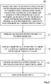
- Fig. 2 shows a flow diagram of the method for fabricating a magnetic device.
- the method 100 according to Fig. 2 comprises providing a layer stack such as that shown in Fig. 1A (110), heating the layer stack above the Neel temperature T N of the antiferromagnetic layer (120), applying a magnetic field H CL to the layer stack, the magnetic field H CL comprising a magnetic field direction having an arbitrary angle with respect to the easy axis (130), cooling the layer stack below the Néel temperature T N of the antiferromagnetic layer 15 with the magnetic field H CL applied (140), and finally removing the magnetic field H CL (150) .
- the magnetic device 300 shown in Fig. 1B comprises a layer stack 310 comprising a substrate 311, a first ferromagnetic layer 312 disposed on the substrate 311, the first ferromagnetic layer 312 comprising a first magnetization direction, a non-magnetic layer 313 disposed on the first ferromagnetic layer 312, a second ferromagnetic layer 314 disposed on the non-magnetic layer 313, the second ferromagnetic layer 314 comprising a second magnetization direction, and an antiferromagnetic layer 315 disposed on the second ferromagnetic layer 24, wherein the first and second magnetization directions are non-collinear including an arbitrary angle ⁇ .
- the exchange bias between the second ferromagnetic layer 314 and the antiferromagnetic layer 315 and the unidirectional anisotropy of the second ferromagnetic layer 314 disappear, such that M2 can align parallel to a relatively small magnetic field H CL .
- the direction of the unidirectional axis is defined by the magnetization vector M2 during cooling below T N , which in turn is defined by the field H CL applied during cooling.
- the first ferromagnetic layer 212 deposited on the substrate 211 with an optional buffer layer 216 has uniaxial anisotropy with the direction of the easy axis shown by the black arrow with caption EA.
- the second ferromagnetic layer 214 and the antiferromagnetic layer 215 form an exchange bias pair.
- an external magnetic field H CL is applied at an angle ⁇ with respect to EA. The system then is cooled below T N in the magnetic field H CL .
- the magnetization vector M1 of the first ferromagnetic layer 212 will turn towards the direction of EA while the magnetization M2 of the second ferromagnetic layer 214 will stay along the direction of H CL , due to the exchange bias.
- the first and second ferromagnetic layers 212 and 214 of Fig. 1A will become the first and second ferromagnetic layers 312 and 314 of Fig. 1B .
- the remanent state will be characterized by the non-collinear alignment of M1 and M2 with the angle ⁇ .
- the above-mentioned procedure allows to create a non-volatile device with a well-defined degree of non-collinearity.
- the advantage of this method is that the non-collinear angle ⁇ between M1 and M2 can be set at arbitrary values between -90° and 90° (measured either from M1 to M2 or vice versa) in a reproducible and accurate way.
- the angle ⁇ is changed by, for example, heating above T N , followed by cooling in the field with the required orientation.
- Another advantage of the method is a wide range of materials for the first and second ferromagnetic layers and the antiferromagnetic layer, which allows the system to be used in various applications. By choosing an antiferromagnetic layer with proper T N , the operation temperature of the device is adapted to specific applications.
- IrMn 3 with T N > 300K as antiferromagnetic layer allows for preparation of devices working at room temperature.
- superconductors for the first and/or second non-magnetic layers superconducting non-collinear spin valves or triplet Josephson junctions with variable and arbitrary ⁇ can be designed.
- the antiferromagnetic layer comprises a Neel temperature T N which is less than a Curie temperature T M of the first ferromagnetic layer and the second ferromagnetic layer.
- the antiferromagnetic layer like IrMn 3 as mentioned above comprises a Neel temperature T N which is greater than 300 K.
- it should be mentioned here that it is also possible to use an antiferromagnetic layer comprising a Neel temperature T N below 300 K.
- niobium was used as buffer layer (layer 216 or 316) and spacer layer (layer 213 or 313), both with the same thickness X.
- X was varied between 6 nm and 14 nm, where in the following text X is also used to label the samples as sX.
- Niobium is a non-magnetic metal and a superconductor for X>6nm.
- As the antiferromagnetic layer CoO(20nm) with T N 290K was deposited on top of the structure.
- Our prior experiment has shown a strong exchange bias field H eb ⁇ -1.3kOe for the single bilayer Co(2nm)/CoO(20nm).
- a is almost rectangular while the hysteresis for H
- b is S-shaped with strongly suppressed remanent moment.
- b, after cooling the samples in the field H CL -4.5kOe.
- the latter also oriented
- Strong splitting of the NSF curves is observed, but no SF scattering apart from the background intensity caused by the 99% efficiency of spin-analyzer (this means that 1% of the NSF intensity leaks to the SF channels).
- Such a scattering pattern evidences pure collinear magnetic alignment.
- the experiment proves the existence of a non-collinear state in the prototype sample, which is easy to control by choosing the direction of the magnetic field H CL applied during cooling.
- magnetizing field H CL has to be larger than the anisotropy of the second ferromagnetic layer.
- the latter can be close to zero by proper design of the sputtering process.
- the orientation of the second ferromagnetic layer can be achieved by a weak field.
- samples with X>10nm showed presence of superconductivity with transition temperature above 3K.
- the layer scheme used for the present test experiment also enables the design of superconducting non-collinear spin valves.
- the robustness of the system is given by the exchange bias field of the second ferromagnetic/antiferromagnetic bilayer (>1kOe) and the anisotropy field of the first ferromagnetic layer (approximately 50 Oe for the prototype).
- the latter value can also be tuned by the sputtering process and/or layer design.
Landscapes
- Engineering & Computer Science (AREA)
- Chemical & Material Sciences (AREA)
- Crystallography & Structural Chemistry (AREA)
- Power Engineering (AREA)
- Manufacturing & Machinery (AREA)
- Physics & Mathematics (AREA)
- Nanotechnology (AREA)
- Ceramic Engineering (AREA)
- Thermal Sciences (AREA)
- Spectroscopy & Molecular Physics (AREA)
- Thin Magnetic Films (AREA)
Abstract
A method (100) for fabricating a magnetic device comprises providing a layer stack (110), the layer stack comprising a substrate,
a first ferromagnetic layer disposed above the substrate, the first ferromagnetic layer comprising a uniaxial magnetic anisotropy including an easy axis,
a non-magnetic layer disposed on the first ferromagnetic layer,
a second ferromagnetic layer disposed on the non-magnetic layer, the second ferromagnetic layer comprising a unidirectional anisotropy, and
an antiferromagnetic layer disposed on the second ferromagnetic layer, the antiferromagnetic layer comprising a Neel temperature TN;
heating the layer stack above the Neel temperature TN of the antiferromagnetic layer (120);
applying a magnetic field HCL to the layer stack, the magnetic field HCL comprising a magnetic field direction having an arbitrary angle with respect to the easy axis (130);
cooling the layer stack below the Neel temperature TN of the antiferromagnetic layer with the magnetic field HCL applied; removing the magnetic field HCL.
a first ferromagnetic layer disposed above the substrate, the first ferromagnetic layer comprising a uniaxial magnetic anisotropy including an easy axis,
a non-magnetic layer disposed on the first ferromagnetic layer,
a second ferromagnetic layer disposed on the non-magnetic layer, the second ferromagnetic layer comprising a unidirectional anisotropy, and
an antiferromagnetic layer disposed on the second ferromagnetic layer, the antiferromagnetic layer comprising a Neel temperature TN;
heating the layer stack above the Neel temperature TN of the antiferromagnetic layer (120);
applying a magnetic field HCL to the layer stack, the magnetic field HCL comprising a magnetic field direction having an arbitrary angle with respect to the easy axis (130);
cooling the layer stack below the Neel temperature TN of the antiferromagnetic layer with the magnetic field HCL applied; removing the magnetic field HCL.
Description
- The present disclosure is related in general to the technical field of magnetic spin valve devices and in particular to a method for fabricating a magnetic device, a magnetic device in a state before carrying out the method, and a magnetic device in a state after carrying out the method.
- The spin valve (SV) is an essential building block of many spintronic devices. A typical SV consists of two ferromagnetic (FM) layers separated by a non-magnetic layer N. The typical thickness of the F and N layers in a SV is in the order of 1-10nm. The electrical resistance of a SV strongly depends on the mutual alignment of the magnetization vectors M1 and M2 of F1 and F2 layers: for antiparallel (AP) alignment, the resistance of the structure exhibits a maximum value, while for parallel (P) alignment the resistance is minimum. Thus, the SV is analog to a transistor in conventional resistive electronics. In order to enable switching between AP and P states, the magnetization M2 is pinned by a strong exchange bias (EB) field to an antiferromagnet, while M1 has a small magnetic anisotropy and can be switched without affecting M2.
- A classical SV requires switching between two collinear AP and P states, i.e. it is a digital devices so that the scope of possible applications is rather limited. For these and other reasons there is a need for the presence disclosure.
- A first aspect of the present disclosure is related to a method for fabricating a magnetic device, the method comprising providing a layer stack, the layer stack comprising a substrate, a first ferromagnetic layer disposed above the substrate, the first ferromagnetic layer comprising a uniaxial magnetic anisotropy including an easy axis, a non-magnetic layer disposed on the first ferromagnetic layer, a second ferromagnetic layer disposed on the non-magnetic layer, the second ferromagnetic layer comprising a unidirectional anisotropy, and an antiferromagnetic layer disposed on the second ferromagnetic layer, the antiferromagnetic layer comprising a Neel temperature TN;
heating the layer stack above the Neel temperature TN of the antiferromagnetic layer;
applying a magnetic field HCL to the layer stack, the magnetic field HCL comprising a magnetic field direction having an arbitrary angle with respect to the easy axis;
cooling the layer stack below the Neel temperature TN of the antiferromagnetic layer with the magnetic field HCL applied; and
removing the magnetic field HCL. - A second aspect of the present disclosure is related to a magnetic device, the magnetic device comprising providing a layer stack, the layer stack comprising a substrate, a first ferromagnetic layer disposed above the substrate, the first ferromagnetic layer comprising a uniaxial magnetic anisotropy including an easy axis, a non-magnetic layer disposed on the first ferromagnetic layer, a second ferromagnetic layer disposed on the non-magnetic layer, the second ferromagnetic layer comprising a unidirectional anisotropy, and an antiferromagnetic layer disposed on the second ferromagnetic layer.
- A third aspect of the present disclosure is related to a magnetic device, comprising a layer stack comprising a substrate, a first ferromagnetic layer disposed on the substrate, the first ferromagnetic layer comprising a first magnetization direction, a non-magnetic layer disposed on the first ferromagnetic layer, a second ferromagnetic layer disposed on the non-magnetic layer, the second ferromagnetic layer comprising a second magnetization direction, and an antiferromagnetic layer disposed on the second ferromagnetic layer; wherein the first and second magnetization directions are non-collinear including an arbitrary angle between them.
- A forth aspect of the present disclosure is related to a use of a magnetic device according to the third aspect in one or more of an electronic device, an electronic switching device, a spin valve device, a triplet spin valve device, a multiple state electronic device, a multiple state resistor, a multiple state memory cell, a synapse in an artificial neuron network, a superconducting spintronic device, a Josephson junction, or a triplet Josephson junction.
- The possibility to fix the magnetic configuration in an intermediate non-collinear (NC) state with an arbitrary angle between M1 and M2 will significantly expand the capabilities of the SV. Such a multiple state resistor can be used, for example, as a multi-state memory cell, or a synapse in artificial neuron networks. In addition, heterostructures consisting of NC ferromagnets and superconductors are promising systems in superconducting spintronics. Thus, the technical problem this proposal aims to solve is the creation of a non-volatile magnetic state with a controlled level of non-collinearity, this means with a well-defined angle.
- The accompanying drawings are included to provide a further understanding of embodiments and are incorporated in and constitute a part of this specification. The drawings illustrate embodiments and together with the description serve to explain principles of embodiments. Other embodiments and many of the intended advantages of embodiments will be readily appreciated as they become better understood by reference to the following detailed description.
- The elements of the drawings are not necessarily to scale relative to each other. Like reference numerals designate corresponding similar parts.
-
Fig. 1 comprisesFig. 1A and 1B and shows a perspective view of the magnetic device in its initial state before carrying out the method (A) and a perspective view of the magnetic device in its final state after carrying out the method (B). -
Fig. 2 shows a flow diagram of the method for fabricating a magnetic device. -
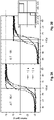
Fig. 3 comprisesFig. 3A and 3B and shows hysteresis loops measured on the sample s6 at room temperature (A) and at T = 13 K after cooling of the sample in HCL = - 4.5 kOe (B). The insert inFig. 3B shows the hysteresis loop in the range of fields ± 5 kOe. -
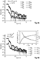
Fig. 4 comprisesFig. 4A and 4B and shows PNR data measures at 13K with external field H = 100 OE (A) and H = 10 Oe (B). Left insets show the magnetic configuration at the corresponding magnetic field obtained from numerical analysis of the PNR data, The right inset inFig. 4B shows the H-dependence of waveguide enhanced spin-flip scattering (full circles) and NC angle Δα (open circles). - In the following detailed description, reference is made to the accompanying drawings, which form a part hereof, and in which is shown by way of illustration specific embodiments in which the disclosure may be practiced. In this regard, directional terminology, such as "top", "bottom", "front", "back", "leading", "trailing", etc., is used with reference to the orientation of the Figure(s) being described. Because components of embodiments can be positioned in a number of different orientations, the directional terminology is used for purposes of illustration and is in no way limiting. It is to be understood that other embodiments may be utilized and structural or logical changes may be made without departing from the scope of the present disclosure. The following detailed description, therefore, is not to be taken in a limiting sense, and the scope of the present disclosure is defined by the appended claims.
- It is to be understood that the features of the various exemplary embodiments described herein may be combined with each other, unless specifically noted otherwise.
- As employed in this specification, the terms "bonded", "attached", "connected", "coupled" and/or "electrically connected/electrically coupled" are not meant to mean that the elements or layers must directly be contacted together; intervening elements or layers may be provided between the "bonded", "attached", "connected", "coupled" and/or "electrically connected/electrically coupled" elements, respectively. However, in accordance with the disclosure, the above-mentioned terms may, optionally, also have the specific meaning that the elements or layers are directly contacted together, i.e. that no intervening elements or layers are provided between the "bonded", "attached", "connected", "coupled" and/or "electrically connected/electrically coupled" elements, respectively.
- Further, the word "over" used with regard to a part, element or material layer formed or located "over" a surface may be used herein to mean that the part, element or material layer be located (e.g. placed, formed, deposited, etc.) "indirectly on" the implied surface with one or more additional parts, elements or layers being arranged between the implied surface and the part, element or material layer. However, the word "over" used with regard to a part, element or material layer formed or located "over" a surface may, optionally, also have the specific meaning that the part, element or material layer be located (e.g. placed, formed, deposited, etc.) "directly on", e.g. in direct contact with, the implied surface.
-
Fig. 1 comprisesFig. 1A and 1B and shows a perspective view of the magnetic device in its initial state before carrying out the method (A) and a perspective view of the magnetic device in its final state after carrying out the method (B). - The
magnetic device 200 as shown inFig. 1A comprises alayer stack 210 comprising asubstrate 211, a firstferromagnetic layer 212 disposed above thesubstrate 211, the firstferromagnetic layer 212 comprising a uniaxial magnetic anisotropy including an easy axis, anon-magnetic layer 213 disposed on the firstferromagnetic layer 212, a secondferromagnetic layer 214 disposed on thenon-magnetic layer 213, the secondferromagnetic layer 214 comprising a unidirectional anisotropy, and anantiferromagnetic layer 215 disposed on the secondferromagnetic layer 214. - The first and second
ferromagnetic layers non-magnetic spacer layer 213 disposed between them. The firstferromagnetic layer 212 is deposited on thesubstrate 211 with an optionalnon-magnetic buffer layer 216 disposed them. The first ferromagnetic layer 12 has an easy magnetic axis due to uniaxial magnetic anisotropy, which can be induced by the choice of substrate, the growth conditions, or by the shape anisotropy of the device. The secondferromagnetic layer 214 forms an exchange bias pair with theantiferromagnetic layer 215. The Neel temperature TN of theantiferromagnetic layer 215 is chosen to be lower than the Curie temperature TM of the secondferromagnetic layer 214. The exchange bias effect occurs between the neighboringantiferromagnetic layer 215 and the secondferromagnetic layer 214 at a temperature T with T < TN. It induces a unidirectional anisotropy (UD) in the secondferromagnetic layer 214, such that the direction of the magnetization M2 can only be altered by a strong field larger than the exchange bias field HEB. The latter is in the order of tens of Oe to several kOe, depending on the layer materials. -
Fig. 2 shows a flow diagram of the method for fabricating a magnetic device. - The
method 100 according toFig. 2 comprises providing a layer stack such as that shown inFig. 1A (110), heating the layer stack above the Neel temperature TN of the antiferromagnetic layer (120), applying a magnetic field HCL to the layer stack, the magnetic field HCL comprising a magnetic field direction having an arbitrary angle with respect to the easy axis (130), cooling the layer stack below the Néel temperature TN of the antiferromagnetic layer 15 with the magnetic field HCL applied (140), and finally removing the magnetic field HCL (150) . - As a result of
method 100, a magnetic device such as that shown inFig. 1B is obtained. - The
magnetic device 300 shown inFig. 1B comprises alayer stack 310 comprising asubstrate 311, a firstferromagnetic layer 312 disposed on thesubstrate 311, the firstferromagnetic layer 312 comprising a first magnetization direction, anon-magnetic layer 313 disposed on the firstferromagnetic layer 312, a secondferromagnetic layer 314 disposed on thenon-magnetic layer 313, the secondferromagnetic layer 314 comprising a second magnetization direction, and anantiferromagnetic layer 315 disposed on the second ferromagnetic layer 24, wherein the first and second magnetization directions are non-collinear including an arbitrary angle Δα. - At T > TN the exchange bias between the second
ferromagnetic layer 314 and theantiferromagnetic layer 315 and the unidirectional anisotropy of the secondferromagnetic layer 314 disappear, such that M2 can align parallel to a relatively small magnetic field HCL. The direction of the unidirectional axis is defined by the magnetization vector M2 during cooling below TN, which in turn is defined by the field HCL applied during cooling. - Somewhat more specifically, defining or writing the non-collinear magnetization state with angle Δα requires the following steps:
- (i) The
antiferromagnetic layer 315 is heated above TN to remove the exchange bias between the secondferromagnetic layer 314 and theantiferromagnetic layer 315. - (ii) A relatively small magnetic field HCL is applied at an angle Δα with respect to the easy axis EA of the first
ferromagnetic layer 312. - (iii) The system is cooled below TN with the magnetic field HCL applied. The magnetization direction of the second
ferromagnetic layer 314 will stay parallel to HCL during cooling, and the direction of the unidirectional anisotropy will be defined by M2. - (iv) Finally the magnetic field HCL is removed. M2 is now stabilized by the exchange bias, and stays in the direction previously defined by HCL- In this latter step after removing HCL, M1 in the first
ferromagnetic layer 312 aligns along the easy axis EA, such that in this remanent state (T < TN, H = 0) the angle between M1 and M2 corresponds to the requested angle Δα. The angle Δα affects the electrical resistance of the layer system, such that the readout of the state is performed by measuring the resistance of the device, either in current-in-plane or current-perpendicular-to-plane mode. - Referring again to
Fig. 1A , the firstferromagnetic layer 212 deposited on thesubstrate 211 with anoptional buffer layer 216 has uniaxial anisotropy with the direction of the easy axis shown by the black arrow with caption EA. The secondferromagnetic layer 214 and theantiferromagnetic layer 215 form an exchange bias pair. According toFig. 1A , above the Neel temperature TN of theantiferromagnetic layer 215 an external magnetic field HCL is applied at an angle Δα with respect to EA. The system then is cooled below TN in the magnetic field HCL. After release of the magnetic field HCL to zero, the magnetization vector M1 of the firstferromagnetic layer 212 will turn towards the direction of EA while the magnetization M2 of the secondferromagnetic layer 214 will stay along the direction of HCL, due to the exchange bias. The first and secondferromagnetic layers Fig. 1A will become the first and secondferromagnetic layers Fig. 1B . Thus according toFig. 1B the remanent state will be characterized by the non-collinear alignment of M1 and M2 with the angle Δα. - In summary, the above-mentioned procedure allows to create a non-volatile device with a well-defined degree of non-collinearity.
- The advantage of this method is that the non-collinear angle Δα between M1 and M2 can be set at arbitrary values between -90° and 90° (measured either from M1 to M2 or vice versa) in a reproducible and accurate way. The angle Δα is changed by, for example, heating above TN, followed by cooling in the field with the required orientation. Another advantage of the method is a wide range of materials for the first and second ferromagnetic layers and the antiferromagnetic layer, which allows the system to be used in various applications. By choosing an antiferromagnetic layer with proper TN, the operation temperature of the device is adapted to specific applications. For example, by choosing IrMn3 with TN > 300K as antiferromagnetic layer allows for preparation of devices working at room temperature. By choosing superconductors for the first and/or second non-magnetic layers, superconducting non-collinear spin valves or triplet Josephson junctions with variable and arbitrary Δα can be designed.
- According to an embodiment of the magnetic devices and the method of the first to forth aspects, the antiferromagnetic layer comprises a Neel temperature TN which is less than a Curie temperature TM of the first ferromagnetic layer and the second ferromagnetic layer. According to a further embodiment the antiferromagnetic layer like IrMn3 as mentioned above comprises a Neel temperature TN which is greater than 300 K. However, it should be mentioned here that it is also possible to use an antiferromagnetic layer comprising a Neel temperature TN below 300 K.
- To test the feasibility of the proposed approach we produced a series of samples of nominal composition Nb(X)/Co(1.5nm)/Nb(X)/Co(2nm)/CoO(20nm). The samples were deposited on Al2O3 (1102) substrate by magnetron sputtering. This R-plane sapphire substrate is characterized by the presence of an anisotropic surface profile, which induces uniaxial anisotropy in the subsequent magnetic layers, even through relatively thick buffer layers. It has been previously shown that uniaxial anisotropy was induced by the sapphire substrate in a magnetic Ni layer through a 100nm
thick V 203 buffer. For the prototype system discussed here, niobium was used as buffer layer (layer 216 or 316) and spacer layer (layer 213 or 313), both with the same thickness X. For the different samples, X was varied between 6 nm and 14 nm, where in the following text X is also used to label the samples as sX. Niobium is a non-magnetic metal and a superconductor for X>6nm. Cobalt was chosen for the first and second ferromagnetic layers 12 and 14 as a strong ferromagnet with bulk Tm = 1400K. As the antiferromagnetic layer CoO(20nm) with TN=290K was deposited on top of the structure. Our prior experiment has shown a strong exchange bias field Heb ∼ -1.3kOe for the single bilayer Co(2nm)/CoO(20nm). -
Fig. 3 shows the magnetic hysteresis loops measured on sample s6 (X=6nm) at room temperature (A) and at T=13K (B). In this experiment the magnetic field H was applied parallel to the surface along one of the edges of the square shaped substrates, denoted as a and b. Measurements at 13K were performed after cooling of the sample in a magnetic field of HCL = -4.5kOe. The hysteresis loop inFig. 3a shows that both FM layers are saturated for H > Hsat = 50 Oe. The hysteresis loop for H| | a is almost rectangular while the hysteresis for H | | b is S-shaped with strongly suppressed remanent moment. This observation evidences the presence of UA, with the easy axis close to a. We indeed expect from the known substrate surface structure, that the easy axis is offset from direction a by the angle of 20°, which explains the small drop of the remanent magnetization in the H | | a loop. After cooling the sample to T=13K the hysteresis loop shifts downwards along the vertical axis by a value Δm = -15µemu. The shift originates from the moment of the second ferromagnetic layer which is pinned to the antiferromagnetic layer and ±75Oe field is not enough to change the direction of M2. Our previous experiment shows that a strong field in the order of 4kOe is required to switch the direction of M2 (see inset inFig. 3b ). - For the quantitative characterization of the non-collinearity Δα we performed polarized neutron reflectometry (PNR) experiments. We measured two non-spin-flip (NSF) reflectivity channels R++ and R-- and two spin-flip (SF) channels R+- and R-+. Here the first (second) superscript sign denotes the spin direction of the incident (reflected) neutron spins. The presence of an asymmetry of the NSF curves S ≡ (R++ - R--)/(R++ + R--) evidences a magnetization structure with Ml, M2 collinear to external field magnetization, while non-zero SF scattering indicates the presence of non-collinear magnetization in the system. An analysis of all scattering channels provides quantitative information both about the magnetic depth profile of the in-plane magnetization vector.
-
Fig. 4A shows all four reflectivity channels measured at T=13K in a magnetic field H=100 Oe | | b, after cooling the samples in the field HCL = -4.5kOe. The latter also oriented | | b. Strong splitting of the NSF curves is observed, but no SF scattering apart from the background intensity caused by the 99% efficiency of spin-analyzer (this means that 1% of the NSF intensity leaks to the SF channels). Such a scattering pattern evidences pure collinear magnetic alignment. A numerical analysis of the PNR data shows that M1 and M2 are aligned antiparallel and collinear to the external field (see inset inFig. 4A ), so that at H=100 Oe the angle Δα=180°. This quantitative analysis is also in agreement with the hysteresis curve inFig. 3B , where for M1 a small coercivity << 100 Oe is observed, while the bias on the M2 hysteresis is ∼ 1.3kG, such that at H=100 Oe M1 follows the field direction, but M2 is not affected and stays as defined during the cooling. - Reducing the field to H=10 Oe (
Fig. 4B ) leads to a spin-flip signal with a strong peak close to the critical edge of total reflection, a so-called waveguide enhanced SF scattering. The inset inFig. 4B shows the field evolution of the SF intensity of this waveguide peak. Numerical analysis of these data shows a rotation of the magnetization M1 by α1 = 40±5° towards its easy axis, while M2 again remains in the direction defined during cooling. Thus M1 and M2 are now in a NC alignment with Δα = 140° (insetFig. 4B ). By using the relation ISF ∼ (sin α1)2 we can reconstruct the Δα(H) behavior, shown in the inset ofFig. 4B . By extrapolating this line to H=0 we can estimate remanent value Δα = 120°, which agrees within the experimental accuracy with SQUID data. - In summary, the experiment proves the existence of a non-collinear state in the prototype sample, which is easy to control by choosing the direction of the magnetic field HCL applied during cooling. We point out that magnetizing field HCL has to be larger than the anisotropy of the second ferromagnetic layer. The latter can be close to zero by proper design of the sputtering process. Thus, the orientation of the second ferromagnetic layer can be achieved by a weak field. We also observed that the NC magnetic state and thus the anisotropy of the first ferromagnetic layer persisted for all samples up to the thickest first ferromagnetic layer (X=14nm). Moreover, samples with X>10nm showed presence of superconductivity with transition temperature above 3K. Thus the layer scheme used for the present test experiment also enables the design of superconducting non-collinear spin valves. The robustness of the system is given by the exchange bias field of the second ferromagnetic/antiferromagnetic bilayer (>1kOe) and the anisotropy field of the first ferromagnetic layer (approximately 50 Oe for the prototype). The latter value can also be tuned by the sputtering process and/or layer design.
- In addition, while a particular feature or aspect of an embodiment of the disclosure may have been disclosed with respect to only one of several implementations, such feature or aspect may be combined with one or more other features or aspects of the other implementations as may be desired and advantageous for any given or particular application. Furthermore, to the extent that the terms "include", "have", "with", or other variants thereof are used in either the detailed description or the claims, such terms are intended to be inclusive in a manner similar to the term "comprise". Furthermore, it should be understood that embodiments of the disclosure may be implemented in discrete circuits, partially integrated circuits or fully integrated circuits or programming means. Also, the term "exemplary" is merely meant as an example, rather than the best or optimal. It is also to be appreciated that features and/or elements depicted herein are illustrated with particular dimensions relative to one another for purposes of simplicity and ease of understanding, and that actual dimensions may differ substantially from that illustrated herein.
- Although specific embodiments have been illustrated and described herein, it will be appreciated by those of ordinary skill in the art that a variety of alternate and/or equivalent implementations may be substituted for the specific embodiments shown and described without departing from the scope of the present disclosure. This application is intended to cover any adaptations or variations of the specific embodiments discussed herein. Therefore, it is intended that this disclosure be limited only by the claims and the equivalents thereof.
Claims (16)
- A method (100) for fabricating a magnetic device, the method comprising
providing a layer stack (110), the layer stack comprisinga substrate,a first ferromagnetic layer disposed above the substrate, the first ferromagnetic layer comprising a uniaxial magnetic anisotropy including an easy axis,a non-magnetic layer disposed on the first ferromagnetic layer,a second ferromagnetic layer disposed on the non-magnetic layer, the second ferromagnetic layer comprising a unidirectional anisotropy, andan antiferromagnetic layer disposed on the second ferromagnetic layer, the antiferromagnetic layer comprising a Neel temperature TN;heating the layer stack above the Neel temperature TN of the antiferromagnetic layer (120);
applying a magnetic field HCL to the layer stack, the magnetic field HCL comprising a magnetic field direction having an arbitrary angle with respect to the easy axis (130);
cooling the layer stack below the Neel temperature TN of the antiferromagnetic layer with the magnetic field HCL applied (140); and
removing the magnetic field HCL (150). - The method according to claim 1, wherein
the antiferromagnetic layer (16) comprises a Neel temperature TN which is less than a Curie temperature TM of the second ferromagnetic layer (14). - The method according to claim 1 or 2, wherein
the antiferromagnetic layer (16) comprises a Neel temperature TN which is greater than 300 K. - The method according to any one of the preceding claims, further comprising
providing the layer stack (10) with a non-magnetic buffer layer (16) between the substrate (11) and the first ferromagnetic layer (12). - A magnetic device (200) comprising
a layer stack (210) comprising
a substrate (211),
a first ferromagnetic layer (212) disposed above the substrate (211), the first ferromagnetic layer (212) comprising a uniaxial magnetic anisotropy including an easy axis,
a non-magnetic layer (213) disposed on the first ferromagnetic layer (212),
a second ferromagnetic layer (214) disposed on the non-magnetic layer (213), the second ferromagnetic layer (214) comprising a unidirectional anisotropy, and
an antiferromagnetic layer (215) disposed on the second ferromagnetic layer (214). - The magnetic device (200) according to claim 5, wherein the antiferromagnetic layer (215) comprises a Neel temperature TN which is less than a Curie temperature TM of the second ferromagnetic layer (214).
- The magnetic device (200) according to claim 5 or 6, wherein
the antiferromagnetic layer (215) comprises a Neel temperature TN which is greater than 300 K. - The magnetic device (200) according to any one of claims 5 to 7, further comprising
a non-magnetic buffer layer (216) disposed between the substrate (211) and the first ferromagnetic layer (212). - The magnetic device (200) according to any one of claims 5 to 7 or 8, wherein
one or both of the non-magnetic layer (213) and the non-magnetic buffer layer (216) comprises a superconducting material. - A magnetic device (300), comprising
a layer stack (310) comprising
a substrate (311),
a first ferromagnetic layer (312) disposed on the substrate (311), the first ferromagnetic layer (312) comprising a first magnetization direction,
a non-magnetic layer (313) disposed on the first ferromagnetic layer (312),
a second ferromagnetic layer (314) disposed on the non-magnetic layer (313), the second ferromagnetic layer (314) comprising a second magnetization direction, and
an antiferromagnetic layer (315) disposed on the second ferromagnetic layer (314); wherein
the first and second magnetization directions are non-collinear including an arbitrary angle between them. - The magnetic device (300) according to claim 10, wherein the first ferromagnetic layer (312) comprises a uniaxial magnetic anisotropy; and
the second ferromagnetic layer (314) comprises a unidirectional anisotropy. - The magnetic device (300) according to claim 10 or 11, wherein
the antiferromagnetic layer (315) comprises a Neel temperature TN which is less than a Curie temperature TM of the second ferromagnetic layer (314). - The magnetic device (300) according to any one of claims 10 to 12, wherein
the antiferromagnetic layer (315) comprises a Neel temperature TN which is greater than 300 K. - The magnetic device (300) according to any one of claims 10 to 13, further comprising
a non-magnetic buffer layer (316) disposed between the substrate (311) and the first ferromagnetic layer (312). - The magnetic device (200) according to any one of claims 10 to 13 or 14, wherein
one or both of the non-magnetic layer (313) and the non-magnetic buffer layer (316) comprises a superconducting material. - Use of a magnetic device according to any one of claims 10 to 15 in one or more of- an electronic device,- an electronic switching device,- a spin valve device,- a triplet spin valve device,- a multiple state electronic device,- a multiple state resistor,- a multiple state memory cell,- a synapse in an artificial neuron network,- a superconducting spintronic device,- a Josephson junction, or- a triplet Josephson junction.
Priority Applications (4)
| Application Number | Priority Date | Filing Date | Title |
|---|---|---|---|
| EP21153254.4A EP4033503A1 (en) | 2021-01-25 | 2021-01-25 | A method for fabricating a magnetic spin valve device comprising ferromagnetic layers with non-collinear magnetizations |
| PCT/EP2022/051081 WO2022157170A1 (en) | 2021-01-25 | 2022-01-19 | A method for fabricating a magnetic spin valve device comprising ferromagnetic layers with non-collinear magnetizations |
| EP22702888.3A EP4281987A1 (en) | 2021-01-25 | 2022-01-19 | A method for fabricating a magnetic spin valve device comprising ferromagnetic layers with non-collinear magnetizations |
| US18/262,761 US20240415023A1 (en) | 2021-01-25 | 2022-01-19 | A method for fabricating a magnetic spin valve device comprising ferromagnetic layers with non-collinear magnetizations |
Applications Claiming Priority (1)
| Application Number | Priority Date | Filing Date | Title |
|---|---|---|---|
| EP21153254.4A EP4033503A1 (en) | 2021-01-25 | 2021-01-25 | A method for fabricating a magnetic spin valve device comprising ferromagnetic layers with non-collinear magnetizations |
Publications (1)
| Publication Number | Publication Date |
|---|---|
| EP4033503A1 true EP4033503A1 (en) | 2022-07-27 |
Family
ID=74285199
Family Applications (2)
| Application Number | Title | Priority Date | Filing Date |
|---|---|---|---|
| EP21153254.4A Withdrawn EP4033503A1 (en) | 2021-01-25 | 2021-01-25 | A method for fabricating a magnetic spin valve device comprising ferromagnetic layers with non-collinear magnetizations |
| EP22702888.3A Pending EP4281987A1 (en) | 2021-01-25 | 2022-01-19 | A method for fabricating a magnetic spin valve device comprising ferromagnetic layers with non-collinear magnetizations |
Family Applications After (1)
| Application Number | Title | Priority Date | Filing Date |
|---|---|---|---|
| EP22702888.3A Pending EP4281987A1 (en) | 2021-01-25 | 2022-01-19 | A method for fabricating a magnetic spin valve device comprising ferromagnetic layers with non-collinear magnetizations |
Country Status (3)
| Country | Link |
|---|---|
| US (1) | US20240415023A1 (en) |
| EP (2) | EP4033503A1 (en) |
| WO (1) | WO2022157170A1 (en) |
Citations (3)
| Publication number | Priority date | Publication date | Assignee | Title |
|---|---|---|---|---|
| US20030179511A1 (en) * | 2002-03-25 | 2003-09-25 | Gang Xiao | Reduction of noise, and optimization of magnetic field sensitivity and electrical properties in magnetic tunnel junction devices |
| US20040087037A1 (en) * | 2002-10-31 | 2004-05-06 | Honeywell International Inc. | Etch-stop material for improved manufacture of magnetic devices |
| RU2442245C1 (en) * | 2010-11-17 | 2012-02-10 | Научно-учебное учреждение Научно-исследовательский институт ядерной физики имени Д.В. Скобельцына Московского государственного университета имени М.В. Ломоносова | Solar photoelectric submodule |
-
2021
- 2021-01-25 EP EP21153254.4A patent/EP4033503A1/en not_active Withdrawn
-
2022
- 2022-01-19 EP EP22702888.3A patent/EP4281987A1/en active Pending
- 2022-01-19 WO PCT/EP2022/051081 patent/WO2022157170A1/en not_active Ceased
- 2022-01-19 US US18/262,761 patent/US20240415023A1/en active Pending
Patent Citations (3)
| Publication number | Priority date | Publication date | Assignee | Title |
|---|---|---|---|---|
| US20030179511A1 (en) * | 2002-03-25 | 2003-09-25 | Gang Xiao | Reduction of noise, and optimization of magnetic field sensitivity and electrical properties in magnetic tunnel junction devices |
| US20040087037A1 (en) * | 2002-10-31 | 2004-05-06 | Honeywell International Inc. | Etch-stop material for improved manufacture of magnetic devices |
| RU2442245C1 (en) * | 2010-11-17 | 2012-02-10 | Научно-учебное учреждение Научно-исследовательский институт ядерной физики имени Д.В. Скобельцына Московского государственного университета имени М.В. Ломоносова | Solar photoelectric submodule |
Non-Patent Citations (2)
| Title |
|---|
| FENG Z ET AL: "Out of plane superconducting Nb/Cu/Ni/Cu/Co triplet spin-valves", APPLIED PHYSICS LETTERS, A I P PUBLISHING LLC, US, vol. 111, no. 4, 24 July 2017 (2017-07-24), XP012220306, ISSN: 0003-6951, [retrieved on 20170724], DOI: 10.1063/1.4995434 * |
| YI ZHU ET AL: "Superconducting exchange coupling between ferromagnets", NATURE MATERIALS, vol. 16, no. 2, 19 September 2016 (2016-09-19), London, pages 195 - 199, XP055537087, ISSN: 1476-1122, DOI: 10.1038/nmat4753 * |
Also Published As
| Publication number | Publication date |
|---|---|
| WO2022157170A1 (en) | 2022-07-28 |
| US20240415023A1 (en) | 2024-12-12 |
| EP4281987A1 (en) | 2023-11-29 |
Similar Documents
| Publication | Publication Date | Title |
|---|---|---|
| US5959880A (en) | Low aspect ratio magnetoresistive tunneling junction | |
| US7750421B2 (en) | High performance MTJ element for STT-RAM and method for making the same | |
| US8912614B2 (en) | Magnetic tunnel junction devices having magnetic layers formed on composite, obliquely deposited seed layers | |
| US7570463B2 (en) | Magnetic tunnel junctions including crystalline and amorphous tunnel barrier materials | |
| US6483741B1 (en) | Magnetization drive method, magnetic functional device, and magnetic apparatus | |
| EP2404297A1 (en) | St-ram cells with perpendicular anisotropy | |
| US20250231259A1 (en) | Magnetorestistive sensor sensitive to an out-of-plane magnetic field | |
| US11922986B2 (en) | Magnetic heterojunction structure and method for controlling and achieving logic and multiple-state storage functions | |
| Higo et al. | Anisotropic tunneling magnetoresistance in GaMnAs/AlAs/GaMnAs ferromagnetic semiconductor tunnel junctions | |
| US6649423B2 (en) | Method for modifying switching field characteristics of magnetic tunnel junctions | |
| Philipp et al. | Large two-level magnetoresistance effect in doped manganite grain-boundary junctions | |
| Kabanov et al. | Asymmetric magnetization reversal of the Heusler alloy Co2FeSi as free layer in an CoFeB/MgO/Co2FeSi magnetic tunnel junction | |
| Isogami et al. | Inverse current-induced magnetization switching in magnetic tunnel junctions with Fe4N free layer | |
| EP1830410A1 (en) | Single-charge tunnelling device | |
| US6445024B1 (en) | Ramp-edge structured tunneling devices using ferromagnet electrodes | |
| US20240415023A1 (en) | A method for fabricating a magnetic spin valve device comprising ferromagnetic layers with non-collinear magnetizations | |
| Cartier et al. | Magnetic domain configurations in exchange-coupled NiO/Co bilayer films | |
| US9293184B2 (en) | Method of pinning domain walls in a nanowire magnetic memory device | |
| Flokstra et al. | Magnetic coupling in superconducting spin valves with strong ferromagnets | |
| Lee et al. | Strain-modulated exchange-spring magnetic behavior in amorphous Tb-Fe thin films | |
| US20050014295A1 (en) | Method of manufacture of a magneto-resistive device | |
| US10998131B2 (en) | Multilayer device having an improved antiferromagnetic pinning layer and a corresponding manufacturing method | |
| Iurchuk et al. | All-electrical operation of a Curie switch at room temperature | |
| Cuchet et al. | Field Dependence of Spin-Transfer Torque Switching Current in Perpendicular Magnetic Tunnel Junctions | |
| Willing et al. | Novel TMR sensor functionalities via oblique-incidence deposition |
Legal Events
| Date | Code | Title | Description |
|---|---|---|---|
| PUAI | Public reference made under article 153(3) epc to a published international application that has entered the european phase |
Free format text: ORIGINAL CODE: 0009012 |
|
| STAA | Information on the status of an ep patent application or granted ep patent |
Free format text: STATUS: REQUEST FOR EXAMINATION WAS MADE |
|
| 17P | Request for examination filed |
Effective date: 20210125 |
|
| AK | Designated contracting states |
Kind code of ref document: A1 Designated state(s): AL AT BE BG CH CY CZ DE DK EE ES FI FR GB GR HR HU IE IS IT LI LT LU LV MC MK MT NL NO PL PT RO RS SE SI SK SM TR |
|
| STAA | Information on the status of an ep patent application or granted ep patent |
Free format text: STATUS: THE APPLICATION IS DEEMED TO BE WITHDRAWN |
|
| 18D | Application deemed to be withdrawn |
Effective date: 20230128 |