EP4030876A1 - Substrate unit and manufacturing method of substrate unit - Google Patents
Substrate unit and manufacturing method of substrate unit Download PDFInfo
- Publication number
- EP4030876A1 EP4030876A1 EP21218123.4A EP21218123A EP4030876A1 EP 4030876 A1 EP4030876 A1 EP 4030876A1 EP 21218123 A EP21218123 A EP 21218123A EP 4030876 A1 EP4030876 A1 EP 4030876A1
- Authority
- EP
- European Patent Office
- Prior art keywords
- substrate
- connector
- unit
- terminal
- housing
- Prior art date
- Legal status (The legal status is an assumption and is not a legal conclusion. Google has not performed a legal analysis and makes no representation as to the accuracy of the status listed.)
- Granted
Links
Images




Classifications
-
- H—ELECTRICITY
- H05—ELECTRIC TECHNIQUES NOT OTHERWISE PROVIDED FOR
- H05K—PRINTED CIRCUITS; CASINGS OR CONSTRUCTIONAL DETAILS OF ELECTRIC APPARATUS; MANUFACTURE OF ASSEMBLAGES OF ELECTRICAL COMPONENTS
- H05K5/00—Casings, cabinets or drawers for electric apparatus
- H05K5/02—Details
- H05K5/0256—Details of interchangeable modules or receptacles therefor, e.g. cartridge mechanisms
-
- H—ELECTRICITY
- H01—ELECTRIC ELEMENTS
- H01R—ELECTRICALLY-CONDUCTIVE CONNECTIONS; STRUCTURAL ASSOCIATIONS OF A PLURALITY OF MUTUALLY-INSULATED ELECTRICAL CONNECTING ELEMENTS; COUPLING DEVICES; CURRENT COLLECTORS
- H01R12/00—Structural associations of a plurality of mutually-insulated electrical connecting elements, specially adapted for printed circuits, e.g. printed circuit boards [PCB], flat or ribbon cables, or like generally planar structures, e.g. terminal strips, terminal blocks; Coupling devices specially adapted for printed circuits, flat or ribbon cables, or like generally planar structures; Terminals specially adapted for contact with, or insertion into, printed circuits, flat or ribbon cables, or like generally planar structures
- H01R12/70—Coupling devices
- H01R12/71—Coupling devices for rigid printing circuits or like structures
- H01R12/712—Coupling devices for rigid printing circuits or like structures co-operating with the surface of the printed circuit or with a coupling device exclusively provided on the surface of the printed circuit
- H01R12/716—Coupling device provided on the PCB
-
- H—ELECTRICITY
- H05—ELECTRIC TECHNIQUES NOT OTHERWISE PROVIDED FOR
- H05K—PRINTED CIRCUITS; CASINGS OR CONSTRUCTIONAL DETAILS OF ELECTRIC APPARATUS; MANUFACTURE OF ASSEMBLAGES OF ELECTRICAL COMPONENTS
- H05K1/00—Printed circuits
- H05K1/02—Details
-
- H—ELECTRICITY
- H01—ELECTRIC ELEMENTS
- H01R—ELECTRICALLY-CONDUCTIVE CONNECTIONS; STRUCTURAL ASSOCIATIONS OF A PLURALITY OF MUTUALLY-INSULATED ELECTRICAL CONNECTING ELEMENTS; COUPLING DEVICES; CURRENT COLLECTORS
- H01R12/00—Structural associations of a plurality of mutually-insulated electrical connecting elements, specially adapted for printed circuits, e.g. printed circuit boards [PCB], flat or ribbon cables, or like generally planar structures, e.g. terminal strips, terminal blocks; Coupling devices specially adapted for printed circuits, flat or ribbon cables, or like generally planar structures; Terminals specially adapted for contact with, or insertion into, printed circuits, flat or ribbon cables, or like generally planar structures
- H01R12/50—Fixed connections
- H01R12/51—Fixed connections for rigid printed circuits or like structures
- H01R12/52—Fixed connections for rigid printed circuits or like structures connecting to other rigid printed circuits or like structures
-
- H—ELECTRICITY
- H01—ELECTRIC ELEMENTS
- H01R—ELECTRICALLY-CONDUCTIVE CONNECTIONS; STRUCTURAL ASSOCIATIONS OF A PLURALITY OF MUTUALLY-INSULATED ELECTRICAL CONNECTING ELEMENTS; COUPLING DEVICES; CURRENT COLLECTORS
- H01R13/00—Details of coupling devices of the kinds covered by groups H01R12/70 or H01R24/00 - H01R33/00
- H01R13/46—Bases; Cases
- H01R13/502—Bases; Cases composed of different pieces
- H01R13/506—Bases; Cases composed of different pieces assembled by snap action of the parts
-
- H—ELECTRICITY
- H01—ELECTRIC ELEMENTS
- H01R—ELECTRICALLY-CONDUCTIVE CONNECTIONS; STRUCTURAL ASSOCIATIONS OF A PLURALITY OF MUTUALLY-INSULATED ELECTRICAL CONNECTING ELEMENTS; COUPLING DEVICES; CURRENT COLLECTORS
- H01R43/00—Apparatus or processes specially adapted for manufacturing, assembling, maintaining, or repairing of line connectors or current collectors or for joining electric conductors
- H01R43/20—Apparatus or processes specially adapted for manufacturing, assembling, maintaining, or repairing of line connectors or current collectors or for joining electric conductors for assembling or disassembling contact members with insulating base, case or sleeve
- H01R43/205—Apparatus or processes specially adapted for manufacturing, assembling, maintaining, or repairing of line connectors or current collectors or for joining electric conductors for assembling or disassembling contact members with insulating base, case or sleeve with a panel or printed circuit board
-
- H—ELECTRICITY
- H05—ELECTRIC TECHNIQUES NOT OTHERWISE PROVIDED FOR
- H05K—PRINTED CIRCUITS; CASINGS OR CONSTRUCTIONAL DETAILS OF ELECTRIC APPARATUS; MANUFACTURE OF ASSEMBLAGES OF ELECTRICAL COMPONENTS
- H05K1/00—Printed circuits
- H05K1/02—Details
- H05K1/14—Structural association of two or more printed circuits
- H05K1/145—Arrangements wherein electric components are disposed between and simultaneously connected to two planar printed circuit boards, e.g. Cordwood modules
-
- H—ELECTRICITY
- H05—ELECTRIC TECHNIQUES NOT OTHERWISE PROVIDED FOR
- H05K—PRINTED CIRCUITS; CASINGS OR CONSTRUCTIONAL DETAILS OF ELECTRIC APPARATUS; MANUFACTURE OF ASSEMBLAGES OF ELECTRICAL COMPONENTS
- H05K3/00—Apparatus or processes for manufacturing printed circuits
- H05K3/36—Assembling printed circuits with other printed circuits
- H05K3/368—Assembling printed circuits with other printed circuits parallel to each other
-
- H—ELECTRICITY
- H05—ELECTRIC TECHNIQUES NOT OTHERWISE PROVIDED FOR
- H05K—PRINTED CIRCUITS; CASINGS OR CONSTRUCTIONAL DETAILS OF ELECTRIC APPARATUS; MANUFACTURE OF ASSEMBLAGES OF ELECTRICAL COMPONENTS
- H05K5/00—Casings, cabinets or drawers for electric apparatus
- H05K5/0026—Casings, cabinets or drawers for electric apparatus provided with connectors and printed circuit boards [PCB], e.g. automotive electronic control units
-
- H—ELECTRICITY
- H05—ELECTRIC TECHNIQUES NOT OTHERWISE PROVIDED FOR
- H05K—PRINTED CIRCUITS; CASINGS OR CONSTRUCTIONAL DETAILS OF ELECTRIC APPARATUS; MANUFACTURE OF ASSEMBLAGES OF ELECTRICAL COMPONENTS
- H05K5/00—Casings, cabinets or drawers for electric apparatus
- H05K5/0026—Casings, cabinets or drawers for electric apparatus provided with connectors and printed circuit boards [PCB], e.g. automotive electronic control units
- H05K5/0069—Casings, cabinets or drawers for electric apparatus provided with connectors and printed circuit boards [PCB], e.g. automotive electronic control units having connector relating features for connecting the connector pins with the PCB or for mounting the connector body with the housing
-
- H—ELECTRICITY
- H05—ELECTRIC TECHNIQUES NOT OTHERWISE PROVIDED FOR
- H05K—PRINTED CIRCUITS; CASINGS OR CONSTRUCTIONAL DETAILS OF ELECTRIC APPARATUS; MANUFACTURE OF ASSEMBLAGES OF ELECTRICAL COMPONENTS
- H05K5/00—Casings, cabinets or drawers for electric apparatus
- H05K5/02—Details
- H05K5/0217—Mechanical details of casings
-
- H—ELECTRICITY
- H05—ELECTRIC TECHNIQUES NOT OTHERWISE PROVIDED FOR
- H05K—PRINTED CIRCUITS; CASINGS OR CONSTRUCTIONAL DETAILS OF ELECTRIC APPARATUS; MANUFACTURE OF ASSEMBLAGES OF ELECTRICAL COMPONENTS
- H05K7/00—Constructional details common to different types of electric apparatus
- H05K7/02—Arrangements of circuit components or wiring on supporting structure
- H05K7/026—Multiple connections subassemblies
-
- H—ELECTRICITY
- H05—ELECTRIC TECHNIQUES NOT OTHERWISE PROVIDED FOR
- H05K—PRINTED CIRCUITS; CASINGS OR CONSTRUCTIONAL DETAILS OF ELECTRIC APPARATUS; MANUFACTURE OF ASSEMBLAGES OF ELECTRICAL COMPONENTS
- H05K7/00—Constructional details common to different types of electric apparatus
- H05K7/14—Mounting supporting structure in casing or on frame or rack
- H05K7/1422—Printed circuit boards receptacles, e.g. stacked structures, electronic circuit modules or box like frames
-
- H—ELECTRICITY
- H05—ELECTRIC TECHNIQUES NOT OTHERWISE PROVIDED FOR
- H05K—PRINTED CIRCUITS; CASINGS OR CONSTRUCTIONAL DETAILS OF ELECTRIC APPARATUS; MANUFACTURE OF ASSEMBLAGES OF ELECTRICAL COMPONENTS
- H05K7/00—Constructional details common to different types of electric apparatus
- H05K7/14—Mounting supporting structure in casing or on frame or rack
- H05K7/1422—Printed circuit boards receptacles, e.g. stacked structures, electronic circuit modules or box like frames
- H05K7/1427—Housings
-
- H—ELECTRICITY
- H05—ELECTRIC TECHNIQUES NOT OTHERWISE PROVIDED FOR
- H05K—PRINTED CIRCUITS; CASINGS OR CONSTRUCTIONAL DETAILS OF ELECTRIC APPARATUS; MANUFACTURE OF ASSEMBLAGES OF ELECTRICAL COMPONENTS
- H05K7/00—Constructional details common to different types of electric apparatus
- H05K7/14—Mounting supporting structure in casing or on frame or rack
- H05K7/1422—Printed circuit boards receptacles, e.g. stacked structures, electronic circuit modules or box like frames
- H05K7/1435—Expandable constructions
-
- H—ELECTRICITY
- H05—ELECTRIC TECHNIQUES NOT OTHERWISE PROVIDED FOR
- H05K—PRINTED CIRCUITS; CASINGS OR CONSTRUCTIONAL DETAILS OF ELECTRIC APPARATUS; MANUFACTURE OF ASSEMBLAGES OF ELECTRICAL COMPONENTS
- H05K7/00—Constructional details common to different types of electric apparatus
- H05K7/14—Mounting supporting structure in casing or on frame or rack
- H05K7/1438—Back panels or connecting means therefor; Terminals; Coding means to avoid wrong insertion
- H05K7/1452—Mounting of connectors; Switching; Reinforcing of back panels
Definitions
- the presently disclosed subject matter relates to a substrate unit and a method of manufacturing the substrate unit.
- a substrate on which an input unit or an output unit, a control circuit, a connector for connection to the electrical device, and the like are mounted is generally accommodated in a case (for example, JP2014-187123A ).
- the vehicle has various specifications, and the number of electrical devices to be mounted varies depending on the specifications. Therefore, it is necessary to design the substrate configuring the substrate unit for each specification.
- a substrate which includes input units or output units whose number meets a high-grade specification requirement is designed, and the substrate having the high-grade specification is mounted on a vehicle having a standard specification.
- the vehicle having a standard specification an unnecessary cost is generated due to an unused part of the substrate.
- an input unit or an output unit to be connected to a standard electrical device mounted in common in both the standard specification and the high-grade specification is provided on a base substrate (a first substrate), and an input unit or an output unit to be connected to an extended electrical device mounted only in the high-grade specification is provided on an extended substrate (a second substrate).
- the base substrate is mounted on the vehicle having a standard specification, and both the base substrate and the extended substrate are mounted on the vehicle having a high-grade specification.
- Illustrative aspects of the presently disclosed subject matter provide a substrate unit and a method of manufacturing the substrate unit configured to reduce the amount of work for coupling a first connector mounted on a first substrate, a second connector mounted on a second substrate, and an external connector.
- a substrate unit includes a first connector including a first terminal and a first housing accommodating the first terminal, and configured to be connected to an external connector, a first substrate on which the first connector is mounted and a case accommodating the first substrate.
- the first housing is provided with a first locking portion configured to be locked to a second housing of a second connector mounted on a second substrate.
- the first terminal is disposed to face an opening provided in the case through which the external connector is to be connected to the first connector.
- a substrate unit includes a first connector including a first terminal and a first housing accommodating the first terminal, and configured to be connected to an external connector, a first substrate on which the first connector is mounted, a second connector including a second terminal and a second housing accommodating the second terminal, and configured to be connected to the external connector, a second substrate on which the second connector is mounted and a case accommodating the first substrate and the second substrate.
- the first housing is provided with a first locking portion.
- the second housing is provided with a second locking portion. The first locking portion and the second locking portion are locked to each other.
- the first terminal and the second terminal are disposed to face an opening provided in the case through which the external connector is to be connected to the first connector and the second connector.
- a manufacturing method for manufacturing a substrate unit in which the substrate unit is either of a first substrate unit or a second substrate unit, includes preparing a first substrate on which a first connector is mounted, the first connector including a first terminal and a first housing accommodating the first terminal, the first housing being provided with a first locking portion, the first connector being configured to be connected to an external connector and a second substrate on which a second connector is mounted, the second connector including a second terminal and a second housing accommodating the second terminal, the second housing being provided with a second locking portion, the second connector being configured to be connected to the external connector and manufacturing the first substrate unit or the second substrate unit selectively according to which of a first specification or a second specification is selected.
- the first substrate unit is to be manufactured and the manufacturing of the first substrate unit includes accommodating only the first substrate into the case such that the first terminal faces an opening provided in the case through which the external connector is to be connected to the first connector and when the second specification is selected, the second substrate unit is to be manufactured and the manufacturing of the second substrate unit includes locking the first locking portion and the second locking portion with each other and accommodating both the first substrate and the second substrate into the case such that the first terminal and the second terminal face the opening provided in the case through which the external connector is to be connected to the first connector and the second connector.
- a substrate unit 1A (a second substrate unit) to be mounted on a vehicle having a high-grade specification (a second specification) and a substrate unit 1B (a first substrate unit) to be mounted on a vehicle having a standard specification (a first specification) are manufactured.
- the substrate unit 1A having a high-grade specification will be described with reference to FIGS. 1 to 5 .
- the substrate unit 1A having a high-grade specification includes a base substrate 2 for operating a standard electrical device (not shown), an extended substrate 3 for operating an extended electrical device (not shown), a connecting unit 4 for electrically connecting the base substrate 2 and the extended substrate 3, and a case 5 for accommodating the base substrate 2 and the extended substrate 3.
- the standard electrical device is an electrical device (for example, an air conditioner unit, a power window unit, or the like) that is attached in common to a vehicle having a high-grade specification and a vehicle having a standard specification.
- the extended electrical device is an electrical device that is selectively attached according to a specification of a vehicle.
- a connector (a first connector) 21 and the like are mounted on the base substrate 2.
- the connector 21 includes terminals (first terminals) 22 and a housing (first housing) 23 that accommodates the terminals.
- the terminal 22 is formed in a substantially L shape, one end thereof extending along a thickness direction D1 of the base substrate 2 is connected to the base substrate 2, and the other end thereof extending parallel to the base substrate 2 is accommodated in the housing 23.
- the other end of the terminal 22 is configured as, for example, a male terminal, and protrudes from the housing 23.
- the housing 23 is provided with locking projections 231 to be locked to a housing 33 of an extended connector 31 to be described later.
- the locking projections 231 (first locking portions) are provided on outer surfaces of the housing 23 facing in a direction orthogonal to both the thickness direction D1 and a direction along which the other end of the terminal 22 extends.
- the connector 21 is to be connected to an external connector (not shown) provided at an end of a wire harness.
- the wire harness is connected to a central ECU (host control device), a standard electrical device, and an extended electrical device (not shown).
- a control circuit 24, a power supply circuit 25, a communication interface (I/F) 26, and the like are mounted on the base substrate 2.
- the control circuit 24 includes, for example, a microcomputer having a CPU.
- the control circuit 24 communicates with the central ECU and controls the standard electrical device and the extended electrical device according to instructions from the central ECU.
- the power supply circuit 25 generates power for the control circuit 24 from power supplied via an external connector.
- the communication I/F 26 is a circuit that modulates and demodulates communication signals transmitted and received between the central ECU and the control circuit 24.
- Various circuits are mounted on the base substrate 2 according to a type of the standard electrical device, and the various circuits are connected to the control circuit 24.
- two input I/Fs 27 input units
- three output drives (DRVs) 28 output units
- the input I/F 27 is mounted with respect to the standard electrical device.
- the standard electrical device is a device, that operates based on an output from the control circuit 24, such as a motor or a lamp
- the output DRV 28 is mounted with respect to the standard electrical device.
- the power supply circuit 25, the communication I/F 26, the input I/Fs 27, and the output DRVs 28 are connected to the terminals 22, and when an external connector is connected to the terminals 22, the power supply circuit 25, the communication I/F 26, the input I/Fs 27, and the output DRVs 28 are connected to the central ECU and/or the standard electrical device.
- the base substrate 2 and the extended substrate 3 are stacked along the thickness direction D1.
- An extended connector (a second connector) 31 and the like are mounted on the extended substrate 3.
- the extended connector 31 includes terminals (second terminals) 32 and a housing (a second housing) 33 that accommodates the terminals 32.
- the terminal 32 is formed in a substantially L shape, one end thereof extending along the thickness direction D1 is connected to the extended substrate 3, and the other end thereof extending parallel to the extended substrate 3 is accommodated in the housing 33.
- the other end of the terminal 32 is configured as, for example, a male terminal, and protrudes from the housing 33.
- the housing 33 is provided with locking portions 331 (second locking portions) to be locked to the housing 23 of the connector 21.
- the locking portions 331 are provided to protrude toward the connector 21 and extend from outer surfaces of the housing 33 facing in a direction orthogonal to both the thickness direction D1 and the other end of the terminal 32. Further, the locking portion 331 is provided with a locking hole 332 into which the locking projection 231 is to be inserted.
- various circuits are mounted on the extended substrate 3 according to a type of the extended electrical device, similarly to the base substrate 2.
- three input I/Fs 34 extended input units
- two output DRVs 35 extended output units
- the input I/Fs 34 and the output DRVs 35 are connected to the terminals 32, and when an external connector is connected to the terminals 32, the input I/Fs 34 and the output DRVs 35 are connected to the extended electrical device.
- a pin header including a plurality of terminals 41 extending orthogonal to the base substrate 2 and the extended substrate 3 and a resin holder 42 for holding the plurality of terminals 41 is used as the connecting unit 4. Both ends of each of the terminals 41 protrude from the holder 42. One end of each of the terminals 41 is connected to the base substrate 2, and the other end of each of the terminals 41 is connected to the extended substrate 3. As shown in FIG. 5 , the input I/Fs 34 and the output DRVs 35 are connected to the control circuit 24 via the terminals 41 of the connecting unit 4.
- the case 5 includes a box-shaped case main body 51 that is opened toward a front side, and a front cover 52 configured to close the front opening of the case main body 51.
- the front cover 52 is provided with one opening 521 through which an external connector is to be fitted.
- the base substrate 2 and the extended substrate 3 are accommodated into the case main body 51 from the front opening of the case main body 51. Thereafter, when the front opening of the case main body 51 is closed by the front cover 52, as shown in FIG. 1 , the terminals 22 and the terminals 32 are disposed to face the opening 521 and are exposed from the one opening 521. Therefore, the external connector can be inserted through the opening 521 and connected to the connectors 21 and the connectors 31.
- the substrate unit 1B having a standard specification includes the base substrate 2 for operating a standard electrical device and a case 5 for accommodating the base substrate 2, and does not include the extended substrate 3 and the connecting unit 4.
- the base substrate 2 and the case 5 are the same as the base substrate 2 and the case 5 provided in the substrate unit 1A.
- the terminals 22 are disposed to face the opening 521 and are exposed from the opening 521.
- the base substrate 2 on which the connector 21 is mounted and the extended substrate 3 on which the extended connector 31 is mounted are prepared.
- the extended substrate 3 a plurality of types of substrates having different numbers of input I/Fs 34 and output DRVs 35 may be prepared.
- the extended substrate 3 corresponding to the specification is selected.
- the base substrate 2 and the extended substrate 3 are stacked, and the housing 23 and the housing 33 are locked.
- the base substrate 2 and the extended substrate 3 are connected to each other by using the connecting unit 4. Thereafter, the base substrate 2 and the extended substrate 3 are accommodated in the case 5 such that the terminals 22 and the terminals 32 face the opening 521 provided in the case 5, and the substrate unit 1A is manufactured.
- the connector 21 and the extended connector 31 are mounted on the base substrate 2 and the extended substrate 3, respectively. Therefore, the input I/Fs 34 and the output DRVs 35 mounted on the extended substrate 3 do not have to be connected to the terminals 22 of the connector 21 mounted on the base substrate 2, so that the number of connections between the base substrate 2 and the extended substrate 3 can be reduced.
- the housing 23 of the connector 21 mounted on the base substrate 2 and the housing 33 of the extended connector 31 mounted on the extended substrate 3 are locked to each other.
- the terminals 22 and the terminals 32 are disposed to face the opening 521 provided in the case 5. Therefore, the connector 21 and the extended connector 31 can be coupled as one connector configured to be connected to an external connector, and the work of coupling the connector 21 and the extended connector 31 respectively provided on the base substrate 2 and the extended substrate 3 to the external connector can be reduced.
- the base substrate 2 and the extended substrate 3 are stacked in the thickness direction D1, and the housing 23 and the housing 33 are disposed adjacently with each other in the thickness direction D1. Therefore, space saving can be achieved.
- the substrate unit 1B is manufactured by accommodating only the base substrate 2 in the case 5 such that the terminals 22 face the opening 521 provided in the case 5.
- the input I/Fs 34 and the output DRVs 35 that do not need to be used are not mounted on a vehicle having a standard specification.
- the housing 33 of the extended connector 31 mounted on the extended substrate 3 can be locked to the locking projections 231 of the connector 21.
- the base substrate 2 and the extended substrate 3 are stacked along the thickness direction D1, but the presently disclosed subject matter is not limited thereto.
- the base substrate 2 and the extended substrate 3 may be disposed adjacently with each other along a width direction or a length direction of the base substrate 2.
- the base substrate 2 and the extended substrate 3 are electrically connected by the connecting unit 4, but the presently disclosed subject matter is not limited thereto. If the extended substrate 3 is provided with a control circuit, the base substrate 2 and the extended substrate 3 may not be electrically connected to each other.
- case 5 is used for both the standard specification and the high-grade specification, but the presently disclosed subject matter is not limited thereto.
- a case 5 having a small opening 521 may be used for the standard specification, and a case 5 having a large opening 521 may be used for the high-grade specification.
- a substrate unit (1A) includes a first connector (21) including a first terminal (22) and a first housing (23) accommodating the first terminal (22), and configured to be connected to an external connector, a first substrate (2) on which the first connector (21) is mounted, a second connector (31) including a second terminal (32) and a second housing (33) accommodating the second terminal (32), and configured to be connected to the external connector, a second substrate (3) on which the second connector (31) is mounted and a case (5) accommodating the first substrate (2) and the second substrate (3).
- the first housing (23) is provided with a first locking portion (231).
- the second housing (33) is provided with a second locking portion (331).
- the first locking portion (231) and the second locking portion (331) are locked to each other.
- the first terminal (22) and the second terminal (32) are disposed to face an opening (521) provided in the case (5) through which the external connector is to be connected to the first connector (21) and the second connector (31).
- the first locking portion of the first housing and the second locking portion of the second housing are locked to each other, and the first terminal and the second terminal are disposed to face the opening provided in the case for fitting the external connector. Therefore, the first connector and the second connector can be coupled as one connector to be connected to the external connector, and the work of coupling the first connector mounted on the first substrate, the second connector mounted on the second substrate, and the external connector can be reduced.
- the first substrate (2) and the second substrate (3) may be stacked on each other along a thickness direction (D1) of the substrate unit (1A), and the first housing (23) and the second housing (33) may be disposed adjacently with each other along the thickness direction (D1).
- the substrate unit (1A) may further include a connecting unit (4) configured to connect the first substrate (2) and the second substrate (3) to each other.
- the first substrate (2) may include a control circuit (24) and an input unit (27) or an output unit (28) connected to the control circuit (24).
- the first terminal (22) may be connected to the input unit (27) or the output unit (28).
- the second substrate (3) may include an extended input unit (34) or an extended output unit (35).
- the second terminal (32) may be connected to the extended input unit (34) or the extended output unit (35).
- the control circuit (24) may be connected to the extended input unit (34) or the extended output unit (35) via the connecting unit (4).
- the extended input unit or the extended output unit can be connected to the control circuit.
- the input unit or the output unit can be extended.
- a substrate unit (1B) includes a first connector (21) including a first terminal (22) and a first housing (23) accommodating the first terminal (22), and configured to be connected to an external connector, a first substrate (2) on which the first connector (21) is mounted and a case (5) accommodating the first substrate (2).
- the first housing (23) is provided with a first locking portion (231) configured to be locked to a second housing (33) of a second connector (31) mounted on a second substrate (3).
- the first terminal (22) is disposed to face an opening (521) provided in the case (5) through which the external connector is to be connected to the first connector (21).
- the second housing of the second connector mounted on the second substrate can be locked to the first locking portion of the first connector. Therefore, the first connector and the second connector can be coupled as one connector to be connected to the external connector, and the work of coupling the first connector provided on the first substrate, the second connector provided on the second substrate, and the external connector can be reduced.
- a manufacturing method for manufacturing a substrate unit (1A, 1B), in which the substrate unit (1A, 1B) is either of a first substrate unit (1B) or a second substrate unit (1A), includes preparing a first substrate (2) on which a first connector (21) is mounted, the first connector (21) including a first terminal (22) and a first housing (23) accommodating the first terminal (22), the first housing (23) being provided with a first locking portion (231), the first connector (21) being configured to be connected to an external connector and a second substrate (3) on which a second connector (31) is mounted, the second connector (31) including a second terminal (32) and a second housing (33) accommodating the second terminal (32), the second housing (33) being provided with a second locking portion (331), the second connector (31) being configured to be connected to the external connector and manufacturing the first substrate unit (1B) or the second substrate unit (1A) selectively according to which of a first specification or a second specification is selected.
- the first substrate unit (1B) is to be manufactured and the manufacturing of the first substrate unit (1B) includes accommodating only the first substrate (2) into the case (5) such that the first terminal (22) faces an opening (521) provided in the case (5) through which the external connector is to be connected to the first connector (21) and when the second specification is selected, the second substrate unit (1A) is to be manufactured and the manufacturing of the second substrate unit (1A) includes locking the first locking portion (231) and the second locking portion (331) with each other and accommodating both the first substrate (2) and the second substrate (3) into the case (5) such that the first terminal (22) and the second terminal (32) face the opening (521) provided in the case (5) through which the external connector is to be connected to the first connector (21) and the second connector (31).
- the first connector and the second connector can be coupled as one connector which is to be connected to the external connector, and the work of coupling the first connector provided on the first substrate, the second connector provided on the second substrate, and the external connector can be reduced.
Landscapes
- Engineering & Computer Science (AREA)
- Microelectronics & Electronic Packaging (AREA)
- Manufacturing & Machinery (AREA)
- Coupling Device And Connection With Printed Circuit (AREA)
- Manufacturing Of Electrical Connectors (AREA)
- Connector Housings Or Holding Contact Members (AREA)
- Mounting Of Printed Circuit Boards And The Like (AREA)
- Combinations Of Printed Boards (AREA)
Abstract
Description
- The presently disclosed subject matter relates to a substrate unit and a method of manufacturing the substrate unit.
- In a substrate unit in the related art used for controlling an electrical device mounted on a vehicle, a substrate on which an input unit or an output unit, a control circuit, a connector for connection to the electrical device, and the like are mounted is generally accommodated in a case (for example,
JP2014-187123A - In the related art, in order to eliminate a difference in the specification of the substrate, a substrate which includes input units or output units whose number meets a high-grade specification requirement is designed, and the substrate having the high-grade specification is mounted on a vehicle having a standard specification. However, in the vehicle having a standard specification, an unnecessary cost is generated due to an unused part of the substrate.
- Therefore, in order to prevent such waste, providing a separate substrate is conceivable for difference in the specifications of the standard vehicle and a high-grade vehicle. More specifically, an input unit or an output unit to be connected to a standard electrical device mounted in common in both the standard specification and the high-grade specification is provided on a base substrate (a first substrate), and an input unit or an output unit to be connected to an extended electrical device mounted only in the high-grade specification is provided on an extended substrate (a second substrate). Then, the base substrate is mounted on the vehicle having a standard specification, and both the base substrate and the extended substrate are mounted on the vehicle having a high-grade specification.
- In this case, there are two cases including a case where an extended connector to be connected to the extended electrical device is provided on the base substrate and a case where the extended connector is provided on the extended substrate. In the former case, there is a problem that the number of connections between the base substrate and the extended substrate increases. In the latter case, the number of connections between the base substrate and the extended substrate can be reduced, but there is a problem that a separate external connector needs to be connected to a connector provided on the base substrate and the extended connector mounted on the extended substrate, and the amount of work for coupling the connectors increases.
- Illustrative aspects of the presently disclosed subject matter provide a substrate unit and a method of manufacturing the substrate unit configured to reduce the amount of work for coupling a first connector mounted on a first substrate, a second connector mounted on a second substrate, and an external connector.
- According to an illustrative aspect of the presently disclosed subject matter, a substrate unit includes a first connector including a first terminal and a first housing accommodating the first terminal, and configured to be connected to an external connector, a first substrate on which the first connector is mounted and a case accommodating the first substrate. The first housing is provided with a first locking portion configured to be locked to a second housing of a second connector mounted on a second substrate. The first terminal is disposed to face an opening provided in the case through which the external connector is to be connected to the first connector. According to another illustrative aspect of the presently disclosed subject matter, a substrate unit includes a first connector including a first terminal and a first housing accommodating the first terminal, and configured to be connected to an external connector, a first substrate on which the first connector is mounted, a second connector including a second terminal and a second housing accommodating the second terminal, and configured to be connected to the external connector, a second substrate on which the second connector is mounted and a case accommodating the first substrate and the second substrate. The first housing is provided with a first locking portion. The second housing is provided with a second locking portion. The first locking portion and the second locking portion are locked to each other. The first terminal and the second terminal are disposed to face an opening provided in the case through which the external connector is to be connected to the first connector and the second connector. According to yet another illustrative aspect of the presently disclosed subject matter, a manufacturing method for manufacturing a substrate unit, in which the substrate unit is either of a first substrate unit or a second substrate unit, includes preparing a first substrate on which a first connector is mounted, the first connector including a first terminal and a first housing accommodating the first terminal, the first housing being provided with a first locking portion, the first connector being configured to be connected to an external connector and a second substrate on which a second connector is mounted, the second connector including a second terminal and a second housing accommodating the second terminal, the second housing being provided with a second locking portion, the second connector being configured to be connected to the external connector and manufacturing the first substrate unit or the second substrate unit selectively according to which of a first specification or a second specification is selected. When the first specification is selected, the first substrate unit is to be manufactured and the manufacturing of the first substrate unit includes accommodating only the first substrate into the case such that the first terminal faces an opening provided in the case through which the external connector is to be connected to the first connector and when the second specification is selected, the second substrate unit is to be manufactured and the manufacturing of the second substrate unit includes locking the first locking portion and the second locking portion with each other and accommodating both the first substrate and the second substrate into the case such that the first terminal and the second terminal face the opening provided in the case through which the external connector is to be connected to the first connector and the second connector.
- Other aspects and advantages of the presently disclosed subject matter will be apparent from the following description, the drawings and the claims.
-
-
FIG. 1 is a perspective view of a substrate unit having a high-grade specification according to the presently disclosed subject matter; -
FIG. 2 is an exploded perspective view of the substrate unit having a high-grade specification shown inFIG. 1 ; -
FIG. 3 is an enlarged exploded perspective view of a base substrate and an extended substrate shown inFIG. 2 ; -
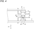
FIG. 4 is a partial side view of the base substrate and the extended substrate shown inFIG. 2 ; -
FIG. 5 is an electrical configuration diagram of the substrate unit having a high-grade specification shown inFIG. 1 ; -
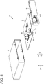
FIG. 6 is an exploded perspective view of a substrate unit having a standard specification according to the presently disclosed subject matter; and -
FIG. 7 is an electrical configuration diagram of the substrate unit having a standard specification shown inFIG. 6 . - A specific embodiment of the presently disclosed subject matter will be described below with reference to the drawings.
- By a method of manufacturing a substrate unit according to the present embodiment, a
substrate unit 1A (a second substrate unit) to be mounted on a vehicle having a high-grade specification (a second specification) and asubstrate unit 1B (a first substrate unit) to be mounted on a vehicle having a standard specification (a first specification) are manufactured. First, thesubstrate unit 1A having a high-grade specification will be described with reference toFIGS. 1 to 5 . - As shown in
FIG. 2 and the like, thesubstrate unit 1A having a high-grade specification includes abase substrate 2 for operating a standard electrical device (not shown), anextended substrate 3 for operating an extended electrical device (not shown), a connectingunit 4 for electrically connecting thebase substrate 2 and theextended substrate 3, and acase 5 for accommodating thebase substrate 2 and theextended substrate 3. The standard electrical device is an electrical device (for example, an air conditioner unit, a power window unit, or the like) that is attached in common to a vehicle having a high-grade specification and a vehicle having a standard specification. The extended electrical device is an electrical device that is selectively attached according to a specification of a vehicle. - As shown in
FIGS. 2 to 4 , a connector (a first connector) 21 and the like are mounted on thebase substrate 2. As shown inFIGS. 3 and4 , theconnector 21 includes terminals (first terminals) 22 and a housing (first housing) 23 that accommodates the terminals. In the present embodiment, as shown inFIG. 4 and the like, theterminal 22 is formed in a substantially L shape, one end thereof extending along a thickness direction D1 of thebase substrate 2 is connected to thebase substrate 2, and the other end thereof extending parallel to thebase substrate 2 is accommodated in thehousing 23. The other end of theterminal 22 is configured as, for example, a male terminal, and protrudes from thehousing 23. - The
housing 23 is provided withlocking projections 231 to be locked to ahousing 33 of an extendedconnector 31 to be described later. The locking projections 231 (first locking portions) are provided on outer surfaces of thehousing 23 facing in a direction orthogonal to both the thickness direction D1 and a direction along which the other end of theterminal 22 extends. Theconnector 21 is to be connected to an external connector (not shown) provided at an end of a wire harness. The wire harness is connected to a central ECU (host control device), a standard electrical device, and an extended electrical device (not shown). - As shown in
FIG. 5 , acontrol circuit 24, apower supply circuit 25, a communication interface (I/F) 26, and the like are mounted on thebase substrate 2. Thecontrol circuit 24 includes, for example, a microcomputer having a CPU. Thecontrol circuit 24 communicates with the central ECU and controls the standard electrical device and the extended electrical device according to instructions from the central ECU. Thepower supply circuit 25 generates power for thecontrol circuit 24 from power supplied via an external connector. The communication I/F 26 is a circuit that modulates and demodulates communication signals transmitted and received between the central ECU and thecontrol circuit 24. - Various circuits are mounted on the
base substrate 2 according to a type of the standard electrical device, and the various circuits are connected to thecontrol circuit 24. In the example shown inFIG. 5 , two input I/Fs 27 (input units) and three output drives (DRVs) 28 (output units) are mounted on thebase substrate 2. For example, when the standard electrical device is a device, that inputs ON/OFF information or the like to thecontrol circuit 24, such as a detection switch, the input I/F 27 is mounted with respect to the standard electrical device. Further, when the standard electrical device is a device, that operates based on an output from thecontrol circuit 24, such as a motor or a lamp, theoutput DRV 28 is mounted with respect to the standard electrical device. Thepower supply circuit 25, the communication I/F 26, the input I/Fs 27, and theoutput DRVs 28 are connected to theterminals 22, and when an external connector is connected to theterminals 22, thepower supply circuit 25, the communication I/F 26, the input I/Fs 27, and theoutput DRVs 28 are connected to the central ECU and/or the standard electrical device. - As shown in
FIGS. 2 to 4 , thebase substrate 2 and theextended substrate 3 are stacked along the thickness direction D1. An extended connector (a second connector) 31 and the like are mounted on theextended substrate 3. Theextended connector 31 includes terminals (second terminals) 32 and a housing (a second housing) 33 that accommodates theterminals 32. In the present embodiment, as shown inFIG. 4 , theterminal 32 is formed in a substantially L shape, one end thereof extending along the thickness direction D1 is connected to theextended substrate 3, and the other end thereof extending parallel to theextended substrate 3 is accommodated in thehousing 33. The other end of theterminal 32 is configured as, for example, a male terminal, and protrudes from thehousing 33. - The
housing 33 is provided with locking portions 331 (second locking portions) to be locked to thehousing 23 of theconnector 21. The lockingportions 331 are provided to protrude toward theconnector 21 and extend from outer surfaces of thehousing 33 facing in a direction orthogonal to both the thickness direction D1 and the other end of the terminal 32. Further, the lockingportion 331 is provided with alocking hole 332 into which the lockingprojection 231 is to be inserted. When thebase substrate 2 and theextended substrate 3 are stacked along the thickness direction D1 and thehousing 23 and thehousing 33 are disposed adjacently with each other along the thickness direction D1, the lockingprojections 231 are inserted into the locking holes 332, and thehousing 23 and thehousing 33 get locked. Therefore, thehousing 23 and thehousing 33 can be integrated with each other, and theconnector 21 and theextended connector 31 can together form one connector configured to be connected to an external connector. - Further, as shown in
FIG. 5 , various circuits are mounted on theextended substrate 3 according to a type of the extended electrical device, similarly to thebase substrate 2. In the example shown inFIG. 5 , three input I/Fs 34 (extended input units) and two output DRVs 35 (extended output units) are mounted. The input I/Fs 34 and theoutput DRVs 35 are connected to theterminals 32, and when an external connector is connected to theterminals 32, the input I/Fs 34 and theoutput DRVs 35 are connected to the extended electrical device. - In the present embodiment, as shown in
FIGS. 2 and3 , a pin header including a plurality ofterminals 41 extending orthogonal to thebase substrate 2 and theextended substrate 3 and aresin holder 42 for holding the plurality ofterminals 41 is used as the connectingunit 4. Both ends of each of theterminals 41 protrude from theholder 42. One end of each of theterminals 41 is connected to thebase substrate 2, and the other end of each of theterminals 41 is connected to theextended substrate 3. As shown inFIG. 5 , the input I/Fs 34 and theoutput DRVs 35 are connected to thecontrol circuit 24 via theterminals 41 of the connectingunit 4. - As shown in
FIG. 2 , thecase 5 includes a box-shaped casemain body 51 that is opened toward a front side, and afront cover 52 configured to close the front opening of the casemain body 51. Thefront cover 52 is provided with oneopening 521 through which an external connector is to be fitted. Thebase substrate 2 and theextended substrate 3 are accommodated into the casemain body 51 from the front opening of the casemain body 51. Thereafter, when the front opening of the casemain body 51 is closed by thefront cover 52, as shown inFIG. 1 , theterminals 22 and theterminals 32 are disposed to face theopening 521 and are exposed from the oneopening 521. Therefore, the external connector can be inserted through theopening 521 and connected to theconnectors 21 and theconnectors 31. - Next, the
substrate unit 1B having a standard specification will be described with reference toFIGS. 6 and7 . As shown inFIGS. 6 and7 , thesubstrate unit 1B having a standard specification includes thebase substrate 2 for operating a standard electrical device and acase 5 for accommodating thebase substrate 2, and does not include theextended substrate 3 and the connectingunit 4. Thebase substrate 2 and thecase 5 are the same as thebase substrate 2 and thecase 5 provided in thesubstrate unit 1A. When thebase substrate 2 is accommodated in thecase 5, theterminals 22 are disposed to face theopening 521 and are exposed from theopening 521. - Next, a method of manufacturing the
substrate units base substrate 2 on which theconnector 21 is mounted and theextended substrate 3 on which theextended connector 31 is mounted are prepared. As theextended substrate 3, a plurality of types of substrates having different numbers of input I/Fs 34 andoutput DRVs 35 may be prepared. In a case of a high-grade specification (a second specification), theextended substrate 3 corresponding to the specification is selected. Next, thebase substrate 2 and theextended substrate 3 are stacked, and thehousing 23 and thehousing 33 are locked. Further, thebase substrate 2 and theextended substrate 3 are connected to each other by using the connectingunit 4. Thereafter, thebase substrate 2 and theextended substrate 3 are accommodated in thecase 5 such that theterminals 22 and theterminals 32 face theopening 521 provided in thecase 5, and thesubstrate unit 1A is manufactured. - According to the
substrate unit 1A having a high-grade specification, theconnector 21 and theextended connector 31 are mounted on thebase substrate 2 and theextended substrate 3, respectively. Therefore, the input I/Fs 34 and theoutput DRVs 35 mounted on theextended substrate 3 do not have to be connected to theterminals 22 of theconnector 21 mounted on thebase substrate 2, so that the number of connections between thebase substrate 2 and theextended substrate 3 can be reduced. - Further, the
housing 23 of theconnector 21 mounted on thebase substrate 2 and thehousing 33 of theextended connector 31 mounted on theextended substrate 3 are locked to each other. Theterminals 22 and theterminals 32 are disposed to face theopening 521 provided in thecase 5. Therefore, theconnector 21 and theextended connector 31 can be coupled as one connector configured to be connected to an external connector, and the work of coupling theconnector 21 and theextended connector 31 respectively provided on thebase substrate 2 and theextended substrate 3 to the external connector can be reduced. - According to the
substrate unit 1A, thebase substrate 2 and theextended substrate 3 are stacked in the thickness direction D1, and thehousing 23 and thehousing 33 are disposed adjacently with each other in the thickness direction D1. Therefore, space saving can be achieved. - In a case of a standard specification (a first specification), the
substrate unit 1B is manufactured by accommodating only thebase substrate 2 in thecase 5 such that theterminals 22 face theopening 521 provided in thecase 5. According to thesubstrate unit 1B having a standard specification, the input I/Fs 34 and theoutput DRVs 35 that do not need to be used are not mounted on a vehicle having a standard specification. When the substrate is desired to be extended, thehousing 33 of theextended connector 31 mounted on theextended substrate 3 can be locked to the lockingprojections 231 of theconnector 21. - While the presently disclosed subject matter has been described with reference to certain exemplary embodiments thereof, the scope of the presently disclosed subject matter is not limited to the exemplary embodiments described above, and it will be understood by those skilled in the art that various changes and modifications may be made therein without departing from the scope of the presently disclosed subject matter as defined by the appended claims.
- According to the above-described embodiment, the
base substrate 2 and theextended substrate 3 are stacked along the thickness direction D1, but the presently disclosed subject matter is not limited thereto. Thebase substrate 2 and theextended substrate 3 may be disposed adjacently with each other along a width direction or a length direction of thebase substrate 2. - According to the above-described embodiment, the
base substrate 2 and theextended substrate 3 are electrically connected by the connectingunit 4, but the presently disclosed subject matter is not limited thereto. If theextended substrate 3 is provided with a control circuit, thebase substrate 2 and theextended substrate 3 may not be electrically connected to each other. - Further, according to the above-described embodiment, the
case 5 is used for both the standard specification and the high-grade specification, but the presently disclosed subject matter is not limited thereto. Acase 5 having asmall opening 521 may be used for the standard specification, and acase 5 having alarge opening 521 may be used for the high-grade specification. - According to an aspect of the embodiments described above, a substrate unit (1A) includes a first connector (21) including a first terminal (22) and a first housing (23) accommodating the first terminal (22), and configured to be connected to an external connector, a first substrate (2) on which the first connector (21) is mounted, a second connector (31) including a second terminal (32) and a second housing (33) accommodating the second terminal (32), and configured to be connected to the external connector, a second substrate (3) on which the second connector (31) is mounted and a case (5) accommodating the first substrate (2) and the second substrate (3). The first housing (23) is provided with a first locking portion (231). The second housing (33) is provided with a second locking portion (331). The first locking portion (231) and the second locking portion (331) are locked to each other. The first terminal (22) and the second terminal (32) are disposed to face an opening (521) provided in the case (5) through which the external connector is to be connected to the first connector (21) and the second connector (31).
- According to the substrate unit having the above configuration, the first locking portion of the first housing and the second locking portion of the second housing are locked to each other, and the first terminal and the second terminal are disposed to face the opening provided in the case for fitting the external connector. Therefore, the first connector and the second connector can be coupled as one connector to be connected to the external connector, and the work of coupling the first connector mounted on the first substrate, the second connector mounted on the second substrate, and the external connector can be reduced.
- The first substrate (2) and the second substrate (3) may be stacked on each other along a thickness direction (D1) of the substrate unit (1A), and the first housing (23) and the second housing (33) may be disposed adjacently with each other along the thickness direction (D1).
- With this configuration, since the first substrate and the second substrate can be stacked on each other in the thickness direction and accommodated in the case, space saving can be achieved.
- The substrate unit (1A) may further include a connecting unit (4) configured to connect the first substrate (2) and the second substrate (3) to each other. The first substrate (2) may include a control circuit (24) and an input unit (27) or an output unit (28) connected to the control circuit (24). The first terminal (22) may be connected to the input unit (27) or the output unit (28). The second substrate (3) may include an extended input unit (34) or an extended output unit (35). The second terminal (32) may be connected to the extended input unit (34) or the extended output unit (35). The control circuit (24) may be connected to the extended input unit (34) or the extended output unit (35) via the connecting unit (4).
- With this configuration, by connecting the first substrate and the second substrate, the extended input unit or the extended output unit can be connected to the control circuit. Thus, the input unit or the output unit can be extended.
- According to another aspect of the embodiments described above, a substrate unit (1B) includes a first connector (21) including a first terminal (22) and a first housing (23) accommodating the first terminal (22), and configured to be connected to an external connector, a first substrate (2) on which the first connector (21) is mounted and a case (5) accommodating the first substrate (2). The first housing (23) is provided with a first locking portion (231) configured to be locked to a second housing (33) of a second connector (31) mounted on a second substrate (3). The first terminal (22) is disposed to face an opening (521) provided in the case (5) through which the external connector is to be connected to the first connector (21).
- According to the substrate unit having the above configuration, when it is desired to extend the substrate, the second housing of the second connector mounted on the second substrate can be locked to the first locking portion of the first connector. Therefore, the first connector and the second connector can be coupled as one connector to be connected to the external connector, and the work of coupling the first connector provided on the first substrate, the second connector provided on the second substrate, and the external connector can be reduced.
- According to yet another aspect of the embodiments described above, a manufacturing method for manufacturing a substrate unit (1A, 1B), in which the substrate unit (1A, 1B) is either of a first substrate unit (1B) or a second substrate unit (1A), includes preparing a first substrate (2) on which a first connector (21) is mounted, the first connector (21) including a first terminal (22) and a first housing (23) accommodating the first terminal (22), the first housing (23) being provided with a first locking portion (231), the first connector (21) being configured to be connected to an external connector and a second substrate (3) on which a second connector (31) is mounted, the second connector (31) including a second terminal (32) and a second housing (33) accommodating the second terminal (32), the second housing (33) being provided with a second locking portion (331), the second connector (31) being configured to be connected to the external connector and manufacturing the first substrate unit (1B) or the second substrate unit (1A) selectively according to which of a first specification or a second specification is selected. When the first specification is selected, the first substrate unit (1B) is to be manufactured and the manufacturing of the first substrate unit (1B) includes accommodating only the first substrate (2) into the case (5) such that the first terminal (22) faces an opening (521) provided in the case (5) through which the external connector is to be connected to the first connector (21) and when the second specification is selected, the second substrate unit (1A) is to be manufactured and the manufacturing of the second substrate unit (1A) includes locking the first locking portion (231) and the second locking portion (331) with each other and accommodating both the first substrate (2) and the second substrate (3) into the case (5) such that the first terminal (22) and the second terminal (32) face the opening (521) provided in the case (5) through which the external connector is to be connected to the first connector (21) and the second connector (31).
- According to the method of manufacturing a substrate unit having the above configuration, in a case of a first specification, only the first substrate is accommodated in the case, and a substrate that is not used does not have to be accommodated in the case. In a case of a second specification, both the first substrate and the second substrate are accommodated in the case. At this time, the first housing of the first connector mounted on the first substrate and the second housing of the second connector mounted on the second substrate are locked to each other, and the first terminal and the second terminal are disposed to face the opening of the case. Therefore, the first connector and the second connector can be coupled as one connector which is to be connected to the external connector, and the work of coupling the first connector provided on the first substrate, the second connector provided on the second substrate, and the external connector can be reduced.
Claims (5)
- A substrate unit (1B) comprising:a first connector (21) including a first terminal (22) and a first housing (23) accommodating the first terminal (22), and configured to be connected to an external connector;a first substrate (2) on which the first connector (21) is mounted; anda case (5) accommodating the first substrate (2),wherein the first housing (23) is provided with a first locking portion (231) configured to be locked to a second housing (33) of a second connector (31) mounted on a second substrate (3), andwherein the first terminal (22) is disposed to face an opening (521) provided in the case (5) through which the external connector is to be connected to the first connector (21).
- A substrate unit (1A) comprising:the first connector (21) and the first substrate (2) according to claim 1;a second connector (31) including a second terminal (32) and a second housing (33) accommodating the second terminal (32), and configured to be connected to an external connector;a second substrate (3) on which the second connector (31) is mounted; anda case (5) accommodating the first substrate (2) and the second substrate (3),wherein the second housing (33) is provided with a second locking portion (331),wherein the first locking portion (231) and the second locking portion (331) are locked to each other, andwherein the first terminal (22) and the second terminal (32) are disposed to face an opening (521) provided in the case (5) through which the external connector is to be connected to the first connector (21) and the second connector (31).
- The substrate unit (1A) according to claim 2,wherein the first substrate (2) and the second substrate (3) are stacked on each other along a thickness direction (D1) of the substrate unit (1A), andwherein the first housing (23) and the second housing (33) are disposed adjacently with each other along the thickness direction (D1).
- The substrate unit (1A) according to claim 2 or 3 further including:a connecting unit (4) configured to connect the first substrate (2) and the second substrate (3) to each other,wherein the first substrate (2) includes a control circuit (24) and an input unit (27) or an output unit (28) connected to the control circuit (24),wherein the first terminal (22) is connected to the input unit (27) or the output unit (28),wherein the second substrate (3) includes an extended input unit (34) or an extended output unit (35),wherein the second terminal (32) is connected to the extended input unit (34) or the extended output unit (35), andwherein the control circuit (24) is connected to the extended input unit (34) or the extended output unit (35) via the connecting unit (4).
- A manufacturing method for manufacturing a substrate unit (1A, 1B), wherein the substrate unit (1A, 1B) is either of a first substrate unit (1B) or a second substrate unit (1A), the method including:preparinga first substrate (2) on which a first connector (21) is mounted, the first connector (21) including a first terminal (22) and a first housing (23) accommodating the first terminal (22), the first housing (23) being provided with a first locking portion (231), the first connector (21) being configured to be connected to an external connector, anda second substrate (3) on which a second connector (31) is mounted, the second connector (31) including a second terminal (32) and a second housing (33) accommodating the second terminal (32), the second housing (33) being provided with a second locking portion (331), the second connector (31) being configured to be connected to the external connector; andmanufacturing the first substrate unit (1B) or the second substrate unit (1A) selectively according to which of a first specification or a second specification is selected,wherein, when the first specification is selected, the first substrate unit (1B) is to be manufactured and the manufacturing of the first substrate unit (1B) includes: accommodating only the first substrate (2) into the case (5) such that the first terminal (22) faces an opening (521) provided in the case (5) through which the external connector is to be connected to the first connector (21); andwherein, when the second specification is selected, the second substrate unit (1A) is to be manufactured and the manufacturing of the second substrate unit (1A) includes: locking the first locking portion (231) and the second locking portion (331) with each other and accommodating both the first substrate (2) and the second substrate (3) into the case (5) such that the first terminal (22) and the second terminal (32) face the opening (521) provided in the case (5) through which the external connector is to be connected to the first connector (21) and the second connector (31).
Applications Claiming Priority (1)
| Application Number | Priority Date | Filing Date | Title |
|---|---|---|---|
| JP2021004953A JP7273077B2 (en) | 2021-01-15 | 2021-01-15 | Substrate unit and substrate unit manufacturing method |
Publications (2)
| Publication Number | Publication Date |
|---|---|
| EP4030876A1 true EP4030876A1 (en) | 2022-07-20 |
| EP4030876B1 EP4030876B1 (en) | 2024-02-14 |
Family
ID=79185609
Family Applications (1)
| Application Number | Title | Priority Date | Filing Date |
|---|---|---|---|
| EP21218123.4A Active EP4030876B1 (en) | 2021-01-15 | 2021-12-29 | Substrate unit and manufacturing method of substrate unit |
Country Status (4)
| Country | Link |
|---|---|
| US (1) | US11942712B2 (en) |
| EP (1) | EP4030876B1 (en) |
| JP (1) | JP7273077B2 (en) |
| CN (1) | CN114765919B (en) |
Families Citing this family (1)
| Publication number | Priority date | Publication date | Assignee | Title |
|---|---|---|---|---|
| JP7273077B2 (en) * | 2021-01-15 | 2023-05-12 | 矢崎総業株式会社 | Substrate unit and substrate unit manufacturing method |
Citations (3)
| Publication number | Priority date | Publication date | Assignee | Title |
|---|---|---|---|---|
| US5190461A (en) * | 1991-06-17 | 1993-03-02 | Fujitsu Limited | Connector assembly with both functions of coaxial connector and multiple contact connector |
| EP0746063A2 (en) * | 1995-05-31 | 1996-12-04 | Sumitomo Wiring Systems, Ltd. | Connector for a circuit board |
| JP2014187123A (en) | 2013-03-22 | 2014-10-02 | Mitsubishi Electric Corp | Electronic control device and manufacturing method of the same |
Family Cites Families (28)
| Publication number | Priority date | Publication date | Assignee | Title |
|---|---|---|---|---|
| JPH05343125A (en) * | 1992-06-04 | 1993-12-24 | Fujikura Ltd | Connector for printed board |
| DE19756345C2 (en) * | 1997-12-18 | 1999-12-30 | Telefunken Microelectron | Arrangement for contacting printed circuit boards |
| US6477593B1 (en) | 1998-06-11 | 2002-11-05 | Adaptec, Inc. | Stacked I/O bridge circuit assemblies having flexibly configurable connections |
| JP2002058134A (en) * | 2000-08-09 | 2002-02-22 | Auto Network Gijutsu Kenkyusho:Kk | Mounting structure of electronic control unit |
| JP2004055411A (en) * | 2002-07-23 | 2004-02-19 | Furukawa Electric Co Ltd:The | Electronic control unit |
| JP2005312132A (en) * | 2004-04-19 | 2005-11-04 | Auto Network Gijutsu Kenkyusho:Kk | Electrical junction box |
| KR101499950B1 (en) * | 2007-08-31 | 2015-03-09 | 엘지이노텍 주식회사 | Lighting device |
| JP4657329B2 (en) * | 2008-07-29 | 2011-03-23 | 日立オートモティブシステムズ株式会社 | Power converter and electric vehicle |
| US10321585B2 (en) * | 2008-07-29 | 2019-06-11 | Hitachi, Ltd. | Power conversion apparatus and electric vehicle |
| CN102611054A (en) * | 2011-01-24 | 2012-07-25 | 住友电装株式会社 | Electric connecting box |
| TWI456379B (en) * | 2012-07-23 | 2014-10-11 | Chicony Power Tech Co Ltd | Power system and its combined power supply unit |
| JP2015065395A (en) * | 2013-08-28 | 2015-04-09 | 矢崎総業株式会社 | Jumper module mounted circuit board and circuit board assembly |
| JP6274054B2 (en) * | 2014-09-10 | 2018-02-07 | 株式会社デンソー | Board connection structure |
| GB2530321B (en) * | 2014-09-19 | 2019-04-17 | Murata Manufacturing Co | Electronic device |
| JP5849166B1 (en) * | 2014-12-12 | 2016-01-27 | イリソ電子工業株式会社 | Board to board connection structure |
| JP6320332B2 (en) * | 2015-03-10 | 2018-05-09 | 東芝メモリ株式会社 | Electronics |
| JP6497213B2 (en) * | 2015-05-26 | 2019-04-10 | 株式会社デンソー | Power converter |
| JP2017182983A (en) * | 2016-03-29 | 2017-10-05 | 住友電装株式会社 | Connector, circuit structure, and electric connection box |
| CN107645231B (en) * | 2016-07-20 | 2019-10-11 | 光宝电子(广州)有限公司 | Power adapter |
| KR102530066B1 (en) * | 2017-12-08 | 2023-05-09 | 삼성전자주식회사 | Solid state drive apparatus |
| CN207783354U (en) | 2018-01-16 | 2018-08-28 | 台达电子工业股份有限公司 | expansion module of programmable controller |
| DE102018217659B4 (en) * | 2018-10-15 | 2022-08-04 | Vitesco Technologies GmbH | Arrangement and method for producing an electrically conductive connection between two substrates |
| KR20210031303A (en) * | 2019-09-11 | 2021-03-19 | 삼성전자주식회사 | An electronic device having a connector mounted on a circuit |
| JP2021064500A (en) * | 2019-10-11 | 2021-04-22 | 株式会社ジェイテクト | Substrate connection structure |
| KR102807004B1 (en) * | 2020-01-03 | 2025-05-14 | 삼성전자주식회사 | Electronic device including a structure for stacking substrates |
| US11309676B2 (en) * | 2020-05-12 | 2022-04-19 | Tactotek Oy | Integrated multilayer structure and a method for manufacturing a multilayer structure |
| JP7273077B2 (en) * | 2021-01-15 | 2023-05-12 | 矢崎総業株式会社 | Substrate unit and substrate unit manufacturing method |
| KR102467844B1 (en) * | 2021-04-21 | 2022-11-16 | 삼성전자주식회사 | Solid state drive apparatus and data storage apparatus including the same |
-
2021
- 2021-01-15 JP JP2021004953A patent/JP7273077B2/en active Active
- 2021-12-20 CN CN202111559676.0A patent/CN114765919B/en active Active
- 2021-12-22 US US17/558,593 patent/US11942712B2/en active Active
- 2021-12-29 EP EP21218123.4A patent/EP4030876B1/en active Active
Patent Citations (3)
| Publication number | Priority date | Publication date | Assignee | Title |
|---|---|---|---|---|
| US5190461A (en) * | 1991-06-17 | 1993-03-02 | Fujitsu Limited | Connector assembly with both functions of coaxial connector and multiple contact connector |
| EP0746063A2 (en) * | 1995-05-31 | 1996-12-04 | Sumitomo Wiring Systems, Ltd. | Connector for a circuit board |
| JP2014187123A (en) | 2013-03-22 | 2014-10-02 | Mitsubishi Electric Corp | Electronic control device and manufacturing method of the same |
Non-Patent Citations (1)
| Title |
|---|
| ADAMS G L: "CONNECTORS FOR USE WITH MULTIPLE PCBS", MOTOROLA TECHNICAL DEVELOPMENTS, MOTOROLA INC. SCHAUMBURG, ILLINOIS, US, vol. 11, 1 October 1990 (1990-10-01), pages 43 - 45, XP000178615, ISSN: 0887-5286 * |
Also Published As
| Publication number | Publication date |
|---|---|
| JP7273077B2 (en) | 2023-05-12 |
| JP2022109562A (en) | 2022-07-28 |
| CN114765919B (en) | 2024-05-28 |
| CN114765919A (en) | 2022-07-19 |
| US11942712B2 (en) | 2024-03-26 |
| EP4030876B1 (en) | 2024-02-14 |
| US20220231438A1 (en) | 2022-07-21 |
Similar Documents
| Publication | Publication Date | Title |
|---|---|---|
| US4689718A (en) | Programmable junction box | |
| EP1096608B1 (en) | Sensor system and connector used therefor | |
| US11942712B2 (en) | Substrate unit and manufacturing method of substrate unit | |
| CN100438720C (en) | Integrated electrical module architecture for vehicles | |
| US8784132B2 (en) | Electrical connector assembly having connector shroud | |
| TWI287335B (en) | Relay connection circuit and relay connector | |
| CN100454679C (en) | Incorrect connection judgment method and electronic equipment | |
| US6106307A (en) | Pluggable I/O breakout connector module | |
| US7525221B2 (en) | Connection arrangement for connecting an electronic component and a power circuit of a control device | |
| KR102741476B1 (en) | Compatible connector for a vehicle | |
| CN223260882U (en) | Board end connector | |
| CN220368192U (en) | Wire end straight end connector | |
| JP7572410B2 (en) | Connector device | |
| CN222813968U (en) | Electric connection structure | |
| KR100451925B1 (en) | Integrated Circuit Module | |
| CN210379666U (en) | Connector socket and controller | |
| CN216528661U (en) | Circuit breaker and power utilization system | |
| KR20190137024A (en) | Two-way joint connector | |
| CN213413701U (en) | Automobile adapter | |
| EP4451478A1 (en) | Connector module and electronic device | |
| US20250215897A1 (en) | Apparatus and system for integrated fluid pumps | |
| US5997313A (en) | Retrofit/interface adapter | |
| KR102077015B1 (en) | Two-way joint connector | |
| EP2182643A2 (en) | Modular modem | |
| JPH0211813Y2 (en) |
Legal Events
| Date | Code | Title | Description |
|---|---|---|---|
| PUAI | Public reference made under article 153(3) epc to a published international application that has entered the european phase |
Free format text: ORIGINAL CODE: 0009012 |
|
| STAA | Information on the status of an ep patent application or granted ep patent |
Free format text: STATUS: REQUEST FOR EXAMINATION WAS MADE |
|
| 17P | Request for examination filed |
Effective date: 20211229 |
|
| AK | Designated contracting states |
Kind code of ref document: A1 Designated state(s): AL AT BE BG CH CY CZ DE DK EE ES FI FR GB GR HR HU IE IS IT LI LT LU LV MC MK MT NL NO PL PT RO RS SE SI SK SM TR |
|
| STAA | Information on the status of an ep patent application or granted ep patent |
Free format text: STATUS: EXAMINATION IS IN PROGRESS |
|
| 17Q | First examination report despatched |
Effective date: 20221103 |
|
| RAP3 | Party data changed (applicant data changed or rights of an application transferred) |
Owner name: YAZAKI CORPORATION |
|
| GRAP | Despatch of communication of intention to grant a patent |
Free format text: ORIGINAL CODE: EPIDOSNIGR1 |
|
| STAA | Information on the status of an ep patent application or granted ep patent |
Free format text: STATUS: GRANT OF PATENT IS INTENDED |
|
| INTG | Intention to grant announced |
Effective date: 20231124 |
|
| GRAS | Grant fee paid |
Free format text: ORIGINAL CODE: EPIDOSNIGR3 |
|
| GRAA | (expected) grant |
Free format text: ORIGINAL CODE: 0009210 |
|
| STAA | Information on the status of an ep patent application or granted ep patent |
Free format text: STATUS: THE PATENT HAS BEEN GRANTED |
|
| AK | Designated contracting states |
Kind code of ref document: B1 Designated state(s): AL AT BE BG CH CY CZ DE DK EE ES FI FR GB GR HR HU IE IS IT LI LT LU LV MC MK MT NL NO PL PT RO RS SE SI SK SM TR |
|
| REG | Reference to a national code |
Ref country code: GB Ref legal event code: FG4D |
|
| REG | Reference to a national code |
Ref country code: CH Ref legal event code: EP |
|
| REG | Reference to a national code |
Ref country code: DE Ref legal event code: R096 Ref document number: 602021009371 Country of ref document: DE |
|
| REG | Reference to a national code |
Ref country code: IE Ref legal event code: FG4D |
|
| REG | Reference to a national code |
Ref country code: LT Ref legal event code: MG9D |
|
| REG | Reference to a national code |
Ref country code: NL Ref legal event code: MP Effective date: 20240214 |
|
| PG25 | Lapsed in a contracting state [announced via postgrant information from national office to epo] |
Ref country code: IS Free format text: LAPSE BECAUSE OF FAILURE TO SUBMIT A TRANSLATION OF THE DESCRIPTION OR TO PAY THE FEE WITHIN THE PRESCRIBED TIME-LIMIT Effective date: 20240614 |
|
| PG25 | Lapsed in a contracting state [announced via postgrant information from national office to epo] |
Ref country code: LT Free format text: LAPSE BECAUSE OF FAILURE TO SUBMIT A TRANSLATION OF THE DESCRIPTION OR TO PAY THE FEE WITHIN THE PRESCRIBED TIME-LIMIT Effective date: 20240214 |
|
| PG25 | Lapsed in a contracting state [announced via postgrant information from national office to epo] |
Ref country code: GR Free format text: LAPSE BECAUSE OF FAILURE TO SUBMIT A TRANSLATION OF THE DESCRIPTION OR TO PAY THE FEE WITHIN THE PRESCRIBED TIME-LIMIT Effective date: 20240515 |
|
| REG | Reference to a national code |
Ref country code: AT Ref legal event code: MK05 Ref document number: 1658191 Country of ref document: AT Kind code of ref document: T Effective date: 20240214 |
|
| PG25 | Lapsed in a contracting state [announced via postgrant information from national office to epo] |
Ref country code: HR Free format text: LAPSE BECAUSE OF FAILURE TO SUBMIT A TRANSLATION OF THE DESCRIPTION OR TO PAY THE FEE WITHIN THE PRESCRIBED TIME-LIMIT Effective date: 20240214 Ref country code: RS Free format text: LAPSE BECAUSE OF FAILURE TO SUBMIT A TRANSLATION OF THE DESCRIPTION OR TO PAY THE FEE WITHIN THE PRESCRIBED TIME-LIMIT Effective date: 20240514 Ref country code: NL Free format text: LAPSE BECAUSE OF FAILURE TO SUBMIT A TRANSLATION OF THE DESCRIPTION OR TO PAY THE FEE WITHIN THE PRESCRIBED TIME-LIMIT Effective date: 20240214 |
|
| PG25 | Lapsed in a contracting state [announced via postgrant information from national office to epo] |
Ref country code: ES Free format text: LAPSE BECAUSE OF FAILURE TO SUBMIT A TRANSLATION OF THE DESCRIPTION OR TO PAY THE FEE WITHIN THE PRESCRIBED TIME-LIMIT Effective date: 20240214 |
|
| PG25 | Lapsed in a contracting state [announced via postgrant information from national office to epo] |
Ref country code: AT Free format text: LAPSE BECAUSE OF FAILURE TO SUBMIT A TRANSLATION OF THE DESCRIPTION OR TO PAY THE FEE WITHIN THE PRESCRIBED TIME-LIMIT Effective date: 20240214 |
|
| PG25 | Lapsed in a contracting state [announced via postgrant information from national office to epo] |
Ref country code: RS Free format text: LAPSE BECAUSE OF FAILURE TO SUBMIT A TRANSLATION OF THE DESCRIPTION OR TO PAY THE FEE WITHIN THE PRESCRIBED TIME-LIMIT Effective date: 20240514 Ref country code: NO Free format text: LAPSE BECAUSE OF FAILURE TO SUBMIT A TRANSLATION OF THE DESCRIPTION OR TO PAY THE FEE WITHIN THE PRESCRIBED TIME-LIMIT Effective date: 20240514 Ref country code: NL Free format text: LAPSE BECAUSE OF FAILURE TO SUBMIT A TRANSLATION OF THE DESCRIPTION OR TO PAY THE FEE WITHIN THE PRESCRIBED TIME-LIMIT Effective date: 20240214 Ref country code: LT Free format text: LAPSE BECAUSE OF FAILURE TO SUBMIT A TRANSLATION OF THE DESCRIPTION OR TO PAY THE FEE WITHIN THE PRESCRIBED TIME-LIMIT Effective date: 20240214 Ref country code: IS Free format text: LAPSE BECAUSE OF FAILURE TO SUBMIT A TRANSLATION OF THE DESCRIPTION OR TO PAY THE FEE WITHIN THE PRESCRIBED TIME-LIMIT Effective date: 20240614 Ref country code: HR Free format text: LAPSE BECAUSE OF FAILURE TO SUBMIT A TRANSLATION OF THE DESCRIPTION OR TO PAY THE FEE WITHIN THE PRESCRIBED TIME-LIMIT Effective date: 20240214 Ref country code: GR Free format text: LAPSE BECAUSE OF FAILURE TO SUBMIT A TRANSLATION OF THE DESCRIPTION OR TO PAY THE FEE WITHIN THE PRESCRIBED TIME-LIMIT Effective date: 20240515 Ref country code: FI Free format text: LAPSE BECAUSE OF FAILURE TO SUBMIT A TRANSLATION OF THE DESCRIPTION OR TO PAY THE FEE WITHIN THE PRESCRIBED TIME-LIMIT Effective date: 20240214 Ref country code: ES Free format text: LAPSE BECAUSE OF FAILURE TO SUBMIT A TRANSLATION OF THE DESCRIPTION OR TO PAY THE FEE WITHIN THE PRESCRIBED TIME-LIMIT Effective date: 20240214 Ref country code: BG Free format text: LAPSE BECAUSE OF FAILURE TO SUBMIT A TRANSLATION OF THE DESCRIPTION OR TO PAY THE FEE WITHIN THE PRESCRIBED TIME-LIMIT Effective date: 20240214 Ref country code: AT Free format text: LAPSE BECAUSE OF FAILURE TO SUBMIT A TRANSLATION OF THE DESCRIPTION OR TO PAY THE FEE WITHIN THE PRESCRIBED TIME-LIMIT Effective date: 20240214 |
|
| PG25 | Lapsed in a contracting state [announced via postgrant information from national office to epo] |
Ref country code: PL Free format text: LAPSE BECAUSE OF FAILURE TO SUBMIT A TRANSLATION OF THE DESCRIPTION OR TO PAY THE FEE WITHIN THE PRESCRIBED TIME-LIMIT Effective date: 20240214 Ref country code: PT Free format text: LAPSE BECAUSE OF FAILURE TO SUBMIT A TRANSLATION OF THE DESCRIPTION OR TO PAY THE FEE WITHIN THE PRESCRIBED TIME-LIMIT Effective date: 20240614 |
|
| PG25 | Lapsed in a contracting state [announced via postgrant information from national office to epo] |
Ref country code: SE Free format text: LAPSE BECAUSE OF FAILURE TO SUBMIT A TRANSLATION OF THE DESCRIPTION OR TO PAY THE FEE WITHIN THE PRESCRIBED TIME-LIMIT Effective date: 20240214 Ref country code: PT Free format text: LAPSE BECAUSE OF FAILURE TO SUBMIT A TRANSLATION OF THE DESCRIPTION OR TO PAY THE FEE WITHIN THE PRESCRIBED TIME-LIMIT Effective date: 20240614 Ref country code: PL Free format text: LAPSE BECAUSE OF FAILURE TO SUBMIT A TRANSLATION OF THE DESCRIPTION OR TO PAY THE FEE WITHIN THE PRESCRIBED TIME-LIMIT Effective date: 20240214 Ref country code: LV Free format text: LAPSE BECAUSE OF FAILURE TO SUBMIT A TRANSLATION OF THE DESCRIPTION OR TO PAY THE FEE WITHIN THE PRESCRIBED TIME-LIMIT Effective date: 20240214 |
|
| PG25 | Lapsed in a contracting state [announced via postgrant information from national office to epo] |
Ref country code: DK Free format text: LAPSE BECAUSE OF FAILURE TO SUBMIT A TRANSLATION OF THE DESCRIPTION OR TO PAY THE FEE WITHIN THE PRESCRIBED TIME-LIMIT Effective date: 20240214 |
|
| PG25 | Lapsed in a contracting state [announced via postgrant information from national office to epo] |
Ref country code: SM Free format text: LAPSE BECAUSE OF FAILURE TO SUBMIT A TRANSLATION OF THE DESCRIPTION OR TO PAY THE FEE WITHIN THE PRESCRIBED TIME-LIMIT Effective date: 20240214 |
|
| PG25 | Lapsed in a contracting state [announced via postgrant information from national office to epo] |
Ref country code: CZ Free format text: LAPSE BECAUSE OF FAILURE TO SUBMIT A TRANSLATION OF THE DESCRIPTION OR TO PAY THE FEE WITHIN THE PRESCRIBED TIME-LIMIT Effective date: 20240214 Ref country code: EE Free format text: LAPSE BECAUSE OF FAILURE TO SUBMIT A TRANSLATION OF THE DESCRIPTION OR TO PAY THE FEE WITHIN THE PRESCRIBED TIME-LIMIT Effective date: 20240214 |
|
| PG25 | Lapsed in a contracting state [announced via postgrant information from national office to epo] |
Ref country code: SK Free format text: LAPSE BECAUSE OF FAILURE TO SUBMIT A TRANSLATION OF THE DESCRIPTION OR TO PAY THE FEE WITHIN THE PRESCRIBED TIME-LIMIT Effective date: 20240214 |
|
| PG25 | Lapsed in a contracting state [announced via postgrant information from national office to epo] |
Ref country code: SM Free format text: LAPSE BECAUSE OF FAILURE TO SUBMIT A TRANSLATION OF THE DESCRIPTION OR TO PAY THE FEE WITHIN THE PRESCRIBED TIME-LIMIT Effective date: 20240214 Ref country code: SK Free format text: LAPSE BECAUSE OF FAILURE TO SUBMIT A TRANSLATION OF THE DESCRIPTION OR TO PAY THE FEE WITHIN THE PRESCRIBED TIME-LIMIT Effective date: 20240214 Ref country code: RO Free format text: LAPSE BECAUSE OF FAILURE TO SUBMIT A TRANSLATION OF THE DESCRIPTION OR TO PAY THE FEE WITHIN THE PRESCRIBED TIME-LIMIT Effective date: 20240214 Ref country code: EE Free format text: LAPSE BECAUSE OF FAILURE TO SUBMIT A TRANSLATION OF THE DESCRIPTION OR TO PAY THE FEE WITHIN THE PRESCRIBED TIME-LIMIT Effective date: 20240214 Ref country code: DK Free format text: LAPSE BECAUSE OF FAILURE TO SUBMIT A TRANSLATION OF THE DESCRIPTION OR TO PAY THE FEE WITHIN THE PRESCRIBED TIME-LIMIT Effective date: 20240214 Ref country code: CZ Free format text: LAPSE BECAUSE OF FAILURE TO SUBMIT A TRANSLATION OF THE DESCRIPTION OR TO PAY THE FEE WITHIN THE PRESCRIBED TIME-LIMIT Effective date: 20240214 |
|
| REG | Reference to a national code |
Ref country code: DE Ref legal event code: R097 Ref document number: 602021009371 Country of ref document: DE |
|
| PG25 | Lapsed in a contracting state [announced via postgrant information from national office to epo] |
Ref country code: IT Free format text: LAPSE BECAUSE OF FAILURE TO SUBMIT A TRANSLATION OF THE DESCRIPTION OR TO PAY THE FEE WITHIN THE PRESCRIBED TIME-LIMIT Effective date: 20240214 |
|
| PLBE | No opposition filed within time limit |
Free format text: ORIGINAL CODE: 0009261 |
|
| STAA | Information on the status of an ep patent application or granted ep patent |
Free format text: STATUS: NO OPPOSITION FILED WITHIN TIME LIMIT |
|
| PG25 | Lapsed in a contracting state [announced via postgrant information from national office to epo] |
Ref country code: IT Free format text: LAPSE BECAUSE OF FAILURE TO SUBMIT A TRANSLATION OF THE DESCRIPTION OR TO PAY THE FEE WITHIN THE PRESCRIBED TIME-LIMIT Effective date: 20240214 |
|
| 26N | No opposition filed |
Effective date: 20241115 |
|
| PG25 | Lapsed in a contracting state [announced via postgrant information from national office to epo] |
Ref country code: SI Free format text: LAPSE BECAUSE OF FAILURE TO SUBMIT A TRANSLATION OF THE DESCRIPTION OR TO PAY THE FEE WITHIN THE PRESCRIBED TIME-LIMIT Effective date: 20240214 |
|
| PG25 | Lapsed in a contracting state [announced via postgrant information from national office to epo] |
Ref country code: MC Free format text: LAPSE BECAUSE OF FAILURE TO SUBMIT A TRANSLATION OF THE DESCRIPTION OR TO PAY THE FEE WITHIN THE PRESCRIBED TIME-LIMIT Effective date: 20240214 |
|
| REG | Reference to a national code |
Ref country code: CH Ref legal event code: PL |
|
| PG25 | Lapsed in a contracting state [announced via postgrant information from national office to epo] |
Ref country code: LU Free format text: LAPSE BECAUSE OF NON-PAYMENT OF DUE FEES Effective date: 20241229 |
|
| REG | Reference to a national code |
Ref country code: BE Ref legal event code: MM Effective date: 20241231 |
|
| PG25 | Lapsed in a contracting state [announced via postgrant information from national office to epo] |
Ref country code: BE Free format text: LAPSE BECAUSE OF NON-PAYMENT OF DUE FEES Effective date: 20241231 |
|
| PG25 | Lapsed in a contracting state [announced via postgrant information from national office to epo] |
Ref country code: FR Free format text: LAPSE BECAUSE OF NON-PAYMENT OF DUE FEES Effective date: 20241231 |
|
| PG25 | Lapsed in a contracting state [announced via postgrant information from national office to epo] |
Ref country code: CH Free format text: LAPSE BECAUSE OF NON-PAYMENT OF DUE FEES Effective date: 20241231 |
|
| PG25 | Lapsed in a contracting state [announced via postgrant information from national office to epo] |
Ref country code: IE Free format text: LAPSE BECAUSE OF NON-PAYMENT OF DUE FEES Effective date: 20241229 |
|
| PGFP | Annual fee paid to national office [announced via postgrant information from national office to epo] |
Ref country code: DE Payment date: 20251104 Year of fee payment: 5 |
|
| PG25 | Lapsed in a contracting state [announced via postgrant information from national office to epo] |
Ref country code: CY Free format text: LAPSE BECAUSE OF FAILURE TO SUBMIT A TRANSLATION OF THE DESCRIPTION OR TO PAY THE FEE WITHIN THE PRESCRIBED TIME-LIMIT Effective date: 20240214 |