EP4030700B1 - Method for allocating communication id and system providing the method - Google Patents
Method for allocating communication id and system providing the method Download PDFInfo
- Publication number
- EP4030700B1 EP4030700B1 EP21876736.6A EP21876736A EP4030700B1 EP 4030700 B1 EP4030700 B1 EP 4030700B1 EP 21876736 A EP21876736 A EP 21876736A EP 4030700 B1 EP4030700 B1 EP 4030700B1
- Authority
- EP
- European Patent Office
- Prior art keywords
- slave
- communication
- current amount
- bms
- bmss
- Prior art date
- Legal status (The legal status is an assumption and is not a legal conclusion. Google has not performed a legal analysis and makes no representation as to the accuracy of the status listed.)
- Active
Links
Images



Classifications
-
- H—ELECTRICITY
- H04—ELECTRIC COMMUNICATION TECHNIQUE
- H04L—TRANSMISSION OF DIGITAL INFORMATION, e.g. TELEGRAPHIC COMMUNICATION
- H04L61/00—Network arrangements, protocols or services for addressing or naming
- H04L61/50—Address allocation
- H04L61/5092—Address allocation by self-assignment, e.g. picking addresses at random and testing if they are already in use
-
- G—PHYSICS
- G01—MEASURING; TESTING
- G01R—MEASURING ELECTRIC VARIABLES; MEASURING MAGNETIC VARIABLES
- G01R1/00—Details of instruments or arrangements of the types included in groups G01R5/00 - G01R13/00 and G01R31/00
- G01R1/20—Modifications of basic electric elements for use in electric measuring instruments; Structural combinations of such elements with such instruments
- G01R1/203—Resistors used for electric measuring, e.g. decade resistors standards, resistors for comparators, series resistors, shunts
-
- G—PHYSICS
- G01—MEASURING; TESTING
- G01R—MEASURING ELECTRIC VARIABLES; MEASURING MAGNETIC VARIABLES
- G01R19/00—Arrangements for measuring currents or voltages or for indicating presence or sign thereof
- G01R19/10—Measuring sum, difference or ratio
-
- H—ELECTRICITY
- H01—ELECTRIC ELEMENTS
- H01M—PROCESSES OR MEANS, e.g. BATTERIES, FOR THE DIRECT CONVERSION OF CHEMICAL ENERGY INTO ELECTRICAL ENERGY
- H01M10/00—Secondary cells; Manufacture thereof
- H01M10/42—Methods or arrangements for servicing or maintenance of secondary cells or secondary half-cells
- H01M10/4207—Methods or arrangements for servicing or maintenance of secondary cells or secondary half-cells for several batteries or cells simultaneously or sequentially
-
- H—ELECTRICITY
- H01—ELECTRIC ELEMENTS
- H01M—PROCESSES OR MEANS, e.g. BATTERIES, FOR THE DIRECT CONVERSION OF CHEMICAL ENERGY INTO ELECTRICAL ENERGY
- H01M10/00—Secondary cells; Manufacture thereof
- H01M10/42—Methods or arrangements for servicing or maintenance of secondary cells or secondary half-cells
- H01M10/425—Structural combination with electronic components, e.g. electronic circuits integrated to the outside of the casing
-
- H—ELECTRICITY
- H02—GENERATION; CONVERSION OR DISTRIBUTION OF ELECTRIC POWER
- H02J—ELECTRIC POWER NETWORKS; CIRCUIT ARRANGEMENTS OR SYSTEMS FOR SUPPLYING OR DISTRIBUTING ELECTRIC POWER; SYSTEMS FOR STORING ELECTRIC ENERGY
- H02J7/00—Circuit arrangements for charging or discharging batteries or for supplying loads from batteries
- H02J7/40—Circuit arrangements for charging or discharging batteries or for supplying loads from batteries characterised by the exchange of charge or discharge related data
-
- H—ELECTRICITY
- H04—ELECTRIC COMMUNICATION TECHNIQUE
- H04L—TRANSMISSION OF DIGITAL INFORMATION, e.g. TELEGRAPHIC COMMUNICATION
- H04L12/00—Data switching networks
- H04L12/28—Data switching networks characterised by path configuration, e.g. LAN [Local Area Networks] or WAN [Wide Area Networks]
- H04L12/40—Bus networks
- H04L12/40006—Architecture of a communication node
- H04L12/40032—Details regarding a bus interface enhancer
-
- H—ELECTRICITY
- H04—ELECTRIC COMMUNICATION TECHNIQUE
- H04L—TRANSMISSION OF DIGITAL INFORMATION, e.g. TELEGRAPHIC COMMUNICATION
- H04L12/00—Data switching networks
- H04L12/28—Data switching networks characterised by path configuration, e.g. LAN [Local Area Networks] or WAN [Wide Area Networks]
- H04L12/40—Bus networks
- H04L12/40006—Architecture of a communication node
- H04L12/40039—Details regarding the setting of the power status of a node according to activity on the bus
-
- H—ELECTRICITY
- H04—ELECTRIC COMMUNICATION TECHNIQUE
- H04L—TRANSMISSION OF DIGITAL INFORMATION, e.g. TELEGRAPHIC COMMUNICATION
- H04L12/00—Data switching networks
- H04L12/28—Data switching networks characterised by path configuration, e.g. LAN [Local Area Networks] or WAN [Wide Area Networks]
- H04L12/40—Bus networks
- H04L12/40006—Architecture of a communication node
- H04L12/40045—Details regarding the feeding of energy to the node from the bus
-
- H—ELECTRICITY
- H04—ELECTRIC COMMUNICATION TECHNIQUE
- H04L—TRANSMISSION OF DIGITAL INFORMATION, e.g. TELEGRAPHIC COMMUNICATION
- H04L61/00—Network arrangements, protocols or services for addressing or naming
- H04L61/30—Managing network names, e.g. use of aliases or nicknames
- H04L61/3015—Name registration, generation or assignment
-
- H—ELECTRICITY
- H01—ELECTRIC ELEMENTS
- H01M—PROCESSES OR MEANS, e.g. BATTERIES, FOR THE DIRECT CONVERSION OF CHEMICAL ENERGY INTO ELECTRICAL ENERGY
- H01M10/00—Secondary cells; Manufacture thereof
- H01M10/42—Methods or arrangements for servicing or maintenance of secondary cells or secondary half-cells
- H01M10/425—Structural combination with electronic components, e.g. electronic circuits integrated to the outside of the casing
- H01M2010/4278—Systems for data transfer from batteries, e.g. transfer of battery parameters to a controller, data transferred between battery controller and main controller
-
- H—ELECTRICITY
- H04—ELECTRIC COMMUNICATION TECHNIQUE
- H04L—TRANSMISSION OF DIGITAL INFORMATION, e.g. TELEGRAPHIC COMMUNICATION
- H04L12/00—Data switching networks
- H04L12/28—Data switching networks characterised by path configuration, e.g. LAN [Local Area Networks] or WAN [Wide Area Networks]
- H04L12/40—Bus networks
- H04L2012/40208—Bus networks characterized by the use of a particular bus standard
- H04L2012/40215—Controller Area Network CAN
Definitions
- Electric vehicles such as hybrid vehicles (HV), plug-in hybrid electric vehicles (PHEV), or battery electric vehicles (BEV) may be driven with a high voltage battery.
- a battery system may include a battery pack configured by connecting a plurality of battery modules in series or in parallel, and the battery pack may include a battery management system (BMS).
- BMS battery management system
- the first current amounts applied to the respective third to fifth slave BMSs 200_2 to 200_5 through the second to fifth input ends may be calculated to be 180 mA, 120 mA, and 60 mA as shown in FIG. 4 .
- the respective second to fifth slave BMSs 200_2 to 200_5 may automatically allocate the communication IDs (ID_2, ID_3, ID_4, and ID_5) that correspond to the calculated first current amounts of 240 mA, 180 mA, 120 mA, and 60 mA as the communication IDs of the second to fifth slave BMSs 200_2 to 200_5 based on the communication ID allocating table.
- the second slave BMS 200_2 may automatically allocate the second communication ID (ID_2) as the communication ID of the second slave BMS 200_2.
- the third slave BMS 200_3 to fifth slave BMS 200_5 may automatically allocate the third communication ID (ID_3), the fourth communication ID (ID_4), and the fifth communication ID (ID_5) as the communication IDs of the third slave BMS 200_3 to the fifth slave BMS 200_5.
- FIG. 6 shows a flowchart of a method for allocating communication IDs according to an embodiment.
- the master BMS 100 may broadcast a signal for instructing allocation of communication IDs through the network in the case of the first connection to the slave BMSs 200_1 to 200_N (S100).
- the master BMS 100 may not specify the respective slave BMSs 200_1 to 200_N and may not transmit signals before the communication IDs are allocated, so it may broadcast the communication ID allocating instruction to the slave BMSs 200_1 to 200_N through the network.
- the master BMS 100 may broadcast the signal for instructing allocation of communication IDs when power is supplied from the power source through a power line.
- the slave BMS 200 may allocate a predetermined communication ID as the communication ID of the slave BMS 200 based on the first current amount applied through the power line (S200).
- the slave BMSs 200_1 to 200_N are sequentially connected to the power line for supplying power.
- the slave BMSs 200_1 to 200_N may output the second current amount that is the first current amount minus the consumed current amount for driving through the power line.
- the first current amount may correspond to the summation value of the consumed current amount of the slave BMS 200 receiving the first current amount and the consumed current amount of at least one posterior slave BMS 200 sequentially connected to the slave BMS 200 receiving the first current amount.
- the slave BMS 200 may measure the voltages at the front end and the rear end of the shunt resistor R1 coupled in series to the power line and may calculate the voltage value caused by the voltage drop (S210).
- the slave BMS 200 may calculate the first current amount based on the voltage value caused by the voltage drop ( ⁇ ) of the shunt resistor R1 and the resistance of the shunt resistor R1 (S230).
- the resistance of the shunt resistor R1 may be stored in the slave storage unit 230.
- the second to fifth slave BMSs 200_2 to 200_5 may respectively calculate the first current amounts.
- the first current amounts of the second to fifth slave BMS 200_2 to 200_N may be 240 mA, 180 mA, 120 mA, and 60 mA.
- the slave BMS 200 may allocate the communication ID that corresponds to the first current amount as the communication ID of the slave BMS 200 based on the communication ID allocating table (S250).
- the communication ID allocating table may include a plurality of communication IDs that correspond to a plurality of first current amounts (11 to I5).
- the master BMS 100 may receive the calculated first current amounts and the allocated communication IDs from the slave BMSs 200_1 to 200_N, and may verify the allocated communication IDs (S300).
- the master BMS 100 may receive the first current amount of 330 mA and the second communication ID (ID_2) from the second slave BMS 200_2, and may compare them with the communication ID allocating table to verify the second communication ID.
- the first current amount corresponding to the second communication ID (ID_2) is 240 mA. This is different from the first current amount 330 mA and the communication ID (ID_2) received from the second slave BMS 200_2.
- the master BMS 100 may determine the allocation of communication IDs performed by the second slave BMS 200_2 to have errors.
- the master BMS 100 may broadcast an instruction for instructing allocation of communication IDs to the slave BMSs 200_1 to 200_N.
Landscapes
- Engineering & Computer Science (AREA)
- Signal Processing (AREA)
- Computer Networks & Wireless Communication (AREA)
- General Chemical & Material Sciences (AREA)
- Manufacturing & Machinery (AREA)
- Chemical & Material Sciences (AREA)
- Chemical Kinetics & Catalysis (AREA)
- Electrochemistry (AREA)
- Physics & Mathematics (AREA)
- General Physics & Mathematics (AREA)
- Microelectronics & Electronic Packaging (AREA)
- Power Engineering (AREA)
- Cable Transmission Systems, Equalization Of Radio And Reduction Of Echo (AREA)
- Remote Monitoring And Control Of Power-Distribution Networks (AREA)
- Charge And Discharge Circuits For Batteries Or The Like (AREA)
- Mobile Radio Communication Systems (AREA)
Description
- The present invention relates to a method for allocating a communication ID for communication between a master battery management system (BMS) and a plurality of slave BMSs, and a system for providing the method.
- Electric vehicles (EV), such as hybrid vehicles (HV), plug-in hybrid electric vehicles (PHEV), or battery electric vehicles (BEV), may be driven with a high voltage battery. To provide high-voltage power, a battery system may include a battery pack configured by connecting a plurality of battery modules in series or in parallel, and the battery pack may include a battery management system (BMS).
- The battery management system (BMS) may include a plurality of slave BMSs for monitoring and managing a plurality of battery modules, and a master BMS for managing the slave BMS in an integrated way. The slave BMSs may transmit battery data including a battery cell voltage and temperature information to the master BMS according to various communication methods. For example, the slave BMSs may communicate with the master BMS by CAN communication that belongs to communication methods performed in the vehicle.
- When the CAN communication method is used, the slave BMSs performing a same operation are coupled in parallel, so it is needed to allocate communication IDs for distinguishing the slave BMSs.
- Conventionally, when the slave BMSs and the master BMS are connected in an earlier stage, a manual allocation method for an expert engineer to set present configuration positions of the slave BMSs and communication connecting IDs is used, or a method for applying predetermined voltages to the slave BMSs, sequentially waking up the same, and allocating the communication ID is used.
- However, regarding the method for manually allocating the communication ID, times of allocating communication IDs become different depending on skill levels of the expert engineer, and he may erroneously set the same when he is not skilled in the method. The method for sequentially allocating the communication IDs needs an additional circuit for applying a voltage, and it is difficult to reduce the time of allocating the communication ID according to the sequential allocation.
- Further background art is described in
US 2015/316974 A1 . - The present invention has been made in an effort to provide a communication ID allocating method for a plurality of slave BMSs to allocate communication IDs based on a current amount applied through a power line, and a system for providing the method.
- The present invention is defined in the appended independent claims to which reference should be made. Advantageous features are set out in the appended dependent claims.
- The present invention may allocate the communication IDs by using the installed power line, so it needs no additional device (e.g., a circuit, a switch) for allocating communication IDs to thus reduce the cost, and the circuit of the device to which the communication ID allocating system or the system may not be complicated.
- The present invention allows the plurality of slave BMSs to automatically allocate their own communication IDs, thereby reducing the time of allocating the communication IDs.
- According to the present invention, the communication ID corresponding to the first current amount may be preset and may be stored in the master BMS, so the master BMS may receive the calculated first current amount and the allocated communication ID from the slave BMSs after the communication ID is set, thereby easily verifying the allocation of communication IDs.
-
-
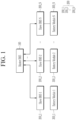
FIG. 1 shows a system for allocating communication IDs according to an embodiment. -
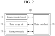
FIG. 2 shows a detailed block diagram on a configuration of a master BMS ofFIG. 1 . -
FIG. 3 shows a detailed block diagram on a configuration of a slave BMS ofFIG. 1 . -
FIG. 4 shows a block diagram on a plurality of slave BMSs sequentially connected to a power line and a corresponding difference of a first current amount according to an embodiment. -
FIG. 5 shows a circuit diagram of a top-level slave BMS shown inFIG. 4 . -
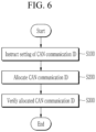
FIG. 6 shows a flowchart of a method for allocating communication IDs according to an embodiment. -
FIG. 7 shows a detailed flowchart of allocating CAN communication IDs ofFIG. 6 (S200). -
FIG. 1 shows a system for allocating communication IDs according to an embodiment,FIG. 2 shows a detailed block diagram on a configuration of a master BMS ofFIG. 1 , andFIG. 3 shows a detailed block diagram on a configuration of a slave BMS ofFIG. 1 . - Referring to
FIG. 1 , the system for allocating communication IDs includes amaster BMS 100 and a plurality of slave BMSs 200_1 to 200_N. - The system for allocating communication IDs is not limited to titles of the
master BMS 100 and the slave BMSs 200_1 to 200_N, and it may be applied to or included in a system including a plurality of control devices and a higher-level control device for managing the control devices in an integrated way. For example, the system for allocating communication IDs may be applied to or included in a battery system or an energy storage system (ESS), but is not limited thereto. - The master BMS 100 may be a higher-level control device for controlling the slave BMSs 200_1 to 200_N in an integrated way. For this purpose, the
master BMS 100 may communicate with the slave BMSs 200_1 to 200_N so as to request necessary information and receive it. Themaster BMS 100 may perform 1:1 communication or 1:N communication with the slave BMSs 200_1 to 200_N according to a controller area network (CAN) communication method, and may identify the slave BMSs 200_1 to 200_N through the communication IDs. - Referring to
FIG. 2 , themaster BMS 100 may include amaster communication unit 110, amaster storage unit 130, amaster power unit 150, and amaster control unit 170. - The
master communication unit 110 may include a communication module for communicating with the slave BMSs 200_1 to 200_N. Depending on embodiments, themaster communication unit 110 may include a CAN communication module. - The
master storage unit 130 may store a number (N) of the slave BMSs 200_1 to 200_N, a plurality of first current amounts applied to the respective slave BMSs 200_1 to 200_N, and a communication ID allocating table on which a plurality of communication IDs corresponding to the first current amounts are recorded. - The
master power unit 150 may supply a power voltage to the slave BMSs 200_1 to 200_N. Depending on embodiments, a power source for supplying a power voltage to the slave BMSs 200_1 to 200_N may, for example, be a low voltage auxiliary battery that is different from the highvoltage battery module 300. For another example, the power source may be realized with amaster power unit 150 for supplying low-voltage power. - The
master control unit 170 may generally control themaster BMS 100, and may integrally manage the slave BMSs 200_1 to 200_N. Depending on embodiments, themaster control unit 170 may broadcast a signal for instructing allocation of communication IDs in the case of first connection to the slave BMSs 200_1 to 200_N through themaster communication unit 110. The slave BMSs 200_1 to 200_N connected to themaster communication unit 110 through the network may automatically allocate the communication IDs. - Depending on embodiments, when receiving a power voltage from the power source, the
master control unit 170 may broadcast a signal for instructing allocation of communication IDs through themaster communication unit 110. - The slave BMS 200 may monitor and control the electrically connected
battery module 300. For example, the slave BMSs 200_1 to 200_N may measure or predict states (e.g., a temperature, a voltage, and charging capacity) of the battery cell included in a plurality of battery modules 300_1 to 300_N and may send resultant signals to themaster BMS 100. The slave BMS 200 may control (e.g., charge and discharge, planarize, etc.) thebattery module 300 according to a control signal received from themaster BMS 100. - Depending on embodiments, the slave BMSs 200_1 to 200_N may be sequentially connected to a power supplying line. For example, the first slave BMS 200_1 and the second slave BMS 200_2 may be connected thereto, and the second slave BMS 200_2 and the third slave BMS 200_3 may be sequentially connected thereto (i.e., the daisy chain method) to receive a consumed current. Accordingly, the
respective slave BMSs 200 may output a second current amount that is generated by subtracting the consumed current amount used for driving from the first current amount applied through the power line through a power line. - In detail, the first current amount applied to the uppermost first slave BMS 200_1 connected near the power source may correspond to the current amount that is a summation of the consumed current amounts of the slave BMSs 200_1 to 200_N. A second current amount output from the uppermost first slave BMS 200_1 may correspond to the current amount generated by subtracting the consumed current amount for driving the first slave BMS 200_1 from the first current amount. The first current amount applied to the lowermost N-th slave BMS 200_N may correspond to the consumed current amount for driving the N-th slave BMS 200_N. In this instance, the N-th slave BMS 200_N has no posterior slave BMS, so the second current amount output from the N-th slave BMS 200_N may not exist, which will be described in detail with reference to
FIG. 4 andFIG. 5 . - Referring to
FIG. 3 , the slave BMS 200 may include aslave communication unit 210, aslave storage unit 230, acurrent measurement unit 250, and aslave control unit 270. - The
slave communication unit 210 may include a communication module for communicating with themaster BMS 100. Depending on embodiments, theslave communication unit 210 may include a CAN communication module. - The
slave storage unit 230 may store information for indicating resistance of the shunt resistor included in thecurrent measurement unit 250, and a communication ID allocating table transmitted from themaster BMS 100 through theslave communication unit 210. - The
current measurement unit 250 includes a shunt resistor coupled in series to the power line, and provides a voltage value that corresponds to a voltage drop caused by the shunt resistor so as to measure a first current amount applied through the power line. For example, theslave control unit 270 may measure voltages at the front end and the rear end of the shunt resistor to calculate a voltage value that corresponds to the voltage drop, and substitutes the calculated voltage value and the resistance of the shunt resistor into Ohm's law to calculate the first current amount (current value). - The
slave control unit 270 generally controls the slave BMS 200. Depending on embodiments, theslave control unit 270 may automatically allocate a predetermined communication ID as the communication ID of theslave control unit 270 based on the first current amount indicating relative positions among the slave BMSs 200_1 to 200_N. -
FIG. 4 shows a block diagram on a plurality of slave BMSs sequentially connected to a power line and a corresponding difference of a first current amount according to an embodiment. - Referring to
FIG. 4 , for example, it will be assumed that the number (N) of the slave BMSs 200_1 to 200_N is 5, the power source supplies a power voltage that corresponds to a predetermined voltage value of 10 V and a predetermined current value of 300 mA, and the consumed current amounts of the respective slave BMSs 200_1 to 200_N are 60 mA. Here, the slave BMSs 200_1 to 200_N may have the same consumed current amount within a predetermined error range (e.g., ±10 mA). - Depending on embodiments, the first to fifth slave BMSs 200_1 to 200_N are sequentially connected to the power supplying line (Ls). In detail, the
uppermost slave BMS 200 may be a first slave BMS 200_1 connected near the power source, and the second to fourth slaves BMS 200_2 to 200_4 may be sequentially connected to the first slave BMS 200_1. Here, the fifth slave BMS 200_5 may correspond to thelowermost slave BMS 200. - As they are sequentially connected to the power line (Ls), the respective first to fifth slave BMSs 200_1 to 200_N output the second current amount that is generated by subtracting the consumed current amount for driving from the first current amount applied through the power line (Ls) to the power line (Ls). A current input with reference to the
predetermined slave BMS 200 is a first current, and a current output therewith is a second current. - In detail, the first current amount applied to the uppermost slave BMS 200_1 may correspond to the entire consumed current amount to be used by the slave BMSs 200_1 to 200_N, that is, the summation value of the consumed current amounts of the slave BMSs 200_1 to 200_N. The first current amounts applied to the respective slave BMSs are gradually reduced while passing through a plurality of intermediate slave BMSs 200_2 to 200_N-1 sequentially connected through the power line (Ls). The lowermost slave BMS 200_N may receive the first current amount corresponding to the consumed current amount to be used by the lowermost slave BMS 200_N. In this instance, the lowermost slave BMS 200_N has no posterior slave BMS, so there may be no second current amount output by the lowermost slave BMS 200_N.
- For example, referring to
FIG. 4 , the first current amount applied to the first slave BMS 200_1 through a first input end (IN1) may be 300 mA that is the summation of the consumed current amount of 60 mA of the first to fifth slave BMSs 200_1 to 200_5. The second current amount output by the first slave BMS 200_1 may correspond to the current amount (240 mA = 300 mA - 60 mA) generated by subtracting the consumed current amount of 60 mA of the first slave BMS 200_1 from the first current amount of 300 mA. The consumed current amount of 60 mA is gradually reduced while passing through the second to fourth slave BMSs 200_2 to 200_4, and the first current amount is sequentially reduced (240 mA, 180 mA, and 120 mA) by the consumed current amount. The first current amount applied to the fifth slave BMS 200_5 may correspond to the consumed current amount of 60 mA of the fifth slave BMS 200_5. - As described above, the first current amount corresponds to the summation of the consumed current amounts of the
slave BMS 200 for receiving the first current amount and the sequentially connectedposterior slave BMS 200. Assuming that consumed current amounts of therespective slave BMSs 200 have a same value within a predetermined error range, the first current amount may indicate (or express) the relative positions of the slave BMSs 200_1 to 200_N. - Depending on embodiments, the first current amount (e.g., 300 mA) may be expressed as a predetermined multiple (300 mA/60 mA = 5) of the consumed current amount of 60 mA, and the predetermined multiple of 5 may correspond to the number (N=5) of the sequentially
connected slave BMSs 200. - Referring to
FIG. 4 , the first current amount of 300 mA indicates that there are five (300 mA/60 mA = 5)slave BMSs 200 that are sequentially connected, so theslave BMS 200 receiving the first current amount of 300 mA may be afifth slave BMS 200 from the lowermost slave BMS 200_5. In this instance, since the number (N) of the slave BMSs 200_1 to 200_N is 5, theslave BMS 200 receiving the first current amount of 300 mA may be the uppermost slave BMS 200_1. When calculated by the same method, theslave BMS 200 receiving the first current amount of 60 mA may be thelowermost slave BMS 200. -
FIG. 5 shows a circuit diagram of a top-level slave BMS shown inFIG. 4 . - Referring to
FIG. 4 andFIG. 5 , according to an embodiment, when themaster BMS 100 broadcasts the signal for instructing allocation of communication IDs through a network, the first slave BMS 200_1 may calculate a first current amount (11) applied through the first input end (IN1) of the power line (LS), and may allocate a predetermined communication ID as the communication ID of the first slave BMS 200_1 based on the calculated first current amount (11). Depending on embodiments, a second current (12) output by the first slave BMS 200_1 through the power line (LS) may be applied as a first current of the second slave BMS 200_2. - The
slave control unit 270 measures voltages at a first node N11 positioned at the front end of the shunt resistor R1 coupled in series to the power line (LS) and a second node N12 positioned at the rear end thereof. For example, theslave control unit 270 may reduce the voltages respectively measured at the first node N11 and the second node N12 into values that are within an input range, and may then receive them. For this purpose, a plurality of resistors R11 to R14 may be disposed in series and/or in parallel between the shunt resistor R1 and theslave control unit 270. For example, respective resistance of the resistors R11 to R14 may set so that the voltages (about 10 V and 9.7 V) measured at the first node N11 and the second node N12 may be reduced by the ratio of 1/10 (about 1 V and 0.97 V) and may be applied to theslave control unit 270. Depending on embodiments, theslave control unit 270 may be realized as a microcontroller unit (MCU). - The
slave control unit 270 calculates a difference value (10 V - 9.7 V = 0.3 V) between the voltage value (e.g., 10 V) measured at the first node (N11) and the voltage value (e.g., 9.7 V) measured at the second node N12, that is, the voltage value (0.3 V) caused by a voltage drop (↓) of the shunt resistor R1. Theslave control unit 270 may substitute (I=V/R) the resistance (e.g., 1 Ω) of the shunt resistor R1 stored in theslave storage unit 230 and the voltage value (0.3 V) caused by the voltage drop (↓) of the shunt resistor R1 into Ohm's law to calculate the first current amount (I = 0.3 V/1 Ω = 300 mA). - The
slave control unit 270 may automatically allocate the communication ID that corresponds to the calculated first current amount of 300 mA as the communication ID of theslave control unit 270 based on the communication ID allocating table. The communication ID allocating table may, as expressed in Table 1, include a plurality of communication IDs that correspond to a plurality of first current amounts (11 to I5) respectively.(Table 1) First current (I) Communication IDs Relative positions 300 mA (11) ID_1 N=1 240 mA (12) ID_2 N=2 180 mA (13) ID_3 N=3 120 mA (14) ID_4 N=4 60 mA (15) ID_5 N=5 - Referring to Table 1, the first slave BMS 200_1 corresponding to N=1 is the
uppermost slave BMS 200, and the fifth slave BMS 200_5 corresponding to N=5 is thelowermost slave BMS 200. For example, theslave control unit 270 of the first slave BMS 200_1 may automatically allocate the first communication ID (ID_1) that corresponds to the calculated first current amount of 300 mA as the communication ID of theslave control unit 270 based on the communication ID allocating table. - Referring to
FIG. 5 , theslave control unit 270 may receive a current for driving, that is, the consumed current (Icc) from the third node N13 positioned at the rear end of the second node N12. For example, the consumed current amount (Icc) may be 60 mA. The second current amount (12) output by the first slave BMS 200_1 through the power line (LS) may correspond to the current amount (240 mA = 300 mA - 60 mA) that is the first current amount of 300 mA minus the consumed current amount 60 mA used by the first slave BMS 200_1. - Referring to
FIG. 4 andFIG. 5 , the second to fifth slave BMSs 200_2 to 200_5 may respectively include the same circuit configuration as the first slave BMS 200_1 described with reference toFIG. 5 . The resistance (e.g., 1 Ω) of the shunt resistor R1 included in the respective second to fifth slave BMSs 200_2 to 200_5 may be the same. The respective second to fifth slave BMSs 200_2 to 200_5 may calculate the first current amounts (12 to I5) applied through the second to fifth input ends (IN2 to IN5) of the power line (LS). - Referring to
FIG. 4 , regarding the second slave BMS 200_2, the voltage value caused by the voltage drop (↓) of the shunt resistor R1 is 0.24 V (9.7 V - 9.46 V = 0.24 V). The first current amount (I = 0.24 V / 1 Ω = 240 mA) applied through the second input end (IN2) of the power line (LS) may be calculated by substituting (I=V/R) resistance of 1 Ω of the shunt resistor R1 and the voltage value of 0.24 V caused by the voltage drop (↓) of the shunt resistor R1 into Ohm's law. With the same calculation method, the first current amounts applied to the respective third to fifth slave BMSs 200_2 to 200_5 through the second to fifth input ends (IN2 to IN5) may be calculated to be 180 mA, 120 mA, and 60 mA as shown inFIG. 4 . - The respective second to fifth slave BMSs 200_2 to 200_5 may automatically allocate the communication IDs (ID_2, ID_3, ID_4, and ID_5) that correspond to the calculated first current amounts of 240 mA, 180 mA, 120 mA, and 60 mA as the communication IDs of the second to fifth slave BMSs 200_2 to 200_5 based on the communication ID allocating table. The second slave BMS 200_2 may automatically allocate the second communication ID (ID_2) as the communication ID of the second slave BMS 200_2. In a like way, the third slave BMS 200_3 to fifth slave BMS 200_5 may automatically allocate the third communication ID (ID_3), the fourth communication ID (ID_4), and the fifth communication ID (ID_5) as the communication IDs of the third slave BMS 200_3 to the fifth slave BMS 200_5.
-
FIG. 6 shows a flowchart of a method for allocating communication IDs according to an embodiment. -
FIG. 7 shows a detailed flowchart of allocating CAN communication IDs ofFIG. 6 (S200). A method for allocating communication IDs will now be described with reference toFIG. 1 to FIG. 7 . - Referring to
FIG. 6 , themaster BMS 100 may broadcast a signal for instructing allocation of communication IDs through the network in the case of the first connection to the slave BMSs 200_1 to 200_N (S100). - In order for the
master BMS 100 to communicate with the slave BMSs 200_1 to 200_N, communication IDs for identifying the slave BMSs 200_1 to 200_N are needed. However, themaster BMS 100 may not specify the respective slave BMSs 200_1 to 200_N and may not transmit signals before the communication IDs are allocated, so it may broadcast the communication ID allocating instruction to the slave BMSs 200_1 to 200_N through the network. - Depending on embodiments, the
master BMS 100 may broadcast the signal for instructing allocation of communication IDs when power is supplied from the power source through a power line. - The
slave BMS 200 may allocate a predetermined communication ID as the communication ID of theslave BMS 200 based on the first current amount applied through the power line (S200). - Depending on embodiments, the slave BMSs 200_1 to 200_N are sequentially connected to the power line for supplying power. The slave BMSs 200_1 to 200_N may output the second current amount that is the first current amount minus the consumed current amount for driving through the power line. For example, the first current amount may correspond to the summation value of the consumed current amount of the
slave BMS 200 receiving the first current amount and the consumed current amount of at least oneposterior slave BMS 200 sequentially connected to theslave BMS 200 receiving the first current amount. - Referring to
FIG. 6 , in S200, theslave BMS 200 may measure the voltages at the front end and the rear end of the shunt resistor R1 coupled in series to the power line and may calculate the voltage value caused by the voltage drop (S210). - The
slave control unit 270 may measure the voltages at the first node N11 of the front end of the shunt resistor R1 coupled in series to the power line (LS) and the second node N12 of the rear end thereof. Referring toFIG. 5 , for example, theslave control unit 270 included in the first slave BMS 200_1 may calculate the difference value (10 V - 9.7 V = 0.3 V) between the voltage value (e.g., 10 V) at the front end N11 of the shunt resistor R1 and the voltage value (e.g., 9.7 V) at the rear end N12, that is, the voltage value (0.3 V) caused by the voltage drop (↓) of the shunt resistor R1. - In S200, the
slave BMS 200 may calculate the first current amount based on the voltage value caused by the voltage drop (↓) of the shunt resistor R1 and the resistance of the shunt resistor R1 (S230). - The
slave control unit 270 may substitute (I=V/R) the resistance (e.g., 1 Ω) of the shunt resistor R1 and the voltage value (0.3 V) caused by the voltage drop (↓) of the shunt resistor R1 into Ohm's law and may calculate the first current amount (I = 0.3 V/1 Ω = 300 mA). The resistance of the shunt resistor R1 may be stored in theslave storage unit 230. - According to the above-noted method, the second to fifth slave BMSs 200_2 to 200_5 may respectively calculate the first current amounts. For example, the first current amounts of the second to fifth slave BMS 200_2 to 200_N may be 240 mA, 180 mA, 120 mA, and 60 mA.
- In S200, the
slave BMS 200 may allocate the communication ID that corresponds to the first current amount as the communication ID of theslave BMS 200 based on the communication ID allocating table (S250). Here, as expressed in Table 1, the communication ID allocating table may include a plurality of communication IDs that correspond to a plurality of first current amounts (11 to I5). - The
master BMS 100 may receive the calculated first current amounts and the allocated communication IDs from the slave BMSs 200_1 to 200_N, and may verify the allocated communication IDs (S300). - For example, the
master BMS 100 may receive the first current amount of 330 mA and the second communication ID (ID_2) from the second slave BMS 200_2, and may compare them with the communication ID allocating table to verify the second communication ID. Referring to Table 1, the first current amount corresponding to the second communication ID (ID_2) is 240 mA. This is different from the first current amount 330 mA and the communication ID (ID_2) received from the second slave BMS 200_2. Themaster BMS 100 may determine the allocation of communication IDs performed by the second slave BMS 200_2 to have errors. - When the allocation of communication IDs by at least one of the slave BMSs 200_1 to 200_N is found to be erroneous, the
master BMS 100 may broadcast an instruction for instructing allocation of communication IDs to the slave BMSs 200_1 to 200_N.
Claims (6)
- A system for allocating communication IDs comprising:a plurality of slave battery management systems(200_1, 200_2, ..., 200_N), BMSs, sequentially connected to a power line (Ls) for supplying power, and allocating predetermined communication IDs based on first current amounts applied through the power line to enter each of the slave BMSs,wherein each of the slave BMSs is configured to consume a current amount (Icc) through the power line for driving and output a second current amount that is the first current amount applied thereto, minus the consumed current amount, and that is the first current amount applied to the slave BMS next in line in the BMS sequence;wherein each slave BMS includes:a shunt resistor (R1) coupled in series to the power line;a slave storage (230) for storing information for indicating resistance of the shunt resistor and a communication ID allocating table in which a plurality of communication IDs correspond to a plurality of first current amounts are recorded; anda slave controller (270) for measuring voltages at a front end and a rear end of the shunt resistor to calculate a voltage value caused by a voltage drop, calculating the first current amount based on the voltage value and resistance of the shunt resistor, and allocating a communication ID based on the calculated first current amount and the communication ID allocating table,wherein the system further comprisesa master BMS (100) including the communication ID allocating table in which a plurality of communication IDs corresponding to a number of the slave BMSs and the first current amounts are recorded into a signal for instructing allocation of the communication IDs and broadcasting the same,the master BMS being configured to receive the calculated first current amounts and the allocated communication ID from the slave BMSs, and compares the received first current amounts and the received communication IDs and the communication ID allocating table to verify allocation of communication IDs of the slave BMSs.
- The system of claim 1, whereineach of the slave BMSs further includes a slave communicator (210) for communicating with the master BMS and receiving the signal, andthe slave controller is configured to measure voltages at a front end and a rear end of the shunt resistor and calculate the first current amount upon receiving the signal through the slave communicator.
- The system of claim 2, wherein
each of the slave controller is configured to allocate the communication ID that corresponds to the calculated first current amount as the communication ID of the slave controller based on the communication ID allocating table. - The system of claim 1, wherein
the communication ID is an ID for controller area network, CAN, communication. - The system of claim 1, wherein
the master BMS is operable by a power source for supplying the power to the slave BMSs. - A method for allocating communication IDs of a plurality of slave battery management systems, BMSs, sequentially connected to a power line for supplying power based on first current amounts applied through the power line to each of the slave BMSs, comprisingallowing the slave BMSs to allocate predetermined communication IDs as communication IDs of the slave BMSs based on the first current amounts,wherein each of the slave BMSs consumes a current amount through the power line for driving and outputs a second current amount that is the first current amount applied thereto minus the consumed current amount, and that is the first current amount applied to the slave BMS next in line in the BMS sequence,whereinthe allocating of predetermined communication IDs as communication IDs of the slave BMSs based on the first current amount includes:measuring voltages at a front end and a rear end of a shunt resistor coupled in series to the power line and calculating a voltage value caused by a voltage drop;calculating the first current amount based on the voltage value and resistance of the shunt resistor; andallocating the communication ID that corresponds to the calculated first current amount as the communication of the slave BMS ID based on a communication ID allocating table in which a plurality of communication IDs corresponding to a plurality of first current amounts are recorded,wherein the method further comprises,after the allocating of predetermined communication IDs as communication IDs of the slave BMSs based on the first current amount,allowing a master BMS to receive the calculated first current amount and the allocated communication ID from the slave BMSs, and verify allocation of communication IDs of the respective slave BMSs.
Applications Claiming Priority (2)
| Application Number | Priority Date | Filing Date | Title |
|---|---|---|---|
| KR1020200148613A KR20220062887A (en) | 2020-11-09 | 2020-11-09 | Method for assigning communication id and system providing the same |
| PCT/KR2021/010604 WO2022097884A1 (en) | 2020-11-09 | 2021-08-10 | Method for assigning communication id and system providing same |
Publications (3)
| Publication Number | Publication Date |
|---|---|
| EP4030700A1 EP4030700A1 (en) | 2022-07-20 |
| EP4030700A4 EP4030700A4 (en) | 2022-11-23 |
| EP4030700B1 true EP4030700B1 (en) | 2025-03-26 |
Family
ID=81457935
Family Applications (1)
| Application Number | Title | Priority Date | Filing Date |
|---|---|---|---|
| EP21876736.6A Active EP4030700B1 (en) | 2020-11-09 | 2021-08-10 | Method for allocating communication id and system providing the method |
Country Status (8)
| Country | Link |
|---|---|
| US (1) | US20240235886A9 (en) |
| EP (1) | EP4030700B1 (en) |
| JP (1) | JP7438601B2 (en) |
| KR (1) | KR20220062887A (en) |
| CN (1) | CN114830612B (en) |
| ES (1) | ES3024980T3 (en) |
| HU (1) | HUE071174T2 (en) |
| WO (1) | WO2022097884A1 (en) |
Families Citing this family (2)
| Publication number | Priority date | Publication date | Assignee | Title |
|---|---|---|---|---|
| CN117614028B (en) * | 2023-11-22 | 2024-08-30 | 湖南三江电力有限责任公司 | On-line monitoring, distributing, regulating and analyzing system for load of hydroelectric generating set |
| KR20260033890A (en) * | 2024-09-03 | 2026-03-10 | 주식회사 엘지에너지솔루션 | The method for assigning communication ID and system providing the same |
Family Cites Families (19)
| Publication number | Priority date | Publication date | Assignee | Title |
|---|---|---|---|---|
| JP2006165957A (en) | 2004-12-07 | 2006-06-22 | Victor Co Of Japan Ltd | Serial communication system and address setting method |
| US8122159B2 (en) * | 2009-01-16 | 2012-02-21 | Allegro Microsystems, Inc. | Determining addresses of electrical components arranged in a daisy chain |
| JP2011035817A (en) | 2009-08-05 | 2011-02-17 | Denso Corp | Communication device for crew protection system |
| KR101245279B1 (en) * | 2010-10-11 | 2013-03-19 | 주식회사 엘지화학 | Method and System for setting up sequent ID of multi-slave in battery pack |
| JP5220159B2 (en) | 2011-04-08 | 2013-06-26 | 三菱電機株式会社 | Power converter address automatic setting method and photovoltaic power generation system to which this method is applied |
| US8775689B2 (en) * | 2011-05-02 | 2014-07-08 | Deere & Company | Electronic modules with automatic configuration |
| KR101386080B1 (en) * | 2011-09-05 | 2014-04-17 | 주식회사 엘지화학 | Method and system for identifier allowcation of multi-slave in battery pack |
| KR101539689B1 (en) * | 2012-02-20 | 2015-07-27 | 주식회사 엘지화학 | System and method for identifier allowcation of multi-bms |
| JP5902133B2 (en) | 2013-08-30 | 2016-04-13 | プライムアースEvエナジー株式会社 | Power supply |
| KR101632350B1 (en) | 2013-09-09 | 2016-06-21 | 주식회사 엘지화학 | System and method for communication identifier allowcation of multi-bms |
| KR20150125433A (en) * | 2014-04-30 | 2015-11-09 | 삼성전자주식회사 | Method and apparatus for generating identifier of slave device |
| KR102059613B1 (en) * | 2015-11-05 | 2019-12-26 | 주식회사 엘지화학 | System and method of controlling battery pack for parallel expansion |
| KR102123671B1 (en) * | 2016-02-22 | 2020-06-16 | 주식회사 엘지화학 | Method allocating identifier for battery management system |
| US10886753B2 (en) * | 2017-02-13 | 2021-01-05 | O2Micro Inc. | Systems and methods for managing a battery pack |
| KR102155331B1 (en) * | 2017-07-06 | 2020-09-11 | 주식회사 엘지화학 | Wireless battery manamement system and a battery pack including the same |
| JP2020053176A (en) | 2018-09-25 | 2020-04-02 | 株式会社デンソー | Battery monitoring system |
| KR102680186B1 (en) * | 2018-10-10 | 2024-06-28 | 주식회사 엘지에너지솔루션 | System and method for automatically assigning an identifier of a bms using a pwm signal |
| JP7047748B2 (en) | 2018-12-19 | 2022-04-05 | 株式会社デンソー | Communications system |
| KR102405847B1 (en) * | 2019-01-10 | 2022-06-03 | 주식회사 엘지에너지솔루션 | Apparatus for managing battery and battery pack including the same |
-
2020
- 2020-11-09 KR KR1020200148613A patent/KR20220062887A/en active Pending
-
2021
- 2021-08-10 WO PCT/KR2021/010604 patent/WO2022097884A1/en not_active Ceased
- 2021-08-10 ES ES21876736T patent/ES3024980T3/en active Active
- 2021-08-10 JP JP2022519317A patent/JP7438601B2/en active Active
- 2021-08-10 CN CN202180005988.9A patent/CN114830612B/en active Active
- 2021-08-10 HU HUE21876736A patent/HUE071174T2/en unknown
- 2021-08-10 US US17/769,956 patent/US20240235886A9/en active Pending
- 2021-08-10 EP EP21876736.6A patent/EP4030700B1/en active Active
Also Published As
| Publication number | Publication date |
|---|---|
| HUE071174T2 (en) | 2025-08-28 |
| EP4030700A1 (en) | 2022-07-20 |
| ES3024980T3 (en) | 2025-06-05 |
| JP7438601B2 (en) | 2024-02-27 |
| EP4030700A4 (en) | 2022-11-23 |
| WO2022097884A1 (en) | 2022-05-12 |
| KR20220062887A (en) | 2022-05-17 |
| CN114830612B (en) | 2024-05-17 |
| US20240137245A1 (en) | 2024-04-25 |
| JP2023504342A (en) | 2023-02-03 |
| CN114830612A (en) | 2022-07-29 |
| US20240235886A9 (en) | 2024-07-11 |
Similar Documents
| Publication | Publication Date | Title |
|---|---|---|
| JP4342583B2 (en) | Battery management system and battery management system driving method | |
| US9768624B2 (en) | Method for cell balancing for a plurality of battery cells, and battery system for performing such a method | |
| EP4030700B1 (en) | Method for allocating communication id and system providing the method | |
| US20080233471A1 (en) | Battery State Detection | |
| KR20180079771A (en) | Battery management apparatus and soc calibrating method using the same | |
| JP2011041452A (en) | Assembled battery unit and vehicle | |
| US20190146039A1 (en) | Method for Determining the Internal Resistance of Battery Cells, Battery Module, and Device | |
| KR102824433B1 (en) | Method for estimating of battery's state of charge and Battery Management System | |
| EP4083642B1 (en) | Fault cell diagnosis method and battery system using same | |
| US11598819B2 (en) | Method for ascertaining a charge state of a battery system, battery system | |
| US10756393B2 (en) | Method for preventing duplicate allocation of ID to battery modules | |
| US12603800B2 (en) | Terminating resistance setting circuit and battery management system including same | |
| KR102892946B1 (en) | Current calibration method for current sensor and battery system providing the same | |
| CN218996826U (en) | Battery management system and battery system | |
| US12304537B2 (en) | Railway carriage with vehicle monitoring system and associated monitoring method | |
| KR102929046B1 (en) | Method for estimating dcir of battery and battery system providing the same | |
| EP4583359A1 (en) | Method and apparatus for setting battery pack identifier | |
| KR102807862B1 (en) | Battery management device using complex monitering and method of managing the system | |
| KR102892941B1 (en) | Battery system | |
| KR102818350B1 (en) | Battery module, battery management system and method | |
| KR20260011485A (en) | Electrified vehicle providing battery partial replacement mode and method of controlling the same | |
| CN116061722A (en) | Modular charger with contact assignment diagnostic function of contact elements and method thereof | |
| KR20240066956A (en) | Battery system and parallel packs control method using the same | |
| KR20240145348A (en) | Battery module and method of operating the same | |
| KR20240163388A (en) | Management method for battery data and battery management system providing the same |
Legal Events
| Date | Code | Title | Description |
|---|---|---|---|
| STAA | Information on the status of an ep patent application or granted ep patent |
Free format text: STATUS: UNKNOWN |
|
| STAA | Information on the status of an ep patent application or granted ep patent |
Free format text: STATUS: THE INTERNATIONAL PUBLICATION HAS BEEN MADE |
|
| PUAI | Public reference made under article 153(3) epc to a published international application that has entered the european phase |
Free format text: ORIGINAL CODE: 0009012 |
|
| STAA | Information on the status of an ep patent application or granted ep patent |
Free format text: STATUS: REQUEST FOR EXAMINATION WAS MADE |
|
| 17P | Request for examination filed |
Effective date: 20220413 |
|
| AK | Designated contracting states |
Kind code of ref document: A1 Designated state(s): AL AT BE BG CH CY CZ DE DK EE ES FI FR GB GR HR HU IE IS IT LI LT LU LV MC MK MT NL NO PL PT RO RS SE SI SK SM TR |
|
| A4 | Supplementary search report drawn up and despatched |
Effective date: 20221020 |
|
| RIC1 | Information provided on ipc code assigned before grant |
Ipc: H04L 12/40 20060101AFI20221014BHEP |
|
| DAV | Request for validation of the european patent (deleted) | ||
| DAX | Request for extension of the european patent (deleted) | ||
| STAA | Information on the status of an ep patent application or granted ep patent |
Free format text: STATUS: EXAMINATION IS IN PROGRESS |
|
| 17Q | First examination report despatched |
Effective date: 20240410 |
|
| GRAP | Despatch of communication of intention to grant a patent |
Free format text: ORIGINAL CODE: EPIDOSNIGR1 |
|
| STAA | Information on the status of an ep patent application or granted ep patent |
Free format text: STATUS: GRANT OF PATENT IS INTENDED |
|
| RIC1 | Information provided on ipc code assigned before grant |
Ipc: H02J 7/00 20060101ALI20240911BHEP Ipc: H01M 10/42 20060101ALI20240911BHEP Ipc: H04L 12/40 20060101AFI20240911BHEP |
|
| INTG | Intention to grant announced |
Effective date: 20240919 |
|
| P01 | Opt-out of the competence of the unified patent court (upc) registered |
Free format text: CASE NUMBER: APP_56685/2024 Effective date: 20241017 |
|
| GRAJ | Information related to disapproval of communication of intention to grant by the applicant or resumption of examination proceedings by the epo deleted |
Free format text: ORIGINAL CODE: EPIDOSDIGR1 |
|
| STAA | Information on the status of an ep patent application or granted ep patent |
Free format text: STATUS: EXAMINATION IS IN PROGRESS |
|
| GRAP | Despatch of communication of intention to grant a patent |
Free format text: ORIGINAL CODE: EPIDOSNIGR1 |
|
| STAA | Information on the status of an ep patent application or granted ep patent |
Free format text: STATUS: GRANT OF PATENT IS INTENDED |
|
| INTC | Intention to grant announced (deleted) | ||
| GRAS | Grant fee paid |
Free format text: ORIGINAL CODE: EPIDOSNIGR3 |
|
| INTG | Intention to grant announced |
Effective date: 20250115 |
|
| GRAA | (expected) grant |
Free format text: ORIGINAL CODE: 0009210 |
|
| STAA | Information on the status of an ep patent application or granted ep patent |
Free format text: STATUS: THE PATENT HAS BEEN GRANTED |
|
| AK | Designated contracting states |
Kind code of ref document: B1 Designated state(s): AL AT BE BG CH CY CZ DE DK EE ES FI FR GB GR HR HU IE IS IT LI LT LU LV MC MK MT NL NO PL PT RO RS SE SI SK SM TR |
|
| REG | Reference to a national code |
Ref country code: GB Ref legal event code: FG4D |
|
| REG | Reference to a national code |
Ref country code: CH Ref legal event code: EP |
|
| REG | Reference to a national code |
Ref country code: DE Ref legal event code: R096 Ref document number: 602021028302 Country of ref document: DE |
|
| REG | Reference to a national code |
Ref country code: IE Ref legal event code: FG4D |
|
| REG | Reference to a national code |
Ref country code: ES Ref legal event code: FG2A Ref document number: 3024980 Country of ref document: ES Kind code of ref document: T3 Effective date: 20250605 |
|
| PG25 | Lapsed in a contracting state [announced via postgrant information from national office to epo] |
Ref country code: RS Free format text: LAPSE BECAUSE OF FAILURE TO SUBMIT A TRANSLATION OF THE DESCRIPTION OR TO PAY THE FEE WITHIN THE PRESCRIBED TIME-LIMIT Effective date: 20250626 |
|
| PG25 | Lapsed in a contracting state [announced via postgrant information from national office to epo] |
Ref country code: FI Free format text: LAPSE BECAUSE OF FAILURE TO SUBMIT A TRANSLATION OF THE DESCRIPTION OR TO PAY THE FEE WITHIN THE PRESCRIBED TIME-LIMIT Effective date: 20250326 |
|
| REG | Reference to a national code |
Ref country code: LT Ref legal event code: MG9D |
|
| PG25 | Lapsed in a contracting state [announced via postgrant information from national office to epo] |
Ref country code: NO Free format text: LAPSE BECAUSE OF FAILURE TO SUBMIT A TRANSLATION OF THE DESCRIPTION OR TO PAY THE FEE WITHIN THE PRESCRIBED TIME-LIMIT Effective date: 20250626 |
|
| PGFP | Annual fee paid to national office [announced via postgrant information from national office to epo] |
Ref country code: BE Payment date: 20250417 Year of fee payment: 5 |
|
| PG25 | Lapsed in a contracting state [announced via postgrant information from national office to epo] |
Ref country code: HR Free format text: LAPSE BECAUSE OF FAILURE TO SUBMIT A TRANSLATION OF THE DESCRIPTION OR TO PAY THE FEE WITHIN THE PRESCRIBED TIME-LIMIT Effective date: 20250326 |
|
| PG25 | Lapsed in a contracting state [announced via postgrant information from national office to epo] |
Ref country code: LV Free format text: LAPSE BECAUSE OF FAILURE TO SUBMIT A TRANSLATION OF THE DESCRIPTION OR TO PAY THE FEE WITHIN THE PRESCRIBED TIME-LIMIT Effective date: 20250326 |
|
| PG25 | Lapsed in a contracting state [announced via postgrant information from national office to epo] |
Ref country code: GR Free format text: LAPSE BECAUSE OF FAILURE TO SUBMIT A TRANSLATION OF THE DESCRIPTION OR TO PAY THE FEE WITHIN THE PRESCRIBED TIME-LIMIT Effective date: 20250627 Ref country code: BG Free format text: LAPSE BECAUSE OF FAILURE TO SUBMIT A TRANSLATION OF THE DESCRIPTION OR TO PAY THE FEE WITHIN THE PRESCRIBED TIME-LIMIT Effective date: 20250326 |
|
| REG | Reference to a national code |
Ref country code: NL Ref legal event code: MP Effective date: 20250326 |
|
| PG25 | Lapsed in a contracting state [announced via postgrant information from national office to epo] |
Ref country code: NL Free format text: LAPSE BECAUSE OF FAILURE TO SUBMIT A TRANSLATION OF THE DESCRIPTION OR TO PAY THE FEE WITHIN THE PRESCRIBED TIME-LIMIT Effective date: 20250326 |
|
| REG | Reference to a national code |
Ref country code: HU Ref legal event code: AG4A Ref document number: E071174 Country of ref document: HU |
|
| PG25 | Lapsed in a contracting state [announced via postgrant information from national office to epo] |
Ref country code: SE Free format text: LAPSE BECAUSE OF FAILURE TO SUBMIT A TRANSLATION OF THE DESCRIPTION OR TO PAY THE FEE WITHIN THE PRESCRIBED TIME-LIMIT Effective date: 20250326 |
|
| REG | Reference to a national code |
Ref country code: AT Ref legal event code: MK05 Ref document number: 1780073 Country of ref document: AT Kind code of ref document: T Effective date: 20250326 |
|
| PGFP | Annual fee paid to national office [announced via postgrant information from national office to epo] |
Ref country code: HU Payment date: 20250827 Year of fee payment: 5 |
|
| PG25 | Lapsed in a contracting state [announced via postgrant information from national office to epo] |
Ref country code: SM Free format text: LAPSE BECAUSE OF FAILURE TO SUBMIT A TRANSLATION OF THE DESCRIPTION OR TO PAY THE FEE WITHIN THE PRESCRIBED TIME-LIMIT Effective date: 20250326 |
|
| PG25 | Lapsed in a contracting state [announced via postgrant information from national office to epo] |
Ref country code: PT Free format text: LAPSE BECAUSE OF FAILURE TO SUBMIT A TRANSLATION OF THE DESCRIPTION OR TO PAY THE FEE WITHIN THE PRESCRIBED TIME-LIMIT Effective date: 20250728 |
|
| PGFP | Annual fee paid to national office [announced via postgrant information from national office to epo] |
Ref country code: ES Payment date: 20250911 Year of fee payment: 5 |
|
| PGFP | Annual fee paid to national office [announced via postgrant information from national office to epo] |
Ref country code: DE Payment date: 20250721 Year of fee payment: 5 |
|
| PG25 | Lapsed in a contracting state [announced via postgrant information from national office to epo] |
Ref country code: IT Free format text: LAPSE BECAUSE OF FAILURE TO SUBMIT A TRANSLATION OF THE DESCRIPTION OR TO PAY THE FEE WITHIN THE PRESCRIBED TIME-LIMIT Effective date: 20250326 Ref country code: PL Free format text: LAPSE BECAUSE OF FAILURE TO SUBMIT A TRANSLATION OF THE DESCRIPTION OR TO PAY THE FEE WITHIN THE PRESCRIBED TIME-LIMIT Effective date: 20250326 |
|
| PGFP | Annual fee paid to national office [announced via postgrant information from national office to epo] |
Ref country code: GB Payment date: 20250722 Year of fee payment: 5 |
|
| PG25 | Lapsed in a contracting state [announced via postgrant information from national office to epo] |
Ref country code: AT Free format text: LAPSE BECAUSE OF FAILURE TO SUBMIT A TRANSLATION OF THE DESCRIPTION OR TO PAY THE FEE WITHIN THE PRESCRIBED TIME-LIMIT Effective date: 20250326 |
|
| PGFP | Annual fee paid to national office [announced via postgrant information from national office to epo] |
Ref country code: FR Payment date: 20250725 Year of fee payment: 5 |
|
| PG25 | Lapsed in a contracting state [announced via postgrant information from national office to epo] |
Ref country code: EE Free format text: LAPSE BECAUSE OF FAILURE TO SUBMIT A TRANSLATION OF THE DESCRIPTION OR TO PAY THE FEE WITHIN THE PRESCRIBED TIME-LIMIT Effective date: 20250326 |
|
| PG25 | Lapsed in a contracting state [announced via postgrant information from national office to epo] |
Ref country code: RO Free format text: LAPSE BECAUSE OF FAILURE TO SUBMIT A TRANSLATION OF THE DESCRIPTION OR TO PAY THE FEE WITHIN THE PRESCRIBED TIME-LIMIT Effective date: 20250326 |
|
| PG25 | Lapsed in a contracting state [announced via postgrant information from national office to epo] |
Ref country code: SK Free format text: LAPSE BECAUSE OF FAILURE TO SUBMIT A TRANSLATION OF THE DESCRIPTION OR TO PAY THE FEE WITHIN THE PRESCRIBED TIME-LIMIT Effective date: 20250326 |
|
| PG25 | Lapsed in a contracting state [announced via postgrant information from national office to epo] |
Ref country code: IS Free format text: LAPSE BECAUSE OF FAILURE TO SUBMIT A TRANSLATION OF THE DESCRIPTION OR TO PAY THE FEE WITHIN THE PRESCRIBED TIME-LIMIT Effective date: 20250726 |
|
| REG | Reference to a national code |
Ref country code: DE Ref legal event code: R097 Ref document number: 602021028302 Country of ref document: DE |
|
| PG25 | Lapsed in a contracting state [announced via postgrant information from national office to epo] |
Ref country code: DK Free format text: LAPSE BECAUSE OF FAILURE TO SUBMIT A TRANSLATION OF THE DESCRIPTION OR TO PAY THE FEE WITHIN THE PRESCRIBED TIME-LIMIT Effective date: 20250326 |
|
| PG25 | Lapsed in a contracting state [announced via postgrant information from national office to epo] |
Ref country code: CZ Free format text: LAPSE BECAUSE OF FAILURE TO SUBMIT A TRANSLATION OF THE DESCRIPTION OR TO PAY THE FEE WITHIN THE PRESCRIBED TIME-LIMIT Effective date: 20250326 |
|
| PLBE | No opposition filed within time limit |
Free format text: ORIGINAL CODE: 0009261 |
|
| STAA | Information on the status of an ep patent application or granted ep patent |
Free format text: STATUS: NO OPPOSITION FILED WITHIN TIME LIMIT |
|
| REG | Reference to a national code |
Ref country code: CH Ref legal event code: L10 Free format text: ST27 STATUS EVENT CODE: U-0-0-L10-L00 (AS PROVIDED BY THE NATIONAL OFFICE) Effective date: 20260211 |
|
| 26N | No opposition filed |
Effective date: 20260105 |
|
| REG | Reference to a national code |
Ref country code: CH Ref legal event code: H13 Free format text: ST27 STATUS EVENT CODE: U-0-0-H10-H13 (AS PROVIDED BY THE NATIONAL OFFICE) Effective date: 20260324 |
|
| PG25 | Lapsed in a contracting state [announced via postgrant information from national office to epo] |
Ref country code: MC Free format text: LAPSE BECAUSE OF FAILURE TO SUBMIT A TRANSLATION OF THE DESCRIPTION OR TO PAY THE FEE WITHIN THE PRESCRIBED TIME-LIMIT Effective date: 20250326 |
|
| PG25 | Lapsed in a contracting state [announced via postgrant information from national office to epo] |
Ref country code: LU Free format text: LAPSE BECAUSE OF NON-PAYMENT OF DUE FEES Effective date: 20250810 |
|
| PG25 | Lapsed in a contracting state [announced via postgrant information from national office to epo] |
Ref country code: CH Free format text: LAPSE BECAUSE OF NON-PAYMENT OF DUE FEES Effective date: 20250831 |