EP4027354A1 - Flexible wiring member - Google Patents
Flexible wiring member Download PDFInfo
- Publication number
- EP4027354A1 EP4027354A1 EP21218304.0A EP21218304A EP4027354A1 EP 4027354 A1 EP4027354 A1 EP 4027354A1 EP 21218304 A EP21218304 A EP 21218304A EP 4027354 A1 EP4027354 A1 EP 4027354A1
- Authority
- EP
- European Patent Office
- Prior art keywords
- power supply
- supply line
- wiring member
- conductor
- flexible wiring
- Prior art date
- Legal status (The legal status is an assumption and is not a legal conclusion. Google has not performed a legal analysis and makes no representation as to the accuracy of the status listed.)
- Granted
Links
Images



Classifications
-
- H—ELECTRICITY
- H01—ELECTRIC ELEMENTS
- H01B—CABLES; CONDUCTORS; INSULATORS; SELECTION OF MATERIALS FOR THEIR CONDUCTIVE, INSULATING OR DIELECTRIC PROPERTIES
- H01B7/00—Insulated conductors or cables characterised by their form
- H01B7/08—Flat or ribbon cables
- H01B7/0823—Parallel wires, incorporated in a flat insulating profile
-
- H—ELECTRICITY
- H01—ELECTRIC ELEMENTS
- H01B—CABLES; CONDUCTORS; INSULATORS; SELECTION OF MATERIALS FOR THEIR CONDUCTIVE, INSULATING OR DIELECTRIC PROPERTIES
- H01B7/00—Insulated conductors or cables characterised by their form
- H01B7/02—Disposition of insulation
- H01B7/0208—Cables with several layers of insulating material
-
- H—ELECTRICITY
- H01—ELECTRIC ELEMENTS
- H01B—CABLES; CONDUCTORS; INSULATORS; SELECTION OF MATERIALS FOR THEIR CONDUCTIVE, INSULATING OR DIELECTRIC PROPERTIES
- H01B11/00—Communication cables or conductors
-
- H—ELECTRICITY
- H01—ELECTRIC ELEMENTS
- H01B—CABLES; CONDUCTORS; INSULATORS; SELECTION OF MATERIALS FOR THEIR CONDUCTIVE, INSULATING OR DIELECTRIC PROPERTIES
- H01B7/00—Insulated conductors or cables characterised by their form
- H01B7/0009—Details relating to the conductive cores
-
- H—ELECTRICITY
- H01—ELECTRIC ELEMENTS
- H01B—CABLES; CONDUCTORS; INSULATORS; SELECTION OF MATERIALS FOR THEIR CONDUCTIVE, INSULATING OR DIELECTRIC PROPERTIES
- H01B7/00—Insulated conductors or cables characterised by their form
- H01B7/04—Flexible cables, conductors, or cords, e.g. trailing cables
-
- H—ELECTRICITY
- H01—ELECTRIC ELEMENTS
- H01B—CABLES; CONDUCTORS; INSULATORS; SELECTION OF MATERIALS FOR THEIR CONDUCTIVE, INSULATING OR DIELECTRIC PROPERTIES
- H01B9/00—Power cables
- H01B9/003—Power cables including electrical control or communication wires
Definitions
- the present invention relates to a flexible wiring member that can be used for electrically connecting a plurality of devices in a vehicle or the like.
- a plurality of devices such as electronic control units (ECU) are generally electrically connected to one another using a wiring member configured as a wire harness or the like.
- the wiring member that connects the plurality of devices often includes a wiring member for a power supply line and a wiring member for a communication line. It is assumed that the wiring member for a power supply line and the wiring member for a communication line are wired in a manner of passing through almost the same paths, but these wiring members are normally assembled to a wire harness as independent components.
- Patent Literature 1 discloses a composite cable having sufficient performance as a wire harness.
- the composite cable includes a cylindrical body, a belt-shaped body having conductivity and extending along an axial direction of the cylindrical body, and an outer cover made of an insulating material that covers the cylindrical body and the belt-shaped body.
- the outer cover has a flat cross section when cut perpendicularly to the axial direction.
- the cylindrical body and the belt-shaped body are arranged side by side in a short axis direction of the cross section of the outer cover.
- the belt-shaped body is arranged such that a longitudinal direction of a cross section of the belt-shaped body when cut perpendicularly to the axial direction is along a long axis direction of the cross section of the outer cover.
- a plurality of signal transmission lines and a power transmission line are formed as a stacked insulator in which a plurality of insulator layers are stacked, and the composite transmission line includes a first signal transmission line, a second signal transmission line, and the power transmission line.
- the power transmission line includes power transmission conductor patterns formed along a plurality of layers of the stacked insulator and an interlayer connection conductor that connects the power transmission conductor patterns between layers.
- a first signal conductor pattern of the first signal transmission line, a second signal conductor pattern of the second signal transmission line, and the power transmission conductor patterns are formed in different layers of the stacked insulator and are formed in parallel to one another.
- the first signal conductor pattern and the second signal conductor pattern are disposed in a manner of sandwiching a first ground conductor in a stacking direction of the insulator layer, and the power transmission line is disposed at a side portion of the first signal conductor pattern.
- Patent Literature 3 discloses a technique of a flat bus equipped with a wire that can be used for a power supply path and a signal path.
- the flat bus equipped with a wire at least one flat conductor and at least one wire are arranged in parallel and are fixed by an insulating material.
- Patent Literature 4 discloses a flat cable in which a plurality of current conductors and a plurality of data conductors are arranged in substantially the same plane in a manner of being adjacent to one another in a width direction. The plurality of data conductors are disposed between the plurality of current conductors.
- the cable includes a wavy elbow at a predetermined bending point.
- Patent Literatures 1 to 4 When any one of the techniques disclosed in Patent Literatures 1 to 4 is used, a plurality of types of electric wires such as a power supply line and a communication line can be wired together in one cable or the like. Since a current flows in the power supply line is generally larger than a current flows in the communication line, a cross-sectional area of a conductor of the power supply line needs to be increased.
- a belt-shaped body 5A that is, a bus bar
- a flat conductor 1 disclosed in Patent Literature 3 and a current conductor 1 having a rectangular cross-sectional shape as disclosed in Patent Literature 4 are used.
- a current conductor 1 having a rectangular cross-sectional shape as disclosed in Patent Literature 4 are used.
- a cable length is about several meters, such as a wire harness wired in a vehicle, it is important to sufficiently increase the cross-sectional area of the power supply line to reduce loss and heat generation due to a voltage drop.
- the present invention has been made in view of the above circumstances, and an object of the present invention is to provide a flexible wiring member that has high flexibility and is easy to be wired while allowing energization of a relatively large current.
- a flexible wiring member is capable of electrically connecting a plurality of desired points separated in a length direction.
- the flexible wiring member comprises:
- FIG. 1A is a longitudinal cross-sectional view and FIG. 1B is a perspective view both showing a flexible wiring member 10 according to an embodiment of the present invention.
- an X axis, a Y axis, and a Z axis respectively correspond to a width direction, a thickness direction, and a length direction of the flexible wiring member 10.
- the flexible wiring member 10 has a structure suitable for mounting in a vehicle or the like and suitable for being used as a wiring member for a wire harness that electrically connects a plurality of electronic devices (ECU and the like) to one another.
- the flexible wiring member 10 can simultaneously connect both a power supply path and a communication path.
- a vehicle such as a hybrid vehicle or an electric vehicle often handles a high-voltage power supply.
- the flexible wiring member 10 is configured to handle a high-voltage power supply current of, for example, about several hundred volts.
- the flexible wiring member 10 has a thin and wide planar outer shape, and can be used as a long wiring member. Therefore, the flexible wiring member 10 has particularly high flexibility in the thickness direction, and can be easily shaped by being bent or twisted in the thickness direction so as to follow a predetermined wiring path having a complicated shape in a vehicle or the like. As a result, tolerance can be easily absorbed.
- a cross section 10a of the flexible wiring member 10 includes a first layer 11 disposed at an upper side in the thickness direction (Y-axis direction) and a second layer 12 disposed at a lower side in the thickness direction, and the first layer 11 and the second layer 12 are stacked.
- the number of layers may be three or more.
- the first layer 11 includes one power supply line 13 and two communication lines 14 and 15 arranged adjacent to each other.
- the power supply line 13 and the communication lines 14 and 15 are arranged in a row in the width direction (X-axis direction).
- the periphery of each of the power supply line 13 and the communication lines 14 and 15 is covered with an insulating sheath 16 made of resin or the like.
- the power supply line 13 is made of a metal having good conductivity such as copper, and for example, the power supply line 13 is formed to have a wide cross-sectional shape as shown in FIG. 1A . That is, the power supply line 13 is made of a metal material having a foil shape or a thin plate shape, or is formed into a thin plate shape formed by stacking metal materials having a foil shape, so that a conductor width w2 is sufficiently large.
- the power supply line 13 Since the power supply line 13 is used to supply a relatively large power supply current, it is necessary to increase a cross-sectional area of the power supply line 13 to reduce a resistance value so as to prevent the occurrence of a voltage drop. In order to improve the flexibility in the thickness direction, it is necessary to reduce a thickness of the power supply line 13. Therefore, a cross-sectional shape of the power supply line 13 is formed to be wide.
- the conductor width w2 is set to a large value by an amount at which a height (thickness) of the power supply line 13 is smaller than an electric wire in the related art, so that a cross-sectional area of the power supply line 13 is equal to a cross-sectional area of the electric wire in the related art having the same conductivity when the electric wire in the related art is used as the power supply line 13, while ensuring the flexibility of the power supply line 13 in the thickness direction. Therefore, the term "wide” refers to a dimension that can satisfy such a condition. The same applies to widths of other power supply lines and power supply ground lines in the present specification.
- the communication lines 14 and 15 are used for the purpose of allowing only a signal of communication with a small current, it is not necessary to increase cross-sectional areas of the communication lines 14 and 15, but it is necessary to secure flexibility and durability against bending and vibration. Therefore, the communication lines 14 and 15 are formed to have a cross-sectional shape such as a circular shape or a rectangular shape by bundling a large number of conductive metal wires such as very thin copper wires.
- the communication lines 14 and 15 may be made of a conductive metal such as a copper foil having a thickness and a material the same as those of the power supply lines 13 and a power supply line 17.
- the insulating sheath 16 is made of a soft material such as resin having a sufficient withstand voltage against a high voltage of a power supply, and covers peripheries of the power supply line 13 and the communication lines 14 and 15 so as to electrically separate the power supply line 13 and the communication lines 14 and 15 from one another and separate the second layer 12 or an outer side of the flexible wiring member 10 from the power supply line 13 and the communication lines 14 and 15, so that the occurrence of an electric shock, a short circuit, an electric leakage, and the like can be prevented.
- the communication lines 14 and 15 handle low voltage signals, an interval between the communication line 14 and the communication line 15 can be made relatively small.
- the power supply line 13 handles a high voltage
- the power supply line 13 and the communication lines 14 and 15 are spaced at a necessary interval so as to obtain a sufficient withstand voltage.
- the second layer 12 includes one power supply line 17 and an insulating sheath 18 that covers the periphery of the power supply line 17.
- the power supply line 17 is made of a metal having good conductivity such as copper, and is formed to have a wide cross-sectional shape as shown in FIG. 1A . That is, the power supply line 17 is made of a metal material having a foil shape or a thin plate shape, or is formed into a thin plate shape formed by stacking metal materials having a foil shape, so that a conductor width w1 is sufficiently large.
- the conductor width w1 of the power supply line 17 is formed to be slightly larger than the conductor width w2 of the power supply line 13.
- a dimension obtained by adding a width for arranging the communication lines 14 and 15 to the conductor width w2 of the power supply line 13 matches the conductor width w1. Since an outer side of the power supply line 17 in the width direction is covered with the insulating sheath 18, a cable width w0 is slightly larger than the conductor width w1.
- the insulating sheath 18 of the second layer 12 is made of the same material as the insulating sheath 16 of the first layer 11. That is, the insulating sheath 18 is made of a soft material such as resin having a sufficient withstand voltage against a high voltage of a power supply, and covers peripheries of the power supply line 17 and an outer side of the first layer 11 or the flexible wiring member 10 so as to electrically separate the power supply line 17 from the outer side of the first layer 11 or the flexible wiring member 10, so that the occurrence of an electric shock, a short circuit, an electric leakage, and the like can be prevented.
- a soft material such as resin having a sufficient withstand voltage against a high voltage of a power supply
- a specification is defined so that the power supply lines 13 and 17 arranged in two layers are simultaneously used as a common power supply line when the flexible wiring member 10 shown in FIG. 1A is wired and used by a user. It is assumed that a power supply ground wire is separately prepared by using a body ground of a vehicle or the like. Therefore, the flexible wiring member 10 according to the present embodiment is used in a state in which the two power supply lines 13 and 17 are electrically connected in parallel.
- a power supply current simultaneously flows in the same direction on the power supply line 13 and the power supply line 17 from a device at the power supply side that is connected to one end in a length direction (Z-axis direction) of the flexible wiring member 10 toward a device at a load side that is connected to the other end.
- an interlayer connection line (not shown) that connects the power supply line 13 and the power supply line 17 may be disposed in the flexible wiring member 10 between the first layer 11 and the second layer 12, the two power supply lines 13 and 17 may be electrically connected in a connector (not shown) that is connected to an end portion of the flexible wiring member 10, or the two power supply lines 13 and 17 may be electrically connected to each other at a device side that is connected to the flexible wiring member 10.
- a sufficiently large cross-sectional area can be secured at a portion serving as a path of a power supply current by connecting the power supply lines 13 and 17 of two layers in parallel. That is, even when the thickness of each of the power supply lines 13 and 17 is small, a width dimension is limited, and a cross-sectional area is insufficient, a total cross-sectional area can be increased and a resistance value can be reduced by connecting the two power supply lines 13 and 17 in parallel.
- the two communication lines 14 and 15 can be used as a pair of transmission lines for communication, such as a Controller Area Network (CAN) bus mounted in a vehicle or the like.
- CAN Controller Area Network
- the two communication lines 14 and 15 are both disposed in the first layer 11, that is, in the same layer, the two communication lines 14 and 15 can be arranged in a state of being close to each other, and a noise countermeasure is relatively easy to make.
- the flexible wiring member 10 shown in FIGS. 1A and 1B can be manufactured by, for example, the following procedure when a general extrusion molding technique is used.
- the first layer 11 and the second layer 12 may be simultaneously molded in one step.
- a plurality of flexible printed circuits may be stacked and integrated in the thickness direction to manufacture the flexible wiring member 10 having the same configuration as described above.
- an outer side of the flexible wiring member 10 is covered with an insulating sheath so that a conductor is not exposed to the outer side.
- the flexible wiring member 10 since the thickness of each of the power supply lines 13 and 17 is small and the power supply lines 13 and 17 are easily bent, the flexible wiring member 10 can be easily wired along wiring paths having various shapes. Since flexibility is high, durability against vibration is high, tolerance can be absorbed, and automatic assembly of a wire harness can be handled.
- connection can be completed by wiring the single flexible wiring member 10 only in order to electrically connect a plurality of devices such as various ECUs. Therefore, the structure can be simplified and work efficiency can be improved.
- the specification is defined such that the power supply lines 13 and 17 of a plurality of layers are electrically connected in parallel and used, and the power supply lines 13 and 17 can be formed using a thin and wide conductor, a cross-sectional area of the entire conductor can be increased while ensuring the flexibility of the flexible wiring member 10, and a resistance value can be sufficiently reduced.
- the conductor width w2 of the power supply line 13 of the first layer 11 is formed to be smaller than the conductor width w1 of the power supply line 17 of the second layer 12, an arrangement space of the communication lines 14 and 15 can be easily ensured in the first layer 11. Therefore, it is possible to prevent the cable width w0 from increasing more than necessary.
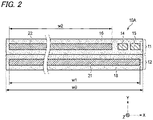
- FIG. 2 is a longitudinal cross-sectional view showing a flexible wiring member 10A according to a first modification.
- the flexible wiring member 10A shown in FIG. 2 includes the first layer 11 and the second layer 12 that are disposed in a manner of overlapping with each other in the thickness direction (Y-axis direction) in a similar manner to the flexible wiring member 10 shown in FIG. 1A .
- a power supply ground line 22 and the communication lines 14 and 15 are arranged in a row in the first layer 11 of the flexible wiring member 10A. Peripheries of the power supply ground line 22 and the communication lines 14 and 15 are covered with the insulating sheath 16 made of resin or the like.
- the power supply ground line 22 is made of a metal having good conductivity such as copper, and for example, the power supply ground line 22 is formed to have a wide cross-sectional shape as shown in FIG. 2 . That is, the power supply ground line 22 is made of a metal material having a foil shape or a thin plate shape, or is formed into a thin plate shape formed by stacking metal materials having a foil shape, so that the conductor width w2 is sufficiently large.
- the power supply ground line 22 is used to supply a relatively large power supply current, it is necessary to increase a cross-sectional area of the power supply ground line 22 to reduce a resistance value so as to prevent the occurrence of a voltage drop. In order to improve the flexibility in the thickness direction, it is necessary to reduce a thickness of the power supply ground line 22. Therefore, a cross-sectional shape of the power supply ground line 22 is formed to be wide.
- Configurations of the communication lines 14 and 15 and the insulating sheath 16 in the first layer 11 of the flexible wiring member 10A are the same as those of the flexible wiring member 10 shown in FIG. 1A .
- the second layer 12 of the flexible wiring member 10A is formed by one power supply line 21 and the insulating sheath 18 that covers the periphery of the power supply line 21.
- the power supply line 21 is made of a metal having good conductivity such as copper, and for example, the power supply line 21 is formed to have a wide cross-sectional shape as shown in FIG. 2 . That is, the power supply line 21 is made of a metal material having a foil shape or a thin plate shape, or is formed into a thin plate shape formed by stacking metal materials having a foil shape, so that the conductor width w1 is sufficiently large.
- the conductor width w1 of the power supply line 21 is formed to be slightly larger than the conductor width w2 of the power supply ground line 22.
- a dimension obtained by adding a width for arranging the communication lines 14 and 15 to the conductor width w2 of the power supply ground line 22 matches the conductor width w1. Since an outer side of the power supply line 21 in the width direction is covered with the insulating sheath 18, the cable width w0 is slightly larger than the conductor width w1.
- the insulating sheath 18 of the second layer 12 is made of the same material as the insulating sheath 16 of the first layer 11. That is, the insulating sheath 18 is made of a soft material such as resin having a sufficient withstand voltage against a high voltage of a power supply, and covers peripheries of the power supply line 21 and outer sides of the conductors in the first layer 11 and the flexible wiring member 10A so as to electrically separate the power supply line 21 from the outer sides of the conductors in the first layer 11 and the flexible wiring member 10A, so that the occurrence of an electric shock, a short circuit, an electric leakage, and the like can be prevented.
- a soft material such as resin having a sufficient withstand voltage against a high voltage of a power supply
- a specification is defined such that the power supply line 21 of the second layer 12 is used as a power supply line (normally, a positive electrode) for supplying power and the power supply ground line 22 of the first layer 11 is used for connection to a ground (normally, a negative electrode: a ground) of a power supply, when a user wires and uses the flexible wiring member 10A shown in FIG. 2 .
- a power supply current flows on the power supply line 21 from a device at the power supply side that is connected to one end of the flexible wiring member 10A in the length direction (Z-axis direction) toward a device at a load side that is connected to the other end.
- a current flows on the power supply ground line 22 adjacent to the power supply line 21 in a direction opposite to that on the power supply line 21.
- the two communication lines 14 and 15 can be used as a pair of transmission lines for communication, such as a CAN bus mounted in a vehicle or the like.
- a noise countermeasure is easy to make for a signal transmitted by communication. That is, since there is almost no change in potential of the ground, even when a voltage on the power supply line 21 or the like greatly fluctuates due to noises, a shielding effect of the power supply ground line 22 can be expected so that voltage fluctuation hardly affects the communication lines 14 and 15.
- FIG. 3 is a longitudinal cross-sectional view showing a flexible wiring member 10B according to a second modification.
- two power supply lines 13A and 13B, and the communication lines 14 and 15 are arranged in a line in the first layer 11.
- the communication lines 14 and 15 are disposed in a substantially central portion in the width direction, the power supply line 13A is disposed at a left side of the communication lines 14 and 15, and the power supply line 13B is disposed at a right side of the communication lines 14 and 15.
- the two power supply lines 13A and 13B have a thin and wide cross-sectional shape.
- a conductor width w21 of the power supply line 13A and a conductor width w22 of the power supply line 13B are slightly smaller than half of the conductor width w1 of the power supply line 17.
- the configuration of the flexible wiring member 10B other than the above is the same as that of the flexible wiring member 10 shown in FIG. 1A .
- the two power supply lines 13A and 13B are used in a state of being electrically connected in parallel to the power supply line 17 of the second layer 12.
- Another specification may be defined such that one or both of the two power supply lines 13A and 13B are used as a power supply ground line in a similar manner to the power supply ground line 22 shown in FIG. 2 .
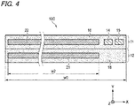
- FIG. 4 is a longitudinal cross-sectional view showing a flexible wiring member 10C according to a third modification.
- the conductor width w2 of the power supply ground line 22 disposed in the first layer 11 and the conductor width w2 of the power supply line 21 disposed in the second layer 12 are formed to have substantially the same dimensions, and the power supply line 21 and the power supply ground line 22 are disposed to have a positional relationship in which the power supply line 21 and the power supply ground line 22 face each other in the thickness direction.
- the communication lines 14 and 15 are disposed at positions adjacent to a right side of the power supply ground line 22 in the width direction.
- the configuration of the flexible wiring member 10C other than the above is the same as that of the flexible wiring member 10A shown in FIG. 2 . Therefore, the cable width w0 of the flexible wiring member 10C is larger than the conductor width w2 of the power supply line 21 and the power supply ground line 22 by an amount of a space in which the communication lines 14 and 15 are arranged.
- FIG. 5 is a longitudinal cross-sectional view showing a flexible wiring member 10D according to a fourth modification.
- the flexible wiring member 10D shown in FIG. 5 can be manufactured, for example, by the following procedure.
- a flexible wiring member (10) capable of electrically connecting a plurality of desired points separated in a length direction (Z-axis direction), the flexible wiring member (10) including
- the power supply line conductor and the communication line conductor are arranged in the wiring member having a structure in which the plurality of conductor holding layers are stacked, the power supply line and the communication line that pass through a common wiring path can be implemented by wiring the single wiring member only. Since the power supply wire conductors having a wide width are disposed in adjacent layers, even when a large cross-sectional area is required to handle a relatively large current, the power supply wire conductors of the respective layers can be made of a thin material, and the flexibility of the entire wiring member in the thickness direction can be increased.
- the plurality of communication line conductors are disposed in only one of the first conductor holding layer and the second conductor holding layer, it is easy to make a noise countermeasure. Since the insulating resin that separates the plurality of conductor holding layers from one another forms a direct coating on the power supply wire conductor, it is easy to reduce the number of components constituting the wiring member and simplify a manufacturing process.
- each of the power supply line conductors may be a high-voltage power supply line conductor.
- the flexible wiring member having the above configuration since the power supply line conductor is formed to be wide, the high-voltage power supply line and the communication line can be easily wired while reducing loss and heat generation due to a voltage drop which is particularly remarkable when the flexible wiring member is connected to a high-voltage power supply or a high-voltage load.
- a width dimension (the conductor width w2) of a first power supply line conductor disposed in the first conductor holding layer together with the communication line conductors may be formed to be smaller than a width dimension (the conductor width w1) of a second power supply line conductor disposed in the second conductor holding layer.
- the flexible wiring member having the above configuration it is possible to prevent the width dimension of the entire wiring member from being excessively increased due to the influence of the communication line conductor.
- a direction of a current flowing through a first power supply line conductor (the power supply line 13) disposed in the first conductor holding layer together with the communication line conductors and a direction of a current flowing through a second power supply line conductor (the power supply line 17) disposed in the second conductor holding layer may be set to be the same.
- both the first power supply line conductor and the second power supply line conductor can be used in a manner of being electrically connected in parallel in order to flow currents in the same direction. Therefore, even when a thin conductor is used, the cross-sectional area of the conductor required for the power supply line to flow a desired current can be easily ensured.
- a direction of a current flowing through a first power supply line conductor (the power supply ground line 22) disposed in the first conductor holding layer together with the communication line conductors and a direction of a current flowing through a second power supply line conductor (the power supply line 21) disposed in the second conductor holding layer may be set to be opposite to each other and the first power supply line conductor is used as a ground line.
- the power supply ground line is provided in the wiring member, even when the flexible wiring member is wired in a vehicle made of resin in which the body ground cannot be used, a path of the ground line can be easily ensured. Since the power supply ground line is provided in the same layer as the communication line conductor, it is easy to make a noise countermeasure.
- the power supply line conductors (the power supply lines 13 and 17) and the communication line conductors (the communication lines 14 and 15) may be made of conductive metals having a foil shape and having the same thickness.
- each conductor is very thin, it is easy to increase the flexibility of the entire wiring member in the thickness direction.
- the flexible wiring member of the present invention it is possible to implement a flexible wiring member that allows energization of a relatively large current, has high flexibility, and is easy to be wired. That is, since the power supply line conductor and the communication line conductor are arranged in the wiring member having a structure in which the plurality of conductor holding layers are stacked, the power supply line and the communication line that pass through a common wiring path can be implemented by wiring the single wiring member only. Since the power supply wire conductors having a wide width are disposed in adjacent layers, even when a large cross-sectional area is required to handle a relatively large current, the power supply wire conductors of the respective layers can be made of a thin material, and the flexibility of the entire wiring member in the thickness direction can be increased.
- the plurality of communication line conductors are disposed in only one of the first conductor holding layer and the second conductor holding layer, it is easy to make a noise countermeasure. Since the insulating resin that separates the plurality of conductor holding layers from one another forms a direct coating on the power supply wire conductor, it is easy to reduce the number of components constituting the wiring member and simplify a manufacturing process.
Landscapes
- Insulated Conductors (AREA)
- Structure Of Printed Boards (AREA)
Abstract
Description
- The present invention relates to a flexible wiring member that can be used for electrically connecting a plurality of devices in a vehicle or the like.
- In a vehicle, a plurality of devices such as electronic control units (ECU) are generally electrically connected to one another using a wiring member configured as a wire harness or the like. In such a case, the wiring member that connects the plurality of devices often includes a wiring member for a power supply line and a wiring member for a communication line. It is assumed that the wiring member for a power supply line and the wiring member for a communication line are wired in a manner of passing through almost the same paths, but these wiring members are normally assembled to a wire harness as independent components.
- On the other hand, for example, Patent Literature 1 discloses a composite cable having sufficient performance as a wire harness. The composite cable includes a cylindrical body, a belt-shaped body having conductivity and extending along an axial direction of the cylindrical body, and an outer cover made of an insulating material that covers the cylindrical body and the belt-shaped body. The outer cover has a flat cross section when cut perpendicularly to the axial direction. The cylindrical body and the belt-shaped body are arranged side by side in a short axis direction of the cross section of the outer cover. The belt-shaped body is arranged such that a longitudinal direction of a cross section of the belt-shaped body when cut perpendicularly to the axial direction is along a long axis direction of the cross section of the outer cover.
- In a composite transmission line disclosed in Patent Literature 2, a plurality of signal transmission lines and a power transmission line are formed as a stacked insulator in which a plurality of insulator layers are stacked, and the composite transmission line includes a first signal transmission line, a second signal transmission line, and the power transmission line. The power transmission line includes power transmission conductor patterns formed along a plurality of layers of the stacked insulator and an interlayer connection conductor that connects the power transmission conductor patterns between layers. A first signal conductor pattern of the first signal transmission line, a second signal conductor pattern of the second signal transmission line, and the power transmission conductor patterns are formed in different layers of the stacked insulator and are formed in parallel to one another. The first signal conductor pattern and the second signal conductor pattern are disposed in a manner of sandwiching a first ground conductor in a stacking direction of the insulator layer, and the power transmission line is disposed at a side portion of the first signal conductor pattern.
- Patent Literature 3 discloses a technique of a flat bus equipped with a wire that can be used for a power supply path and a signal path. In the flat bus equipped with a wire, at least one flat conductor and at least one wire are arranged in parallel and are fixed by an insulating material.
- Patent Literature 4 discloses a flat cable in which a plurality of current conductors and a plurality of data conductors are arranged in substantially the same plane in a manner of being adjacent to one another in a width direction. The plurality of data conductors are disposed between the plurality of current conductors. The cable includes a wavy elbow at a predetermined bending point.
-
- Patent Literature 1:
JP-A-2020-191215 - Patent Literature 2:
WO2016/163436 - Patent Literature 3:
JP-U-6-38118 - Patent Literature 4:
WO01/50482 - When any one of the techniques disclosed in Patent Literatures 1 to 4 is used, a plurality of types of electric wires such as a power supply line and a communication line can be wired together in one cable or the like. Since a current flows in the power supply line is generally larger than a current flows in the communication line, a cross-sectional area of a conductor of the power supply line needs to be increased.
- Therefore, for example, a belt-shaped body 5A (that is, a bus bar) disclosed in Patent Literature 1, a flat conductor 1 disclosed in Patent Literature 3, and a current conductor 1 having a rectangular cross-sectional shape as disclosed in Patent Literature 4 are used. In a case where no very large current flows through the power supply line or in a case where a total length of a line is relatively short, for example, as disclosed in Patent Literature 2, it is also possible to make widths or cross-sectional areas of power transmission conductor patterns 41 to 45 and signal conductor patterns 31 and 32 equal to one another. When it is assumed that a cable length is about several meters, such as a wire harness wired in a vehicle, it is important to sufficiently increase the cross-sectional area of the power supply line to reduce loss and heat generation due to a voltage drop.
- However, when the cross-sectional area of the power supply line is increased in order to flow a large current, rigidity of a corresponding component is increased, and thus resistance to vibration is reduced even when a component having any shape of an electric wire and a bus bar is used. Since bending is difficult when the rigidity is increased, it is difficult to absorb tolerance in a wiring member, and workability of wiring a wire harness in a vehicle is poor.
- Further, even when the power supply line and the communication line are individually wired by independent components, the number of work steps increases. In a case where components having different types of electric wires or different cross-sectional areas are selectively used for each path in accordance with a current value to be handled, since the number of parts of a cable increases, component costs may increase and work efficiency may be low.
- The present invention has been made in view of the above circumstances, and an object of the present invention is to provide a flexible wiring member that has high flexibility and is easy to be wired while allowing energization of a relatively large current.
- According to an embodiment, a flexible wiring member is capable of electrically connecting a plurality of desired points separated in a length direction. The flexible wiring member comprises:
- a plurality of conductor holding layers that are formed in a state of being stacked in a thickness direction and being electrically insulated from one another;
- power supply line conductors that have a wide width and are respectively disposed in both of a first conductor holding layer and a second conductor holding layer that are adjacent to each other in the thickness direction; and
- a plurality of communication line conductors that have a width smaller than that of the power supply line conductors and are disposed in one of the first conductor holding layer and the second conductor holding layer,
- wherein the plurality of conductor holding layers are formed by an insulating resin, and directly cover the power supply line conductors and the communication line conductors.
-
-
FIG. 1A is a longitudinal cross-sectional view andFIG. 1B is a perspective view both showing a flexible wiring member according to an embodiment of the present invention. -
FIG. 2 is a longitudinal cross-sectional view showing a flexible wiring member according to a first modification. -
FIG. 3 is a longitudinal cross-sectional view showing a flexible wiring member according to a second modification. -
FIG. 4 is a longitudinal cross-sectional view showing a flexible wiring member according to a third modification. -
FIG. 5 is a longitudinal cross-sectional view showing a flexible wiring member according to a fourth modification. - A specific embodiment of the present invention will be described below with reference to the drawings.
-
FIG. 1A is a longitudinal cross-sectional view andFIG. 1B is a perspective view both showing aflexible wiring member 10 according to an embodiment of the present invention. - In
FIGS. 1A and 1B , an X axis, a Y axis, and a Z axis respectively correspond to a width direction, a thickness direction, and a length direction of theflexible wiring member 10. - As shown in
FIGS. 1A and 1B , theflexible wiring member 10 has a structure suitable for mounting in a vehicle or the like and suitable for being used as a wiring member for a wire harness that electrically connects a plurality of electronic devices (ECU and the like) to one another. Theflexible wiring member 10 can simultaneously connect both a power supply path and a communication path. In recent years, a vehicle such as a hybrid vehicle or an electric vehicle often handles a high-voltage power supply. Accordingly, theflexible wiring member 10 is configured to handle a high-voltage power supply current of, for example, about several hundred volts. - As shown in
FIG. 1B , theflexible wiring member 10 has a thin and wide planar outer shape, and can be used as a long wiring member. Therefore, theflexible wiring member 10 has particularly high flexibility in the thickness direction, and can be easily shaped by being bent or twisted in the thickness direction so as to follow a predetermined wiring path having a complicated shape in a vehicle or the like. As a result, tolerance can be easily absorbed. - As shown in
FIG. 1A , across section 10a of theflexible wiring member 10 includes afirst layer 11 disposed at an upper side in the thickness direction (Y-axis direction) and asecond layer 12 disposed at a lower side in the thickness direction, and thefirst layer 11 and thesecond layer 12 are stacked. Although a case of a two-layer structure is described as an example inFIG. 1A , the number of layers may be three or more. - In the
flexible wiring member 10, thefirst layer 11 includes onepower supply line 13 and twocommunication lines power supply line 13 and thecommunication lines power supply line 13 and thecommunication lines sheath 16 made of resin or the like. - The
power supply line 13 is made of a metal having good conductivity such as copper, and for example, thepower supply line 13 is formed to have a wide cross-sectional shape as shown inFIG. 1A . That is, thepower supply line 13 is made of a metal material having a foil shape or a thin plate shape, or is formed into a thin plate shape formed by stacking metal materials having a foil shape, so that a conductor width w2 is sufficiently large. - Since the
power supply line 13 is used to supply a relatively large power supply current, it is necessary to increase a cross-sectional area of thepower supply line 13 to reduce a resistance value so as to prevent the occurrence of a voltage drop. In order to improve the flexibility in the thickness direction, it is necessary to reduce a thickness of thepower supply line 13. Therefore, a cross-sectional shape of thepower supply line 13 is formed to be wide. That is, the conductor width w2 is set to a large value by an amount at which a height (thickness) of thepower supply line 13 is smaller than an electric wire in the related art, so that a cross-sectional area of thepower supply line 13 is equal to a cross-sectional area of the electric wire in the related art having the same conductivity when the electric wire in the related art is used as thepower supply line 13, while ensuring the flexibility of thepower supply line 13 in the thickness direction. Therefore, the term "wide" refers to a dimension that can satisfy such a condition. The same applies to widths of other power supply lines and power supply ground lines in the present specification. - Since the
communication lines communication lines communication lines power supply lines 13 and apower supply line 17. - The insulating
sheath 16 is made of a soft material such as resin having a sufficient withstand voltage against a high voltage of a power supply, and covers peripheries of thepower supply line 13 and thecommunication lines power supply line 13 and thecommunication lines second layer 12 or an outer side of theflexible wiring member 10 from thepower supply line 13 and thecommunication lines - Since the
communication lines communication line 14 and thecommunication line 15 can be made relatively small. On the other hand, since thepower supply line 13 handles a high voltage, thepower supply line 13 and thecommunication lines - On the other hand, the
second layer 12 includes onepower supply line 17 and an insulatingsheath 18 that covers the periphery of thepower supply line 17. Thepower supply line 17 is made of a metal having good conductivity such as copper, and is formed to have a wide cross-sectional shape as shown inFIG. 1A . That is, thepower supply line 17 is made of a metal material having a foil shape or a thin plate shape, or is formed into a thin plate shape formed by stacking metal materials having a foil shape, so that a conductor width w1 is sufficiently large. - The conductor width w1 of the
power supply line 17 is formed to be slightly larger than the conductor width w2 of thepower supply line 13. A dimension obtained by adding a width for arranging thecommunication lines power supply line 13 matches the conductor width w1. Since an outer side of thepower supply line 17 in the width direction is covered with the insulatingsheath 18, a cable width w0 is slightly larger than the conductor width w1. - The insulating
sheath 18 of thesecond layer 12 is made of the same material as the insulatingsheath 16 of thefirst layer 11. That is, the insulatingsheath 18 is made of a soft material such as resin having a sufficient withstand voltage against a high voltage of a power supply, and covers peripheries of thepower supply line 17 and an outer side of thefirst layer 11 or theflexible wiring member 10 so as to electrically separate thepower supply line 17 from the outer side of thefirst layer 11 or theflexible wiring member 10, so that the occurrence of an electric shock, a short circuit, an electric leakage, and the like can be prevented. - In the present embodiment, a specification is defined so that the
power supply lines flexible wiring member 10 shown inFIG. 1A is wired and used by a user. It is assumed that a power supply ground wire is separately prepared by using a body ground of a vehicle or the like. Therefore, theflexible wiring member 10 according to the present embodiment is used in a state in which the twopower supply lines - A power supply current simultaneously flows in the same direction on the
power supply line 13 and thepower supply line 17 from a device at the power supply side that is connected to one end in a length direction (Z-axis direction) of theflexible wiring member 10 toward a device at a load side that is connected to the other end. - As a method of connecting the two
power supply lines power supply line 13 and thepower supply line 17 may be disposed in theflexible wiring member 10 between thefirst layer 11 and thesecond layer 12, the twopower supply lines flexible wiring member 10, or the twopower supply lines flexible wiring member 10. - In this manner, a sufficiently large cross-sectional area can be secured at a portion serving as a path of a power supply current by connecting the
power supply lines power supply lines power supply lines - Since the two
power supply lines power supply lines flexible wiring member 10. - On the other hand, the two
communication lines FIG. 1A , since the twocommunication lines first layer 11, that is, in the same layer, the twocommunication lines - The
flexible wiring member 10 shown inFIGS. 1A and 1B can be manufactured by, for example, the following procedure when a general extrusion molding technique is used. - (1) Long-length
power supply lines communication lines - (2) In order to form the
first layer 11, thepower supply line 13 and thecommunication lines sheath 16 is formed of a molten resin in a manner of covering outer sides of all of the core wires when passing through the extruder. The insulatingsheath 16 in a molten state is cooled in a water tank or the like to mold thefirst layer 11. - (3) In order to form the
second layer 12, thepower supply line 17 serving as a core wire is disposed in a path passing through the extruder, and the core wire is gradually pulled from the tip end side. The insulatingsheath 18 is formed in a manner of covering an outer side of thepower supply line 17 that is all core wires when passing through the extruder. The insulatingsheath 18 in a molten state is cooled in a water tank or the like to mold thesecond layer 12. - (4) The molded
first layer 11 and the moldedsecond layer 12 are stacked and bonded in the thickness direction, and are molded into a state of theflexible wiring member 10 in which thefirst layer 11 and thesecond layer 12 are integrated. - As will be described later, the
first layer 11 and thesecond layer 12 may be simultaneously molded in one step. - A plurality of flexible printed circuits (FPC) may be stacked and integrated in the thickness direction to manufacture the
flexible wiring member 10 having the same configuration as described above. In this case, an outer side of theflexible wiring member 10 is covered with an insulating sheath so that a conductor is not exposed to the outer side. - As described above, in the
flexible wiring member 10 according to the embodiment of the present invention, since the thickness of each of thepower supply lines power supply lines flexible wiring member 10 can be easily wired along wiring paths having various shapes. Since flexibility is high, durability against vibration is high, tolerance can be absorbed, and automatic assembly of a wire harness can be handled. - Since the
power supply lines communication lines flexible wiring member 10 only in order to electrically connect a plurality of devices such as various ECUs. Therefore, the structure can be simplified and work efficiency can be improved. - In particular, since the specification is defined such that the
power supply lines power supply lines flexible wiring member 10, and a resistance value can be sufficiently reduced. - As shown in
FIG. 1A , since the conductor width w2 of thepower supply line 13 of thefirst layer 11 is formed to be smaller than the conductor width w1 of thepower supply line 17 of thesecond layer 12, an arrangement space of thecommunication lines first layer 11. Therefore, it is possible to prevent the cable width w0 from increasing more than necessary. -
FIG. 2 is a longitudinal cross-sectional view showing aflexible wiring member 10A according to a first modification. - The
flexible wiring member 10A shown inFIG. 2 includes thefirst layer 11 and thesecond layer 12 that are disposed in a manner of overlapping with each other in the thickness direction (Y-axis direction) in a similar manner to theflexible wiring member 10 shown inFIG. 1A . - A power
supply ground line 22 and thecommunication lines first layer 11 of theflexible wiring member 10A. Peripheries of the powersupply ground line 22 and thecommunication lines sheath 16 made of resin or the like. - The power
supply ground line 22 is made of a metal having good conductivity such as copper, and for example, the powersupply ground line 22 is formed to have a wide cross-sectional shape as shown inFIG. 2 . That is, the powersupply ground line 22 is made of a metal material having a foil shape or a thin plate shape, or is formed into a thin plate shape formed by stacking metal materials having a foil shape, so that the conductor width w2 is sufficiently large. - Since the power
supply ground line 22 is used to supply a relatively large power supply current, it is necessary to increase a cross-sectional area of the powersupply ground line 22 to reduce a resistance value so as to prevent the occurrence of a voltage drop. In order to improve the flexibility in the thickness direction, it is necessary to reduce a thickness of the powersupply ground line 22. Therefore, a cross-sectional shape of the powersupply ground line 22 is formed to be wide. - Configurations of the
communication lines sheath 16 in thefirst layer 11 of theflexible wiring member 10A are the same as those of theflexible wiring member 10 shown inFIG. 1A . - On the other hand, the
second layer 12 of theflexible wiring member 10A is formed by onepower supply line 21 and the insulatingsheath 18 that covers the periphery of thepower supply line 21. Thepower supply line 21 is made of a metal having good conductivity such as copper, and for example, thepower supply line 21 is formed to have a wide cross-sectional shape as shown inFIG. 2 . That is, thepower supply line 21 is made of a metal material having a foil shape or a thin plate shape, or is formed into a thin plate shape formed by stacking metal materials having a foil shape, so that the conductor width w1 is sufficiently large. - The conductor width w1 of the
power supply line 21 is formed to be slightly larger than the conductor width w2 of the powersupply ground line 22. A dimension obtained by adding a width for arranging thecommunication lines supply ground line 22 matches the conductor width w1. Since an outer side of thepower supply line 21 in the width direction is covered with the insulatingsheath 18, the cable width w0 is slightly larger than the conductor width w1. - The insulating
sheath 18 of thesecond layer 12 is made of the same material as the insulatingsheath 16 of thefirst layer 11. That is, the insulatingsheath 18 is made of a soft material such as resin having a sufficient withstand voltage against a high voltage of a power supply, and covers peripheries of thepower supply line 21 and outer sides of the conductors in thefirst layer 11 and theflexible wiring member 10A so as to electrically separate thepower supply line 21 from the outer sides of the conductors in thefirst layer 11 and theflexible wiring member 10A, so that the occurrence of an electric shock, a short circuit, an electric leakage, and the like can be prevented. - In the present embodiment, a specification is defined such that the
power supply line 21 of thesecond layer 12 is used as a power supply line (normally, a positive electrode) for supplying power and the powersupply ground line 22 of thefirst layer 11 is used for connection to a ground (normally, a negative electrode: a ground) of a power supply, when a user wires and uses theflexible wiring member 10A shown inFIG. 2 . - Therefore, a power supply current flows on the
power supply line 21 from a device at the power supply side that is connected to one end of theflexible wiring member 10A in the length direction (Z-axis direction) toward a device at a load side that is connected to the other end. A current flows on the powersupply ground line 22 adjacent to thepower supply line 21 in a direction opposite to that on thepower supply line 21. - On the other hand, the two
communication lines flexible wiring member 10A shown inFIG. 2 , since the powersupply ground line 22 is arranged at a position adjacent to the twocommunication lines first layer 11 as the twocommunication lines power supply line 21 or the like greatly fluctuates due to noises, a shielding effect of the powersupply ground line 22 can be expected so that voltage fluctuation hardly affects thecommunication lines -
FIG. 3 is a longitudinal cross-sectional view showing aflexible wiring member 10B according to a second modification. - In the
flexible wiring member 10B shown inFIG. 3 , twopower supply lines communication lines first layer 11. The communication lines 14 and 15 are disposed in a substantially central portion in the width direction, thepower supply line 13A is disposed at a left side of thecommunication lines power supply line 13B is disposed at a right side of thecommunication lines - The two
power supply lines power supply line 13A and a conductor width w22 of thepower supply line 13B are slightly smaller than half of the conductor width w1 of thepower supply line 17. - The configuration of the
flexible wiring member 10B other than the above is the same as that of theflexible wiring member 10 shown inFIG. 1A . - In the
flexible wiring member 10B, it is assumed that a specification is defined such that the twopower supply lines power supply line 17 of thesecond layer 12. Another specification may be defined such that one or both of the twopower supply lines supply ground line 22 shown inFIG. 2 . -
FIG. 4 is a longitudinal cross-sectional view showing aflexible wiring member 10C according to a third modification. - In the
flexible wiring member 10C shown inFIG. 4 , the conductor width w2 of the powersupply ground line 22 disposed in thefirst layer 11 and the conductor width w2 of thepower supply line 21 disposed in thesecond layer 12 are formed to have substantially the same dimensions, and thepower supply line 21 and the powersupply ground line 22 are disposed to have a positional relationship in which thepower supply line 21 and the powersupply ground line 22 face each other in the thickness direction. The communication lines 14 and 15 are disposed at positions adjacent to a right side of the powersupply ground line 22 in the width direction. - The configuration of the
flexible wiring member 10C other than the above is the same as that of theflexible wiring member 10A shown inFIG. 2 . Therefore, the cable width w0 of theflexible wiring member 10C is larger than the conductor width w2 of thepower supply line 21 and the powersupply ground line 22 by an amount of a space in which thecommunication lines -
FIG. 5 is a longitudinal cross-sectional view showing aflexible wiring member 10D according to a fourth modification. - In the
flexible wiring member 10D shown inFIG. 5 , there is no boundary between thefirst layer 11 and thesecond layer 12. That is, when thefirst layer 11 and thesecond layer 12 are molded together by one extrusion molding, the boundary between thefirst layer 11 and thesecond layer 12 is eliminated as in theflexible wiring member 10D shown inFIG. 5 . - The
flexible wiring member 10D shown inFIG. 5 can be manufactured, for example, by the following procedure. - (1) Long-length
power supply lines communication lines - (2) In order to form the
first layer 11 and thesecond layer 12, thepower supply line 13 and thecommunication lines power supply line 17 is arranged below thepower supply line 13 and thecommunication lines sheath 16 is formed of a molten resin in a manner of covering outer sides of all of the core wires when passing through the extruder. The insulatingsheath 16 in a molten state is cooled in a water tank or the like to mold thefirst layer 11 and thesecond layer 12. As a result, thefirst layer 11 and thesecond layer 12 are simultaneously molded and the entireflexible wiring member 10D is molded. - According to an embodiment, there is provided a flexible wiring member (10) capable of electrically connecting a plurality of desired points separated in a length direction (Z-axis direction), the flexible wiring member (10) including
- a plurality of conductor holding layers (the
first layer 11 and the second layer 12) that are formed in a state of being stacked in a thickness direction and being electrically insulated from one another; - power supply line conductors (the
power supply lines 13 and 17) that have a wide width and are respectively disposed in both of a first conductor holding layer (the first layer 11) and a second conductor holding layer (the second layer 12) that are adjacent to each other in the thickness direction; and - a plurality of communication line conductors (the
communication lines 14 and 15) that have a width smaller than that of the power supply line conductors and are disposed in one of the first conductor holding layer and the second conductor holding layer, - in which the plurality of conductor holding layers are formed by an insulating resin (the insulating
sheaths 16 and 18), and directly cover the power supply line conductors and the communication line conductors. - According to the flexible wiring member having the above configuration, since the power supply line conductor and the communication line conductor are arranged in the wiring member having a structure in which the plurality of conductor holding layers are stacked, the power supply line and the communication line that pass through a common wiring path can be implemented by wiring the single wiring member only. Since the power supply wire conductors having a wide width are disposed in adjacent layers, even when a large cross-sectional area is required to handle a relatively large current, the power supply wire conductors of the respective layers can be made of a thin material, and the flexibility of the entire wiring member in the thickness direction can be increased. Since the plurality of communication line conductors are disposed in only one of the first conductor holding layer and the second conductor holding layer, it is easy to make a noise countermeasure. Since the insulating resin that separates the plurality of conductor holding layers from one another forms a direct coating on the power supply wire conductor, it is easy to reduce the number of components constituting the wiring member and simplify a manufacturing process.
- In the flexible wiring member, each of the power supply line conductors may be a high-voltage power supply line conductor.
- According to the flexible wiring member having the above configuration, since the power supply line conductor is formed to be wide, the high-voltage power supply line and the communication line can be easily wired while reducing loss and heat generation due to a voltage drop which is particularly remarkable when the flexible wiring member is connected to a high-voltage power supply or a high-voltage load.
- In the flexible wiring member, a width dimension (the conductor width w2) of a first power supply line conductor disposed in the first conductor holding layer together with the communication line conductors may be formed to be smaller than a width dimension (the conductor width w1) of a second power supply line conductor disposed in the second conductor holding layer.
- According to the flexible wiring member having the above configuration, it is possible to prevent the width dimension of the entire wiring member from being excessively increased due to the influence of the communication line conductor.
- In the flexible wiring member, usage restrictions may be made in which a direction of a current flowing through a first power supply line conductor (the power supply line 13) disposed in the first conductor holding layer together with the communication line conductors and a direction of a current flowing through a second power supply line conductor (the power supply line 17) disposed in the second conductor holding layer may be set to be the same.
- According to the flexible wiring member having the above configuration, both the first power supply line conductor and the second power supply line conductor can be used in a manner of being electrically connected in parallel in order to flow currents in the same direction. Therefore, even when a thin conductor is used, the cross-sectional area of the conductor required for the power supply line to flow a desired current can be easily ensured.
- In the flexible wiring member, usage restrictions may be made in which a direction of a current flowing through a first power supply line conductor (the power supply ground line 22) disposed in the first conductor holding layer together with the communication line conductors and a direction of a current flowing through a second power supply line conductor (the power supply line 21) disposed in the second conductor holding layer may be set to be opposite to each other and the first power supply line conductor is used as a ground line.
- According to the flexible wiring member having the above configuration, since the power supply ground line is provided in the wiring member, even when the flexible wiring member is wired in a vehicle made of resin in which the body ground cannot be used, a path of the ground line can be easily ensured. Since the power supply ground line is provided in the same layer as the communication line conductor, it is easy to make a noise countermeasure.
- In the flexible wiring member, the power supply line conductors (the
power supply lines 13 and 17) and the communication line conductors (thecommunication lines 14 and 15) may be made of conductive metals having a foil shape and having the same thickness. - According to the flexible wiring member having the above configuration, since each conductor is very thin, it is easy to increase the flexibility of the entire wiring member in the thickness direction.
- According to the flexible wiring member of the present invention, it is possible to implement a flexible wiring member that allows energization of a relatively large current, has high flexibility, and is easy to be wired. That is, since the power supply line conductor and the communication line conductor are arranged in the wiring member having a structure in which the plurality of conductor holding layers are stacked, the power supply line and the communication line that pass through a common wiring path can be implemented by wiring the single wiring member only. Since the power supply wire conductors having a wide width are disposed in adjacent layers, even when a large cross-sectional area is required to handle a relatively large current, the power supply wire conductors of the respective layers can be made of a thin material, and the flexibility of the entire wiring member in the thickness direction can be increased. Since the plurality of communication line conductors are disposed in only one of the first conductor holding layer and the second conductor holding layer, it is easy to make a noise countermeasure. Since the insulating resin that separates the plurality of conductor holding layers from one another forms a direct coating on the power supply wire conductor, it is easy to reduce the number of components constituting the wiring member and simplify a manufacturing process.
Claims (6)
- A flexible wiring member capable of electrically connecting a plurality of desired points separated in a length direction, the flexible wiring member comprising:a plurality of conductor holding layers that are formed in a state of being stacked in a thickness direction and being electrically insulated from one another;power supply line conductors that have a wide width and are respectively disposed in both of a first conductor holding layer and a second conductor holding layer that are adjacent to each other in the thickness direction; anda plurality of communication line conductors that have a width smaller than that of the power supply line conductors and are disposed in one of the first conductor holding layer and the second conductor holding layer,wherein the plurality of conductor holding layers are formed by an insulating resin, and directly cover the power supply line conductors and the communication line conductors.
- The flexible wiring member according to claim 1,
wherein each of the power supply line conductors is a high-voltage power supply line conductor. - The flexible wiring member according to claim 1 or 2,
wherein a width dimension of a first power supply line conductor disposed in the first conductor holding layer together with the communication line conductors is formed to be smaller than a width dimension of a second power supply line conductor disposed in the second conductor holding layer. - The flexible wiring member according to claim 1 or 2,
wherein usage restrictions are made in which a direction of a current flowing through a first power supply line conductor disposed in the first conductor holding layer together with the communication line conductors and a direction of a current flowing through a second power supply line conductor disposed in the second conductor holding layer are set to be the same. - The flexible wiring member according to claim 1 or 2,
wherein usage restrictions are made in which a direction of a current flowing through a first power supply line conductor disposed in the first conductor holding layer together with the communication line conductors and a direction of a current flowing through a second power supply line conductor disposed in the second conductor holding layer are set to be opposite to each other and the first power supply line conductor is used as a ground line. - The flexible wiring member according to any one of claims 1 to 5,
wherein the power supply line conductors and the communication line conductors are made of conductive metals having a foil shape and having the same thickness.
Applications Claiming Priority (1)
| Application Number | Priority Date | Filing Date | Title |
|---|---|---|---|
| JP2021000949A JP7227281B2 (en) | 2021-01-06 | 2021-01-06 | Flexible wiring material |
Publications (2)
| Publication Number | Publication Date |
|---|---|
| EP4027354A1 true EP4027354A1 (en) | 2022-07-13 |
| EP4027354B1 EP4027354B1 (en) | 2023-07-05 |
Family
ID=79185528
Family Applications (1)
| Application Number | Title | Priority Date | Filing Date |
|---|---|---|---|
| EP21218304.0A Active EP4027354B1 (en) | 2021-01-06 | 2021-12-30 | Flexible wiring member |
Country Status (4)
| Country | Link |
|---|---|
| US (1) | US11990256B2 (en) |
| EP (1) | EP4027354B1 (en) |
| JP (1) | JP7227281B2 (en) |
| CN (1) | CN114724749B (en) |
Families Citing this family (1)
| Publication number | Priority date | Publication date | Assignee | Title |
|---|---|---|---|---|
| EP3412513B1 (en) * | 2017-06-07 | 2019-08-14 | Grupo Antolin-Ingenieria, S.A. | Interior trim for vehicles with electrical conductors and method for manufacturing same |
Citations (5)
| Publication number | Priority date | Publication date | Assignee | Title |
|---|---|---|---|---|
| JPH0638118U (en) | 1992-10-21 | 1994-05-20 | 日本メクトロン株式会社 | Flat type bus bar with wire |
| WO2016163436A1 (en) | 2015-04-09 | 2016-10-13 | 株式会社村田製作所 | Combined transmission line, and electronic device |
| WO2019093309A1 (en) * | 2017-11-08 | 2019-05-16 | 株式会社オートネットワーク技術研究所 | Electric wire conductor, covered electric wire, and wire harness |
| US20200324718A1 (en) * | 2019-04-12 | 2020-10-15 | Aptiv Technologies Limited | Wiring harness assembly |
| JP2020191215A (en) | 2019-05-21 | 2020-11-26 | 古河電気工業株式会社 | Composite cable, wire harness routing structure, and method of manufacturing composite cable |
Family Cites Families (10)
| Publication number | Priority date | Publication date | Assignee | Title |
|---|---|---|---|---|
| US3459879A (en) * | 1967-05-29 | 1969-08-05 | Hughes Aircraft Co | Flexible multiflat conductor characteristic impedance cable |
| US4490690A (en) * | 1982-04-22 | 1984-12-25 | Junkosha Company, Ltd. | Strip line cable |
| US4707671A (en) * | 1985-05-31 | 1987-11-17 | Junkosha Co., Ltd. | Electrical transmission line |
| US4801764A (en) * | 1986-02-11 | 1989-01-31 | Cooper Industries, Inc. | Cable assembly for use under carpeting |
| FR2784635B1 (en) * | 1998-10-15 | 2000-12-29 | Framatome Connectors Int | WIRING DEVICE FOR MOTOR VEHICLES OR THE LIKE |
| FI107650B (en) | 2000-01-04 | 2001-09-14 | Iws Int Oy | The flat cable |
| JP5284308B2 (en) | 2010-04-19 | 2013-09-11 | 日本メクトロン株式会社 | Flexible circuit board and manufacturing method thereof |
| JP6423930B1 (en) | 2017-07-28 | 2018-11-14 | Smk株式会社 | Photoelectric composite cable |
| JP2019096546A (en) | 2017-11-27 | 2019-06-20 | トヨタ自動車株式会社 | Flat type wiring structure |
| JP2019192487A (en) * | 2018-04-25 | 2019-10-31 | 矢崎総業株式会社 | Wire harness |
-
2021
- 2021-01-06 JP JP2021000949A patent/JP7227281B2/en active Active
- 2021-12-30 EP EP21218304.0A patent/EP4027354B1/en active Active
-
2022
- 2022-01-05 US US17/568,973 patent/US11990256B2/en active Active
- 2022-01-06 CN CN202210008752.7A patent/CN114724749B/en active Active
Patent Citations (5)
| Publication number | Priority date | Publication date | Assignee | Title |
|---|---|---|---|---|
| JPH0638118U (en) | 1992-10-21 | 1994-05-20 | 日本メクトロン株式会社 | Flat type bus bar with wire |
| WO2016163436A1 (en) | 2015-04-09 | 2016-10-13 | 株式会社村田製作所 | Combined transmission line, and electronic device |
| WO2019093309A1 (en) * | 2017-11-08 | 2019-05-16 | 株式会社オートネットワーク技術研究所 | Electric wire conductor, covered electric wire, and wire harness |
| US20200324718A1 (en) * | 2019-04-12 | 2020-10-15 | Aptiv Technologies Limited | Wiring harness assembly |
| JP2020191215A (en) | 2019-05-21 | 2020-11-26 | 古河電気工業株式会社 | Composite cable, wire harness routing structure, and method of manufacturing composite cable |
Also Published As
| Publication number | Publication date |
|---|---|
| JP2022106157A (en) | 2022-07-19 |
| US11990256B2 (en) | 2024-05-21 |
| CN114724749B (en) | 2024-06-21 |
| EP4027354B1 (en) | 2023-07-05 |
| US20220215982A1 (en) | 2022-07-07 |
| CN114724749A (en) | 2022-07-08 |
| JP7227281B2 (en) | 2023-02-21 |
Similar Documents
| Publication | Publication Date | Title |
|---|---|---|
| CN109415027B (en) | Vehicle circuit body | |
| JP6002985B2 (en) | Intermediate member for wire harness and wire harness | |
| JP5986812B2 (en) | Wire harness | |
| EP2666169B1 (en) | High-voltage conductive path and wiring harness | |
| JP2014035964A (en) | Multilayer coaxial electric wire | |
| JP5884970B2 (en) | Wire harness manufacturing method and manufacturing wiring method | |
| CN109285633B (en) | Method for producing a busbar by means of a metal core and busbar | |
| EP4027354B1 (en) | Flexible wiring member | |
| US20180301246A1 (en) | Wiring member and method of manufacturing wiring member | |
| JP7557183B2 (en) | Flat conductor cable connection terminal structure | |
| CN115376724A (en) | Wire Harness Components | |
| US20240212880A1 (en) | Flexible flat wire cable with high frequency conductors | |
| CN220138704U (en) | an electrical connection device | |
| US20250136024A1 (en) | Wire harness | |
| CN109661329B (en) | Vehicle circuit body | |
| JP7733070B2 (en) | Wire harness | |
| US20110280526A1 (en) | Electrical Cable Having Return Wires Positioned Between Force Wires | |
| US20240147632A1 (en) | Wiring board | |
| JPS6180712A (en) | Concentrated circuit boards for wire harnesses and automotive wire harnesses | |
| CN120513695A (en) | High current printed electronic cable harness connection | |
| JP2009231011A (en) | Electric wire shielding structure | |
| JP2025138074A (en) | Floor harness | |
| CN117199862A (en) | Vehicle wiring harness connection device, connection method and vehicle | |
| CN121358639A (en) | Media modules for motor vehicles, layout structures for motor vehicles, and motor vehicles | |
| WO2016129380A1 (en) | Vehicle ground wiring structure |
Legal Events
| Date | Code | Title | Description |
|---|---|---|---|
| PUAI | Public reference made under article 153(3) epc to a published international application that has entered the european phase |
Free format text: ORIGINAL CODE: 0009012 |
|
| STAA | Information on the status of an ep patent application or granted ep patent |
Free format text: STATUS: REQUEST FOR EXAMINATION WAS MADE |
|
| 17P | Request for examination filed |
Effective date: 20211230 |
|
| AK | Designated contracting states |
Kind code of ref document: A1 Designated state(s): AL AT BE BG CH CY CZ DE DK EE ES FI FR GB GR HR HU IE IS IT LI LT LU LV MC MK MT NL NO PL PT RO RS SE SI SK SM TR |
|
| STAA | Information on the status of an ep patent application or granted ep patent |
Free format text: STATUS: EXAMINATION IS IN PROGRESS |
|
| 17Q | First examination report despatched |
Effective date: 20220901 |
|
| GRAP | Despatch of communication of intention to grant a patent |
Free format text: ORIGINAL CODE: EPIDOSNIGR1 |
|
| STAA | Information on the status of an ep patent application or granted ep patent |
Free format text: STATUS: GRANT OF PATENT IS INTENDED |
|
| INTG | Intention to grant announced |
Effective date: 20230412 |
|
| GRAS | Grant fee paid |
Free format text: ORIGINAL CODE: EPIDOSNIGR3 |
|
| RAP3 | Party data changed (applicant data changed or rights of an application transferred) |
Owner name: YAZAKI CORPORATION |
|
| GRAA | (expected) grant |
Free format text: ORIGINAL CODE: 0009210 |
|
| STAA | Information on the status of an ep patent application or granted ep patent |
Free format text: STATUS: THE PATENT HAS BEEN GRANTED |
|
| AK | Designated contracting states |
Kind code of ref document: B1 Designated state(s): AL AT BE BG CH CY CZ DE DK EE ES FI FR GB GR HR HU IE IS IT LI LT LU LV MC MK MT NL NO PL PT RO RS SE SI SK SM TR |
|
| REG | Reference to a national code |
Ref country code: CH Ref legal event code: EP |
|
| REG | Reference to a national code |
Ref country code: AT Ref legal event code: REF Ref document number: 1585605 Country of ref document: AT Kind code of ref document: T Effective date: 20230715 |
|
| REG | Reference to a national code |
Ref country code: DE Ref legal event code: R096 Ref document number: 602021003290 Country of ref document: DE |
|
| REG | Reference to a national code |
Ref country code: IE Ref legal event code: FG4D |
|
| REG | Reference to a national code |
Ref country code: LT Ref legal event code: MG9D |
|
| REG | Reference to a national code |
Ref country code: NL Ref legal event code: MP Effective date: 20230705 |
|
| REG | Reference to a national code |
Ref country code: AT Ref legal event code: MK05 Ref document number: 1585605 Country of ref document: AT Kind code of ref document: T Effective date: 20230705 |
|
| PG25 | Lapsed in a contracting state [announced via postgrant information from national office to epo] |
Ref country code: NL Free format text: LAPSE BECAUSE OF FAILURE TO SUBMIT A TRANSLATION OF THE DESCRIPTION OR TO PAY THE FEE WITHIN THE PRESCRIBED TIME-LIMIT Effective date: 20230705 |
|
| PG25 | Lapsed in a contracting state [announced via postgrant information from national office to epo] |
Ref country code: GR Free format text: LAPSE BECAUSE OF FAILURE TO SUBMIT A TRANSLATION OF THE DESCRIPTION OR TO PAY THE FEE WITHIN THE PRESCRIBED TIME-LIMIT Effective date: 20231006 |
|
| PG25 | Lapsed in a contracting state [announced via postgrant information from national office to epo] |
Ref country code: ES Free format text: LAPSE BECAUSE OF FAILURE TO SUBMIT A TRANSLATION OF THE DESCRIPTION OR TO PAY THE FEE WITHIN THE PRESCRIBED TIME-LIMIT Effective date: 20230705 |
|
| PG25 | Lapsed in a contracting state [announced via postgrant information from national office to epo] |
Ref country code: IS Free format text: LAPSE BECAUSE OF FAILURE TO SUBMIT A TRANSLATION OF THE DESCRIPTION OR TO PAY THE FEE WITHIN THE PRESCRIBED TIME-LIMIT Effective date: 20231105 |
|
| PG25 | Lapsed in a contracting state [announced via postgrant information from national office to epo] |
Ref country code: SE Free format text: LAPSE BECAUSE OF FAILURE TO SUBMIT A TRANSLATION OF THE DESCRIPTION OR TO PAY THE FEE WITHIN THE PRESCRIBED TIME-LIMIT Effective date: 20230705 Ref country code: RS Free format text: LAPSE BECAUSE OF FAILURE TO SUBMIT A TRANSLATION OF THE DESCRIPTION OR TO PAY THE FEE WITHIN THE PRESCRIBED TIME-LIMIT Effective date: 20230705 Ref country code: PT Free format text: LAPSE BECAUSE OF FAILURE TO SUBMIT A TRANSLATION OF THE DESCRIPTION OR TO PAY THE FEE WITHIN THE PRESCRIBED TIME-LIMIT Effective date: 20231106 Ref country code: NO Free format text: LAPSE BECAUSE OF FAILURE TO SUBMIT A TRANSLATION OF THE DESCRIPTION OR TO PAY THE FEE WITHIN THE PRESCRIBED TIME-LIMIT Effective date: 20231005 Ref country code: LV Free format text: LAPSE BECAUSE OF FAILURE TO SUBMIT A TRANSLATION OF THE DESCRIPTION OR TO PAY THE FEE WITHIN THE PRESCRIBED TIME-LIMIT Effective date: 20230705 Ref country code: LT Free format text: LAPSE BECAUSE OF FAILURE TO SUBMIT A TRANSLATION OF THE DESCRIPTION OR TO PAY THE FEE WITHIN THE PRESCRIBED TIME-LIMIT Effective date: 20230705 Ref country code: IS Free format text: LAPSE BECAUSE OF FAILURE TO SUBMIT A TRANSLATION OF THE DESCRIPTION OR TO PAY THE FEE WITHIN THE PRESCRIBED TIME-LIMIT Effective date: 20231105 Ref country code: HR Free format text: LAPSE BECAUSE OF FAILURE TO SUBMIT A TRANSLATION OF THE DESCRIPTION OR TO PAY THE FEE WITHIN THE PRESCRIBED TIME-LIMIT Effective date: 20230705 Ref country code: GR Free format text: LAPSE BECAUSE OF FAILURE TO SUBMIT A TRANSLATION OF THE DESCRIPTION OR TO PAY THE FEE WITHIN THE PRESCRIBED TIME-LIMIT Effective date: 20231006 Ref country code: FI Free format text: LAPSE BECAUSE OF FAILURE TO SUBMIT A TRANSLATION OF THE DESCRIPTION OR TO PAY THE FEE WITHIN THE PRESCRIBED TIME-LIMIT Effective date: 20230705 Ref country code: ES Free format text: LAPSE BECAUSE OF FAILURE TO SUBMIT A TRANSLATION OF THE DESCRIPTION OR TO PAY THE FEE WITHIN THE PRESCRIBED TIME-LIMIT Effective date: 20230705 Ref country code: AT Free format text: LAPSE BECAUSE OF FAILURE TO SUBMIT A TRANSLATION OF THE DESCRIPTION OR TO PAY THE FEE WITHIN THE PRESCRIBED TIME-LIMIT Effective date: 20230705 |
|
| PG25 | Lapsed in a contracting state [announced via postgrant information from national office to epo] |
Ref country code: PL Free format text: LAPSE BECAUSE OF FAILURE TO SUBMIT A TRANSLATION OF THE DESCRIPTION OR TO PAY THE FEE WITHIN THE PRESCRIBED TIME-LIMIT Effective date: 20230705 |
|
| REG | Reference to a national code |
Ref country code: DE Ref legal event code: R097 Ref document number: 602021003290 Country of ref document: DE |
|
| PG25 | Lapsed in a contracting state [announced via postgrant information from national office to epo] |
Ref country code: SM Free format text: LAPSE BECAUSE OF FAILURE TO SUBMIT A TRANSLATION OF THE DESCRIPTION OR TO PAY THE FEE WITHIN THE PRESCRIBED TIME-LIMIT Effective date: 20230705 Ref country code: RO Free format text: LAPSE BECAUSE OF FAILURE TO SUBMIT A TRANSLATION OF THE DESCRIPTION OR TO PAY THE FEE WITHIN THE PRESCRIBED TIME-LIMIT Effective date: 20230705 Ref country code: EE Free format text: LAPSE BECAUSE OF FAILURE TO SUBMIT A TRANSLATION OF THE DESCRIPTION OR TO PAY THE FEE WITHIN THE PRESCRIBED TIME-LIMIT Effective date: 20230705 Ref country code: DK Free format text: LAPSE BECAUSE OF FAILURE TO SUBMIT A TRANSLATION OF THE DESCRIPTION OR TO PAY THE FEE WITHIN THE PRESCRIBED TIME-LIMIT Effective date: 20230705 Ref country code: CZ Free format text: LAPSE BECAUSE OF FAILURE TO SUBMIT A TRANSLATION OF THE DESCRIPTION OR TO PAY THE FEE WITHIN THE PRESCRIBED TIME-LIMIT Effective date: 20230705 Ref country code: SK Free format text: LAPSE BECAUSE OF FAILURE TO SUBMIT A TRANSLATION OF THE DESCRIPTION OR TO PAY THE FEE WITHIN THE PRESCRIBED TIME-LIMIT Effective date: 20230705 |
|
| PLBE | No opposition filed within time limit |
Free format text: ORIGINAL CODE: 0009261 |
|
| STAA | Information on the status of an ep patent application or granted ep patent |
Free format text: STATUS: NO OPPOSITION FILED WITHIN TIME LIMIT |
|
| PG25 | Lapsed in a contracting state [announced via postgrant information from national office to epo] |
Ref country code: IT Free format text: LAPSE BECAUSE OF FAILURE TO SUBMIT A TRANSLATION OF THE DESCRIPTION OR TO PAY THE FEE WITHIN THE PRESCRIBED TIME-LIMIT Effective date: 20230705 |
|
| 26N | No opposition filed |
Effective date: 20240408 |
|
| PG25 | Lapsed in a contracting state [announced via postgrant information from national office to epo] |
Ref country code: SI Free format text: LAPSE BECAUSE OF FAILURE TO SUBMIT A TRANSLATION OF THE DESCRIPTION OR TO PAY THE FEE WITHIN THE PRESCRIBED TIME-LIMIT Effective date: 20230705 |
|
| PG25 | Lapsed in a contracting state [announced via postgrant information from national office to epo] |
Ref country code: LU Free format text: LAPSE BECAUSE OF NON-PAYMENT OF DUE FEES Effective date: 20231230 |
|
| PG25 | Lapsed in a contracting state [announced via postgrant information from national office to epo] |
Ref country code: MC Free format text: LAPSE BECAUSE OF FAILURE TO SUBMIT A TRANSLATION OF THE DESCRIPTION OR TO PAY THE FEE WITHIN THE PRESCRIBED TIME-LIMIT Effective date: 20230705 |
|
| REG | Reference to a national code |
Ref country code: BE Ref legal event code: MM Effective date: 20231231 |
|
| PG25 | Lapsed in a contracting state [announced via postgrant information from national office to epo] |
Ref country code: MC Free format text: LAPSE BECAUSE OF FAILURE TO SUBMIT A TRANSLATION OF THE DESCRIPTION OR TO PAY THE FEE WITHIN THE PRESCRIBED TIME-LIMIT Effective date: 20230705 Ref country code: LU Free format text: LAPSE BECAUSE OF NON-PAYMENT OF DUE FEES Effective date: 20231230 |
|
| REG | Reference to a national code |
Ref country code: IE Ref legal event code: MM4A |
|
| PG25 | Lapsed in a contracting state [announced via postgrant information from national office to epo] |
Ref country code: IE Free format text: LAPSE BECAUSE OF NON-PAYMENT OF DUE FEES Effective date: 20231230 |
|
| PG25 | Lapsed in a contracting state [announced via postgrant information from national office to epo] |
Ref country code: BE Free format text: LAPSE BECAUSE OF NON-PAYMENT OF DUE FEES Effective date: 20231231 |
|
| PG25 | Lapsed in a contracting state [announced via postgrant information from national office to epo] |
Ref country code: FR Free format text: LAPSE BECAUSE OF NON-PAYMENT OF DUE FEES Effective date: 20231231 |
|
| PG25 | Lapsed in a contracting state [announced via postgrant information from national office to epo] |
Ref country code: IE Free format text: LAPSE BECAUSE OF NON-PAYMENT OF DUE FEES Effective date: 20231230 Ref country code: FR Free format text: LAPSE BECAUSE OF NON-PAYMENT OF DUE FEES Effective date: 20231231 Ref country code: BE Free format text: LAPSE BECAUSE OF NON-PAYMENT OF DUE FEES Effective date: 20231231 |
|
| PG25 | Lapsed in a contracting state [announced via postgrant information from national office to epo] |
Ref country code: BG Free format text: LAPSE BECAUSE OF FAILURE TO SUBMIT A TRANSLATION OF THE DESCRIPTION OR TO PAY THE FEE WITHIN THE PRESCRIBED TIME-LIMIT Effective date: 20230705 |
|
| PG25 | Lapsed in a contracting state [announced via postgrant information from national office to epo] |
Ref country code: BG Free format text: LAPSE BECAUSE OF FAILURE TO SUBMIT A TRANSLATION OF THE DESCRIPTION OR TO PAY THE FEE WITHIN THE PRESCRIBED TIME-LIMIT Effective date: 20230705 |
|
| PG25 | Lapsed in a contracting state [announced via postgrant information from national office to epo] |
Ref country code: CY Free format text: LAPSE BECAUSE OF FAILURE TO SUBMIT A TRANSLATION OF THE DESCRIPTION OR TO PAY THE FEE WITHIN THE PRESCRIBED TIME-LIMIT; INVALID AB INITIO Effective date: 20211230 |
|
| REG | Reference to a national code |
Ref country code: CH Ref legal event code: PL |
|
| PG25 | Lapsed in a contracting state [announced via postgrant information from national office to epo] |
Ref country code: CH Free format text: LAPSE BECAUSE OF NON-PAYMENT OF DUE FEES Effective date: 20241231 |
|
| PG25 | Lapsed in a contracting state [announced via postgrant information from national office to epo] |
Ref country code: TR Free format text: LAPSE BECAUSE OF FAILURE TO SUBMIT A TRANSLATION OF THE DESCRIPTION OR TO PAY THE FEE WITHIN THE PRESCRIBED TIME-LIMIT Effective date: 20230705 |
|
| PGFP | Annual fee paid to national office [announced via postgrant information from national office to epo] |
Ref country code: DE Payment date: 20251104 Year of fee payment: 5 |
|
| PG25 | Lapsed in a contracting state [announced via postgrant information from national office to epo] |
Ref country code: HU Free format text: LAPSE BECAUSE OF FAILURE TO SUBMIT A TRANSLATION OF THE DESCRIPTION OR TO PAY THE FEE WITHIN THE PRESCRIBED TIME-LIMIT; INVALID AB INITIO Effective date: 20211230 |