EP4027225A1 - Eliminating interconnect induced inaccuracies and reducing scan time using a high granularity resistive touch screen - Google Patents
Eliminating interconnect induced inaccuracies and reducing scan time using a high granularity resistive touch screen Download PDFInfo
- Publication number
- EP4027225A1 EP4027225A1 EP21218225.7A EP21218225A EP4027225A1 EP 4027225 A1 EP4027225 A1 EP 4027225A1 EP 21218225 A EP21218225 A EP 21218225A EP 4027225 A1 EP4027225 A1 EP 4027225A1
- Authority
- EP
- European Patent Office
- Prior art keywords
- integrated circuit
- tracks
- touch screen
- disposed
- vertical
- Prior art date
- Legal status (The legal status is an assumption and is not a legal conclusion. Google has not performed a legal analysis and makes no representation as to the accuracy of the status listed.)
- Withdrawn
Links
Images


Classifications
-
- G—PHYSICS
- G06—COMPUTING OR CALCULATING; COUNTING
- G06F—ELECTRIC DIGITAL DATA PROCESSING
- G06F3/00—Input arrangements for transferring data to be processed into a form capable of being handled by the computer; Output arrangements for transferring data from processing unit to output unit, e.g. interface arrangements
- G06F3/01—Input arrangements or combined input and output arrangements for interaction between user and computer
- G06F3/03—Arrangements for converting the position or the displacement of a member into a coded form
- G06F3/041—Digitisers, e.g. for touch screens or touch pads, characterised by the transducing means
- G06F3/0416—Control or interface arrangements specially adapted for digitisers
- G06F3/04166—Details of scanning methods, e.g. sampling time, grouping of sub areas or time sharing with display driving
-
- G—PHYSICS
- G06—COMPUTING OR CALCULATING; COUNTING
- G06F—ELECTRIC DIGITAL DATA PROCESSING
- G06F3/00—Input arrangements for transferring data to be processed into a form capable of being handled by the computer; Output arrangements for transferring data from processing unit to output unit, e.g. interface arrangements
- G06F3/01—Input arrangements or combined input and output arrangements for interaction between user and computer
- G06F3/03—Arrangements for converting the position or the displacement of a member into a coded form
- G06F3/041—Digitisers, e.g. for touch screens or touch pads, characterised by the transducing means
- G06F3/0416—Control or interface arrangements specially adapted for digitisers
- G06F3/04164—Connections between sensors and controllers, e.g. routing lines between electrodes and connection pads
-
- G—PHYSICS
- G06—COMPUTING OR CALCULATING; COUNTING
- G06F—ELECTRIC DIGITAL DATA PROCESSING
- G06F3/00—Input arrangements for transferring data to be processed into a form capable of being handled by the computer; Output arrangements for transferring data from processing unit to output unit, e.g. interface arrangements
- G06F3/01—Input arrangements or combined input and output arrangements for interaction between user and computer
- G06F3/03—Arrangements for converting the position or the displacement of a member into a coded form
- G06F3/041—Digitisers, e.g. for touch screens or touch pads, characterised by the transducing means
- G06F3/0416—Control or interface arrangements specially adapted for digitisers
- G06F3/0418—Control or interface arrangements specially adapted for digitisers for error correction or compensation, e.g. based on parallax, calibration or alignment
-
- G—PHYSICS
- G06—COMPUTING OR CALCULATING; COUNTING
- G06F—ELECTRIC DIGITAL DATA PROCESSING
- G06F3/00—Input arrangements for transferring data to be processed into a form capable of being handled by the computer; Output arrangements for transferring data from processing unit to output unit, e.g. interface arrangements
- G06F3/01—Input arrangements or combined input and output arrangements for interaction between user and computer
- G06F3/03—Arrangements for converting the position or the displacement of a member into a coded form
- G06F3/041—Digitisers, e.g. for touch screens or touch pads, characterised by the transducing means
- G06F3/045—Digitisers, e.g. for touch screens or touch pads, characterised by the transducing means using resistive elements, e.g. a single continuous surface or two parallel surfaces put in contact
-
- G—PHYSICS
- G06—COMPUTING OR CALCULATING; COUNTING
- G06F—ELECTRIC DIGITAL DATA PROCESSING
- G06F3/00—Input arrangements for transferring data to be processed into a form capable of being handled by the computer; Output arrangements for transferring data from processing unit to output unit, e.g. interface arrangements
- G06F3/01—Input arrangements or combined input and output arrangements for interaction between user and computer
- G06F3/03—Arrangements for converting the position or the displacement of a member into a coded form
- G06F3/041—Digitisers, e.g. for touch screens or touch pads, characterised by the transducing means
- G06F3/047—Digitisers, e.g. for touch screens or touch pads, characterised by the transducing means using sets of wires, e.g. crossed wires
-
- G—PHYSICS
- G09—EDUCATION; CRYPTOGRAPHY; DISPLAY; ADVERTISING; SEALS
- G09G—ARRANGEMENTS OR CIRCUITS FOR CONTROL OF INDICATING DEVICES USING STATIC MEANS TO PRESENT VARIABLE INFORMATION
- G09G3/00—Control arrangements or circuits, of interest only in connection with visual indicators other than cathode-ray tubes
- G09G3/20—Control arrangements or circuits, of interest only in connection with visual indicators other than cathode-ray tubes for presentation of an assembly of a number of characters, e.g. a page, by composing the assembly by combination of individual elements arranged in a matrix no fixed position being assigned to or needed to be assigned to the individual characters or partial characters
-
- G—PHYSICS
- G09—EDUCATION; CRYPTOGRAPHY; DISPLAY; ADVERTISING; SEALS
- G09G—ARRANGEMENTS OR CIRCUITS FOR CONTROL OF INDICATING DEVICES USING STATIC MEANS TO PRESENT VARIABLE INFORMATION
- G09G2300/00—Aspects of the constitution of display devices
- G09G2300/02—Composition of display devices
- G09G2300/023—Display panel composed of stacked panels
-
- G—PHYSICS
- G09—EDUCATION; CRYPTOGRAPHY; DISPLAY; ADVERTISING; SEALS
- G09G—ARRANGEMENTS OR CIRCUITS FOR CONTROL OF INDICATING DEVICES USING STATIC MEANS TO PRESENT VARIABLE INFORMATION
- G09G2300/00—Aspects of the constitution of display devices
- G09G2300/04—Structural and physical details of display devices
- G09G2300/0404—Matrix technologies
- G09G2300/0408—Integration of the drivers onto the display substrate
Definitions
- ITO Indium-Tin-Oxide
- touchells are typically large, approximately 12.7 mm by 12.7 mm (0.5 inches x 0.5 inches). This large size is required to limit the number of traces providing interconnect around the perimeter of the touch screen area.
- Touch detection is achieved through digital scan, which is quick but lacks granularity, and / or analog scan, which offers good measurement granularity and positional data but requires slower analog to digital conversion and data processing.
- Digital scan and analog scan have been used together to quickly detect a touch using digital scan then performing a more intensive and accurate analog scan in the detected area to precisely locate the touch.
- embodiments of the inventive concepts disclosed herein are directed to a touchscreen device utilizing digital scan to resolve a touch location with high precision.
- the touchscreen device includes touchells of about 3.175 mm by 3.175 mm (0.125 inches by 0.125 inches).
- An integrated circuit detects contacts in the touchells that resolve to touches on the touchscreen, and communicates those touches to a microcontroller via a serial bus.
- silver epoxy interconnects for the tracks are reduced or eliminated.
- multiple touchscreens having distinct touchell networks are disposed to create a larger touchscreen area.
- a single touchscreen may be divided quadrants, each with a distinct touchell network.
- inventive concepts are not limited in their application to the details of construction and the arrangement of the components or steps or methodologies set forth in the following description or illustrated in the drawings.
- inventive concepts disclosed herein may be practiced without these specific details.
- well-known features may not be described in detail to avoid unnecessarily complicating the instant disclosure.
- inventive concepts disclosed herein are capable of other embodiments or of being practiced or carried out in various ways. Also, it is to be understood that the phraseology and terminology employed herein is for the purpose of description and should not be regarded as limiting.
- a letter following a reference numeral is intended to reference an embodiment of the feature or element that may be similar, but not necessarily identical, to a previously described element or feature bearing the same reference numeral (e.g., 1, 1a, 1b).
- reference numeral e.g. 1, 1a, 1b
- Such shorthand notations are used for purposes of convenience only, and should not be construed to limit the inventive concepts disclosed herein in any way unless expressly stated to the contrary.
- any reference to "one embodiment,” or “some embodiments” means that a particular element, feature, structure, or characteristic described in connection with the embodiment is included in at least one embodiment of the inventive concepts disclosed herein.
- the appearances of the phrase “in some embodiments” in various places in the specification are not necessarily all referring to the same embodiment, and embodiments of the inventive concepts disclosed may include one or more of the features expressly described or inherently present herein, or any combination of sub-combination of two or more such features, along with any other features which may not necessarily be expressly described or inherently present in the instant disclosure.
- inventions of the inventive concepts disclosed herein are directed to a touchscreen device utilizing digital scan to resolve a touch location with high precision.
- the touchscreen device includes touchells of about 3.175 mm by 3.175 mm (0.125 inches by 0.125 inches).
- An integrated circuit detects contacts in the touchells that resolve to touches on the touchscreen, and communicates those touches to a microcontroller via a serial bus.
- silver epoxy interconnects for the tracks are reduced or eliminated.
- multiple touchscreens having distinct touchell networks are disposed to create a larger touchscreen area. Similarly, a single touchscreen may be divided quadrants, each with a distinct touchell network.
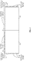
- the resistive touch element 100 includes an ITO track matrix 102 including electrically separate horizontal tracks and electrically separate vertical tracks. Where a horizontal track and vertical track overlap defines a touchell.
- the vertical tracks are connected to a vertical track printed wiring board 104 via a plurality of vertical interconnects 108.
- the horizontal tracks are connected to a horizontal track printed wiring board 106 via a plurality of horizontal interconnects 110.
- Conductive resistive sheathing is more tolerant of variations that could cause serious errors in the pure digital resistive regime.
- the vertical tracks may be spaced 3.175 mm (0.125 inches) or less apart; likewise, the horizontal tracks may be spaced 3.175 mm (0.125 inches) or less apart.
- Narrow spacing may allow contacts identified via digital scan to closely resolve the location of a touch without the need for an analog scan. Removing analog scan eliminates the need for complicated algorithms for determining where the touch occurred.
- the interconnects 108, 110 may comprise tapes or flexes that provide interconnect to the high density ITO track matrix 102 though anisotropic conductive film bonding techniques.
- FIG. 2 a block diagram of a touch screen according to an exemplary embodiment is shown.
- An ITO track matrix 200 is disposed on a substrate 208 with vertical tracks 202 and horizontal tracks 204 defining touchells.
- the vertical tracks 202 and horizontal tracks 204 are connected to one or more integrated circuits disposed on the substrate 208.
- the integrated circuits are connected to a processor via a serial interface 206.
- FIG. 3 a block diagram of an integrated circuit 300 according to an exemplary embodiment, suitable for use in a resistive touch screen is shown.
- the integrated circuit 300 includes a switch network 302 connected to a plurality of vertical tracks or horizontal tracks via a corresponding track interface 312.
- the switch network 312 may operate in a track energize, track discharge, or track detect mode.
- the switch network 302 is in data communication with a programmable comparator network 306 that sends and receives signals to and from the switch network 302.
- the programmable comparator network 306 identifies one or more tracks where a touch has produced a contact with reference to a programmable voltage reference 308 connected to the programmable comparator network 306 and switch network 302.
- the programmable comparator network 306 identifies a plurality of electrical contacts in the switch network 302. At least a subset of the plurality of electrical contacts may be identified as a cluster involving a single touch event but multiple, closely spaced electrical contracts.
- a serial controller 304 connected to the switch network 302 and programmable comparator network 306 sends signals to the programmable comparator network 306 and switch network 302 according to a plurality of position strapping inputs 310 and serial bus inputs.
- passthrough features such as a voltage passthrough, return passthrough, and one or more serial bus features may allow interconnect between multiple independent devices.
- serial bus features may be used to control each integrated circuit 300, transfer data representing touch detection, apply threshold programming, enact device mode select, etc.
- Each integrated circuit 300 may be hardware strap-able to allow all integrated circuits 300 to share the same serial bus.
- Each integrated circuit 300 may utilize the passthrough features to simplify routing and minimize silver epoxy traces. Integrated circuit attachment could be accomplished via processes similar to existing source driver / board bonding techniques or chip on glass techniques.
- the touch screen may be driven from only two sides instead of four.
- the touch screen may be driven from three sides for redundant applications.
- FIG. 4 a block diagram of a dual touch screen according to an exemplary embodiment is shown.
- Two or more ITO track matrices 400, 402 are disposed on one or more substrates with corresponding vertical tracks 404, 408 and horizontal tracks 406, 410 defining touchells specific to one of the ITO track matrices 400, 402.
- the vertical tracks 404, 408 and horizontal tracks 406, 410 are connected to one or more integrated circuits disposed on the substrate.
- the integrated circuits are connected to processors via corresponding serial interfaces 412, 414.
- each ITO track matrix 400, 402 can always resolve two touches, but in some circumstances may not be able to resolve more than two touches. Three touches can be detected in a non-redundant configuration, but a fourth touch could cause ghosting issues, so the third touch may be used as a fault condition and blocked to prevent fourth touch anomalies. Certain scanning techniques may increase detectable touch quantity.
- the two or more ITO track matrices 400, 402 are disposed to serve different sections of a singular display; for example, the two or more ITO track matrices 400, 402 may be disposed side-by-side or covering quadrants of the singular display. Each of the two or more ITO track matrices 400, 402 can separately resolve at least two touches independently.
- integrated circuits may be placed around the entire perimeter of the touchscreen and the touchscreen electrically broken up into quadrants, allowing each quadrant to operate independently, decreasing scan time further but at the cost of more interconnect.
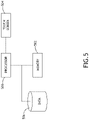
- FIG. 5 a block diagram of system including a resistive touch screen according to an exemplary embodiment is shown.
- the system includes a processor 500 and memory 504 for embodying processor executable code.
- the processor 500 receives signals from a touch screen 504 according to the present disclosure.
- the touch screen 504 includes one or more integrated circuits that resolve one or more touch events on the touch screen 504 and deliver the identified locations to the processor 500.
- the processor 500 is in data communication with a data storage device 506 for storing resolved touch events.
- Embodiments of the present disclosure allow for a much higher intrinsic hardware resolution while using a simple and fast digital scan to detect touches.
- Embodiments of the present disclosure may minimize the frame around the display reducing weight. Furthermore, silver epoxy traces are applied by a silkscreen process and vary in thickness and length producing different cross-sectional areas which hinder analog scan processes.
Landscapes
- Engineering & Computer Science (AREA)
- Theoretical Computer Science (AREA)
- General Engineering & Computer Science (AREA)
- Physics & Mathematics (AREA)
- General Physics & Mathematics (AREA)
- Human Computer Interaction (AREA)
- Computer Hardware Design (AREA)
- Computer Networks & Wireless Communication (AREA)
- Position Input By Displaying (AREA)
Abstract
A touchscreen device utilizes digital scan to resolve a touch location with high precision. The touchscreen device includes touchells of about 3.175 mm by 3.175 mm (0.125 inches by 0.125 inches). An integrated circuit detects contacts in the touchells that resolve to touches on the touchscreen, and communicates those touches to a micro-controller via a serial bus. Silver epoxy interconnects for the tracks are reduced or eliminated. Multiple touchscreens having distinct touchell networks may be disposed to create a larger touchscreen area. Similarly, a single touchscreen may be divided quadrants, each with a distinct touchell network.
Description
- Existing digital resistive touchscreen designs utilize a number of horizontal and vertical oriented Indium-Tin-Oxide (ITO) resistive tracks. Where the ITO tracks intersect is called a "touchell". These touchells are typically large, approximately 12.7 mm by 12.7 mm (0.5 inches x 0.5 inches). This large size is required to limit the number of traces providing interconnect around the perimeter of the touch screen area. Touch detection is achieved through digital scan, which is quick but lacks granularity, and / or analog scan, which offers good measurement granularity and positional data but requires slower analog to digital conversion and data processing. Digital scan and analog scan have been used together to quickly detect a touch using digital scan then performing a more intensive and accurate analog scan in the detected area to precisely locate the touch.
- These methods allow a relatively low resolution digital resistive touch screen to provide high resolution positional data, but the scans, data acquisition, and processing take significant time to accomplish. Furthermore, the silver epoxy traces used around the perimeter to provide interconnect add resistance to the analog measurement which degrades accuracy and must be factored out using the touch controller software. Verifying such complex software can be expensive.
- In one aspect, embodiments of the inventive concepts disclosed herein are directed to a touchscreen device utilizing digital scan to resolve a touch location with high precision. The touchscreen device includes touchells of about 3.175 mm by 3.175 mm (0.125 inches by 0.125 inches). An integrated circuit detects contacts in the touchells that resolve to touches on the touchscreen, and communicates those touches to a microcontroller via a serial bus. In a further aspect, silver epoxy interconnects for the tracks are reduced or eliminated.
- In a further aspect, multiple touchscreens having distinct touchell networks are disposed to create a larger touchscreen area. Similarly, a single touchscreen may be divided quadrants, each with a distinct touchell network.
- It is to be understood that both the foregoing general description and the following detailed description are exemplary and explanatory only and should not restrict the scope of the claims. The accompanying drawings, which are incorporated in and constitute a part of the specification, illustrate exemplary embodiments of the inventive concepts disclosed herein and together with the general description, serve to explain the principles.
- The numerous advantages of the embodiments of the inventive concepts disclosed herein may be better understood by those skilled in the art by reference to the accompanying figures in which:
- FIG. 1
- shows a block diagram of a resistive touch element for a touch screen according to an exemplary embodiment;
- FIG. 2
- shows a block diagram of a touch screen according to an exemplary embodiment;
- FIG. 3
- shows a block diagram of an integrated circuit according to an exemplary embodiment, suitable for use in a resistive touch screen;
- FIG. 4
- shows a block diagram of a dual touch screen according to an exemplary embodiment;
- FIG. 5
- shows a block diagram of system including a resistive touch screen according to an exemplary embodiment;
- Before explaining at least one embodiment of the inventive concepts disclosed herein in detail, it is to be understood that the inventive concepts are not limited in their application to the details of construction and the arrangement of the components or steps or methodologies set forth in the following description or illustrated in the drawings. In the following detailed description of embodiments of the instant inventive concepts, numerous specific details are set forth in order to provide a more thorough understanding of the inventive concepts. However, it will be apparent to one of ordinary skill in the art having the benefit of the instant disclosure that the inventive concepts disclosed herein may be practiced without these specific details. In other instances, well-known features may not be described in detail to avoid unnecessarily complicating the instant disclosure. The inventive concepts disclosed herein are capable of other embodiments or of being practiced or carried out in various ways. Also, it is to be understood that the phraseology and terminology employed herein is for the purpose of description and should not be regarded as limiting.
- As used herein a letter following a reference numeral is intended to reference an embodiment of the feature or element that may be similar, but not necessarily identical, to a previously described element or feature bearing the same reference numeral (e.g., 1, 1a, 1b). Such shorthand notations are used for purposes of convenience only, and should not be construed to limit the inventive concepts disclosed herein in any way unless expressly stated to the contrary.
- Further, unless expressly stated to the contrary, "or" refers to an inclusive or and not to an exclusive or. For example, a condition A or B is satisfied by anyone of the following: A is true (or present) and B is false (or not present), A is false (or not present) and B is true (or present), and both A and B are true (or present).
- In addition, use of the "a" or "an" are employed to describe elements and components of embodiments of the instant inventive concepts. This is done merely for convenience and to give a general sense of the inventive concepts, and "a" and "an" are intended to include one or at least one and the singular also includes the plural unless it is obvious that it is meant otherwise.
- Finally, as used herein any reference to "one embodiment," or "some embodiments" means that a particular element, feature, structure, or characteristic described in connection with the embodiment is included in at least one embodiment of the inventive concepts disclosed herein. The appearances of the phrase "in some embodiments" in various places in the specification are not necessarily all referring to the same embodiment, and embodiments of the inventive concepts disclosed may include one or more of the features expressly described or inherently present herein, or any combination of sub-combination of two or more such features, along with any other features which may not necessarily be expressly described or inherently present in the instant disclosure.
- Broadly, embodiments of the inventive concepts disclosed herein are directed to a touchscreen device utilizing digital scan to resolve a touch location with high precision. The touchscreen device includes touchells of about 3.175 mm by 3.175 mm (0.125 inches by 0.125 inches). An integrated circuit detects contacts in the touchells that resolve to touches on the touchscreen, and communicates those touches to a microcontroller via a serial bus. In a further aspect, silver epoxy interconnects for the tracks are reduced or eliminated. In a further aspect, multiple touchscreens having distinct touchell networks are disposed to create a larger touchscreen area. Similarly, a single touchscreen may be divided quadrants, each with a distinct touchell network.
- Referring to
FIG. 1 , a block diagram of aresistive touch element 100 for a touch screen according to an exemplary embodiment is shown. Theresistive touch element 100 includes an ITOtrack matrix 102 including electrically separate horizontal tracks and electrically separate vertical tracks. Where a horizontal track and vertical track overlap defines a touchell. The vertical tracks are connected to a vertical track printedwiring board 104 via a plurality ofvertical interconnects 108. Likewise, the horizontal tracks are connected to a horizontal track printedwiring board 106 via a plurality ofhorizontal interconnects 110. Conductive resistive sheathing is more tolerant of variations that could cause serious errors in the pure digital resistive regime. - In at least one embodiment, the vertical tracks may be spaced 3.175 mm (0.125 inches) or less apart; likewise, the horizontal tracks may be spaced 3.175 mm (0.125 inches) or less apart. Narrow spacing may allow contacts identified via digital scan to closely resolve the location of a touch without the need for an analog scan. Removing analog scan eliminates the need for complicated algorithms for determining where the touch occurred.
- Reducing the touchell size reduces parasitic capacitance of the sensed tracks, allowing for shortened settling times, faster scans, and reducing overall touch detection latency. Existing resistive touch screens include silver epoxy conductors which are a source of excess resistance that must be accounted for during analog scan; placing tracks closer together would cause electrical interference in the silver epoxy conductors during analog scan. Because embodiments of the present disclosure do not employ analog scan, such interference is obviated.
- Each of the vertical track printed
wiring board 104 and horizontal track printedwiring board 106 and connected to a processor via a serial interface. Theinterconnects ITO track matrix 102 though anisotropic conductive film bonding techniques. - Referring to
FIG. 2 , a block diagram of a touch screen according to an exemplary embodiment is shown. AnITO track matrix 200 is disposed on asubstrate 208 with vertical tracks 202 andhorizontal tracks 204 defining touchells. The vertical tracks 202 andhorizontal tracks 204 are connected to one or more integrated circuits disposed on thesubstrate 208. The integrated circuits are connected to a processor via aserial interface 206. - Referring to
FIG. 3 , a block diagram of anintegrated circuit 300 according to an exemplary embodiment, suitable for use in a resistive touch screen is shown. Theintegrated circuit 300 includes aswitch network 302 connected to a plurality of vertical tracks or horizontal tracks via acorresponding track interface 312. Theswitch network 312 may operate in a track energize, track discharge, or track detect mode. - The
switch network 302 is in data communication with aprogrammable comparator network 306 that sends and receives signals to and from theswitch network 302. Theprogrammable comparator network 306 identifies one or more tracks where a touch has produced a contact with reference to aprogrammable voltage reference 308 connected to theprogrammable comparator network 306 andswitch network 302. In at least one embodiment, theprogrammable comparator network 306 identifies a plurality of electrical contacts in theswitch network 302. At least a subset of the plurality of electrical contacts may be identified as a cluster involving a single touch event but multiple, closely spaced electrical contracts. - In at least one embodiment, a
serial controller 304 connected to theswitch network 302 andprogrammable comparator network 306 sends signals to theprogrammable comparator network 306 andswitch network 302 according to a plurality ofposition strapping inputs 310 and serial bus inputs. In at least one embodiment, passthrough features such as a voltage passthrough, return passthrough, and one or more serial bus features may allow interconnect between multiple independent devices. - Multiple
integrated circuits 300 may be used to scale to larger touch screens. The serial bus features may be used to control eachintegrated circuit 300, transfer data representing touch detection, apply threshold programming, enact device mode select, etc. Eachintegrated circuit 300 may be hardware strap-able to allow allintegrated circuits 300 to share the same serial bus. Eachintegrated circuit 300 may utilize the passthrough features to simplify routing and minimize silver epoxy traces. Integrated circuit attachment could be accomplished via processes similar to existing source driver / board bonding techniques or chip on glass techniques. - In at least one embodiment, the touch screen may be driven from only two sides instead of four. Alternatively, the touch screen may be driven from three sides for redundant applications.
- Referring to
FIG. 4 , a block diagram of a dual touch screen according to an exemplary embodiment is shown. Two or moreITO track matrices vertical tracks horizontal tracks ITO track matrices vertical tracks horizontal tracks serial interfaces - In at least one embodiment, each
ITO track matrix ITO track matrices ITO track matrices ITO track matrices - In at least one embodiment, because interconnects are not necessary on opposing sides of a singular integrated circuit, integrated circuits may be placed around the entire perimeter of the touchscreen and the touchscreen electrically broken up into quadrants, allowing each quadrant to operate independently, decreasing scan time further but at the cost of more interconnect.
- Referring to
FIG. 5 , a block diagram of system including a resistive touch screen according to an exemplary embodiment is shown. The system includes aprocessor 500 andmemory 504 for embodying processor executable code. Theprocessor 500 receives signals from atouch screen 504 according to the present disclosure. Thetouch screen 504 includes one or more integrated circuits that resolve one or more touch events on thetouch screen 504 and deliver the identified locations to theprocessor 500. In at least one embodiment, theprocessor 500 is in data communication with adata storage device 506 for storing resolved touch events. - Embodiments of the present disclosure allow for a much higher intrinsic hardware resolution while using a simple and fast digital scan to detect touches.
- Embodiments of the present disclosure may minimize the frame around the display reducing weight. Furthermore, silver epoxy traces are applied by a silkscreen process and vary in thickness and length producing different cross-sectional areas which hinder analog scan processes.
- It is believed that the inventive concepts disclosed herein and many of their attendant advantages will be understood by the foregoing description of embodiments of the inventive concepts disclosed, and it will be apparent that various changes may be made in the form, construction, and arrangement of the components thereof without departing from the broad scope of the inventive concepts disclosed herein or without sacrificing all of their material advantages; and individual features from various embodiments may be combined to arrive at other embodiments. The form herein before described being merely an explanatory embodiment thereof, it is the intention of the following claims to encompass and include such changes. Furthermore, any of the features disclosed in relation to any of the individual embodiments may be incorporated into any other embodiment.
Claims (15)
- A resistive touch screen apparatus comprising:an ITO track matrix (102) comprising a plurality of vertical tracks (202) and a plurality of horizontal tracks (204);at least one integrated circuit (106) disposed on a first vertical edge of the resistive touch screen apparatus, the at least one integrated circuit in data communication with the plurality of horizontal tracks; andat least one integrated circuit (104) disposed on a first horizontal edge of the resistive touch screen apparatus, the at least one integrated circuit in data communication with the plurality of vertical tracks,wherein:
the at least one integrated circuit disposed on a first vertical edge and the at least one integrated circuit disposed on a first horizontal edge are configured to resolve one or more electrical contacts between horizonal tracks and vertical tracks solely through a digital scan process. - The resistive touch screen apparatus of Claim 1, wherein:the plurality of horizontal tracks are spaced no more than four millimeters apart; andthe plurality of vertical tracks are spaced no more than four millimeters apart.
- The resistive touch screen apparatus of Claim 1 or 2, wherein:the ITO track matrix comprises at least two independent ITO track matrices (400, 402) disposed over different portions of a common display; andthe at least one integrated circuit disposed on the first horizontal edge comprises a first integrated circuit disposed on the first horizontal edge associated with a first ITO track matrix, and a second integrated circuit disposed on the first horizontal edge associated with a second ITO track matrix; andfurther comprising at least one integrated circuit disposed on a second vertical edge of the resistive touch screen apparatus associated with the second ITO track matrix.
- The resistive touch screen apparatus of Claim 3, wherein:the ITO track matrix comprises at least four independent ITO track matrices disposed over different quadrants of the common display;the at least one integrated circuit disposed on the first vertical edge comprises a first integrated circuit disposed on the first vertical edge associated with the first ITO track matrix, and a second integrated circuit disposed on the first vertical edge associated with a third ITO track matrix; andand the at least one integrated circuit disposed on the second vertical edge comprises a first integrated circuit disposed on the second vertical edge associated with the second ITO track matrix, and a second integrated circuit disposed on the second vertical edge associated with a fourth ITO track matrix; andfurther comprising at least two integrated circuits disposed on a second horizontal edge of the resistive touch screen apparatus associated with the third ITO track matrix and the fourth ITO track matrix.
- The resistive touch screen apparatus of any preceding Claim, further comprising a plurality of silver epoxy traces disposed along the first vertical edge and first horizontal edge, each of the silver epoxy traces associated with two horizontal tracks or two vertical tracks.
- The resistive touch screen apparatus of any preceding Claim, further comprising one or more serial buses connecting each of the integrated circuits to a controller (304).
- A mobile platform comprising:
a resistive touch screen apparatus as claimed in any preceding claim. - A computer system comprising:a resistive touch screen (504) comprising:an ITO track matrix (102) comprising a plurality of vertical tracks (202) and a plurality of horizontal tracks (204);at least one integrated circuit (106) disposed on a first vertical edge of the resistive touch screen apparatus, the at least one integrated circuit in data communication with the plurality of horizontal tracks; andat least one integrated circuit (104) disposed on a first horizontal edge of the resistive touch screen apparatus, the at least one integrated circuit in data communication with the plurality of vertical tracks; andat least one processor (500) in data communication with the integrated circuits and a memory (502) storing processor executable code for configuring the at least one processor to:receive one or more digital electrical signals generated via one or more electrical contacts between vertical tracks and horizontal tracks; andresolve the digital electrical signals into one or more touch events on the resistive touch screen,wherein:
the at least one integrated circuit disposed on a first vertical edge and the at least one integrated circuit disposed on a first horizontal edge are configured to resolve one or more electrical contacts between horizonal tracks and vertical tracks solely through a digital scan process. - The computer system of Claim 8, wherein:the plurality of horizontal tracks are spaced no more than four millimeters apart; andthe plurality of vertical tracks are spaced no more than four millimeters apart.
- The computer system of Claim 8 or 9, wherein:the ITO track matrix comprises at least two independent ITO track matrixes disposed over different portions of a common display; andthe at least one integrated circuit disposed on the first horizontal edge comprises a first integrated circuit disposed on the first horizontal edge associated with a first ITO track matrix, and a second integrated circuit disposed on the first horizontal edge associated with a second ITO track matrix; andfurther comprising at least one integrated circuit disposed on a second vertical edge of the resistive touch screen apparatus associated with the second ITO track matrix.
- The computer system of Claim 10, wherein:the ITO track matrix comprises at least four independent ITO track matrixes disposed over different quadrants of the common display;the at least one integrated circuit disposed on the first vertical edge comprises a first integrated circuit disposed on the first vertical edge associated with the first ITO track matrix, and a second integrated circuit disposed on the first vertical edge associated with a third ITO track matrix; andand the at least one integrated circuit disposed on the second vertical edge comprises a first integrated circuit disposed on the second vertical edge associated with the second ITO track matrix, and a second integrated circuit disposed on the second vertical edge associated with a fourth ITO track matrix; andfurther comprising at least two integrated circuits disposed on a second horizontal edge of the resistive touch screen apparatus associated with the third ITO track matrix and the fourth ITO track matrix.
- The computer system of any of Claims 8 to 11, further comprising a plurality of silver epoxy traces disposed along the first vertical edge and first horizontal edge, each of the silver epoxy traces associated with two horizontal tracks or two vertical tracks.
- The computer system of any of Claims 8 to 12, further comprising one or more serial buses connecting each of the integrated circuits to the processor.
- The computer system of any of Claims 8 to 13, wherein the at least one processor is further configured to:associate a plurality of digital signals with a touch event based on temporal proximity, physical proximity, and continuity; andresolve the first touch event to a location of the resistive touch screen via averaging the locations of the digital signals.
- The computer system of any of Claims 8 to 14, wherein:the one or more digital signals comprise a plurality of digital signals generated via at least two touch events; andthe at least one processor is further configured to:associate a first set of digital signals with a first touch event based on temporal proximity, physical proximity, and continuity; andresolve the first touch event based on the first set of digital signals.
Applications Claiming Priority (1)
| Application Number | Priority Date | Filing Date | Title |
|---|---|---|---|
| US17/143,016 US11429224B2 (en) | 2021-01-06 | 2021-01-06 | Eliminating interconnect induced inaccuracies and reducing scan time using a high granularity resistive touch screen |
Publications (1)
| Publication Number | Publication Date |
|---|---|
| EP4027225A1 true EP4027225A1 (en) | 2022-07-13 |
Family
ID=79024942
Family Applications (1)
| Application Number | Title | Priority Date | Filing Date |
|---|---|---|---|
| EP21218225.7A Withdrawn EP4027225A1 (en) | 2021-01-06 | 2021-12-29 | Eliminating interconnect induced inaccuracies and reducing scan time using a high granularity resistive touch screen |
Country Status (2)
| Country | Link |
|---|---|
| US (1) | US11429224B2 (en) |
| EP (1) | EP4027225A1 (en) |
Citations (4)
| Publication number | Priority date | Publication date | Assignee | Title |
|---|---|---|---|---|
| US20060097991A1 (en) * | 2004-05-06 | 2006-05-11 | Apple Computer, Inc. | Multipoint touchscreen |
| US20110122088A1 (en) * | 2009-11-23 | 2011-05-26 | Elan Microelectronics Corporation | Passive architecture and control method for scanning a touch panel |
| US20120212425A1 (en) * | 2011-02-23 | 2012-08-23 | Honeywell International Inc. | Resistive touch screen displays and systems |
| US20190087042A1 (en) * | 2017-09-15 | 2019-03-21 | Sigmasense, Llc. | Touchscreen display with concurrent touch and display operations |
Family Cites Families (33)
| Publication number | Priority date | Publication date | Assignee | Title |
|---|---|---|---|---|
| US5159159A (en) * | 1990-12-07 | 1992-10-27 | Asher David J | Touch sensor and controller |
| US5392058A (en) * | 1991-05-15 | 1995-02-21 | Sharp Kabushiki Kaisha | Display-integrated type tablet device |
| US5534892A (en) * | 1992-05-20 | 1996-07-09 | Sharp Kabushiki Kaisha | Display-integrated type tablet device having and idle time in one display image frame to detect coordinates and having different electrode densities |
| US6819316B2 (en) * | 2001-04-17 | 2004-11-16 | 3M Innovative Properties Company | Flexible capacitive touch sensor |
| US9710095B2 (en) | 2007-01-05 | 2017-07-18 | Apple Inc. | Touch screen stack-ups |
| US8519965B2 (en) * | 2008-04-23 | 2013-08-27 | Motorola Mobility Llc | Multi-touch detection panel with disambiguation of touch coordinates |
| WO2010016736A2 (en) | 2008-08-08 | 2010-02-11 | Ahn Seung Duk | Analog-digital hybrid touch panel apparatus and a recognition method thereof |
| TWI408578B (en) * | 2009-01-22 | 2013-09-11 | Wintek Corp | Resistive touch control device and driving method and driving controller thereof |
| US8599565B2 (en) * | 2009-04-21 | 2013-12-03 | Fujitsu Component Limited | Touchscreen panel, electronic apparatus and method of fabricating touchscreen panel |
| TWI450176B (en) * | 2009-06-18 | 2014-08-21 | Wintek Corp | Touch sensing method for resistive type touch apparatus |
| US8330741B1 (en) * | 2009-08-28 | 2012-12-11 | Altera Corporation | Multi-touch decoder for digital resistive screen overlay |
| KR101059098B1 (en) | 2009-12-24 | 2011-08-24 | 이성호 | Touch cell structure of touch panel, touch panel and touch input detection method using same |
| KR101680256B1 (en) * | 2010-11-08 | 2016-12-13 | 삼성디스플레이 주식회사 | Touch Screen Panel in Resistive Type |
| TWI515614B (en) | 2010-12-24 | 2016-01-01 | 杜彥宏 | Multi-stage scanning touch position detecting device and method |
| US9081450B1 (en) * | 2011-06-09 | 2015-07-14 | Maxim Integrated Products, Inc. | Identifying hover and/or palm input and rejecting spurious input for a touch panel |
| US20130015906A1 (en) * | 2011-07-13 | 2013-01-17 | Silicon Integrated Systems Corp. | Touch Panel Device |
| US8963561B2 (en) | 2011-11-03 | 2015-02-24 | Atmel Corporation | Randomizing one or more micro-features of a touch sensor |
| US9965106B2 (en) * | 2011-11-22 | 2018-05-08 | Atmel Corporation | Touch screen with electrodes positioned between pixels |
| US9134827B2 (en) * | 2011-12-28 | 2015-09-15 | Synaptics Incorporated | System and method for mathematically independent signaling in gradient sensor devices |
| US9817523B2 (en) * | 2012-02-09 | 2017-11-14 | Qualcomm Incorporated | Capacitive touch panel for mitigating and/or exaggerating floating condition effects |
| GB2510600B (en) * | 2013-02-08 | 2015-05-20 | R & D Core Ltd | Calibration of Contact Sensor |
| US9612677B2 (en) * | 2013-06-28 | 2017-04-04 | Atmel Corporation | Pseudo driven shield |
| CN104881161B (en) * | 2014-02-27 | 2017-12-01 | 财团法人工业技术研究院 | Touch panel |
| US10168732B2 (en) * | 2014-02-27 | 2019-01-01 | Industrial Technology Research Institute | Touch panel and sensing method thereof |
| KR101756693B1 (en) | 2014-08-11 | 2017-07-11 | 주식회사 임프레시보코리아 | Method and device for recognizing user operation, and non-temporary computer-readable recording medium |
| TWI531942B (en) | 2014-08-19 | 2016-05-01 | 原相科技股份有限公司 | Touch display device and operating method thereof |
| US20160188098A1 (en) * | 2014-12-26 | 2016-06-30 | Lg Innotek Co., Ltd. | Touch window and touch device |
| TWI576739B (en) * | 2015-11-05 | 2017-04-01 | 宏碁股份有限公司 | Touch display device and manufacturing method thereof |
| US9846509B2 (en) * | 2015-11-17 | 2017-12-19 | Rockwell Collins, Inc. | Fail operational redundant digital resistive touchscreen |
| US10275078B1 (en) * | 2017-03-20 | 2019-04-30 | Rockwell Collins, Inc. | Split resistive touch sensor |
| US10474304B1 (en) | 2018-05-14 | 2019-11-12 | Sharp Kabushiki Kaisha | Programmable active matrix of electrodes |
| KR102129527B1 (en) * | 2018-12-14 | 2020-07-02 | 한국과학기술연구원 | Highly dielectric elastic structure and method for preparing the same |
| US11237687B2 (en) * | 2019-01-25 | 2022-02-01 | Samsung Electronics Co., Ltd. | Systems and methods for touch detection using electric field tomography through resistive sheet |
-
2021
- 2021-01-06 US US17/143,016 patent/US11429224B2/en active Active
- 2021-12-29 EP EP21218225.7A patent/EP4027225A1/en not_active Withdrawn
Patent Citations (4)
| Publication number | Priority date | Publication date | Assignee | Title |
|---|---|---|---|---|
| US20060097991A1 (en) * | 2004-05-06 | 2006-05-11 | Apple Computer, Inc. | Multipoint touchscreen |
| US20110122088A1 (en) * | 2009-11-23 | 2011-05-26 | Elan Microelectronics Corporation | Passive architecture and control method for scanning a touch panel |
| US20120212425A1 (en) * | 2011-02-23 | 2012-08-23 | Honeywell International Inc. | Resistive touch screen displays and systems |
| US20190087042A1 (en) * | 2017-09-15 | 2019-03-21 | Sigmasense, Llc. | Touchscreen display with concurrent touch and display operations |
Also Published As
| Publication number | Publication date |
|---|---|
| US11429224B2 (en) | 2022-08-30 |
| US20220214793A1 (en) | 2022-07-07 |
Similar Documents
| Publication | Publication Date | Title |
|---|---|---|
| US11829543B2 (en) | Method for detecting and confirming a touch input | |
| US8274488B2 (en) | Touch location detecting panel having a simple layer structure | |
| EP3153946B1 (en) | Embedded touchscreen and display device | |
| EP3151100B1 (en) | Embedded touchscreen and display device | |
| US8988387B2 (en) | Touch sensor panel with in-plane backup bypass connections | |
| EP3252575B1 (en) | Touch panel, display apparatus, and touch driving method | |
| US20090002338A1 (en) | Screen input type image display | |
| US20110063247A1 (en) | Touch sensing apparatus with parasitic capacitance prevention structure | |
| US20160364060A1 (en) | Touch panel, touch positioning method thereof and display device | |
| US20130100041A1 (en) | System for a single-layer sensor having reduced number of interconnect pads for the interconnect periphery of the sensor panel | |
| US20140368750A1 (en) | Single-layer mutual capacitive touch screen | |
| US20110242015A1 (en) | Touch input device | |
| CN112925448A (en) | Touch display panel, detection method thereof and touch display device | |
| US10275077B2 (en) | Touch control display panel, touch control display device and driving method | |
| CN104571770B (en) | In-cell touch panel, touch control detecting method and display device | |
| CN101339481A (en) | Electric resistance array touch screen | |
| JP2018063666A (en) | Display driver, display device, and display panel | |
| WO2016195308A1 (en) | Method for correcting sensitivity of touch input device that detects touch pressure and computer-readable recording medium | |
| CN112083836B (en) | A touch panel and its driving method, and a touch display device | |
| JP2024507594A (en) | Electrochromic devices and electronic equipment | |
| US11429224B2 (en) | Eliminating interconnect induced inaccuracies and reducing scan time using a high granularity resistive touch screen | |
| US9977548B2 (en) | Touch panel and touch electrode structure thereof | |
| US20260037097A1 (en) | Touch display panel, touch display apparatus, and electronic device | |
| CN102650915A (en) | Digital touch screen and touch positioning method thereof | |
| US12260054B2 (en) | Touch substrate and display panel |
Legal Events
| Date | Code | Title | Description |
|---|---|---|---|
| PUAI | Public reference made under article 153(3) epc to a published international application that has entered the european phase |
Free format text: ORIGINAL CODE: 0009012 |
|
| STAA | Information on the status of an ep patent application or granted ep patent |
Free format text: STATUS: THE APPLICATION HAS BEEN PUBLISHED |
|
| AK | Designated contracting states |
Kind code of ref document: A1 Designated state(s): AL AT BE BG CH CY CZ DE DK EE ES FI FR GB GR HR HU IE IS IT LI LT LU LV MC MK MT NL NO PL PT RO RS SE SI SK SM TR |
|
| STAA | Information on the status of an ep patent application or granted ep patent |
Free format text: STATUS: THE APPLICATION IS DEEMED TO BE WITHDRAWN |
|
| 18D | Application deemed to be withdrawn |
Effective date: 20230114 |