EP4024713A1 - System and method for analog-to-digital signal conversion - Google Patents
System and method for analog-to-digital signal conversion Download PDFInfo
- Publication number
- EP4024713A1 EP4024713A1 EP21150013.7A EP21150013A EP4024713A1 EP 4024713 A1 EP4024713 A1 EP 4024713A1 EP 21150013 A EP21150013 A EP 21150013A EP 4024713 A1 EP4024713 A1 EP 4024713A1
- Authority
- EP
- European Patent Office
- Prior art keywords
- digital
- signal
- amplifier
- capacitor bank
- capacitor
- Prior art date
- Legal status (The legal status is an assumption and is not a legal conclusion. Google has not performed a legal analysis and makes no representation as to the accuracy of the status listed.)
- Granted
Links
Images




Classifications
-
- H—ELECTRICITY
- H03—ELECTRONIC CIRCUITRY
- H03M—CODING; DECODING; CODE CONVERSION IN GENERAL
- H03M1/00—Analogue/digital conversion; Digital/analogue conversion
- H03M1/12—Analogue/digital converters
- H03M1/124—Sampling or signal conditioning arrangements specially adapted for A/D converters
- H03M1/1245—Details of sampling arrangements or methods
- H03M1/125—Asynchronous, i.e. free-running operation within each conversion cycle
-
- H—ELECTRICITY
- H03—ELECTRONIC CIRCUITRY
- H03M—CODING; DECODING; CODE CONVERSION IN GENERAL
- H03M1/00—Analogue/digital conversion; Digital/analogue conversion
- H03M1/10—Calibration or testing
- H03M1/1009—Calibration
- H03M1/1014—Calibration at one point of the transfer characteristic, i.e. by adjusting a single reference value, e.g. bias or gain error
-
- H—ELECTRICITY
- H03—ELECTRONIC CIRCUITRY
- H03M—CODING; DECODING; CODE CONVERSION IN GENERAL
- H03M1/00—Analogue/digital conversion; Digital/analogue conversion
- H03M1/12—Analogue/digital converters
- H03M1/48—Servo-type converters
-
- H—ELECTRICITY
- H03—ELECTRONIC CIRCUITRY
- H03M—CODING; DECODING; CODE CONVERSION IN GENERAL
- H03M1/00—Analogue/digital conversion; Digital/analogue conversion
- H03M1/12—Analogue/digital converters
- H03M1/50—Analogue/digital converters with intermediate conversion to time interval
-
- H—ELECTRICITY
- H03—ELECTRONIC CIRCUITRY
- H03M—CODING; DECODING; CODE CONVERSION IN GENERAL
- H03M1/00—Analogue/digital conversion; Digital/analogue conversion
- H03M1/06—Continuously compensating for, or preventing, undesired influence of physical parameters
- H03M1/0614—Continuously compensating for, or preventing, undesired influence of physical parameters of harmonic distortion
Definitions
- the invention relates to analog-to-digital signal conversion, especially to asynchronous analog-to-spike converter architectures in wireless sensor nodes.
- minimizing power consumption in wireless sensor nodes is important to ensure a long lifetime of the battery.
- One way to minimize the power consumption is by making the power consumption activity dependent. For many biological signals, such as ECG, EEG, neuron signals, only small pieces in time are important to process. This reduced data helps, for example, the transmitter, since it now needs to transmit less data and thus uses less power. Since the transmitter power consumption is usually much higher than other components such as the front-end, reducing the power of the transmitter has a significant impact on the total power consumption.
- the analog information is continuously monitored by a front-end, then converted by an analog-to-digital converter (ADC), and then sent out via a transmitter.
- ADC analog-to-digital converter
- an ADC samples the signal at every clock pulse, which is independent of the input signal. This means that even when the signal does not change, samples are still being generated.
- a different way of sampling is called level-crossing sampling, where a sampling instance occurs, i.e. the generation of a sample, only when the amplitude of the signal changed by a fixed step.
- the patent document US 9,252,658 B2 shows such level-crossing based sampling, for instance.
- an object of the invention is to provide a system and a method for analog-to-digital signal conversion, which can address the above-mentioned limitations.
- a system for analog-to-digital signal conversion comprises an analog input signal, a digital-to-analog converter configured to generate a reference signal, and an amplifier configured to amplify an error signal comprising a difference between the analog input signal and the reference signal.
- the system further comprises a level-crossing based sampling circuit comprising a first comparator configured to compare the error signal with respect to a first reference level, and a second comparator configured to compare the error signal with respect to a second reference level, thereby generating event-based reset signals corresponding to a plurality of sampling instances in order to reset the digital-to-analog converter and further to shift the first reference level and the second reference level through the digital-to-analog converter.
- the system comprises a trigger circuit configured to generate reset signals asynchronous to the event-based reset signals in order to reset the digital-to-analog converter.
- the invention proposes additional resets for resetting the DAC in addition to the event-based resets correspond to each sampling instances, i.e. to each instance of sample generation.
- Said event-based reset signals or spikes reset the DAC and further change the reference signal level (e.g. voltage level) through the DAC, especially by shifting the first reference level and the second reference level via the DAC.
- the resets are not clock-generated so as to eliminate the necessity of having on-board oscillators.
- the amplifier, or a so-called pre-amplifier, shared by the comparators solves the problem with the required area for the calibration of the comparators. Any error made after the pre-amplifier is divided by the gain of said pre-amplifier, thereby relaxing the offset requirement of the comparators.
- the level-crossing based sampling circuit further comprises a digital logic circuit configured to generate an amplitude and a time stamp corresponding to each of the plurality of sampling instances.
- the digital logic circuit is further configured to feedback the amplitude corresponding to each of the plurality of sampling instances to the digital-to-analog converter in order to generate the reference signal.
- the digital logic circuit may comprise an up/down counter that functions as a digital integrator and a timer that records the time in-between two sampling instances or samples. For each sampling instances, the output of the comparators toggles and the digital logic circuit starts to update the up/down counter to refresh the comparison window.
- the digital-to-analog converter is a capacitive charge transfer digital-to-analog converter, more preferably a switched capacitor based digital-to-analog converter.
- the trigger circuit comprises a switched capacitor arrangement in order to replicate the digital-to-analog converter.
- capacitive DAC for reference signal or voltage generation advantageously facilitates smaller area and low power consumption.
- replicating the DAC e.g. replicating the switched-capacitor arrangement of the DAC, the leakage induced error of the DAC can be potentially measured during operation.
- the level-crossing based sampling circuit further comprises a first capacitor bank coupled between a common node downstream to the amplifier and the first comparator, where the first capacitor bank is configured to store the first reference level based on the reference signal.
- the level-crossing based sampling circuit further comprises a second capacitor bank coupled between the common node downstream to the amplifier and the second comparator, where the second capacitor bank is configured to store the second reference level based on the reference signal.
- only one pre-amplifier is used to store the reference levels, i.e. two references that are two LSB apart, in order to compare the input signal against said reference levels. This further reduces the overall area requirement of the ADC in addition to input referred offset compensation for the comparators.
- the first capacitor bank and/or the second capacitor bank comprises a pair of parallel capacitors and switching arrangements.
- the switching arrangements are configured to be operable such that at least one capacitor of the pair of parallel capacitors stores a charge proportional to two least significant bit (LSB) in addition to an offset error of the amplifier.
- the switching arrangements are configured to be operable such that at least one capacitor of the pair of parallel capacitors stores a charge proportional to the offset error of the amplifier.
- the switching arrangements are configured to be operable such that the pair of parallel capacitors each store a charge proportional to one least significant bit (LSB). This effectively provides two references that are two LSB apart for the ADC to compare the input signal against said references.
- the pair of parallel capacitors of the first capacitor bank and/or the second capacitor bank are equal in dimension, preferably identical parallel plate capacitors.
- the digital logic circuit is configured to generate control signals for the switching arrangements of the first capacitor bank and/or the second capacitor bank. This advantageously provides a simple arrangement for storing the references.
- a method for signal conversion in a system for analog-to-digital signal conversion.
- the method comprises the step of providing an analog input signal.
- the method further comprises the step of generating a reference signal by a digital-to-analog converter.
- the method comprises the step of generating an error signal comprising a difference between the analog input signal and the reference signal and amplifying the error signal by an amplifier.
- the method comprises the step of comparing the error signal with respect to a first reference level and a second reference level and generating event-based reset signals corresponding to a plurality of sampling instances by a level-crossing based sampling circuit.
- the method further comprises the step of generating reset signals asynchronous to the event-based reset signals by a trigger circuit.
- the invention proposes additional resets for resetting the DAC in addition to the event-based resets correspond to each sampling instances, i.e. to each instances of sample generation, which effectively minimize the requirements for a longer hold time of the DAC. Moreover, the offset requirements of the comparators are relaxed by the gain of the amplifier, which is shared by both comparators.
- the method further comprises the step of providing a first capacitor bank comprising a pair of parallel capacitors and switching arrangements in order to store the first reference level and providing a second capacitor bank comprising a pair of parallel capacitors and switching arrangements in order to store the second reference level.
- the method further comprises the step of operating the switching arrangements of the first capacitor bank and/or of the second capacitor bank for storing, by at least one capacitor of the pair of capacitors, a charge proportional to two least significant bit (LSB) in addition to an offset error of the amplifier, and for storing, by at least one capacitor of the pair of capacitors, a charge proportional to the offset error of the amplifier, and for storing, by each of the pair of capacitors, a charge proportional to one least significant bit (LSB).
- LSB charge proportional to two least significant bit
- FIG. 1A shows a conventional level-crossing analog-to-digital converter (LC-ADC) that converts the analog signal Vin into discrete samples at a numerous sampling instances.
- LC-ADC uses level-crossing detection to sample the analog signal Vin.
- the LC-ADC consists of two comparators 104,105, a digital-to-analog converter (DAC) 101 and a logic block 106 comprising an up/down counter. Two threshold levels V H and V L are set to identify the analog signal Vin.
- the threshold levels V H and V L are generated via the DAC 101 with a difference equal to the quantization step. Hence, in digital representation, the difference between V H and V L is equal to 2 least significant bit (LSB).
- the error 102 between Vin and V H is fed to the comparator 104 and the error 103 between Vin and V L is fed to the comparator 105 for comparison, for example.
- the sampling instance or sampling occurs when Vin is either higher than V H or lower than V L .
- the logic block 106 sets an increment signal or a decrement signal accordingly to activate the up/down counter, thereby incrementing or decrementing the counter output by 1 LSB.
- This further controls the DAC 101 whose generated signals V H and V L will be updated to keep tracking the analog signal Vin.
- the analog signal Vin is between V H and V L , no changes occur on the up/down counter output or DAC 101 output, therefore no new samples are taken.
- the sampling instances are further shown in Fig. 1B , where the analog signal Vin is sampled at different instances, e.g. 107, based on a sampling window 108 defined by the difference between V H and V L .
- the two comparators 104,105 have a different offset voltage, which degrades the SNDR and therefore is required to be kept small in order to achieve a high SNDR.
- One possible solution is to add a foreground calibration, especially a resistive calibration DAC that can permanently hold the reference voltage.
- this solution comes with the cost of increased power consumption and further increases the overall area due to the requirement of an additional clock.
- said calibration scheme is not able to counter offset drifts, which might hinder the performance in a real application.
- a capacitive DAC for the reference voltage generation is the most common architecture for LC-ADC due to its small area and power consumption.
- the problem with a capacitive DAC however is that it is not possible to hold the charge indefinitely. Since the DAC 101 is only reset when the analog signal Vin crosses V H or V L , the DAC 101 is not reset when the analog signal Vin changes slowly. This results in the leakage induced error becoming large and therefore degrades the SNDR, especially for low frequencies.
- the system 200 (can also be referred to as an analog-to-digital converter) comprises an analog input signal 201 to be converted into discrete samples while a reference signal 203 is generated by a digital-to-analog converter (DAC) 202 for domain conversion.
- the analog input signal 201 and the reference signal 203 are summed at a subtractor 204, which results in an error or difference signal (voltage, charge or current) 205 comprising a difference between the analog input signal 201 and the reference signal 203.
- Said error signal 205 is fed to an amplifier or a pre-amplifier 206 that amplifies the error signal by the gain of the amplifier 206.
- the amplifier 206 advantageously mitigates any signal loss due to the subtraction of the analog input signal 201 and the reference signal 203 at the subtractor 204.
- the amplifier 206 provides a common node 207 at its output, which commonly shares the common node 207 with a first path 210 connecting to a non-inverting input of a first comparator 214 and a second path 211 connecting an inverting input of a second comparator 215.
- a first capacitor bank 208 is located at the first path 210 between the common node 207 and the non-inverting input of the first comparator 214.
- a second capacitor bank 209 is located at the second path 211 between the common node 207 and the inverting input of the second comparator 215.
- An inverting input of the first comparator 214 and a non-inverting input of the second comparator 215 are commonly connected to ground.
- the first capacitor bank 208 and the second capacitor bank 209 each comprise a pair of parallel capacitors (not shown) and switching arrangements, whose functionalities will be discussed in a later section of this description.
- the output 216 of the first comparator 214 and the output 217 of the second comparator 215 are connected to a digital logic circuit 218.
- Said digital logic circuit 218 is composed of but not limited to an up/down counter and a timer (e.g. time-to-digital converter).
- the first capacitor bank 208, the second capacitor bank 209, the first comparator 214, the second comparator 215, and the digital logic circuit 218 collectively form a level-crossing based sampling circuit 220.
- the sampled output 219 from the digital logic circuit 218 is fed back to the DAC 202 over a feedback path 222 in order to generate the reference signal 203.
- the digital logic circuit 218 further outputs event-based reset signals 221 for each sampling instance or samples (i.e. up/down event) in order to reset the DAC 202.
- the system further comprises a triggering arrangement 230 for resetting the DAC 202 in addition to the event-based reset signals 221.
- Said triggering arrangement 230 comprises a trigger circuit 223 that generates reset signals 224 asynchronous to the event-based reset signals 221.
- the triggering arrangement 230 further comprises a two-input OR gate 225 that inputs the event-based reset signals 221 from the digital logic circuit 218 and the trigger signals 224 from the trigger circuit 224, thereby outputting a trigger signal 226 whenever either one or both of the inputs of the OR gate 225 is high.
- the OR gate 225 can be implemented with any logical combinations or gates as long as the output of said combinations is high when either one or both of the inputs are high.
- the error signal 205 is amplified by the amplifier 206 and is further compared with a first reference level stored at the first capacitor bank 208 by the first comparator 214. Ideally, the first reference level gives the upper boundary of the comparison window. Similarly, the error signal 205 is amplified by the amplifier 206 and is further compared with a second reference level stored at the second capacitor bank 209 by the second comparator 215. Ideally, the second reference level gives the lower boundary of the comparison window.
- the storing method of the reference levels at the first capacitor bank 208 and at the second capacitor bank 209 will be discussed later in detail.
- the event-based reset signals 221 from the digital logic circuit 218 further change the reference signal level by shifting the first reference level and the second reference level via the DAC 202, thereby shifting the comparison window for subsequent comparisons.
- the first comparator 214 and the second comparator 215 respectively compare the error signal 205 with respect to a fixed comparison window, i.e. in digital representation of 2 LSB, and toggles its output whenever it detects a level crossing. This result in the generation of respective sampling instances or samples and further toggles the up/down counter to generate an up or down event. Since the first comparator 214 and the second comparator 215 compare the error signal 205 instead of the input analog signal 201, the comparator common-mode range is reduced significantly and optimization of the comparators targeting at a specific reference level can be performed with ease. The related effects that result from comparator offset and distortion are thus reduced. More importantly, similar performance is achievable for the comparators with lower power consumption.
- the amplifier 206 is shared by the first comparator 214 and the second comparator 215.
- any error made after the amplifier 206 is divided by the gain of the amplifier 206, which relaxes the offset requirement of the first comparator 214 and the second comparator 215.
- the output of the first comparator 214 and/or the output of the second comparator 215 toggle and the digital control circuit 218 updates the up/down counter in order to refresh the comparison window, thereby resetting the DAC 202.
- Said up/down counter acts as a digital integrator and the time in between two sampling instances are recorded by the timer.
- the trigger circuit 223 further generates asynchronous trigger signals 224, which are cumulatively operating on the DAC 202 to reset the DAC 202, even when there is no sampling instances recorded at the digital logic circuit 218.
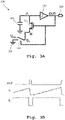
- Fig. 3A shows the trigger circuit 300, which can be implemented as the trigger circuit 223 of Fig. 2 .
- Fig. 3B shows operation stages of said trigger circuit 300.
- the DAC 202 is a capacitive DAC
- the trigger circuit 300 is realized so that it replicates said capacitive DAC. Since the leakage cannot be directly measured in the DAC 202, the replica circuit 300 is able to sense the leakage and further to act accordingly to mitigate the leakage.
- the trigger circuit 300 comprises a capacitor 301 connected to ground at one node and further provides a common port A to the other node.
- a NMOS switch 302 is coupled. Particularly, the drain of the NMOS switch is coupled to the common node A whereas the source of the NMOS switch is coupled to a node B.
- a second switch 304 is coupled to the node B that initially connects the node B to a bias voltage V DD .
- a comparator 303 is coupled to the common node A and the output OUT of the comparator 303 is fed back to the gate of the NMOS switch 302 and further used to toggle the second switch 304 between the bias voltage V DD and ground 305.
- the output OUT is low. Due to leakage through the NMOS switch 302, the voltage of the capacitor 301 rises. When the voltage of the capacitor 301 exceeds the trip point of the comparator 303, the output OUT goes high. This causes the NMOS switch 302 to turn on and the second switch 304 to toggle to ground 305. The capacitor 301 then discharges through the NMOS switch 302 and the voltage on the capacitor goes low again. This further sets the output OUT low and restarts the cycle.
- the operation phases can be seen in Fig. 3B where the OUT is initially low and the voltage at A is rising, i.e. the charging state of the capacitor 301.
- the voltage at B is at V DD .
- the comparator 303 When the voltage at A rises to the trip point of the comparator 303, the comparator 303 output toggles, and thus OUT becomes high.
- the capacitor 301 discharges and the voltage at A goes low as well as the voltage at B, since the latter is now connected to ground. This further sets the output OUT low and restarts the cycle.
- the OUT signals therefore represent the additional trigger signals 224 that are generated asynchronous to the event-based trigger signals 221 from the level-crossing based sampling circuit 220.
- FIG. 4A shows the leakage induced error caused by a finite hold time of the digital-to-analog converter 202.
- a capacitive DAC is the most common architecture for the reference generation but suffers from a finite hold time.
- the signal Vin represents the analog input signal 201 which is sampled along a sampling window provided by the upper boundary or first reference level V H and the lower boundary or second reference level V L .
- the event-based reset signals 221 are shown as spikes respective to each up/down events, i.e. sampling instances.
- the drift in the reference is very short and therefore the leakage induced error is not significant.
- the DAC reference drifts away and introduces a large leakage induced error.
- the DAC 202 resets at point 401 and further drifts at 402 and further resets at 403. Since the time between crossings is short, the leakage induced error is not significant. However, at 404, the DAC drifts for a longer time that introduces a large leakage induced error.
- Fig. 4B shows the proposed technique of having additional resets in order to mitigate the large leakage induced error in the DAC 202.
- Additional trigger signals 224 are generated along with the event-based reset signals 221, especially asynchronous to the event-based reset signals 221.
- the DAC 202 resets and further drifts at 406, however, is not drifting anymore due to the additional resets 224.
- the DAC 202 resets at 407 instead. As a result, a large portion of the leakage induced error is mitigated.
- Fig. 5A shows the trigger circuit 500, which can be implemented as the trigger circuit 223 of Fig. 2 .
- Fig. 5B shows the output of said trigger circuit 500.
- the trigger circuit 223 can be implemented as a current starved ring oscillator circuit 500 as shown in Fig. 5A .
- the ring oscillator 500 comprises a first inverter stage 501, a second inverter stage 502 and a third inverter stage 503, where the output 504 of the third inverter stage 503 is fed back to the first inverter stage 501.
- three inverter stages are illustrated herein, it is to be noted that any odd number of inverter stages can be implemented as long as the total propagation delay, i.e. the frequency of oscillation, meets the target specification.
- each capacitor bank comprises a pair of parallel capacitors 601 and 602, and at least four switches S 1 , S 2 , S 3 and S 4 .
- Said capacitors 601 and 602 are equally sized capacitors.
- the amplifier 206 output is connected to one end of the capacitor 601 and the other end of the capacitor 601 is connected to the switches S 1 and S 4 , where the switch S 1 can be toggled to ground 603.
- the switch S 2 is connected in parallel with the capacitor 602 to the switch S 4 and the switch S 3 is connected in series with the capacitor 602, where the switch S 3 can be toggled to ground 604.
- the first path 210 and/or the second path 211, as shown in Fig. 2 is coupled at the parallel junction between the switch S 4 , the switch S 2 and the capacitor 602.
- a first phase or step S 1 is toggled to ground 603, S 4 is opened (i.e. no conduction through the switch), S2 is opened, and S 3 is closed (i.e. conduction through the switch).
- S 1 is toggled to ground 603
- S 4 is opened (i.e. no conduction through the switch)
- S2 is opened
- S 3 is closed (i.e. conduction through the switch).
- no input analog signal 201 is inputted to the subtractor 204 and the DAC 202 generates reference voltage corresponding to the digital representation of 2 least significant bit (LSB).
- the amplifier 206 amplifies the 2LSB along with an input referred offset 600 of the amplifier 206 by the gain A.
- V amp_ 1 st A ⁇ 2 V LSB + e
- A is the amplifier gain
- V LSB is the DAC reference voltage
- e is the input referred offset of the amplifier 206.
- a third phase or step S 1 is opened, S 4 is closed, however S 2 is opened and S 3 is closed again.
- the system performs the normal operation, i.e. the analog input signal 201 and the reference signal 203 are inputted to the subtractor 204.
- the amplifier 206 amplifies the difference or error signal along with the input referred offset 600.
- V amp_ 3 rd A ⁇ V in ⁇ V ref + e
- Vin is the analog input signal 201 and Vref is the reference signal 203 generated from the DAC 202.
- the respective comparators compare the output of the amplifier 206 with respect to the reference level correspondingly stored at the respective capacitor banks 208, 209.
- the digital logic circuit 218 provides the control signals require to toggle the switches S 1 , S 2 , S 3 and S 4 , which can be generated from a sequence of logic based on the different phases described above and/or can be pre-programmed and further can be executed before and during the signal conversion.
- a second exemplary embodiment of the system 700 according to the first aspect of the invention is illustrated.
- the system 700 differs from the system 200 in that the reference levels are separately inputted through an additional amplifier as opposed to input via a shared amplifier and to store the reference levels in two capacitor banks.
- the system 700 comprises the analog input signal 201 to be converted into discrete samples while the reference signal 203 is generated by the DAC 202 for domain conversion.
- the analog input signal 201 and the reference signal 203 are summed at the subtractor 204, which results in the error or difference signal (voltage, charge or current) 205 comprising a difference between the analog input signal 201 and the reference signal 203.
- Said error signal 205 is fed to the amplifier or the pre-amplifier 206 that amplifies the error signal by the gain of the amplifier 206.
- the output of the amplifier 206 is fed to the non-inverting input of the first comparator 214 and further to the inverting input of the second comparator 215.
- a reference level 701 is inputted to an additional amplifier 706, where the output of the amplifier 706 is fed to the inverting input of the first comparator and further to the non-inverting input of the second comparator, however the latter input is inverted by an inverter 708.
- the amplifier 206 provides the error signal 205 whereas the amplifier 706 provides the reference levels for the comparison window. It is to be noted that the amplifier 706 is selected so as to match the gain of the amplifier 206.
- the level-crossing based sampling as well as the additional trigger generation as described along Fig. 2 are analogously performed in the system 700, and are not repeated herein.
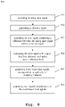
- a first step 801 an analog input signal is provided.
- a reference signal is generated.
- an error signal is generated that comprises a difference between the analog input signal and the reference signal.
- the error signal is compared with respect to a first reference level and to a second reference level.
- event-based reset signals are generated corresponding to a plurality of sampling instances.
- additional reset signals asynchronous to the event-based reset signals are generated.
- the embodiments of the present invention can be implemented by hardware, software, or any combination thereof.
- Various embodiments of the present invention may be implemented by one or more application specific integrated circuits (ASICs), digital signal processors (DSPs), digital signal processing devices (DSPDs), programmable logic devices (PLDs), field programmable gate arrays (FPGAs), processors, controllers, microcontrollers, microprocessors, or the like.
- ASICs application specific integrated circuits
- DSPs digital signal processors
- DSPDs digital signal processing devices
- PLDs programmable logic devices
- FPGAs field programmable gate arrays
- processors controllers, microcontrollers, microprocessors, or the like.
Landscapes
- Engineering & Computer Science (AREA)
- Theoretical Computer Science (AREA)
- Analogue/Digital Conversion (AREA)
Abstract
Description
- The invention relates to analog-to-digital signal conversion, especially to asynchronous analog-to-spike converter architectures in wireless sensor nodes.
- Generally, minimizing power consumption in wireless sensor nodes is important to ensure a long lifetime of the battery. One way to minimize the power consumption is by making the power consumption activity dependent. For many biological signals, such as ECG, EEG, neuron signals, only small pieces in time are important to process. This reduced data helps, for example, the transmitter, since it now needs to transmit less data and thus uses less power. Since the transmitter power consumption is usually much higher than other components such as the front-end, reducing the power of the transmitter has a significant impact on the total power consumption.
- For a continuous monitoring system, the analog information is continuously monitored by a front-end, then converted by an analog-to-digital converter (ADC), and then sent out via a transmitter. Conventionally, an ADC samples the signal at every clock pulse, which is independent of the input signal. This means that even when the signal does not change, samples are still being generated. A different way of sampling is called level-crossing sampling, where a sampling instance occurs, i.e. the generation of a sample, only when the amplitude of the signal changed by a fixed step. The patent document
US 9,252,658 B2 - Usually, two different comparators are used to compare against the reference level just above and below the signal level. However, the input referred offset of the comparators directly affects the achievable signal-to-noise-and-distortion ratio (SNDR). This means that to achieve high SNDR (e.g. > 60dB), the offset of the comparator must be kept low. Additionally, for low frequency, high SNR applications, the required area of a level-crossing ADC becomes very large. This is due to the leakage in typical CMOS technologies. To meet the long hold time requirement of the digital-to-analog converter (DAC) for low frequency signals, large capacitors are necessary. The large area becomes a problem when, for instance, thousands of channels in the human body are needed to measure bio signals.
- Accordingly, an object of the invention is to provide a system and a method for analog-to-digital signal conversion, which can address the above-mentioned limitations.
- The object is solved by the features of the first independent claim for the system and by the features of the second independent claim for the method. The dependent claims contain further developments.
- According to a first aspect of the invention, a system for analog-to-digital signal conversion is provided. The system comprises an analog input signal, a digital-to-analog converter configured to generate a reference signal, and an amplifier configured to amplify an error signal comprising a difference between the analog input signal and the reference signal. The system further comprises a level-crossing based sampling circuit comprising a first comparator configured to compare the error signal with respect to a first reference level, and a second comparator configured to compare the error signal with respect to a second reference level, thereby generating event-based reset signals corresponding to a plurality of sampling instances in order to reset the digital-to-analog converter and further to shift the first reference level and the second reference level through the digital-to-analog converter. Moreover, the system comprises a trigger circuit configured to generate reset signals asynchronous to the event-based reset signals in order to reset the digital-to-analog converter.
- Therefore, the invention proposes additional resets for resetting the DAC in addition to the event-based resets correspond to each sampling instances, i.e. to each instance of sample generation. Said event-based reset signals or spikes reset the DAC and further change the reference signal level (e.g. voltage level) through the DAC, especially by shifting the first reference level and the second reference level via the DAC. Furthermore, the resets are not clock-generated so as to eliminate the necessity of having on-board oscillators.
- Consequently, large area capacitors for the DAC are not required even if the signal changes slowly, since the additional resets minimize the requirements for a longer hold time. Moreover, the amplifier, or a so-called pre-amplifier, shared by the comparators solves the problem with the required area for the calibration of the comparators. Any error made after the pre-amplifier is divided by the gain of said pre-amplifier, thereby relaxing the offset requirement of the comparators.
- Preferably, the level-crossing based sampling circuit further comprises a digital logic circuit configured to generate an amplitude and a time stamp corresponding to each of the plurality of sampling instances. In addition, the digital logic circuit is further configured to feedback the amplitude corresponding to each of the plurality of sampling instances to the digital-to-analog converter in order to generate the reference signal. In this regard, the digital logic circuit may comprise an up/down counter that functions as a digital integrator and a timer that records the time in-between two sampling instances or samples. For each sampling instances, the output of the comparators toggles and the digital logic circuit starts to update the up/down counter to refresh the comparison window.
- Preferably, the digital-to-analog converter is a capacitive charge transfer digital-to-analog converter, more preferably a switched capacitor based digital-to-analog converter. In this regard, the trigger circuit comprises a switched capacitor arrangement in order to replicate the digital-to-analog converter. The use of capacitive DAC for reference signal or voltage generation advantageously facilitates smaller area and low power consumption. Moreover, by replicating the DAC, e.g. replicating the switched-capacitor arrangement of the DAC, the leakage induced error of the DAC can be potentially measured during operation.
- Preferably, the level-crossing based sampling circuit further comprises a first capacitor bank coupled between a common node downstream to the amplifier and the first comparator, where the first capacitor bank is configured to store the first reference level based on the reference signal. In addition, the level-crossing based sampling circuit further comprises a second capacitor bank coupled between the common node downstream to the amplifier and the second comparator, where the second capacitor bank is configured to store the second reference level based on the reference signal.
- Advantageously, only one pre-amplifier is used to store the reference levels, i.e. two references that are two LSB apart, in order to compare the input signal against said reference levels. This further reduces the overall area requirement of the ADC in addition to input referred offset compensation for the comparators.
- Preferably, the first capacitor bank and/or the second capacitor bank comprises a pair of parallel capacitors and switching arrangements. In this context, the switching arrangements are configured to be operable such that at least one capacitor of the pair of parallel capacitors stores a charge proportional to two least significant bit (LSB) in addition to an offset error of the amplifier. Furthermore, the switching arrangements are configured to be operable such that at least one capacitor of the pair of parallel capacitors stores a charge proportional to the offset error of the amplifier. Moreover, the switching arrangements are configured to be operable such that the pair of parallel capacitors each store a charge proportional to one least significant bit (LSB). This effectively provides two references that are two LSB apart for the ADC to compare the input signal against said references.
- Preferably, the pair of parallel capacitors of the first capacitor bank and/or the second capacitor bank are equal in dimension, preferably identical parallel plate capacitors. Further preferably, the digital logic circuit is configured to generate control signals for the switching arrangements of the first capacitor bank and/or the second capacitor bank. This advantageously provides a simple arrangement for storing the references.
- According to a second aspect of the invention, a method for signal conversion is provided in a system for analog-to-digital signal conversion. The method comprises the step of providing an analog input signal. The method further comprises the step of generating a reference signal by a digital-to-analog converter. In addition, the method comprises the step of generating an error signal comprising a difference between the analog input signal and the reference signal and amplifying the error signal by an amplifier. Furthermore, the method comprises the step of comparing the error signal with respect to a first reference level and a second reference level and generating event-based reset signals corresponding to a plurality of sampling instances by a level-crossing based sampling circuit. Moreover, the method further comprises the step of generating reset signals asynchronous to the event-based reset signals by a trigger circuit.
- Therefore, the invention proposes additional resets for resetting the DAC in addition to the event-based resets correspond to each sampling instances, i.e. to each instances of sample generation, which effectively minimize the requirements for a longer hold time of the DAC. Moreover, the offset requirements of the comparators are relaxed by the gain of the amplifier, which is shared by both comparators.
- Preferably, the method further comprises the step of providing a first capacitor bank comprising a pair of parallel capacitors and switching arrangements in order to store the first reference level and providing a second capacitor bank comprising a pair of parallel capacitors and switching arrangements in order to store the second reference level.
- Preferably, the method further comprises the step of operating the switching arrangements of the first capacitor bank and/or of the second capacitor bank for storing, by at least one capacitor of the pair of capacitors, a charge proportional to two least significant bit (LSB) in addition to an offset error of the amplifier, and for storing, by at least one capacitor of the pair of capacitors, a charge proportional to the offset error of the amplifier, and for storing, by each of the pair of capacitors, a charge proportional to one least significant bit (LSB). This effectively provides two references that are two LSB apart for the ADC to compare the input signal against said references.
- Exemplary embodiments of the invention are now further explained with respect to the drawings by way of example only, and not for limitation. In the drawings:
- Fig. 1A
- shows a conventional level-crossing based analog-to-digital converter;
- Fig. 1B
- shows exemplary sampling instances of the conventional level-crossing based analog-to-digital converter of
Fig. 1A ; - Fig. 2
- shows a first exemplary embodiment of the system according to the first aspect of the invention;
- Fig. 3A
- shows a first exemplary embodiment of the trigger circuit;
- Fig. 3B
- shows exemplary operation stages of the trigger circuit of
Fig. 3A ; - Fig. 4A
- shows the leakage induced error caused by a finite hold time of a digital-to-analog converter;
- Fig. 4B
- shows the mitigation technique for the leakage induced error caused by a finite hold time of a digital-to-analog converter;
- Fig. 5A
- shows a second exemplary embodiment of the trigger circuit;
- Fig. 5B
- shows exemplary output pulses of the trigger circuit of
Fig. 5A ; - Fig. 6
- shows exemplary switched-capacitor arrangements for storing the reference levels;
- Fig. 7
- shows a second exemplary embodiment of the system according to the first aspect of the invention; and
- Fig. 8
- shows an exemplary embodiment of the method according to the second aspect of the invention.
- Reference will now be made in detail to the embodiments of the present invention, examples of which are illustrated in the accompanying drawings. However, the following embodiments of the present invention may be variously modified and the range of the present invention is not limited by the following embodiments.
- Along
Fig. 1A and Fig. 1B , the operation of a conventional level-crossing based analog-to-digital converter is illustrated. Particularly,Fig. 1A shows a conventional level-crossing analog-to-digital converter (LC-ADC) that converts the analog signal Vin into discrete samples at a numerous sampling instances. Specifically, the LC-ADC uses level-crossing detection to sample the analog signal Vin. The LC-ADC consists of two comparators 104,105, a digital-to-analog converter (DAC) 101 and alogic block 106 comprising an up/down counter. Two threshold levels VH and VL are set to identify the analog signal Vin. The threshold levels VH and VL are generated via theDAC 101 with a difference equal to the quantization step. Hence, in digital representation, the difference between VH and VL is equal to 2 least significant bit (LSB). Theerror 102 between Vin and VH is fed to thecomparator 104 and theerror 103 between Vin and VL is fed to thecomparator 105 for comparison, for example. - The sampling instance or sampling occurs when Vin is either higher than VH or lower than VL. The
logic block 106 then sets an increment signal or a decrement signal accordingly to activate the up/down counter, thereby incrementing or decrementing the counter output by 1 LSB. This further controls theDAC 101 whose generated signals VH and VL will be updated to keep tracking the analog signal Vin. On the other hand, as long as the analog signal Vin is between VH and VL, no changes occur on the up/down counter output orDAC 101 output, therefore no new samples are taken. The sampling instances are further shown inFig. 1B , where the analog signal Vin is sampled at different instances, e.g. 107, based on asampling window 108 defined by the difference between VH and VL. - However, the two comparators 104,105 have a different offset voltage, which degrades the SNDR and therefore is required to be kept small in order to achieve a high SNDR. One possible solution is to add a foreground calibration, especially a resistive calibration DAC that can permanently hold the reference voltage. However, this solution comes with the cost of increased power consumption and further increases the overall area due to the requirement of an additional clock. Moreover, said calibration scheme is not able to counter offset drifts, which might hinder the performance in a real application.
- Using a capacitive DAC for the reference voltage generation is the most common architecture for LC-ADC due to its small area and power consumption. The problem with a capacitive DAC however is that it is not possible to hold the charge indefinitely. Since the
DAC 101 is only reset when the analog signal Vin crosses VH or VL, theDAC 101 is not reset when the analog signal Vin changes slowly. This results in the leakage induced error becoming large and therefore degrades the SNDR, especially for low frequencies. - In
Fig. 2 , a first exemplary embodiment of thesystem 200 according to the first aspect of the invention is illustrated. The system 200 (can also be referred to as an analog-to-digital converter) comprises ananalog input signal 201 to be converted into discrete samples while areference signal 203 is generated by a digital-to-analog converter (DAC) 202 for domain conversion. Theanalog input signal 201 and thereference signal 203 are summed at asubtractor 204, which results in an error or difference signal (voltage, charge or current) 205 comprising a difference between theanalog input signal 201 and thereference signal 203. Saiderror signal 205 is fed to an amplifier or apre-amplifier 206 that amplifies the error signal by the gain of theamplifier 206. Hence, theamplifier 206 advantageously mitigates any signal loss due to the subtraction of theanalog input signal 201 and thereference signal 203 at thesubtractor 204. - The
amplifier 206 provides acommon node 207 at its output, which commonly shares thecommon node 207 with afirst path 210 connecting to a non-inverting input of afirst comparator 214 and asecond path 211 connecting an inverting input of asecond comparator 215. Afirst capacitor bank 208 is located at thefirst path 210 between thecommon node 207 and the non-inverting input of thefirst comparator 214. Asecond capacitor bank 209 is located at thesecond path 211 between thecommon node 207 and the inverting input of thesecond comparator 215. An inverting input of thefirst comparator 214 and a non-inverting input of thesecond comparator 215 are commonly connected to ground. Thefirst capacitor bank 208 and thesecond capacitor bank 209 each comprise a pair of parallel capacitors (not shown) and switching arrangements, whose functionalities will be discussed in a later section of this description. - The
output 216 of thefirst comparator 214 and theoutput 217 of thesecond comparator 215 are connected to adigital logic circuit 218. Saiddigital logic circuit 218 is composed of but not limited to an up/down counter and a timer (e.g. time-to-digital converter). Thefirst capacitor bank 208, thesecond capacitor bank 209, thefirst comparator 214, thesecond comparator 215, and thedigital logic circuit 218 collectively form a level-crossing basedsampling circuit 220. The sampledoutput 219 from thedigital logic circuit 218 is fed back to theDAC 202 over afeedback path 222 in order to generate thereference signal 203. Thedigital logic circuit 218 further outputs event-based reset signals 221 for each sampling instance or samples (i.e. up/down event) in order to reset theDAC 202. - The system further comprises a triggering
arrangement 230 for resetting theDAC 202 in addition to the event-based reset signals 221. Said triggeringarrangement 230 comprises atrigger circuit 223 that generatesreset signals 224 asynchronous to the event-based reset signals 221. The triggeringarrangement 230 further comprises a two-input ORgate 225 that inputs the event-based reset signals 221 from thedigital logic circuit 218 and the trigger signals 224 from thetrigger circuit 224, thereby outputting atrigger signal 226 whenever either one or both of the inputs of theOR gate 225 is high. It is to be noted that theOR gate 225 can be implemented with any logical combinations or gates as long as the output of said combinations is high when either one or both of the inputs are high. - Generally, the
error signal 205 is amplified by theamplifier 206 and is further compared with a first reference level stored at thefirst capacitor bank 208 by thefirst comparator 214. Ideally, the first reference level gives the upper boundary of the comparison window. Similarly, theerror signal 205 is amplified by theamplifier 206 and is further compared with a second reference level stored at thesecond capacitor bank 209 by thesecond comparator 215. Ideally, the second reference level gives the lower boundary of the comparison window. The storing method of the reference levels at thefirst capacitor bank 208 and at thesecond capacitor bank 209 will be discussed later in detail. The event-based reset signals 221 from thedigital logic circuit 218 further change the reference signal level by shifting the first reference level and the second reference level via theDAC 202, thereby shifting the comparison window for subsequent comparisons. - In other words, the
first comparator 214 and thesecond comparator 215 respectively compare theerror signal 205 with respect to a fixed comparison window, i.e. in digital representation of 2 LSB, and toggles its output whenever it detects a level crossing. This result in the generation of respective sampling instances or samples and further toggles the up/down counter to generate an up or down event. Since thefirst comparator 214 and thesecond comparator 215 compare theerror signal 205 instead of theinput analog signal 201, the comparator common-mode range is reduced significantly and optimization of the comparators targeting at a specific reference level can be performed with ease. The related effects that result from comparator offset and distortion are thus reduced. More importantly, similar performance is achievable for the comparators with lower power consumption. - In addition, the
amplifier 206 is shared by thefirst comparator 214 and thesecond comparator 215. Thus, any error made after theamplifier 206 is divided by the gain of theamplifier 206, which relaxes the offset requirement of thefirst comparator 214 and thesecond comparator 215. - When the
first comparator 214 and/or thesecond comparator 215 detect a level crossing with respect to the comparison window, the output of thefirst comparator 214 and/or the output of thesecond comparator 215 toggle and thedigital control circuit 218 updates the up/down counter in order to refresh the comparison window, thereby resetting theDAC 202. Said up/down counter acts as a digital integrator and the time in between two sampling instances are recorded by the timer. - In addition to the up and/or down event-based reset signals 221, the
trigger circuit 223 further generates asynchronous trigger signals 224, which are cumulatively operating on theDAC 202 to reset theDAC 202, even when there is no sampling instances recorded at thedigital logic circuit 218. - Along
Fig. 3A and Fig. 3B , a first exemplary embodiment of the trigger circuit is illustrated. In particular,Fig. 3A shows thetrigger circuit 300, which can be implemented as thetrigger circuit 223 ofFig. 2 .Fig. 3B shows operation stages of saidtrigger circuit 300. - Preferably, the
DAC 202 is a capacitive DAC, and thetrigger circuit 300 is realized so that it replicates said capacitive DAC. Since the leakage cannot be directly measured in theDAC 202, thereplica circuit 300 is able to sense the leakage and further to act accordingly to mitigate the leakage. Thetrigger circuit 300 comprises acapacitor 301 connected to ground at one node and further provides a common port A to the other node. At the common node A, aNMOS switch 302 is coupled. Particularly, the drain of the NMOS switch is coupled to the common node A whereas the source of the NMOS switch is coupled to a node B. Asecond switch 304 is coupled to the node B that initially connects the node B to a bias voltage VDD. A comparator 303 is coupled to the common node A and the output OUT of thecomparator 303 is fed back to the gate of theNMOS switch 302 and further used to toggle thesecond switch 304 between the bias voltage VDD andground 305. - During normal operation, the output OUT is low. Due to leakage through the
NMOS switch 302, the voltage of thecapacitor 301 rises. When the voltage of thecapacitor 301 exceeds the trip point of thecomparator 303, the output OUT goes high. This causes theNMOS switch 302 to turn on and thesecond switch 304 to toggle toground 305. Thecapacitor 301 then discharges through theNMOS switch 302 and the voltage on the capacitor goes low again. This further sets the output OUT low and restarts the cycle. - The operation phases can be seen in
Fig. 3B where the OUT is initially low and the voltage at A is rising, i.e. the charging state of thecapacitor 301. The voltage at B is at VDD. When the voltage at A rises to the trip point of thecomparator 303, thecomparator 303 output toggles, and thus OUT becomes high. At this point thecapacitor 301 discharges and the voltage at A goes low as well as the voltage at B, since the latter is now connected to ground. This further sets the output OUT low and restarts the cycle. The OUT signals therefore represent the additional trigger signals 224 that are generated asynchronous to the event-based trigger signals 221 from the level-crossing basedsampling circuit 220. - Along
Fig. 4A and Fig. 4B , the leakage induced error of a digital-to-analog converter and the proposed mitigation technique are illustrated. Particularly,Fig. 4A shows the leakage induced error caused by a finite hold time of the digital-to-analog converter 202. As already mentioned before, a capacitive DAC is the most common architecture for the reference generation but suffers from a finite hold time. The signal Vin represents theanalog input signal 201 which is sampled along a sampling window provided by the upper boundary or first reference level VH and the lower boundary or second reference level VL. The event-based reset signals 221 are shown as spikes respective to each up/down events, i.e. sampling instances. - When the signal Vin changes sharply, more samples are generated, thereby generating more event-based reset signals 221. Hence, for fast changing signals, the drift in the reference is very short and therefore the leakage induced error is not significant. However, when the signal changes slowly, less number of samples are generated, thereby less number of event-based reset signals 221. This results in that the DAC reference drifts away and introduces a large leakage induced error. As it can be seen, the
DAC 202 resets atpoint 401 and further drifts at 402 and further resets at 403. Since the time between crossings is short, the leakage induced error is not significant. However, at 404, the DAC drifts for a longer time that introduces a large leakage induced error. -
Fig. 4B shows the proposed technique of having additional resets in order to mitigate the large leakage induced error in theDAC 202. Additional trigger signals 224 are generated along with the event-based reset signals 221, especially asynchronous to the event-based reset signals 221. Hence, when the signal Vin is changing slowly, e.g. at 405 theDAC 202 resets and further drifts at 406, however, is not drifting anymore due to theadditional resets 224. TheDAC 202 resets at 407 instead. As a result, a large portion of the leakage induced error is mitigated. - Along
Fig. 5A and Fig 5B , a second exemplary embodiment of the trigger circuit is illustrated. In particular,Fig. 5A shows thetrigger circuit 500, which can be implemented as thetrigger circuit 223 ofFig. 2 .Fig. 5B shows the output of saidtrigger circuit 500. - The requirements for an additional trigger generating circuit are very relaxed since exact timing is not required. Therefore, the
trigger circuit 223 can be implemented as a current starvedring oscillator circuit 500 as shown inFig. 5A . Thering oscillator 500 comprises afirst inverter stage 501, asecond inverter stage 502 and athird inverter stage 503, where theoutput 504 of thethird inverter stage 503 is fed back to thefirst inverter stage 501. Although three inverter stages are illustrated herein, it is to be noted that any odd number of inverter stages can be implemented as long as the total propagation delay, i.e. the frequency of oscillation, meets the target specification. Hence, by connecting together any odd number of inverters to form a ring circuit, and by connecting the output of the ring straight back to the input of the ring, the circuit will continue to oscillate as a logic level "1" constantly rotates around the network. The oscillating outputs OUT can be seen inFig. 5B , which represent the trigger signals 224 additionally generated to the event-based trigger signals 221. - In
Fig. 6 , thefirst capacitor bank 208 and thesecond capacitor bank 209 are shown in detail. It is to be noted that the implementation is illustrated as a single-ended implementation and it is applicable to both capacitor banks 208,209. Each capacitor bank comprises a pair ofparallel capacitors capacitors amplifier 206 output is connected to one end of thecapacitor 601 and the other end of thecapacitor 601 is connected to the switches S1 and S4, where the switch S1 can be toggled toground 603. On the other hand, the switch S2 is connected in parallel with thecapacitor 602 to the switch S4 and the switch S3 is connected in series with thecapacitor 602, where the switch S3 can be toggled toground 604. Thefirst path 210 and/or thesecond path 211, as shown inFig. 2 , is coupled at the parallel junction between the switch S4, the switch S2 and thecapacitor 602. - Along
Fig. 6 the steps or phases for storing the reference level at the respective capacitor bank are illustrated in detail. During a first phase or step, S1 is toggled toground 603, S4 is opened (i.e. no conduction through the switch), S2 is opened, and S3 is closed (i.e. conduction through the switch). During this phase, noinput analog signal 201 is inputted to thesubtractor 204 and theDAC 202 generates reference voltage corresponding to the digital representation of 2 least significant bit (LSB). Theamplifier 206 amplifies the 2LSB along with an input referred offset 600 of theamplifier 206 by the gain A. Therefore, the output of theamplifier 206 during the first phase is given as:
amplifier 206. - Since S4 is opened and S1 is grounded, the
capacitor 601 will store the charge equivalent to theamplifier 206 output.
capacitor 601, C is the capacitance of thecapacitor 601. The negative sign represents the change in the direction of the stored reference voltage, i.e. the polarity of thecapacitor 601 is reversed. - During a second phase or step, S1 is opened, S4 is kept open, however S2 is closed and S3 is connected to the
ground 604. During this phase no analog input signal as well as no reference signal are inputted to thesubtractor 204. Therefore, theamplifier 206 amplifies only the input referred offset 600 by the gain A. Hence, the output of theamplifier 206 during the second phase is given as:
- Since S2 is closed and S3 is grounded, the
capacitor 602 will store the charge equivalent to theamplifier 206 output.
capacitor 602, C is the capacitance of thecapacitor 602, similar to thecapacitor 601 as they are equally sized capacitors. Note that the signal is stored in the same direction of the amplifier output, therefore bearing no negative sign. Thus the polarity of thecapacitor 602 is opposite to the polarity of thecapacitor 601. - During a third phase or step, S1 is opened, S4 is closed, however S2 is opened and S3 is closed again. During this phase, the system performs the normal operation, i.e. the
analog input signal 201 and thereference signal 203 are inputted to thesubtractor 204. Thus, theamplifier 206 amplifies the difference or error signal along with the input referred offset 600. Hence, the output of theamplifier 206 during the third phase is given as:
- Where, Vin is the
analog input signal 201 and Vref is thereference signal 203 generated from theDAC 202. - However, since S4 is now closed, the
capacitors capacitor 
- Therefore, the respective comparators compare the output of the
amplifier 206 with respect to the reference level correspondingly stored at therespective capacitor banks digital logic circuit 218 provides the control signals require to toggle the switches S1, S2, S3 and S4, which can be generated from a sequence of logic based on the different phases described above and/or can be pre-programmed and further can be executed before and during the signal conversion. - In
Fig. 7 , a second exemplary embodiment of thesystem 700 according to the first aspect of the invention is illustrated. Thesystem 700 differs from thesystem 200 in that the reference levels are separately inputted through an additional amplifier as opposed to input via a shared amplifier and to store the reference levels in two capacitor banks. - The
system 700 comprises theanalog input signal 201 to be converted into discrete samples while thereference signal 203 is generated by theDAC 202 for domain conversion. Theanalog input signal 201 and thereference signal 203 are summed at thesubtractor 204, which results in the error or difference signal (voltage, charge or current) 205 comprising a difference between theanalog input signal 201 and thereference signal 203. Saiderror signal 205 is fed to the amplifier or thepre-amplifier 206 that amplifies the error signal by the gain of theamplifier 206. - The output of the
amplifier 206 is fed to the non-inverting input of thefirst comparator 214 and further to the inverting input of thesecond comparator 215. In addition, areference level 701 is inputted to anadditional amplifier 706, where the output of theamplifier 706 is fed to the inverting input of the first comparator and further to the non-inverting input of the second comparator, however the latter input is inverted by aninverter 708. Hence, theamplifier 206 provides theerror signal 205 whereas theamplifier 706 provides the reference levels for the comparison window. It is to be noted that theamplifier 706 is selected so as to match the gain of theamplifier 206. The level-crossing based sampling as well as the additional trigger generation as described alongFig. 2 are analogously performed in thesystem 700, and are not repeated herein. - In
Fig. 8 , an exemplary embodiment of themethod 800 according to the second aspect of the invention is illustrated. In afirst step 801, an analog input signal is provided. In asecond step 802, a reference signal is generated. In athird step 803, an error signal is generated that comprises a difference between the analog input signal and the reference signal. In afourth step 804, the error signal is compared with respect to a first reference level and to a second reference level. In afifth step 805, event-based reset signals are generated corresponding to a plurality of sampling instances. In asixth step 806, additional reset signals asynchronous to the event-based reset signals are generated. - The embodiments of the present invention can be implemented by hardware, software, or any combination thereof. Various embodiments of the present invention may be implemented by one or more application specific integrated circuits (ASICs), digital signal processors (DSPs), digital signal processing devices (DSPDs), programmable logic devices (PLDs), field programmable gate arrays (FPGAs), processors, controllers, microcontrollers, microprocessors, or the like.
- Although the invention has been illustrated and described with respect to one or more implementations, equivalent alterations and modifications will occur to others skilled in the art upon the reading and understanding of this specification and the annexed drawings. In addition, while a particular feature of the invention may have been disclosed with respect to only one of several implementations, such feature may be combined with one or more other features of the other implementations as may be desired and advantageous for any given or particular application.
Claims (15)
- A system (200) for analog-to-digital signal conversion comprising:an analog input signal (201),a digital-to-analog converter (202) configured to generate a reference signal (203),an amplifier (206) configured to amplify an error signal comprising a difference between the analog input signal (201) and the reference signal (203),a level-crossing based sampling circuit (220) comprising a first comparator (214) configured to compare the error signal with respect to a first reference level, and a second comparator (215) configured to compare the error signal with respect to a second reference level, thereby generating event-based reset signals (221) corresponding to a plurality of sampling instances in order to reset the digital-to-analog converter (202) and further to shift the first reference level and the second reference level through the digital-to-analog converter (202); anda trigger circuit (223) configured to generate reset signals (224) asynchronous to the event-based reset signals (221) in order to reset the digital-to-analog converter (202) .
- The system according to claim 1,
wherein the level-crossing based sampling circuit (210) further comprises a digital logic circuit (218) configured to generate an amplitude and a time stamp corresponding to each of the plurality of sampling instances. - The system according to claim 2,
wherein the digital logic circuit (218) is further configured to feedback the amplitude corresponding to each of the plurality of sampling instances to the digital-to-analog converter (202) in order to generate the reference signal (203). - The system according to any of claims 1 to 3,
wherein the digital-to-analog converter (202) is a capacitive charge transfer digital-to-analog converter, preferably a switched capacitor based digital-to-analog converter. - The system according to claim 4,
wherein the trigger circuit (223) comprises a switched capacitor arrangement (300) in order to replicate the digital-to-analog converter (202). - The system according to any of claims 1 to 5,
wherein the level-crossing based sampling circuit (220) further comprises a first capacitor bank (208) coupled between a common node (207) downstream to the amplifier (206) and the first comparator (214), where the first capacitor bank (208) is configured to store the first reference level based on the reference signal (203). - The system according to any of claims 1 to 6,
wherein the level-crossing based sampling circuit (220) further comprises a second capacitor bank (209) coupled between the common node (207) downstream to the amplifier (206) and the second comparator (205), where the second capacitor bank (209) is configured to store the second reference level based on the reference signal (203). - The system according to any of claims 1 to 7,
wherein the first capacitor bank (208) and/or the second capacitor bank (209) comprises a pair of parallel capacitors (601,602) and switching arrangements, wherein the switching arrangements are configured to be operable such that at least one capacitor of the pair of parallel capacitors (601,602) stores a charge proportional to two least significant bit "LSB" in addition to an offset error (600) of the amplifier (206). - The system according to claim 8,
wherein the switching arrangements are further configured to be operable such that at least one capacitor of the pair of parallel capacitors (601,602) stores a charge proportional to the offset error (600) of the amplifier (206) . - The system according to claim 8,
wherein the switching arrangements are further configured to be operable such that the pair of parallel capacitors (601,602) each stores a charge proportional to one least significant bit "LSB". - The system according to any of claims 1 to 10,
wherein the pair of parallel capacitors (601,602) of the first capacitor bank (208) and/or the second capacitor bank (209) are equal in dimension, preferably identical parallel plate capacitors. - The system according to any of claims 1 to 11,
wherein the digital logic circuit (218) is further configured to generate control signals for the switching arrangements of the first capacitor bank (208) and/or the second capacitor bank (208). - A method for analog-to-digital signal conversion comprising the steps of:providing an analog input signal (201);generating a reference signal (203) by a digital-to-analog converter (202);generating an error signal comprising a difference between the analog input signal (201) and the reference signal (203), and amplifying the error signal by an amplifier (206);comparing the error signal with respect to a first reference level and a second reference level, and generating event-based reset signals (221) corresponding to a plurality of sampling instances by a level-crossing based sampling circuit (220); andgenerating reset signals (224) asynchronous to the event-based reset signals (221) by a trigger circuit (223).
- The method according to claim 14,
wherein the method further comprises the step of providing a first capacitor bank (208) comprising a pair of parallel capacitors (601,602) and switching arrangements in order to store the first reference level and a second capacitor bank (209) comprising a pair of parallel capacitors (601,602) and switching arrangements in order to store the second reference level. - The method according to claim 14,
wherein the method further comprises the step of operating the switching arrangements of the first capacitor bank (208) and/or of the second capacitor bank (209) for:storing, by at least one capacitor of the pair of capacitors (601,602), a charge proportional to two least significant bit "LSB" in addition to an offset error (600) of the amplifier (206),storing, by at least one capacitor of the pair of capacitors (601,602), a charge proportional to the offset error (600) of the amplifier (206), and
storing, by each of the pair of capacitors (601,602), a charge proportional to one least significant bit "LSB".
Priority Applications (2)
| Application Number | Priority Date | Filing Date | Title |
|---|---|---|---|
| EP21150013.7A EP4024713B1 (en) | 2021-01-04 | 2021-01-04 | System and method for analog-to-digital signal conversion |
| US17/563,635 US11750206B2 (en) | 2021-01-04 | 2021-12-28 | System and method for analog-to-digital signal conversion |
Applications Claiming Priority (1)
| Application Number | Priority Date | Filing Date | Title |
|---|---|---|---|
| EP21150013.7A EP4024713B1 (en) | 2021-01-04 | 2021-01-04 | System and method for analog-to-digital signal conversion |
Publications (2)
| Publication Number | Publication Date |
|---|---|
| EP4024713A1 true EP4024713A1 (en) | 2022-07-06 |
| EP4024713B1 EP4024713B1 (en) | 2025-11-26 |
Family
ID=74095716
Family Applications (1)
| Application Number | Title | Priority Date | Filing Date |
|---|---|---|---|
| EP21150013.7A Active EP4024713B1 (en) | 2021-01-04 | 2021-01-04 | System and method for analog-to-digital signal conversion |
Country Status (2)
| Country | Link |
|---|---|
| US (1) | US11750206B2 (en) |
| EP (1) | EP4024713B1 (en) |
Families Citing this family (2)
| Publication number | Priority date | Publication date | Assignee | Title |
|---|---|---|---|---|
| WO2024226728A1 (en) * | 2023-04-25 | 2024-10-31 | Trustees Of Tufts College | Adaptive level crossing adc with machine learning |
| EP4730657A1 (en) * | 2024-10-16 | 2026-04-22 | Imec VZW | A reference-less level-crossing adc with a bump-based adaptive-bias comparator |
Citations (2)
| Publication number | Priority date | Publication date | Assignee | Title |
|---|---|---|---|---|
| US9252658B2 (en) | 2011-10-14 | 2016-02-02 | Massachusetts Institute Of Technology | Level-crossing based circuit and method with offset voltage cancellation |
| US20200160186A1 (en) * | 2018-11-20 | 2020-05-21 | Cirrus Logic International Semiconductor Ltd. | Inference system |
Family Cites Families (12)
| Publication number | Priority date | Publication date | Assignee | Title |
|---|---|---|---|---|
| GB9827932D0 (en) * | 1998-12-19 | 1999-02-10 | Secr Defence | Analogue to digital converter and method of analogue to digital conversion |
| US6353404B1 (en) * | 1999-05-07 | 2002-03-05 | Yamaha Corporation | D/A conversion apparatus and D/A conversion method |
| US6667702B2 (en) * | 2001-04-27 | 2003-12-23 | Rohm Co., Ltd | Semiconductor device having DACs and method of testing such semiconductor device |
| US7068203B2 (en) * | 2003-12-31 | 2006-06-27 | Texas Instruments Incorporated | Switched-capacitor circuits with reduced finite-gain effect |
| KR101252331B1 (en) | 2006-03-21 | 2013-04-08 | 캠브리지 아날로그 테크놀로지스, 인크. | Offset cancellation for sampled-data circuits |
| US8606051B2 (en) * | 2010-08-16 | 2013-12-10 | SK Hynix Inc. | Frame-wise calibration of column-parallel ADCs for image sensor array applications |
| US9203422B2 (en) * | 2011-09-29 | 2015-12-01 | Ecole Polytechique Federale De Lausanne (Epfl) | Low distortion switched-capacitor event-driven analog to digital converter |
| US8604861B1 (en) * | 2012-06-19 | 2013-12-10 | Infineon Technologies Ag | System and method for a switched capacitor circuit |
| GB2529686A (en) * | 2014-08-29 | 2016-03-02 | Ibm | High-speed comparator for analog-to-digital converter |
| US9806552B2 (en) * | 2016-02-15 | 2017-10-31 | Analog Devices Global | Analog/digital converter with charge rebalanced integrator |
| US10061272B2 (en) * | 2016-06-12 | 2018-08-28 | Board Of Regents, The University Of Texas System | Pipelined SAR ADC using comparator as a voltage-to-time converter with multi-bit second stage |
| US20210376844A1 (en) * | 2020-06-02 | 2021-12-02 | Short Circuit Technologies Llc | Event Driven Quasi-Level Crossing Delta Modulator Analog To Digital Converter With Adaptive Resolution |
-
2021
- 2021-01-04 EP EP21150013.7A patent/EP4024713B1/en active Active
- 2021-12-28 US US17/563,635 patent/US11750206B2/en active Active
Patent Citations (2)
| Publication number | Priority date | Publication date | Assignee | Title |
|---|---|---|---|---|
| US9252658B2 (en) | 2011-10-14 | 2016-02-02 | Massachusetts Institute Of Technology | Level-crossing based circuit and method with offset voltage cancellation |
| US20200160186A1 (en) * | 2018-11-20 | 2020-05-21 | Cirrus Logic International Semiconductor Ltd. | Inference system |
Non-Patent Citations (4)
| Title |
|---|
| RAVANSHAD NASSIM ET AL: "A fully-synchronous offset-insensitive level-crossing analog-to-digital converter", 2016 IEEE 59TH INTERNATIONAL MIDWEST SYMPOSIUM ON CIRCUITS AND SYSTEMS (MWSCAS), IEEE, 16 October 2016 (2016-10-16), pages 1 - 4, XP033073066, [retrieved on 20170302], DOI: 10.1109/MWSCAS.2016.7870108 * |
| TEMAN ADAM ET AL: "Replica Technique for Adaptive Refresh Timing of Gain-Cell-Embedded DRAM", IEEE TRANSACTIONS ON CIRCUITS AND SYSTEMS II: EXPRESS BRIEFS, IEEE, US, vol. 61, no. 4, 1 April 2014 (2014-04-01), pages 259 - 263, XP011545643, ISSN: 1549-7747, [retrieved on 20140415], DOI: 10.1109/TCSII.2014.2305016 * |
| TRAKIMAS M ET AL: "A 0.8 V asynchronous ADC for energy constrained sensing applications", CUSTOM INTEGRATED CIRCUITS CONFERENCE, 2008. CICC 2008. IEEE, IEEE, PISCATAWAY, NJ, USA, 21 September 2008 (2008-09-21), pages 173 - 176, XP031361437, ISBN: 978-1-4244-2018-6 * |
| WELTIN-WU COLIN ET AL: "An Event-driven Clockless Level-Crossing ADC With Signal-Dependent Adaptive Resolution", IEEE JOURNAL OF SOLID-STATE CIRCUITS, IEEE, USA, vol. 48, no. 9, 1 September 2013 (2013-09-01), pages 2180 - 2190, XP011524488, ISSN: 0018-9200, [retrieved on 20130821], DOI: 10.1109/JSSC.2013.2262738 * |
Also Published As
| Publication number | Publication date |
|---|---|
| EP4024713B1 (en) | 2025-11-26 |
| US11750206B2 (en) | 2023-09-05 |
| US20220216879A1 (en) | 2022-07-07 |
Similar Documents
| Publication | Publication Date | Title |
|---|---|---|
| US7068203B2 (en) | Switched-capacitor circuits with reduced finite-gain effect | |
| US10061272B2 (en) | Pipelined SAR ADC using comparator as a voltage-to-time converter with multi-bit second stage | |
| JP5558566B2 (en) | A / D converter and method for converting an analog input signal to a digital output | |
| US11784653B2 (en) | Hybrid analog-to-digital converter | |
| US20130335131A1 (en) | System and Method for a Switched Capacitor Circuit | |
| Wang et al. | An event-driven quasi-level-crossing delta modulator based on residue quantization | |
| US7773010B2 (en) | A/D converter comprising a voltage comparator device | |
| US7986257B2 (en) | Comparator circuit and analog digital converter having the same | |
| US11750206B2 (en) | System and method for analog-to-digital signal conversion | |
| de La Fuente-Cortes et al. | A new CMOS comparator robust to process and temperature variations for SAR ADC converters | |
| EP1678831B1 (en) | A dual residue pipelined ad converter | |
| Cenci et al. | A 28 nm 2 GS/s 5-b single-channel SAR ADC with gm-boosted StrongARM comparator | |
| Nasrollahpour et al. | Low power comparator with offset cancellation technique for Flash ADC | |
| Perczak et al. | An 800 kS/s 1.83 fJ/conv. 12b ADC via voltage successive approximation and gated cyclic vernier time digitization | |
| US12107596B2 (en) | Successive approximation register based time-to-digital converter using a time difference amplifier | |
| Keramat et al. | A capacitor mismatch and gain insensitive 1.5-bit/stage pipelined A/D converter | |
| Park et al. | All-digital ΔΣ time-to-digital converter with Bi-Directional gated delay line time integrator | |
| Kolte et al. | A review on successive approximation ADC | |
| Verbruggen | Digitally assisted analog to digital converters | |
| Chatterjee et al. | A low power offset voltage calibration method for flash ADCs | |
| Tong et al. | The influence of comparator offset on event-driven level-crossing analog-to-digital converter | |
| Kardonik | A study of SAR ADC and implementation of 10-bit asynchronous design | |
| KR102639792B1 (en) | Random Number Generator Based on Chaos in Time Domain | |
| Siddiqui et al. | 12 bit 3.072 GS/s 32‐way time‐interleaved pipelined ADC with digital background calibration for wideband fully digital receiver application in 65 nm complementary metal–oxide–semiconductor | |
| US20250279721A1 (en) | Method and system for buffering a reference voltage |
Legal Events
| Date | Code | Title | Description |
|---|---|---|---|
| PUAI | Public reference made under article 153(3) epc to a published international application that has entered the european phase |
Free format text: ORIGINAL CODE: 0009012 |
|
| STAA | Information on the status of an ep patent application or granted ep patent |
Free format text: STATUS: THE APPLICATION HAS BEEN PUBLISHED |
|
| AK | Designated contracting states |
Kind code of ref document: A1 Designated state(s): AL AT BE BG CH CY CZ DE DK EE ES FI FR GB GR HR HU IE IS IT LI LT LU LV MC MK MT NL NO PL PT RO RS SE SI SK SM TR |
|
| STAA | Information on the status of an ep patent application or granted ep patent |
Free format text: STATUS: REQUEST FOR EXAMINATION WAS MADE |
|
| 17P | Request for examination filed |
Effective date: 20221219 |
|
| RBV | Designated contracting states (corrected) |
Designated state(s): AL AT BE BG CH CY CZ DE DK EE ES FI FR GB GR HR HU IE IS IT LI LT LU LV MC MK MT NL NO PL PT RO RS SE SI SK SM TR |
|
| RIC1 | Information provided on ipc code assigned before grant |
Ipc: H03M 1/12 20060101AFI20250703BHEP Ipc: H03M 1/50 20060101ALI20250703BHEP Ipc: H03M 1/48 20060101ALI20250703BHEP Ipc: H03M 1/06 20060101ALN20250703BHEP |
|
| GRAP | Despatch of communication of intention to grant a patent |
Free format text: ORIGINAL CODE: EPIDOSNIGR1 |
|
| STAA | Information on the status of an ep patent application or granted ep patent |
Free format text: STATUS: GRANT OF PATENT IS INTENDED |
|
| INTG | Intention to grant announced |
Effective date: 20250819 |
|
| GRAS | Grant fee paid |
Free format text: ORIGINAL CODE: EPIDOSNIGR3 |
|
| GRAA | (expected) grant |
Free format text: ORIGINAL CODE: 0009210 |
|
| STAA | Information on the status of an ep patent application or granted ep patent |
Free format text: STATUS: THE PATENT HAS BEEN GRANTED |
|
| AK | Designated contracting states |
Kind code of ref document: B1 Designated state(s): AL AT BE BG CH CY CZ DE DK EE ES FI FR GB GR HR HU IE IS IT LI LT LU LV MC MK MT NL NO PL PT RO RS SE SI SK SM TR |
|
| REG | Reference to a national code |
Ref country code: CH Ref legal event code: F10 Free format text: ST27 STATUS EVENT CODE: U-0-0-F10-F00 (AS PROVIDED BY THE NATIONAL OFFICE) Effective date: 20251126 Ref country code: GB Ref legal event code: FG4D |
|
| REG | Reference to a national code |
Ref country code: IE Ref legal event code: FG4D |
|
| REG | Reference to a national code |
Ref country code: DE Ref legal event code: R096 Ref document number: 602021042890 Country of ref document: DE |
|
| P01 | Opt-out of the competence of the unified patent court (upc) registered |
Free format text: CASE NUMBER: UPC_APP_0004245_4024713/2026 Effective date: 20260205 |
|
| REG | Reference to a national code |
Ref country code: NL Ref legal event code: MP Effective date: 20251126 |
|
| PG25 | Lapsed in a contracting state [announced via postgrant information from national office to epo] |
Ref country code: ES Free format text: LAPSE BECAUSE OF FAILURE TO SUBMIT A TRANSLATION OF THE DESCRIPTION OR TO PAY THE FEE WITHIN THE PRESCRIBED TIME-LIMIT Effective date: 20251126 |
|
| REG | Reference to a national code |
Ref country code: LT Ref legal event code: MG9D |
|
| PG25 | Lapsed in a contracting state [announced via postgrant information from national office to epo] |
Ref country code: NO Free format text: LAPSE BECAUSE OF FAILURE TO SUBMIT A TRANSLATION OF THE DESCRIPTION OR TO PAY THE FEE WITHIN THE PRESCRIBED TIME-LIMIT Effective date: 20260226 |
|
| PGFP | Annual fee paid to national office [announced via postgrant information from national office to epo] |
Ref country code: DE Payment date: 20251217 Year of fee payment: 6 |
|
| PG25 | Lapsed in a contracting state [announced via postgrant information from national office to epo] |
Ref country code: FI Free format text: LAPSE BECAUSE OF FAILURE TO SUBMIT A TRANSLATION OF THE DESCRIPTION OR TO PAY THE FEE WITHIN THE PRESCRIBED TIME-LIMIT Effective date: 20251126 Ref country code: AT Free format text: LAPSE BECAUSE OF FAILURE TO SUBMIT A TRANSLATION OF THE DESCRIPTION OR TO PAY THE FEE WITHIN THE PRESCRIBED TIME-LIMIT Effective date: 20251126 Ref country code: HR Free format text: LAPSE BECAUSE OF FAILURE TO SUBMIT A TRANSLATION OF THE DESCRIPTION OR TO PAY THE FEE WITHIN THE PRESCRIBED TIME-LIMIT Effective date: 20251126 |
|
| REG | Reference to a national code |
Ref country code: AT Ref legal event code: MK05 Ref document number: 1862158 Country of ref document: AT Kind code of ref document: T Effective date: 20251126 |
|
| PG25 | Lapsed in a contracting state [announced via postgrant information from national office to epo] |
Ref country code: NL Free format text: LAPSE BECAUSE OF FAILURE TO SUBMIT A TRANSLATION OF THE DESCRIPTION OR TO PAY THE FEE WITHIN THE PRESCRIBED TIME-LIMIT Effective date: 20251126 |
|
| PG25 | Lapsed in a contracting state [announced via postgrant information from national office to epo] |
Ref country code: RS Free format text: LAPSE BECAUSE OF FAILURE TO SUBMIT A TRANSLATION OF THE DESCRIPTION OR TO PAY THE FEE WITHIN THE PRESCRIBED TIME-LIMIT Effective date: 20260226 |
|
| PG25 | Lapsed in a contracting state [announced via postgrant information from national office to epo] |
Ref country code: IS Free format text: LAPSE BECAUSE OF FAILURE TO SUBMIT A TRANSLATION OF THE DESCRIPTION OR TO PAY THE FEE WITHIN THE PRESCRIBED TIME-LIMIT Effective date: 20260326 |
|
| PG25 | Lapsed in a contracting state [announced via postgrant information from national office to epo] |
Ref country code: PT Free format text: LAPSE BECAUSE OF FAILURE TO SUBMIT A TRANSLATION OF THE DESCRIPTION OR TO PAY THE FEE WITHIN THE PRESCRIBED TIME-LIMIT Effective date: 20260326 |
|
| PG25 | Lapsed in a contracting state [announced via postgrant information from national office to epo] |
Ref country code: PL Free format text: LAPSE BECAUSE OF FAILURE TO SUBMIT A TRANSLATION OF THE DESCRIPTION OR TO PAY THE FEE WITHIN THE PRESCRIBED TIME-LIMIT Effective date: 20251126 |
|
| PG25 | Lapsed in a contracting state [announced via postgrant information from national office to epo] |
Ref country code: LV Free format text: LAPSE BECAUSE OF FAILURE TO SUBMIT A TRANSLATION OF THE DESCRIPTION OR TO PAY THE FEE WITHIN THE PRESCRIBED TIME-LIMIT Effective date: 20251126 |
|
| PG25 | Lapsed in a contracting state [announced via postgrant information from national office to epo] |
Ref country code: BG Free format text: LAPSE BECAUSE OF FAILURE TO SUBMIT A TRANSLATION OF THE DESCRIPTION OR TO PAY THE FEE WITHIN THE PRESCRIBED TIME-LIMIT Effective date: 20251126 |