EP4024677A1 - Anti-rotation feature for bonded stud - Google Patents
Anti-rotation feature for bonded stud Download PDFInfo
- Publication number
- EP4024677A1 EP4024677A1 EP21217839.6A EP21217839A EP4024677A1 EP 4024677 A1 EP4024677 A1 EP 4024677A1 EP 21217839 A EP21217839 A EP 21217839A EP 4024677 A1 EP4024677 A1 EP 4024677A1
- Authority
- EP
- European Patent Office
- Prior art keywords
- housing
- center stud
- recited
- assembly
- diode
- Prior art date
- Legal status (The legal status is an assumption and is not a legal conclusion. Google has not performed a legal analysis and makes no representation as to the accuracy of the status listed.)
- Pending
Links
Images



Classifications
-
- H—ELECTRICITY
- H02—GENERATION; CONVERSION OR DISTRIBUTION OF ELECTRIC POWER
- H02K—DYNAMO-ELECTRIC MACHINES
- H02K11/00—Structural association of dynamo-electric machines with electric components or with devices for shielding, monitoring or protection
- H02K11/04—Structural association of dynamo-electric machines with electric components or with devices for shielding, monitoring or protection for rectification
- H02K11/042—Rectifiers associated with rotating parts, e.g. rotor cores or rotary shafts
-
- H—ELECTRICITY
- H02—GENERATION; CONVERSION OR DISTRIBUTION OF ELECTRIC POWER
- H02K—DYNAMO-ELECTRIC MACHINES
- H02K5/00—Casings; Enclosures; Supports
- H02K5/04—Casings or enclosures characterised by the shape, form or construction thereof
-
- H—ELECTRICITY
- H02—GENERATION; CONVERSION OR DISTRIBUTION OF ELECTRIC POWER
- H02K—DYNAMO-ELECTRIC MACHINES
- H02K5/00—Casings; Enclosures; Supports
- H02K5/04—Casings or enclosures characterised by the shape, form or construction thereof
- H02K5/20—Casings or enclosures characterised by the shape, form or construction thereof with channels or ducts for flow of cooling medium
-
- H—ELECTRICITY
- H02—GENERATION; CONVERSION OR DISTRIBUTION OF ELECTRIC POWER
- H02K—DYNAMO-ELECTRIC MACHINES
- H02K7/00—Arrangements for handling mechanical energy structurally associated with dynamo-electric machines, e.g. structural association with mechanical driving motors or auxiliary dynamo-electric machines
- H02K7/003—Couplings; Details of shafts
-
- H—ELECTRICITY
- H10—SEMICONDUCTOR DEVICES; ELECTRIC SOLID-STATE DEVICES NOT OTHERWISE PROVIDED FOR
- H10D—INORGANIC ELECTRIC SEMICONDUCTOR DEVICES
- H10D62/00—Semiconductor bodies, or regions thereof, of devices having potential barriers
- H10D62/80—Semiconductor bodies, or regions thereof, of devices having potential barriers characterised by the materials
- H10D62/83—Semiconductor bodies, or regions thereof, of devices having potential barriers characterised by the materials being Group IV materials, e.g. B-doped Si or undoped Ge
- H10D62/8303—Diamond
-
- H—ELECTRICITY
- H10—SEMICONDUCTOR DEVICES; ELECTRIC SOLID-STATE DEVICES NOT OTHERWISE PROVIDED FOR
- H10D—INORGANIC ELECTRIC SEMICONDUCTOR DEVICES
- H10D8/00—Diodes
-
- H—ELECTRICITY
- H10—SEMICONDUCTOR DEVICES; ELECTRIC SOLID-STATE DEVICES NOT OTHERWISE PROVIDED FOR
- H10D—INORGANIC ELECTRIC SEMICONDUCTOR DEVICES
- H10D8/00—Diodes
- H10D8/01—Manufacture or treatment
-
- H—ELECTRICITY
- H10—SEMICONDUCTOR DEVICES; ELECTRIC SOLID-STATE DEVICES NOT OTHERWISE PROVIDED FOR
- H10D—INORGANIC ELECTRIC SEMICONDUCTOR DEVICES
- H10D8/00—Diodes
- H10D8/01—Manufacture or treatment
- H10D8/051—Manufacture or treatment of Schottky diodes
-
- H—ELECTRICITY
- H10—SEMICONDUCTOR DEVICES; ELECTRIC SOLID-STATE DEVICES NOT OTHERWISE PROVIDED FOR
- H10D—INORGANIC ELECTRIC SEMICONDUCTOR DEVICES
- H10D84/00—Integrated devices formed in or on semiconductor substrates that comprise only semiconducting layers, e.g. on Si wafers or on GaAs-on-Si wafers
- H10D84/201—Integrated devices formed in or on semiconductor substrates that comprise only semiconducting layers, e.g. on Si wafers or on GaAs-on-Si wafers characterised by the integration of only components covered by H10D1/00 or H10D8/00, e.g. RLC circuits
- H10D84/204—Integrated devices formed in or on semiconductor substrates that comprise only semiconducting layers, e.g. on Si wafers or on GaAs-on-Si wafers characterised by the integration of only components covered by H10D1/00 or H10D8/00, e.g. RLC circuits of combinations of diodes or capacitors or resistors
- H10D84/221—Integrated devices formed in or on semiconductor substrates that comprise only semiconducting layers, e.g. on Si wafers or on GaAs-on-Si wafers characterised by the integration of only components covered by H10D1/00 or H10D8/00, e.g. RLC circuits of combinations of diodes or capacitors or resistors of only diodes
-
- H—ELECTRICITY
- H10—SEMICONDUCTOR DEVICES; ELECTRIC SOLID-STATE DEVICES NOT OTHERWISE PROVIDED FOR
- H10W—GENERIC PACKAGES, INTERCONNECTIONS, CONNECTORS OR OTHER CONSTRUCTIONAL DETAILS OF DEVICES COVERED BY CLASS H10
- H10W90/00—Package configurations
Definitions
- the present disclosure relates to diode packs for electrical machines, and more particularly to anti-rotation features for studs in diode packs.
- Diode packs for electrical machines such as generators, motors, and motor/generators include conductive studs.
- conductive studs For example, there may be five radial studs and one center stud for electrical connection between the diodes within the diode pack and external devices. It has been typical to mold the center stud and radial studs into a polymeric pack housing, so that polymer of the housing insulates the radial studs from the center stud. This has generally been sufficient for its intended purpose; however, there is a limit in this technique to certain form factors wherein the gap between the center stud and radial studs is too small for an adequate amount of polymer to flow there between during the molding process.
- a diode pack comprises a plurality of diodes seated in an assembly within a housing.
- the diode pack also includes a plurality of radial studs extending from an axial end of the housing relative to an axis of rotation extending through the housing.
- Each of the radial studs is electrically connected to a respective diode within the assembly.
- the diode pack further includes a center stud captured within the housing between the assembly and the housing and along the axis of rotation.
- the center stud is electrically connected to the assembly as an electrical contact for the assembly.
- the housing electrically insulates between the center stud and each of the radial studs.
- a layer of adhesive can separate between the housing and the center stud.
- the diode pack can also include at least one Bellville washer within the housing, biasing the center stud in an axial direction against the housing.
- the diode pack can include a through tube in an axial end of the housing opposite the center stud and radial studs.
- the through tube can include a fluid passage in fluid communication with an interior space of the housing for flow of coolant in thermal contact with the assembly.
- the center stud can include a plurality of inlet openings for communication of fluid between the interior space and an interior flow passage of the center stud.
- the center stud can also include a plurality of outlet openings in fluid communication with at least one fluid passage extending radially through the housing for communication of fluid between the interior flow passage of the center stud and an exterior of the housing.
- the diode pack can include an end plate mounted to the axial end of the housing proximate the radial and center studs and additionally can include a sleeve seated about the housing, sealed to the housing by a plurality of O-rings.
- the housing can be operatively connected to a rotor shaft of an electrical machine.
- An axial end of the center stud can be captured in a double D-shaped feature defined in the axial end of the housing to prevent relative rotation of the housing and the center stud.
- a method of making a diode pack includes forming a housing of an electrically insulate material, removing a portion of the housing along an axis of rotation of the housing, mounting a center stud in the housing where the portion was removed, and assembling an assembly of diodes into the housing.
- mounting the center stud in the housing can include using an adhesive at least temporarily to hold the center stud in place during assembly. Further, mounting the center stud in the housing can also include capturing the center stud axially between the housing and the assembly of diodes. Mounting the center stud in the housing can include capturing the center stud circumferentially with a double-D shaped feature defined in the an axial end of the housing to prevent relative rotation of the housing and the center stud.
- forming a housing can include molding the housing. Forming the housing can include molding a plurality of radial studs in an axial end of the housing.
- a side cross-sectional view an embodiment of a diode pack in accordance with the disclosure is shown in Fig. 1 and is designated generally by reference character 100.
- Other embodiments of systems in accordance with the disclosure, or aspects thereof, are provided in Figs. 2-6 , as will be described.
- the systems and methods described herein can be used to provide anti-rotation features within a diode pack when used in an electrical machine.
- a diode pack 100 comprises a plurality of diodes 102 seated in an assembly 104 within a housing 106.
- the diode assembly 104 can include at least one diode 102, or six diodes 102 as shown, however any suitable number of diodes 102 can be included in the diode assembly 104.
- the diode pack 100 can include at least one radial stud 108, or a plurality of radial studs 108 as shown.
- the total number of radial studs 108 can include five radial studs 108 a,b,c,d,e, however any suitable number may be used.
- the radial studs 108 can extend from an axial end 110 of the housing 106 relative to an axis of rotation A, where the axis of rotation A extends through the housing 106.
- Each of the radial studs 108 can be electrically connected to a respective diode 102a,b,c,d,e,f within the assembly 104.
- bushings 150 can provide the electrical contacts between the radial studs 108 and respective diodes 102.
- the diode pack 100 can also include a center stud 112 captured within the housing 106 between the diode assembly 104 and the housing 106 and along the axis of rotation A.
- the center stud 112 can also be electrically connected to the diode assembly 104 as an electrical contact for the diode assembly 104.
- a non-conductive barrier 152 (e.g. labeled in Fig.
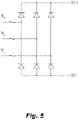
- FIG. 5 provides a schematic circuit diagram showing the electrical connection of the diodes 102a,b,c,d,e,f, within the diode assembly 104.
- the diode pack 100 can also include at least one Bellville washer 116 within the housing 106.
- the Bellville washer 116 is placed so as to bias the center stud 112 in an axial direction (e.g. along axis A) against the housing 106.
- the diode pack 100 can include a through tube 118 in an axial end 120 of the housing opposite the center stud 112 and radial studs 108.
- the through tube 118 can include a fluid passage 122 in fluid communication with an interior space 124 of the housing 106. In operation, the through tube 118 allows flow of coolant to flow through the fluid passage 122 and into the interior space 124 of the housing 106 and in thermal contact with the diode assembly 104.
- the diode pack 100 can include an end plate 136 mounted to the axial end 110 of the housing 106 proximate the radial and center studs 108, 112 and additionally can include a sleeve 138 seated about the housing 106.
- the sleeve 138 can be sealed to the housing 106 by a plurality of O-rings 140 as shown, or by any other suitable method.
- the center stud 112 can include a plurality of inlet openings 126 for communication of fluid between the interior space 124 and an interior flow passage 128 of the center stud 112.
- the center stud 112 can also include a plurality of outlet openings 130 in fluid communication with at least one fluid passage 132 extending radially through the housing 106 for communication of fluid between the interior flow passage 128 of the center stud 112 and an exterior of the housing 134.
- the inlet openings 126 and outlet openings 130 are placed circumferentially around the center stud 112. However, any suitable placement of the inlet and outlet openings 126, 130 can be used, as well as any suitable number of inlet and outlet openings 126, 130.
- the housing 106 can be operatively connected to a rotor shaft 142 of an electrical machine 144, for example as shown schematically in Fig. 1 .
- a layer of adhesive 114 can separate between the housing 106 and the center stud 112 (e.g. as shown in Fig. 3 ).
- the radial stud 112 may be inserted into the housing 106 with an adhesive layer 114 to prohibit rotation of housing 106 and center stud 112 when connected to an electrical machine.
- the adhesive layer 114 may fail, thus additional anti-rotation features may be included, such as a double-D shaped feature 148. As best seen in Fig.
- an axial end 146 of the center stud 112 can be captured in a double D-shaped feature 148.
- the double-D shaped feature 148 can be defined in the axial end 110 of the housing 106 to prevent relative rotation of the housing 106 and the center stud 112.
- a method 200 of making a diode pack includes, e.g. at box 202, forming a housing 106 of an electrically insulate material.
- the electrically insulate material can be any suitable non-conductive material as appreciated by those skilled in the art.
- forming the housing 106 can include molding (e.g. injection molding) the housing 106, such as shown at box 204, and forming the housing 106 can include molding a plurality of radial studs 108 in an axial end 110 of the housing 106, such as shown at box 206.
- the method 200 can include removing (e.g.
- the method 200 can include mounting a center stud 112 in the housing 106 where the portion was removed. Further, the method 200 can also include assembling an assembly of diodes 104 into the housing 106, shown at box 212.
- mounting the center stud 112 in the housing 106 can optionally include using an adhesive 114 at least temporarily to hold the center stud 112 in place during assembly, such as that shown at box 214.
- mounting the center stud 112 in the housing 106 can also include capturing the center stud 112 axially between the housing 106 and the assembly of diodes 104, e.g. as shown at box 216.
- mounting the center stud 112 in the housing 106 can include capturing the center stud 112 circumferentially with a double-D shaped feature 148, e.g. shown at box 218.
- the double-D shaped feature 148 can be defined in an axial end 110 of the housing 106 to prevent relative rotation of the housing 106 and the center stud 112.
Landscapes
- Engineering & Computer Science (AREA)
- Power Engineering (AREA)
Abstract
Description
- The present disclosure relates to diode packs for electrical machines, and more particularly to anti-rotation features for studs in diode packs.
- Diode packs for electrical machines such as generators, motors, and motor/generators include conductive studs. For example, there may be five radial studs and one center stud for electrical connection between the diodes within the diode pack and external devices. It has been typical to mold the center stud and radial studs into a polymeric pack housing, so that polymer of the housing insulates the radial studs from the center stud. This has generally been sufficient for its intended purpose; however, there is a limit in this technique to certain form factors wherein the gap between the center stud and radial studs is too small for an adequate amount of polymer to flow there between during the molding process.
- The conventional techniques have been considered satisfactory for their intended purpose. However, there is an ever present need for improved systems and methods for providing anti-rotation features in a diode pack while maintaining smaller housing form factors. This disclosure provides a solution for this need.
- A diode pack comprises a plurality of diodes seated in an assembly within a housing. The diode pack also includes a plurality of radial studs extending from an axial end of the housing relative to an axis of rotation extending through the housing. Each of the radial studs is electrically connected to a respective diode within the assembly. The diode pack further includes a center stud captured within the housing between the assembly and the housing and along the axis of rotation. The center stud is electrically connected to the assembly as an electrical contact for the assembly. The housing electrically insulates between the center stud and each of the radial studs.
- A layer of adhesive can separate between the housing and the center stud. The diode pack can also include at least one Bellville washer within the housing, biasing the center stud in an axial direction against the housing. The diode pack can include a through tube in an axial end of the housing opposite the center stud and radial studs. The through tube can include a fluid passage in fluid communication with an interior space of the housing for flow of coolant in thermal contact with the assembly. The center stud can include a plurality of inlet openings for communication of fluid between the interior space and an interior flow passage of the center stud. The center stud can also include a plurality of outlet openings in fluid communication with at least one fluid passage extending radially through the housing for communication of fluid between the interior flow passage of the center stud and an exterior of the housing.
- The diode pack can include an end plate mounted to the axial end of the housing proximate the radial and center studs and additionally can include a sleeve seated about the housing, sealed to the housing by a plurality of O-rings. The housing can be operatively connected to a rotor shaft of an electrical machine. An axial end of the center stud can be captured in a double D-shaped feature defined in the axial end of the housing to prevent relative rotation of the housing and the center stud.
- A method of making a diode pack includes forming a housing of an electrically insulate material, removing a portion of the housing along an axis of rotation of the housing, mounting a center stud in the housing where the portion was removed, and assembling an assembly of diodes into the housing.
- In the method, mounting the center stud in the housing can include using an adhesive at least temporarily to hold the center stud in place during assembly. Further, mounting the center stud in the housing can also include capturing the center stud axially between the housing and the assembly of diodes. Mounting the center stud in the housing can include capturing the center stud circumferentially with a double-D shaped feature defined in the an axial end of the housing to prevent relative rotation of the housing and the center stud. In the method, forming a housing can include molding the housing. Forming the housing can include molding a plurality of radial studs in an axial end of the housing.
- These and other features of the systems and methods of the subject disclosure will become more readily apparent to those skilled in the art from the following detailed description of the preferred embodiments taken in conjunction with the drawings.
- So that those skilled in the art to which the subject disclosure appertains will readily understand how to make and use the devices and methods of the subject disclosure without undue experimentation, preferred embodiments thereof will be described in detail herein below by way of example only and with reference to certain figures, wherein:
-
Fig. 1 is a schematic cross-sectional side-elevation view of an embodiment of a diode pack for use in an electrical machine constructed in accordance with the present disclosure; -
Fig. 2 is a cross-sectional perspective view of the diode pack ofFig. 1 showing an interior of the housing; -
Fig. 3 is a schematic cross-sectional side-elevation view of the diode pack ofFig. 1 showing an anti-rotation feature; -
Fig. 4 is a perspective view of the diode pack ofFig. 1 , showing the double D-shaped feature; and -
Fig. 5 is schematic circuit diagram showing the electrical connections within the diode pack ofFig. 1 . -
Fig. 6 is a block diagram, showing a method for forming a diode pack in accordance with at least one aspect of this disclosure. - Reference will now be made to the drawings wherein like reference numerals identify similar structural features or aspects of the subject disclosure. For purposes of explanation and illustration, and not limitation, a side cross-sectional view an embodiment of a diode pack in accordance with the disclosure is shown in
Fig. 1 and is designated generally byreference character 100. Other embodiments of systems in accordance with the disclosure, or aspects thereof, are provided inFigs. 2-6 , as will be described. The systems and methods described herein can be used to provide anti-rotation features within a diode pack when used in an electrical machine. - Shown in
Fig. 1 , adiode pack 100 comprises a plurality of diodes 102 seated in anassembly 104 within ahousing 106. Thediode assembly 104 can include at least one diode 102, or six diodes 102 as shown, however any suitable number of diodes 102 can be included in thediode assembly 104. Thediode pack 100 can include at least oneradial stud 108, or a plurality ofradial studs 108 as shown. The total number ofradial studs 108 can include fiveradial studs 108 a,b,c,d,e, however any suitable number may be used. Theradial studs 108 can extend from anaxial end 110 of thehousing 106 relative to an axis of rotation A, where the axis of rotation A extends through thehousing 106. - Each of the
radial studs 108 can be electrically connected to a respective diode 102a,b,c,d,e,f within theassembly 104. For example,bushings 150 can provide the electrical contacts between theradial studs 108 and respective diodes 102. Thediode pack 100 can also include acenter stud 112 captured within thehousing 106 between thediode assembly 104 and thehousing 106 and along the axis of rotation A. Thecenter stud 112 can also be electrically connected to thediode assembly 104 as an electrical contact for thediode assembly 104. A non-conductive barrier 152 (e.g. labeled inFig. 2 ) and thehousing 106 electrically insulates between thecenter stud 112 and each of theradial studs 108, providing the necessary dielectric clearance between electrical components.Fig. 5 provides a schematic circuit diagram showing the electrical connection of the diodes 102a,b,c,d,e,f, within thediode assembly 104. - Still with reference to
Fig. 1 , thediode pack 100 can also include at least one Bellville washer 116 within thehousing 106. The Bellvillewasher 116 is placed so as to bias thecenter stud 112 in an axial direction (e.g. along axis A) against thehousing 106. Thediode pack 100 can include a throughtube 118 in anaxial end 120 of the housing opposite thecenter stud 112 andradial studs 108. Thethrough tube 118 can include afluid passage 122 in fluid communication with aninterior space 124 of thehousing 106. In operation, thethrough tube 118 allows flow of coolant to flow through thefluid passage 122 and into theinterior space 124 of thehousing 106 and in thermal contact with thediode assembly 104. - The
diode pack 100 can include anend plate 136 mounted to theaxial end 110 of thehousing 106 proximate the radial andcenter studs sleeve 138 seated about thehousing 106. Thesleeve 138 can be sealed to thehousing 106 by a plurality of O-rings 140 as shown, or by any other suitable method. - As shown in
Figs. 1 and3 , thecenter stud 112 can include a plurality ofinlet openings 126 for communication of fluid between theinterior space 124 and aninterior flow passage 128 of thecenter stud 112. Thecenter stud 112 can also include a plurality ofoutlet openings 130 in fluid communication with at least onefluid passage 132 extending radially through thehousing 106 for communication of fluid between theinterior flow passage 128 of thecenter stud 112 and an exterior of thehousing 134. As shown, theinlet openings 126 andoutlet openings 130 are placed circumferentially around thecenter stud 112. However, any suitable placement of the inlet andoutlet openings outlet openings - In embodiments, the
housing 106 can be operatively connected to arotor shaft 142 of anelectrical machine 144, for example as shown schematically inFig. 1 . A layer of adhesive 114 can separate between thehousing 106 and the center stud 112 (e.g. as shown inFig. 3 ). For example, as described in more detail with respect to themethod 200, theradial stud 112 may be inserted into thehousing 106 with anadhesive layer 114 to prohibit rotation ofhousing 106 andcenter stud 112 when connected to an electrical machine. However, it is possible that theadhesive layer 114 may fail, thus additional anti-rotation features may be included, such as a double-D shapedfeature 148. As best seen inFig. 4 , anaxial end 146 of thecenter stud 112 can be captured in a double D-shapedfeature 148. The double-D shapedfeature 148 can be defined in theaxial end 110 of thehousing 106 to prevent relative rotation of thehousing 106 and thecenter stud 112. - Turning to
Fig. 6 , amethod 200 of making a diode pack (e.g. diode pack 100 as described herein) includes, e.g. atbox 202, forming ahousing 106 of an electrically insulate material. The electrically insulate material can be any suitable non-conductive material as appreciated by those skilled in the art. In embodiments, forming thehousing 106 can include molding (e.g. injection molding) thehousing 106, such as shown atbox 204, and forming thehousing 106 can include molding a plurality ofradial studs 108 in anaxial end 110 of thehousing 106, such as shown atbox 206. Atbox 208, themethod 200 can include removing (e.g. via machining) a portion of thehousing 106 along an axis of rotation A of thehousing 106. As shown atbox 210, themethod 200 can include mounting acenter stud 112 in thehousing 106 where the portion was removed. Further, themethod 200 can also include assembling an assembly ofdiodes 104 into thehousing 106, shown atbox 212. - In embodiments, mounting the
center stud 112 in the housing 106 (e.g. box 212) can optionally include using an adhesive 114 at least temporarily to hold thecenter stud 112 in place during assembly, such as that shown atbox 214. Further, mounting thecenter stud 112 in thehousing 106 can also include capturing thecenter stud 112 axially between thehousing 106 and the assembly ofdiodes 104, e.g. as shown atbox 216. In further embodiments, mounting thecenter stud 112 in thehousing 106 can include capturing thecenter stud 112 circumferentially with a double-D shapedfeature 148, e.g. shown at box 218. As described above, the double-D shapedfeature 148 can be defined in anaxial end 110 of thehousing 106 to prevent relative rotation of thehousing 106 and thecenter stud 112. - The methods and systems of the present disclosure, as described above and shown in the drawings, removes the previous limitations on form factor between the radial studs and a center stud. Doing so provides for smaller housing form factors in diode packs. While the apparatus and methods of the subject disclosure have been shown and described with reference to preferred embodiments, those skilled in the art will readily appreciate that changes and/or modifications may be made thereto without departing from the scope of the claims.
Claims (15)
- A diode pack (100) comprising:a plurality of diodes (102) seated in an assembly (104) within a housing (106);a plurality of radial studs (108) extending from an axial end (110) of the housing relative to an axis of rotation (A) extending through the housing, wherein each of the radial studs is electrically connected to a respective diode within the assembly; anda center stud (112) captured within the housing between the assembly and the housing, along the axis of rotation, wherein the center stud is electrically connected to the assembly as an electrical contact for the assembly, and wherein the housing electrically insulates between the center stud and each of the radial studs.
- The diode pack as recited in claim 1, wherein a layer of adhesive (114) separates between the housing and the center stud.
- The diode pack as recited in claim 1 or 2, further comprising at least one Bellville washer (116) within the housing, biasing the center stud in an axial direction against the housing.
- The diode pack as recited in any preceding claim, further comprising a through tube (118) in an axial end of the housing opposite the center stud and radial studs, wherein the tube includes a fluid passage (122) in fluid communication with an interior space of the housing for flow of coolant in thermal contact with the assembly.
- The diode pack as recited in claim 4, wherein the center stud includes a plurality of inlet openings (126) for communication of fluid between the interior space and an interior flow passage (128) of the center stud.
- The diode pack as recited in claim 4 or 5, wherein the center stud includes a plurality of outlet openings (130) in fluid communication with at least one fluid passage (132) extending radially through the housing for communication of fluid between the interior flow passage of the center stud and an exterior (134) of the housing.
- The diode pack as recited in any preceding claim, further comprising an end plate (136) mounted to the axial end of the housing proximate the radial and center studs.
- The diode pack as recited in any preceding claim, further comprising a sleeve (138) seated about the housing, sealed to the housing by a plurality of o-rings (140).
- The diode pack as recited in any preceding claim, wherein the housing is operatively connected to a rotor shaft (142) of an electrical machine (144).
- The diode back as recited in any preceding claim, wherein an axial end (146) of the center stud (112) is captured in a double D-shaped feature (148) defined in the axial end (110) of the housing (106) to prevent relative rotation of the housing and the center stud.
- A method (200) of making a diode pack (100) comprising:forming (202) a housing (106) of an electrically insulate material;removing (208) a portion of the housing along an axis of rotation (A) of the housing;mounting (210 a center stud (112) in the housing where the portion was removed; andassembling (212) an assembly of diodes (104) into the housing.
- The method as recited in claim 11, wherein mounting the center stud in the housing includes using an adhesive (114) at least temporarily to hold the center stud in place during assembly.
- The method as recited in claim 11 or 12, wherein mounting the center stud in the housing includes capturing (216) the center stud axially between the housing and the assembly of diodes.
- The method as recited in claim 11, 12, or 13, wherein mounting the center stud in the housing includes capturing (218) the center stud circumferentially with a double-D shaped feature (148) defined in an axial end (110) of the housing to prevent relative rotation of the housing and the center stud.
- The method as recited in any of claims 11 to 14, wherein forming the housing includes molding (204) the housing, and wherein molding the housing includes molding (206) a plurality of radial studs (108) in an axial end of the housing.
Applications Claiming Priority (1)
| Application Number | Priority Date | Filing Date | Title |
|---|---|---|---|
| US17/136,534 US11735980B2 (en) | 2020-12-29 | 2020-12-29 | Anti-rotation feature for bonded stud |
Publications (1)
| Publication Number | Publication Date |
|---|---|
| EP4024677A1 true EP4024677A1 (en) | 2022-07-06 |
Family
ID=79024837
Family Applications (1)
| Application Number | Title | Priority Date | Filing Date |
|---|---|---|---|
| EP21217839.6A Pending EP4024677A1 (en) | 2020-12-29 | 2021-12-27 | Anti-rotation feature for bonded stud |
Country Status (2)
| Country | Link |
|---|---|
| US (1) | US11735980B2 (en) |
| EP (1) | EP4024677A1 (en) |
Families Citing this family (1)
| Publication number | Priority date | Publication date | Assignee | Title |
|---|---|---|---|---|
| US12382616B2 (en) | 2022-12-23 | 2025-08-05 | Hamilton Sundstrand Corporation | Oil-cooled rectifier diode assembly |
Citations (5)
| Publication number | Priority date | Publication date | Assignee | Title |
|---|---|---|---|---|
| US4603344A (en) * | 1984-07-30 | 1986-07-29 | Sundstrand Corporation | Rotating rectifier assembly |
| US4628219A (en) * | 1985-09-13 | 1986-12-09 | Sundstrand Corporation | Rectifier assembly for mounting in a rotor |
| US4827165A (en) * | 1987-11-16 | 1989-05-02 | Sundstrand Corporation | Integrated diode package |
| US5065484A (en) * | 1989-04-14 | 1991-11-19 | Sundstrand Corporation | Rotating rectifier assembly |
| US5138210A (en) * | 1990-05-04 | 1992-08-11 | Lucas Industries Plc | Rotatable rectifier assembly |
Family Cites Families (4)
| Publication number | Priority date | Publication date | Assignee | Title |
|---|---|---|---|---|
| US4621210A (en) | 1985-11-22 | 1986-11-04 | Sundstrand Corporation | Electric generator cooling arrangement |
| US20160211713A1 (en) * | 2015-01-16 | 2016-07-21 | Hamilton Sundstrand Corporation | One-piece end winding support with integrated lubricant manifold |
| US10483825B2 (en) * | 2015-06-24 | 2019-11-19 | Cts Corporation | Rotary actuator |
| US11139723B2 (en) * | 2017-04-28 | 2021-10-05 | Hamilton Sundstrand Corporation | Rotating rectifier assembly |
-
2020
- 2020-12-29 US US17/136,534 patent/US11735980B2/en active Active
-
2021
- 2021-12-27 EP EP21217839.6A patent/EP4024677A1/en active Pending
Patent Citations (5)
| Publication number | Priority date | Publication date | Assignee | Title |
|---|---|---|---|---|
| US4603344A (en) * | 1984-07-30 | 1986-07-29 | Sundstrand Corporation | Rotating rectifier assembly |
| US4628219A (en) * | 1985-09-13 | 1986-12-09 | Sundstrand Corporation | Rectifier assembly for mounting in a rotor |
| US4827165A (en) * | 1987-11-16 | 1989-05-02 | Sundstrand Corporation | Integrated diode package |
| US5065484A (en) * | 1989-04-14 | 1991-11-19 | Sundstrand Corporation | Rotating rectifier assembly |
| US5138210A (en) * | 1990-05-04 | 1992-08-11 | Lucas Industries Plc | Rotatable rectifier assembly |
Also Published As
| Publication number | Publication date |
|---|---|
| US20220209630A1 (en) | 2022-06-30 |
| US11735980B2 (en) | 2023-08-22 |
Similar Documents
| Publication | Publication Date | Title |
|---|---|---|
| EP0168491B1 (en) | Rotating rectifier assembly | |
| US11569594B2 (en) | Terminal block assemblies | |
| US8220146B2 (en) | Method of manufacturing short-circuiting member | |
| CN101185221B (en) | Signal interconnection for electric rotary device | |
| US10756593B2 (en) | Drive apparatus | |
| CN109792187B (en) | Method for electrically contacting a winding of an electric machine with a printed circuit board | |
| US4581695A (en) | Rectifier assembly | |
| CN110676967A (en) | Sealed tube motor with supporting end disc | |
| US11139723B2 (en) | Rotating rectifier assembly | |
| US11735980B2 (en) | Anti-rotation feature for bonded stud | |
| EP3439148B1 (en) | Connector assembly for electric motor | |
| EP3681020B1 (en) | Rotating resistor assemblies | |
| US5001376A (en) | Rotating rectifier assembly | |
| US11199191B2 (en) | Electric water pump and manufacturing method for thereof | |
| EP2456049A1 (en) | Arrangement of a conductive stalk connected to a conductive plate and method for disassembling same | |
| US20030176082A1 (en) | Rotating electrical transfer components | |
| WO2022125519A1 (en) | Electric machine rotor cooling | |
| US20240055951A1 (en) | Induction rotor with end ring cooling features | |
| CN109391053B9 (en) | Stator for rotating electric machine | |
| CN105264750A (en) | Armatures for Wet Work | |
| US8424187B2 (en) | Method of terminating the stator winding of an electric motor | |
| US11949294B2 (en) | Resistor plate assembly with contact bands | |
| US11894729B2 (en) | Alternating current connection housing with integrated inserts | |
| CA1213301A (en) | High speed generator rotor oil path air vent | |
| EP4068592A1 (en) | Resistor support assembly with spring seat |
Legal Events
| Date | Code | Title | Description |
|---|---|---|---|
| PUAI | Public reference made under article 153(3) epc to a published international application that has entered the european phase |
Free format text: ORIGINAL CODE: 0009012 |
|
| STAA | Information on the status of an ep patent application or granted ep patent |
Free format text: STATUS: THE APPLICATION HAS BEEN PUBLISHED |
|
| AK | Designated contracting states |
Kind code of ref document: A1 Designated state(s): AL AT BE BG CH CY CZ DE DK EE ES FI FR GB GR HR HU IE IS IT LI LT LU LV MC MK MT NL NO PL PT RO RS SE SI SK SM TR |
|
| STAA | Information on the status of an ep patent application or granted ep patent |
Free format text: STATUS: REQUEST FOR EXAMINATION WAS MADE |
|
| 17P | Request for examination filed |
Effective date: 20230105 |
|
| RBV | Designated contracting states (corrected) |
Designated state(s): AL AT BE BG CH CY CZ DE DK EE ES FI FR GB GR HR HU IE IS IT LI LT LU LV MC MK MT NL NO PL PT RO RS SE SI SK SM TR |
|
| GRAP | Despatch of communication of intention to grant a patent |
Free format text: ORIGINAL CODE: EPIDOSNIGR1 |
|
| STAA | Information on the status of an ep patent application or granted ep patent |
Free format text: STATUS: GRANT OF PATENT IS INTENDED |
|
| INTG | Intention to grant announced |
Effective date: 20260302 |