EP4024439A1 - Split-gate trench mos transistor with self-alignment of gate and body regions - Google Patents
Split-gate trench mos transistor with self-alignment of gate and body regions Download PDFInfo
- Publication number
- EP4024439A1 EP4024439A1 EP21218230.7A EP21218230A EP4024439A1 EP 4024439 A1 EP4024439 A1 EP 4024439A1 EP 21218230 A EP21218230 A EP 21218230A EP 4024439 A1 EP4024439 A1 EP 4024439A1
- Authority
- EP
- European Patent Office
- Prior art keywords
- gate
- insulating layers
- insulating layer
- layer
- dopants
- Prior art date
- Legal status (The legal status is an assumption and is not a legal conclusion. Google has not performed a legal analysis and makes no representation as to the accuracy of the status listed.)
- Granted
Links
Images





Classifications
-
- H—ELECTRICITY
- H10—SEMICONDUCTOR DEVICES; ELECTRIC SOLID-STATE DEVICES NOT OTHERWISE PROVIDED FOR
- H10D—INORGANIC ELECTRIC SEMICONDUCTOR DEVICES
- H10D30/00—Field-effect transistors [FET]
- H10D30/01—Manufacture or treatment
- H10D30/021—Manufacture or treatment of FETs having insulated gates [IGFET]
- H10D30/028—Manufacture or treatment of FETs having insulated gates [IGFET] of double-diffused metal oxide semiconductor [DMOS] FETs
- H10D30/0291—Manufacture or treatment of FETs having insulated gates [IGFET] of double-diffused metal oxide semiconductor [DMOS] FETs of vertical DMOS [VDMOS] FETs
- H10D30/0297—Manufacture or treatment of FETs having insulated gates [IGFET] of double-diffused metal oxide semiconductor [DMOS] FETs of vertical DMOS [VDMOS] FETs using recessing of the gate electrodes, e.g. to form trench gate electrodes
-
- H—ELECTRICITY
- H10—SEMICONDUCTOR DEVICES; ELECTRIC SOLID-STATE DEVICES NOT OTHERWISE PROVIDED FOR
- H10D—INORGANIC ELECTRIC SEMICONDUCTOR DEVICES
- H10D84/00—Integrated devices formed in or on semiconductor substrates that comprise only semiconducting layers, e.g. on Si wafers or on GaAs-on-Si wafers
- H10D84/01—Manufacture or treatment
- H10D84/0123—Integrating together multiple components covered by H10D12/00 or H10D30/00, e.g. integrating multiple IGBTs
- H10D84/0126—Integrating together multiple components covered by H10D12/00 or H10D30/00, e.g. integrating multiple IGBTs the components including insulated gates, e.g. IGFETs
- H10D84/0135—Manufacturing their gate conductors
-
- H—ELECTRICITY
- H10—SEMICONDUCTOR DEVICES; ELECTRIC SOLID-STATE DEVICES NOT OTHERWISE PROVIDED FOR
- H10D—INORGANIC ELECTRIC SEMICONDUCTOR DEVICES
- H10D30/00—Field-effect transistors [FET]
- H10D30/60—Insulated-gate field-effect transistors [IGFET]
-
- H—ELECTRICITY
- H10—SEMICONDUCTOR DEVICES; ELECTRIC SOLID-STATE DEVICES NOT OTHERWISE PROVIDED FOR
- H10D—INORGANIC ELECTRIC SEMICONDUCTOR DEVICES
- H10D30/00—Field-effect transistors [FET]
- H10D30/60—Insulated-gate field-effect transistors [IGFET]
- H10D30/64—Double-diffused metal-oxide semiconductor [DMOS] FETs
- H10D30/66—Vertical DMOS [VDMOS] FETs
- H10D30/668—Vertical DMOS [VDMOS] FETs having trench gate electrodes, e.g. UMOS transistors
-
- H—ELECTRICITY
- H10—SEMICONDUCTOR DEVICES; ELECTRIC SOLID-STATE DEVICES NOT OTHERWISE PROVIDED FOR
- H10D—INORGANIC ELECTRIC SEMICONDUCTOR DEVICES
- H10D62/00—Semiconductor bodies, or regions thereof, of devices having potential barriers
- H10D62/10—Shapes, relative sizes or dispositions of the regions of the semiconductor bodies; Shapes of the semiconductor bodies
- H10D62/17—Semiconductor regions connected to electrodes not carrying current to be rectified, amplified or switched, e.g. channel regions
- H10D62/393—Body regions of DMOS transistors or IGBTs
-
- H—ELECTRICITY
- H10—SEMICONDUCTOR DEVICES; ELECTRIC SOLID-STATE DEVICES NOT OTHERWISE PROVIDED FOR
- H10D—INORGANIC ELECTRIC SEMICONDUCTOR DEVICES
- H10D64/00—Electrodes of devices having potential barriers
- H10D64/01—Manufacture or treatment
- H10D64/017—Manufacture or treatment using dummy gates in processes wherein at least parts of the final gates are self-aligned to the dummy gates, i.e. replacement gate processes
-
- H—ELECTRICITY
- H10—SEMICONDUCTOR DEVICES; ELECTRIC SOLID-STATE DEVICES NOT OTHERWISE PROVIDED FOR
- H10D—INORGANIC ELECTRIC SEMICONDUCTOR DEVICES
- H10D64/00—Electrodes of devices having potential barriers
- H10D64/111—Field plates
- H10D64/117—Recessed field plates, e.g. trench field plates or buried field plates
-
- H—ELECTRICITY
- H10—SEMICONDUCTOR DEVICES; ELECTRIC SOLID-STATE DEVICES NOT OTHERWISE PROVIDED FOR
- H10D—INORGANIC ELECTRIC SEMICONDUCTOR DEVICES
- H10D84/00—Integrated devices formed in or on semiconductor substrates that comprise only semiconducting layers, e.g. on Si wafers or on GaAs-on-Si wafers
- H10D84/01—Manufacture or treatment
- H10D84/02—Manufacture or treatment characterised by using material-based technologies
- H10D84/03—Manufacture or treatment characterised by using material-based technologies using Group IV technology, e.g. silicon technology or silicon-carbide [SiC] technology
- H10D84/038—Manufacture or treatment characterised by using material-based technologies using Group IV technology, e.g. silicon technology or silicon-carbide [SiC] technology using silicon technology, e.g. SiGe
-
- H—ELECTRICITY
- H10—SEMICONDUCTOR DEVICES; ELECTRIC SOLID-STATE DEVICES NOT OTHERWISE PROVIDED FOR
- H10D—INORGANIC ELECTRIC SEMICONDUCTOR DEVICES
- H10D84/00—Integrated devices formed in or on semiconductor substrates that comprise only semiconducting layers, e.g. on Si wafers or on GaAs-on-Si wafers
- H10D84/80—Integrated devices formed in or on semiconductor substrates that comprise only semiconducting layers, e.g. on Si wafers or on GaAs-on-Si wafers characterised by the integration of at least one component covered by groups H10D12/00 or H10D30/00, e.g. integration of IGFETs
- H10D84/82—Integrated devices formed in or on semiconductor substrates that comprise only semiconducting layers, e.g. on Si wafers or on GaAs-on-Si wafers characterised by the integration of at least one component covered by groups H10D12/00 or H10D30/00, e.g. integration of IGFETs of only field-effect components
- H10D84/83—Integrated devices formed in or on semiconductor substrates that comprise only semiconducting layers, e.g. on Si wafers or on GaAs-on-Si wafers characterised by the integration of at least one component covered by groups H10D12/00 or H10D30/00, e.g. integration of IGFETs of only field-effect components of only insulated-gate FETs [IGFET]
-
- H—ELECTRICITY
- H10—SEMICONDUCTOR DEVICES; ELECTRIC SOLID-STATE DEVICES NOT OTHERWISE PROVIDED FOR
- H10P—GENERIC PROCESSES OR APPARATUS FOR THE MANUFACTURE OR TREATMENT OF DEVICES COVERED BY CLASS H10
- H10P30/00—Ion implantation into wafers, substrates or parts of devices
- H10P30/20—Ion implantation into wafers, substrates or parts of devices into semiconductor materials, e.g. for doping
- H10P30/202—Ion implantation into wafers, substrates or parts of devices into semiconductor materials, e.g. for doping characterised by the semiconductor materials
- H10P30/204—Ion implantation into wafers, substrates or parts of devices into semiconductor materials, e.g. for doping characterised by the semiconductor materials into Group IV semiconductors
-
- H—ELECTRICITY
- H10—SEMICONDUCTOR DEVICES; ELECTRIC SOLID-STATE DEVICES NOT OTHERWISE PROVIDED FOR
- H10P—GENERIC PROCESSES OR APPARATUS FOR THE MANUFACTURE OR TREATMENT OF DEVICES COVERED BY CLASS H10
- H10P30/00—Ion implantation into wafers, substrates or parts of devices
- H10P30/20—Ion implantation into wafers, substrates or parts of devices into semiconductor materials, e.g. for doping
- H10P30/21—Ion implantation into wafers, substrates or parts of devices into semiconductor materials, e.g. for doping of electrically active species
- H10P30/212—Through-implantation
-
- H—ELECTRICITY
- H10—SEMICONDUCTOR DEVICES; ELECTRIC SOLID-STATE DEVICES NOT OTHERWISE PROVIDED FOR
- H10P—GENERIC PROCESSES OR APPARATUS FOR THE MANUFACTURE OR TREATMENT OF DEVICES COVERED BY CLASS H10
- H10P30/00—Ion implantation into wafers, substrates or parts of devices
- H10P30/20—Ion implantation into wafers, substrates or parts of devices into semiconductor materials, e.g. for doping
- H10P30/222—Ion implantation into wafers, substrates or parts of devices into semiconductor materials, e.g. for doping characterised by the angle between the ion beam and the crystal planes or the main crystal surface
-
- H—ELECTRICITY
- H10—SEMICONDUCTOR DEVICES; ELECTRIC SOLID-STATE DEVICES NOT OTHERWISE PROVIDED FOR
- H10P—GENERIC PROCESSES OR APPARATUS FOR THE MANUFACTURE OR TREATMENT OF DEVICES COVERED BY CLASS H10
- H10P32/00—Diffusion of dopants within, into or out of wafers, substrates or parts of devices
- H10P32/10—Diffusion of dopants within, into or out of semiconductor bodies or layers
- H10P32/14—Diffusion of dopants within, into or out of semiconductor bodies or layers within a single semiconductor body or layer in a solid phase; between different semiconductor bodies or layers, both in a solid phase
- H10P32/1404—Diffusion of dopants within, into or out of semiconductor bodies or layers within a single semiconductor body or layer in a solid phase; between different semiconductor bodies or layers, both in a solid phase using predeposition followed by drive-in of impurities into the semiconductor surface, e.g. predeposition from a gaseous phase
- H10P32/1406—Diffusion of dopants within, into or out of semiconductor bodies or layers within a single semiconductor body or layer in a solid phase; between different semiconductor bodies or layers, both in a solid phase using predeposition followed by drive-in of impurities into the semiconductor surface, e.g. predeposition from a gaseous phase by ion implantation
-
- H—ELECTRICITY
- H10—SEMICONDUCTOR DEVICES; ELECTRIC SOLID-STATE DEVICES NOT OTHERWISE PROVIDED FOR
- H10P—GENERIC PROCESSES OR APPARATUS FOR THE MANUFACTURE OR TREATMENT OF DEVICES COVERED BY CLASS H10
- H10P32/00—Diffusion of dopants within, into or out of wafers, substrates or parts of devices
- H10P32/10—Diffusion of dopants within, into or out of semiconductor bodies or layers
- H10P32/17—Diffusion of dopants within, into or out of semiconductor bodies or layers characterised by the semiconductor material
- H10P32/171—Diffusion of dopants within, into or out of semiconductor bodies or layers characterised by the semiconductor material being group IV material
-
- H—ELECTRICITY
- H10—SEMICONDUCTOR DEVICES; ELECTRIC SOLID-STATE DEVICES NOT OTHERWISE PROVIDED FOR
- H10W—GENERIC PACKAGES, INTERCONNECTIONS, CONNECTORS OR OTHER CONSTRUCTIONAL DETAILS OF DEVICES COVERED BY CLASS H10
- H10W10/00—Isolation regions in semiconductor bodies between components of integrated devices
- H10W10/01—Manufacture or treatment
- H10W10/051—Manufacture or treatment of isolation region based on field-effect
-
- H—ELECTRICITY
- H10—SEMICONDUCTOR DEVICES; ELECTRIC SOLID-STATE DEVICES NOT OTHERWISE PROVIDED FOR
- H10W—GENERIC PACKAGES, INTERCONNECTIONS, CONNECTORS OR OTHER CONSTRUCTIONAL DETAILS OF DEVICES COVERED BY CLASS H10
- H10W10/00—Isolation regions in semiconductor bodies between components of integrated devices
- H10W10/50—Isolation regions based on field-effect
Definitions
- the present disclosure relates to the field of integrated devices. More specifically, this disclosure relates to MOS transistors.
- MOS transistors are among the most common components in power applications, wherein substantial amounts of electrical energy are processed; in this case, the MOS transistors are designed to operate at relatively high voltages and/or currents.
- the (power) MOS transistors generally have a cellular structure. Each MOS transistor replicates a same structure throughout several cells that are formed in a same die of semiconductor material whereon the MOS transistor is integrated; the cells comprise corresponding (basic) gate regions and source regions that are connected in parallel, for example, in the form of alternated strips (providing a high ratio perimeter/area of the source regions). Moreover, the MOS transistors generally have a vertical structure. Each MOS transistor has its source regions at a front surface of the die and a (common) drain region at a back surface of the die, opposite to each other; in this way, a channel that forms in operation between the source regions and the drain region extends across the die. All of the above allows the MOS transistor to sustain both high currents (thanks its wide channel) and high voltages (thanks to its long channel) in a relatively small area of the die.
- MOS transistors of trench-gate type the gate regions are formed in corresponding trenches extending from the front surface of the die; each trench is coated with a (relatively thin) insulating layer, and it is then filled with conductive material (such as doped polysilicon) forming the gate region.
- conductive material such as doped polysilicon
- the MOS transistors may also be provided with field plates.
- Each field plate comprises an (insulated) region of conductive material, arranged between a corresponding gate region and the drain region (close to the corresponding channel).
- the field plates are maintained at a reference voltage (or ground).
- the field plates reduce a gate/drain capacitance Cdg of the MOS transistor; this increases a switching frequency of the MOS transistor accordingly.
- the field plates reduce a drain/source on-state, or output, resistance RDSon of the MOS transistor; this increases a Safe Operating Area (SOA) of the MOS transistor accordingly.
- SOA Safe Operating Area
- the body region and the gate regions may be at different depth in the die.
- This misalignment (between the body region and the gate regions) generates corresponding variations (and increase) of the gate/drain capacitance Cdg of the MOS transistor.
- the same misalignment significantly increases the drain/source on-state resistance RDSon of the MOS transistor.
- the increased gate/drain capacitance Cdg reduces the switching frequency and the increased on-state resistance RDSon reduces the SOA of the MOS transistor accordingly. All of the above adversely affects performance of the MOS transistor (partially undermining the advantages provided by the split-gate structure).
- the present disclosure is based on the idea of self-aligning the body region with the gate regions.
- a further aspect provides a corresponding integrated device.
- a further aspect provides a system comprising at least one integrated device as above.
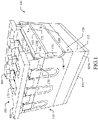
- the integrated device 100 comprises a MOS transistor 105 (or more).
- the MOS transistor 105 has a vertical structure of Split-Trench Gate (STG) type.
- STG Split-Trench Gate
- the MOS transistor 105 implements a power component, which is designed to handle relatively high electric power (for example, of the order of more than 10 W), such as operating at corresponding relatively high currents and/or voltages (for example, of the order of more than 10 A and 10 V, respectively).
- the MOS transistor 105 is integrated on a semiconductor bulk, such as a die 110 of semiconductor material, for example, silicon (so as to define a corresponding chip).
- concentrations of N-type and P-type dopants (or impurities) of the semiconductor material are denoted by adding the sign + or the sign - to the letters N and P to indicate a high or low concentration of impurities, respectively, or the sign ++ or the sign -- to indicate a very high or a very low concentration of impurities, respectively; the letters N and P without the addition of any sign + or - denote concentrations of intermediate value.
- the MOS transistor 105 comprises the following components.
- a drain region of N++ type is defined by the substrate 115 (extending into the die 110 from the back surface 125b).
- a body region 130 of P type extends into the epitaxial layer 120 from the front surface 125f, so as to remain separate from the drain region 115.
- the MOS transistor 105 has a cellular structure, with a same structure replicated throughout a plurality of cells (such as 100-1.000). Particularly, each cell comprises the following components.
- a source region 135 of N+ type extends into the body region 130 from the front surface 125f.
- a gate trench 140 extends into the body region 130 and then into the epitaxial layer 120 from the front surface 125f.
- the gate trench 140 is coated with (electrically) insulating material (for example, silicon oxide); particularly, a (relatively thin) gate insulating layer 145 coats an upper portion of the gate trench 140, from the front surface 120f substantially to the same depth of the body region 130, whereas a (relatively thick) separation insulating layer 150 coats a (remaining) lower portion of the gate trench 140.
- insulating material for example, silicon oxide
- the (coated) gate trench 140 is filled with (electrically) conductive material, such as doped polysilicon of N+ type, which is split into an upper portion defining a gate region 155 and a lower portion defining a field plate (or shield gate) 160 by a (relatively thick) splitting insulating layer 165 of (electrically) insulating material (for example, silicon oxide); the splitting insulating layer 165 extends between the gate insulating layer 145 and the separation insulating layer 150, so that the gate region 155 is substantially at the same depth of the body region 130 in the die 110.
- (electrically) conductive material such as doped polysilicon of N+ type
- the MOS transistor 105 has an interdigitated architecture; particularly, in plant view (on the front surface 125f) the source regions 135 and the gate regions 155 have an elongated shape (strips) and are arranged parallel, alternated to each other (like fingers of crossed hands).
- a drain contact 170 of (electrically) conductive material (for example, metal) contacts the drain region 115.
- a protective layer 175 of (electrically) insulating material for example, silicon dioxide) covers the front surface 125f (partially cut away in the figure for the sake of clarity).
- a source contact 180 of (electrically) conductive material contacts all the source regions 135 and the body region 130 through the protective layer 175.
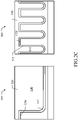
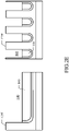
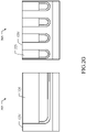
- FIG.2A-FIG.2M the main steps are shown of a manufacturing process of the integrated device according to an embodiment of the present disclosure.
- the figures are (partial) cross-section views across corresponding planes perpendicular of the front surface that extend in parallel (to the left) and transversally (to the right) with respect to longitudinal axes of the trench gates.
- the manufacturing process is performed at the level of a wafer 305 of semiconductor material, whereon the same structure is integrated simultaneously in a large number of identical areas thereof (only one referred to in the following for the sake of simplicity).
- the wafer 305 comprises a substrate of N++ type, which will form the substrate of the integrated devices and then is denoted with the same reference 115.
- An epitaxial layer of N type which will form the epitaxial layer of the integrated devices and then is denoted with the same reference 120, is grown thermally onto the substrate 115.
- a mask 310 for the gate trenches is formed onto a free main surface of the epitaxial layer 120, which will form the front surface of the integrated devices and then is denoted with the same reference 125f; for example, the mask 310 is obtained by growing a (relatively thick) layer of silicon oxide with a thermal oxidation step and then etching it through a photo-resist layer suitably patterned with photo-lithographic techniques (then stripped). The wafer 305 is etched through the mask 310 (for example, with a dry etching step) to form the gate trenches 140.
- a layer of silicon oxide 315 is formed onto the wafer 305, i.e., the front surface 125f and an exposed surface of the gate trenches 140 (for example, with a mixture of a thermal oxidation step and a deposition step); the layer of silicon oxide 315 is relatively thick (for example, with a thickness of 100-200 nm).
- a layer of doped polysilicon 320 of N+ type is deposited onto the wafer 305, i.e ., the layer of silicon oxide 315, so as to fill the (coated) gate trenches 140 and to cover the (coated) front surface 125f.
- the layer of doped polysilicon is etched (for example, with a dry etching step) to recess into the gate trench 140, down to remain only in a lower portion thereof; the remaining layer of doped polysilicon then forms the field plates 160 (with a desired thickness, depending on the voltage to be sustained by the MOS transistor).
- the layer of silicon oxide is etched selectively (for example, with a dry etching step); particularly, the etching only applies to an exposed portion of the layer of silicon oxide (i.e., on the front surface 125f and on a lateral surface of the upper portion of the gate trenches 140) so as to remove it. A remaining portion of the layer of silicon oxide (protected by the field plates 160) then defines the corresponding separation insulating layers 150.
- a layer of silicon oxide 325 is deposited onto the wafer 305, so as to fill the gate trenches 140 and to cover the front surface 125f.
- the wafer 305 is planarized (for example, with a Chemical Mechanical Polishing, CMP, step) to remove an excess of the layer of silicon oxide 325 on the front surface 125f.
- CMP Chemical Mechanical Polishing
- the layer of silicon oxide 325 is etched (for example, with a dry etching step) to recess into the gate trenches 140, down to remain only in corresponding portions at a bottom thereof with a relatively high thickness (for example, 100-200 nm).
- another layer of silicon oxide 330 is grown onto the wafer 305, i.e ., the front surface 125f, the lateral surface of the upper portions of the gate trenches 140 and the portions of the layer of silicon oxide 325 (for example, with a thermal oxidation step).
- corresponding portions of the layer of silicon oxide 330 that coat the upper portions of the gate trenches 140 defines the corresponding gate insulating layers 145
- corresponding portions of the layer of silicon oxide 330 that add to the portions of the layer of silicon oxide 325 in the gate trenches 140 (slightly increasing their thickness) define the corresponding splitting insulating layers 165.
- the layer of silicon oxide 330 has a relatively low thickness (for example, 30-50 nm), in any case far lower than the thickness of the splitting insulating layers 165 (130-250 nm in the example at issue).
- a (sacrificial) layer of a material different from the one of the layer of silicon oxide 330 is formed onto the wafer 305, i.e ., the layer of silicon oxide 330 both where alone and when contributing to form the splitting insulating layers 165.
- a layer of an auxiliary (electrically) insulating material such as a layer of silicon nitride (Si 3 N 4 ) 335 is deposited.
- the layer of silicon nitride 335 has a (relatively) low thickness (for example, 70-100 nm).
- a total thickness of a passing insulating layer formed by the superimposed layer of silicon oxide 330 (alone) and layer of silicon nitride 335 is (possibly strictly) lower than an implantation threshold ensuring that the passing insulating layer 330,335 does not substantially stop any implantation of dopants through it; conversely, a total thickness of a blocking insulating layer formed by the superimposed splitting insulating layers 165 and layer of silicon nitride 335 is higher than the implantation threshold, so as to ensure that the blocking insulating layer 165,335 substantially stops any implantation of dopants through it.
- the implantation threshold is 150-250 nm, preferably 180-220 nm and still more preferably 190-210 nm, such as 200 nm; the thickness of the passing insulating layer 330,335 is 0.4-0.9, preferably 0.5-0.8 and still more preferably 0.6-0.7, such as 0.65 times the implantation threshold, whereas the thickness of the blocking insulating layer 165,335 is 1.3-2.5, preferably 1.4-2.0 and still more preferably 1.5-1.8, such as 1.7 times the implantation threshold.
- two (ionic) implantation steps of dopants of P-type are performed in succession in the area of the trench gates 140 (with the rest of the wafer 305 suitably masked). In both cases, the dopants are shot into the wafer 305 along corresponding implantation directions that are tilted (not perpendicular) with respect to the front surface 125f.
- P-type for example, boron
- the implantation directions are symmetric to a normal to the front surface 125f; for example, the implantation directions form opposite angles with the normal equal to ⁇ 45°-60°, preferably ⁇ 47-58°, and still more preferably ⁇ 49-56°, such as ⁇ 51-54°.
- the dopants only cross the (thinner) superimposed layer of silicon oxide 330 and layer of silicon nitride 335, whereas they are blocked by the (thicker) superimposed splitting insulating layers 165 and layer of silicon nitride 335.
- corresponding regions of boron 340 are implanted below the front surface 125f and the lateral surface of the upper portions of the gate tranches 140 (and then aligned in depth with the layer of silicon nitride 335).
- an etching step is performed being selective to act on the material of the layer of silicon nitride but not on the material of the layer of silicon oxide 330 (for example, based on phosphoric acid).
- the layer of silicon nitride is removed without affecting the layer of silicon oxide 330 (and then the thickness of the gate insulating layers 145 and of the splitting insulating layers 165).
- a (further) layer of doped polysilicon 345 of N+ type is deposited onto the wafer 305, i.e ., the portion of the layer of silicon oxide 330 on the front surface 125f, the gate insulating layers 145 and the splitting insulating layers 165, so as to fill the (coated) upper portion of the gate trenches 140 and to cover the (coated) front surface 125f.
- the layer of doped polysilicon 345 is aligned in depth with the regions of boron 340 (apart from the thickness of the layer of silicon nitride that has been removed).
- the wafer 305 is planarized (for example, with a Chemical Mechanical Polishing, CMP, step) to remove an excess of the layer of doped polysilicon on the front surface 125f, thereby leaving the gate regions 155.
- the regions of boron are now diffused so as to obtain the body region 130.
- the gate regions 155 are substantially self-aligned in-depth with the body region 130 (apart from the thickness of the layer of silicon nitride that has been removed).
- the source regions 135 are formed with an (ionic) implantation step of dopants of N type (for example, arsenic) through a photo-resist mask (then stripped), followed by a thermal diffusion step.
- a relatively thick layer of silicon oxide is grown with a thermal oxidation step onto the wafer to form the protective layer 175.
- Corresponding windows for the source contact 180, the gate contact 185 and the contact of the field plates 160 are opened in the protective layer 175 by etching it through a photo-resist mask, then stripped.
- a layer of metal for example, tungsten is deposited onto the wafer, so as to fill the windows and to cover the (coated) front surface 125f, and it is then planarized (for example, with a CMP step) to remove an excess of the metal on the protective layer 175.
- a further layer of metal for example, copper is deposited onto the wafer and it is then etched through a photo-resist mask, then stripped, so as to define the source contact 180, the gate contact 185 and the contact of the field plates 160.
- a layer of metal for example, copper is deposited onto the back surface 125b of the wafer to form the drain contact 170.
- the integrated device 100 so obtained may be recognized because of peculiar features thereof being due to the tilted implantation steps.
- the body region 130 has a bottom surface within the die 110 with a concavity between each pair of adjacent trench gates 140, i.e., curved inwards it (towards the front surface 125f); for example, a distance between its deepest point in the die 110 (close to the trench gates 140) and its shallowest point in the die 110 (in the middle between the trench gates 140) is about 2-10% of a thickness of the body region 130.
- the integrated device 100 may be recognized by analyzing it with a Secondary-Ion Mass Spectrometry (SIMS) technique; indeed, in this way it is possible to point out the typical dopant profile due to the implantation process (i.e ., with its concentration increasing towards a maximum value and then decreeing) moving obliquely inwards the die 110 from the front surface 125f and the lateral surface of the (upper portions) of the trench gates 140.
- SIMS Secondary-Ion Mass Spectrometry
- FIG.3 a schematic block diagram is shown of a system 300 incorporating the integrated device according to an embodiment of the present disclosure.
- the system 300 (for example, a control unit for automotive applications) comprises several components that are connected among them through a bus structure 305 (with one or more levels). Particularly, one or more microprocessors ( ⁇ P) 310 provide a logic capability of the system 300; a non-volatile memory (ROM) 315 stores basic code for a bootstrap of the system 300 and a volatile memory (RAM) 320 is used as a working memory by the microprocessors 310.
- the system has a mass-memory 325 for storing programs and data (for example, a flash E 2 PROM).
- the system 300 comprises a number of controllers of peripheral, or Input/Output (I/O), units, 330 (such as a Wi-Fi WNIC, a Bluetooth transceiver, a GPS receiver, an accelerometer, a gyroscope and so on).
- I/O Input/Output
- the peripherals 330 each comprises the integrated device 100.
- an embodiment provides a process for manufacturing an integrated device.
- the integrated device may be manufactured with any technologies, with masks being different in number and in type, or with other process steps/parameters.
- the above-described solution may be part of the design of an integrated device.
- the design may also be created in a hardware description language; moreover, if the designer does not manufacture chips or masks, the design may be transmitted by physical means to others.
- the integrated device comprises at least one MOS transistor integrated on a die of semiconductor material of a first type of conductivity having a main surface.
- the integrated device may be of any type (see below) and integrated on a die of any type (for example, an epitaxial layer grown on a substrate, a monocrystalline substrate, a SOI and so on) and of any semiconductor material (for example, silicon, germanium, with any type and concentration of dopants, and so on).
- the process comprises forming one or more gate trenches extending from the main surface into the die.
- the gate trenches may be in any number and of any shape, size and depth (for example, with a U section in a UMOS, a V section in a VMOS and so on).
- the process comprises coating the gate trenches with an electrically insulating material to obtain corresponding coated internal (or lower) portions of the gate trenches (being coated with corresponding separation insulating layers) and corresponding coated external (or upper) portions of the gate trenches (being coated with corresponding gate insulating layers).
- the internal/external portions of the gate trenches may have any depth (in either relative or absolute terms); moreover, the separation/gate insulation layers may be of any material (either the same or different to each other, such as silicon oxide, silicon nitride, TEOS and so on), any thickness (in either relative or absolute terms) and they may formed in any way (for example, with one or more growing steps and/or deposition steps, either selective or not, with possible etching steps and so on).
- the process comprises filling the coated inner (or lower) portions of the gate trenches with electrically conductive material forming corresponding field plates.
- the field plates may be of any material (for example, polysilicon, metal and so on) and they may be formed in any way (for example, with deposition, planarization and etching steps, deposition and etching steps, selective deposition step and so on).
- the process comprises covering the field plates with corresponding splitting insulating layers of electrically insulating material.
- the splitting insulating layers may be of any material (either the same or different with respect to the separation/gate insulating layers), any thickness (either the same or different with respect to the separation insulating layer) and they may be formed in any way (for example, with a deposition step, a growing step, either selective or followed by an etching step, and so on).
- the process comprises implanting dopants of a second type of conductivity into the die from the main surface.
- the dopants may be of any type (for example, boron, arsenic and so on) and they may be implanted in any way (for example, with any energy, length and so on).
- the dopants are implanted along one or more implantation directions being tilted with respect to the front surface.
- the dopants may be implanted along any number of implantation directions forming any non-null angle with the front surface.
- the dopants are implanted selectively by passing in an implantation zone (at the front surface and a lateral surface of the external portions of the gate trenches) and being blocked in a blocking zone (at the splitting insulating layers).
- this selective implantation may be obtained in any way (for example, with insulating layers of different thickness, a mask and so on).
- the process comprises diffusing the dopants being implanted to form a body region.
- the dopants may be diffused in any way (for example, with any temperature, length and so on).
- the process comprises filling the coated external portions of the gate trenches with electrically conductive material forming corresponding gate regions (thereby being substantially self-aligned in depth from the main surface with the body region).
- the gate regions may be of any material (for example, either the same or different with respect to the field plates) and they may be formed in any way (for example, with deposition and planarization steps, selective deposition step and so on); moreover, the gate regions and the body region may be self-aligned with any tolerance (for example, up to 10%, preferably 5% and still more preferably 3%, such as 2% of the depth of the body region).
- the process comprises implanting the dopants along a first one and a second one of the implantation directions forming a first angle and a second angle, respectively, with a normal to the front surface having opposite values.
- the possibility is not excluded of using more implantation directions, even not symmetric (for example, with the addition of an implantation direction perpendicular to the front surface).
- the first angle and the second angle are ⁇ 51-54°. However, different angles are contemplated.
- the process comprises implanting the dopants selectively by passing through a passing insulating layer of electrically insulating material at the passing zone and being blocked by a blocking insulating layer of electrically insulating material at the blocking zone having a thickness being lower and higher, respectively, than an implantation threshold.
- the passing/blocking insulating layers may be formed in any way (for example, via a sacrificial insulating layer, directly and so on) and they may have any thickness (in either absolute or relative terms).
- the process comprises forming an auxiliary insulating layer of electrically insulating material on the implantation zone over the gate insulating layers and on the blocking zone over the splitting insulating layers to obtain the passing insulating layer and the blocking insulating layer, respectively.
- the auxiliary insulating layer may be of any type (for example, of any material, thickness and so on) and it may be formed in any way (for example, deposited, grown and so on).
- the process comprises removing the auxiliary insulating layer after said implanting the dopants.
- the auxiliary insulating layer may be removed in any way (for example, with a wet etching step, a dry etching step and so on), down to none.
- the electrically insulating material of the auxiliary insulating layer is different from the electrically insulating material of the gate insulating layers and of the splitting insulating layers.
- the materials may be of any type (even the same, at least in part).
- the process comprises removing the auxiliary insulating layer after said implanting the dopants by a selective etching acting on the electrically insulating material of the auxiliary insulating layer and not acting on the electrically insulating material of the gate insulating layers and of the splitting insulating layers.
- the selective etching may be performed in any way (for example, with any selective solutions) or in a different way (for example, via a corresponding mask).
- the electrically insulating material of the auxiliary insulating layer is silicon nitride and the electrically insulating material of the gate insulating layers and of the splitting insulating layers is silicon oxide.
- the use of different materials is contemplated.
- An embodiment provides an integrated device comprising at least one MOS transistor integrated on a die of semiconductor material.
- the integrated device may be of any type (for example, in raw wafer form, as a bare die, in a package, and so on) and comprising any number and type of MOS transistors (for example, NMOS, PMOS, of power/signal/mixed type, with a cellular/simple structure and so on).
- the integrated device is manufactured by the above-mentioned process.
- the integrated device may be recognized by any number and type of corresponding peculiar features (for example, the concavities of the body region, its dopant profile and so on).
- An embodiment provides a system comprising at least one integrated device as above.
- the same structure may be integrated with other circuits in the same chip; the chip may also be coupled with one or more other chips, it may be mounted in intermediate products or it may be used in complex apparatus.
- the resulting system may be of any type (for example, for use in automotive applications, smartphones, computers and so on) and it may comprise any number of these integrated devices.
- any interaction between different components generally does not need to be continuous, and it may be either direct or indirect through one or more intermediaries.
Landscapes
- Electrodes Of Semiconductors (AREA)
- Insulated Gate Type Field-Effect Transistor (AREA)
- Metal-Oxide And Bipolar Metal-Oxide Semiconductor Integrated Circuits (AREA)
- Chemical & Material Sciences (AREA)
- Crystallography & Structural Chemistry (AREA)
Abstract
Description
- The present disclosure relates to the field of integrated devices. More specifically, this disclosure relates to MOS transistors.
- The background of the present disclosure is hereinafter introduced with the discussion of techniques relating to its context. However, even when this discussion refers to documents, acts, artifacts and the like, it does not suggest or represent that the discussed techniques are part of the prior art or are common general knowledge in the field relevant to the present disclosure.
- Integrated devices based on MOS transistors are commonly used in several applications. Particularly, the MOS transistors are among the most common components in power applications, wherein substantial amounts of electrical energy are processed; in this case, the MOS transistors are designed to operate at relatively high voltages and/or currents.
- The (power) MOS transistors generally have a cellular structure. Each MOS transistor replicates a same structure throughout several cells that are formed in a same die of semiconductor material whereon the MOS transistor is integrated; the cells comprise corresponding (basic) gate regions and source regions that are connected in parallel, for example, in the form of alternated strips (providing a high ratio perimeter/area of the source regions). Moreover, the MOS transistors generally have a vertical structure. Each MOS transistor has its source regions at a front surface of the die and a (common) drain region at a back surface of the die, opposite to each other; in this way, a channel that forms in operation between the source regions and the drain region extends across the die. All of the above allows the MOS transistor to sustain both high currents (thanks its wide channel) and high voltages (thanks to its long channel) in a relatively small area of the die.
- Particularly, in MOS transistors of trench-gate type the gate regions are formed in corresponding trenches extending from the front surface of the die; each trench is coated with a (relatively thin) insulating layer, and it is then filled with conductive material (such as doped polysilicon) forming the gate region. In this way, the channels of the MOS transistor are formed along (vertical) walls of the trenches.
- The MOS transistors may also be provided with field plates. Each field plate comprises an (insulated) region of conductive material, arranged between a corresponding gate region and the drain region (close to the corresponding channel). In operation, the field plates are maintained at a reference voltage (or ground). The field plates reduce a gate/drain capacitance Cdg of the MOS transistor; this increases a switching frequency of the MOS transistor accordingly. Moreover, the field plates reduce a drain/source on-state, or output, resistance RDSon of the MOS transistor; this increases a Safe Operating Area (SOA) of the MOS transistor accordingly.
- Particularly, in MOS transistors of split-gate (or shielded-gate) type the field plates are formed by corresponding additional gate regions (shield gates) buried in their tranches. The field plates are arranged below the corresponding actual gate regions (upper gates), which control the formation of the corresponding channels of the MOS transistor in operation as usual.
- Therefore, a body region of the MOS transistor (wherein the source regions are formed) should be maintained at the same depth as the gate regions in the die as far as possible. For this purpose, after each trench has been coated with the insulating layer and filled with the doped polysilicon, the latter is etched to recess into the trench down to a level corresponding to the desired thickness of the field plate. Insulating material is then deposited over the whole die and then etched to form a (relatively thick) insulating layer in the trench, above the field plate. At this point, the trench is filled again with the doped polysilicon to form the gate region.
- However, a thickness of the corresponding insulating layers between the field plates and the gate regions is subject to a (relatively large) spread due to the etching performed for their formation. Therefore, the body region and the gate regions may be at different depth in the die. This misalignment (between the body region and the gate regions) generates corresponding variations (and increase) of the gate/drain capacitance Cdg of the MOS transistor. Moreover, the same misalignment significantly increases the drain/source on-state resistance RDSon of the MOS transistor. As a consequence, the increased gate/drain capacitance Cdg reduces the switching frequency and the increased on-state resistance RDSon reduces the SOA of the MOS transistor accordingly. All of the above adversely affects performance of the MOS transistor (partially undermining the advantages provided by the split-gate structure).
- Document
CN 108 511 515 relates to power semiconductor devices, and in particular relates to a new method for adjusting the channel length of a field effect transistor and a manufacturing process thereof. - Document
US 2007/082441 relates in general to semiconductor power device technology and in particular to trench gate field effect transistors with improved body to gate alignment. - A simplified summary of the present disclosure is herein presented in order to provide a basic understanding thereof; however, the sole purpose of this summary is to introduce some concepts of the disclosure in a simplified form as a prelude to its following more detailed description, and it is not to be interpreted as an identification of its key elements nor as a delineation of its scope.
- In general terms, the present disclosure is based on the idea of self-aligning the body region with the gate regions.
- Particularly, an aspect provides a process for manufacturing an integrated device, which comprises at least one MOS transistor integrated on a die of semiconductor material. The process comprises forming one or more gate trenches with corresponding field plates and gate regions; a body region is formed by implanting dopants selectively along one or more implantation directions that are tilted with respect to a front surface of the die.
- A further aspect provides a corresponding integrated device.
- A further aspect provides a system comprising at least one integrated device as above.
- More specifically, one or more aspects of the present disclosure are set out in the independent claims and advantageous features thereof are set out in the dependent claims, with the wording of all the claims that is herein incorporated verbatim by reference (with any advantageous feature provided with reference to any specific aspect that applies mutatis mutandis to every other aspect).
- The solution of the present disclosure, as well as further features and the advantages thereof, will be best understood with reference to the following detailed description thereof, given purely by way of a non-restrictive indication, to be read in conjunction with the accompanying drawings (wherein, for the sake of simplicity, corresponding elements are denoted with equal or similar references and their explanation is not repeated, and the name of each entity is generally used to denote both its type and its attributes, like value, content and representation). In this respect, it is expressly intended that the drawings are not necessary drawn to scale (with some details that may be exaggerated and/or simplified) and that, unless otherwise indicated, they are merely used to illustrate the structures and procedures described herein conceptually. Particularly:
-
FIG.1 shows a partial pictorial representation in cross-section view of an integrated device according to an embodiment of the present disclosure, -
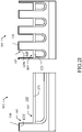
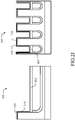
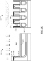
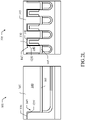
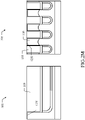
FIG.2A-FIG.2M show the main steps of a manufacturing process of the integrated device according to an embodiment of the present disclosure, and -
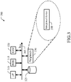
FIG.3 shown a schematic block diagram of a system incorporating the integrated device according to an embodiment of the present disclosure. - With reference in particular to
FIG.1 , a partial pictorial representation is shown in cross-section view of an integrateddevice 100 according to an embodiment of the present disclosure. - The
integrated device 100 comprises a MOS transistor 105 (or more). TheMOS transistor 105 has a vertical structure of Split-Trench Gate (STG) type. TheMOS transistor 105 implements a power component, which is designed to handle relatively high electric power (for example, of the order of more than 10 W), such as operating at corresponding relatively high currents and/or voltages (for example, of the order of more than 10 A and 10 V, respectively). - The
MOS transistor 105 is integrated on a semiconductor bulk, such as a die 110 of semiconductor material, for example, silicon (so as to define a corresponding chip). As usual, the concentrations of N-type and P-type dopants (or impurities) of the semiconductor material are denoted by adding the sign + or the sign - to the letters N and P to indicate a high or low concentration of impurities, respectively, or the sign ++ or the sign -- to indicate a very high or a very low concentration of impurities, respectively; the letters N and P without the addition of any sign + or - denote concentrations of intermediate value. The die 110 comprises asubstrate 115 of N++ type (far thicker in reality), over which a (thin)epitaxial layer 120 of N type is arranged. A free main surface of theepitaxial layer 120 defines afront surface 125f of thedie 110, whereas a free main surface of thesubstrate 115 defines aback surface 125b of the die 110 (opposite to each other). - The
MOS transistor 105 comprises the following components. A drain region of N++ type is defined by the substrate 115 (extending into the die 110 from theback surface 125b). Abody region 130 of P type extends into theepitaxial layer 120 from thefront surface 125f, so as to remain separate from thedrain region 115. TheMOS transistor 105 has a cellular structure, with a same structure replicated throughout a plurality of cells (such as 100-1.000). Particularly, each cell comprises the following components. Asource region 135 of N+ type extends into thebody region 130 from thefront surface 125f. Agate trench 140 extends into thebody region 130 and then into theepitaxial layer 120 from thefront surface 125f. Thegate trench 140 is coated with (electrically) insulating material (for example, silicon oxide); particularly, a (relatively thin)gate insulating layer 145 coats an upper portion of thegate trench 140, from the front surface 120f substantially to the same depth of thebody region 130, whereas a (relatively thick)separation insulating layer 150 coats a (remaining) lower portion of thegate trench 140. The (coated)gate trench 140 is filled with (electrically) conductive material, such as doped polysilicon of N+ type, which is split into an upper portion defining agate region 155 and a lower portion defining a field plate (or shield gate) 160 by a (relatively thick) splitting insulatinglayer 165 of (electrically) insulating material (for example, silicon oxide); the splitting insulatinglayer 165 extends between thegate insulating layer 145 and theseparation insulating layer 150, so that thegate region 155 is substantially at the same depth of thebody region 130 in thedie 110. - The
MOS transistor 105 has an interdigitated architecture; particularly, in plant view (on thefront surface 125f) thesource regions 135 and thegate regions 155 have an elongated shape (strips) and are arranged parallel, alternated to each other (like fingers of crossed hands). Adrain contact 170 of (electrically) conductive material (for example, metal) contacts thedrain region 115. Aprotective layer 175 of (electrically) insulating material (for example, silicon dioxide) covers thefront surface 125f (partially cut away in the figure for the sake of clarity). Asource contact 180 of (electrically) conductive material (for example, metal) contacts all thesource regions 135 and thebody region 130 through theprotective layer 175. Agate contact 185 of (electrically) conductive material (for example, metal) contacts all thegate regions 155 through theprotective layer 175. A further contact (not shown in the figure) contacts all the field plates 160 (in a portion of thegate trenches 140 without thegate regions 155 and the splitting insulatinglayers 165, where thefield plates 160 extend up to thefront surface 125f). - With reference now to
FIG.2A-FIG.2M , the main steps are shown of a manufacturing process of the integrated device according to an embodiment of the present disclosure. - Particularly, the figures are (partial) cross-section views across corresponding planes perpendicular of the front surface that extend in parallel (to the left) and transversally (to the right) with respect to longitudinal axes of the trench gates.
- Starting from
FIG.2A , as usual the manufacturing process is performed at the level of awafer 305 of semiconductor material, whereon the same structure is integrated simultaneously in a large number of identical areas thereof (only one referred to in the following for the sake of simplicity). Thewafer 305 comprises a substrate of N++ type, which will form the substrate of the integrated devices and then is denoted with thesame reference 115. An epitaxial layer of N type, which will form the epitaxial layer of the integrated devices and then is denoted with thesame reference 120, is grown thermally onto thesubstrate 115. Amask 310 for the gate trenches is formed onto a free main surface of theepitaxial layer 120, which will form the front surface of the integrated devices and then is denoted with thesame reference 125f; for example, themask 310 is obtained by growing a (relatively thick) layer of silicon oxide with a thermal oxidation step and then etching it through a photo-resist layer suitably patterned with photo-lithographic techniques (then stripped). Thewafer 305 is etched through the mask 310 (for example, with a dry etching step) to form thegate trenches 140. - Moving to
FIG.2B , the mask is removed. A layer ofsilicon oxide 315 is formed onto thewafer 305, i.e., thefront surface 125f and an exposed surface of the gate trenches 140 (for example, with a mixture of a thermal oxidation step and a deposition step); the layer ofsilicon oxide 315 is relatively thick (for example, with a thickness of 100-200 nm). - Moving to
FIG.2C , a layer of dopedpolysilicon 320 of N+ type is deposited onto thewafer 305, i.e., the layer ofsilicon oxide 315, so as to fill the (coated)gate trenches 140 and to cover the (coated)front surface 125f. - Moving to
FIG.2D , the layer of doped polysilicon is etched (for example, with a dry etching step) to recess into thegate trench 140, down to remain only in a lower portion thereof; the remaining layer of doped polysilicon then forms the field plates 160 (with a desired thickness, depending on the voltage to be sustained by the MOS transistor). - Moving to
FIG.2E , the layer of silicon oxide is etched selectively (for example, with a dry etching step); particularly, the etching only applies to an exposed portion of the layer of silicon oxide (i.e., on thefront surface 125f and on a lateral surface of the upper portion of the gate trenches 140) so as to remove it. A remaining portion of the layer of silicon oxide (protected by the field plates 160) then defines the correspondingseparation insulating layers 150. - Moving to
FIG.2F , a layer ofsilicon oxide 325 is deposited onto thewafer 305, so as to fill thegate trenches 140 and to cover thefront surface 125f. - Moving to
FIG.2G , thewafer 305 is planarized (for example, with a Chemical Mechanical Polishing, CMP, step) to remove an excess of the layer ofsilicon oxide 325 on thefront surface 125f. - Moving to
FIG.2H , the layer ofsilicon oxide 325 is etched (for example, with a dry etching step) to recess into thegate trenches 140, down to remain only in corresponding portions at a bottom thereof with a relatively high thickness (for example, 100-200 nm). - Moving to
FIG.2I , another layer ofsilicon oxide 330 is grown onto thewafer 305, i.e., thefront surface 125f, the lateral surface of the upper portions of thegate trenches 140 and the portions of the layer of silicon oxide 325 (for example, with a thermal oxidation step). Particularly, corresponding portions of the layer ofsilicon oxide 330 that coat the upper portions of thegate trenches 140 defines the correspondinggate insulating layers 145, whereas corresponding portions of the layer ofsilicon oxide 330 that add to the portions of the layer ofsilicon oxide 325 in the gate trenches 140 (slightly increasing their thickness) define the corresponding splitting insulatinglayers 165. The layer ofsilicon oxide 330 has a relatively low thickness (for example, 30-50 nm), in any case far lower than the thickness of the splitting insulating layers 165 (130-250 nm in the example at issue). - Moving to
FIG.2J , in the solution according to an embodiment of the present disclosure, a (sacrificial) layer of a material different from the one of the layer ofsilicon oxide 330 is formed onto thewafer 305, i.e., the layer ofsilicon oxide 330 both where alone and when contributing to form the splitting insulatinglayers 165. For example, a layer of an auxiliary (electrically) insulating material, such as a layer of silicon nitride (Si3N4) 335 is deposited. The layer ofsilicon nitride 335 has a (relatively) low thickness (for example, 70-100 nm). Particularly, a total thickness of a passing insulating layer formed by the superimposed layer of silicon oxide 330 (alone) and layer ofsilicon nitride 335 is (possibly strictly) lower than an implantation threshold ensuring that the passing insulating layer 330,335 does not substantially stop any implantation of dopants through it; conversely, a total thickness of a blocking insulating layer formed by the superimposed splitting insulatinglayers 165 and layer ofsilicon nitride 335 is higher than the implantation threshold, so as to ensure that the blocking insulating layer 165,335 substantially stops any implantation of dopants through it. For example, the implantation threshold is 150-250 nm, preferably 180-220 nm and still more preferably 190-210 nm, such as 200 nm; the thickness of the passing insulating layer 330,335 is 0.4-0.9, preferably 0.5-0.8 and still more preferably 0.6-0.7, such as 0.65 times the implantation threshold, whereas the thickness of the blocking insulating layer 165,335 is 1.3-2.5, preferably 1.4-2.0 and still more preferably 1.5-1.8, such as 1.7 times the implantation threshold. - Moving to
FIG.2K , two (ionic) implantation steps of dopants of P-type (for example, boron) are performed in succession in the area of the trench gates 140 (with the rest of thewafer 305 suitably masked). In both cases, the dopants are shot into thewafer 305 along corresponding implantation directions that are tilted (not perpendicular) with respect to thefront surface 125f. Particularly, in any plane perpendicular to thefront surface 125f and to the axes of the trench gates 140 (to the right in the figure) the implantation directions are symmetric to a normal to thefront surface 125f; for example, the implantation directions form opposite angles with the normal equal to ±45°-60°, preferably ±47-58°, and still more preferably ±49-56°, such as ±51-54°. In view of the above, the dopants only cross the (thinner) superimposed layer ofsilicon oxide 330 and layer ofsilicon nitride 335, whereas they are blocked by the (thicker) superimposed splitting insulatinglayers 165 and layer ofsilicon nitride 335. As a consequence, corresponding regions ofboron 340 are implanted below thefront surface 125f and the lateral surface of the upper portions of the gate tranches 140 (and then aligned in depth with the layer of silicon nitride 335). - Moving to
FIG.2L , an etching step is performed being selective to act on the material of the layer of silicon nitride but not on the material of the layer of silicon oxide 330 (for example, based on phosphoric acid). As a result, the layer of silicon nitride is removed without affecting the layer of silicon oxide 330 (and then the thickness of thegate insulating layers 145 and of the splitting insulating layers 165). A (further) layer of dopedpolysilicon 345 of N+ type is deposited onto thewafer 305, i.e., the portion of the layer ofsilicon oxide 330 on thefront surface 125f, thegate insulating layers 145 and the splitting insulatinglayers 165, so as to fill the (coated) upper portion of thegate trenches 140 and to cover the (coated)front surface 125f. In view of the above, the layer of dopedpolysilicon 345 is aligned in depth with the regions of boron 340 (apart from the thickness of the layer of silicon nitride that has been removed). - Moving to
FIG.2M , thewafer 305 is planarized (for example, with a Chemical Mechanical Polishing, CMP, step) to remove an excess of the layer of doped polysilicon on thefront surface 125f, thereby leaving thegate regions 155. The regions of boron are now diffused so as to obtain thebody region 130. In view of the above, thegate regions 155 are substantially self-aligned in-depth with the body region 130 (apart from the thickness of the layer of silicon nitride that has been removed). - The process then continues as usual to obtain the
integrated device 100 shown inFIG.1 . Particularly, thesource regions 135 are formed with an (ionic) implantation step of dopants of N type (for example, arsenic) through a photo-resist mask (then stripped), followed by a thermal diffusion step. A relatively thick layer of silicon oxide is grown with a thermal oxidation step onto the wafer to form theprotective layer 175. Corresponding windows for thesource contact 180, thegate contact 185 and the contact of the field plates 160 (not shown in the figure) are opened in theprotective layer 175 by etching it through a photo-resist mask, then stripped. A layer of metal (for example, tungsten) is deposited onto the wafer, so as to fill the windows and to cover the (coated)front surface 125f, and it is then planarized (for example, with a CMP step) to remove an excess of the metal on theprotective layer 175. A further layer of metal (for example, copper) is deposited onto the wafer and it is then etched through a photo-resist mask, then stripped, so as to define thesource contact 180, thegate contact 185 and the contact of thefield plates 160. A layer of metal (for example, copper) is deposited onto theback surface 125b of the wafer to form thedrain contact 170. - The
integrated device 100 so obtained (with thegate regions 155 self-aligned in depth with the body region 130) may be recognized because of peculiar features thereof being due to the tilted implantation steps. Indeed, in this case thebody region 130 has a bottom surface within thedie 110 with a concavity between each pair ofadjacent trench gates 140, i.e., curved inwards it (towards thefront surface 125f); for example, a distance between its deepest point in the die 110 (close to the trench gates 140) and its shallowest point in the die 110 (in the middle between the trench gates 140) is about 2-10% of a thickness of thebody region 130. In addition or in alternative, theintegrated device 100 may be recognized by analyzing it with a Secondary-Ion Mass Spectrometry (SIMS) technique; indeed, in this way it is possible to point out the typical dopant profile due to the implantation process (i.e., with its concentration increasing towards a maximum value and then decreeing) moving obliquely inwards the die 110 from thefront surface 125f and the lateral surface of the (upper portions) of thetrench gates 140. - With reference now to
FIG.3 , a schematic block diagram is shown of asystem 300 incorporating the integrated device according to an embodiment of the present disclosure. - The system 300 (for example, a control unit for automotive applications) comprises several components that are connected among them through a bus structure 305 (with one or more levels). Particularly, one or more microprocessors (µP) 310 provide a logic capability of the
system 300; a non-volatile memory (ROM) 315 stores basic code for a bootstrap of thesystem 300 and a volatile memory (RAM) 320 is used as a working memory by themicroprocessors 310. The system has a mass-memory 325 for storing programs and data (for example, a flash E2PROM). Moreover, thesystem 300 comprises a number of controllers of peripheral, or Input/Output (I/O), units, 330 (such as a Wi-Fi WNIC, a Bluetooth transceiver, a GPS receiver, an accelerometer, a gyroscope and so on). Particularly, one or more of theperipherals 330 each comprises theintegrated device 100. - Naturally, in order to satisfy local and specific requirements, a person skilled in the art may apply many logical and/or physical modifications and alterations to the present disclosure. More specifically, although this disclosure has been described with a certain degree of particularity with reference to one or more embodiments thereof, it should be understood that various omissions, substitutions and changes in the form and details as well as other embodiments are possible. Particularly, different embodiments of the present disclosure may even be practiced without the specific details (such as the numerical values) set forth in the preceding description to provide a more thorough understanding thereof; conversely, well-known features may have been omitted or simplified in order not to obscure the description with unnecessary particulars. Moreover, it is expressly intended that specific elements and/or method steps described in connection with any embodiment of the present disclosure may be incorporated in any other embodiment as a matter of general design choice. Moreover, items presented in a same group and different embodiments, examples or alternatives are not to be construed as de facto equivalent to each other (but they are separate and autonomous entities). In any case, each numerical value should be read as modified according to applicable tolerances; particularly, unless otherwise indicated, the terms "substantially", "about", "approximately" and the like should be understood as within 10%, preferably 5% and still more preferably 1%. Moreover, each range of numerical values should be intended as expressly specifying any possible number along the continuum within the range (comprising its end points). Ordinal or other qualifiers are merely used as labels to distinguish elements with the same name but do not by themselves connote any priority, precedence or order. The terms include, comprise, have, contain, involve and the like should be intended with an open, non-exhaustive meaning (i.e., not limited to the recited items), the terms based on, dependent on, according to, function of and the like should be intended as a non-exclusive relationship (i.e., with possible further variables involved), the term a/an should be intended as one or more items (unless expressly indicated otherwise), and the term means for (or any means-plus-function formulation) should be intended as any structure adapted or configured for carrying out the relevant function.
- For example, an embodiment provides a process for manufacturing an integrated device. However, the integrated device may be manufactured with any technologies, with masks being different in number and in type, or with other process steps/parameters. Moreover, the above-described solution may be part of the design of an integrated device. The design may also be created in a hardware description language; moreover, if the designer does not manufacture chips or masks, the design may be transmitted by physical means to others.
- In an embodiment, the integrated device comprises at least one MOS transistor integrated on a die of semiconductor material of a first type of conductivity having a main surface. However, the integrated device may be of any type (see below) and integrated on a die of any type (for example, an epitaxial layer grown on a substrate, a monocrystalline substrate, a SOI and so on) and of any semiconductor material (for example, silicon, germanium, with any type and concentration of dopants, and so on).
- In an embodiment, the process comprises forming one or more gate trenches extending from the main surface into the die. However, the gate trenches may be in any number and of any shape, size and depth (for example, with a U section in a UMOS, a V section in a VMOS and so on).
- In an embodiment, the process comprises coating the gate trenches with an electrically insulating material to obtain corresponding coated internal (or lower) portions of the gate trenches (being coated with corresponding separation insulating layers) and corresponding coated external (or upper) portions of the gate trenches (being coated with corresponding gate insulating layers). However, the internal/external portions of the gate trenches may have any depth (in either relative or absolute terms); moreover, the separation/gate insulation layers may be of any material (either the same or different to each other, such as silicon oxide, silicon nitride, TEOS and so on), any thickness (in either relative or absolute terms) and they may formed in any way (for example, with one or more growing steps and/or deposition steps, either selective or not, with possible etching steps and so on).
- In an embodiment, the process comprises filling the coated inner (or lower) portions of the gate trenches with electrically conductive material forming corresponding field plates. However, the field plates may be of any material (for example, polysilicon, metal and so on) and they may be formed in any way (for example, with deposition, planarization and etching steps, deposition and etching steps, selective deposition step and so on).
- In an embodiment, the process comprises covering the field plates with corresponding splitting insulating layers of electrically insulating material. However, the splitting insulating layers may be of any material (either the same or different with respect to the separation/gate insulating layers), any thickness (either the same or different with respect to the separation insulating layer) and they may be formed in any way (for example, with a deposition step, a growing step, either selective or followed by an etching step, and so on).
- In an embodiment, the process comprises implanting dopants of a second type of conductivity into the die from the main surface. However, the dopants may be of any type (for example, boron, arsenic and so on) and they may be implanted in any way (for example, with any energy, length and so on).
- In an embodiment, the dopants are implanted along one or more implantation directions being tilted with respect to the front surface. However, the dopants may be implanted along any number of implantation directions forming any non-null angle with the front surface.
- In an embodiment, the dopants are implanted selectively by passing in an implantation zone (at the front surface and a lateral surface of the external portions of the gate trenches) and being blocked in a blocking zone (at the splitting insulating layers). However, this selective implantation may be obtained in any way (for example, with insulating layers of different thickness, a mask and so on).
- In an embodiment, the process comprises diffusing the dopants being implanted to form a body region. However, the dopants may be diffused in any way (for example, with any temperature, length and so on).
- In an embodiment, the process comprises filling the coated external portions of the gate trenches with electrically conductive material forming corresponding gate regions (thereby being substantially self-aligned in depth from the main surface with the body region). However, the gate regions may be of any material (for example, either the same or different with respect to the field plates) and they may be formed in any way (for example, with deposition and planarization steps, selective deposition step and so on); moreover, the gate regions and the body region may be self-aligned with any tolerance (for example, up to 10%, preferably 5% and still more preferably 3%, such as 2% of the depth of the body region).
- Further embodiments provide additional advantageous features, which may however be omitted at all in a basic implementation.
- Particularly, in an embodiment the process comprises implanting the dopants along a first one and a second one of the implantation directions forming a first angle and a second angle, respectively, with a normal to the front surface having opposite values. However, the possibility is not excluded of using more implantation directions, even not symmetric (for example, with the addition of an implantation direction perpendicular to the front surface).
- In an embodiment, the first angle and the second angle are ±51-54°. However, different angles are contemplated.
- In an embodiment, the process comprises implanting the dopants selectively by passing through a passing insulating layer of electrically insulating material at the passing zone and being blocked by a blocking insulating layer of electrically insulating material at the blocking zone having a thickness being lower and higher, respectively, than an implantation threshold. However, the passing/blocking insulating layers may be formed in any way (for example, via a sacrificial insulating layer, directly and so on) and they may have any thickness (in either absolute or relative terms).
- In an embodiment, the implantation threshold is 200 nm. However, different values of the implantation threshold are contemplated (for example, varying according to the energy, the length and so on of the implantation steps).
- In an embodiment, the process comprises forming an auxiliary insulating layer of electrically insulating material on the implantation zone over the gate insulating layers and on the blocking zone over the splitting insulating layers to obtain the passing insulating layer and the blocking insulating layer, respectively. However, the auxiliary insulating layer may be of any type (for example, of any material, thickness and so on) and it may be formed in any way (for example, deposited, grown and so on).
- In an embodiment, the process comprises removing the auxiliary insulating layer after said implanting the dopants. However, the auxiliary insulating layer may be removed in any way (for example, with a wet etching step, a dry etching step and so on), down to none.
- In an embodiment, the electrically insulating material of the auxiliary insulating layer is different from the electrically insulating material of the gate insulating layers and of the splitting insulating layers. However, the materials may be of any type (even the same, at least in part).
- In an embodiment, the process comprises removing the auxiliary insulating layer after said implanting the dopants by a selective etching acting on the electrically insulating material of the auxiliary insulating layer and not acting on the electrically insulating material of the gate insulating layers and of the splitting insulating layers. However, the selective etching may be performed in any way (for example, with any selective solutions) or in a different way (for example, via a corresponding mask).
- In an embodiment, the electrically insulating material of the auxiliary insulating layer is silicon nitride and the electrically insulating material of the gate insulating layers and of the splitting insulating layers is silicon oxide. However, the use of different materials is contemplated.
- Generally, similar considerations apply if the same solution is implemented with an equivalent method (by using similar steps with the same functions of more steps or portions thereof, removing some non-essential steps or adding further optional steps); moreover, the steps may be performed in a different order, concurrently or in an interleaved way (at least in part).
- An embodiment provides an integrated device comprising at least one MOS transistor integrated on a die of semiconductor material. However, the integrated device may be of any type (for example, in raw wafer form, as a bare die, in a package, and so on) and comprising any number and type of MOS transistors (for example, NMOS, PMOS, of power/signal/mixed type, with a cellular/simple structure and so on).
- In an embodiment, the integrated device is manufactured by the above-mentioned process. However, the integrated device may be recognized by any number and type of corresponding peculiar features (for example, the concavities of the body region, its dopant profile and so on).
- An embodiment provides a system comprising at least one integrated device as above. However, the same structure may be integrated with other circuits in the same chip; the chip may also be coupled with one or more other chips, it may be mounted in intermediate products or it may be used in complex apparatus. In any case, the resulting system may be of any type (for example, for use in automotive applications, smartphones, computers and so on) and it may comprise any number of these integrated devices.
- Generally, similar considerations apply if the integrated device and the system each has a different structure or comprises equivalent components (for example, of different materials) or it has other operative characteristics. In any case, every component thereof may be separated into more elements, or two or more components may be combined together into a single element; moreover, each component may be replicated to support the execution of the corresponding operations in parallel. Moreover, unless specified otherwise, any interaction between different components generally does not need to be continuous, and it may be either direct or indirect through one or more intermediaries.
Claims (10)
- A process for manufacturing an integrated device (100) comprising at least one MOS transistor (105) integrated on a die (110) of semiconductor material of a first type of conductivity having a main surface (125f), wherein the process comprises:forming one or more gate trenches (140) extending from the main surface (125f) into the die (110),coating the gate trenches (140) with an electrically insulating material to obtain corresponding coated lower portions of the gate trenches (140) being coated with corresponding separation insulating layers (150) and corresponding coated upper portions of the gate trenches (140) being coated with corresponding gate insulating layers (145),filling the coated lower portions of the gate trenches (140) with electrically conductive material forming corresponding field plates (160),covering the field plates (160) with corresponding splitting insulating layers (165) of electrically insulating material,implanting dopants of a second type of conductivity into the die (110) from the main surface (125f) along one or more implantation directions being tilted with respect to the front surface (125f), the dopants being implanted selectively by passing in an implantation zone at the front surface (125f) and a lateral surface of the upper portions of the gate trenches (140) and being blocked in a blocking zone at the splitting insulating layers (165),diffusing the dopants being implanted to form a body region (130), andfilling the coated upper portions of the gate trenches (140) with electrically conductive material forming corresponding gate regions (155) thereby being substantially self-aligned in depth from the main surface (125f) with the body region (130).
- The process according to claim 1, wherein the process comprises:
implanting the dopants along a first one and a second one of the implantation directions forming a first angle and a second angle, respectively, with a normal to the front surface (125f) having opposite values. - The process according to claim 2, wherein the first angle and the second angle are ±51-54°.
- The process according to any claim from 1 to 3, wherein the process comprises:
implanting the dopants selectively by passing through a passing insulating layer (145,335) of electrically insulating material at the passing zone and being blocked by a blocking insulating layer (160,335) of electrically insulating material at the blocking zone having a thickness being lower and higher, respectively, than an implantation threshold. - The process according to claim 4, wherein the implantation threshold is 200 nm.
- The process according to claim 4 or 5, wherein the process comprises:forming an auxiliary insulating layer (335) of electrically insulating material on the implantation zone over the gate insulating layers (145) and on the blocking zone over the splitting insulating layers (165) to obtain the passing insulating layer (145,335) and the blocking insulating layer (160,335), respectively, andremoving the auxiliary insulating layer (335) after said implanting the dopants.
- The process according to claim 6, wherein the electrically insulating material of the auxiliary insulating layer (335) is different from the electrically insulating material of the gate insulating layers (145) and of the splitting insulating layers (165), the process comprising:
removing the auxiliary insulating layer (335) after said implanting the dopants by a selective etching acting on the electrically insulating material of the auxiliary insulating layer (335) and not acting on the electrically insulating material of the gate insulating layers (145) and of the splitting insulating layers (165). - The process according to claim 7, wherein the electrically insulating material of the auxiliary insulating layer (335) is silicon nitride and the electrically insulating material of the gate insulating layers (145) and of the splitting insulating layers (165) is silicon oxide.
- An integrated device (100) comprising at least one MOS transistor (105) integrated on a die (110) of semiconductor material, the integrated device (100) being manufactured by the process according to any claim from 1 to 8.
- A system (300) comprising at least one integrated device (100) according to claim 9.
Applications Claiming Priority (1)
| Application Number | Priority Date | Filing Date | Title |
|---|---|---|---|
| IT202000032771 | 2020-12-30 |
Publications (2)
| Publication Number | Publication Date |
|---|---|
| EP4024439A1 true EP4024439A1 (en) | 2022-07-06 |
| EP4024439B1 EP4024439B1 (en) | 2025-06-18 |
Family
ID=74858711
Family Applications (1)
| Application Number | Title | Priority Date | Filing Date |
|---|---|---|---|
| EP21218230.7A Active EP4024439B1 (en) | 2020-12-30 | 2021-12-29 | Split-gate trench mos transistor with self-alignment of gate and body regions |
Country Status (3)
| Country | Link |
|---|---|
| US (1) | US12389620B2 (en) |
| EP (1) | EP4024439B1 (en) |
| CN (1) | CN114695260B (en) |
Families Citing this family (1)
| Publication number | Priority date | Publication date | Assignee | Title |
|---|---|---|---|---|
| CN116093133A (en) * | 2023-01-28 | 2023-05-09 | 上海鼎泰匠芯科技有限公司 | Semiconductor structure and preparation method thereof |
Citations (3)
| Publication number | Priority date | Publication date | Assignee | Title |
|---|---|---|---|---|
| WO2003030267A2 (en) * | 2001-10-01 | 2003-04-10 | Koninklijke Philips Electronics N.V. | Umosfet device and method of making the same |
| US20070082441A1 (en) | 2003-12-30 | 2007-04-12 | Kraft Nathan L | Trench FET with Improved Body to Gate Alignment |
| CN108511515A (en) | 2018-04-03 | 2018-09-07 | 广州安海半导体股份有限公司 | A New Method and Manufacturing Process for Adjusting the Channel Length of Field Effect Transistor |
Family Cites Families (12)
| Publication number | Priority date | Publication date | Assignee | Title |
|---|---|---|---|---|
| JP4528460B2 (en) * | 2000-06-30 | 2010-08-18 | 株式会社東芝 | Semiconductor element |
| US8779510B2 (en) | 2010-06-01 | 2014-07-15 | Alpha And Omega Semiconductor Incorporated | Semiconductor power devices manufactured with self-aligned processes and more reliable electrical contacts |
| JP5740108B2 (en) * | 2010-07-16 | 2015-06-24 | 株式会社東芝 | Semiconductor device |
| US20120018802A1 (en) * | 2010-07-21 | 2012-01-26 | Wei Liu | Ultra-low-cost three mask layers trench MOSFET and method of manufacture |
| JP5661583B2 (en) * | 2011-09-21 | 2015-01-28 | 株式会社東芝 | Manufacturing method of semiconductor device |
| US9269779B2 (en) | 2014-07-21 | 2016-02-23 | Semiconductor Components Industries, Llc | Insulated gate semiconductor device having a shield electrode structure |
| JP2016063004A (en) * | 2014-09-16 | 2016-04-25 | 株式会社東芝 | Semiconductor device and manufacturing method thereof |
| CN108257869A (en) | 2016-12-28 | 2018-07-06 | 中航(重庆)微电子有限公司 | The preparation method of shield grid groove MOSFET |
| US10693002B2 (en) * | 2017-09-07 | 2020-06-23 | Fuji Electric Co., Ltd. | Semiconductor device |
| CN111727491B (en) | 2018-03-01 | 2022-06-07 | 艾鲍尔半导体 | Structure and method for self-aligned trench MOSFET |
| US11380787B2 (en) * | 2020-05-08 | 2022-07-05 | Nami Mos Co, Ltd | Shielded gate trench MOSFET integrated with super barrier rectifier having short channel |
| JP7417499B2 (en) * | 2020-09-14 | 2024-01-18 | 株式会社東芝 | Manufacturing method of semiconductor device and semiconductor device |
-
2021
- 2021-12-16 US US17/553,477 patent/US12389620B2/en active Active
- 2021-12-29 CN CN202111637836.9A patent/CN114695260B/en active Active
- 2021-12-29 EP EP21218230.7A patent/EP4024439B1/en active Active
Patent Citations (3)
| Publication number | Priority date | Publication date | Assignee | Title |
|---|---|---|---|---|
| WO2003030267A2 (en) * | 2001-10-01 | 2003-04-10 | Koninklijke Philips Electronics N.V. | Umosfet device and method of making the same |
| US20070082441A1 (en) | 2003-12-30 | 2007-04-12 | Kraft Nathan L | Trench FET with Improved Body to Gate Alignment |
| CN108511515A (en) | 2018-04-03 | 2018-09-07 | 广州安海半导体股份有限公司 | A New Method and Manufacturing Process for Adjusting the Channel Length of Field Effect Transistor |
Also Published As
| Publication number | Publication date |
|---|---|
| US12389620B2 (en) | 2025-08-12 |
| CN114695260A (en) | 2022-07-01 |
| EP4024439B1 (en) | 2025-06-18 |
| US20220208995A1 (en) | 2022-06-30 |
| CN114695260B (en) | 2026-04-07 |
Similar Documents
| Publication | Publication Date | Title |
|---|---|---|
| US9252280B2 (en) | MOSFET and method for manufacturing the same | |
| US6977419B2 (en) | MOSFETs including a dielectric plug to suppress short-channel effects | |
| US8501570B2 (en) | Method of manufacturing source/drain structures | |
| US8299545B2 (en) | Method and structure to improve body effect and junction capacitance | |
| US7989293B2 (en) | Trench device structure and fabrication | |
| US8159024B2 (en) | High voltage (>100V) lateral trench power MOSFET with low specific-on-resistance | |
| US11374124B2 (en) | Protection of drain extended transistor field oxide | |
| KR20130103414A (en) | Shielded gate mosfet device with a funnel-shaped trench | |
| JP2006060224A (en) | Metal oxide semiconductor device with enhanced shielding structure | |
| KR20150090796A (en) | Semiconductor device and fabricating method thereof | |
| US20070032029A1 (en) | Lateral trench power MOSFET with reduced gate-to-drain capacitance | |
| US6905976B2 (en) | Structure and method of forming a notched gate field effect transistor | |
| US9105495B2 (en) | Semiconductor device and related fabrication methods | |
| KR19990072808A (en) | Vertical misfet and method of its production | |
| US9530884B2 (en) | Method of manufacturing a semiconductor device and semiconductor device | |
| US8575688B2 (en) | Trench device structure and fabrication | |
| EP4421872A1 (en) | Semiconductor structure with device including at least one in-well porous region | |
| EP2673806B1 (en) | Fabrication method of a semiconductor device | |
| EP4024439B1 (en) | Split-gate trench mos transistor with self-alignment of gate and body regions | |
| US7670914B2 (en) | Methods for fabricating multiple finger transistors | |
| EP4250367A1 (en) | Carbon implantation for thicker gate silicide | |
| US20120091514A1 (en) | Semiconductor Junction Diode Device And Method For Manufacturing The Same | |
| US20170069753A1 (en) | Integrated circuits having tunnel transistors and methods for fabricating the same | |
| CN118380469A (en) | Semiconductor device comprising porous semiconductor material adjacent to an isolation structure |
Legal Events
| Date | Code | Title | Description |
|---|---|---|---|
| PUAI | Public reference made under article 153(3) epc to a published international application that has entered the european phase |
Free format text: ORIGINAL CODE: 0009012 |
|
| STAA | Information on the status of an ep patent application or granted ep patent |
Free format text: STATUS: THE APPLICATION HAS BEEN PUBLISHED |
|
| AK | Designated contracting states |
Kind code of ref document: A1 Designated state(s): AL AT BE BG CH CY CZ DE DK EE ES FI FR GB GR HR HU IE IS IT LI LT LU LV MC MK MT NL NO PL PT RO RS SE SI SK SM TR |
|
| STAA | Information on the status of an ep patent application or granted ep patent |
Free format text: STATUS: REQUEST FOR EXAMINATION WAS MADE |
|
| 17P | Request for examination filed |
Effective date: 20230102 |
|
| RBV | Designated contracting states (corrected) |
Designated state(s): AL AT BE BG CH CY CZ DE DK EE ES FI FR GB GR HR HU IE IS IT LI LT LU LV MC MK MT NL NO PL PT RO RS SE SI SK SM TR |
|
| GRAP | Despatch of communication of intention to grant a patent |
Free format text: ORIGINAL CODE: EPIDOSNIGR1 |
|
| STAA | Information on the status of an ep patent application or granted ep patent |
Free format text: STATUS: GRANT OF PATENT IS INTENDED |
|
| INTG | Intention to grant announced |
Effective date: 20240712 |
|
| GRAJ | Information related to disapproval of communication of intention to grant by the applicant or resumption of examination proceedings by the epo deleted |
Free format text: ORIGINAL CODE: EPIDOSDIGR1 |
|
| STAA | Information on the status of an ep patent application or granted ep patent |
Free format text: STATUS: REQUEST FOR EXAMINATION WAS MADE |
|
| INTC | Intention to grant announced (deleted) | ||
| GRAP | Despatch of communication of intention to grant a patent |
Free format text: ORIGINAL CODE: EPIDOSNIGR1 |
|
| STAA | Information on the status of an ep patent application or granted ep patent |
Free format text: STATUS: GRANT OF PATENT IS INTENDED |
|
| INTG | Intention to grant announced |
Effective date: 20250113 |
|
| GRAS | Grant fee paid |
Free format text: ORIGINAL CODE: EPIDOSNIGR3 |
|
| GRAA | (expected) grant |
Free format text: ORIGINAL CODE: 0009210 |
|
| STAA | Information on the status of an ep patent application or granted ep patent |
Free format text: STATUS: THE PATENT HAS BEEN GRANTED |
|
| AK | Designated contracting states |
Kind code of ref document: B1 Designated state(s): AL AT BE BG CH CY CZ DE DK EE ES FI FR GB GR HR HU IE IS IT LI LT LU LV MC MK MT NL NO PL PT RO RS SE SI SK SM TR |
|
| REG | Reference to a national code |
Ref country code: GB Ref legal event code: FG4D |
|
| REG | Reference to a national code |
Ref country code: DE Ref legal event code: R096 Ref document number: 602021032414 Country of ref document: DE |
|
| REG | Reference to a national code |
Ref country code: IE Ref legal event code: FG4D |
|
| PG25 | Lapsed in a contracting state [announced via postgrant information from national office to epo] |
Ref country code: FI Free format text: LAPSE BECAUSE OF FAILURE TO SUBMIT A TRANSLATION OF THE DESCRIPTION OR TO PAY THE FEE WITHIN THE PRESCRIBED TIME-LIMIT Effective date: 20250618 |
|
| REG | Reference to a national code |
Ref country code: LT Ref legal event code: MG9D |
|
| PG25 | Lapsed in a contracting state [announced via postgrant information from national office to epo] |
Ref country code: NO Free format text: LAPSE BECAUSE OF FAILURE TO SUBMIT A TRANSLATION OF THE DESCRIPTION OR TO PAY THE FEE WITHIN THE PRESCRIBED TIME-LIMIT Effective date: 20250918 Ref country code: GR Free format text: LAPSE BECAUSE OF FAILURE TO SUBMIT A TRANSLATION OF THE DESCRIPTION OR TO PAY THE FEE WITHIN THE PRESCRIBED TIME-LIMIT Effective date: 20250919 |
|
| PG25 | Lapsed in a contracting state [announced via postgrant information from national office to epo] |
Ref country code: BG Free format text: LAPSE BECAUSE OF FAILURE TO SUBMIT A TRANSLATION OF THE DESCRIPTION OR TO PAY THE FEE WITHIN THE PRESCRIBED TIME-LIMIT Effective date: 20250618 |
|
| PG25 | Lapsed in a contracting state [announced via postgrant information from national office to epo] |
Ref country code: HR Free format text: LAPSE BECAUSE OF FAILURE TO SUBMIT A TRANSLATION OF THE DESCRIPTION OR TO PAY THE FEE WITHIN THE PRESCRIBED TIME-LIMIT Effective date: 20250618 |
|
| PG25 | Lapsed in a contracting state [announced via postgrant information from national office to epo] |
Ref country code: RS Free format text: LAPSE BECAUSE OF FAILURE TO SUBMIT A TRANSLATION OF THE DESCRIPTION OR TO PAY THE FEE WITHIN THE PRESCRIBED TIME-LIMIT Effective date: 20250918 |
|
| REG | Reference to a national code |
Ref country code: NL Ref legal event code: MP Effective date: 20250618 |
|
| PG25 | Lapsed in a contracting state [announced via postgrant information from national office to epo] |
Ref country code: LV Free format text: LAPSE BECAUSE OF FAILURE TO SUBMIT A TRANSLATION OF THE DESCRIPTION OR TO PAY THE FEE WITHIN THE PRESCRIBED TIME-LIMIT Effective date: 20250618 |
|
| PG25 | Lapsed in a contracting state [announced via postgrant information from national office to epo] |
Ref country code: NL Free format text: LAPSE BECAUSE OF FAILURE TO SUBMIT A TRANSLATION OF THE DESCRIPTION OR TO PAY THE FEE WITHIN THE PRESCRIBED TIME-LIMIT Effective date: 20250618 |
|
| PG25 | Lapsed in a contracting state [announced via postgrant information from national office to epo] |
Ref country code: PT Free format text: LAPSE BECAUSE OF FAILURE TO SUBMIT A TRANSLATION OF THE DESCRIPTION OR TO PAY THE FEE WITHIN THE PRESCRIBED TIME-LIMIT Effective date: 20251020 |
|
| REG | Reference to a national code |
Ref country code: AT Ref legal event code: MK05 Ref document number: 1805034 Country of ref document: AT Kind code of ref document: T Effective date: 20250618 |
|
| PG25 | Lapsed in a contracting state [announced via postgrant information from national office to epo] |
Ref country code: IS Free format text: LAPSE BECAUSE OF FAILURE TO SUBMIT A TRANSLATION OF THE DESCRIPTION OR TO PAY THE FEE WITHIN THE PRESCRIBED TIME-LIMIT Effective date: 20251018 |
|
| PGFP | Annual fee paid to national office [announced via postgrant information from national office to epo] |
Ref country code: DE Payment date: 20251126 Year of fee payment: 5 |
|
| PG25 | Lapsed in a contracting state [announced via postgrant information from national office to epo] |
Ref country code: AT Free format text: LAPSE BECAUSE OF FAILURE TO SUBMIT A TRANSLATION OF THE DESCRIPTION OR TO PAY THE FEE WITHIN THE PRESCRIBED TIME-LIMIT Effective date: 20250618 Ref country code: SM Free format text: LAPSE BECAUSE OF FAILURE TO SUBMIT A TRANSLATION OF THE DESCRIPTION OR TO PAY THE FEE WITHIN THE PRESCRIBED TIME-LIMIT Effective date: 20250618 |
|
| PG25 | Lapsed in a contracting state [announced via postgrant information from national office to epo] |
Ref country code: CZ Free format text: LAPSE BECAUSE OF FAILURE TO SUBMIT A TRANSLATION OF THE DESCRIPTION OR TO PAY THE FEE WITHIN THE PRESCRIBED TIME-LIMIT Effective date: 20250618 |
|
| PG25 | Lapsed in a contracting state [announced via postgrant information from national office to epo] |
Ref country code: PL Free format text: LAPSE BECAUSE OF FAILURE TO SUBMIT A TRANSLATION OF THE DESCRIPTION OR TO PAY THE FEE WITHIN THE PRESCRIBED TIME-LIMIT Effective date: 20250618 |
|
| PG25 | Lapsed in a contracting state [announced via postgrant information from national office to epo] |
Ref country code: EE Free format text: LAPSE BECAUSE OF FAILURE TO SUBMIT A TRANSLATION OF THE DESCRIPTION OR TO PAY THE FEE WITHIN THE PRESCRIBED TIME-LIMIT Effective date: 20250618 |
|
| PG25 | Lapsed in a contracting state [announced via postgrant information from national office to epo] |
Ref country code: SK Free format text: LAPSE BECAUSE OF FAILURE TO SUBMIT A TRANSLATION OF THE DESCRIPTION OR TO PAY THE FEE WITHIN THE PRESCRIBED TIME-LIMIT Effective date: 20250618 Ref country code: RO Free format text: LAPSE BECAUSE OF FAILURE TO SUBMIT A TRANSLATION OF THE DESCRIPTION OR TO PAY THE FEE WITHIN THE PRESCRIBED TIME-LIMIT Effective date: 20250618 |
|
| PG25 | Lapsed in a contracting state [announced via postgrant information from national office to epo] |
Ref country code: ES Free format text: LAPSE BECAUSE OF FAILURE TO SUBMIT A TRANSLATION OF THE DESCRIPTION OR TO PAY THE FEE WITHIN THE PRESCRIBED TIME-LIMIT Effective date: 20250618 |
|
| REG | Reference to a national code |
Ref country code: DE Ref legal event code: R097 Ref document number: 602021032414 Country of ref document: DE |
|
| PG25 | Lapsed in a contracting state [announced via postgrant information from national office to epo] |
Ref country code: DK Free format text: LAPSE BECAUSE OF FAILURE TO SUBMIT A TRANSLATION OF THE DESCRIPTION OR TO PAY THE FEE WITHIN THE PRESCRIBED TIME-LIMIT Effective date: 20250618 |
|
| PG25 | Lapsed in a contracting state [announced via postgrant information from national office to epo] |
Ref country code: IT Free format text: LAPSE BECAUSE OF FAILURE TO SUBMIT A TRANSLATION OF THE DESCRIPTION OR TO PAY THE FEE WITHIN THE PRESCRIBED TIME-LIMIT Effective date: 20250618 |
|
| PLBE | No opposition filed within time limit |
Free format text: ORIGINAL CODE: 0009261 |
|
| STAA | Information on the status of an ep patent application or granted ep patent |
Free format text: STATUS: NO OPPOSITION FILED WITHIN TIME LIMIT |
|
| REG | Reference to a national code |
Ref country code: CH Ref legal event code: L10 Free format text: ST27 STATUS EVENT CODE: U-0-0-L10-L00 (AS PROVIDED BY THE NATIONAL OFFICE) Effective date: 20260430 |
|
| 26N | No opposition filed |
Effective date: 20260319 |
|
| PG25 | Lapsed in a contracting state [announced via postgrant information from national office to epo] |
Ref country code: LT Free format text: LAPSE BECAUSE OF FAILURE TO SUBMIT A TRANSLATION OF THE DESCRIPTION OR TO PAY THE FEE WITHIN THE PRESCRIBED TIME-LIMIT Effective date: 20250618 |
|
| PG25 | Lapsed in a contracting state [announced via postgrant information from national office to epo] |
Ref country code: MC Free format text: LAPSE BECAUSE OF FAILURE TO SUBMIT A TRANSLATION OF THE DESCRIPTION OR TO PAY THE FEE WITHIN THE PRESCRIBED TIME-LIMIT Effective date: 20250618 |
|
| REG | Reference to a national code |
Ref country code: CH Ref legal event code: H13 Free format text: ST27 STATUS EVENT CODE: U-0-0-H10-H13 (AS PROVIDED BY THE NATIONAL OFFICE) Effective date: 20260723 |
|
| PG25 | Lapsed in a contracting state [announced via postgrant information from national office to epo] |
Ref country code: SE Free format text: LAPSE BECAUSE OF FAILURE TO SUBMIT A TRANSLATION OF THE DESCRIPTION OR TO PAY THE FEE WITHIN THE PRESCRIBED TIME-LIMIT Effective date: 20250618 |