EP4024176A1 - Touch display apparatus - Google Patents
Touch display apparatus Download PDFInfo
- Publication number
- EP4024176A1 EP4024176A1 EP21218095.4A EP21218095A EP4024176A1 EP 4024176 A1 EP4024176 A1 EP 4024176A1 EP 21218095 A EP21218095 A EP 21218095A EP 4024176 A1 EP4024176 A1 EP 4024176A1
- Authority
- EP
- European Patent Office
- Prior art keywords
- touch
- electrode
- disposed
- electrodes
- area
- Prior art date
- Legal status (The legal status is an assumption and is not a legal conclusion. Google has not performed a legal analysis and makes no representation as to the accuracy of the status listed.)
- Pending
Links
Images








Classifications
-
- H—ELECTRICITY
- H10—SEMICONDUCTOR DEVICES; ELECTRIC SOLID-STATE DEVICES NOT OTHERWISE PROVIDED FOR
- H10K—ORGANIC ELECTRIC SOLID-STATE DEVICES
- H10K59/00—Integrated devices, or assemblies of multiple devices, comprising at least one organic light-emitting element covered by group H10K50/00
- H10K59/10—OLED displays
- H10K59/12—Active-matrix OLED [AMOLED] displays
-
- G—PHYSICS
- G06—COMPUTING OR CALCULATING; COUNTING
- G06F—ELECTRIC DIGITAL DATA PROCESSING
- G06F3/00—Input arrangements for transferring data to be processed into a form capable of being handled by the computer; Output arrangements for transferring data from processing unit to output unit, e.g. interface arrangements
- G06F3/01—Input arrangements or combined input and output arrangements for interaction between user and computer
- G06F3/03—Arrangements for converting the position or the displacement of a member into a coded form
- G06F3/041—Digitisers, e.g. for touch screens or touch pads, characterised by the transducing means
- G06F3/0412—Digitisers structurally integrated in a display
-
- G—PHYSICS
- G06—COMPUTING OR CALCULATING; COUNTING
- G06F—ELECTRIC DIGITAL DATA PROCESSING
- G06F3/00—Input arrangements for transferring data to be processed into a form capable of being handled by the computer; Output arrangements for transferring data from processing unit to output unit, e.g. interface arrangements
- G06F3/01—Input arrangements or combined input and output arrangements for interaction between user and computer
- G06F3/03—Arrangements for converting the position or the displacement of a member into a coded form
- G06F3/041—Digitisers, e.g. for touch screens or touch pads, characterised by the transducing means
- G06F3/0416—Control or interface arrangements specially adapted for digitisers
-
- G—PHYSICS
- G06—COMPUTING OR CALCULATING; COUNTING
- G06F—ELECTRIC DIGITAL DATA PROCESSING
- G06F3/00—Input arrangements for transferring data to be processed into a form capable of being handled by the computer; Output arrangements for transferring data from processing unit to output unit, e.g. interface arrangements
- G06F3/01—Input arrangements or combined input and output arrangements for interaction between user and computer
- G06F3/03—Arrangements for converting the position or the displacement of a member into a coded form
- G06F3/041—Digitisers, e.g. for touch screens or touch pads, characterised by the transducing means
- G06F3/0416—Control or interface arrangements specially adapted for digitisers
- G06F3/04164—Connections between sensors and controllers, e.g. routing lines between electrodes and connection pads
-
- G—PHYSICS
- G06—COMPUTING OR CALCULATING; COUNTING
- G06F—ELECTRIC DIGITAL DATA PROCESSING
- G06F3/00—Input arrangements for transferring data to be processed into a form capable of being handled by the computer; Output arrangements for transferring data from processing unit to output unit, e.g. interface arrangements
- G06F3/01—Input arrangements or combined input and output arrangements for interaction between user and computer
- G06F3/03—Arrangements for converting the position or the displacement of a member into a coded form
- G06F3/041—Digitisers, e.g. for touch screens or touch pads, characterised by the transducing means
- G06F3/044—Digitisers, e.g. for touch screens or touch pads, characterised by the transducing means by capacitive means
- G06F3/0443—Digitisers, e.g. for touch screens or touch pads, characterised by the transducing means by capacitive means using a single layer of sensing electrodes
-
- G—PHYSICS
- G06—COMPUTING OR CALCULATING; COUNTING
- G06F—ELECTRIC DIGITAL DATA PROCESSING
- G06F3/00—Input arrangements for transferring data to be processed into a form capable of being handled by the computer; Output arrangements for transferring data from processing unit to output unit, e.g. interface arrangements
- G06F3/01—Input arrangements or combined input and output arrangements for interaction between user and computer
- G06F3/03—Arrangements for converting the position or the displacement of a member into a coded form
- G06F3/041—Digitisers, e.g. for touch screens or touch pads, characterised by the transducing means
- G06F3/044—Digitisers, e.g. for touch screens or touch pads, characterised by the transducing means by capacitive means
- G06F3/0446—Digitisers, e.g. for touch screens or touch pads, characterised by the transducing means by capacitive means using a grid-like structure of electrodes in at least two directions, e.g. using row and column electrodes
-
- H—ELECTRICITY
- H10—SEMICONDUCTOR DEVICES; ELECTRIC SOLID-STATE DEVICES NOT OTHERWISE PROVIDED FOR
- H10K—ORGANIC ELECTRIC SOLID-STATE DEVICES
- H10K50/00—Organic light-emitting devices
- H10K50/80—Constructional details
- H10K50/84—Passivation; Containers; Encapsulations
- H10K50/844—Encapsulations
-
- H—ELECTRICITY
- H10—SEMICONDUCTOR DEVICES; ELECTRIC SOLID-STATE DEVICES NOT OTHERWISE PROVIDED FOR
- H10K—ORGANIC ELECTRIC SOLID-STATE DEVICES
- H10K50/00—Organic light-emitting devices
- H10K50/80—Constructional details
- H10K50/86—Arrangements for improving contrast, e.g. preventing reflection of ambient light
- H10K50/865—Arrangements for improving contrast, e.g. preventing reflection of ambient light comprising light absorbing layers, e.g. light-blocking layers
-
- H—ELECTRICITY
- H10—SEMICONDUCTOR DEVICES; ELECTRIC SOLID-STATE DEVICES NOT OTHERWISE PROVIDED FOR
- H10K—ORGANIC ELECTRIC SOLID-STATE DEVICES
- H10K59/00—Integrated devices, or assemblies of multiple devices, comprising at least one organic light-emitting element covered by group H10K50/00
- H10K59/10—OLED displays
- H10K59/12—Active-matrix OLED [AMOLED] displays
- H10K59/122—Pixel-defining structures or layers, e.g. banks
-
- H—ELECTRICITY
- H10—SEMICONDUCTOR DEVICES; ELECTRIC SOLID-STATE DEVICES NOT OTHERWISE PROVIDED FOR
- H10K—ORGANIC ELECTRIC SOLID-STATE DEVICES
- H10K59/00—Integrated devices, or assemblies of multiple devices, comprising at least one organic light-emitting element covered by group H10K50/00
- H10K59/10—OLED displays
- H10K59/12—Active-matrix OLED [AMOLED] displays
- H10K59/126—Shielding, e.g. light-blocking means over the TFTs
-
- H—ELECTRICITY
- H10—SEMICONDUCTOR DEVICES; ELECTRIC SOLID-STATE DEVICES NOT OTHERWISE PROVIDED FOR
- H10K—ORGANIC ELECTRIC SOLID-STATE DEVICES
- H10K59/00—Integrated devices, or assemblies of multiple devices, comprising at least one organic light-emitting element covered by group H10K50/00
- H10K59/30—Devices specially adapted for multicolour light emission
- H10K59/38—Devices specially adapted for multicolour light emission comprising colour filters or colour changing media [CCM]
-
- H—ELECTRICITY
- H10—SEMICONDUCTOR DEVICES; ELECTRIC SOLID-STATE DEVICES NOT OTHERWISE PROVIDED FOR
- H10K—ORGANIC ELECTRIC SOLID-STATE DEVICES
- H10K59/00—Integrated devices, or assemblies of multiple devices, comprising at least one organic light-emitting element covered by group H10K50/00
- H10K59/40—OLEDs integrated with touch screens
-
- H—ELECTRICITY
- H10—SEMICONDUCTOR DEVICES; ELECTRIC SOLID-STATE DEVICES NOT OTHERWISE PROVIDED FOR
- H10K—ORGANIC ELECTRIC SOLID-STATE DEVICES
- H10K59/00—Integrated devices, or assemblies of multiple devices, comprising at least one organic light-emitting element covered by group H10K50/00
- H10K59/80—Constructional details
- H10K59/8791—Arrangements for improving contrast, e.g. preventing reflection of ambient light
- H10K59/8792—Arrangements for improving contrast, e.g. preventing reflection of ambient light comprising light absorbing layers, e.g. black layers
-
- H—ELECTRICITY
- H10—SEMICONDUCTOR DEVICES; ELECTRIC SOLID-STATE DEVICES NOT OTHERWISE PROVIDED FOR
- H10K—ORGANIC ELECTRIC SOLID-STATE DEVICES
- H10K71/00—Manufacture or treatment specially adapted for the organic devices covered by this subclass
-
- G—PHYSICS
- G06—COMPUTING OR CALCULATING; COUNTING
- G06F—ELECTRIC DIGITAL DATA PROCESSING
- G06F2203/00—Indexing scheme relating to G06F3/00 - G06F3/048
- G06F2203/041—Indexing scheme relating to G06F3/041 - G06F3/045
- G06F2203/04111—Cross over in capacitive digitiser, i.e. details of structures for connecting electrodes of the sensing pattern where the connections cross each other, e.g. bridge structures comprising an insulating layer, or vias through substrate
-
- G—PHYSICS
- G06—COMPUTING OR CALCULATING; COUNTING
- G06F—ELECTRIC DIGITAL DATA PROCESSING
- G06F2203/00—Indexing scheme relating to G06F3/00 - G06F3/048
- G06F2203/041—Indexing scheme relating to G06F3/041 - G06F3/045
- G06F2203/04112—Electrode mesh in capacitive digitiser: electrode for touch sensing is formed of a mesh of very fine, normally metallic, interconnected lines that are almost invisible to see. This provides a quite large but transparent electrode surface, without need for ITO or similar transparent conductive material
-
- H—ELECTRICITY
- H10—SEMICONDUCTOR DEVICES; ELECTRIC SOLID-STATE DEVICES NOT OTHERWISE PROVIDED FOR
- H10K—ORGANIC ELECTRIC SOLID-STATE DEVICES
- H10K59/00—Integrated devices, or assemblies of multiple devices, comprising at least one organic light-emitting element covered by group H10K50/00
- H10K59/10—OLED displays
- H10K59/12—Active-matrix OLED [AMOLED] displays
- H10K59/1201—Manufacture or treatment
-
- H—ELECTRICITY
- H10—SEMICONDUCTOR DEVICES; ELECTRIC SOLID-STATE DEVICES NOT OTHERWISE PROVIDED FOR
- H10K—ORGANIC ELECTRIC SOLID-STATE DEVICES
- H10K59/00—Integrated devices, or assemblies of multiple devices, comprising at least one organic light-emitting element covered by group H10K50/00
- H10K59/80—Constructional details
- H10K59/87—Passivation; Containers; Encapsulations
- H10K59/873—Encapsulations
Definitions
- the present disclosure relates to a touch display apparatus in which a touch sensor is disposed on light-emitting devices.
- a display apparatus provides an image to a user.
- the display apparatus may include a plurality of light-emitting devices.
- Each of the light-emitting devices may emit light displaying a specific color.
- each of the light-emitting device may include a light-emitting layer between a first emission electrode and a second emission electrode.
- the display apparatus may perform a specific program or apply a specific signal by a touch of a user and/or a tool.
- the display apparatus may be a touch display apparatus including a touch sensor.
- the touch sensor may be disposed on an encapsulating unit covering the light-emitting devices.
- the touch sensor may include first touch electrodes disposed side by side on the encapsulating unit, first bridge electrodes connecting the first touch electrodes in a first direction, second touch electrodes disposed between the first touch electrodes, and second bridge electrode connecting the second touch electrodes in a second direction perpendicular to the first direction.
- the first touch electrodes, the first bridge electrodes, the second touch electrodes and the second bridge electrodes may include a material having a relative low resistance.
- the first touch electrodes, the first bridge electrodes, the second touch electrodes and the second bridge electrodes may include a metal.
- the first touch electrodes, the first bridge electrodes, the second touch electrodes and the second bridge electrodes may be disposed outside the light-emitting devices.
- color filters and a black matrix may be disposed on the touch sensor to prevent reflection of external light.
- the color filters and the black matrix may be disposed on a planarization layer covering the touch sensor.
- the forming process may be complicate by the touch sensor, the color filters and the black matrix, which are individually formed, and the process efficiency may be lowered.
- An object of the present disclosure is to provide a touch display apparatus capable of improving the process efficiency.
- Another object of the present disclosure is to provide a touch display apparatus capable of simplifying the process of forming the touch sensor and the black matrix.
- a touch display apparatus comprising a device substrate.
- Light-emitting devices and an encapsulating unit are disposed on a display area of the device substrate.
- the encapsulating unit covers the light-emitting devices.
- a touch insulating layer is disposed on the encapsulating unit.
- a first touch line is disposed on the touch insulating layer.
- the first touch line includes first touch electrodes and first bridge electrodes.
- the first bridge electrodes connect the first touch electrodes in a first direction.
- a second touch line includes second touch electrodes and second bridge electrodes. The second bridge electrodes are disposed between the encapsulating unit and the touch insulating layer.
- the second touch electrodes are disposed on the same layer as the first touch electrodes and the first bridge electrodes.
- the second touch electrodes are connected by the second bridge electrodes in a second direction.
- the second direction is perpendicular to the first direction.
- a black matrix is disposed on the first touch electrodes, the first bridge electrodes and the second touch electrodes.
- the first touch line, the second touch line and the black matrix are disposed outside the light-emitting devices.
- the planar shape of the black matrix is the same as the planar shape by the first touch electrodes, the first bridge electrodes and the second touch electrodes.
- the black matrix may be in contact with an upper surface of each first touch electrode, an upper surface of each first bridge electrode and an upper surface of each second touch electrode, which are opposite to the device substrate.
- the black matrix may extend onto a side of each first touch electrode, a side of each first bridge electrode and a side of each second touch electrode.
- Color filters may be disposed between the encapsulating unit and the touch insulating layer.
- the color filter may overlap the light-emitting devices.
- Touch pads may be disposed on the device substrate.
- the touch pads may be spaced away from the encapsulating unit.
- the first touch line and the second touch line may be electrically connected to the touch pads through touch routing lines.
- the touch routing lines may extend along a surface of the encapsulating unit.
- the black matrix may overlap the touch routing line.
- the planar shape of the black matrix between the display area and the touch pads may be the same as the planar shape of the touch routing lines.
- Each of the touch pads may include a lower pad electrode and an upper pad electrode on the lower pad electrode.
- the upper pad electrode may include the same material as the first touch electrodes, the first bridge electrodes and the second touch electrodes.
- An edge of an upper surface of the upper pad electrode opposite to the device substrate may be covered by the black matrix.
- the black matrix may extend onto a side of the upper pad electrode of each touch pad.
- a touch passivation layer may be disposed on the black matrix.
- the touch passivation layer may include pad open holes overlapping with the upper pad electrode of each touch pad.
- the black matrix may include pad apertures overlapping with the pad open holes.
- a side wall of each pad aperture may be continuous with a side wall of the corresponding pad open hole.
- a touch display apparatus comprising a device substrate.
- a bank insulating layer is disposed on the device substrate.
- the bank insulating layer defines emission areas.
- Light-emitting devices are disposed on the emission areas of the device substrate.
- An encapsulating layer is disposed on the bank insulating layer and the light-emitting devices.
- a touch sensor is disposed on the encapsulating unit.
- the touch sensor includes first touch electrodes and second touch electrodes.
- the first touch electrodes are connected in a first direction.
- the second touch electrodes are connected in a second direction perpendicular to the first direction.
- a black matrix is disposed on the first touch electrodes and the second touch electrodes.
- the first touch electrodes, the second touch electrodes and the black matrix are disposed between the emission areas.
- the black matrix includes a gap overlapping with a spaced region between the first touch electrodes and the second touch electrodes.
- Color filters may be disposed on the touch sensor.
- the color filters may overlap the emission areas.
- the emission areas may include a first emission area and a second emission area.
- the second emission area may realize a color different from the first emission area.
- the color filters may include a first color filter on the first emission area and a second color filter on the second emission area.
- the first color filter and the second color filter may be stacked in the gap of the black matrix.
- the planar shape of each of the first touch electrodes, the second touch electrodes and the black matrix may be a mesh shape.
- a width of the black matrix may be smaller than a width of each first touch electrode and a width of each second touch electrode.
- the gap of the black matrix may overlap the bank insulating layer.
- the touch display apparatus may further comprise reflowed black matrices disposed in the color disposition area to cover a side surface of the second touch electrode and the first sensor layer.
- end portions of the reflowed black matrices and end portions of the color filter may overlap.
- the first sensor layer may comprise a first touch electrode and a first bridge electrode disposed on the touch insulating layer.
- the black matrix may be disposed on the first touch electrode, the first bridge electrode, and the second touch electrode.
- the color filter may have a bottom surface in contact with a top surface of the touch insulating layer and a side surface in contact with both a side surface of the second touch electrode and a side surface of the black matrix.
- the color filter may have a bottom surface in contact with a top surface of the touch insulating layer and a side surface in contact with side surfaces of the reflowed black matrices.
- the reflowed black matrices covering the side surfaces of the second touch electrode and the first sensor layer may cover a portion of a top surface of the touch insulating layer in the color disposition area.
- a part of the color filter may overlap a part of the reflowed black matrices to form an overlap area in a stepped shape with respect to a top surface of each of the black matrix and the color filter.
- the touch display apparatus may further comprise a bezel area disposed to be connected to the active area.
- the bezel area may comprise a first bezel area connected to the active area, an end portion of the encapsulation unit being disposed in the first bezel area;
- the bezel area may comprise a pad area where a touch pad is disposed.
- the bezel area may comprise a second bezel area connected to each of the first bezel area and the pad area and disposed between the first bezel area and the pad area.
- the touch pad may be connected to a routing line extending from the first sensor layer or the second touch electrode of the active area.
- the touch pad may comprise a first touch pad electrode disposed on an interlayer insulating layer.
- the touch pad may comprise a second touch pad electrode disposed on the first touch pad electrode and/or disposed on a same plane as the second bridge electrode.
- the touch pad may comprise a third touch pad electrode disposed on the second touch pad electrode and/or formed as one body with the routing line.
- the second touch pad electrode may be disposed in a first touch pad contact hole which exposes the first touch pad electrode by a part of the touch buffer layer removed
- the third touch pad electrode may be disposed in a second touch pad contact hole which exposes the second touch pad electrode by a part of the touch insulating layer removed.
- the first touch pad electrode may comprise same metal as a source or drain electrode of the light emitting device.
- the second touch pad electrode may comprise the same material as the second bridge electrode.
- the third touch pad electrode may comprise the same material as the first sensor layer.
- the black matrix may be disposed on the routing line in the bezel area.
- the black matrix may be reflowed to form a second reflow area at one end portion of the pad electrode in the pad area.
- the black matrix in the second reflow area, may cover a side portion of the touch pad and covers a portion of a top surface of the touch insulating layer.
- the touch display apparatus may further comprise a first dam disposed on an interlayer insulating layer and disposed in the first bezel area.
- the touch display apparatus may further comprise a second dam disposed on the black matrix of the first bezel area and disposed in a boundary area between the second bezel area and the first bezel area.
- the second dam may include a stack of a plurality of color filters.
- At least a part of the second dam may overlap the first dam or is disposed in the first bezel area adjacent to the first dam.
- the touch display apparatus may further comprise a passivation layer over the black matrix.
- the second dam may prevent a flow of the passivation layer.
- the touch display apparatus may further comprise a cover layer.
- the cover layer may include a black optical adhesive layer disposed on the passivation layer.
- the cover layer may include a window cover disposed on the black optical adhesive layer.
- a touch display apparatus comprising: a light emitting device disposed in an active area of a substrate; an encapsulation layer disposed on the light emitting device; a touch buffer layer disposed on the encapsulation unit; a second bridge electrode disposed on the touch buffer layer; a touch insulating layer disposed on the touch buffer layer;
- a first sensor layer disposed on the touch insulating layer; a second touch electrode on the second bridge electrode; a black matrix disposed on the second touch electrode and the first sensor layer; and a color filter disposed on the touch insulating layer and disposed between the black matrix and an adjacent black matrix, wherein both the second bridge electrode and the second touch electrode overlap in a first, lateral direction with the touch insulating layer.
- a side surface of the black matrix may flush with both a side surface of the second touch electrode and a side surface of the first sensor layer in a second direction intersecting the first direction.
- black matrix may be reflowed to cover side surfaces of the second touch electrode and the first sensor layer and a top surface of a part of the touch insulating layer.
- the first sensor layer may comprise a first touch electrode and a first bridge electrode disposed on the touch insulating layer.
- the black matrix may be disposed on the first touch electrode, the first bridge electrode, and the second touch electrode.
- the color filter may have a bottom surface in contact with a top surface of the touch insulating layer and a side surface in contact with both a side surface of the second touch electrode and a side surface of the black matrix.
- the color filter may have a bottom surface in contact with a top surface of the touch insulating layer and a side surface in contact with a side surface of the reflowed black matrix.
- a part of the color filter may overlap a part of the reflowed black matrix to form an overlap area in a stepped shape with respect to a top surface of each of the black matrix and the color filter.
- the touch display apparatus may further comprise a first bezel area connected to the active area, an end portion of the encapsulation layer being disposed in the first bezel area.
- the touch display apparatus may further comprise a pad area including a touch pad that is connected to a routing line extending from the first sensor layer or the second touch electrode of the active area.
- the touch display apparatus may further comprise a second bezel area disposed between the first bezel area and the pad area.
- the touch pad may comprise a first touch pad electrode disposed on an interlayer insulating layer.
- the touch pad may comprise a second touch pad electrode disposed on the first touch pad electrode and/or disposed on a same plane as the second bridge electrode.
- the touch pad may comprise a third touch pad electrode disposed on the second touch pad electrode and/or formed as one body with the routing line.
- the second touch pad electrode may be disposed in a first touch pad contact hole which exposes the first touch pad electrode by a part of the touch buffer layer removed.
- the third touch pad electrode may be disposed in a second touch pad contact hole which exposes the second touch pad electrode by a part of the touch insulating layer removed.
- the first touch pad electrode may comprise the same metal as a source or drain electrode of the light emitting device,
- the touch pad may comprise the second touch pad electrode comprising the same material as the second bridge electrode.
- the touch pad may comprise the third touch pad electrode comprising the same material as the first sensor layer.
- the black matrix may be disposed on the routing line in the first bezel area, second bezel area, and the pad area.
- the black matrix may be reflowed to form a second reflow area at one end portion of the pad electrode in the pad area
- the black matrix may cover a side portion of the touch pad and a portion of a top surface of the touch insulating layer.
- the touch display apparatus may further comprise a passivation layer over the black matrix.
- the touch display apparatus may further comprise a first dam disposed on an interlayer insulating layer and disposed in the first bezel area.
- the touch display apparatus may further comprise a second dam disposed on the black matrix in a boundary area between the second bezel area and the first bezel area.
- the second dam may include a stack of a plurality of color filters and/or may prevent a flow of the passivation layer.
- a touch display apparatus comprising: a light emitting device disposed in an active area of a substrate; an encapsulation layer disposed on the light emitting device; a touch buffer layer disposed on the encapsulation unit; a second bridge electrode and a color filter disposed on the touch buffer layer; a touch insulating layer disposed on the touch buffer layer and covering the color filter and a part of the second bridge electrode; a first sensor layer disposed on the touch insulating layer; and a second touch electrode on the second bridge electrode; wherein the second bridge electrode overlap with the color filter in a first, lateral direction, wherein a side surface of the black matrix is flush with both a side surface of the second touch electrode and a side surface of the first sensor layer in a second direction intersecting the first direction.
- a touch display apparatus comprising: light-emitting devices on a display area of a device substrate; an encapsulating unit on the device substrate, the encapsulating unit covering the light-emitting device; a touch insulating layer on the encapsulating unit; a first touch line on the touch insulating layer, the first touch line including first touch electrodes and first bridge electrodes connecting between the first touch electrodes in a first direction; a second touch line including second bridge electrodes between the encapsulating unit and the touch insulating layer and second touch electrodes connected by the second bridge electrodes in a second direction perpendicular to the first direction; and a black matrix on the first touch electrodes, the first bridge electrodes and the second touch electrodes,
- first touch line, the second touch line and the black matrix are disposed outside the light-emitting devices, wherein the planar shape of the black matrix is the same as the planar shape by the first touch electrodes, the first bridge electrodes and the second touch electrodes, which are disposed on the same layer.
- the black matrix may be in contact with an upper surface of each first touch electrode, an upper surface of each first bridge electrode and an upper surface of each second touch electrode, which are opposite to the device substrate.
- the black matrix may extend onto a side of each first touch electrode, a side of each first bridge electrode and a side of each second touch electrode.
- the touch display apparatus may further comprise color filters disposed between the encapsulating unit and the touch insulating layer, the color filters overlapping with the light-emitting devices.
- the touch display apparatus may further comprise touch pads on the device substrate, the touch pads being spaced away from the encapsulating unit.
- the touch display apparatus may further comprise touch routing lines extending along a surface of the encapsulating unit
- the touch routing lines may electrically connecting the first touch line and the second touch line to the touch pads.
- the black matrix may overlap the touch routing lines.
- the planar shape of the black matrix between the display area and the touch pads may be the same as the planar shape of the touch routing lines.
- each of the touch pads may include a lower pad electrode and an upper pad electrode on the lower pad electrode.
- the upper pad electrode may include the same material as the first touch electrodes, the first bridge electrodes and the second touch electrodes.
- an edge of an upper surface of the upper pad electrode opposite to the device substrate may be covered by the black matrix.
- the black matrix may extend onto a side of the upper pad electrodes of each touch pad.
- the touch display apparatus may further comprise a touch passivation layer on the black matrix.
- the touch passivation layer may include pad open holes overlapping with the upper pad electrode of each touch pad.
- the black matrix may include pad apertures overlapping with the pad open holes.
- a side wall of each pad aperture may be continuous with a side wall of the corresponding pad open hole.
- a touch display apparatus comprising: a bank insulating layer on a device substrate, the bank insulating layer defining emission areas; light-emitting devices on the emission areas of the device substrate; an encapsulating unit on the bank insulating layer and the light-emitting devices; a touch sensor on the encapsulating unit, the touch sensor including first touch electrodes connected in a first direction and second touch electrodes connected in a second direction perpendicular to the first direction; and a black matrix on the first touch electrodes and the second touch electrodes, wherein the first touch electrodes, the second touch electrodes and the black matrix are disposed between the emission areas, and wherein the black matrix includes a gap overlapping with a spaced region between the first electrodes and the second electrodes.
- the touch display apparatus may further comprise color filters on the touch sensor.
- the color filters may overlap with the emission areas.
- the emission areas may include a first emission area and a second emission area realizing a color different from the first emission area.
- the color filters may include a first color filter on the first emission area and a second color filter on the second emission area.
- the first color filter and the second color filter may be stacked in the gap of the black matrix.
- the planar shape of each of the first touch electrodes, the second touch electrodes and the black matrix may be a mesh shape.
- a width of the black matrix may be smaller than a width of each first touch electrode and a width of each second touch electrode.
- a side of the black matrix may be disposed on an upper surface of each first touch electrode and an upper surface of each second touch electrode, which are opposite to the device substrate.
- the gap of the black matrix may overlap the bank insulating layer.
- first element when referred to as being "on" a second element, although the first element may be disposed on the second element so as to come into contact with the second element, a third element may be interposed between the first element and the second element.
- first and second may be used to distinguish any one element with another element.
- first element and the second element may be arbitrary named according to the convenience of those skilled in the art without departing the technical sprit of the present disclosure.
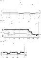
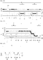
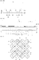
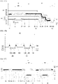
- FIGS. 1 and 2 are views schematically showing a touch display apparatus according to an embodiment of the present disclosure.
- FIG. 3 is an enlarged view of K region in FIG. 2 .
- FIG. 4A is a view taken along I-I' of FIG. 2 .
- FIG. 4B is a view taken along II-II' of FIG. 2 .
- FIG. 4C is a view taken along III-III' of FIG. 3 .
- the touch display apparatus may include a device substrate 110.
- the device substrate 110 may include an insulating material.
- the device substrate 110 may include glass or plastic.
- the device substrate 110 may include a display area AA and a bezel area BZ disposed outside the display area AA.
- the bezel area BZ may surround the display area AA.
- the display area AA of the device substrate 110 may realize an image provided to a user.
- a plurality of pixel areas PA may be disposed in the display area AA of the device substrate 110.
- the pixel areas PA may be disposed side by side in a first direction and a second direction perpendicular to the first direction. Two of the pixel areas PA adjacent in the first direction may be alternately disposed. Two of the pixel areas PA adjacent in the second direction may be alternately disposed.
- Each of the pixel areas PA may realize a color different from adjacent pixel areas PA.
- the touch display apparatus according to the embodiment of the present disclosure may include a first row in which red pixel regions R and blue pixel regions B are alternately positioned and a second row in which green pixel regions G are disposed.
- the touch display apparatus according to the embodiment of the present disclosure may have a pentile structure in which the first row and the second row are alternately repeated.
- Each of the pixel areas PA may emit light displaying a specific color.
- a pixel driving circuit and a light-emitting device 130 electrically connected to the pixel driving circuit may be disposed in each pixel area PA.
- the pixel driving circuit may be connected to one of gate lines GL applying a gate signal and one of data lines DL applying a data signal.
- the pixel driving circuit may generate a driving current corresponding to the data signal according to the scan signal.
- the driving current generated by the pixel driving circuit may provide to the light-emitting device 130, during one frame.
- the pixel driving circuit may include a switching thin film transistor T1, a driving thin film transistor T2 and a storage capacitor Cst.
- the switching thin film transistor T1 may provide the data signal to the driving thin film transistor T2 according to the scan signal.
- the driving thin film transistor T2 may generate the driving current corresponding to the data signal.
- the driving thin film transistor T2 may include a semiconductor pattern 121, a gate insulating layer 122, a gate electrode 123, a source electrode 124 and a drain electrode 125.
- the semiconductor pattern 121 may include a semiconductor material.
- the semiconductor pattern 121 may include at least one of amorphous silicon, polycrystalline silicon and oxide semiconductor.
- the semiconductor pattern 121 may include a source region, a drain region and a channel region.
- the channel region may be disposed between the source region and the drain region.
- the source region and the drain region may have a lower resistance than the channel region.
- the source region and the drain region may include a conductorized region of the oxide semiconductor.
- the gate insulating layer 122 may be disposed on the semiconductor pattern 121.
- the gate insulating layer 122 may overlap the channel region of the semiconductor pattern 121.
- the source region and the drain region of the semiconductor pattern 121 may be disposed outside the gate insulating layer 122.
- the gate insulating layer 122 may include an insulating material.
- the gate insulating layer 122 may include an inorganic insulating material, such as silicon oxide (SiO) and silicon nitride (SiN).
- the gate electrode 123 may be disposed on the gate insulating layer 122.
- the gate electrode 123 may overlap the channel region of the semiconductor pattern 121.
- the gate electrode 123 may be insulated from the semiconductor pattern 121 by the gate insulating layer 122.
- a side of the gate insulating layer 122 may be continuous with a side of the gate electrode 123.
- the gate electrode 123 may include a conductive material.
- the gate electrode 123 may include a metal, such as aluminum (Al), titanium (Ti), copper (Cu), molybdenum (Mo), tantalum (Ta), chromium (Cr) and tungsten (W).
- the channel region of the semiconductor pattern 121 may have an electric conductivity corresponding to a voltage applied to the gate electrode 123.
- the source electrode 124 may include a conductive material.
- the source electrode 124 may include a metal, such as aluminum (Al), titanium (Ti), copper (Cu), molybdenum (Mo), tantalum (Ta), chromium (Cr) or tungsten (W).
- the source electrode 124 may be insulated from the gate electrode 123.
- the source electrode 124 may be disposed on a layer different from the gate electrode 123.
- an interlayer insulating layer 112 covering the gate electrode 123 may be disposed on the device substrate 110, and the source electrode 124 may be disposed on the interlayer insulating layer 112.
- the interlayer insulating layer 112 may include an insulating material.
- the interlayer insulating layer 112 may include an inorganic insulating material, such as silicon oxide (SiO) and silicon nitride (SiN).
- the source electrode 124 may include a material different from the gate electrode 123.
- the source electrode 124 may be electrically connected to the source region of the semiconductor pattern 121.
- the interlayer insulating layer 112 may include a source contact hole partially exposing the source region of the semiconductor pattern 121.
- the source electrode 124 may be in direct contact with the source region of the semiconductor pattern 121 through the source contact hole.
- the drain electrode 125 may include a conductive material.
- the drain electrode 125 may include a metal, such as aluminum (Al), titanium (Ti), copper (Cu), molybdenum (Mo), tantalum (Ta), chromium (Cr) or tungsten (W).
- the drain electrode 125 may be insulated from the gate electrode 123.
- the drain electrode 125 may be disposed on a layer different from the gate electrode 123.
- the drain electrode 125 may be disposed on the interlayer insulating layer 112.
- the drain electrode 125 may be disposed on the same layer as the source electrode 124.
- the drain electrode 125 may include the same material as the source electrode 124.
- the drain electrode 125 may be formed simultaneously with the source electrode 124.
- the drain electrode 125 may include a material different from the gate electrode 123.
- the drain electrode 125 may be electrically connected to the drain region of the semiconductor pattern 121.
- the interlayer insulating layer 112 may include a drain contact hole partially exposing the drain region of the semiconductor pattern 121.
- the drain electrode 125 may be in direct contact with the drain region of the semiconductor pattern 121 through the drain contact hole.
- the switching thin film transistor T1 may have the same structure as the driving thin film transistor T2.
- the switching thin film transistor T1 may include a gate electrode being electrically connected to the corresponding gate line GL, a source electrode being electrically connected to the corresponding data line DL, and a drain electrode being electrically connected to the gate electrode 123 of the driving thin film transistor T2.
- the source electrode 124 of the driving thin film transistor T2 may be connected to a first power voltage supply line VDD which supplies a positive power voltage.
- the storage capacitor Cst may maintain a voltage applied to the gate electrode 123 of the driving thin film transistor T2 during one frame.
- the storage capacitor Cst may be connected between the gate electrode 123 and the drain electrode 125 of the driving thin film transistor T2.
- the light-emitting device 130 may emit light using the driving current supplied from the pixel driving circuit.
- the light-emitting device 130 may include a first emission electrode 131, a light-emitting stack 132 and a second emission electrode 133, which are sequentially stacked on the device substrate 110.
- the first emission electrode 131 may be electrically connected to the drain electrode 125 of the driving thin film transistor T2.
- the driving current generated by the pixel driving circuit may be supplied to the first emission electrode 131 of the light-emitting device 130.
- the first emission electrode 131 may include a conductive material.
- the first emission electrode 131 may include a material having high reflectance.
- the first emission electrode 131 may include a metal, such as aluminum (Al), titanium (Ti), copper (Cu), molybdenum (Mo), tantalum (Ta), chromium (Cr) or tungsten (W).
- the first emission electrode 131 may have a multi-layer structure.
- the first emission electrode 131 may include a structure in which a reflective electrode made of a metal is disposed between transparent electrodes made of a transparent conductive material, such as ITO and IZO.
- the light-emitting stack 132 may generate the light having a luminance corresponding to a voltage difference between the first emission electrode 131 and the second emission electrode 133.
- the light-emitting stack 132 may include an emission material layer (EML) having an emission material.
- the emission material may include an organic material, an inorganic material or a hybrid material.
- the touch display apparatus according to the embodiment of the present disclosure may be an organic light-emitting display apparatus including an organic emission material.
- the light-emitting stack 132 may have a multi-layer structure.
- the light-emitting stack 132 may include at least one of a hole injection layer (HIL), a hole transport layer (HTL), an electron transport layer (ETL) and an electron injection layer (EIL).
- the light-emitting stack 132 may include a plurality of the emission material layer.
- the light-emitting stack 132 may include a charge generation layer (CGL) between a first emission material layer and a second emission material layer.
- the second emission material layer may include a material different from the first emission material layer.
- the second emission electrode 133 may include a conductive material.
- the second emission electrode 133 may have a transmittance higher than the first emission electrode 131.
- the second emission electrode 133 may be a transparent electrode made of a transparent conductive material.
- the second emission electrode 133 may include a transparent conductive oxide, such as ITO, IZO and AZO.
- a device buffer layer 111 may be disposed between the device substrate 110 and the pixel driving circuit of each pixel area PA.
- the device buffer layer 111 may prevent pollution due to the device substrate 110 in a process of forming the pixel driving circuits.
- the device buffer layer 111 may extend onto the bezel area BZ of the device substrate 110.
- an upper surface of the device substrate 110 toward the pixel driving circuit of each pixel area PA may be completely covered by the device buffer layer 111.
- the device buffer layer 111 may include an insulating material.
- the device buffer layer 111 may include an inorganic insulating material, such as silicon oxide (SiO) and silicon nitride (SiN).
- the device buffer layer 111 may have a multi-layer structure.
- the device buffer layer 111 may have a stacked structure of an inorganic insulating layer made of silicon oxide (SiO) and an inorganic insulating layer made of silicon nitride (SiN).
- a planarization layer 113 may be disposed between the pixel driving circuit and the light-emitting device 130 of each pixel area PA.
- the planarization layer 113 may remove a thickness difference due to the pixel driving circuit of each pixel area PA.
- an upper surface of the planarization layer 113 opposite to the device substrate 110 may be a flat surface.
- the switching thin film transistor T1, the driving thin film transistor T2 and the storage capacitor Cst in each pixel area PA may be covered by the planarization layer 113.
- the planarization layer 113 may include an insulating material.
- the planarization layer 113 may include a material different from the interlayer insulating layer 112.
- the planarization layer 113 may include an organic insulating material.
- the first emission electrode 131 of each pixel area PA may be electrically connected to the pixel driving circuit of the corresponding pixel area PA by penetrating the planarization layer 113.
- the planarization layer 113 may include pixel contact holes partially exposing the drain electrode 125 of the driving thin film transistor T2 in each pixel area PA.
- the first emission electrode 131 of each pixel area PA may be in direct contact with the drain electrode 125 of the driving thin film transistor T2 in the corresponding pixel area PA through one of the pixel contact holes.
- the first emission electrode 131 of each pixel area PA may be insulated from the first emission electrode 131 of adjacent pixel area PA.
- the first emission electrode 131 of each pixel area PA may be spaced away from the first emission electrode 131 of adjacent pixel area PA.
- a bank insulating layer 114 may be disposed between the first emission electrodes 131 of adjacent pixel areas PA.
- the bank insulating layer 114 may include an insulating material.
- the bank insulating layer 114 may include an organic insulating material.
- the bank insulating layer 114 may cover an edge of the first emission electrode 131 in each pixel area PA.
- the light-emitting stack 132 and the second emission electrode 133 of each pixel area PA may be stacked on a portion of the corresponding first emission electrode 131 exposed by the bank insulating layer 114.
- the bank insulating layer 114 may define an emission area BEA, GEA and REA in each pixel area PA.
- the light-emitting device 130 of each pixel area PA may have the same structure as the light-emitting device 130 of adjacent pixel area PA.
- the light-emitting stack 132 of each pixel area PA may be connected to the light-emitting stack 132 of adjacent pixel area PA by extending along a surface of the bank insulating layer 114.
- the light emitted from the light-emitting device 130 of each pixel area PA may display the same color as the light emitted from the light-emitting device 130 of adjacent pixel area PA.
- the light-emitting stack 132 of each pixel area PA may generate white light.
- the light-emitting stack 132 of each pixel area PA may be formed simultaneously with the light-emitting stack 132 of adjacent pixel area PA.
- a process of forming the light-emitting stack 132 on each pixel area PA may be simplified.
- a voltage applied to the second emission electrode 133 of each pixel area PA may be the same as a voltage applied to the second emission electrode 133 of adjacent pixel area PA.
- the second emission electrode 133 of each pixel area PA may be electrically connected to a second power voltage supply line VSS which supplies a negative power voltage.
- VSS second power voltage supply line
- the luminance of the light emitted from the light-emitting device 130 of each pixel area PA may be adjusted by the data signal applied to the corresponding pixel area PA.
- the second emission electrode 133 of each pixel area PA may be electrically connected to the second emission electrode 133 of adjacent pixel area PA.
- the second emission electrode 133 of each pixel area PA may be in direct contact with the second emission electrode 133 of adjacent pixel area PA.
- the second emission electrode 133 of each pixel area PA may be formed simultaneously with the second emission electrode 133 of adjacent pixel area PA. Therefore, in the touch display apparatus according to the embodiment of the present disclosure, a process of forming the second emission electrode 133 on each pixel area PA may be simplified.
- An encapsulating unit 140 may be disposed on the light-emitting device 130 of each pixel area PA.
- the encapsulating unit 140 may prevent the damage of the light-emitting devices 130 to external moisture and/or oxygen.
- the light-emitting device 130 of each pixel area PA may be completely covered by the encapsulating unit 140.
- the encapsulating unit 140 may extend onto the bezel area BZ of the device substrate 110.
- the encapsulating unit 140 may include at least one inorganic encapsulating layer 141 and 143 and at least one organic encapsulating layer 142.
- the encapsulating unit 140 may have a structure in which at least one organic encapsulating layer 142 is disposed between inorganic encapsulating layers 141 and 143.
- the uppermost layer of the encapsulating unit 140 may be the inorganic encapsulating layer 141 and 143.
- an upper surface and a side of the organic encapsulating layer 142 may be covered by the inorganic encapsulating layer 141 and 143.
- the inorganic encapsulating layer 141 and 143 may include an inorganic insulating material.
- the inorganic encapsulating layer 141 and 143 may include an inorganic insulating material capable of low-temperature deposition, such as silicon nitride (SiN), silicon oxide (SiO), silicon oxy-nitride (SiON) and aluminum oxide (Al 2 O 3 ).
- SiN silicon nitride
- SiO silicon oxide
- SiON silicon oxy-nitride
- Al 2 O 3 aluminum oxide
- the organic encapsulating layer 142 may relieve stress due to the inorganic encapsulating layer 141 and 143.
- the organic encapsulating layer 142 may include an organic insulating material, such as acryl resin, epoxy resin, poly-imide, poly-ethylene and silicon oxycarbide (SiOC).
- a thickness difference due to the light-emitting devices 130 may be removed by the organic encapsulating layer 142.
- an upper surface of the organic encapsulating layer 144 opposite to the device substrate 110 may be a flat surface.
- the organic encapsulating layer 142 may be formed by an ink-jet method.
- at least one dam 106 may be disposed on the bezel area BZ of the device substrate 110.
- the dam 106 may block the flow of the organic encapsulating layer 142.
- the dam 106 may extend along an edge of the display area AA.
- the organic encapsulating layer 142 may be formed in a region defined by the dam 106.
- the dam 106 may be formed using a process of forming at least one of insulating layers, which are disposed between the device substrate 110 and the encapsulating unit 140.
- the dam 106 may be formed simultaneously with the planarization layer 113.
- the dam 106 may include the same material as the planarization layer 113.
- the dam 106 may include an organic insulating material.
- the interlayer insulating layer 112 may extend onto the bezel area BZ of the device substrate 110.
- the dam 106 may be disposed on the interlayer insulating layer 112.
- a thickness of the dam 106 may be the same as a thickness of the planarization layer 113.
- a touch sensor Cm may be disposed on the encapsulating unit 140.
- the touch sensor Cm may sense the touch of the user and/or the tool.
- the touch sensor Cm may detect the presence or the absence of the touch and the location of the touch through a change in mutual capacitance.
- the touch sensor Cm may include a first touch line 310 and a second touch line 320.
- a touch driving signal may be applied to the first touch line 310.
- the first touch line 310 may function as a touch driving line.
- the first touch line 310 may include first touch electrodes 311 and first bridge electrodes 312.
- the first touch electrodes 311 may be disposed side by side on the encapsulating unit 140.
- the first bridge electrodes 312 may be electrically connected between the first touch electrodes 311.
- Each of the first bridge electrodes 312 may extend in a first direction.
- each of the first touch electrodes 311 may be connected to adjacent first touch electrodes 311 in the first direction by one of the first bridge electrodes 312.
- the first touch electrodes 311 may include a conductive material.
- the first touch electrodes 311 may include a material having a relative low resistance.
- the first touch electrodes 311 may include a metal, such as titanium (Ti), copper (Cu), molybdenum (Mo) and tantalum (Ta).
- Each of the first touch electrodes 311 may have a multi-layer structure.
- the first touch electrodes 311 may have a three-layer structure, such as Ti/Al/Ti, MoTi/Cu/MoTi and Ti/Al/Mo.
- the first bridge electrodes 312 may include a conductive material.
- the first bridge electrodes 312 may include a material having a relative low resistance.
- the first bridge electrodes 312 may include a metal, such as titanium (Ti), copper (Cu), molybdenum (Mo) and tantalum (Ta).
- the first bridge electrodes 312 may include the same material as the first touch electrodes 311.
- Each of the first bridge electrodes 312 may have a multi-layer structure.
- the first bridge electrodes 312 may have a three-layer structure, such as Ti/Al/Ti, MoTi/Cu/MoTi and Ti/Al/Mo.
- the first bridge electrodes 312 may have the same structure as the first touch electrodes 311.
- the first bridge electrodes 312 may be disposed on the same layer as the first touch electrode 311.
- each of the first bridge electrodes 312 may be in direct contact with the first touch electrodes 311.
- the second touch line 320 may include second touch electrodes 321 and second bridge electrodes 322.
- the second touch electrodes 321 may be disposed side by side on the encapsulating unit 140.
- the second touch electrodes 321 may be disposed on the same layer as the first touch electrodes 311.
- the second touch electrodes 321 may be insulated from the first touch electrodes 311.
- the second touch electrodes 321 may be disposed between the first touch electrodes 311.
- the second touch electrodes 321 may have the same shape as the first touch electrodes 311.
- the first touch electrodes 311 and the second touch electrodes 321 may be disposed on the encapsulating unit 140, alternately.
- the touch display apparatus may detect the touch of the user and/or the tool and the location of the touch using the touch sensor Cm.
- the second touch electrodes 321 may include a conductive material.
- the second touch electrodes 321 may include a material having a relative low resistance.
- the second touch electrodes 321 may include a metal, such as titanium (Ti), copper (Cu), molybdenum (Mo) and tantalum (Ta).
- Each of the second touch electrodes 321 may have a multi-layer structure.
- the second touch electrodes 321 may have a three-layer structure, such as Ti/Al/Ti, MoTi/Cu/MoTi and Ti/Al/Mo.
- the second touch electrodes 321 may be disposed on the same layer as the first touch electrodes 311 and the first bridge electrodes 312.
- the second touch electrodes 321 may be insulated from the first bridge electrodes 312.
- the second touch electrodes 321 may be spaced away from the first bridge electrodes 312.
- the first bridge electrodes 312 may cross between the second touch electrodes 321.
- the second bridge electrodes 322 may be electrically connected between the second touch electrodes 321. Each of the second bridge electrodes 322 may extend in a second direction. For example, each of the second touch electrodes 321 may be connected to adjacent second touch electrodes 321 in the second direction by one of the second bridge electrodes 322. The second direction may be different from the first direction. For example, the second direction may be perpendicular to the first direction. The second bridge electrodes 322 may cross between the first touch electrodes 311. For example, each of the second bridge electrodes 322 may cross one of the first bridge electrodes 311. The second bridge electrodes 322 may be insulated from the first bridge electrodes 312. The second bridge electrodes 322 may be disposed on a layer different from the first bridge electrodes 312.
- the touch sensor Cm may include a touch insulating layer 350 disposed on the second bridge electrodes 322, and the first touch electrodes 311, the first bridge electrodes 312 and the second touch electrodes 322 may be disposed on the touch insulating layer 350.
- the touch insulating layer 350 may include an insulating material.
- the touch insulating layer 350 may include an inorganic insulating material, such as silicon oxide (SiO) and silicon nitride (SiN).
- the touch insulating layer 350 may include touch contact holes partially exposing each second bridge electrode 322.
- Each of the second touch electrodes 321 may be connected to the corresponding second bridge electrode 322 through one of the touch contact holes.
- the second bridge electrodes 322 may include a conductive material.
- the second bridge electrodes 322 may include a material having a relative low resistance.
- the second bridge electrodes 322 may include a metal, such as titanium (Ti), copper (Cu), molybdenum (Mo) and tantalum (Ta).
- Each of the second bridge electrodes 322 may have a multi-layer structure.
- the second bridge electrodes 322 may have a three-layer structure, such as Ti/Al/Ti, MoTi/Cu/MoTi and Ti/Al/Mo.
- the first touch electrodes 311, the first bridge electrodes 312, the second touch electrodes 321 and the second bridge electrodes 322 of the touch sensor Cm may be disposed in the display area AA of the device substrate 110.
- the emission area BEA, GEA and REA of each pixel area PA may be disposed among the first touch electrodes 311, the first bridge electrodes 312, the second touch electrodes 321 and the second bridge electrodes 322.
- the first touch line 310 and the second touch line 320 may be disposed outside the light-emitting devices 130.
- the first touch electrodes 311, the first bridge electrodes 312, the second touch electrodes 321 and the second bridge electrodes 322 may overlap the bank insulating layer 114.
- each first touch electrode 311 and the planar shape of each second touch electrode 321 may be a mesh shape including openings overlapping with the emission area BEA, GEA and REA of each pixel area PA.
- the accuracy of touch sensing using the touch sensor Cm may be improved, the decrease in lightextraction efficiency due to the first touch electrodes 311, the first bridge electrodes 312, the second touch electrodes 321 and the second bridge electrodes 322 of the touch sensor Cm may be reduced.
- a touch buffer layer 200 may be disposed between the encapsulating unit 140 and the touch sensor Cm.
- the second bridge electrodes 322 may be disposed between the touch buffer layer 200 and the touch insulating layer 350.
- the touch buffer layer 200 may reduce the parasitic capacitance generated between the second emission electrode 133 of each light-emitting device 130 and the touch sensor Cm.
- the distance between the first touch line 310 of the touch sensor Cm and the second emission electrode 133 of each light-emitting device 130 and a distance between the second touch line 320 of the touch sensor Cm and the second emission electrode 133 of each light-emitting device 130 may be increased by the touch buffer layer 200.
- the touch buffer layer 200 may include an insulating material.
- the touch buffer layer 200 may include an inorganic insulating material, such as silicon oxide (SiO) and silicon nitride (SiN).
- a black matrix 410 may be disposed on the first touch electrodes 311, the first bridge electrodes 312 and the second touch electrodes 321 of the touch sensor Cm.
- the black matrix 410 may overlap the first touch electrodes 311, the first bridge electrodes 312 and the second touch electrodes 321.
- an upper surface of each first touch electrode 311, an upper surface of each first bridge electrode 312 and an upper surface of each second touch electrode 321, which are opposite to the device substrate 110 may be covered by the black matrix 410.
- the black matrix 410 may be in direct contact with the upper surface of each first touch electrode 311, the upper surface of each first bridge electrode 312 and the upper surface of each second touch electrode 321.
- the planar shape of the black matrix 410 in the display area AA of the device substrate 110 may be the same as the planar shape by the first touch electrodes 311, the first bridge electrodes 312 and the second touch electrodes 321.
- a side of the black matrix 410 may be continuous with a side of each first touch electrode 311, a side of each first bridge electrode 312 and a side of each second touch electrode 321.
- the black matrix 410 may be disposed outside the light-emitting devices 130.
- the planar shape of the black matrix 410 may be a mesh shape.
- the black matrix 410 may include a gap 410g overlapping with a spaced region between the first touch electrodes 311 and the second touch electrodes 321.
- the black matrix 410 may block the light.
- the external light travelling toward the first touch electrodes 311, the first bridge electrodes 312 and the second touch electrodes 321 may be blocked by the black matrix 410. Therefore, in the touch display apparatus according to the embodiment of the present disclosure, the reflection of the external light by the first touch electrodes 311, the first bridge electrodes 312 and the second touch electrodes 321 of the touch sensor Cm may be prevented.
- Color filters 420b, 420g and 420r overlapping with the emission areas BEA, GEA and REA may be disposed on the encapsulating unit 140.
- the color filters 420b, 420g and 420r may overlap the light-emitting device 130.
- the light generated by each light-emitting device 130 may emitted to the outside through one of the color filters 420b, 420g and 420r.
- Each of the color filters 420b, 420g, 420r may include a material different from adjacent color filter 420b, 420g and 420r.
- blue color filters 420b may be disposed on blue emission areas BEA of blue pixel areas B
- green color filters 420g may be disposed on green emission areas GEA of green pixel areas G
- red color filters 420r may be disposed on red emission areas REA of red pixel areas R.
- the touch display apparatus may provide the image made of various colors to the user using white color emitted from the light-emitting device 130 of each pixel area PA and the color filters 420b, 420g and 420r.
- the color filters 420b, 420g and 420r may be disposed in the openings of the first touch electrodes 311 and the second touch electrodes 321, which have a mesh shape.
- the black matrix 410 may surround the color filters 420b, 420g and 420r.
- the external light which is not blocked by the black matrix 410 may be irradiated to the light-emitting devices 130 through one of the color filters 420b, 420g and 420r.
- the external light reflected by the first emission electrode 131 of each light-emitting device 130 may be emitted to the outside through the color filter 420b, 420g and 420r overlapping with the corresponding light-emitting device 130. That is, in the touch display apparatus according to the embodiment of the present disclosure, the external light reflected by the first emission electrode 131 of each light-emitting device 130 may display the same color as the light emitted from the corresponding light-emitting device 130. Therefore, in the touch display apparatus according to the embodiment of the present disclosure, the deterioration of the image due to the reflection of the external light may be prevented, without using a polarizing plate.
- a touch passivation layer 500 may be disposed on the black matrix 410 and the color filters 420b, 420g and 420r.
- the touch passivation layer 500 may prevent the damage of the touch sensor Cm, the black matrix 410 and the color filters 420b, 420g and 420r due to the external impact and/or moisture.
- the touch passivation layer 500 may extend beyond the display area AA.
- the first touch electrodes 311, the first bridge electrodes 312, the second touch electrodes 321, the black matrix 410 and the color filters 420b, 420g and 420r may be completely covered by the touch passivation layer 500.
- the touch passivation layer 500 may include an insulating material.
- the touch passivation layer 500 may include a material different from the touch insulating layer 350.
- the touch passivation layer 500 may include an organic insulating material. A thickness difference due to the first touch line 310, the second touch line 320, the black matrix 410 and the color filters 420b, 420g and 420r may be removed by the touch passivation layer 500.
- a cover element 600 may be disposed on the touch passivation layer 500.
- the cover element 600 may prevent the damage due to the external impact.
- the cover element 600 may be in direct contact with the touch passivation layer 500.
- the cover element 600 may include a cover adhesive layer 610 and a cover window 620.
- the cover adhesive layer 610 may include an adhesive material.
- the cover adhesive layer 610 may include a transparent material.
- the cover adhesive layer 610 may include an optical clear adhesive (OCA).
- OCA optical clear adhesive
- the cover adhesive layer 610 may relieve the reflection of the external light.
- the cover adhesive layer 610 may include a dye.
- the cover window 620 may be attached to the touch passivation layer 500 by the cover adhesive layer 610.
- the cover window 620 may include a transparent material.
- the cover window 620 may have a hardness greater than or equal to a specific level.
- the cover window 620 may include glass or plastic.
- the bezel area BZ of the device substrate 110 may include a pad area PD in which display pads 104 and touch pads 304 are disposed.
- the dam 106 may be disposed between the display area AA and the pad area PD.
- the display pads 104 and the touch pads 304 may be spaced away from the encapsulating unit 140.
- a portion of the display pads 104 and the touch pads 304 may be prevented from being unintentionally covered by the organic encapsulating layer 142. Therefore, in the touch display apparatus according to the embodiment of the present disclosure, the distortion of the signal transmitted through the display pads 104 and the touch pads 304 may be prevented.
- the gate lines GL and/or the data lines DL may be electrically connected to the display pads 104.
- the data signal applied to each pixel area PA may be transmitted by one of the display pads 104 and one of the data lines DL.
- Each of the display pads 104 may include a first lower pad electrode 104a and a first upper pad electrode 104b on the first lower pad electrode 104a.
- the display pads 104 may be formed using a process of forming the pixel driving circuits, the light-emitting devices 130 and the touch sensor Cm.
- the first lower pad electrode 104a may include the same material as the source electrode 124 and the drain electrode 125 of each pixel driving circuit
- the first upper pad electrode 104b may include the same material as the first touch electrodes 311, the first bridge electrodes 312 and the second touch electrodes 321.
- the touch pads 304 may be disposed side by side the display pads 104.
- the pad area PD may be disposed on a side of the display area AA.
- the touch pads 304 may have the same structure as the display pads 104.
- each of the touch pads 304 may include a second lower pad electrode 304a and a second upper pad electrode 304b on the second lower pad electrode 304a.
- the touch pads 304 may be formed simultaneously with the display pads 104.
- the second lower pad electrode 304a may include the same material as the first lower pad electrode 104a
- the second upper pad electrode 304b may include the same material as the first upper pad electrode 104b.
- the touch pads 304 may be electrically connected to the first touch line 310 and the second touch line 320 through touch routing lines 330.
- the touch driving signal may be applied to the first touch line 310 through one of the touch pads 304 and one of the touch routing lines 330, the charges charged by the touch driving signal may be discharged through the second touch line 320, one of the touch routing lines 330 and one of the touch pads 304.
- the touch routing lines 330 may be formed using a process of forming the touch sensor Cm.
- each of the touch routing lines 330 may have a stacked structure of a lower routing line 331 including the same material as the second bridge electrodes 322 and an upper routing line 332 including the same material as the first bridge electrodes 312.
- the upper routing line 332 of each touch routing line 330 may be electrically connected to the lower routing line 331 of the corresponding touch routing line 330.
- the touch insulating layer 350 may include routing contact holes partially exposing the lower routing line 331 of each touch routing line 330.
- the upper routing line 332 of each touch routing line 330 may be in direct contact with the lower routing line 331 of the corresponding touch routing line 330 through the routing contact holes.
- the first touch line 310 and the second touch line 320 may be stably connected to the corresponding touch pad 304 by the touch routing lines 330. And, in the touch display apparatus according to the embodiment of the present disclosure, the resistance of each touch routing line 330 may be reduced. Therefore, in the touch display apparatus according to the embodiment of the present disclosure, a signal delay caused by the touch routing lines 330 may be minimized.
- the device buffer layer 111, the interlayer insulating layer 112, the touch buffer layer 200, the touch insulating layer 350, the black matrix 410 and the touch passivation layer 500 may extend onto the pad area PD of the device substrate 110.
- the first lower pad electrode 104a and the second lower pad electrode 304a may be disposed on the interlayer insulating layer 112, and the touch buffer layer 200 and the touch insulating layer 350 may include pad contact holes partially exposing the first lower pad electrode 104a of each display pad 104 and the second lower pad electrode 304a of each touch pad 304.
- the first upper pad electrode 104b of each display pad 104 may be electrically connected to the first lower pad electrode 104a of the corresponding display pad 104 by one of the pad contact holes
- the second upper pad electrode 304b of each touch pad 304 may be electrically connected to the second lower pad electrode 304a of the corresponding touch pad 304 by one of the pad contact holes.
- the black matrix 410 may overlap the touch routing lines 330.
- an upper surface of each touch routing line 330 opposite to the device substrate 110 may be covered by the black matrix 410.
- the black matrix 410 may extend parallel to the touch routing lines 330.
- the planar shape of the black matrix 410 between the display area AA and the pad area PD may be the same as the planar shape of the touch routing lines 330.
- the black matrix 410 may be in direct contact with the touch routing lines 330.
- a side of the upper routing line 332 of each touch routing line 330 may be continuous with the side of the black matrix 410.
- the touch passivation layer 500 may include first pad open holes 501h overlapping with a center region of the first upper pad electrode 104b of each display pad 104 and second pad open holes 502h overlapping with a center region of the second upper pad electrode 304b of each touch pad 304.
- the black matrix 410 may include first pad apertures 411h overlapping with the first pad open holes 501h and second pad apertures 412h overlapping with the second pad open holes 502h.
- first upper pad electrode 104b of each display pad 104 may be partially exposed by one of the first pad apertures 411h and one of the first pad open holes 501h
- second upper pad electrode 304b of each touch pad 304 may be partially exposed by one of the second pad apertures 412h and one of the second pad open holes 502h
- Each of the first upper pad electrodes 104b and the second upper pad electrodes 304b may include an upper surface opposite to the device substrate 110, and the black matrix 410 and the touch passivation layer 500 may be stacked on an edge of the upper surface of the first upper pad electrode 104b of each display pad 104 and an edge of the upper surface of the second upper pad electrode 304b of each touch pad 304.
- the black matrix 410 may include a material having greater adhesion to the first upper pad electrode 104b and the second upper pad electrode 304b than the touch passivation layer 500.
- peeling of the touch passivation layer 500 covering the edge of the first upper pad electrode 104b of each display pad 104 and the edge of the second upper pad electrode 304b of each display pad 304 may be prevented by the black matrix 410. Therefore, in the touch display apparatus according to the embodiment of the present disclosure, the penetration of the external moisture through the edge of the first upper pad electrode 104b of each display pad 104 and the edge of the second upper pad electrode 304b of each touch pad 304 may be prevented.
- FIGS. 5A to 11A, 5B to 11B and 5C to 11C are views sequentially showing a method of forming the touch display apparatus according to the embodiment of the present disclosure.
- the method of forming the touch display apparatus may include a step of forming pixel driving circuit including a driving thin film transistor T2, at least one dam 106, a device buffer layer 111, an interlayer insulating layer 112, a planarization layer 113, a bank insulating layer 114, light-emitting device 130, a first lower pad electrode 104a and a second lower pad electrode 304a on a device substrate 110, and a step of forming an encapsulating unit 140 on the pixel driving circuits and the light-emitting device 130.
- the device substrate 110 may include a display area AA and a bezel area BZ disposed outside the display area AA.
- the bank insulating layer 114 may define emission areas BEA, GEA and REA in the display area AA.
- the bezel area BZ may include a pad area PD.
- the pixel driving circuits and the light-emitting devices 130 may be formed on the display area AA of the device substrate 110.
- the first lower pad electrode 104a and the second lower pad electrode 304a may be formed in the pad area PD.
- the device buffer layer 111 and the interlayer insulating layer 112 may extend onto the bezel area BZ of the device substrate 110.
- first lower pad electrode 104a and the second lower pad electrode 304a may be formed on the interlayer insulating layer 112.
- the first lower pad electrode 104a and the second lower pad electrode 304a may be formed using a process of forming the pixel driving circuits.
- the first lower pad electrode 104a and the second lower pad electrode 304a may be formed simultaneously with the source electrode 124 and the drain electrode 125 of the driving thin film transistor T2 of each pixel driving circuit.
- the encapsulating unit 140 may be formed in a region defined by the dam 106.
- the dam 106 may be formed between the display area AA and the pad area PD.
- the first lower pad electrode 104a and the second lower pad electrode 304a formed in the pad area PD may be spaced away from the encapsulating unit 140.
- the method of forming the touch display apparatus may include a step of forming a touch buffer layer 200 on the device substrate 110 in which the encapsulating unit 140, the first lower pad electrode 104a and the second lower pad electrode 304a are formed, and a step of forming second bridge electrodes 322 and lower routing lines 331 on the touch buffer layer 200.
- the touch buffer layer 200 may cover the first lower pad electrode 104a and the second lower pad electrode 304a.
- the step of forming the touch buffer layer 200 may include a step of depositing an inorganic insulating material on the entire surface of the device substrate 110 in which the encapsulating unit 140, the first lower pad electrode 104a and the second lower pad electrode 304a are formed.
- the second bridge electrodes 322 may be formed on the display area AA of the device substrate 110.
- the second bridge electrodes 322 may be formed outside the emission areas BEA, GEA and REA.
- the second bridge electrodes 322 may overlap the bank insulating layer 114.
- the lower routing lines 331 may be formed between the display area AA and the second bridge electrodes 322.
- the lower routing lines 331 may be formed simultaneously with the second bridge electrodes 322.
- a step of forming the second bridge electrodes 322 and the lower routing lines 331 may include a step of forming a conductive material layer on the touch buffer layer 200 and a step of patterning the conductive material layer.
- the lower routing lines 331 may include the same material as the second bridge electrodes 322.
- the lower routing lines 331 and the second bridge electrodes 322 may be formed of a metal, such as titanium (Ti), copper (Cu), molybdenum (Mo) and tantalum (Ta).
- the lower routing lines 331 and the second bridge electrodes 322 may have a multi-layer structure.
- the lower routing lines 331 and the second bridge electrodes 322 may have a three-layer structure, such as Ti/Al/Ti, MoTi/Cu/MoTi and Ti/Al/Mo.
- the lower routing lines 331 may have a stacked structure same as the second bridge electrodes 322.
- the method of forming the touch display apparatus may include a step of forming a touch insulating layer 350 on the device substrate 110 in which the second bridge electrodes 322 and the lower routing lines 331 are formed.
- the touch insulating layer 350 may expose a portion of each second bridge electrode 322.
- the touch insulating layer 350 may partially expose each lower routing line 331.
- the touch insulating layer 350 may expos a portion of each first lower pad electrode 104a and a portion of each second lower pad electrode 304a.
- the step of forming the touch insulating layer 350 may include a step of forming an insulating layer on the display area AA and the bezel area BZ of the device substrate 110 and a step of patterning the insulating layer.
- a step of exposing the portion of each first lower pad electrode 104a and the portion of each second lower pad electrode 304a may include a step of forming pad contact holes penetrating the touch buffer layer 200 and the touch insulating layer 350.
- the pad contact holes may be formed by etching the touch insulating layer 350 and the touch buffer layer 200 on the portion of each first lower pad electrode 104a and the portion of each second lower pad electrode 304a.
- the method of forming the touch display apparatus may include a step of forming a touch conductive layer 300a on the device substrate 110 in which the touch insulating layer 350, and a step of forming a black material layer 400a on the touch conductive layer 300a.
- the touch conductive layer 300a may be formed of a conductive material.
- the touch conductive layer 300a may be formed of a material having a relative low resistance.
- the touch conductive layer 300a may be formed of a metal, such as titanium (Ti), copper (Cu), molybdenum (Mo) and tantalum (Ta).
- the touch conductive layer 300a may have a multi-layer structure.
- the touch conductive layer 300a may have a three-layer structure, such as Ti/Al/Ti, MoTi/Cu/MoTi and Ti/Al/Mo.
- each second bridge electrode 322, the portion of each lower routing line 331, the portion of each first lower pad electrode 104a and the portion of each second lower pad electrode 304a exposed by the touch insulating layer 350 may be in direct contact with the touch conductive layer 300a.
- the black material layer 400a may be formed of a material capable of blocking light.
- the black material layer 400a may include a black dye, such as carbon black.
- the method of forming the touch display apparatus may include a step of forming first touch electrodes 311, first bridge electrodes 312, second touch electrodes 321, upper routing lines 332, first upper pad electrodes 104b, second upper pad electrodes 304b and black matrix 410 on the touch insulating layer 350.
- the first touch electrodes 311, the first bridge electrodes 312 and the second touch electrodes 321 may be formed on the display area AA of the device substrate 110.
- the first touch electrodes 311, the first bridge electrodes 312 and the second touch electrodes 321 may be formed outside the emission areas BEA, GEA and REA.
- the first touch electrodes 311, the first bridge electrodes 312 and the second touch electrodes 321 may overlap the bank insulating layer 114.
- the first touch electrodes 311 may be direct contact with the first bridge electrodes 312.
- the first touch electrodes 311 may be connected by the first bridge electrodes 312 in a first direction to form a first touch line.
- the second touch electrodes 321 may be spaced away from the first touch electrodes 311.
- Each of the second touch electrodes 321 may be connected to one of the second bridge electrodes 322.
- the second touch electrodes 321 may be connected by the second bridge electrodes 322 in a second direction perpendicular to the first direction to form a second touch line.
- the first upper pad electrodes 104b and the second upper pad electrodes 304b may be formed on the pad area PD of the device substrate 110.
- the second upper pad electrodes 304b may be spaced away from the first upper pad electrodes 104b.
- Each of the first upper pad electrodes 104b may be connected to one of the first lower pad electrodes 104a through one of the pad contact holes.
- each of the first lower pad electrodes 104a and the first upper pad electrode 104b connected to the corresponding first lower pad electrode 104a may form a display pad 104.
- Each of the second upper pad electrode 304b may be connected to one of the second lower pad electrodes 304a through one of the pad contact holes.
- each of the second lower pad electrodes 304a and the second upper pad electrode 304b connected to the corresponding second lower pad electrode 304a may be form a touch pad 304.
- the upper routing lines 332 may be formed between the display area AA and the pad area PD. Each of the upper routing lines 332 may be connected to one of the lower routing lines 331. For example, each of the lower routing lines 331 and the upper routing line 332 connected to the corresponding lower routing line 331 may form a touch routing line 330 extending along a surface of the encapsulating unit 140.
- the first touch electrodes 311, the first bridge electrodes 312, the second touch electrodes 321, the upper routing lines 332, the first upper pad electrodes 104b and the second upper pad electrodes 304b may be formed using the touch conductive layer 300a.
- the upper routing lines 332, the first upper pad electrodes 104b and the second pad electrodes 304b may be formed simultaneously with the first touch electrodes 311, the first bridge electrodes 312 and the second touch electrodes 321.
- Each of the upper routing lines 332 may be in direct contact with one of the second upper pad electrodes 304b.
- the black matrix 410 may be formed using the black material layer 400a.
- the step of forming the first touch electrodes 311, the first bridge electrodes 312, the second touch electrodes 321, the upper routing lines 332, the first upper pad electrodes 104b, the second upper pad electrodes 304b and the black matrix 410 may include a step of sequentially patterning the black material layer 400a and the touch conductive layer 300a.
- the first touch electrodes 311, the first bridge electrodes 312, the second touch electrodes 321, the upper routing lines 332, the first upper pad electrodes 104b, the second upper pad electrodes 304b and the black matrix 410 may be formed using a single mask pattern.
- the step of forming the first touch electrodes 311, the first bridge electrodes 312, the second touch electrodes 321, the upper routing lines 332, the first upper pad electrodes 104b, the second upper pad electrodes 304b and the black matrix 410 may include a step of forming a mask pattern on the black material layer 400a, a step of forming the black matrix 410 by etching a portion of the black material layer 400a exposed by the mask pattern, and a step of forming the first touch electrodes 311, the first bridge electrodes 312, the second touch electrodes 321, the upper routing lines 332, the first upper pad electrodes 104b, the second upper pad electrodes 304b by removing a portion of the touch conductive layer 300a exposed by the black matrix 410.
- a side of the black matrix 410 may be continuous with a side of each first touch electrode 311, a side of each first bridge electrode 312, a side of each second touch electrode 321, a side of each upper routing line 332, a side of each first upper pad electrode 104b and a side of each second upper pad electrode 304b.
- the planar shape of the black matrix 410 in the display area AA of the device substrate 110 may be the same as the planar shape by the first touch electrodes 311, the first bridge electrodes 312 and the second touch electrodes 321.
- the black matrix 410 in the display area AA may include a gap 410g overlapping with a spaced region between the first touch electrodes 311 and the second touch electrodes 321.
- the planar shape of the black matrix 410 between the display area AA and the pad area PD may be the same as the planar shape of the touch routing lines 330.
- a side of the black matrix 410 on the pad area PD of the device substrate 110 may be flush with a side of each first upper pad electrode 104b and a side of each second upper pad electrode 304b.
- the method of forming the touch display apparatus may include a step of forming color filters 420b, 420g and 420r on the device substrate 110 in which the black matrix 410 is formed, and a step of forming a touch passivation layer 500 on the device substrate 110 in which the color filters 420b, 420g and 420r are formed.
- the color filters 420b, 420g and 420r may be formed on the emission areas BEA, GEA and REA. For example, each of the light-emitting device 130 may overlap one of the color filters 420b, 420g and 420r. Each of the color filters 420b, 420g and 420r may be formed of a material corresponding to a color in which the corresponding emission area BEA, GEA and REA displays.
- the emission areas BEA, GEA and REA may include blue emission areas BEA displaying a blue color, green emission areas GEA displaying a green color and red emission areas REA displaying a red color, and the step of forming the color filters 420b, 420g and 420r may include a step of forming green color filters 420g on the green emission areas GEA, a step of forming red color filters 420r on the red emission areas REA and a step of forming blue color filters 420b on the blue emission areas BEA.
- Each of the color filters 420b, 420g and 420r may be formed to have a size corresponding to the corresponding pixel area PA.
- the color filters 420b, 420g and 420r may be not formed in the spaced region between the first touch electrodes 311 and the second touch electrodes 321 and the gap 410g of the black matrix 410.
- the touch passivation layer 500 may be formed on the black matrix 410 and the color filters 420b, 420g and 420r.
- the black matrix 410 and the color filters 420b, 420g and 420r may be completely covered by the touch passivation layer 500.
- the touch passivation layer 500 may remove a thickness difference due to the black matrix 410 and the color filters 420b, 420g and 420r on the display area AA.
- the step of forming the touch passivation layer 500 may include a step of depositing an organic insulating material on the entire surface of the device substrate 110 in which the black matrix 410 and the color filters 420b, 420g and 420r.
- the method of forming the touch display apparatus may include a step of partially exposing the display pads 104 and the touch pads 304 by partially etching the black matrix 410 and the touch passivation layer 500.
- First pad open holes 501h overlapping with a center region of the first upper pad electrode 104b of each display pad 104 and a second pad open holes 502h overlapping with a center region of the second upper pad electrode 304b of each touch pad 304 may be formed in the touch passivation layer 500.
- First pad apertures 411h overlapping with the first pad open holes 501h and second pad apertures 412h overlapping with the second pad open holes 502h may be formed in the black matrix 410.
- the first pad apertures 411h and the second pad apertures 412h of the black matrix 410 and the first pad open holes 501h and the second pad open holes 502h of the touch passivation layer 500 may be formed by a single mask pattern.
- the step of partially exposing the display pads 104 and the touch pads 304 may include a step of forming a mask pattern on the touch passivation layer 500, a step of forming the first pad open holes 501h and the second pad open holes 502h by etching a portion of the touch passivation layer 500 exposed by the mask pattern, and a step of forming the first pad apertures 411h and the second pad apertures 412h by removing a portion of the black matrix 410 exposed by the first pad open holes 501h and the second pad open holes 502h.
- a side wall of each first pad aperture 411h may be continuous with a side wall of the corresponding first pad open hole 501h, and a side wall of each second pad aperture 412h may be continuous with a side wall of the corresponding second pad open hole 502h.
- the method of forming the touch display apparatus may include a cover element 600 on the touch passivation layer 500 of the display area AA.
- the cover element 600 may have a stacked structure of a cover adhesive layer 610 and a cover window 620.
- the step of the cover element 600 on the touch passivation layer 500 may include a step of attaching the cover window 620 to the touch passivation layer 500 using the cover adhesive layer 610.
- the touch display apparatus may include the black matrix 410 on the touch sensor Cm, wherein the touch sensor Cm may include the first touch electrodes 311, the first bridge electrodes 312 and the second touch electrodes 321 on the touch insulating layer 350 covering the second bridge electrodes 322, and wherein the black matrix 410 may be formed in the same mast pattern as the first touch electrodes 311, the first bridge electrodes 312 and the second touch electrodes 321.
- the process of forming the touch sensor Cm and the black matrix 410 outside the emission areas BEA, GEA and REA may be simplified. Therefore, in the touch display apparatus according to the embodiment of the present disclosure, the process efficiency may be improved.
- each display area 104 may be exposed by one of the first pad apertures 411h penetrating the black matrix 410 and one of the first pad open holes 501h penetrating the touch passivation layer 500 which is disposed on the black matrix 410, and a portion of each touch pad 304 may be exposed by one of the second pad apertures 412h penetrating the black matrix 410 and one of the second pad open holes 502h penetrating the touch passivation layer 500, wherein the first pad apertures 411h and the second pad apertures 412h may be formed in the same mask pattern as the first pad open holes 501h and the second pad open holes 502h.
- the peeling of the touch passivation layer 500 from an edge of each display pad 104 and an edge of each touch pad 304 may be prevented, without degradation of the process efficiency.
- the bank insulating layer 114 may include a black dye.
- the direction of the light emitted from the light-emitting device 130 of each pixel area PA may be restricted by the bank insulating layer 114. Therefore, in the touch display apparatus according to another embodiment of the present disclosure, the light leakage in which the light emitted from the light-emitting device 130 of each pixel area PA is unintentionally mixed with the light emitted from the light-emitting device 130 of the adjacent pixel area PA displaying a color different from the corresponding pixel area PA may be prevented.
- the touch display apparatus is described that the pixel driving circuit of each pixel area PA is configured by the switching thin film transistor T1, the driving thin film transistor T2 and the storage capacitor Cst.
- the pixel driving circuit of each pixel area PA may include at least three thin film transistors.
- the pixel driving circuit of each pixel area PA may further comprise an initializing thin film transistor to initialize the storage capacitor Cst according to the gate signal.
- the touch display apparatus may include a plurality of the storage capacitor Cst.
- the touch display apparatus is described that the light-emitting device 130 of each pixel area PA emits white light.
- the light emitted from the light-emitting device 130 of each pixel area PA may display a color different from the light emitted from the light-emitting device 130 of adjacent pixel area PA.
- the light-emitting device 130 on each blue emission area BEA may emit blue light
- the light-emitting device 130 on each green emission area GEA may emit green light
- the light-emitting device 130 on each red emission area REA may emit red light.
- the light-emitting stack 132 of each pixel area PA may be spaced away from the light-emitting stack 132 of adjacent pixel area PA.
- the light-emitting stack 132 of each pixel area PA may include a plurality of emission material layers.
- the light-emitting stack 132 of each pixel area PA may have a stacked structure of a first emission material layer and a second emission material layer generating the light displaying the same color as the light generated by the first emission material layer.
- the touch display apparatus is shown/described that a side of each first touch electrode 311, a side of each first bridge electrode 312, a side of each second touch electrode 321, a side of each upper routing line 332, a side of each first upper pad electrode 104b, a side of each second upper pad electrode 304b, and a side of the black matrix 410 have an inclined shape.
- the side of each first touch electrode 311, the side of each first bridge electrode 312, the side of each second touch electrode 321, the side of each upper routing line 332, the side of each first upper pad electrode 104b, the side of each second upper pad electrode 304b, and the side of the black matrix 410 may be formed to be perpendicular to an upper surface of the encapsulating unit 140 opposite to the device substrate 110, as shown in FIGS. 12A to 12C .
- the side of the black matrix 410 may be vertically aligned with the side of each first touch electrode 311, the side of each first bridge electrode 312, the side of each second touch electrode 321, the side of each upper routing line 332, the side of each first upper pad electrode 104b, and the side of each second upper pad electrode 304b.
- the size of each emission area BEA, GEA and REA may be maximized, and the precision in the touch location of the user and/or the tool sensed by the touch sensor Cm may be improved.
- a portion of the black matrix 410 may be removed by a process of patterning the touch conductive layer 300a.
- the planar shape of the black matrix 410 in the display area AA may be the same as the planar shape by the first touch electrodes 311, the first bridge electrodes 312 and the second touch electrodes 321, wherein the width of the black matrix 410 may be smaller than the width of each first touch electrode 311 and the width of each second touch electrode 321, as shown in FIGS. 13 and 14A to 14C .
- the touch display apparatus is shown/described that the black matrix 410 is disposed only on an upper surface of each first touch electrode 311, an upper surface of each first bridge electrode 312, an upper surface of each second touch electrode 321, an upper surface of each upper routing line 332, an upper surface of each first upper pad electrode 104b and an upper surface of each second upper pad electrode 304b, which are opposite to the device substrate 110.
- the black matrix 410 may extend onto a side of each first touch electrode 311, a side of each first bridge electrode 312, a side of each second touch electrode 321, a side of each upper routing line 332, a side of each first upper pad electrode 104b, and a side of each second upper pad electrode 304b, as shown in FIGS. 15 and 16A to 16C .
- a method of forming the touch display apparatus according to another embodiment of the present disclosure may include a step of reflowing the black matrix 410 before forming the color filters 420b, 420g and 420r.
- the planar shape of the black matrix 410 in the display area AA may be the same as the planar shape by the first touch electrodes 311, the first bridge electrodes 312 and the second touch electrodes 321, wherein the width of the black matrix 410 may be larger than the width of each first touch electrode 311 and the width of each second touch electrode 321.
- the color filters 420b, 420g and 420r may cover a portion of the black matrix 410 which flows down on the side of each first touch electrode 311, the side of each first bridge electrode 312, the side of each second touch electrode 321, the side of each upper routing line 332, the side of each first upper pad electrode 104b, and the side of each second upper pad electrode 304b.
- the gap 410g of the black matrix 410 overlapping with the spaced region between the first touch electrodes 311 and the second touch electrodes 321 may have a smaller size than the spaced region between the first touch electrodes 311 and the second touch electrodes 321. Therefore, in the touch display apparatus according to another embodiment of the present disclosure, the light leakage due to the spaced region between the first touch electrodes 311 and the second touch electrodes 321 may be reduced.
- each of the color filters 420b, 420g and 420r may be formed to be wider than the corresponding emission area BEA, GEA and REA.
- the color filters 420b, 420g and 420r realizing different colors may be stacked in the gap 410g of the black matrix 410 overlapping with the spaced region between the first touch electrodes 311 and the second touch electrodes 321, as shown in FIGS. 17A to 17C .
- the light leakage due to the spaced region between the first touch electrodes 311 and the second touch electrodes 321 may be prevented by the color filters 420b, 420g and 420r which are stacked in the gap 410g of the black matrix 410. Ends of the color filters 420b, 420g and 420r realizing different colors may be stacked on the black matrix 410. Therefore, in the touch display apparatus according to another embodiment of the present disclosure, the reflection of the external light may be prevented by the color filters 420b, 420g and 420r, which are stacked on the black matrix 410.
- a portion of the device substrate 110 may be bent.
- the bezel area BZ of the device substrate 110 may include a dam area DA, a bending area BA and a pad area PD, as shown in FIGS. 18A to 18C .
- the dam area DA may be disposed close to the display area AA.
- the dam 106 defining the formation position of the encapsulating unit 140 may be disposed on the dam area DA of the device substrate 110.
- the bending area BA may be disposed between the dam area DA and the pad area PD.
- the bending area BA may be an area bent by a subsequent process.
- the pad area PD of the device substrate 110 may be disposed to overlap with the display area AA of the device substrate 110 by a subsequent process.
- the touch passivation layer 500 may not extend onto the bending area BA and the pad area PD.
- a partition 700 blocking the flow of the touch passivation layer 500 may be formed on the black matrix 410 on the dam area DA.
- the partition 700 may be formed using a process of forming the color filters 420b, 420g and 420r.
- the partition 700 may have a stacked structure of a first pattern 710 including the same material as the green color filter 420g, a second pattern 720 including the same material as the red color filter 420r, and a third pattern 730 including the same material as the blue color filter 420b.
- the bending stress due to bending of the bending area BA may be reduced, without degradation of the process efficiency.
- the black matrix 410 may be disposed on the display pads 104 and the touch pads 304.
- external terminals may be connected to the display pads 104 or the touch pads 304 covered by the black matrix 410 by an indentation process.
- damage in a surface of the display pads 104 and a surface of the touch pads 304 due to a foreign object and/or the external impact before the external terminals are connected may be prevented.
- the touch display apparatus is described that the color filters 420b, 420g and 420r are disposed on the touch insulating layer 350.
- the color filters 420b, 420g and 420r may be formed at various locations.
- the touch insulating layer 350 may be formed after the color filters 420b, 420g and 420r are formed on the touch buffer layer 200, as shown in FIGS. 19A to 19C . That is, in the touch display apparatus according to another embodiment of the present disclosure, the color filters 420b, 420g and 420r may be disposed between the touch buffer layer 200 and the touch insulating layer 350.
- the degree of freedom for the forming process of the color filters 420b, 420g and 420r may be improved.
- each of the display pads 104 and the touch pads 304 has a two-layer structure.
- the display pads 104 and the touch pads 304 may be formed in various structures.
- each of the display pads 104 may include a first intermediate pad electrode 104c disposed between the first lower pad electrode 104a and the first upper pad electrode 104b
- each of the touch pads 304 may include a second intermediate pad electrode 304c disposed between the second lower pad electrode 304a and the second upper pad electrode 304b, as shown in FIGS. 20A to 20C .
- the first intermediate pad electrodes 104c and the second intermediate pad electrodes 304c may include the same material as the second bridge electrode 322.
- the first intermediate pad electrodes 104c and the second intermediate pad electrodes 304c may be formed simultaneously with the second bridge electrodes 322.
- An edge of each first intermediate pad electrode 140c and an edge of each second intermediate pad electrode 304c may be covered by the touch insulating layer 350.
- each of the first upper pad electrodes 104b may be stably connected to the corresponding first lower pad electrode 104a
- each of the second upper pad electrodes 304b may be stably connected to the corresponding second lower pad electrode 304a. Therefore, in the touch display apparatus according to another embodiment of the present disclosure, the signal loss and delay due to the display pads 104 and the touch pads 304 may be prevented.
- the touch display apparatus may include the touch sensor on the encapsulating unit covering the light-emitting devices and the black matrix on the touch sensor, wherein the touch sensor may include the first touch electrodes, the second touch electrodes, the first bridge electrodes and the second bridge electrodes, and wherein the black matrix may be formed using the same mask pattern as the first touch electrodes, the second touch electrodes and the first bridge electrodes, which are disposed on the same layer, such that the planar shape of the black matrix may be the same as the planar shape by the first touch electrodes, the second touch electrodes and the first bridge electrodes.
- the process using a mask pattern may be reduced.
- a decrease in process efficiency may be minimized, and the deterioration of the image due to reflection of the external light may be prevented.
Landscapes
- Engineering & Computer Science (AREA)
- General Engineering & Computer Science (AREA)
- Theoretical Computer Science (AREA)
- Physics & Mathematics (AREA)
- Human Computer Interaction (AREA)
- General Physics & Mathematics (AREA)
- Microelectronics & Electronic Packaging (AREA)
- Optics & Photonics (AREA)
- Computer Networks & Wireless Communication (AREA)
- Manufacturing & Machinery (AREA)
- Electroluminescent Light Sources (AREA)
- Devices For Indicating Variable Information By Combining Individual Elements (AREA)
- Optical Filters (AREA)
Abstract
Description
- This application claims the priority of
Korean Patent Application Nos. 10-2020-0190025 filed on December 31, 2020 10-2021-0161248 filed on November 22, 2021 - The present disclosure relates to a touch display apparatus in which a touch sensor is disposed on light-emitting devices.
- In generally, a display apparatus provides an image to a user. For example, the display apparatus may include a plurality of light-emitting devices. Each of the light-emitting devices may emit light displaying a specific color. For example, each of the light-emitting device may include a light-emitting layer between a first emission electrode and a second emission electrode.
- The display apparatus may perform a specific program or apply a specific signal by a touch of a user and/or a tool. For example, the display apparatus may be a touch display apparatus including a touch sensor. The touch sensor may be disposed on an encapsulating unit covering the light-emitting devices. For example, the touch sensor may include first touch electrodes disposed side by side on the encapsulating unit, first bridge electrodes connecting the first touch electrodes in a first direction, second touch electrodes disposed between the first touch electrodes, and second bridge electrode connecting the second touch electrodes in a second direction perpendicular to the first direction.
- The first touch electrodes, the first bridge electrodes, the second touch electrodes and the second bridge electrodes may include a material having a relative low resistance. For example, the first touch electrodes, the first bridge electrodes, the second touch electrodes and the second bridge electrodes may include a metal. The first touch electrodes, the first bridge electrodes, the second touch electrodes and the second bridge electrodes may be disposed outside the light-emitting devices.
- In the touch display apparatus, color filters and a black matrix may be disposed on the touch sensor to prevent reflection of external light. The color filters and the black matrix may be disposed on a planarization layer covering the touch sensor. However, in the touch display apparatus, the forming process may be complicate by the touch sensor, the color filters and the black matrix, which are individually formed, and the process efficiency may be lowered.
- It is an object of the present disclosure to provide a touch display apparatus that substantially obviates one or more problems due to limitations and disadvantages of the related art.
- An object of the present disclosure is to provide a touch display apparatus capable of improving the process efficiency.
- Another object of the present disclosure is to provide a touch display apparatus capable of simplifying the process of forming the touch sensor and the black matrix.
- Additional advantages, objects, and features of the disclosure will be set forth in part in the description which follows and in part will become apparent to those having ordinary skill in the art upon examination of the following or may be learned from practice of the disclosure. The objectives and other advantages of the disclosure may be realized and attained by the structure particularly pointed out in the written description and claims hereof as well as the appended drawings.
- The object is solved by the features of the independent claims. Preferred embodiments are given in the dependent claims.
- To achieve these objects and other advantages and in accordance with the purpose of the invention, as embodied and broadly described herein, there is provided a touch display apparatus comprising a device substrate. Light-emitting devices and an encapsulating unit are disposed on a display area of the device substrate. The encapsulating unit covers the light-emitting devices. A touch insulating layer is disposed on the encapsulating unit. A first touch line is disposed on the touch insulating layer. The first touch line includes first touch electrodes and first bridge electrodes. The first bridge electrodes connect the first touch electrodes in a first direction. A second touch line includes second touch electrodes and second bridge electrodes. The second bridge electrodes are disposed between the encapsulating unit and the touch insulating layer. The second touch electrodes are disposed on the same layer as the first touch electrodes and the first bridge electrodes. The second touch electrodes are connected by the second bridge electrodes in a second direction. The second direction is perpendicular to the first direction. A black matrix is disposed on the first touch electrodes, the first bridge electrodes and the second touch electrodes. The first touch line, the second touch line and the black matrix are disposed outside the light-emitting devices. The planar shape of the black matrix is the same as the planar shape by the first touch electrodes, the first bridge electrodes and the second touch electrodes.
- The black matrix may be in contact with an upper surface of each first touch electrode, an upper surface of each first bridge electrode and an upper surface of each second touch electrode, which are opposite to the device substrate.
- The black matrix may extend onto a side of each first touch electrode, a side of each first bridge electrode and a side of each second touch electrode.
- Color filters may be disposed between the encapsulating unit and the touch insulating layer. The color filter may overlap the light-emitting devices.
- Touch pads may be disposed on the device substrate.
- The touch pads may be spaced away from the encapsulating unit.
- The first touch line and the second touch line may be electrically connected to the touch pads through touch routing lines.
- The touch routing lines may extend along a surface of the encapsulating unit.
- The black matrix may overlap the touch routing line.
- The planar shape of the black matrix between the display area and the touch pads may be the same as the planar shape of the touch routing lines.
- Each of the touch pads may include a lower pad electrode and an upper pad electrode on the lower pad electrode.
- The upper pad electrode may include the same material as the first touch electrodes, the first bridge electrodes and the second touch electrodes.
- An edge of an upper surface of the upper pad electrode opposite to the device substrate may be covered by the black matrix.
- The black matrix may extend onto a side of the upper pad electrode of each touch pad.
- A touch passivation layer may be disposed on the black matrix.
- The touch passivation layer may include pad open holes overlapping with the upper pad electrode of each touch pad.
- The black matrix may include pad apertures overlapping with the pad open holes.
- A side wall of each pad aperture may be continuous with a side wall of the corresponding pad open hole.
- In another embodiment, there is provided a touch display apparatus comprising a device substrate. A bank insulating layer is disposed on the device substrate. The bank insulating layer defines emission areas. Light-emitting devices are disposed on the emission areas of the device substrate. An encapsulating layer is disposed on the bank insulating layer and the light-emitting devices. A touch sensor is disposed on the encapsulating unit. The touch sensor includes first touch electrodes and second touch electrodes. The first touch electrodes are connected in a first direction. The second touch electrodes are connected in a second direction perpendicular to the first direction. A black matrix is disposed on the first touch electrodes and the second touch electrodes. The first touch electrodes, the second touch electrodes and the black matrix are disposed between the emission areas. The black matrix includes a gap overlapping with a spaced region between the first touch electrodes and the second touch electrodes.
- Color filters may be disposed on the touch sensor.
- The color filters may overlap the emission areas.
- The emission areas may include a first emission area and a second emission area.
- The second emission area may realize a color different from the first emission area.
- The color filters may include a first color filter on the first emission area and a second color filter on the second emission area.
- The first color filter and the second color filter may be stacked in the gap of the black matrix.
- The planar shape of each of the first touch electrodes, the second touch electrodes and the black matrix may be a mesh shape.
- A width of the black matrix may be smaller than a width of each first touch electrode and a width of each second touch electrode.
- The gap of the black matrix may overlap the bank insulating layer.
- In one or more embodiments, the touch display apparatus may further comprise reflowed black matrices disposed in the color disposition area to cover a side surface of the second touch electrode and the first sensor layer.
- In one or more embodiments, end portions of the reflowed black matrices and end portions of the color filter may overlap.
- In one or more embodiments, the first sensor layer may comprise a first touch electrode and a first bridge electrode disposed on the touch insulating layer.
- In one or more embodiments, the black matrix may be disposed on the first touch electrode, the first bridge electrode, and the second touch electrode.
- In one or more embodiments, the color filter may have a bottom surface in contact with a top surface of the touch insulating layer and a side surface in contact with both a side surface of the second touch electrode and a side surface of the black matrix.
- In one or more embodiments, the color filter may have a bottom surface in contact with a top surface of the touch insulating layer and a side surface in contact with side surfaces of the reflowed black matrices.
- In one or more embodiments, the reflowed black matrices covering the side surfaces of the second touch electrode and the first sensor layer may cover a portion of a top surface of the touch insulating layer in the color disposition area.
- In one or more embodiments, a part of the color filter may overlap a part of the reflowed black matrices to form an overlap area in a stepped shape with respect to a top surface of each of the black matrix and the color filter.
- In one or more embodiments, the touch display apparatus may further comprise a bezel area disposed to be connected to the active area.
- In one or more embodiments, the bezel area may comprise a first bezel area connected to the active area, an end portion of the encapsulation unit being disposed in the first bezel area;
- In one or more embodiments, the bezel area may comprise a pad area where a touch pad is disposed.
- In one or more embodiments, the bezel area may comprise a second bezel area connected to each of the first bezel area and the pad area and disposed between the first bezel area and the pad area.
- In one or more embodiments, the touch pad may be connected to a routing line extending from the first sensor layer or the second touch electrode of the active area.
- In one or more embodiments, the touch pad may comprise a first touch pad electrode disposed on an interlayer insulating layer.
- In one or more embodiments, the touch pad may comprise a second touch pad electrode disposed on the first touch pad electrode and/or disposed on a same plane as the second bridge electrode.
- In one or more embodiments, the touch pad may comprise a third touch pad electrode disposed on the second touch pad electrode and/or formed as one body with the routing line.
- In one or more embodiments, the second touch pad electrode may be disposed in a first touch pad contact hole which exposes the first touch pad electrode by a part of the touch buffer layer removed
- In one or more embodiments, the third touch pad electrode may be disposed in a second touch pad contact hole which exposes the second touch pad electrode by a part of the touch insulating layer removed.
- In one or more embodiments, the first touch pad electrode may comprise same metal as a source or drain electrode of the light emitting device.
- In one or more embodiments, the second touch pad electrode may comprise the same material as the second bridge electrode.
- In one or more embodiments, the third touch pad electrode may comprise the same material as the first sensor layer.
- In one or more embodiments, the black matrix may be disposed on the routing line in the bezel area.
- In one or more embodiments, the black matrix may be reflowed to form a second reflow area at one end portion of the pad electrode in the pad area.
- In one or more embodiments, in the second reflow area, the black matrix may cover a side portion of the touch pad and covers a portion of a top surface of the touch insulating layer.
- In one or more embodiments, the touch display apparatus may further comprise a first dam disposed on an interlayer insulating layer and disposed in the first bezel area.
- In one or more embodiments, the touch display apparatus may further comprise a second dam disposed on the black matrix of the first bezel area and disposed in a boundary area between the second bezel area and the first bezel area.
- In one or more embodiments, the second dam may include a stack of a plurality of color filters.
- In one or more embodiments, at least a part of the second dam may overlap the first dam or is disposed in the first bezel area adjacent to the first dam.
- In one or more embodiments, the touch display apparatus may further comprise a passivation layer over the black matrix.
- In one or more embodiments, the second dam may prevent a flow of the passivation layer.
- In one or more embodiments, the touch display apparatus may further comprise a cover layer.
- In one or more embodiments, the cover layer may include a black optical adhesive layer disposed on the passivation layer.
- In one or more embodiments, the cover layer may include a window cover disposed on the black optical adhesive layer.
- In another aspect of the disclosure, which might be combined with features of the above mentioned aspects a touch display apparatus is provided comprising: a light emitting device disposed in an active area of a substrate; an encapsulation layer disposed on the light emitting device; a touch buffer layer disposed on the encapsulation unit; a second bridge electrode disposed on the touch buffer layer; a touch insulating layer disposed on the touch buffer layer;
- a first sensor layer disposed on the touch insulating layer; a second touch electrode on the second bridge electrode; a black matrix disposed on the second touch electrode and the first sensor layer; and a color filter disposed on the touch insulating layer and disposed between the black matrix and an adjacent black matrix, wherein both the second bridge electrode and the second touch electrode overlap in a first, lateral direction with the touch insulating layer.
- In one or more embodiments, a side surface of the black matrix may flush with both a side surface of the second touch electrode and a side surface of the first sensor layer in a second direction intersecting the first direction.
- In one or more embodiments, black matrix may be reflowed to cover side surfaces of the second touch electrode and the first sensor layer and a top surface of a part of the touch insulating layer.
- In one or more embodiments, the first sensor layer may comprise a first touch electrode and a first bridge electrode disposed on the touch insulating layer.
- In one or more embodiments, the black matrix may be disposed on the first touch electrode, the first bridge electrode, and the second touch electrode.
- In one or more embodiments, the color filter may have a bottom surface in contact with a top surface of the touch insulating layer and a side surface in contact with both a side surface of the second touch electrode and a side surface of the black matrix.
- In one or more embodiments, the color filter may have a bottom surface in contact with a top surface of the touch insulating layer and a side surface in contact with a side surface of the reflowed black matrix.
- In one or more embodiments, a part of the color filter may overlap a part of the reflowed black matrix to form an overlap area in a stepped shape with respect to a top surface of each of the black matrix and the color filter.
- In one or more embodiments, the touch display apparatus may further comprise a first bezel area connected to the active area, an end portion of the encapsulation layer being disposed in the first bezel area.
- In one or more embodiments, the touch display apparatus may further comprise a pad area including a touch pad that is connected to a routing line extending from the first sensor layer or the second touch electrode of the active area.
- In one or more embodiments, the touch display apparatus may further comprise a second bezel area disposed between the first bezel area and the pad area.
- In one or more embodiments, the touch pad may comprise a first touch pad electrode disposed on an interlayer insulating layer.
- In one or more embodiments, the touch pad may comprise a second touch pad electrode disposed on the first touch pad electrode and/or disposed on a same plane as the second bridge electrode.
- In one or more embodiments, the touch pad may comprise a third touch pad electrode disposed on the second touch pad electrode and/or formed as one body with the routing line.
- In one or more embodiments, the second touch pad electrode may be disposed in a first touch pad contact hole which exposes the first touch pad electrode by a part of the touch buffer layer removed.
- In one or more embodiments, the third touch pad electrode may be disposed in a second touch pad contact hole which exposes the second touch pad electrode by a part of the touch insulating layer removed.
- In one or more embodiments, the first touch pad electrode may comprise the same metal as a source or drain electrode of the light emitting device,
- In one or more embodiments, the touch pad may comprise the second touch pad electrode comprising the same material as the second bridge electrode.
- In one or more embodiments, the touch pad may comprise the third touch pad electrode comprising the same material as the first sensor layer.
- In one or more embodiments, the black matrix may be disposed on the routing line in the first bezel area, second bezel area, and the pad area.
- In one or more embodiments, the black matrix may be reflowed to form a second reflow area at one end portion of the pad electrode in the pad area
- The black matrix may cover a side portion of the touch pad and a portion of a top surface of the touch insulating layer.
- In one or more embodiments, the touch display apparatus may further comprise a passivation layer over the black matrix.
- In one or more embodiments, the touch display apparatus may further comprise a first dam disposed on an interlayer insulating layer and disposed in the first bezel area.
- In one or more embodiments, the touch display apparatus may further comprise a second dam disposed on the black matrix in a boundary area between the second bezel area and the first bezel area.
- The second dam may include a stack of a plurality of color filters and/or may prevent a flow of the passivation layer.
- In another aspect of the disclosure, which might be combined with features of the above mentioned aspects a touch display apparatus is provided, comprising: a light emitting device disposed in an active area of a substrate; an encapsulation layer disposed on the light emitting device; a touch buffer layer disposed on the encapsulation unit; a second bridge electrode and a color filter disposed on the touch buffer layer; a touch insulating layer disposed on the touch buffer layer and covering the color filter and a part of the second bridge electrode; a first sensor layer disposed on the touch insulating layer; and a second touch electrode on the second bridge electrode; wherein the second bridge electrode overlap with the color filter in a first, lateral direction, wherein a side surface of the black matrix is flush with both a side surface of the second touch electrode and a side surface of the first sensor layer in a second direction intersecting the first direction.
- In another aspect of the disclosure, which might be combined with features of the above mentioned aspects a touch display apparatus is provided, comprising: light-emitting devices on a display area of a device substrate; an encapsulating unit on the device substrate, the encapsulating unit covering the light-emitting device; a touch insulating layer on the encapsulating unit; a first touch line on the touch insulating layer, the first touch line including first touch electrodes and first bridge electrodes connecting between the first touch electrodes in a first direction; a second touch line including second bridge electrodes between the encapsulating unit and the touch insulating layer and second touch electrodes connected by the second bridge electrodes in a second direction perpendicular to the first direction; and a black matrix on the first touch electrodes, the first bridge electrodes and the second touch electrodes,
- wherein the first touch line, the second touch line and the black matrix are disposed outside the light-emitting devices, wherein the planar shape of the black matrix is the same as the planar shape by the first touch electrodes, the first bridge electrodes and the second touch electrodes, which are disposed on the same layer.
- In one or more embodiments, the black matrix may be in contact with an upper surface of each first touch electrode, an upper surface of each first bridge electrode and an upper surface of each second touch electrode, which are opposite to the device substrate.
- In one or more embodiments, the black matrix may extend onto a side of each first touch electrode, a side of each first bridge electrode and a side of each second touch electrode.
- In one or more embodiments, the touch display apparatus may further comprise color filters disposed between the encapsulating unit and the touch insulating layer, the color filters overlapping with the light-emitting devices.
- In one or more embodiments, the touch display apparatus may further comprise touch pads on the device substrate, the touch pads being spaced away from the encapsulating unit.
- In one or more embodiments, the touch display apparatus may further comprise touch routing lines extending along a surface of the encapsulating unit
- The touch routing lines may electrically connecting the first touch line and the second touch line to the touch pads.
- In one or more embodiments, the black matrix may overlap the touch routing lines.
- In one or more embodiments, the planar shape of the black matrix between the display area and the touch pads may be the same as the planar shape of the touch routing lines.
- In one or more embodiments, each of the touch pads may include a lower pad electrode and an upper pad electrode on the lower pad electrode.
- In one or more embodiments, the upper pad electrode may include the same material as the first touch electrodes, the first bridge electrodes and the second touch electrodes.
- In one or more embodiments, an edge of an upper surface of the upper pad electrode opposite to the device substrate may be covered by the black matrix.
- In one or more embodiments, the black matrix may extend onto a side of the upper pad electrodes of each touch pad.
- In one or more embodiments, the touch display apparatus may further comprise a touch passivation layer on the black matrix.
- In one or more embodiments, the touch passivation layer may include pad open holes overlapping with the upper pad electrode of each touch pad.
- In one or more embodiments, the black matrix may include pad apertures overlapping with the pad open holes.
- In one or more embodiments, a side wall of each pad aperture may be continuous with a side wall of the corresponding pad open hole.
- In another aspect of the disclosure, which might be combined with features of the above mentioned aspects a touch display apparatus is provided, comprising: a bank insulating layer on a device substrate, the bank insulating layer defining emission areas; light-emitting devices on the emission areas of the device substrate; an encapsulating unit on the bank insulating layer and the light-emitting devices; a touch sensor on the encapsulating unit, the touch sensor including first touch electrodes connected in a first direction and second touch electrodes connected in a second direction perpendicular to the first direction; and a black matrix on the first touch electrodes and the second touch electrodes, wherein the first touch electrodes, the second touch electrodes and the black matrix are disposed between the emission areas, and wherein the black matrix includes a gap overlapping with a spaced region between the first electrodes and the second electrodes.
- In one or more embodiments, the touch display apparatus may further comprise color filters on the touch sensor.
- The color filters may overlap with the emission areas.
- In one or more embodiments, the emission areas may include a first emission area and a second emission area realizing a color different from the first emission area.
- In one or more embodiments, the color filters may include a first color filter on the first emission area and a second color filter on the second emission area.
- In one or more embodiments, the first color filter and the second color filter may be stacked in the gap of the black matrix.
- In one or more embodiments, the planar shape of each of the first touch electrodes, the second touch electrodes and the black matrix may be a mesh shape.
- In one or more embodiments, a width of the black matrix may be smaller than a width of each first touch electrode and a width of each second touch electrode.
- In one or more embodiments, a side of the black matrix may be disposed on an upper surface of each first touch electrode and an upper surface of each second touch electrode, which are opposite to the device substrate.
- In one or more embodiments, the gap of the black matrix may overlap the bank insulating layer.
- The accompanying drawings, which are included to provide a further understanding of the invention and are incorporated in and constitute a part of this application, illustrate embodiments) of the invention and together with the description serve to explain the principle of the invention. In the drawings:
-
FIGS. 1 and 2 are views schematically showing a touch display apparatus according to an embodiment of the present disclosure; -
FIG. 3 is an enlarged view of K region inFIG. 2 ; -
FIG. 4A is a view taken along I-I' ofFIG. 2 ; -
FIG. 4B is a view taken along II-II' ofFIG. 2 ; -
FIG. 4C is a view taken along III-III' ofFIG. 3 ; -
FIGS. 5A to 11A, 5B to 11B and5C to 11C are views sequentially showing a method of forming the touch display apparatus of the embodiment of the present disclosure; and -
FIGS. 12A to 20A, 12B to 20B and12C to 20C are views showing the touch display apparatus according to another embodiment of the present disclosure. - Hereinafter, details related to the above objects, technical configurations, and operational effects of the embodiments of the present disclosure will be clearly understood by the following detailed description with reference to the drawings, which illustrate some embodiments of the present disclosure. Here, the embodiments of the present disclosure are provided in order to allow the technical sprit of the present disclosure to be satisfactorily transferred to those skilled in the art, and thus the present disclosure may be embodied in other forms and is not limited to the embodiments described below.
- In addition, the same or extremely similar elements may be designated by the same reference numerals throughout the specification, and in the drawings, the lengths and thickness of layers and regions may be exaggerated for convenience. It will be understood that, when a first element is referred to as being "on" a second element, although the first element may be disposed on the second element so as to come into contact with the second element, a third element may be interposed between the first element and the second element.
- Here, terms such as, for example, "first" and "second" may be used to distinguish any one element with another element. However, the first element and the second element may be arbitrary named according to the convenience of those skilled in the art without departing the technical sprit of the present disclosure.
- The terms used in the specification of the present disclosure are merely used in order to describe particular embodiments, and are not intended to limit the scope of the present disclosure. For example, an element described in the singular form is intended to include a plurality of elements unless the context clearly indicates otherwise. In addition, in the specification of the present disclosure, it will be further understood that the terms "comprise" and "include" specify the presence of stated features, integers, steps, operations, elements, components, and/or combinations thereof, but do not preclude the presence or addition of one or more other features, integers, steps, operations, elements, components, and/or combinations.
- Unless otherwise defined, all terms (including technical and scientific terms) used herein have the same meaning as commonly understood by one of ordinary skill in the art to which example embodiments belong. It will be further understood that terms, such as those defined in commonly used dictionaries, should be interpreted as having a meaning that is consistent with their meaning in the context of the relevant art and should not be interpreted in an idealized or overly formal sense unless expressly so defined herein.
-
FIGS. 1 and 2 are views schematically showing a touch display apparatus according to an embodiment of the present disclosure.FIG. 3 is an enlarged view of K region inFIG. 2 .FIG. 4A is a view taken along I-I' ofFIG. 2 .FIG. 4B is a view taken along II-II' ofFIG. 2 .FIG. 4C is a view taken along III-III' ofFIG. 3 . - Referring to
FIGS. 1 to 3 and4A to 4C , the touch display apparatus according to the embodiment of the present disclosure may include adevice substrate 110. Thedevice substrate 110 may include an insulating material. For example, thedevice substrate 110 may include glass or plastic. Thedevice substrate 110 may include a display area AA and a bezel area BZ disposed outside the display area AA. For example, the bezel area BZ may surround the display area AA. - The display area AA of the
device substrate 110 may realize an image provided to a user. For example, a plurality of pixel areas PA may be disposed in the display area AA of thedevice substrate 110. The pixel areas PA may be disposed side by side in a first direction and a second direction perpendicular to the first direction. Two of the pixel areas PA adjacent in the first direction may be alternately disposed. Two of the pixel areas PA adjacent in the second direction may be alternately disposed. Each of the pixel areas PA may realize a color different from adjacent pixel areas PA. For example, the touch display apparatus according to the embodiment of the present disclosure may include a first row in which red pixel regions R and blue pixel regions B are alternately positioned and a second row in which green pixel regions G are disposed. The touch display apparatus according to the embodiment of the present disclosure may have a pentile structure in which the first row and the second row are alternately repeated. - Each of the pixel areas PA may emit light displaying a specific color. For example, a pixel driving circuit and a light-emitting
device 130 electrically connected to the pixel driving circuit may be disposed in each pixel area PA. - The pixel driving circuit may be connected to one of gate lines GL applying a gate signal and one of data lines DL applying a data signal. For example, the pixel driving circuit may generate a driving current corresponding to the data signal according to the scan signal. The driving current generated by the pixel driving circuit may provide to the light-emitting
device 130, during one frame. For example, the pixel driving circuit may include a switching thin film transistor T1, a driving thin film transistor T2 and a storage capacitor Cst. - The switching thin film transistor T1 may provide the data signal to the driving thin film transistor T2 according to the scan signal. The driving thin film transistor T2 may generate the driving current corresponding to the data signal. For example, the driving thin film transistor T2 may include a
semiconductor pattern 121, agate insulating layer 122, agate electrode 123, asource electrode 124 and adrain electrode 125. - The
semiconductor pattern 121 may include a semiconductor material. For example, thesemiconductor pattern 121 may include at least one of amorphous silicon, polycrystalline silicon and oxide semiconductor. Thesemiconductor pattern 121 may include a source region, a drain region and a channel region. The channel region may be disposed between the source region and the drain region. The source region and the drain region may have a lower resistance than the channel region. For example, the source region and the drain region may include a conductorized region of the oxide semiconductor. - The
gate insulating layer 122 may be disposed on thesemiconductor pattern 121. For example, thegate insulating layer 122 may overlap the channel region of thesemiconductor pattern 121. The source region and the drain region of thesemiconductor pattern 121 may be disposed outside thegate insulating layer 122. Thegate insulating layer 122 may include an insulating material. For example, thegate insulating layer 122 may include an inorganic insulating material, such as silicon oxide (SiO) and silicon nitride (SiN). - The
gate electrode 123 may be disposed on thegate insulating layer 122. For example, thegate electrode 123 may overlap the channel region of thesemiconductor pattern 121. Thegate electrode 123 may be insulated from thesemiconductor pattern 121 by thegate insulating layer 122. For example, a side of thegate insulating layer 122 may be continuous with a side of thegate electrode 123. Thegate electrode 123 may include a conductive material. For example, thegate electrode 123 may include a metal, such as aluminum (Al), titanium (Ti), copper (Cu), molybdenum (Mo), tantalum (Ta), chromium (Cr) and tungsten (W). The channel region of thesemiconductor pattern 121 may have an electric conductivity corresponding to a voltage applied to thegate electrode 123. - The
source electrode 124 may include a conductive material. For example, thesource electrode 124 may include a metal, such as aluminum (Al), titanium (Ti), copper (Cu), molybdenum (Mo), tantalum (Ta), chromium (Cr) or tungsten (W). Thesource electrode 124 may be insulated from thegate electrode 123. Thesource electrode 124 may be disposed on a layer different from thegate electrode 123. For example, aninterlayer insulating layer 112 covering thegate electrode 123 may be disposed on thedevice substrate 110, and thesource electrode 124 may be disposed on theinterlayer insulating layer 112. The interlayer insulatinglayer 112 may include an insulating material. For example, theinterlayer insulating layer 112 may include an inorganic insulating material, such as silicon oxide (SiO) and silicon nitride (SiN). Thesource electrode 124 may include a material different from thegate electrode 123. - The
source electrode 124 may be electrically connected to the source region of thesemiconductor pattern 121. For example, theinterlayer insulating layer 112 may include a source contact hole partially exposing the source region of thesemiconductor pattern 121. Thesource electrode 124 may be in direct contact with the source region of thesemiconductor pattern 121 through the source contact hole. - The
drain electrode 125 may include a conductive material. For example, thedrain electrode 125 may include a metal, such as aluminum (Al), titanium (Ti), copper (Cu), molybdenum (Mo), tantalum (Ta), chromium (Cr) or tungsten (W). Thedrain electrode 125 may be insulated from thegate electrode 123. Thedrain electrode 125 may be disposed on a layer different from thegate electrode 123. For example, thedrain electrode 125 may be disposed on theinterlayer insulating layer 112. Thedrain electrode 125 may be disposed on the same layer as thesource electrode 124. Thedrain electrode 125 may include the same material as thesource electrode 124. For example, thedrain electrode 125 may be formed simultaneously with thesource electrode 124. Thedrain electrode 125 may include a material different from thegate electrode 123. - The
drain electrode 125 may be electrically connected to the drain region of thesemiconductor pattern 121. For example, theinterlayer insulating layer 112 may include a drain contact hole partially exposing the drain region of thesemiconductor pattern 121. Thedrain electrode 125 may be in direct contact with the drain region of thesemiconductor pattern 121 through the drain contact hole. - The switching thin film transistor T1 may have the same structure as the driving thin film transistor T2. For example, the switching thin film transistor T1 may include a gate electrode being electrically connected to the corresponding gate line GL, a source electrode being electrically connected to the corresponding data line DL, and a drain electrode being electrically connected to the
gate electrode 123 of the driving thin film transistor T2. The source electrode 124 of the driving thin film transistor T2 may be connected to a first power voltage supply line VDD which supplies a positive power voltage. The storage capacitor Cst may maintain a voltage applied to thegate electrode 123 of the driving thin film transistor T2 during one frame. For example, the storage capacitor Cst may be connected between thegate electrode 123 and thedrain electrode 125 of the driving thin film transistor T2. - The light-emitting
device 130 may emit light using the driving current supplied from the pixel driving circuit. For example, the light-emittingdevice 130 may include afirst emission electrode 131, a light-emittingstack 132 and asecond emission electrode 133, which are sequentially stacked on thedevice substrate 110. - The
first emission electrode 131 may be electrically connected to thedrain electrode 125 of the driving thin film transistor T2. For example, the driving current generated by the pixel driving circuit may be supplied to thefirst emission electrode 131 of the light-emittingdevice 130. Thefirst emission electrode 131 may include a conductive material. Thefirst emission electrode 131 may include a material having high reflectance. For example, thefirst emission electrode 131 may include a metal, such as aluminum (Al), titanium (Ti), copper (Cu), molybdenum (Mo), tantalum (Ta), chromium (Cr) or tungsten (W). Thefirst emission electrode 131 may have a multi-layer structure. For example, thefirst emission electrode 131 may include a structure in which a reflective electrode made of a metal is disposed between transparent electrodes made of a transparent conductive material, such as ITO and IZO. - The light-emitting
stack 132 may generate the light having a luminance corresponding to a voltage difference between thefirst emission electrode 131 and thesecond emission electrode 133. For example, the light-emittingstack 132 may include an emission material layer (EML) having an emission material. The emission material may include an organic material, an inorganic material or a hybrid material. For example, the touch display apparatus according to the embodiment of the present disclosure may be an organic light-emitting display apparatus including an organic emission material. - The light-emitting
stack 132 may have a multi-layer structure. For example, the light-emittingstack 132 may include at least one of a hole injection layer (HIL), a hole transport layer (HTL), an electron transport layer (ETL) and an electron injection layer (EIL). The light-emittingstack 132 may include a plurality of the emission material layer. For example, the light-emittingstack 132 may include a charge generation layer (CGL) between a first emission material layer and a second emission material layer. The second emission material layer may include a material different from the first emission material layer. - The
second emission electrode 133 may include a conductive material. Thesecond emission electrode 133 may have a transmittance higher than thefirst emission electrode 131. For example, thesecond emission electrode 133 may be a transparent electrode made of a transparent conductive material. Thesecond emission electrode 133 may include a transparent conductive oxide, such as ITO, IZO and AZO. Thus, in the touch display apparatus according to the embodiment of the present disclosure, the light generated by the light-emittingstack 132 of each pixel area PA may be emitted to the outside through thesecond emission electrode 133 of the corresponding pixel area PA. - A
device buffer layer 111 may be disposed between thedevice substrate 110 and the pixel driving circuit of each pixel area PA. Thedevice buffer layer 111 may prevent pollution due to thedevice substrate 110 in a process of forming the pixel driving circuits. Thedevice buffer layer 111 may extend onto the bezel area BZ of thedevice substrate 110. For example, an upper surface of thedevice substrate 110 toward the pixel driving circuit of each pixel area PA may be completely covered by thedevice buffer layer 111. Thedevice buffer layer 111 may include an insulating material. For example, thedevice buffer layer 111 may include an inorganic insulating material, such as silicon oxide (SiO) and silicon nitride (SiN). Thedevice buffer layer 111 may have a multi-layer structure. For example, thedevice buffer layer 111 may have a stacked structure of an inorganic insulating layer made of silicon oxide (SiO) and an inorganic insulating layer made of silicon nitride (SiN). - A
planarization layer 113 may be disposed between the pixel driving circuit and the light-emittingdevice 130 of each pixel area PA. Theplanarization layer 113 may remove a thickness difference due to the pixel driving circuit of each pixel area PA. For example, an upper surface of theplanarization layer 113 opposite to thedevice substrate 110 may be a flat surface. The switching thin film transistor T1, the driving thin film transistor T2 and the storage capacitor Cst in each pixel area PA may be covered by theplanarization layer 113. Theplanarization layer 113 may include an insulating material. Theplanarization layer 113 may include a material different from the interlayer insulatinglayer 112. For example, theplanarization layer 113 may include an organic insulating material. - The
first emission electrode 131 of each pixel area PA may be electrically connected to the pixel driving circuit of the corresponding pixel area PA by penetrating theplanarization layer 113. For example, theplanarization layer 113 may include pixel contact holes partially exposing thedrain electrode 125 of the driving thin film transistor T2 in each pixel area PA. Thefirst emission electrode 131 of each pixel area PA may be in direct contact with thedrain electrode 125 of the driving thin film transistor T2 in the corresponding pixel area PA through one of the pixel contact holes. - The
first emission electrode 131 of each pixel area PA may be insulated from thefirst emission electrode 131 of adjacent pixel area PA. Thefirst emission electrode 131 of each pixel area PA may be spaced away from thefirst emission electrode 131 of adjacent pixel area PA. For example, abank insulating layer 114 may be disposed between thefirst emission electrodes 131 of adjacent pixel areas PA. Thebank insulating layer 114 may include an insulating material. For example, thebank insulating layer 114 may include an organic insulating material. Thebank insulating layer 114 may cover an edge of thefirst emission electrode 131 in each pixel area PA. The light-emittingstack 132 and thesecond emission electrode 133 of each pixel area PA may be stacked on a portion of the correspondingfirst emission electrode 131 exposed by thebank insulating layer 114. For example, thebank insulating layer 114 may define an emission area BEA, GEA and REA in each pixel area PA. - The light-emitting
device 130 of each pixel area PA may have the same structure as the light-emittingdevice 130 of adjacent pixel area PA. For example, the light-emittingstack 132 of each pixel area PA may be connected to the light-emittingstack 132 of adjacent pixel area PA by extending along a surface of thebank insulating layer 114. The light emitted from the light-emittingdevice 130 of each pixel area PA may display the same color as the light emitted from the light-emittingdevice 130 of adjacent pixel area PA. For example, the light-emittingstack 132 of each pixel area PA may generate white light. The light-emittingstack 132 of each pixel area PA may be formed simultaneously with the light-emittingstack 132 of adjacent pixel area PA. Thus, in the touch display apparatus according to the embodiment of the present disclosure, a process of forming the light-emittingstack 132 on each pixel area PA may be simplified. - A voltage applied to the
second emission electrode 133 of each pixel area PA may be the same as a voltage applied to thesecond emission electrode 133 of adjacent pixel area PA. For example, thesecond emission electrode 133 of each pixel area PA may be electrically connected to a second power voltage supply line VSS which supplies a negative power voltage. Thus, in the touch display apparatus according to the embodiment of the present disclosure, the luminance of the light emitted from the light-emittingdevice 130 of each pixel area PA may be adjusted by the data signal applied to the corresponding pixel area PA. Thesecond emission electrode 133 of each pixel area PA may be electrically connected to thesecond emission electrode 133 of adjacent pixel area PA. For example, thesecond emission electrode 133 of each pixel area PA may be in direct contact with thesecond emission electrode 133 of adjacent pixel area PA. Thesecond emission electrode 133 of each pixel area PA may be formed simultaneously with thesecond emission electrode 133 of adjacent pixel area PA. Therefore, in the touch display apparatus according to the embodiment of the present disclosure, a process of forming thesecond emission electrode 133 on each pixel area PA may be simplified. - An
encapsulating unit 140 may be disposed on the light-emittingdevice 130 of each pixel area PA. The encapsulatingunit 140 may prevent the damage of the light-emittingdevices 130 to external moisture and/or oxygen. The light-emittingdevice 130 of each pixel area PA may be completely covered by the encapsulatingunit 140. For example, the encapsulatingunit 140 may extend onto the bezel area BZ of thedevice substrate 110. - The encapsulating
unit 140 may include at least oneinorganic encapsulating layer organic encapsulating layer 142. For example, the encapsulatingunit 140 may have a structure in which at least oneorganic encapsulating layer 142 is disposed between inorganic encapsulatinglayers unit 140 may be theinorganic encapsulating layer organic encapsulating layer 142 may be covered by theinorganic encapsulating layer - The
inorganic encapsulating layer inorganic encapsulating layer stacks 132 due to a process of forming theinorganic encapsulating layer - The
organic encapsulating layer 142 may relieve stress due to theinorganic encapsulating layer organic encapsulating layer 142 may include an organic insulating material, such as acryl resin, epoxy resin, poly-imide, poly-ethylene and silicon oxycarbide (SiOC). A thickness difference due to the light-emittingdevices 130 may be removed by theorganic encapsulating layer 142. For example, an upper surface of the organic encapsulating layer 144 opposite to thedevice substrate 110 may be a flat surface. - The
organic encapsulating layer 142 may be formed by an ink-jet method. For example, at least onedam 106 may be disposed on the bezel area BZ of thedevice substrate 110. Thedam 106 may block the flow of theorganic encapsulating layer 142. Thedam 106 may extend along an edge of the display area AA. For example, in the touch display apparatus according to the embodiment of the present disclosure, theorganic encapsulating layer 142 may be formed in a region defined by thedam 106. Thedam 106 may be formed using a process of forming at least one of insulating layers, which are disposed between thedevice substrate 110 and the encapsulatingunit 140. For example, thedam 106 may be formed simultaneously with theplanarization layer 113. Thedam 106 may include the same material as theplanarization layer 113. For example, thedam 106 may include an organic insulating material. The interlayer insulatinglayer 112 may extend onto the bezel area BZ of thedevice substrate 110. For example, thedam 106 may be disposed on theinterlayer insulating layer 112. A thickness of thedam 106 may be the same as a thickness of theplanarization layer 113. - A touch sensor Cm may be disposed on the
encapsulating unit 140. The touch sensor Cm may sense the touch of the user and/or the tool. For example, the touch sensor Cm may detect the presence or the absence of the touch and the location of the touch through a change in mutual capacitance. The touch sensor Cm may include afirst touch line 310 and asecond touch line 320. - A touch driving signal may be applied to the
first touch line 310. For example, thefirst touch line 310 may function as a touch driving line. Thefirst touch line 310 may includefirst touch electrodes 311 andfirst bridge electrodes 312. Thefirst touch electrodes 311 may be disposed side by side on theencapsulating unit 140. Thefirst bridge electrodes 312 may be electrically connected between thefirst touch electrodes 311. Each of thefirst bridge electrodes 312 may extend in a first direction. For example, each of thefirst touch electrodes 311 may be connected to adjacentfirst touch electrodes 311 in the first direction by one of thefirst bridge electrodes 312. - The
first touch electrodes 311 may include a conductive material. For example, thefirst touch electrodes 311 may include a material having a relative low resistance. For example, thefirst touch electrodes 311 may include a metal, such as titanium (Ti), copper (Cu), molybdenum (Mo) and tantalum (Ta). Each of thefirst touch electrodes 311 may have a multi-layer structure. For example, thefirst touch electrodes 311 may have a three-layer structure, such as Ti/Al/Ti, MoTi/Cu/MoTi and Ti/Al/Mo. - The
first bridge electrodes 312 may include a conductive material. Thefirst bridge electrodes 312 may include a material having a relative low resistance. For example, thefirst bridge electrodes 312 may include a metal, such as titanium (Ti), copper (Cu), molybdenum (Mo) and tantalum (Ta). Thefirst bridge electrodes 312 may include the same material as thefirst touch electrodes 311. Each of thefirst bridge electrodes 312 may have a multi-layer structure. For example, thefirst bridge electrodes 312 may have a three-layer structure, such as Ti/Al/Ti, MoTi/Cu/MoTi and Ti/Al/Mo. Thefirst bridge electrodes 312 may have the same structure as thefirst touch electrodes 311. Thefirst bridge electrodes 312 may be disposed on the same layer as thefirst touch electrode 311. For example, each of thefirst bridge electrodes 312 may be in direct contact with thefirst touch electrodes 311. - The
second touch line 320 may includesecond touch electrodes 321 andsecond bridge electrodes 322. Thesecond touch electrodes 321 may be disposed side by side on theencapsulating unit 140. Thesecond touch electrodes 321 may be disposed on the same layer as thefirst touch electrodes 311. Thesecond touch electrodes 321 may be insulated from thefirst touch electrodes 311. For example, thesecond touch electrodes 321 may be disposed between thefirst touch electrodes 311. Thesecond touch electrodes 321 may have the same shape as thefirst touch electrodes 311. For example, thefirst touch electrodes 311 and thesecond touch electrodes 321 may be disposed on theencapsulating unit 140, alternately. Thus, in the touch display apparatus according to the embodiment of the present disclosure, charges charged by the touch driving signal may be discharged through thesecond touch line 320. Therefore, the touch display apparatus according to the embodiment of the present disclosure may detect the touch of the user and/or the tool and the location of the touch using the touch sensor Cm. - The
second touch electrodes 321 may include a conductive material. Thesecond touch electrodes 321 may include a material having a relative low resistance. For example, thesecond touch electrodes 321 may include a metal, such as titanium (Ti), copper (Cu), molybdenum (Mo) and tantalum (Ta). Each of thesecond touch electrodes 321 may have a multi-layer structure. For example, thesecond touch electrodes 321 may have a three-layer structure, such as Ti/Al/Ti, MoTi/Cu/MoTi and Ti/Al/Mo. - The
second touch electrodes 321 may be disposed on the same layer as thefirst touch electrodes 311 and thefirst bridge electrodes 312. Thesecond touch electrodes 321 may be insulated from thefirst bridge electrodes 312. Thesecond touch electrodes 321 may be spaced away from thefirst bridge electrodes 312. For example, thefirst bridge electrodes 312 may cross between thesecond touch electrodes 321. - The
second bridge electrodes 322 may be electrically connected between thesecond touch electrodes 321. Each of thesecond bridge electrodes 322 may extend in a second direction. For example, each of thesecond touch electrodes 321 may be connected to adjacentsecond touch electrodes 321 in the second direction by one of thesecond bridge electrodes 322. The second direction may be different from the first direction. For example, the second direction may be perpendicular to the first direction. Thesecond bridge electrodes 322 may cross between thefirst touch electrodes 311. For example, each of thesecond bridge electrodes 322 may cross one of thefirst bridge electrodes 311. Thesecond bridge electrodes 322 may be insulated from thefirst bridge electrodes 312. Thesecond bridge electrodes 322 may be disposed on a layer different from thefirst bridge electrodes 312. For example, the touch sensor Cm may include atouch insulating layer 350 disposed on thesecond bridge electrodes 322, and thefirst touch electrodes 311, thefirst bridge electrodes 312 and thesecond touch electrodes 322 may be disposed on thetouch insulating layer 350. - The
touch insulating layer 350 may include an insulating material. For example, thetouch insulating layer 350 may include an inorganic insulating material, such as silicon oxide (SiO) and silicon nitride (SiN). Thetouch insulating layer 350 may include touch contact holes partially exposing eachsecond bridge electrode 322. Each of thesecond touch electrodes 321 may be connected to the correspondingsecond bridge electrode 322 through one of the touch contact holes. - The
second bridge electrodes 322 may include a conductive material. Thesecond bridge electrodes 322 may include a material having a relative low resistance. For example, thesecond bridge electrodes 322 may include a metal, such as titanium (Ti), copper (Cu), molybdenum (Mo) and tantalum (Ta). Each of thesecond bridge electrodes 322 may have a multi-layer structure. For example, thesecond bridge electrodes 322 may have a three-layer structure, such as Ti/Al/Ti, MoTi/Cu/MoTi and Ti/Al/Mo. - The
first touch electrodes 311, thefirst bridge electrodes 312, thesecond touch electrodes 321 and thesecond bridge electrodes 322 of the touch sensor Cm may be disposed in the display area AA of thedevice substrate 110. The emission area BEA, GEA and REA of each pixel area PA may be disposed among thefirst touch electrodes 311, thefirst bridge electrodes 312, thesecond touch electrodes 321 and thesecond bridge electrodes 322. Thefirst touch line 310 and thesecond touch line 320 may be disposed outside the light-emittingdevices 130. For example, thefirst touch electrodes 311, thefirst bridge electrodes 312, thesecond touch electrodes 321 and thesecond bridge electrodes 322 may overlap thebank insulating layer 114. The planar shape of eachfirst touch electrode 311 and the planar shape of eachsecond touch electrode 321 may be a mesh shape including openings overlapping with the emission area BEA, GEA and REA of each pixel area PA. Thus, in the touch display apparatus according to the embodiment of the present disclosure, the accuracy of touch sensing using the touch sensor Cm may be improved, the decrease in lightextraction efficiency due to thefirst touch electrodes 311, thefirst bridge electrodes 312, thesecond touch electrodes 321 and thesecond bridge electrodes 322 of the touch sensor Cm may be reduced. - A
touch buffer layer 200 may be disposed between the encapsulatingunit 140 and the touch sensor Cm. For example, thesecond bridge electrodes 322 may be disposed between thetouch buffer layer 200 and thetouch insulating layer 350. Thetouch buffer layer 200 may reduce the parasitic capacitance generated between thesecond emission electrode 133 of each light-emittingdevice 130 and the touch sensor Cm. For example, the distance between thefirst touch line 310 of the touch sensor Cm and thesecond emission electrode 133 of each light-emittingdevice 130 and a distance between thesecond touch line 320 of the touch sensor Cm and thesecond emission electrode 133 of each light-emittingdevice 130 may be increased by thetouch buffer layer 200. Thus, in the touch display apparatus according to the embodiment of the present disclosure, the accuracy of the touch sensing of the touch sensor Cm may be improved. Thetouch buffer layer 200 may include an insulating material. For example, thetouch buffer layer 200 may include an inorganic insulating material, such as silicon oxide (SiO) and silicon nitride (SiN). - A
black matrix 410 may be disposed on thefirst touch electrodes 311, thefirst bridge electrodes 312 and thesecond touch electrodes 321 of the touch sensor Cm. Theblack matrix 410 may overlap thefirst touch electrodes 311, thefirst bridge electrodes 312 and thesecond touch electrodes 321. For example, an upper surface of eachfirst touch electrode 311, an upper surface of eachfirst bridge electrode 312 and an upper surface of eachsecond touch electrode 321, which are opposite to thedevice substrate 110 may be covered by theblack matrix 410. Theblack matrix 410 may be in direct contact with the upper surface of eachfirst touch electrode 311, the upper surface of eachfirst bridge electrode 312 and the upper surface of eachsecond touch electrode 321. The planar shape of theblack matrix 410 in the display area AA of thedevice substrate 110 may be the same as the planar shape by thefirst touch electrodes 311, thefirst bridge electrodes 312 and thesecond touch electrodes 321. For example, a side of theblack matrix 410 may be continuous with a side of eachfirst touch electrode 311, a side of eachfirst bridge electrode 312 and a side of eachsecond touch electrode 321. Theblack matrix 410 may be disposed outside the light-emittingdevices 130. For example, the planar shape of theblack matrix 410 may be a mesh shape. Theblack matrix 410 may include agap 410g overlapping with a spaced region between thefirst touch electrodes 311 and thesecond touch electrodes 321. - The
black matrix 410 may block the light. Thus, in the touch display apparatus according to the embodiment of the present disclosure, the external light travelling toward thefirst touch electrodes 311, thefirst bridge electrodes 312 and thesecond touch electrodes 321 may be blocked by theblack matrix 410. Therefore, in the touch display apparatus according to the embodiment of the present disclosure, the reflection of the external light by thefirst touch electrodes 311, thefirst bridge electrodes 312 and thesecond touch electrodes 321 of the touch sensor Cm may be prevented. -
Color filters encapsulating unit 140. Thecolor filters device 130. For example, the light generated by each light-emittingdevice 130 may emitted to the outside through one of thecolor filters color filters adjacent color filter blue color filters 420b may be disposed on blue emission areas BEA of blue pixel areas B,green color filters 420g may be disposed on green emission areas GEA of green pixel areas G, andred color filters 420r may be disposed on red emission areas REA of red pixel areas R. Thus, the touch display apparatus according to the embodiment of the present disclosure may provide the image made of various colors to the user using white color emitted from the light-emittingdevice 130 of each pixel area PA and thecolor filters - The
color filters first touch electrodes 311 and thesecond touch electrodes 321, which have a mesh shape. For example, theblack matrix 410 may surround thecolor filters black matrix 410 may be irradiated to the light-emittingdevices 130 through one of thecolor filters first emission electrode 131 of each light-emittingdevice 130 may be emitted to the outside through thecolor filter device 130. That is, in the touch display apparatus according to the embodiment of the present disclosure, the external light reflected by thefirst emission electrode 131 of each light-emittingdevice 130 may display the same color as the light emitted from the corresponding light-emittingdevice 130. Therefore, in the touch display apparatus according to the embodiment of the present disclosure, the deterioration of the image due to the reflection of the external light may be prevented, without using a polarizing plate. - A
touch passivation layer 500 may be disposed on theblack matrix 410 and thecolor filters touch passivation layer 500 may prevent the damage of the touch sensor Cm, theblack matrix 410 and thecolor filters touch passivation layer 500 may extend beyond the display area AA. For example, thefirst touch electrodes 311, thefirst bridge electrodes 312, thesecond touch electrodes 321, theblack matrix 410 and thecolor filters touch passivation layer 500. Thetouch passivation layer 500 may include an insulating material. Thetouch passivation layer 500 may include a material different from thetouch insulating layer 350. For example, thetouch passivation layer 500 may include an organic insulating material. A thickness difference due to thefirst touch line 310, thesecond touch line 320, theblack matrix 410 and thecolor filters touch passivation layer 500. - A
cover element 600 may be disposed on thetouch passivation layer 500. Thecover element 600 may prevent the damage due to the external impact. Thecover element 600 may be in direct contact with thetouch passivation layer 500. For example, thecover element 600 may include a coveradhesive layer 610 and acover window 620. - The cover
adhesive layer 610 may include an adhesive material. The coveradhesive layer 610 may include a transparent material. For example, the coveradhesive layer 610 may include an optical clear adhesive (OCA). The coveradhesive layer 610 may relieve the reflection of the external light. For example, the coveradhesive layer 610 may include a dye. - The
cover window 620 may be attached to thetouch passivation layer 500 by the coveradhesive layer 610. Thecover window 620 may include a transparent material. Thecover window 620 may have a hardness greater than or equal to a specific level. For example, thecover window 620 may include glass or plastic. - Various signals to realize the image may be applied to each pixel area PA through the bezel area BZ of the
device substrate 110. For example, the bezel area BZ of thedevice substrate 110 may include a pad area PD in which displaypads 104 andtouch pads 304 are disposed. Thedam 106 may be disposed between the display area AA and the pad area PD. For example, thedisplay pads 104 and thetouch pads 304 may be spaced away from the encapsulatingunit 140. Thus, in the touch display apparatus according to the embodiment of the present disclosure, a portion of thedisplay pads 104 and thetouch pads 304 may be prevented from being unintentionally covered by theorganic encapsulating layer 142. Therefore, in the touch display apparatus according to the embodiment of the present disclosure, the distortion of the signal transmitted through thedisplay pads 104 and thetouch pads 304 may be prevented. - The gate lines GL and/or the data lines DL may be electrically connected to the
display pads 104. For example, the data signal applied to each pixel area PA may be transmitted by one of thedisplay pads 104 and one of the data lines DL. Each of thedisplay pads 104 may include a firstlower pad electrode 104a and a firstupper pad electrode 104b on the firstlower pad electrode 104a. Thedisplay pads 104 may be formed using a process of forming the pixel driving circuits, the light-emittingdevices 130 and the touch sensor Cm. For example, the firstlower pad electrode 104a may include the same material as thesource electrode 124 and thedrain electrode 125 of each pixel driving circuit, and the firstupper pad electrode 104b may include the same material as thefirst touch electrodes 311, thefirst bridge electrodes 312 and thesecond touch electrodes 321. - The
touch pads 304 may be disposed side by side thedisplay pads 104. For example, the pad area PD may be disposed on a side of the display area AA. Thetouch pads 304 may have the same structure as thedisplay pads 104. For example, each of thetouch pads 304 may include a secondlower pad electrode 304a and a secondupper pad electrode 304b on the secondlower pad electrode 304a. Thetouch pads 304 may be formed simultaneously with thedisplay pads 104. For example, the secondlower pad electrode 304a may include the same material as the firstlower pad electrode 104a, and the secondupper pad electrode 304b may include the same material as the firstupper pad electrode 104b. - The
touch pads 304 may be electrically connected to thefirst touch line 310 and thesecond touch line 320 through touch routing lines 330. For example, the touch driving signal may be applied to thefirst touch line 310 through one of thetouch pads 304 and one of thetouch routing lines 330, the charges charged by the touch driving signal may be discharged through thesecond touch line 320, one of thetouch routing lines 330 and one of thetouch pads 304. - The
touch routing lines 330 may be formed using a process of forming the touch sensor Cm. For example, each of thetouch routing lines 330 may have a stacked structure of alower routing line 331 including the same material as thesecond bridge electrodes 322 and anupper routing line 332 including the same material as thefirst bridge electrodes 312. Theupper routing line 332 of eachtouch routing line 330 may be electrically connected to thelower routing line 331 of the correspondingtouch routing line 330. For example, thetouch insulating layer 350 may include routing contact holes partially exposing thelower routing line 331 of eachtouch routing line 330. Theupper routing line 332 of eachtouch routing line 330 may be in direct contact with thelower routing line 331 of the correspondingtouch routing line 330 through the routing contact holes. Thus, in the touch display apparatus according to the embodiment of the present disclosure, thefirst touch line 310 and thesecond touch line 320 may be stably connected to thecorresponding touch pad 304 by the touch routing lines 330. And, in the touch display apparatus according to the embodiment of the present disclosure, the resistance of eachtouch routing line 330 may be reduced. Therefore, in the touch display apparatus according to the embodiment of the present disclosure, a signal delay caused by thetouch routing lines 330 may be minimized. - The
device buffer layer 111, theinterlayer insulating layer 112, thetouch buffer layer 200, thetouch insulating layer 350, theblack matrix 410 and thetouch passivation layer 500 may extend onto the pad area PD of thedevice substrate 110. For example, the firstlower pad electrode 104a and the secondlower pad electrode 304a may be disposed on theinterlayer insulating layer 112, and thetouch buffer layer 200 and thetouch insulating layer 350 may include pad contact holes partially exposing the firstlower pad electrode 104a of eachdisplay pad 104 and the secondlower pad electrode 304a of eachtouch pad 304. The firstupper pad electrode 104b of eachdisplay pad 104 may be electrically connected to the firstlower pad electrode 104a of thecorresponding display pad 104 by one of the pad contact holes, and the secondupper pad electrode 304b of eachtouch pad 304 may be electrically connected to the secondlower pad electrode 304a of thecorresponding touch pad 304 by one of the pad contact holes. - The
black matrix 410 may overlap the touch routing lines 330. For example, an upper surface of eachtouch routing line 330 opposite to thedevice substrate 110 may be covered by theblack matrix 410. Theblack matrix 410 may extend parallel to the touch routing lines 330. For example, the planar shape of theblack matrix 410 between the display area AA and the pad area PD may be the same as the planar shape of the touch routing lines 330. Theblack matrix 410 may be in direct contact with the touch routing lines 330. For example, a side of theupper routing line 332 of eachtouch routing line 330 may be continuous with the side of theblack matrix 410. - The
touch passivation layer 500 may include first padopen holes 501h overlapping with a center region of the firstupper pad electrode 104b of eachdisplay pad 104 and second padopen holes 502h overlapping with a center region of the secondupper pad electrode 304b of eachtouch pad 304. Theblack matrix 410 may includefirst pad apertures 411h overlapping with the first padopen holes 501h andsecond pad apertures 412h overlapping with the second padopen holes 502h. For example, the firstupper pad electrode 104b of eachdisplay pad 104 may be partially exposed by one of thefirst pad apertures 411h and one of the first padopen holes 501h, and the secondupper pad electrode 304b of eachtouch pad 304 may be partially exposed by one of thesecond pad apertures 412h and one of the second padopen holes 502h. Each of the firstupper pad electrodes 104b and the secondupper pad electrodes 304b may include an upper surface opposite to thedevice substrate 110, and theblack matrix 410 and thetouch passivation layer 500 may be stacked on an edge of the upper surface of the firstupper pad electrode 104b of eachdisplay pad 104 and an edge of the upper surface of the secondupper pad electrode 304b of eachtouch pad 304. Theblack matrix 410 may include a material having greater adhesion to the firstupper pad electrode 104b and the secondupper pad electrode 304b than thetouch passivation layer 500. Thus, in the touch display apparatus according to the embodiment of the present disclosure, peeling of thetouch passivation layer 500 covering the edge of the firstupper pad electrode 104b of eachdisplay pad 104 and the edge of the secondupper pad electrode 304b of eachdisplay pad 304 may be prevented by theblack matrix 410. Therefore, in the touch display apparatus according to the embodiment of the present disclosure, the penetration of the external moisture through the edge of the firstupper pad electrode 104b of eachdisplay pad 104 and the edge of the secondupper pad electrode 304b of eachtouch pad 304 may be prevented. -
FIGS. 5A to 11A, 5B to 11B and5C to 11C are views sequentially showing a method of forming the touch display apparatus according to the embodiment of the present disclosure. - A method of forming the touch display apparatus according to the embodiment of the present disclosure will be described with reference to
FIGS. 1to 3 ,4A to 11A, 4B to 11B and4C to 11C . First, the method of forming the touch display apparatus according to the embodiment of the present disclosure may include a step of forming pixel driving circuit including a driving thin film transistor T2, at least onedam 106, adevice buffer layer 111, aninterlayer insulating layer 112, aplanarization layer 113, abank insulating layer 114, light-emittingdevice 130, a firstlower pad electrode 104a and a secondlower pad electrode 304a on adevice substrate 110, and a step of forming anencapsulating unit 140 on the pixel driving circuits and the light-emittingdevice 130. - The
device substrate 110 may include a display area AA and a bezel area BZ disposed outside the display area AA. Thebank insulating layer 114 may define emission areas BEA, GEA and REA in the display area AA. The bezel area BZ may include a pad area PD. The pixel driving circuits and the light-emittingdevices 130 may be formed on the display area AA of thedevice substrate 110. The firstlower pad electrode 104a and the secondlower pad electrode 304a may be formed in the pad area PD. Thedevice buffer layer 111 and the interlayer insulatinglayer 112 may extend onto the bezel area BZ of thedevice substrate 110. For example, the firstlower pad electrode 104a and the secondlower pad electrode 304a may be formed on theinterlayer insulating layer 112. The firstlower pad electrode 104a and the secondlower pad electrode 304a may be formed using a process of forming the pixel driving circuits. For example, the firstlower pad electrode 104a and the secondlower pad electrode 304a may be formed simultaneously with thesource electrode 124 and thedrain electrode 125 of the driving thin film transistor T2 of each pixel driving circuit. - The encapsulating
unit 140 may be formed in a region defined by thedam 106. Thedam 106 may be formed between the display area AA and the pad area PD. For example, the firstlower pad electrode 104a and the secondlower pad electrode 304a formed in the pad area PD may be spaced away from the encapsulatingunit 140. - As shown in
FIGS. 6A to 6C , the method of forming the touch display apparatus according to the embodiment of the present disclosure may include a step of forming atouch buffer layer 200 on thedevice substrate 110 in which theencapsulating unit 140, the firstlower pad electrode 104a and the secondlower pad electrode 304a are formed, and a step of formingsecond bridge electrodes 322 andlower routing lines 331 on thetouch buffer layer 200. - The
touch buffer layer 200 may cover the firstlower pad electrode 104a and the secondlower pad electrode 304a. For example, the step of forming thetouch buffer layer 200 may include a step of depositing an inorganic insulating material on the entire surface of thedevice substrate 110 in which theencapsulating unit 140, the firstlower pad electrode 104a and the secondlower pad electrode 304a are formed. - The
second bridge electrodes 322 may be formed on the display area AA of thedevice substrate 110. Thesecond bridge electrodes 322 may be formed outside the emission areas BEA, GEA and REA. For example, thesecond bridge electrodes 322 may overlap thebank insulating layer 114. Thelower routing lines 331 may be formed between the display area AA and thesecond bridge electrodes 322. Thelower routing lines 331 may be formed simultaneously with thesecond bridge electrodes 322. For example, a step of forming thesecond bridge electrodes 322 and thelower routing lines 331 may include a step of forming a conductive material layer on thetouch buffer layer 200 and a step of patterning the conductive material layer. Thelower routing lines 331 may include the same material as thesecond bridge electrodes 322. - The
lower routing lines 331 and thesecond bridge electrodes 322 may be formed of a metal, such as titanium (Ti), copper (Cu), molybdenum (Mo) and tantalum (Ta). Thelower routing lines 331 and thesecond bridge electrodes 322 may have a multi-layer structure. For example, thelower routing lines 331 and thesecond bridge electrodes 322 may have a three-layer structure, such as Ti/Al/Ti, MoTi/Cu/MoTi and Ti/Al/Mo. Thelower routing lines 331 may have a stacked structure same as thesecond bridge electrodes 322. - As shown in
FIGS. 7A to 7C , the method of forming the touch display apparatus according to the embodiment of the present disclosure may include a step of forming atouch insulating layer 350 on thedevice substrate 110 in which thesecond bridge electrodes 322 and thelower routing lines 331 are formed. - The
touch insulating layer 350 may expose a portion of eachsecond bridge electrode 322. Thetouch insulating layer 350 may partially expose eachlower routing line 331. Thetouch insulating layer 350 may expos a portion of each firstlower pad electrode 104a and a portion of each secondlower pad electrode 304a. For example, the step of forming thetouch insulating layer 350 may include a step of forming an insulating layer on the display area AA and the bezel area BZ of thedevice substrate 110 and a step of patterning the insulating layer. - A step of exposing the portion of each first
lower pad electrode 104a and the portion of each secondlower pad electrode 304a may include a step of forming pad contact holes penetrating thetouch buffer layer 200 and thetouch insulating layer 350. For example, the pad contact holes may be formed by etching thetouch insulating layer 350 and thetouch buffer layer 200 on the portion of each firstlower pad electrode 104a and the portion of each secondlower pad electrode 304a. - As shown in
FIGS. 8A to 8C , the method of forming the touch display apparatus according to the embodiment of the present disclosure may include a step of forming a touchconductive layer 300a on thedevice substrate 110 in which thetouch insulating layer 350, and a step of forming ablack material layer 400a on the touchconductive layer 300a. - The touch
conductive layer 300a may be formed of a conductive material. The touchconductive layer 300a may be formed of a material having a relative low resistance. For example, the touchconductive layer 300a may be formed of a metal, such as titanium (Ti), copper (Cu), molybdenum (Mo) and tantalum (Ta). The touchconductive layer 300a may have a multi-layer structure. For example, the touchconductive layer 300a may have a three-layer structure, such as Ti/Al/Ti, MoTi/Cu/MoTi and Ti/Al/Mo. The portion of eachsecond bridge electrode 322, the portion of eachlower routing line 331, the portion of each firstlower pad electrode 104a and the portion of each secondlower pad electrode 304a exposed by thetouch insulating layer 350 may be in direct contact with the touchconductive layer 300a. - The
black material layer 400a may be formed of a material capable of blocking light. For example, theblack material layer 400a may include a black dye, such as carbon black. - As shown in
FIGS. 9A to 9C , the method of forming the touch display apparatus according to the embodiment of the present disclosure may include a step of formingfirst touch electrodes 311,first bridge electrodes 312,second touch electrodes 321,upper routing lines 332, firstupper pad electrodes 104b, secondupper pad electrodes 304b andblack matrix 410 on thetouch insulating layer 350. - The
first touch electrodes 311, thefirst bridge electrodes 312 and thesecond touch electrodes 321 may be formed on the display area AA of thedevice substrate 110. Thefirst touch electrodes 311, thefirst bridge electrodes 312 and thesecond touch electrodes 321 may be formed outside the emission areas BEA, GEA and REA. For example, thefirst touch electrodes 311, thefirst bridge electrodes 312 and thesecond touch electrodes 321 may overlap thebank insulating layer 114. Thefirst touch electrodes 311 may be direct contact with thefirst bridge electrodes 312. For example, thefirst touch electrodes 311 may be connected by thefirst bridge electrodes 312 in a first direction to form a first touch line. Thesecond touch electrodes 321 may be spaced away from thefirst touch electrodes 311. Each of thesecond touch electrodes 321 may be connected to one of thesecond bridge electrodes 322. For example, thesecond touch electrodes 321 may be connected by thesecond bridge electrodes 322 in a second direction perpendicular to the first direction to form a second touch line. - The first
upper pad electrodes 104b and the secondupper pad electrodes 304b may be formed on the pad area PD of thedevice substrate 110. The secondupper pad electrodes 304b may be spaced away from the firstupper pad electrodes 104b. Each of the firstupper pad electrodes 104b may be connected to one of the firstlower pad electrodes 104a through one of the pad contact holes. For example, each of the firstlower pad electrodes 104a and the firstupper pad electrode 104b connected to the corresponding firstlower pad electrode 104a may form adisplay pad 104. Each of the secondupper pad electrode 304b may be connected to one of the secondlower pad electrodes 304a through one of the pad contact holes. For example, each of the secondlower pad electrodes 304a and the secondupper pad electrode 304b connected to the corresponding secondlower pad electrode 304a may be form atouch pad 304. - The
upper routing lines 332 may be formed between the display area AA and the pad area PD. Each of theupper routing lines 332 may be connected to one of the lower routing lines 331. For example, each of thelower routing lines 331 and theupper routing line 332 connected to the correspondinglower routing line 331 may form atouch routing line 330 extending along a surface of the encapsulatingunit 140. - The
first touch electrodes 311, thefirst bridge electrodes 312, thesecond touch electrodes 321, theupper routing lines 332, the firstupper pad electrodes 104b and the secondupper pad electrodes 304b may be formed using the touchconductive layer 300a. For example, theupper routing lines 332, the firstupper pad electrodes 104b and thesecond pad electrodes 304b may be formed simultaneously with thefirst touch electrodes 311, thefirst bridge electrodes 312 and thesecond touch electrodes 321. Each of theupper routing lines 332 may be in direct contact with one of the secondupper pad electrodes 304b. Theblack matrix 410 may be formed using theblack material layer 400a. For example, the step of forming thefirst touch electrodes 311, thefirst bridge electrodes 312, thesecond touch electrodes 321, theupper routing lines 332, the firstupper pad electrodes 104b, the secondupper pad electrodes 304b and theblack matrix 410 may include a step of sequentially patterning theblack material layer 400a and the touchconductive layer 300a. - The
first touch electrodes 311, thefirst bridge electrodes 312, thesecond touch electrodes 321, theupper routing lines 332, the firstupper pad electrodes 104b, the secondupper pad electrodes 304b and theblack matrix 410 may be formed using a single mask pattern. For example, the step of forming thefirst touch electrodes 311, thefirst bridge electrodes 312, thesecond touch electrodes 321, theupper routing lines 332, the firstupper pad electrodes 104b, the secondupper pad electrodes 304b and theblack matrix 410 may include a step of forming a mask pattern on theblack material layer 400a, a step of forming theblack matrix 410 by etching a portion of theblack material layer 400a exposed by the mask pattern, and a step of forming thefirst touch electrodes 311, thefirst bridge electrodes 312, thesecond touch electrodes 321, theupper routing lines 332, the firstupper pad electrodes 104b, the secondupper pad electrodes 304b by removing a portion of the touchconductive layer 300a exposed by theblack matrix 410. - A side of the
black matrix 410 may be continuous with a side of eachfirst touch electrode 311, a side of eachfirst bridge electrode 312, a side of eachsecond touch electrode 321, a side of eachupper routing line 332, a side of each firstupper pad electrode 104b and a side of each secondupper pad electrode 304b. For example, the planar shape of theblack matrix 410 in the display area AA of thedevice substrate 110 may be the same as the planar shape by thefirst touch electrodes 311, thefirst bridge electrodes 312 and thesecond touch electrodes 321. Theblack matrix 410 in the display area AA may include agap 410g overlapping with a spaced region between thefirst touch electrodes 311 and thesecond touch electrodes 321. - The planar shape of the
black matrix 410 between the display area AA and the pad area PD may be the same as the planar shape of the touch routing lines 330. A side of theblack matrix 410 on the pad area PD of thedevice substrate 110 may be flush with a side of each firstupper pad electrode 104b and a side of each secondupper pad electrode 304b. - As shown in
FIGS. 10A to 10C , the method of forming the touch display apparatus according to the embodiment of the present disclosure may include a step of formingcolor filters device substrate 110 in which theblack matrix 410 is formed, and a step of forming atouch passivation layer 500 on thedevice substrate 110 in which thecolor filters - The
color filters device 130 may overlap one of thecolor filters color filters color filters green color filters 420g on the green emission areas GEA, a step of formingred color filters 420r on the red emission areas REA and a step of formingblue color filters 420b on the blue emission areas BEA. - Each of the
color filters color filters first touch electrodes 311 and thesecond touch electrodes 321 and thegap 410g of theblack matrix 410. - The
touch passivation layer 500 may be formed on theblack matrix 410 and thecolor filters black matrix 410 and thecolor filters touch passivation layer 500. Thetouch passivation layer 500 may remove a thickness difference due to theblack matrix 410 and thecolor filters touch passivation layer 500 may include a step of depositing an organic insulating material on the entire surface of thedevice substrate 110 in which theblack matrix 410 and thecolor filters - As shown in
FIGS. 11A to 11C , the method of forming the touch display apparatus according to the embodiment of the present disclosure may include a step of partially exposing thedisplay pads 104 and thetouch pads 304 by partially etching theblack matrix 410 and thetouch passivation layer 500. - First pad
open holes 501h overlapping with a center region of the firstupper pad electrode 104b of eachdisplay pad 104 and a second padopen holes 502h overlapping with a center region of the secondupper pad electrode 304b of eachtouch pad 304 may be formed in thetouch passivation layer 500.First pad apertures 411h overlapping with the first padopen holes 501h andsecond pad apertures 412h overlapping with the second padopen holes 502h may be formed in theblack matrix 410. - The
first pad apertures 411h and thesecond pad apertures 412h of theblack matrix 410 and the first padopen holes 501h and the second padopen holes 502h of thetouch passivation layer 500 may be formed by a single mask pattern. For example, the step of partially exposing thedisplay pads 104 and thetouch pads 304 may include a step of forming a mask pattern on thetouch passivation layer 500, a step of forming the first padopen holes 501h and the second padopen holes 502h by etching a portion of thetouch passivation layer 500 exposed by the mask pattern, and a step of forming thefirst pad apertures 411h and thesecond pad apertures 412h by removing a portion of theblack matrix 410 exposed by the first padopen holes 501h and the second padopen holes 502h. A side wall of eachfirst pad aperture 411h may be continuous with a side wall of the corresponding first padopen hole 501h, and a side wall of eachsecond pad aperture 412h may be continuous with a side wall of the corresponding second padopen hole 502h. - As shown in
FIGS. 4A to 4C , the method of forming the touch display apparatus according to the embodiment of the present disclosure may include acover element 600 on thetouch passivation layer 500 of the display area AA. - The
cover element 600 may have a stacked structure of a coveradhesive layer 610 and acover window 620. For example, the step of thecover element 600 on thetouch passivation layer 500 may include a step of attaching thecover window 620 to thetouch passivation layer 500 using the coveradhesive layer 610. - Accordingly, the touch display apparatus according to the embodiment of the present disclosure may include the
black matrix 410 on the touch sensor Cm, wherein the touch sensor Cm may include thefirst touch electrodes 311, thefirst bridge electrodes 312 and thesecond touch electrodes 321 on thetouch insulating layer 350 covering thesecond bridge electrodes 322, and wherein theblack matrix 410 may be formed in the same mast pattern as thefirst touch electrodes 311, thefirst bridge electrodes 312 and thesecond touch electrodes 321. Thus, in the touch display apparatus according to the embodiment of the present disclosure, the process of forming the touch sensor Cm and theblack matrix 410 outside the emission areas BEA, GEA and REA may be simplified. Therefore, in the touch display apparatus according to the embodiment of the present disclosure, the process efficiency may be improved. - Further, in the touch display apparatus according to the embodiment of the present disclosure, a portion of each
display area 104 may be exposed by one of thefirst pad apertures 411h penetrating theblack matrix 410 and one of the first padopen holes 501h penetrating thetouch passivation layer 500 which is disposed on theblack matrix 410, and a portion of eachtouch pad 304 may be exposed by one of thesecond pad apertures 412h penetrating theblack matrix 410 and one of the second padopen holes 502h penetrating thetouch passivation layer 500, wherein thefirst pad apertures 411h and thesecond pad apertures 412h may be formed in the same mask pattern as the first padopen holes 501h and the second padopen holes 502h. Thus, in the touch display apparatus according to the embodiment of the present disclosure, the peeling of thetouch passivation layer 500 from an edge of eachdisplay pad 104 and an edge of eachtouch pad 304 may be prevented, without degradation of the process efficiency. - In the touch display apparatus according to another embodiment of the present disclosure, the
bank insulating layer 114 may include a black dye. Thus, in the touch display apparatus according to another embodiment of the present disclosure, the direction of the light emitted from the light-emittingdevice 130 of each pixel area PA may be restricted by thebank insulating layer 114. Therefore, in the touch display apparatus according to another embodiment of the present disclosure, the light leakage in which the light emitted from the light-emittingdevice 130 of each pixel area PA is unintentionally mixed with the light emitted from the light-emittingdevice 130 of the adjacent pixel area PA displaying a color different from the corresponding pixel area PA may be prevented. - The touch display apparatus according to the embodiment of the present disclosure is described that the pixel driving circuit of each pixel area PA is configured by the switching thin film transistor T1, the driving thin film transistor T2 and the storage capacitor Cst. However, in the touch display apparatus according to another embodiment of the present disclosure, the pixel driving circuit of each pixel area PA may include at least three thin film transistors. For example, in the touch display apparatus according to another embodiment of the present disclosure, the pixel driving circuit of each pixel area PA may further comprise an initializing thin film transistor to initialize the storage capacitor Cst according to the gate signal. The touch display apparatus according to another embodiment of the present disclosure may include a plurality of the storage capacitor Cst.
- The touch display apparatus according to the embodiment of the present disclosure is described that the light-emitting
device 130 of each pixel area PA emits white light. However, in the touch display apparatus according to another embodiment of the present disclosure, the light emitted from the light-emittingdevice 130 of each pixel area PA may display a color different from the light emitted from the light-emittingdevice 130 of adjacent pixel area PA. For example, in the touch display apparatus according to another embodiment of the present disclosure, the light-emittingdevice 130 on each blue emission area BEA may emit blue light, the light-emittingdevice 130 on each green emission area GEA may emit green light, and the light-emittingdevice 130 on each red emission area REA may emit red light. The light-emittingstack 132 of each pixel area PA may be spaced away from the light-emittingstack 132 of adjacent pixel area PA. the light-emittingstack 132 of each pixel area PA may include a plurality of emission material layers. For example, the light-emittingstack 132 of each pixel area PA may have a stacked structure of a first emission material layer and a second emission material layer generating the light displaying the same color as the light generated by the first emission material layer. Thus, in the touch display apparatus according to the embodiment of the present disclosure, the luminance and the sharpness of the color realized by each pixel area PA may be improved. - The touch display apparatus according to the embodiment of the present disclosure is shown/described that a side of each
first touch electrode 311, a side of eachfirst bridge electrode 312, a side of eachsecond touch electrode 321, a side of eachupper routing line 332, a side of each firstupper pad electrode 104b, a side of each secondupper pad electrode 304b, and a side of theblack matrix 410 have an inclined shape. However, in the touch display apparatus according to another embodiment of the present disclosure, the side of eachfirst touch electrode 311, the side of eachfirst bridge electrode 312, the side of eachsecond touch electrode 321, the side of eachupper routing line 332, the side of each firstupper pad electrode 104b, the side of each secondupper pad electrode 304b, and the side of theblack matrix 410 may be formed to be perpendicular to an upper surface of the encapsulatingunit 140 opposite to thedevice substrate 110, as shown inFIGS. 12A to 12C . For example, the side of theblack matrix 410 may be vertically aligned with the side of eachfirst touch electrode 311, the side of eachfirst bridge electrode 312, the side of eachsecond touch electrode 321, the side of eachupper routing line 332, the side of each firstupper pad electrode 104b, and the side of each secondupper pad electrode 304b. Thus, in the touch display apparatus according to another embodiment of the present disclosure, the size of each emission area BEA, GEA and REA may be maximized, and the precision in the touch location of the user and/or the tool sensed by the touch sensor Cm may be improved. - In the touch display apparatus according to another embodiment of the present disclosure, a portion of the
black matrix 410 may be removed by a process of patterning the touchconductive layer 300a. For example, in the touch display apparatus according to another embodiment of the present disclosure, the planar shape of theblack matrix 410 in the display area AA may be the same as the planar shape by thefirst touch electrodes 311, thefirst bridge electrodes 312 and thesecond touch electrodes 321, wherein the width of theblack matrix 410 may be smaller than the width of eachfirst touch electrode 311 and the width of eachsecond touch electrode 321, as shown inFIGS. 13 and14A to 14C . - The touch display apparatus according to the embodiment of the present disclosure is shown/described that the
black matrix 410 is disposed only on an upper surface of eachfirst touch electrode 311, an upper surface of eachfirst bridge electrode 312, an upper surface of eachsecond touch electrode 321, an upper surface of eachupper routing line 332, an upper surface of each firstupper pad electrode 104b and an upper surface of each secondupper pad electrode 304b, which are opposite to thedevice substrate 110. However, in the touch display apparatus according to another embodiment of the present disclosure, theblack matrix 410 may extend onto a side of eachfirst touch electrode 311, a side of eachfirst bridge electrode 312, a side of eachsecond touch electrode 321, a side of eachupper routing line 332, a side of each firstupper pad electrode 104b, and a side of each secondupper pad electrode 304b, as shown inFIGS. 15 and16A to 16C . For example, a method of forming the touch display apparatus according to another embodiment of the present disclosure may include a step of reflowing theblack matrix 410 before forming thecolor filters black matrix 410 in the display area AA may be the same as the planar shape by thefirst touch electrodes 311, thefirst bridge electrodes 312 and thesecond touch electrodes 321, wherein the width of theblack matrix 410 may be larger than the width of eachfirst touch electrode 311 and the width of eachsecond touch electrode 321. Thus, in the touch display apparatus according to another embodiment of the present disclosure, thecolor filters black matrix 410 which flows down on the side of eachfirst touch electrode 311, the side of eachfirst bridge electrode 312, the side of eachsecond touch electrode 321, the side of eachupper routing line 332, the side of each firstupper pad electrode 104b, and the side of each secondupper pad electrode 304b. Thegap 410g of theblack matrix 410 overlapping with the spaced region between thefirst touch electrodes 311 and thesecond touch electrodes 321 may have a smaller size than the spaced region between thefirst touch electrodes 311 and thesecond touch electrodes 321. Therefore, in the touch display apparatus according to another embodiment of the present disclosure, the light leakage due to the spaced region between thefirst touch electrodes 311 and thesecond touch electrodes 321 may be reduced. - In the touch display apparatus according to another embodiment of the present disclosure, each of the
color filters color filters gap 410g of theblack matrix 410 overlapping with the spaced region between thefirst touch electrodes 311 and thesecond touch electrodes 321, as shown inFIGS. 17A to 17C . Thus, in the touch display apparatus according to the embodiment of the present disclosure, the light leakage due to the spaced region between thefirst touch electrodes 311 and thesecond touch electrodes 321 may be prevented by thecolor filters gap 410g of theblack matrix 410. Ends of thecolor filters black matrix 410. Therefore, in the touch display apparatus according to another embodiment of the present disclosure, the reflection of the external light may be prevented by thecolor filters black matrix 410. - In the touch display apparatus according to another embodiment of the present disclosure, a portion of the
device substrate 110 may be bent. For example, in the touch display apparatus according to another embodiment of the present disclosure, the bezel area BZ of thedevice substrate 110 may include a dam area DA, a bending area BA and a pad area PD, as shown inFIGS. 18A to 18C . The dam area DA may be disposed close to the display area AA. For example, thedam 106 defining the formation position of the encapsulatingunit 140 may be disposed on the dam area DA of thedevice substrate 110. The bending area BA may be disposed between the dam area DA and the pad area PD. The bending area BA may be an area bent by a subsequent process. For example, the pad area PD of thedevice substrate 110 may be disposed to overlap with the display area AA of thedevice substrate 110 by a subsequent process. - In the touch display apparatus according to another embodiment of the present disclosure, the
touch passivation layer 500 may not extend onto the bending area BA and the pad area PD. For example, a partition 700 blocking the flow of thetouch passivation layer 500 may be formed on theblack matrix 410 on the dam area DA. The partition 700 may be formed using a process of forming thecolor filters first pattern 710 including the same material as thegreen color filter 420g, a second pattern 720 including the same material as thered color filter 420r, and athird pattern 730 including the same material as theblue color filter 420b. Thus, in the touch display apparatus according to another embodiment of the present disclosure, the bending stress due to bending of the bending area BA may be reduced, without degradation of the process efficiency. - In the touch display apparatus according to another embodiment of the present disclosure, the
black matrix 410 may be disposed on thedisplay pads 104 and thetouch pads 304. For example, in the touch display apparatus according to another embodiment of the present disclosure, external terminals may be connected to thedisplay pads 104 or thetouch pads 304 covered by theblack matrix 410 by an indentation process. Thus, in the touch display apparatus according to another embodiment of the present disclosure, damage in a surface of thedisplay pads 104 and a surface of thetouch pads 304 due to a foreign object and/or the external impact before the external terminals are connected may be prevented. - The touch display apparatus according to the embodiment of the present disclosure is described that the
color filters touch insulating layer 350. However, in the touch display apparatus according to another embodiment of the present disclosure, thecolor filters touch insulating layer 350 may be formed after thecolor filters touch buffer layer 200, as shown inFIGS. 19A to 19C . That is, in the touch display apparatus according to another embodiment of the present disclosure, thecolor filters touch buffer layer 200 and thetouch insulating layer 350. Thus, in the touch display apparatus according to another embodiment of the present disclosure, the degree of freedom for the forming process of thecolor filters - The touch display apparatus according to the embodiment of the present disclosure is described that each of the
display pads 104 and thetouch pads 304 has a two-layer structure. However, in the touch display apparatus according to the embodiment of the present disclosure, thedisplay pads 104 and thetouch pads 304 may be formed in various structures. For example, in the touch display apparatus according to another embodiment of the present disclosure, each of thedisplay pads 104 may include a firstintermediate pad electrode 104c disposed between the firstlower pad electrode 104a and the firstupper pad electrode 104b, and each of thetouch pads 304 may include a secondintermediate pad electrode 304c disposed between the secondlower pad electrode 304a and the secondupper pad electrode 304b, as shown inFIGS. 20A to 20C . The firstintermediate pad electrodes 104c and the secondintermediate pad electrodes 304c may include the same material as thesecond bridge electrode 322. For example, the firstintermediate pad electrodes 104c and the secondintermediate pad electrodes 304c may be formed simultaneously with thesecond bridge electrodes 322. An edge of each first intermediate pad electrode 140c and an edge of each secondintermediate pad electrode 304c may be covered by thetouch insulating layer 350. Thus, in the touch display apparatus according to another embodiment of the present disclosure, each of the firstupper pad electrodes 104b may be stably connected to the corresponding firstlower pad electrode 104a, and each of the secondupper pad electrodes 304b may be stably connected to the corresponding secondlower pad electrode 304a. Therefore, in the touch display apparatus according to another embodiment of the present disclosure, the signal loss and delay due to thedisplay pads 104 and thetouch pads 304 may be prevented. - In the result, the touch display apparatus according to the embodiments of the present disclosure may include the touch sensor on the encapsulating unit covering the light-emitting devices and the black matrix on the touch sensor, wherein the touch sensor may include the first touch electrodes, the second touch electrodes, the first bridge electrodes and the second bridge electrodes, and wherein the black matrix may be formed using the same mask pattern as the first touch electrodes, the second touch electrodes and the first bridge electrodes, which are disposed on the same layer, such that the planar shape of the black matrix may be the same as the planar shape by the first touch electrodes, the second touch electrodes and the first bridge electrodes. Thus, in the touch display apparatus according to the embodiments of the present disclosure, the process using a mask pattern may be reduced. Thereby, in the touch display apparatus according to the embodiments of the present disclosure, a decrease in process efficiency may be minimized, and the deterioration of the image due to reflection of the external light may be prevented.
Claims (15)
- A touch display apparatus comprising:a light emitting device (130) disposed in an active area (AA) of a substrate (110);an encapsulation unit (140) disposed on the light emitting device (130);a touch buffer layer (200) disposed on the encapsulation unit (140);a second bridge electrode (322) disposed on the touch buffer layer (200);a touch insulating layer (350) disposed on the touch buffer layer (200), a part of the touch insulating layer (350) removed to form a touch contact hole;a first sensor layer disposed on the touch insulating layer;a second touch electrode (321) disposed in the touch contact hole on the second bridge electrode (322);a black matrix (410) disposed on the second touch electrode (321) and the first sensor layer; anda color filter (420) disposed on the touch insulating layer (350) and disposed in a color disposition area formed between the black matrix (410) and an adjacent black matrix (410).
- The touch display apparatus of claim 1, further comprising reflowed black matrices (410) disposed in the color disposition area to cover a side surface of the second touch electrode (321) and the first sensor layer,
wherein end portions of the reflowed black matrices (410) and end portions of the color filter (402) overlap. - The touch display apparatus of claim 1 or 2, whereinthe first sensor layer comprises a first touch electrode (311) and a first bridge electrode (312) disposed on the touch insulating layer (350), andthe black matrix (410) is disposed on the first touch electrode (311), the first bridge electrode (312), and the second touch electrode (321).
- The touch display apparatus of any one of the preceding claims, wherein the color filter (420) has a bottom surface in contact with a top surface of the touch insulating layer (350) and a side surface in contact with both a side surface of the second touch electrode (321) and a side surface of the black matrix (410) and/or the color filter (420) has a bottom surface in contact with a top surface of the touch insulating layer and a side surface in contact with side surfaces of the reflowed black matrices (410).
- The touch display apparatus of any one of the preceding claims 2-4, wherein the reflowed black matrices (410) covering the side surfaces of the second touch electrode (321) and the first sensor layer (311, 312) cover a portion of a top surface of the touch insulating layer (350) in the color disposition area and/or a part of the color filter (420) overlaps a part of the reflowed black matrices (410) to form an overlap area in a stepped shape with respect to a top surface of each of the black matrix (410) and the color filter (420).
- The touch display apparatus of any one of the preceding claims, further comprising a bezel area (BZ) disposed to be connected to the active area (AA), wherein the bezel area (BZ) comprises:a first bezel area connected to the active area (AA), an end portion of the encapsulation unit (140) being disposed in the first bezel area;a pad area (PD) where a touch pad (340) is disposed; anda second bezel area connected to each of the first bezel area and the pad area (PD) and disposed between the first bezel area and the pad area (PD), andthe touch pad (PD) is connected to a routing line (330) extending from the first sensor layer (311, 312) or the second touch electrode (321) of the active area (AA).
- The touch display apparatus of claim 6, wherein the touch pad (104, 340) comprises:a first touch pad electrode (104a, 304a) disposed on an interlayer insulating layer (112);a second touch pad electrode (104c, 304c) disposed on the first touch pad electrode (104a, 304a) and disposed on a same plane as the second bridge electrode (322); anda third touch pad electrode (104b, 304b) disposed on the second touch pad electrode (104c, 304c) and formed as one body with the routing line (330),the second touch pad electrode (104c, 304c) is disposed in a first touch pad contact hole which exposes the first touch pad electrode (104a, 304a) by a part of the touch buffer layer (200) removed, andthe third touch pad electrode (104b, 304b) is disposed in a second touch pad contact hole which exposes the second touch pad electrode (104c, 304c) by a part of the touch insulating layer (350) removed.
- The touch display apparatus of claim 7, whereinthe first touch pad electrode (104a, 304a) comprises same metal as a source or drain electrode (124, 125) of the light emitting device (130),the second touch pad electrode (104c, 304c) comprises same material as the second bridge electrode (322), andthe third touch pad electrode (104b, 304b) comprises same material as the first sensor layer (311, 312).
- The touch display apparatus of claim 6, 7 or 8, whereinthe black matrix (140) is disposed on the routing line (330) in the bezel area (BZ), andthe black matrix (140) is reflowed to form a second reflow area at one end portion of the pad electrode (104, 304) in the pad area (PD).
- The touch display apparatus of claim 9, wherein, in the second reflow area, the black matrix (140) covers a side portion of the touch pad (104, 304) and covers a portion of a top surface of the touch insulating layer (350).
- The touch display apparatus of any one of the preceding claims 6-10, further comprising:a first dam (106) disposed on an interlayer insulating layer (112) and disposed in the first bezel area (BZ); and/ora second dam (700) disposed on the black matrix (140) of the first bezel area (DA) and disposed in a boundary area between the second bezel area and the first bezel area,preferably the second dam (700) includes a stack of a plurality of color filters (420), and at least a part of the second dam (700) overlaps the first dam (106) or is disposed in the first bezel area adjacent to the first dam (106).
- The touch display apparatus of claim 11, further comprising a passivation layer (500) over the black matrix (140), wherein the second dam (700) prevents a flow of the passivation layer (500).
- The touch display apparatus of claim 11 or 12, further comprising a cover layer (600), the cover layer (600) including:a black optical adhesive layer (610) disposed on the passivation layer (500); anda window cover (620) disposed on the black optical adhesive layer (610).
- The touch display apparatus of any one of the preceding claims, wherein a side surface of the black matrix (140) is flush with both a side surface of the second touch electrode (321) and a side surface of the first sensor layer (311, 312) in a second direction intersecting the first direction.
- The touch display apparatus of any one of the preceding claims, the black matrix (140) is reflowed to cover side surfaces of the second touch electrode (321) and the first sensor layer (311, 312) and a top surface of a part of the touch insulating layer (350).
Applications Claiming Priority (2)
| Application Number | Priority Date | Filing Date | Title |
|---|---|---|---|
| KR20200190025 | 2020-12-31 | ||
| KR1020210161248A KR20220097218A (en) | 2020-12-31 | 2021-11-22 | Touch Display Apparatus |
Publications (1)
| Publication Number | Publication Date |
|---|---|
| EP4024176A1 true EP4024176A1 (en) | 2022-07-06 |
Family
ID=79025013
Family Applications (1)
| Application Number | Title | Priority Date | Filing Date |
|---|---|---|---|
| EP21218095.4A Pending EP4024176A1 (en) | 2020-12-31 | 2021-12-29 | Touch display apparatus |
Country Status (3)
| Country | Link |
|---|---|
| US (1) | US11846965B2 (en) |
| EP (1) | EP4024176A1 (en) |
| CN (2) | CN121487447A (en) |
Families Citing this family (9)
| Publication number | Priority date | Publication date | Assignee | Title |
|---|---|---|---|---|
| KR20220166400A (en) * | 2021-06-09 | 2022-12-19 | 삼성디스플레이 주식회사 | Display apparatus |
| KR20230059939A (en) * | 2021-10-26 | 2023-05-04 | 삼성디스플레이 주식회사 | Color conversion substrate and display device including the same |
| CN114442858B (en) * | 2022-02-25 | 2024-04-05 | 武汉天马微电子有限公司 | Touch display panel and touch display device |
| CN115064649B (en) * | 2022-06-02 | 2025-11-14 | 湖北长江新型显示产业创新中心有限公司 | A display panel and display device |
| US12379799B2 (en) * | 2022-08-25 | 2025-08-05 | Samsung Display Co., Ltd. | Display device |
| JP2024037350A (en) * | 2022-09-07 | 2024-03-19 | 株式会社ジャパンディスプレイ | display device |
| KR20250125562A (en) * | 2024-02-15 | 2025-08-22 | 엘지디스플레이 주식회사 | Display Device |
| KR20250131909A (en) * | 2024-02-27 | 2025-09-04 | 엘지디스플레이 주식회사 | Display apparatus |
| WO2025245833A1 (en) * | 2024-05-31 | 2025-12-04 | 京东方科技集团股份有限公司 | Touch display panel and display device |
Citations (3)
| Publication number | Priority date | Publication date | Assignee | Title |
|---|---|---|---|---|
| US20190064960A1 (en) * | 2017-08-28 | 2019-02-28 | Samsung Display Co., Ltd. | Display device |
| US20190179466A1 (en) * | 2017-12-11 | 2019-06-13 | Lg Display Co., Ltd. | Display apparatus with intergrated touch screen |
| US20200168671A1 (en) * | 2018-11-27 | 2020-05-28 | Samsung Display Co., Ltd. | Display device |
Family Cites Families (9)
| Publication number | Priority date | Publication date | Assignee | Title |
|---|---|---|---|---|
| KR102448611B1 (en) * | 2015-10-30 | 2022-09-27 | 엘지디스플레이 주식회사 | organic light emitting diode display |
| KR101866632B1 (en) | 2016-04-29 | 2018-06-11 | 동우 화인켐 주식회사 | Color Filter Having Touch Sensor Integrated Therein and Fabrication Method for the Same |
| KR102556838B1 (en) | 2016-06-01 | 2023-07-19 | 삼성디스플레이 주식회사 | Touch panel, electronic device having the same, and method of manufacturing touch panel |
| KR102608954B1 (en) * | 2016-09-30 | 2023-12-05 | 삼성디스플레이 주식회사 | Display device |
| KR101992916B1 (en) * | 2016-09-30 | 2019-06-25 | 엘지디스플레이 주식회사 | Organic light emitting display with touch sensor and fabricating method thereof |
| KR102330863B1 (en) * | 2017-05-12 | 2021-11-24 | 엘지디스플레이 주식회사 | Display device |
| KR102432128B1 (en) | 2017-12-18 | 2022-08-11 | 엘지디스플레이 주식회사 | Touch-integrated display device |
| KR102541943B1 (en) * | 2019-12-31 | 2023-06-09 | 엘지디스플레이 주식회사 | Display apparatus having a pad sapced apart from an encapsulating element |
| CN111580698B (en) | 2020-05-11 | 2023-10-10 | 京东方科技集团股份有限公司 | Touch panel and preparation method thereof, display panel |
-
2021
- 2021-12-23 US US17/561,555 patent/US11846965B2/en active Active
- 2021-12-24 CN CN202511716791.2A patent/CN121487447A/en active Pending
- 2021-12-24 CN CN202111603001.1A patent/CN114690949B/en active Active
- 2021-12-29 EP EP21218095.4A patent/EP4024176A1/en active Pending
Patent Citations (3)
| Publication number | Priority date | Publication date | Assignee | Title |
|---|---|---|---|---|
| US20190064960A1 (en) * | 2017-08-28 | 2019-02-28 | Samsung Display Co., Ltd. | Display device |
| US20190179466A1 (en) * | 2017-12-11 | 2019-06-13 | Lg Display Co., Ltd. | Display apparatus with intergrated touch screen |
| US20200168671A1 (en) * | 2018-11-27 | 2020-05-28 | Samsung Display Co., Ltd. | Display device |
Also Published As
| Publication number | Publication date |
|---|---|
| CN114690949B (en) | 2025-12-09 |
| CN114690949A (en) | 2022-07-01 |
| CN121487447A (en) | 2026-02-06 |
| US11846965B2 (en) | 2023-12-19 |
| US20220206620A1 (en) | 2022-06-30 |
Similar Documents
| Publication | Publication Date | Title |
|---|---|---|
| US11846965B2 (en) | Touch display apparatus and method of manufacturing the same | |
| US12405686B2 (en) | Organic light emitting display with touch sensor and touch pad | |
| US11836326B2 (en) | Touch display apparatus | |
| US12307059B2 (en) | Touch display apparatus | |
| JP7805405B2 (en) | Touch Display Device | |
| US20220164066A1 (en) | Touch Display Apparatus | |
| EP4206879B1 (en) | Touch display apparatus | |
| KR20220097218A (en) | Touch Display Apparatus | |
| US20240196709A1 (en) | Display Apparatus Having a Light-Emitting Device and an Optical Lens | |
| KR20220071105A (en) | Touch Display apparatus |
Legal Events
| Date | Code | Title | Description |
|---|---|---|---|
| PUAI | Public reference made under article 153(3) epc to a published international application that has entered the european phase |
Free format text: ORIGINAL CODE: 0009012 |
|
| STAA | Information on the status of an ep patent application or granted ep patent |
Free format text: STATUS: REQUEST FOR EXAMINATION WAS MADE |
|
| 17P | Request for examination filed |
Effective date: 20211229 |
|
| AK | Designated contracting states |
Kind code of ref document: A1 Designated state(s): AL AT BE BG CH CY CZ DE DK EE ES FI FR GB GR HR HU IE IS IT LI LT LU LV MC MK MT NL NO PL PT RO RS SE SI SK SM TR |
|
| RBV | Designated contracting states (corrected) |
Designated state(s): AL AT BE BG CH CY CZ DE DK EE ES FI FR GB GR HR HU IE IS IT LI LT LU LV MC MK MT NL NO PL PT RO RS SE SI SK SM TR |
|
| STAA | Information on the status of an ep patent application or granted ep patent |
Free format text: STATUS: EXAMINATION IS IN PROGRESS |
|
| 17Q | First examination report despatched |
Effective date: 20230512 |