EP4021152A1 - A protective coating for electrical components and method of making the protective coating - Google Patents
A protective coating for electrical components and method of making the protective coating Download PDFInfo
- Publication number
- EP4021152A1 EP4021152A1 EP21215604.6A EP21215604A EP4021152A1 EP 4021152 A1 EP4021152 A1 EP 4021152A1 EP 21215604 A EP21215604 A EP 21215604A EP 4021152 A1 EP4021152 A1 EP 4021152A1
- Authority
- EP
- European Patent Office
- Prior art keywords
- protective layer
- covering
- electronic component
- protective
- parylene
- Prior art date
- Legal status (The legal status is an assumption and is not a legal conclusion. Google has not performed a legal analysis and makes no representation as to the accuracy of the status listed.)
- Pending
Links
Images
Classifications
-
- H—ELECTRICITY
- H05—ELECTRIC TECHNIQUES NOT OTHERWISE PROVIDED FOR
- H05K—PRINTED CIRCUITS; CASINGS OR CONSTRUCTIONAL DETAILS OF ELECTRIC APPARATUS; MANUFACTURE OF ASSEMBLAGES OF ELECTRICAL COMPONENTS
- H05K3/00—Apparatus or processes for manufacturing printed circuits
- H05K3/22—Secondary treatment of printed circuits
- H05K3/28—Applying non-metallic protective coatings
- H05K3/284—Applying non-metallic protective coatings for encapsulating mounted components
-
- H—ELECTRICITY
- H05—ELECTRIC TECHNIQUES NOT OTHERWISE PROVIDED FOR
- H05K—PRINTED CIRCUITS; CASINGS OR CONSTRUCTIONAL DETAILS OF ELECTRIC APPARATUS; MANUFACTURE OF ASSEMBLAGES OF ELECTRICAL COMPONENTS
- H05K1/00—Printed circuits
- H05K1/02—Details
-
- H—ELECTRICITY
- H05—ELECTRIC TECHNIQUES NOT OTHERWISE PROVIDED FOR
- H05K—PRINTED CIRCUITS; CASINGS OR CONSTRUCTIONAL DETAILS OF ELECTRIC APPARATUS; MANUFACTURE OF ASSEMBLAGES OF ELECTRICAL COMPONENTS
- H05K3/00—Apparatus or processes for manufacturing printed circuits
- H05K3/22—Secondary treatment of printed circuits
- H05K3/28—Applying non-metallic protective coatings
- H05K3/285—Permanent coating compositions
- H05K3/287—Photosensitive compositions
-
- H—ELECTRICITY
- H05—ELECTRIC TECHNIQUES NOT OTHERWISE PROVIDED FOR
- H05K—PRINTED CIRCUITS; CASINGS OR CONSTRUCTIONAL DETAILS OF ELECTRIC APPARATUS; MANUFACTURE OF ASSEMBLAGES OF ELECTRICAL COMPONENTS
- H05K3/00—Apparatus or processes for manufacturing printed circuits
- H05K3/22—Secondary treatment of printed circuits
- H05K3/28—Applying non-metallic protective coatings
- H05K3/288—Removal of non-metallic coatings, e.g. for repairing
-
- H—ELECTRICITY
- H05—ELECTRIC TECHNIQUES NOT OTHERWISE PROVIDED FOR
- H05K—PRINTED CIRCUITS; CASINGS OR CONSTRUCTIONAL DETAILS OF ELECTRIC APPARATUS; MANUFACTURE OF ASSEMBLAGES OF ELECTRICAL COMPONENTS
- H05K2201/00—Indexing scheme relating to printed circuits covered by H05K1/00
- H05K2201/01—Dielectrics
- H05K2201/0137—Materials
- H05K2201/0162—Silicon containing polymer, e.g. silicone
-
- H—ELECTRICITY
- H05—ELECTRIC TECHNIQUES NOT OTHERWISE PROVIDED FOR
- H05K—PRINTED CIRCUITS; CASINGS OR CONSTRUCTIONAL DETAILS OF ELECTRIC APPARATUS; MANUFACTURE OF ASSEMBLAGES OF ELECTRICAL COMPONENTS
- H05K2201/00—Indexing scheme relating to printed circuits covered by H05K1/00
- H05K2201/01—Dielectrics
- H05K2201/0183—Dielectric layers
- H05K2201/0195—Dielectric or adhesive layers comprising a plurality of layers, e.g. in a multilayer structure
-
- H—ELECTRICITY
- H05—ELECTRIC TECHNIQUES NOT OTHERWISE PROVIDED FOR
- H05K—PRINTED CIRCUITS; CASINGS OR CONSTRUCTIONAL DETAILS OF ELECTRIC APPARATUS; MANUFACTURE OF ASSEMBLAGES OF ELECTRICAL COMPONENTS
- H05K2201/00—Indexing scheme relating to printed circuits covered by H05K1/00
- H05K2201/09—Shape and layout
- H05K2201/09818—Shape or layout details not covered by a single group of H05K2201/09009 - H05K2201/09809
- H05K2201/09872—Insulating conformal coating
-
- H—ELECTRICITY
- H05—ELECTRIC TECHNIQUES NOT OTHERWISE PROVIDED FOR
- H05K—PRINTED CIRCUITS; CASINGS OR CONSTRUCTIONAL DETAILS OF ELECTRIC APPARATUS; MANUFACTURE OF ASSEMBLAGES OF ELECTRICAL COMPONENTS
- H05K2203/00—Indexing scheme relating to apparatus or processes for manufacturing printed circuits covered by H05K3/00
- H05K2203/02—Details related to mechanical or acoustic processing, e.g. drilling, punching, cutting, using ultrasound
- H05K2203/0264—Peeling insulating layer, e.g. foil, or separating mask
-
- H—ELECTRICITY
- H05—ELECTRIC TECHNIQUES NOT OTHERWISE PROVIDED FOR
- H05K—PRINTED CIRCUITS; CASINGS OR CONSTRUCTIONAL DETAILS OF ELECTRIC APPARATUS; MANUFACTURE OF ASSEMBLAGES OF ELECTRICAL COMPONENTS
- H05K2203/00—Indexing scheme relating to apparatus or processes for manufacturing printed circuits covered by H05K3/00
- H05K2203/09—Treatments involving charged particles
- H05K2203/095—Plasma, e.g. for treating a substrate to improve adhesion with a conductor or for cleaning holes
-
- H—ELECTRICITY
- H05—ELECTRIC TECHNIQUES NOT OTHERWISE PROVIDED FOR
- H05K—PRINTED CIRCUITS; CASINGS OR CONSTRUCTIONAL DETAILS OF ELECTRIC APPARATUS; MANUFACTURE OF ASSEMBLAGES OF ELECTRICAL COMPONENTS
- H05K2203/00—Indexing scheme relating to apparatus or processes for manufacturing printed circuits covered by H05K3/00
- H05K2203/13—Moulding and encapsulation; Deposition techniques; Protective layers
- H05K2203/1305—Moulding and encapsulation
- H05K2203/1322—Encapsulation comprising more than one layer
Definitions
- the present disclosure relates generally to a protective coating, and more specifically to three layer conformal coating for electronic components.
- Parylene is known to have issues as well, its composition makes it particularly prone to tracking, which can lead to excessive creepage distance requirements at the combination of high voltage and altitude, which in turn results in larger component size.
- it has poor resistance to ozone, which will also be exacerbated at high voltages and requires abrasion and toxic, and possibly flammable solvents for removal, which creates hazardous conditions during servicing.
- conventional electrical and electromagnetic components have been protected and functioned safely by using conventional methods, there is still a need in the art for improved protective coatings. The present disclosure provides a solution for this need.
- a protective coating system or a protective layer (e.g. for use in an electronic component or formed by a method as described herein) includes a first protective layer, a second protective layer covering at least a portion of the first protective layer, wherein the second protective layer includes Parylene, and a third protective layer covering at least a portion of the second protective layer.
- An electronic component (e.g. one comprising the protective layer or system as described herein, or formed by a method as described herein) is also disclosed.
- the electronic component comprises a substrate having at least one conductive tract; a first protective layer covering the substrate and the conductive tract; a second protective layer covering at least a portion of the first protective layer, wherein the second protective layer includes Parylene; and a third protective layer covering at least a portion of the second protective layer.
- the third protective layer can be silicone based.
- the protective coating can be used to cover electric circuit boards and other electronic components having conductive elements and tracts.
- the first protective layer can include a UV breakable adhesive.
- the third protective layer can be a transparent layer.
- the third protective layer and/or the second protective layer can transmit UV light at a greater than 350 nm frequency.
- each of the layers are different.
- the second protective layer is coated with a fourth protective layer before the third protective layer (e.g. a fourth protective layer is between the second and third protective layers).
- the fourth protective layer may be or comprise an adhesion promoter.
- a method of applying a protective coating (e.g. a protective coating system or a protective layer as herein described) is also disclosed.
- the method includes covering at least a portion of the circuit board with a first protective layer, covering at least a portion of the first protective layer with a second protective layer including Parylene, and covering at least a portion the second protective layer with a third protective layer.
- a method of protecting an electronic component (e.g. making an electronic component as herein described, or a method of applying a protective coating system or a protective layer as herein described) is also disclosed.
- the method comprises covering at least a portion of the electronic component with a first protective layer; covering at least a portion the first protective layer with a second protective layer including Parylene; and covering at least a portion the second protective layer with a third protective layer.
- Each of the layers can be different.
- the third protective layer can be cured, e.g. at 170 degrees Fahrenheit, e.g. for at least 30 minutes.
- the second protective layer can be coated with a fourth protective layer, e.g. an adhesion promoter, before the third protective layer.
- the method can further include plasma etching the second protective layer. The plasma etching may take place before coating with the third protective layer.
- the first protective layer can be removed.
- the first protective layer can be removed while maintaining the second protective layer and maintaining the third protective layer, e.g. by shining a UV ray at at least 350 nm frequency to degrade the first protective layer.
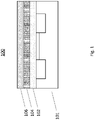
- FIG. 1 is a side view of an exemplary embodiment of an electrical board with a protective coating.
- FIG. 1 a partial view of an exemplary embodiment of a protective coating in accordance with the disclosure is shown in FIG. 1 and is designated generally by reference character 100.
- the protective coatings and methods of making such composite material and electrical conductors described herein can be used for electrical systems and components for aircraft.
- Fig. 1 shows a protective coating system 100, covering an electric circuit board 101 having conductive elements and tracts.
- the system includes a first protective layer 102, a second protective layer 104 covering the first protective layer 102 and a third protective layer 106 covering the second protective layer 104.
- the second protective layer 104 includes Parylene, or can be exclusively Parylene. Parylene acts as a dry film lubricant, eliminating the need for liquid release agents and provides protection from moisture, corrosive bodily fluids, chemicals, gases, temperature and fungus. Parylene is a true conformal coating. It provides pinhole-free, uniform, and controllable thickness, when applied.
- the third protective layer can be silicone based. Silicone top layer maximizes both tracking and ozone resistance of the protective coating 100.
- the first protective layer 102 includes a UV breakable adhesive so that it can be broken and the entire coating system can be removed without having to perform other, possibly hazardous, abrasive, and time-consuming cleaning exercises.
- the third protective layer 106 is a transparent layer and along the second protective layer, 104 can pass UV light of at least 350 nm in order to activate the breakup of the first protective layer 102.
- the method can further include plasma etching the second protective layer 104 in order to solidify it.
- the third protective layer 106 When applying the third protective layer 106, it is cured at approximately 170 degrees Fahrenheit for at least 30 minutes or can also be left at ambient room temperature conditions for an hour. It is also considered that a fourth protective layer, an adhesion promoter, can be placed between the second protective layer 102 and the third protective layer 106.
Landscapes
- Engineering & Computer Science (AREA)
- Microelectronics & Electronic Packaging (AREA)
- Manufacturing & Machinery (AREA)
- Non-Metallic Protective Coatings For Printed Circuits (AREA)
- Laminated Bodies (AREA)
- Application Of Or Painting With Fluid Materials (AREA)
Abstract
Description
- The present disclosure relates generally to a protective coating, and more specifically to three layer conformal coating for electronic components.
- Aircraft commonly employ electrical components for a variety of functions. Today's aircraft rely more and more on electrical components and their reliability. Electrical components are sometimes covered in Parylene in order to protect them from the elements. However, Parylene is known to have issues as well, its composition makes it particularly prone to tracking, which can lead to excessive creepage distance requirements at the combination of high voltage and altitude, which in turn results in larger component size. Moreover, it has poor resistance to ozone, which will also be exacerbated at high voltages and requires abrasion and toxic, and possibly flammable solvents for removal, which creates hazardous conditions during servicing. Although conventional electrical and electromagnetic components have been protected and functioned safely by using conventional methods, there is still a need in the art for improved protective coatings. The present disclosure provides a solution for this need.
- A protective coating system or a protective layer (e.g. for use in an electronic component or formed by a method as described herein) includes a first protective layer, a second protective layer covering at least a portion of the first protective layer, wherein the second protective layer includes Parylene, and a third protective layer covering at least a portion of the second protective layer.
- An electronic component (e.g. one comprising the protective layer or system as described herein, or formed by a method as described herein) is also disclosed. The electronic component comprises a substrate having at least one conductive tract; a first protective layer covering the substrate and the conductive tract; a second protective layer covering at least a portion of the first protective layer, wherein the second protective layer includes Parylene; and a third protective layer covering at least a portion of the second protective layer.
- The third protective layer can be silicone based. The protective coating can be used to cover electric circuit boards and other electronic components having conductive elements and tracts.
- The first protective layer can include a UV breakable adhesive. The third protective layer can be a transparent layer. The third protective layer and/or the second protective layer can transmit UV light at a greater than 350 nm frequency.
- In some embodiments, each of the layers are different.
- In some embodiments, the second protective layer is coated with a fourth protective layer before the third protective layer (e.g. a fourth protective layer is between the second and third protective layers). The fourth protective layer may be or comprise an adhesion promoter.
- A method of applying a protective coating (e.g. a protective coating system or a protective layer as herein described) is also disclosed. The method includes covering at least a portion of the circuit board with a first protective layer, covering at least a portion of the first protective layer with a second protective layer including Parylene, and covering at least a portion the second protective layer with a third protective layer.
- A method of protecting an electronic component (e.g. making an electronic component as herein described, or a method of applying a protective coating system or a protective layer as herein described) is also disclosed. The method comprises covering at least a portion of the electronic component with a first protective layer; covering at least a portion the first protective layer with a second protective layer including Parylene; and covering at least a portion the second protective layer with a third protective layer.
- Each of the layers can be different.
- The third protective layer can be cured, e.g. at 170 degrees Fahrenheit, e.g. for at least 30 minutes. The second protective layer can be coated with a fourth protective layer, e.g. an adhesion promoter, before the third protective layer. The method can further include plasma etching the second protective layer. The plasma etching may take place before coating with the third protective layer.
- The first protective layer can be removed. In some embodiments, the first protective layer can be removed while maintaining the second protective layer and maintaining the third protective layer, e.g. by shining a UV ray at at least 350 nm frequency to degrade the first protective layer.
- These and other features of the systems and methods of the subject disclosure will become more readily apparent to those skilled in the art from the following detailed description of the preferred embodiments taken in conjunction with the drawings.
- So that those skilled in the art to which the subject disclosure appertains will readily understand how to make and use the devices and methods of the subject disclosure without undue experimentation, embodiments thereof will be described in detail herein below with reference to certain figures, wherein:
FIG. 1 is a side view of an exemplary embodiment of an electrical board with a protective coating. - Reference will now be made to the drawings wherein like reference numerals identify similar structural features or aspects of the subject disclosure. For purposes of explanation and illustration, and not limitation, a partial view of an exemplary embodiment of a protective coating in accordance with the disclosure is shown in
FIG. 1 and is designated generally byreference character 100. The protective coatings and methods of making such composite material and electrical conductors described herein can be used for electrical systems and components for aircraft. -
Fig. 1 shows aprotective coating system 100, covering anelectric circuit board 101 having conductive elements and tracts. The system includes a firstprotective layer 102, a secondprotective layer 104 covering the firstprotective layer 102 and a thirdprotective layer 106 covering the secondprotective layer 104. The secondprotective layer 104 includes Parylene, or can be exclusively Parylene. Parylene acts as a dry film lubricant, eliminating the need for liquid release agents and provides protection from moisture, corrosive bodily fluids, chemicals, gases, temperature and fungus. Parylene is a true conformal coating. It provides pinhole-free, uniform, and controllable thickness, when applied. It can be applied at room temperature yet can tolerate long-term, high heat, such as 180F conditions, and penetrates spaces as narrow as 10µm. However, Ozone can reach 500ppbV at cruise conditions and unlike cabin systems, high voltage systems are not protected by ozone converter. In combination with HV fields, ozone will degrade the Parylene coatings well before 30,000 hours. Thus it's necessary to both protect it and easily remove it if it has degraded. The third protective layer can be silicone based. Silicone top layer maximizes both tracking and ozone resistance of theprotective coating 100. - The first
protective layer 102 includes a UV breakable adhesive so that it can be broken and the entire coating system can be removed without having to perform other, possibly hazardous, abrasive, and time-consuming cleaning exercises. The thirdprotective layer 106 is a transparent layer and along the second protective layer, 104 can pass UV light of at least 350 nm in order to activate the breakup of the firstprotective layer 102. - The method can further include plasma etching the second
protective layer 104 in order to solidify it. When applying the thirdprotective layer 106, it is cured at approximately 170 degrees Fahrenheit for at least 30 minutes or can also be left at ambient room temperature conditions for an hour. It is also considered that a fourth protective layer, an adhesion promoter, can be placed between the secondprotective layer 102 and the thirdprotective layer 106. - Certain embodiments of the present disclosure are as follows:
- 1. An electronic component comprising:
- a substrate having at least one conductive tract;
- a first protective layer covering the substrate and the conductive tract;
- a second protective layer covering at least a portion of the first protective layer, wherein
- the second protective layer includes Parylene; and
- a third protective layer covering at least a portion of the second protective layer.
- 2. The electronic component of embodiment 1, wherein the first protective layer includes a UV breakable adhesive.
- 3. The electronic component of embodiment 1, wherein the third protective layer is a transparent layer.
- 4. The electronic component of embodiment 1, wherein the third protective layer is silicone based.
- 5. The electronic component of embodiment 1, wherein the third protective layer can transmit UV light at a greater than 350 nm frequency.
- 6. The electronic component of embodiment 1, wherein the second protective layer can transmit UV light at a greater than 350 nm frequency.
- 7. A method of protecting an electronic component comprising:
- covering at least a portion of the electronic component with a first protective layer;
- covering at least a portion the first protective layer with a second protective layer including Parylene; and
- covering at least a portion the second protective layer with a third protective layer.
- 8. The method of embodiment 7, wherein each of the layers are different.
- 9. The method of embodiment 7, further comprising curing the third protective layer.
- 10. The method of embodiment 12, wherein a curing temperature is at least 170 degrees Fahrenheit.
- 11. The method of embodiment 12, wherein a curing time is at least 30 minutes.
- 12. The method of embodiment 7, further comprising coating the second protective layer with a fourth protective layer before the third protective layer.
- 13. The method of embodiment 15, wherein the fourth protective layer is an adhesion promoter.
- 14. The method of embodiment 7, further comprising plasma etching the second protective layer.
- 15. The method of embodiment 17, wherein the plasma etching take place before coating with the third protective layer.
- 16. The method of embodiment 7, further comprising removing the first protective layer.
- 17. The method of embodiment 9, wherein the first layer is removed while maintaining the second protective layer and maintaining the third protective layer.
- 18. The method of embodiment 9, further comprising shining a UV ray at at least 350 nm frequency to degrade the first protective layer.
- 19. A protective layer comprising:
- a first protective layer;
- a second protective layer covering at least a portion of the first protective layer, wherein
- the second protective layer includes Parylene; and
- a third protective layer covering at least a portion of the second protective layer.
- 20. The protective layer of claim 19, wherein the third protective layer is silicone based.
- The methods and systems of the present disclosure, as described above and shown in the drawings, provide for a coating having superior protection and cleaning properties. The coating and methods of the subject disclosure have been shown and described with reference to preferred embodiments, those skilled in the art will readily appreciate that changes and/or modifications may be made thereto without departing from the scope of the subject disclosure.
Claims (15)
- An electronic component comprising:a substrate having at least one conductive tract;a first protective layer covering the substrate and the conductive tract;a second protective layer covering at least a portion of the first protective layer, wherein the second protective layer includes Parylene; anda third protective layer covering at least a portion of the second protective layer.
- The electronic component of claim 1, wherein the first protective layer includes a UV breakable adhesive and/or wherein each of the layers are different.
- The electronic component of claim 1 or claim 2, wherein the third protective layer is a transparent layer.
- The electronic component of any preceding claim, wherein the third protective layer is silicone based.
- The electronic component of any preceding claim, wherein the third protective layer can transmit UV light at a greater than 350 nm frequency and/or wherein the second protective layer can transmit UV light at a greater than 350 nm frequency.
- A method of protecting an electronic component comprising:covering at least a portion of the electronic component with a first protective layer;covering at least a portion the first protective layer with a second protective layer including Parylene; andcovering at least a portion the second protective layer with a third protective layer.
- The method of claim 6, wherein each of the layers are different.
- The method of claim 6 or claim 7, further comprising curing the third protective layer, e.g. wherein a curing temperature is at least 170 degrees Fahrenheit and/or wherein a curing time is at least 30 minutes.
- The method of any one of claims 6-8, further comprising coating the second protective layer with a fourth protective layer before the third protective layer.
- The method of claim 9, wherein the fourth protective layer is an adhesion promoter.
- The method of any one of claims 6-10, further comprising plasma etching the second protective layer.
- The method of claim 11, wherein the plasma etching takes place before coating with the third protective layer.
- The method of any one of claims 6-12, further comprising removing the first protective layer, e.g. wherein the first layer is removed while maintaining the second protective layer and maintaining the third protective layer.
- The method of any one of claims 6-13, further comprising shining a UV ray at at least 350 nm frequency to degrade the first protective layer.
- A protective layer comprising:a first protective layer;a second protective layer covering at least a portion of the first protective layer, wherein the second protective layer includes Parylene; anda third protective layer covering at least a portion of the second protective layer,optionally wherein the third protective layer is silicone based.
Applications Claiming Priority (1)
| Application Number | Priority Date | Filing Date | Title |
|---|---|---|---|
| US17/131,726 US11589464B2 (en) | 2020-12-22 | 2020-12-22 | Protective coating for electrical components and method of making the protective coating |
Publications (1)
| Publication Number | Publication Date |
|---|---|
| EP4021152A1 true EP4021152A1 (en) | 2022-06-29 |
Family
ID=79317169
Family Applications (1)
| Application Number | Title | Priority Date | Filing Date |
|---|---|---|---|
| EP21215604.6A Pending EP4021152A1 (en) | 2020-12-22 | 2021-12-17 | A protective coating for electrical components and method of making the protective coating |
Country Status (2)
| Country | Link |
|---|---|
| US (1) | US11589464B2 (en) |
| EP (1) | EP4021152A1 (en) |
Citations (3)
| Publication number | Priority date | Publication date | Assignee | Title |
|---|---|---|---|---|
| US20160262261A1 (en) * | 2015-03-02 | 2016-09-08 | Apple Inc. | Printed Circuits With Laser Ablated Conformal Coating Openings |
| US20170246847A1 (en) * | 2014-09-16 | 2017-08-31 | Smilesonica Inc. | Silicone and polymer substrate composite materials, methods, and uses of the same |
| US20190106547A1 (en) * | 2017-10-11 | 2019-04-11 | Taimide Tech. Inc. | Transparent polyimide composite film for flexible display and method for manufacturing the same |
Family Cites Families (32)
| Publication number | Priority date | Publication date | Assignee | Title |
|---|---|---|---|---|
| US4979803A (en) * | 1989-02-02 | 1990-12-25 | Eastman Kodak Company | Color filter array for area image sensors |
| DE69029503T2 (en) * | 1989-10-13 | 1997-05-22 | Toshiba Kawasaki Kk | Aperture pattern planographic printing plate for producing a shadow mask and method for producing this mask |
| US5654084A (en) * | 1994-07-22 | 1997-08-05 | Martin Marietta Energy Systems, Inc. | Protective coatings for sensitive materials |
| JPH1026761A (en) * | 1996-07-10 | 1998-01-27 | Sharp Corp | Method and apparatus for aligning liquid crystal and liquid crystal display element |
| US6391220B1 (en) * | 1999-08-18 | 2002-05-21 | Fujitsu Limited, Inc. | Methods for fabricating flexible circuit structures |
| DE19953655A1 (en) * | 1999-11-08 | 2001-05-10 | Basf Ag | Goniochromatic gloss pigments based on heated, titanium dioxide-coated silicate flakes in a reducing atmosphere |
| US6334761B1 (en) * | 2000-03-02 | 2002-01-01 | California Institute Of Technology | Check-valved silicon diaphragm pump and method of fabricating the same |
| US20010052752A1 (en) * | 2000-04-25 | 2001-12-20 | Ghosh Amalkumar P. | Thin film encapsulation of organic light emitting diode devices |
| US20020086188A1 (en) * | 2000-10-12 | 2002-07-04 | Eugene Halsey | Reduced contrast improved transmission conductively coated transparent substrate |
| WO2003013199A2 (en) | 2001-07-27 | 2003-02-13 | Eikos, Inc. | Conformal coatings comprising carbon nanotubes |
| US6737753B2 (en) | 2001-09-28 | 2004-05-18 | Osram Opto Semiconductor Gmbh | Barrier stack |
| EP1438750A1 (en) * | 2001-10-26 | 2004-07-21 | STMicroelectronics N.V. | Method for producing a tfa image sensor and one such tfa image sensor |
| JP4026745B2 (en) * | 2002-03-26 | 2007-12-26 | 財団法人大阪産業振興機構 | Medical system and manufacturing method thereof |
| JP4223247B2 (en) * | 2002-08-12 | 2009-02-12 | シャープ株式会社 | Organic insulating film manufacturing method and inkjet head |
| US20050112650A1 (en) * | 2003-10-20 | 2005-05-26 | Ciphergen Biosystems, Inc. | Reactive polyurethane-based polymers |
| US6958531B2 (en) * | 2003-11-14 | 2005-10-25 | The Regents Of The University Of Michigan | Multi-substrate package and method for assembling same |
| WO2005114720A2 (en) * | 2004-05-14 | 2005-12-01 | California Institute Of Technology | Parylene-based flexible multi-electrode arrays for neuronal stimulation and recording and methods for manufacturing the same |
| EP2319558B1 (en) * | 2006-03-14 | 2014-05-21 | University Of Southern California | Mems device for delivery of therapeutic agents |
| US20160000602A1 (en) * | 2006-03-14 | 2016-01-07 | Ellis Meng | Mems device and method for delivery of therapeutic agents |
| US7767589B2 (en) * | 2007-02-07 | 2010-08-03 | Raytheon Company | Passivation layer for a circuit device and method of manufacture |
| US8173906B2 (en) * | 2007-02-07 | 2012-05-08 | Raytheon Company | Environmental protection coating system and method |
| EP2666510B1 (en) * | 2007-12-20 | 2017-10-18 | University Of Southern California | Apparatus for controlled delivery of therapeutic agents |
| AU2009234506B2 (en) | 2008-04-09 | 2013-11-21 | Agency For Science, Technology And Research | Multilayer film for encapsulating oxygen and/or moisture sensitive electronic devices |
| US7988778B2 (en) * | 2008-12-16 | 2011-08-02 | Cheng Uei Precision Industry Co., Ltd. | Method of making composite coating and product formed with the composite coating |
| TWI377646B (en) | 2009-08-03 | 2012-11-21 | Substrate structures applied in flexible electrical devices and fabrication method thereof | |
| US20140183669A1 (en) * | 2010-03-26 | 2014-07-03 | Wayne State University | Resonant sensor with asymmetric gapped cantilevers |
| US20130248712A1 (en) * | 2010-12-13 | 2013-09-26 | Reza Abdolvand | Nanowire thermoelectric infrared detector |
| JP5744570B2 (en) * | 2011-03-02 | 2015-07-08 | キヤノン株式会社 | Radiation detection apparatus, method for manufacturing radiation detection apparatus, and radiation detection system |
| WO2013109749A1 (en) * | 2012-01-17 | 2013-07-25 | The Penn State Research Foundation | Flexible filter device for capturing of particles or cells in a fluid |
| US10736537B2 (en) * | 2015-10-12 | 2020-08-11 | California Institute Of Technology | Electrical impedance spectroscopy measurement based on concentric bipolar microelectrode sensor |
| TW201916386A (en) * | 2017-10-13 | 2019-04-16 | 國立臺灣大學 | Microfluidic chip and manufacturing method thereof and integrated microfluidic chip system |
| US20200319135A1 (en) * | 2018-04-26 | 2020-10-08 | Shih-Kang Fan | Microfluidic chip and manufacturing method thereof and integrated microfluidic chip system |
-
2020
- 2020-12-22 US US17/131,726 patent/US11589464B2/en active Active
-
2021
- 2021-12-17 EP EP21215604.6A patent/EP4021152A1/en active Pending
Patent Citations (3)
| Publication number | Priority date | Publication date | Assignee | Title |
|---|---|---|---|---|
| US20170246847A1 (en) * | 2014-09-16 | 2017-08-31 | Smilesonica Inc. | Silicone and polymer substrate composite materials, methods, and uses of the same |
| US20160262261A1 (en) * | 2015-03-02 | 2016-09-08 | Apple Inc. | Printed Circuits With Laser Ablated Conformal Coating Openings |
| US20190106547A1 (en) * | 2017-10-11 | 2019-04-11 | Taimide Tech. Inc. | Transparent polyimide composite film for flexible display and method for manufacturing the same |
Also Published As
| Publication number | Publication date |
|---|---|
| US11589464B2 (en) | 2023-02-21 |
| US20220201869A1 (en) | 2022-06-23 |
Similar Documents
| Publication | Publication Date | Title |
|---|---|---|
| US7214889B2 (en) | Board-level conformal EMI shield having an electrically-conductive polymer coating over a thermally-conductive dielectric coating | |
| Licari | Coating materials for electronic applications: polymers, processing, reliability, testing | |
| US7109817B2 (en) | Interference signal decoupling on a printed circuit board | |
| CN107409483B (en) | Electromagnetic wave shielding sheet, electromagnetic wave shielding wired circuit board, and electronic apparatus | |
| US20050095410A1 (en) | Board-level conformal EMI shield having an electrically-conductive polymer coating over a thermally-conductive dielectric coating | |
| KR101139545B1 (en) | Cover tape for packaging electronic part and electronic part package | |
| KR20010071409A (en) | Rigid/flex printed circuit board and manufacturing method therefor | |
| US6261680B1 (en) | Electronic assembly with charge-dissipating transparent conformal coating | |
| US7008483B2 (en) | Curing printed circuit board coatings | |
| EP0749500B1 (en) | Method of manufacturing a thin silicon-oxide layer | |
| KR101832736B1 (en) | EMI shielding films and methods of manufacturing the same | |
| US6316104B1 (en) | Adhesives and circuit materials using said adhesives | |
| TW201442864A (en) | Electromagnetic wave shielding film and method of preparing same | |
| US11589464B2 (en) | Protective coating for electrical components and method of making the protective coating | |
| CN106042519B (en) | Conductive adhesive sheet for FPC and FPC using the same | |
| KR100791557B1 (en) | Plastic-metal thin film and its manufacturing method | |
| US10182497B1 (en) | Transparent and antistatic conformal coating for internal ESD mitigation in space environment | |
| JP4195365B2 (en) | Circuit board with flame resistance and moisture resistance | |
| CN115024029A (en) | Electromagnetic wave shielding film | |
| WO2016117719A1 (en) | Electromagnetic wave shielding film and manufacturing method thereof | |
| WO2016196953A1 (en) | Process for protecting an electronic device with a hydrophobic coating | |
| JP4437639B2 (en) | Flat cable manufacturing method | |
| JP3857254B2 (en) | Holding and conveying jig | |
| US20080236883A1 (en) | Structures for implementing emi shielding for rigid cards and flexible circuits | |
| US20220022324A1 (en) | Method for manufacturing water resistant printed circuit board |
Legal Events
| Date | Code | Title | Description |
|---|---|---|---|
| PUAI | Public reference made under article 153(3) epc to a published international application that has entered the european phase |
Free format text: ORIGINAL CODE: 0009012 |
|
| STAA | Information on the status of an ep patent application or granted ep patent |
Free format text: STATUS: THE APPLICATION HAS BEEN PUBLISHED |
|
| AK | Designated contracting states |
Kind code of ref document: A1 Designated state(s): AL AT BE BG CH CY CZ DE DK EE ES FI FR GB GR HR HU IE IS IT LI LT LU LV MC MK MT NL NO PL PT RO RS SE SI SK SM TR |
|
| STAA | Information on the status of an ep patent application or granted ep patent |
Free format text: STATUS: REQUEST FOR EXAMINATION WAS MADE |
|
| 17P | Request for examination filed |
Effective date: 20221223 |
|
| RBV | Designated contracting states (corrected) |
Designated state(s): AL AT BE BG CH CY CZ DE DK EE ES FI FR GB GR HR HU IE IS IT LI LT LU LV MC MK MT NL NO PL PT RO RS SE SI SK SM TR |
|
| GRAP | Despatch of communication of intention to grant a patent |
Free format text: ORIGINAL CODE: EPIDOSNIGR1 |
|
| STAA | Information on the status of an ep patent application or granted ep patent |
Free format text: STATUS: GRANT OF PATENT IS INTENDED |
|
| INTG | Intention to grant announced |
Effective date: 20251203 |
|
| GRAJ | Information related to disapproval of communication of intention to grant by the applicant or resumption of examination proceedings by the epo deleted |
Free format text: ORIGINAL CODE: EPIDOSDIGR1 |
|
| STAA | Information on the status of an ep patent application or granted ep patent |
Free format text: STATUS: REQUEST FOR EXAMINATION WAS MADE |
|
| GRAP | Despatch of communication of intention to grant a patent |
Free format text: ORIGINAL CODE: EPIDOSNIGR1 |
|
| STAA | Information on the status of an ep patent application or granted ep patent |
Free format text: STATUS: GRANT OF PATENT IS INTENDED |
|
| INTC | Intention to grant announced (deleted) |