EP4020733B1 - Modular surge protector - Google Patents
Modular surge protector Download PDFInfo
- Publication number
- EP4020733B1 EP4020733B1 EP20906922.8A EP20906922A EP4020733B1 EP 4020733 B1 EP4020733 B1 EP 4020733B1 EP 20906922 A EP20906922 A EP 20906922A EP 4020733 B1 EP4020733 B1 EP 4020733B1
- Authority
- EP
- European Patent Office
- Prior art keywords
- varistor
- electrode
- discharge tube
- unit
- frame
- Prior art date
- Legal status (The legal status is an assumption and is not a legal conclusion. Google has not performed a legal analysis and makes no representation as to the accuracy of the status listed.)
- Active
Links
Images


Classifications
-
- H—ELECTRICITY
- H01—ELECTRIC ELEMENTS
- H01T—SPARK GAPS; OVERVOLTAGE ARRESTERS USING SPARK GAPS; SPARKING PLUGS; CORONA DEVICES; GENERATING IONS TO BE INTRODUCED INTO NON-ENCLOSED GASES
- H01T1/00—Details of spark gaps
- H01T1/14—Means structurally associated with spark gap for protecting it against overload or for disconnecting it in case of failure
-
- H—ELECTRICITY
- H01—ELECTRIC ELEMENTS
- H01C—RESISTORS
- H01C7/00—Non-adjustable resistors formed as one or more layers or coatings; Non-adjustable resistors made from powdered conducting material or powdered semi-conducting material with or without insulating material
- H01C7/10—Non-adjustable resistors formed as one or more layers or coatings; Non-adjustable resistors made from powdered conducting material or powdered semi-conducting material with or without insulating material voltage responsive, i.e. varistors
- H01C7/12—Overvoltage protection resistors
- H01C7/126—Means for protecting against excessive pressure or for disconnecting in case of failure
-
- H—ELECTRICITY
- H01—ELECTRIC ELEMENTS
- H01T—SPARK GAPS; OVERVOLTAGE ARRESTERS USING SPARK GAPS; SPARKING PLUGS; CORONA DEVICES; GENERATING IONS TO BE INTRODUCED INTO NON-ENCLOSED GASES
- H01T4/00—Overvoltage arresters using spark gaps
- H01T4/06—Mounting arrangements for a plurality of overvoltage arresters
-
- H—ELECTRICITY
- H02—GENERATION; CONVERSION OR DISTRIBUTION OF ELECTRIC POWER
- H02H—EMERGENCY PROTECTIVE CIRCUIT ARRANGEMENTS
- H02H3/00—Emergency protective circuit arrangements for automatic disconnection directly responsive to an undesired change from normal electric working condition with or without subsequent reconnection ; integrated protection
- H02H3/02—Details
- H02H3/025—Disconnection after limiting, e.g. when limiting is not sufficient or for facilitating disconnection
-
- H—ELECTRICITY
- H02—GENERATION; CONVERSION OR DISTRIBUTION OF ELECTRIC POWER
- H02H—EMERGENCY PROTECTIVE CIRCUIT ARRANGEMENTS
- H02H9/00—Emergency protective circuit arrangements for limiting excess current or voltage without disconnection
- H02H9/04—Emergency protective circuit arrangements for limiting excess current or voltage without disconnection responsive to excess voltage
- H02H9/06—Emergency protective circuit arrangements for limiting excess current or voltage without disconnection responsive to excess voltage using spark-gap arresters
Definitions
- the present invention provides a modular surge protector, and belongs to the technical field of lightning protection in the international patent classification (IPC).
- IPC international patent classification
- a surge protector is an electronic apparatus that provides safety protection for various electronic devices, instruments, and communication lines. It is intended to protect current or voltage spikes generated in electrical circuits or communication lines due to external interferences.
- US 2019/295792 A1 discloses an overvoltage protection arrangement having: a plurality of planar varistors, which are arranged on a first side of a supporting plate; at least one gas arrester; and at least one thermal disconnection device, which is in close thermal contact with at least one of the varistors.
- the aforementioned components are surrounded by an outer housing, and electrical connection means for soldering to a printed circuit board are also provided on the second side of the supporting plate.
- the varistors have a parallel stack arrangement, which is delimited on each of two opposing sides by an insulating partition wall which can be attached to the supporting plate.
- Each partition wall has at least one opening for a varistor terminal, each varistor terminal being connected to a thermal disconnection device, which in turn comprises a spring-loaded disconnecting lever, the respective disconnecting lever being connected at its first end to the respective varistor terminal by a soldered connection and wherein its second end merges into one of the electrical terminals and penetrates through the supporting plate.
- the thermal disconnection device also has an insulating slide, whose free end acts on the disconnecting lever, wherein the slide runs in recesses in the respective partition wall, and a change in the position of the slide can be seen by means of a viewing opening in the outer housing.
- WO 2019/205863 A1 discloses a surge protector module, comprising line varistors connected in series and a heat detaching unit.
- the heat detaching unit comprises elastic members, insulating members, alloys having a low melting point, a connecting member, and leads disposed on the connecting member.
- the insulating members have an opening.
- the elastic members are disposed in the openings, and the elastic members have a hollow passage.
- the leads pass through the passages and are connected to the lead varistors via the alloys having a low melting point.
- the elastic members abut the insulating members at one end, abut the connecting member at another end, and are in a compressed state.
- the insulating members abut the alloys having a low melting point under a rebound force of the elastic members.
- a plurality of surge protection devices generate heat and transfer the heat to a detaching solder joint, such that the alloys having a low melting point are disconnected early when a fault occurs in a surge protection device.
- CN209675934 U discloses a surge protector.
- the device comprises a shell, and a first assembly and a second assembly which are arranged in the shell, the first assembly and the second assembly are both of a flat structure.
- the first assembly comprises a first frame, a first piezoresistor and a first thermal tripping device, the first piezoresistor and the first thermal tripping device are arranged on the two sides of the first frame respectively
- the second assembly comprises a second frame, a second piezoresistor and a second thermal tripping device, the second piezoresistor and the second thermal tripping device are arranged on the two sides of the second frame respectively
- the discharge tube set is arranged on the second frame and arranged on the same side as the second thermal tripping device.
- the first frame and the second frame are arranged in a stacked mode, the first piezoresistor and the second piezoresistor are connected back to back, and a third pin electrode is led out through the discharge tube set.
- an objective of the present invention is to provide a modular surge protector, which yields a compact structure and a small size through the modular design.
- a modular surge protector includes a shell, a discharge tube unit, a first varistor unit and a second varistor unit, where the discharge tube unit, the first varistor unit and the second varistor unit are arranged in the shell.
- the first varistor unit and the second varistor unit are stacked, the discharge tube unit is provided at a same side of each of the first varistor unit and the second varistor unit, a first electrode is led out from the first varistor unit, a second electrode is led out from the second varistor unit, and a third electrode is led out from the discharge tube unit.
- the discharge tube unit includes a discharge tube frame; a first slot, a second slot and a third slot are formed in the discharge tube frame, the first slot and the second slot are provided side by side at a side of the discharge tube frame and respectively configured to accommodate the first discharge tube and the second discharge tube; the third slot are provided at a side of the discharge tube frame and cooperate with an end portion of each of the first varistor unit and the second varistor unit; the first varistor unit and the second varistor unit may be horizontally stacked; and the first discharge tube and the second discharge tube may be vertically provided.
- the discharge tube unit may include a first discharge tube and a second discharge tube
- the first varistor unit may include a first varistor
- the first electrode may be led out from a positive electrode of the first varistor
- the second varistor unit may include a second varistor
- the second electrode may be led out from a positive electrode of the second varistor
- the first varistor unit may include a first frame and a first thermal trip, the first thermal trip and the first varistor may be respectively arranged at two sides of the first frame, and the first electrode may be led out from the positive electrode of the first varistor through the first thermal trip;
- first varistor unit and the second varistor unit may be clamped by a clamping member.
- each of the first thermal trip and the second thermal trip may include a spring electrode, a sliding member and a compression spring
- the spring electrode may be connected to a positive electrode of a corresponding varistor through a fusible alloy, and the spring electrode may abut against the sliding member and keep the compression spring in a compressed state; and in a failure state, the fusible alloy may be molten, the sliding member may slide along a guide track on the first frame or the second frame under an action of the compression spring such that the spring electrode may be isolated from the positive electrode of the corresponding varistor, and a side of the sliding member may extend outward to form an indication portion.
- the shell may include a shell body and an engageable cover plate, and the first electrode, the second electrode and the third electrode may be led out from a side of a cover plate to form a welding plate structure.
- Three frames are provided for the discharge tubes and the varistors to form the modular design.
- the present invention has the reasonable arrangement and compact structure, and meets the requirements of miniaturization applications.
- a modular surge protector includes a shell 1, a discharge tube unit 2, a first varistor unit 3 and a second varistor unit 4, where the discharge tube unit 2, the first varistor unit 3 and the second varistor unit 4 are arranged in the shell 1.
- the first varistor unit 3 and the second varistor unit 4 are stacked.
- the discharge tube unit 2 is provided at a same side of each of the first varistor unit 3 and the second varistor unit 4.
- a first electrode 101 is led out from the first varistor unit 3.
- a second electrode 102 is led out from the second varistor unit 4.
- a third electrode 103 is led out from the discharge tube unit 2.
- the shell 1 includes a shell body 11 and an engageable cover plate 12.
- the first electrode 101, the second electrode 102 and the third electrode 103 are led out from a side of a cover plate 12 to form a welding plate structure.
- the first electrode is a phase electrode L, namely a live electrode.
- the second electrode is a grounding electrode PE.
- the third electrode is a neutral electrode N.
- Two indication windows 104 cooperated with an indication portion of an internal sliding member are formed in the shell body 11. Once tripped, the surge protector can give an indication with a corresponding color. Specifically, it turns green normally and turns red once tripped.
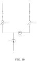
- the protective circuit includes three modules that are respectively arranged in the discharge tube unit 2, the first varistor unit 3 and the second varistor unit 4.
- the discharge tube unit includes a first discharge tube GDT1 and a second discharge tube GDT2.
- the first varistor unit includes a first varistor MOV1.
- the second varistor unit includes a second varistor MOV2.
- the surge protector includes a series circuit for the phase electrode L, the first varistor MOV1, the first discharge tube GDT1 and the neutral electrode N, a series circuit for the first varistor MOV1, the second discharge tube GDT2, the second varistor MOV2 and the grounding electrode PE, and a series circuit for the neutral electrode N, the first discharge tube GDT1, the second discharge tube GDT2, the second varistor MOV2 and the grounding electrode PE.
- the discharge tube unit 2 in the embodiment includes a first discharge tube 21 and a second discharge tube 22.
- the first varistor unit 3 includes a first varistor 31.
- the first electrode 101 is led out from a positive electrode of the first varistor 31.
- the second varistor unit 4 includes a second varistor 41.
- the second electrode 102 is led out from a positive electrode of the second varistor 41.
- the first discharge tube 21 and the second discharge tube 22 are diode discharge tubes and connected through a discharge tube common electrode.
- the discharge tube common electrode is electrically connected to a back electrode of the first varistor 31, a back electrode of the second varistor 41 is connected to a back electrode of the second discharge tube 22, and the third electrode 103 is led out from the first discharge tube 21.
- the first varistor unit 3 further includes a first frame 32 and a first thermal trip 33.
- the first thermal trip 33 and the first varistor 31 are respectively arranged at two sides of the first frame 32.
- the first electrode 101 is led out from the positive electrode of the first varistor 31 through the first thermal trip 33.
- the first thermal trip 33 includes a spring electrode 331, a sliding member 332 and a compression spring 333.
- the spring electrode 331 and the positive electrode 311 of the first varistor 31 are connected at an opening 322 through a fusible alloy.
- the spring electrode 331 abuts against the sliding member 332 and keeps the compression spring 333 in a compressed state.
- the fusible alloy is molten
- the sliding member 332 slides along a guide track 321 on the first frame 32 under an action of the compression spring 333 such that the spring electrode is isolated from the positive electrode of the corresponding varistor, and a side of the sliding member 332 extends outward to form an indication portion 3320.
- the spring electrode 331 extends outward to form a pin electrode, namely the first electrode.
- the first varistor and the second varistor are arranged between the first frame and a second frame.
- a clapboard 5 is provided between the first varistor and the second varistor.
- the back electrode of the first varistor 31 is led out from a sidewall of the frame to form a welding point 312.
- the second varistor unit 4 further includes a second frame 42 and a second thermal trip 43.
- the second thermal trip 43 and the second varistor 41 are respectively arranged at two sides of the second frame 42.
- the second electrode is led out from the positive electrode of the second varistor 41 through the second thermal trip 43.
- the second thermal trip 43 includes a spring electrode 431, a sliding member 432 and a compression spring 433.
- the spring electrode 431 and the positive electrode 411 of the second varistor 41 are connected at an opening 422 through a fusible alloy.
- the spring electrode 431 abuts against the sliding member 432 and keeps the compression spring 433 in a compressed state.
- the fusible alloy is molten
- the sliding member 432 slides along a guide track 421 on the second frame 42 under an action of the compression spring such that the spring electrode 431 is isolated from the positive electrode of the varistor, and a side of the sliding member is formed into an indication portion 4320.
- the spring electrode 431 is led out through the second electrode 102.
- the back electrode of the second varistor 41 is led out from a sidewall of the frame to form a welding point 412.
- the discharge tube unit 2 in the embodiment further includes a discharge tube frame 23.
- a first slot, a second slot and a third slot 231 are formed in the discharge tube frame 23.
- the first slot and the second slot are provided side by side at a side of the discharge tube frame and respectively configured to accommodate the first discharge tube 21 and the second discharge tube 22.
- the third slot 231 is provided at a side of the discharge tube frame and cooperates with an end portion of each of the first varistor unit 3 and the second varistor unit 4.
- the first varistor unit 3 and the second varistor unit 4 are horizontally stacked.
- the first discharge tube 21 and the second discharge tube 22 are vertically provided.
- the apparatus embodiment described above is merely schematic, where the unit described as a separate component may or may not be physically separated, and a component displayed as a unit may or may not be a physical unit, that is, the component may be located at one place, or distributed on multiple network units. Some or all of the modules may be selected based on actual needs to achieve the objectives of the solutions of the embodiments. The person of ordinary skill in the art can understand and implement the embodiments without creative efforts.
- any reference sign between brackets should not be constructed as a limitation on the claims.
- the word “include” does not exclude the presence of elements or steps not listed in the claims.
- the word “one” or “a/an” preceding an element does not exclude the existence of multiple such elements.
- the present invention can be implemented with the assistance of hardware including several different components and the assistance of a properly programmed computer.
- several apparatuses may be embodied by the same hardware item.
- the use of words such as first, second, and third do not indicate any order. The words may be interpreted as names.
Landscapes
- Engineering & Computer Science (AREA)
- Microelectronics & Electronic Packaging (AREA)
- Physics & Mathematics (AREA)
- Electromagnetism (AREA)
- Emergency Protection Circuit Devices (AREA)
- Thermistors And Varistors (AREA)
Description
- The present invention provides a modular surge protector, and belongs to the technical field of lightning protection in the international patent classification (IPC).
- A surge protector is an electronic apparatus that provides safety protection for various electronic devices, instruments, and communication lines. It is intended to protect current or voltage spikes generated in electrical circuits or communication lines due to external interferences.
- Because of restrictions of electronic components and so on, existing modular surge protectors are far from satisfactory to constant miniaturization of electronic products. Therefore, size optimization, reasonable spatial arrangement, greater ease of production and assembly, and higher reliability of the surge protector are problems of concern to a person skilled in the art.
US 2019/295792 A1 discloses an overvoltage protection arrangement having: a plurality of planar varistors, which are arranged on a first side of a supporting plate; at least one gas arrester; and at least one thermal disconnection device, which is in close thermal contact with at least one of the varistors. The aforementioned components are surrounded by an outer housing, and electrical connection means for soldering to a printed circuit board are also provided on the second side of the supporting plate. The varistors have a parallel stack arrangement, which is delimited on each of two opposing sides by an insulating partition wall which can be attached to the supporting plate. Each partition wall has at least one opening for a varistor terminal, each varistor terminal being connected to a thermal disconnection device, which in turn comprises a spring-loaded disconnecting lever, the respective disconnecting lever being connected at its first end to the respective varistor terminal by a soldered connection and wherein its second end merges into one of the electrical terminals and penetrates through the supporting plate. The thermal disconnection device also has an insulating slide, whose free end acts on the disconnecting lever, wherein the slide runs in recesses in the respective partition wall, and a change in the position of the slide can be seen by means of a viewing opening in the outer housing.WO 2019/205863 A1 discloses a surge protector module, comprising line varistors connected in series and a heat detaching unit. The heat detaching unit comprises elastic members, insulating members, alloys having a low melting point, a connecting member, and leads disposed on the connecting member. The insulating members have an opening. The elastic members are disposed in the openings, and the elastic members have a hollow passage. The leads pass through the passages and are connected to the lead varistors via the alloys having a low melting point. The elastic members abut the insulating members at one end, abut the connecting member at another end, and are in a compressed state. The insulating members abut the alloys having a low melting point under a rebound force of the elastic members. A plurality of surge protection devices generate heat and transfer the heat to a detaching solder joint, such that the alloys having a low melting point are disconnected early when a fault occurs in a surge protection device.CN209675934 U discloses a surge protector. The device comprises a shell, and a first assembly and a second assembly which are arranged in the shell, the first assembly and the second assembly are both of a flat structure. The first assembly comprises a first frame, a first piezoresistor and a first thermal tripping device, the first piezoresistor and the first thermal tripping device are arranged on the two sides of the first frame respectively, the second assembly comprises a second frame, a second piezoresistor and a second thermal tripping device, the second piezoresistor and the second thermal tripping device are arranged on the two sides of the second frame respectively, and the discharge tube set is arranged on the second frame and arranged on the same side as the second thermal tripping device. The first frame and the second frame are arranged in a stacked mode, the first piezoresistor and the second piezoresistor are connected back to back, and a third pin electrode is led out through the discharge tube set. - In view of the defects in the prior art, an objective of the present invention is to provide a modular surge protector, which yields a compact structure and a small size through the modular design.
- In order to achieve the above objective, the present invention employs the following technical solutions:
A modular surge protector includes a shell, a discharge tube unit, a first varistor unit and a second varistor unit, where the discharge tube unit, the first varistor unit and the second varistor unit are arranged in the shell. The first varistor unit and the second varistor unit are stacked, the discharge tube unit is provided at a same side of each of the first varistor unit and the second varistor unit, a first electrode is led out from the first varistor unit, a second electrode is led out from the second varistor unit, and a third electrode is led out from the discharge tube unit. The discharge tube unit includes a discharge tube frame; a first slot, a second slot and a third slot are formed in the discharge tube frame, the first slot and the second slot are provided side by side at a side of the discharge tube frame and respectively configured to accommodate the first discharge tube and the second discharge tube; the third slot are provided at a side of the discharge tube frame and cooperate with an end portion of each of the first varistor unit and the second varistor unit; the first varistor unit and the second varistor unit may be horizontally stacked; and the first discharge tube and the second discharge tube may be vertically provided. - Further, the discharge tube unit may include a first discharge tube and a second discharge tube, the first varistor unit may include a first varistor, the first electrode may be led out from a positive electrode of the first varistor, the second varistor unit may include a second varistor, and the second electrode may be led out from a positive electrode of the second varistor;
- the first discharge tube and the second discharge tube may be connected through a discharge tube common electrode, the discharge tube common electrode may be electrically connected to a back electrode of the first varistor, a back electrode of the second varistor may be connected to a back electrode of the second discharge tube, and the third electrode may be led out from the first discharge tube; and
- the first electrode may be a phase electrode, the second electrode may be a grounding electrode, and the third electrode may be a neutral electrode.
- Further, the first varistor unit may include a first frame and a first thermal trip, the first thermal trip and the first varistor may be respectively arranged at two sides of the first frame, and the first electrode may be led out from the positive electrode of the first varistor through the first thermal trip;
- the second varistor unit may include a second frame and a second thermal trip, the second thermal trip and the second varistor may be respectively arranged at two sides of the second frame, and the second electrode may be led out from the positive electrode of the second varistor through the second thermal trip; and
- the first varistor and the second varistor are arranged between the first frame and the second frame.
- Further, the first varistor unit and the second varistor unit may be clamped by a clamping member.
- Further, each of the first thermal trip and the second thermal trip may include a spring electrode, a sliding member and a compression spring, the spring electrode may be connected to a positive electrode of a corresponding varistor through a fusible alloy, and the spring electrode may abut against the sliding member and keep the compression spring in a compressed state; and in a failure state, the fusible alloy may be molten, the sliding member may slide along a guide track on the first frame or the second frame under an action of the compression spring such that the spring electrode may be isolated from the positive electrode of the corresponding varistor, and a side of the sliding member may extend outward to form an indication portion.
- Further, the shell may include a shell body and an engageable cover plate, and the first electrode, the second electrode and the third electrode may be led out from a side of a cover plate to form a welding plate structure.
- Three frames are provided for the discharge tubes and the varistors to form the modular design. With the vertical discharge tubes and the horizontal varistors, the present invention has the reasonable arrangement and compact structure, and meets the requirements of miniaturization applications.
- The above description is merely a summary of the technical solutions of the present invention. In order to make the technical means of the present invention understood more clearly and implemented in accordance with the content of the specification, and in order to make the above and other objectives, features and advantages of the present invention more obvious and comprehensible, specific implementations of the present invention are described below.
- To describe the technical solutions in the embodiments of the present invention or in the prior art more clearly, the following briefly describes the accompanying drawings required for describing the embodiments or the prior art. Apparently, the accompanying drawings in the following description show some embodiments of the present invention, and a person of ordinary skill in the art may still derive other drawings from these accompanying drawings without creative efforts.
-
FIG. 1 is a schematic external view according to an embodiment of the present invention; -
FIG. 2 is another schematic external view according to an embodiment of the present invention; -
FIG. 3 is a schematic view of a structure without a shell according to an embodiment of the present invention; -
FIG. 4 is an internal exploded view according to an embodiment of the present invention; -
FIG. 5 is a schematic view of a first varistor unit according to an embodiment of the present invention; -
FIG. 6 is an exploded view ofFIG. 5 ; -
FIG. 7 is a schematic view of a second varistor unit according to an embodiment of the present invention; -
FIG. 8 is an exploded view ofFIG. 7 ; -
FIG. 9 is a schematic view of a discharge tube unit according to an embodiment of the present invention; and -
FIG. 10 is a schematic circuit diagram according to an embodiment of the present invention. - To make the objectives, technical solutions, and advantages of the embodiments of the present invention clearer, the following clearly and completely describes the technical solutions of the embodiments of the present invention with reference to the accompanying drawings of the embodiments of the present invention. Apparently, the described embodiments are some but not all of the embodiments of the present invention. All other embodiments obtained by the person of ordinary skill in the art based on the embodiments of the present invention without creative efforts should fall within the protection scope of the present invention.
- The present invention will be described in further detail below with reference to the accompanying drawings.
- Embodiment: referring to
FIG. 1 to FIG. 10 , a modular surge protector includes ashell 1, adischarge tube unit 2, afirst varistor unit 3 and asecond varistor unit 4, where thedischarge tube unit 2, thefirst varistor unit 3 and thesecond varistor unit 4 are arranged in theshell 1. Thefirst varistor unit 3 and thesecond varistor unit 4 are stacked. Thedischarge tube unit 2 is provided at a same side of each of thefirst varistor unit 3 and thesecond varistor unit 4. Afirst electrode 101 is led out from thefirst varistor unit 3. Asecond electrode 102 is led out from thesecond varistor unit 4. Athird electrode 103 is led out from thedischarge tube unit 2. In the embodiment, theshell 1 includes ashell body 11 and anengageable cover plate 12. Thefirst electrode 101, thesecond electrode 102 and thethird electrode 103 are led out from a side of acover plate 12 to form a welding plate structure. The first electrode is a phase electrode L, namely a live electrode. The second electrode is a grounding electrode PE. The third electrode is a neutral electrode N. Twoindication windows 104 cooperated with an indication portion of an internal sliding member are formed in theshell body 11. Once tripped, the surge protector can give an indication with a corresponding color. Specifically, it turns green normally and turns red once tripped. - For ease of production, the protective circuit includes three modules that are respectively arranged in the
discharge tube unit 2, thefirst varistor unit 3 and thesecond varistor unit 4. As shown by the circuit diagram inFIG. 10 , the discharge tube unit includes a first discharge tube GDT1 and a second discharge tube GDT2. The first varistor unit includes a first varistor MOV1. The second varistor unit includes a second varistor MOV2. On the first varistor MOV1, a thermal trip is serially connected and the phase electrode L is led out. On the second varistor MOV2, a thermal trip is serially connected and the grounding electrode PE is led out. In the embodiment, the surge protector includes a series circuit for the phase electrode L, the first varistor MOV1, the first discharge tube GDT1 and the neutral electrode N, a series circuit for the first varistor MOV1, the second discharge tube GDT2, the second varistor MOV2 and the grounding electrode PE, and a series circuit for the neutral electrode N, the first discharge tube GDT1, the second discharge tube GDT2, the second varistor MOV2 and the grounding electrode PE. - Referring to
FIG. 2 to FIG. 6 , thedischarge tube unit 2 in the embodiment includes afirst discharge tube 21 and asecond discharge tube 22. Thefirst varistor unit 3 includes afirst varistor 31. Thefirst electrode 101 is led out from a positive electrode of thefirst varistor 31. Thesecond varistor unit 4 includes asecond varistor 41. Thesecond electrode 102 is led out from a positive electrode of thesecond varistor 41. Thefirst discharge tube 21 and thesecond discharge tube 22 are diode discharge tubes and connected through a discharge tube common electrode. The discharge tube common electrode is electrically connected to a back electrode of thefirst varistor 31, a back electrode of thesecond varistor 41 is connected to a back electrode of thesecond discharge tube 22, and thethird electrode 103 is led out from thefirst discharge tube 21. Referring toFIG. 3 to FIG. 9 , thefirst varistor unit 3 further includes afirst frame 32 and a firstthermal trip 33. The firstthermal trip 33 and thefirst varistor 31 are respectively arranged at two sides of thefirst frame 32. Thefirst electrode 101 is led out from the positive electrode of thefirst varistor 31 through the firstthermal trip 33. The firstthermal trip 33 includes aspring electrode 331, a slidingmember 332 and acompression spring 333. Thespring electrode 331 and thepositive electrode 311 of thefirst varistor 31 are connected at anopening 322 through a fusible alloy. Thespring electrode 331 abuts against the slidingmember 332 and keeps thecompression spring 333 in a compressed state. In a failure state, the fusible alloy is molten, the slidingmember 332 slides along aguide track 321 on thefirst frame 32 under an action of thecompression spring 333 such that the spring electrode is isolated from the positive electrode of the corresponding varistor, and a side of the slidingmember 332 extends outward to form anindication portion 3320. Thespring electrode 331 extends outward to form a pin electrode, namely the first electrode. The first varistor and the second varistor are arranged between the first frame and a second frame. Aclapboard 5 is provided between the first varistor and the second varistor. The back electrode of thefirst varistor 31 is led out from a sidewall of the frame to form awelding point 312. - Referring to
FIG. 7 andFIG. 8 , thesecond varistor unit 4 further includes asecond frame 42 and a secondthermal trip 43. The secondthermal trip 43 and thesecond varistor 41 are respectively arranged at two sides of thesecond frame 42. The second electrode is led out from the positive electrode of thesecond varistor 41 through the secondthermal trip 43. The secondthermal trip 43 includes aspring electrode 431, a slidingmember 432 and acompression spring 433. Thespring electrode 431 and thepositive electrode 411 of thesecond varistor 41 are connected at anopening 422 through a fusible alloy. Thespring electrode 431 abuts against the slidingmember 432 and keeps thecompression spring 433 in a compressed state. In a failure state, the fusible alloy is molten, the slidingmember 432 slides along aguide track 421 on thesecond frame 42 under an action of the compression spring such that thespring electrode 431 is isolated from the positive electrode of the varistor, and a side of the sliding member is formed into anindication portion 4320. Thespring electrode 431 is led out through thesecond electrode 102. The back electrode of thesecond varistor 41 is led out from a sidewall of the frame to form awelding point 412. - Referring to
FIG. 3 andFIG. 9 , thedischarge tube unit 2 in the embodiment further includes adischarge tube frame 23. A first slot, a second slot and athird slot 231 are formed in thedischarge tube frame 23. The first slot and the second slot are provided side by side at a side of the discharge tube frame and respectively configured to accommodate thefirst discharge tube 21 and thesecond discharge tube 22. Thethird slot 231 is provided at a side of the discharge tube frame and cooperates with an end portion of each of thefirst varistor unit 3 and thesecond varistor unit 4. Thefirst varistor unit 3 and thesecond varistor unit 4 are horizontally stacked. Thefirst discharge tube 21 and thesecond discharge tube 22 are vertically provided. - In the embodiment of the present invention, three frames are provided for the discharge tubes and the varistors to form the modular design. Particularly, the discharge tube unit is provided independently and cooperated with the varistor units. With the vertical discharge tubes and the horizontal varistors, the surge protector has the high assembly efficiency, and meets the requirements of miniaturization applications.
- The above descriptions are merely embodiments based on the technical contents of the present invention.
- The apparatus embodiment described above is merely schematic, where the unit described as a separate component may or may not be physically separated, and a component displayed as a unit may or may not be a physical unit, that is, the component may be located at one place, or distributed on multiple network units. Some or all of the modules may be selected based on actual needs to achieve the objectives of the solutions of the embodiments. The person of ordinary skill in the art can understand and implement the embodiments without creative efforts.
- The term "one embodiment", "embodiment" or "one or more embodiments" mentioned herein means that a specific feature, structure, or characteristic described in combination with the embodiment is included in at least one embodiment of the present invention. In addition, it should be noted that the phrase example "in an embodiment" herein does not necessarily refer to the same embodiment.
- In the specification provided herein, a large number of specific details are described. However, it is to be understood that the embodiments of the present invention can be practiced without these specific details. In some embodiments, well-known methods, structures and techniques are not shown in detail to avoid obscuring the understanding of this specification.
- In the claims, any reference sign between brackets should not be constructed as a limitation on the claims. The word "include" does not exclude the presence of elements or steps not listed in the claims. The word "one" or "a/an" preceding an element does not exclude the existence of multiple such elements. The present invention can be implemented with the assistance of hardware including several different components and the assistance of a properly programmed computer. In the unit claims where several apparatuses are listed, several of the apparatuses may be embodied by the same hardware item. The use of words such as first, second, and third do not indicate any order. The words may be interpreted as names.
Claims (10)
- A modular surge protector, comprising a shell (1), a discharge tube unit (2), a first varistor unit (3) and a second varistor unit (4), wherein the discharge tube unit (2), the first varistor unit (3) and the second varistor unit (4) are arranged in the shell (1); the discharge tube unit (2) is provided at a same side of each of the first varistor unit (3) and the second varistor unit (4), a first electrode (101) is led out from the first varistor unit (3), a second electrode (102) is led out from the second varistor unit (4), and a third electrode (103) is led out from the discharge tube unit (2); the discharge tube unit (2) comprises a discharge tube frame (23); a first slot, a second slot and a third slot (231) are formed in the discharge tube frame (23); the first slot and the second slot are provided side by side at a side of the discharge tube frame (23), and the first slot and the second slot are respectively configured to accommodate a first discharge tube (21) and a second discharge tube (22); the third slot (231) is provided at other side of the discharge tube frame (23), the first varistor unit (3) and the second varistor unit (4) are stacked; and characterized in that
the third slot (231) cooperates with an end portion of each of the first varistor unit (3) and the second varistor unit (4); the first varistor unit (3) and the second varistor unit (4) are horizontally stacked; and the first discharge tube (21) and the second discharge tube (22) are vertically provided. - The modular surge protector according to claim 1, characterized in that the discharge tube unit (2) comprises the first discharge tube (21) and the second discharge tube (22), the first varistor unit (3) comprises a first varistor (31), the first electrode (101) is led out from a positive electrode (311) of the first varistor (31), the second varistor unit (4) comprises a second varistor (41), and the second electrode (102) is led out from a positive electrode (411) of the second varistor (41);the first discharge tube (21) and the second discharge tube (22) are connected through a discharge tube common electrode, the discharge tube common electrode is electrically connected to a back electrode of the first varistor (31), a back electrode of the second varistor (41) is connected to a back electrode of the second discharge tube (22), and the third electrode (103) is led out from the first discharge tube (21); andthe first electrode (101) is a phase electrode (L), the second electrode (102) is a grounding electrode (PE), and the third electrode (103) is a neutral electrode (N).
- The modular surge protector according to claim 1 or 2, characterized in that the first varistor unit (3) comprises a first frame (32) and a first thermal trip (33), the first thermal trip (33) and the first varistor (31) are respectively arranged at two sides of the first frame (32), and the first electrode (101) is led out from the positive electrode (311) of the first varistor (31) through the first thermal trip (33);the second varistor unit (4) comprises a second frame (42) and a second thermal trip (43), the second thermal trip (43) and the second varistor (41) are respectively arranged at two sides of the second frame (42), and the second electrode (102) is led out from the positive electrode (411) of the second varistor (41) through the second thermal trip (43); andthe first varistor (31) and the second varistor (41) are arranged between the first frame (32) and the second frame (42).
- The modular surge protector according to claim 1, characterized in that the first varistor unit (3) and the second varistor unit (4) are clamped by a clamping member.
- The modular surge protector according to claim 3, characterized in that each of the first thermal trip (33) and the second thermal trip (43) comprises a spring electrode (331, 431), a sliding member (332, 432) and a compression spring (333, 433), whereinthe spring electrode (331, 431) is connected to a positive electrode (311, 411) of a corresponding varistor (31, 41) through a fusible alloy;the spring electrode (331, 431) abuts against the sliding member (332, 432) and keeps the compression spring (333, 433) in a compressed state; andin a failure state, the fusible alloy is molten, the sliding member (332, 432) slides along a guide track (321, 421) on the first frame (32) or the second frame (42) under an action of the compression spring (333, 433), wherein the spring electrode (331, 431) is isolated from the positive electrode (311, 411) of the corresponding varistor (31, 41), and a side of the sliding member (332, 432) extends outward to form an indication portion (3320, 4320).
- The modular surge protector according to claim 5, characterized in that the spring electrode (331) of the first thermal trip (33) and the positive electrode (311) of the first varistor (31) are connected at an opening (322) through the fusible alloy.
- The modular surge protector according to claim 5, characterized in that the spring electrode (431) of the second thermal trip (43) and the positive electrode (411) of the second varistor (41) are connected at an opening (422) through the fusible alloy.
- The modular surge protector according to claim 6, characterized in that the back electrode of the first varistor (31) is led out from a sidewall of the first frame (32) to form a welding point (312).
- The modular surge protector according to claim 7, characterized in that the back electrode of the second varistor (41) is led out from a sidewall of the second frame (42) to form a welding point (412).
- The modular surge protector according to claim 1, characterized in that the shell (1) comprises a shell body (11) and an engageable cover plate (12), and the first electrode (101), the second electrode (102) and the third electrode (103) are led out from a side of a cover plate (12) to form a welding plate structure.
Applications Claiming Priority (2)
| Application Number | Priority Date | Filing Date | Title |
|---|---|---|---|
| CN201922387988.2U CN211209291U (en) | 2019-12-26 | 2019-12-26 | Modular surge protector |
| PCT/CN2020/137723 WO2021129540A1 (en) | 2019-12-26 | 2020-12-18 | Modular surge protector |
Publications (3)
| Publication Number | Publication Date |
|---|---|
| EP4020733A1 EP4020733A1 (en) | 2022-06-29 |
| EP4020733A4 EP4020733A4 (en) | 2022-11-02 |
| EP4020733B1 true EP4020733B1 (en) | 2025-02-26 |
Family
ID=71886245
Family Applications (1)
| Application Number | Title | Priority Date | Filing Date |
|---|---|---|---|
| EP20906922.8A Active EP4020733B1 (en) | 2019-12-26 | 2020-12-18 | Modular surge protector |
Country Status (4)
| Country | Link |
|---|---|
| US (1) | US20240096526A1 (en) |
| EP (1) | EP4020733B1 (en) |
| CN (1) | CN211209291U (en) |
| WO (1) | WO2021129540A1 (en) |
Families Citing this family (3)
| Publication number | Priority date | Publication date | Assignee | Title |
|---|---|---|---|---|
| CN211209291U (en) * | 2019-12-26 | 2020-08-07 | 厦门赛尔特电子有限公司 | Modular surge protector |
| CN214479599U (en) * | 2020-12-29 | 2021-10-22 | 厦门赛尔特电子有限公司 | A modular surge protector |
| CN117220254A (en) * | 2023-10-27 | 2023-12-12 | 广东中衡能源设备有限公司 | A new generation of plug-in lightning protection module for communication power supply |
Family Cites Families (12)
| Publication number | Priority date | Publication date | Assignee | Title |
|---|---|---|---|---|
| US6282075B1 (en) * | 1999-03-10 | 2001-08-28 | Tii Industries, Inc. | Surge suppressor with virtual ground |
| WO2007093217A1 (en) * | 2006-02-16 | 2007-08-23 | Telefonaktiebolaget Lm Ericsson (Publ) | An overvoltage protector circuit and a detector circuit for supervising such a protector circuit |
| JP2012210009A (en) * | 2011-03-29 | 2012-10-25 | Ntt Facilities Inc | Surge protection device |
| SI23749A (en) * | 2011-05-11 | 2012-11-30 | ISKRA@ZAŠČITE@d@o@o | Redundant overvoltage arrester with rotary disc and with addition of electronic assembly for providing extension of lifetime of overvoltage element |
| CN103580019B (en) * | 2012-08-09 | 2016-09-28 | 菲尼克斯亚太电气(南京)有限公司 | Surge protection device for circuit board |
| DE102016015593B4 (en) * | 2016-06-10 | 2021-07-08 | Dehn Se + Co Kg | Overvoltage protection arrangement with several disk-shaped varistors arranged on a first side of an n-angular support plate |
| CN208226565U (en) * | 2018-04-25 | 2018-12-11 | 厦门赛尔特电子有限公司 | A kind of novel surge protector mould group |
| CN208638024U (en) * | 2018-08-22 | 2019-03-22 | 东莞市华炜雷电防护设备有限公司 | A kind of parallel connection Surge Protector |
| CN209434871U (en) * | 2019-01-29 | 2019-09-24 | 厦门赛尔特电子有限公司 | A kind of Surge Protector |
| CN209592980U (en) * | 2019-03-07 | 2019-11-05 | 四川中光防雷科技股份有限公司 | A kind of compact Surge Protector |
| CN209675934U (en) * | 2019-05-24 | 2019-11-22 | 厦门赛尔特电子有限公司 | A kind of Surge Protector |
| CN211209291U (en) * | 2019-12-26 | 2020-08-07 | 厦门赛尔特电子有限公司 | Modular surge protector |
-
2019
- 2019-12-26 CN CN201922387988.2U patent/CN211209291U/en not_active Expired - Fee Related
-
2020
- 2020-12-18 US US17/767,924 patent/US20240096526A1/en not_active Abandoned
- 2020-12-18 WO PCT/CN2020/137723 patent/WO2021129540A1/en not_active Ceased
- 2020-12-18 EP EP20906922.8A patent/EP4020733B1/en active Active
Also Published As
| Publication number | Publication date |
|---|---|
| US20240096526A1 (en) | 2024-03-21 |
| EP4020733A4 (en) | 2022-11-02 |
| EP4020733A1 (en) | 2022-06-29 |
| CN211209291U (en) | 2020-08-07 |
| WO2021129540A1 (en) | 2021-07-01 |
Similar Documents
| Publication | Publication Date | Title |
|---|---|---|
| EP4020733B1 (en) | Modular surge protector | |
| US5175662A (en) | Device including an MTU and protector | |
| US20070285865A1 (en) | Transient voltage surge suppression device | |
| JP3216501U (en) | Surge prevention protector for high current power supply for circuit boards | |
| US6678140B2 (en) | Modular structures for transient voltage surge suppressors | |
| US12555731B2 (en) | Box core module, plug module, and surge protective device (SPD) | |
| CN212210483U (en) | Plug-in multilayer clearance type surge protector | |
| US20130242443A1 (en) | Dc power surge protector | |
| US10971916B2 (en) | Space-limited protection module with at least two overvoltage protection elements in parallel current branches | |
| EP4250506B1 (en) | Graphite surge protector | |
| CN207410028U (en) | A kind of switching type power supply lightning protection device of band dropout protection | |
| CN211790741U (en) | Surge protection module and surge protection device | |
| CN210490455U (en) | Integral surge protector | |
| CN212304737U (en) | Surge protector | |
| CN210380248U (en) | Surge protector | |
| CN111431138A (en) | String surge protector | |
| CN210957793U (en) | Onboard SPD (Surge protective device) integrated with SCB (Single chip microcomputer) module | |
| CN214798867U (en) | Surge protector breaks away from mechanism | |
| CN109845056B (en) | Gas discharger | |
| CN208062787U (en) | A kind of big through-flow power supply surge protection device | |
| US6625000B2 (en) | Modular structures for transient voltage surge suppressors | |
| CN211830200U (en) | Surge protector | |
| US20170345534A1 (en) | Space-saving isolating arrester | |
| CN220874222U (en) | Series surge protector | |
| CN223378839U (en) | Gap type protection structure, live wire protection module, N-PE pole protection module and surge protector |
Legal Events
| Date | Code | Title | Description |
|---|---|---|---|
| STAA | Information on the status of an ep patent application or granted ep patent |
Free format text: STATUS: THE INTERNATIONAL PUBLICATION HAS BEEN MADE |
|
| PUAI | Public reference made under article 153(3) epc to a published international application that has entered the european phase |
Free format text: ORIGINAL CODE: 0009012 |
|
| STAA | Information on the status of an ep patent application or granted ep patent |
Free format text: STATUS: REQUEST FOR EXAMINATION WAS MADE |
|
| 17P | Request for examination filed |
Effective date: 20220325 |
|
| AK | Designated contracting states |
Kind code of ref document: A1 Designated state(s): AL AT BE BG CH CY CZ DE DK EE ES FI FR GB GR HR HU IE IS IT LI LT LU LV MC MK MT NL NO PL PT RO RS SE SI SK SM TR |
|
| A4 | Supplementary search report drawn up and despatched |
Effective date: 20220930 |
|
| RIC1 | Information provided on ipc code assigned before grant |
Ipc: H02H 9/06 20060101ALI20220926BHEP Ipc: H02H 9/04 20060101ALI20220926BHEP Ipc: H02H 9/02 20060101AFI20220926BHEP |
|
| DAV | Request for validation of the european patent (deleted) | ||
| DAX | Request for extension of the european patent (deleted) | ||
| GRAP | Despatch of communication of intention to grant a patent |
Free format text: ORIGINAL CODE: EPIDOSNIGR1 |
|
| STAA | Information on the status of an ep patent application or granted ep patent |
Free format text: STATUS: GRANT OF PATENT IS INTENDED |
|
| INTG | Intention to grant announced |
Effective date: 20241212 |
|
| GRAS | Grant fee paid |
Free format text: ORIGINAL CODE: EPIDOSNIGR3 |
|
| GRAA | (expected) grant |
Free format text: ORIGINAL CODE: 0009210 |
|
| STAA | Information on the status of an ep patent application or granted ep patent |
Free format text: STATUS: THE PATENT HAS BEEN GRANTED |
|
| AK | Designated contracting states |
Kind code of ref document: B1 Designated state(s): AL AT BE BG CH CY CZ DE DK EE ES FI FR GB GR HR HU IE IS IT LI LT LU LV MC MK MT NL NO PL PT RO RS SE SI SK SM TR |
|
| REG | Reference to a national code |
Ref country code: GB Ref legal event code: FG4D |
|
| REG | Reference to a national code |
Ref country code: CH Ref legal event code: EP |
|
| REG | Reference to a national code |
Ref country code: DE Ref legal event code: R096 Ref document number: 602020047004 Country of ref document: DE |
|
| REG | Reference to a national code |
Ref country code: IE Ref legal event code: FG4D |
|
| P01 | Opt-out of the competence of the unified patent court (upc) registered |
Free format text: CASE NUMBER: APP_18107/2025 Effective date: 20250414 |
|
| REG | Reference to a national code |
Ref country code: NL Ref legal event code: MP Effective date: 20250226 |
|
| PG25 | Lapsed in a contracting state [announced via postgrant information from national office to epo] |
Ref country code: RS Free format text: LAPSE BECAUSE OF FAILURE TO SUBMIT A TRANSLATION OF THE DESCRIPTION OR TO PAY THE FEE WITHIN THE PRESCRIBED TIME-LIMIT Effective date: 20250526 |
|
| PG25 | Lapsed in a contracting state [announced via postgrant information from national office to epo] |
Ref country code: FI Free format text: LAPSE BECAUSE OF FAILURE TO SUBMIT A TRANSLATION OF THE DESCRIPTION OR TO PAY THE FEE WITHIN THE PRESCRIBED TIME-LIMIT Effective date: 20250226 |
|
| PG25 | Lapsed in a contracting state [announced via postgrant information from national office to epo] |
Ref country code: PL Free format text: LAPSE BECAUSE OF FAILURE TO SUBMIT A TRANSLATION OF THE DESCRIPTION OR TO PAY THE FEE WITHIN THE PRESCRIBED TIME-LIMIT Effective date: 20250226 |
|
| PG25 | Lapsed in a contracting state [announced via postgrant information from national office to epo] |
Ref country code: ES Free format text: LAPSE BECAUSE OF FAILURE TO SUBMIT A TRANSLATION OF THE DESCRIPTION OR TO PAY THE FEE WITHIN THE PRESCRIBED TIME-LIMIT Effective date: 20250226 |
|
| REG | Reference to a national code |
Ref country code: LT Ref legal event code: MG9D |
|
| PG25 | Lapsed in a contracting state [announced via postgrant information from national office to epo] |
Ref country code: NO Free format text: LAPSE BECAUSE OF FAILURE TO SUBMIT A TRANSLATION OF THE DESCRIPTION OR TO PAY THE FEE WITHIN THE PRESCRIBED TIME-LIMIT Effective date: 20250526 Ref country code: IS Free format text: LAPSE BECAUSE OF FAILURE TO SUBMIT A TRANSLATION OF THE DESCRIPTION OR TO PAY THE FEE WITHIN THE PRESCRIBED TIME-LIMIT Effective date: 20250626 |
|
| PG25 | Lapsed in a contracting state [announced via postgrant information from national office to epo] |
Ref country code: NL Free format text: LAPSE BECAUSE OF FAILURE TO SUBMIT A TRANSLATION OF THE DESCRIPTION OR TO PAY THE FEE WITHIN THE PRESCRIBED TIME-LIMIT Effective date: 20250226 |
|
| PG25 | Lapsed in a contracting state [announced via postgrant information from national office to epo] |
Ref country code: HR Free format text: LAPSE BECAUSE OF FAILURE TO SUBMIT A TRANSLATION OF THE DESCRIPTION OR TO PAY THE FEE WITHIN THE PRESCRIBED TIME-LIMIT Effective date: 20250226 |
|
| PG25 | Lapsed in a contracting state [announced via postgrant information from national office to epo] |
Ref country code: LV Free format text: LAPSE BECAUSE OF FAILURE TO SUBMIT A TRANSLATION OF THE DESCRIPTION OR TO PAY THE FEE WITHIN THE PRESCRIBED TIME-LIMIT Effective date: 20250226 Ref country code: PT Free format text: LAPSE BECAUSE OF FAILURE TO SUBMIT A TRANSLATION OF THE DESCRIPTION OR TO PAY THE FEE WITHIN THE PRESCRIBED TIME-LIMIT Effective date: 20250626 |
|
| PG25 | Lapsed in a contracting state [announced via postgrant information from national office to epo] |
Ref country code: GR Free format text: LAPSE BECAUSE OF FAILURE TO SUBMIT A TRANSLATION OF THE DESCRIPTION OR TO PAY THE FEE WITHIN THE PRESCRIBED TIME-LIMIT Effective date: 20250527 Ref country code: BG Free format text: LAPSE BECAUSE OF FAILURE TO SUBMIT A TRANSLATION OF THE DESCRIPTION OR TO PAY THE FEE WITHIN THE PRESCRIBED TIME-LIMIT Effective date: 20250226 |
|
| REG | Reference to a national code |
Ref country code: AT Ref legal event code: MK05 Ref document number: 1771645 Country of ref document: AT Kind code of ref document: T Effective date: 20250226 |
|
| PG25 | Lapsed in a contracting state [announced via postgrant information from national office to epo] |
Ref country code: SE Free format text: LAPSE BECAUSE OF FAILURE TO SUBMIT A TRANSLATION OF THE DESCRIPTION OR TO PAY THE FEE WITHIN THE PRESCRIBED TIME-LIMIT Effective date: 20250226 |
|
| PG25 | Lapsed in a contracting state [announced via postgrant information from national office to epo] |
Ref country code: SM Free format text: LAPSE BECAUSE OF FAILURE TO SUBMIT A TRANSLATION OF THE DESCRIPTION OR TO PAY THE FEE WITHIN THE PRESCRIBED TIME-LIMIT Effective date: 20250226 |
|
| PG25 | Lapsed in a contracting state [announced via postgrant information from national office to epo] |
Ref country code: DK Free format text: LAPSE BECAUSE OF FAILURE TO SUBMIT A TRANSLATION OF THE DESCRIPTION OR TO PAY THE FEE WITHIN THE PRESCRIBED TIME-LIMIT Effective date: 20250226 |
|
| PG25 | Lapsed in a contracting state [announced via postgrant information from national office to epo] |
Ref country code: IT Free format text: LAPSE BECAUSE OF FAILURE TO SUBMIT A TRANSLATION OF THE DESCRIPTION OR TO PAY THE FEE WITHIN THE PRESCRIBED TIME-LIMIT Effective date: 20250226 |
|
| PG25 | Lapsed in a contracting state [announced via postgrant information from national office to epo] |
Ref country code: AT Free format text: LAPSE BECAUSE OF FAILURE TO SUBMIT A TRANSLATION OF THE DESCRIPTION OR TO PAY THE FEE WITHIN THE PRESCRIBED TIME-LIMIT Effective date: 20250226 |
|
| PG25 | Lapsed in a contracting state [announced via postgrant information from national office to epo] |
Ref country code: EE Free format text: LAPSE BECAUSE OF FAILURE TO SUBMIT A TRANSLATION OF THE DESCRIPTION OR TO PAY THE FEE WITHIN THE PRESCRIBED TIME-LIMIT Effective date: 20250226 Ref country code: CZ Free format text: LAPSE BECAUSE OF FAILURE TO SUBMIT A TRANSLATION OF THE DESCRIPTION OR TO PAY THE FEE WITHIN THE PRESCRIBED TIME-LIMIT Effective date: 20250226 |
|
| PG25 | Lapsed in a contracting state [announced via postgrant information from national office to epo] |
Ref country code: RO Free format text: LAPSE BECAUSE OF FAILURE TO SUBMIT A TRANSLATION OF THE DESCRIPTION OR TO PAY THE FEE WITHIN THE PRESCRIBED TIME-LIMIT Effective date: 20250226 |
|
| PG25 | Lapsed in a contracting state [announced via postgrant information from national office to epo] |
Ref country code: SK Free format text: LAPSE BECAUSE OF FAILURE TO SUBMIT A TRANSLATION OF THE DESCRIPTION OR TO PAY THE FEE WITHIN THE PRESCRIBED TIME-LIMIT Effective date: 20250226 |
|
| REG | Reference to a national code |
Ref country code: DE Ref legal event code: R097 Ref document number: 602020047004 Country of ref document: DE |
|
| PLBE | No opposition filed within time limit |
Free format text: ORIGINAL CODE: 0009261 |
|
| STAA | Information on the status of an ep patent application or granted ep patent |
Free format text: STATUS: NO OPPOSITION FILED WITHIN TIME LIMIT |
|
| PGFP | Annual fee paid to national office [announced via postgrant information from national office to epo] |
Ref country code: DE Payment date: 20251126 Year of fee payment: 6 |
|
| PGFP | Annual fee paid to national office [announced via postgrant information from national office to epo] |
Ref country code: FR Payment date: 20251203 Year of fee payment: 6 |
|
| 26N | No opposition filed |
Effective date: 20251127 |