EP4020705B1 - Antenna assembly and electronic device having rollable screen - Google Patents
Antenna assembly and electronic device having rollable screen Download PDFInfo
- Publication number
- EP4020705B1 EP4020705B1 EP20854537.6A EP20854537A EP4020705B1 EP 4020705 B1 EP4020705 B1 EP 4020705B1 EP 20854537 A EP20854537 A EP 20854537A EP 4020705 B1 EP4020705 B1 EP 4020705B1
- Authority
- EP
- European Patent Office
- Prior art keywords
- antenna
- radiator
- extension stub
- stub
- electronic device
- Prior art date
- Legal status (The legal status is an assumption and is not a legal conclusion. Google has not performed a legal analysis and makes no representation as to the accuracy of the status listed.)
- Active
Links
Images












Classifications
-
- H—ELECTRICITY
- H01—ELECTRIC ELEMENTS
- H01Q—ANTENNAS, i.e. RADIO AERIALS
- H01Q1/00—Details of, or arrangements associated with, antennas
- H01Q1/36—Structural form of radiating elements, e.g. cone, spiral, umbrella; Particular materials used therewith
-
- H—ELECTRICITY
- H01—ELECTRIC ELEMENTS
- H01Q—ANTENNAS, i.e. RADIO AERIALS
- H01Q1/00—Details of, or arrangements associated with, antennas
- H01Q1/12—Supports; Mounting means
- H01Q1/22—Supports; Mounting means by structural association with other equipment or articles
- H01Q1/24—Supports; Mounting means by structural association with other equipment or articles with receiving set
- H01Q1/241—Supports; Mounting means by structural association with other equipment or articles with receiving set used in mobile communications, e.g. GSM
- H01Q1/242—Supports; Mounting means by structural association with other equipment or articles with receiving set used in mobile communications, e.g. GSM specially adapted for hand-held use
- H01Q1/243—Supports; Mounting means by structural association with other equipment or articles with receiving set used in mobile communications, e.g. GSM specially adapted for hand-held use with built-in antennas
-
- H—ELECTRICITY
- H01—ELECTRIC ELEMENTS
- H01Q—ANTENNAS, i.e. RADIO AERIALS
- H01Q1/00—Details of, or arrangements associated with, antennas
- H01Q1/12—Supports; Mounting means
- H01Q1/22—Supports; Mounting means by structural association with other equipment or articles
-
- H—ELECTRICITY
- H01—ELECTRIC ELEMENTS
- H01Q—ANTENNAS, i.e. RADIO AERIALS
- H01Q1/00—Details of, or arrangements associated with, antennas
- H01Q1/44—Details of, or arrangements associated with, antennas using equipment having another main function to serve additionally as an antenna, e.g. means for giving an antenna an aesthetic aspect
-
- H—ELECTRICITY
- H01—ELECTRIC ELEMENTS
- H01Q—ANTENNAS, i.e. RADIO AERIALS
- H01Q1/00—Details of, or arrangements associated with, antennas
- H01Q1/48—Earthing means; Earth screens; Counterpoises
-
- H—ELECTRICITY
- H01—ELECTRIC ELEMENTS
- H01Q—ANTENNAS, i.e. RADIO AERIALS
- H01Q1/00—Details of, or arrangements associated with, antennas
- H01Q1/50—Structural association of antennas with earthing switches, lead-in devices or lightning protectors
-
- H—ELECTRICITY
- H01—ELECTRIC ELEMENTS
- H01Q—ANTENNAS, i.e. RADIO AERIALS
- H01Q13/00—Waveguide horns or mouths; Slot antennas; Leaky-waveguide antennas; Equivalent structures causing radiation along the transmission path of a guided wave
- H01Q13/10—Resonant slot antennas
-
- H—ELECTRICITY
- H01—ELECTRIC ELEMENTS
- H01Q—ANTENNAS, i.e. RADIO AERIALS
- H01Q21/00—Antenna arrays or systems
- H01Q21/28—Combinations of substantially independent non-interacting antenna units or systems
-
- H—ELECTRICITY
- H01—ELECTRIC ELEMENTS
- H01Q—ANTENNAS, i.e. RADIO AERIALS
- H01Q5/00—Arrangements for simultaneous operation of antennas on two or more different wavebands, e.g. dual-band or multi-band arrangements
- H01Q5/30—Arrangements for providing operation on different wavebands
- H01Q5/307—Individual or coupled radiating elements, each element being fed in an unspecified way
- H01Q5/314—Individual or coupled radiating elements, each element being fed in an unspecified way using frequency dependent circuits or components, e.g. trap circuits or capacitors
- H01Q5/328—Individual or coupled radiating elements, each element being fed in an unspecified way using frequency dependent circuits or components, e.g. trap circuits or capacitors between a radiating element and ground
-
- H—ELECTRICITY
- H01—ELECTRIC ELEMENTS
- H01Q—ANTENNAS, i.e. RADIO AERIALS
- H01Q9/00—Electrically-short antennas having dimensions not more than twice the operating wavelength and consisting of conductive active radiating elements
- H01Q9/04—Resonant antennas
- H01Q9/30—Resonant antennas with feed to end of elongated active element, e.g. unipole
- H01Q9/42—Resonant antennas with feed to end of elongated active element, e.g. unipole with folded element, the folded parts being spaced apart a small fraction of the operating wavelength
-
- H—ELECTRICITY
- H04—ELECTRIC COMMUNICATION TECHNIQUE
- H04M—TELEPHONIC COMMUNICATION
- H04M1/00—Substation equipment, e.g. for use by subscribers
- H04M1/02—Constructional features of telephone sets
- H04M1/0202—Portable telephone sets, e.g. cordless phones, mobile phones or bar type handsets
- H04M1/026—Details of the structure or mounting of specific components
-
- H—ELECTRICITY
- H04—ELECTRIC COMMUNICATION TECHNIQUE
- H04M—TELEPHONIC COMMUNICATION
- H04M1/00—Substation equipment, e.g. for use by subscribers
- H04M1/02—Constructional features of telephone sets
- H04M1/0202—Portable telephone sets, e.g. cordless phones, mobile phones or bar type handsets
- H04M1/026—Details of the structure or mounting of specific components
- H04M1/0266—Details of the structure or mounting of specific components for a display module assembly
- H04M1/0268—Details of the structure or mounting of specific components for a display module assembly including a flexible display panel
Definitions
- This application relates to the field of terminal technologies, and in particular, to an antenna assembly and an electronic device with a rollable display.
- a mobile communications network provided by an operator is needed for communication between intelligent terminals such as mobile phones.
- a communication connection between intelligent devices can further be implemented in a plurality of manners such as wireless fidelity (Wireless Fidelity, Wi-Fi), Bluetooth, and infrared.
- wireless fidelity Wireless Fidelity, Wi-Fi
- Bluetooth Wireless Fidelity
- infrared For a mobile phone, communication signals are sent and received through antennas. Because the mobile phone performs communication in various manners, a relatively large quantity of antennas need to be disposed inside the mobile phone.
- the antennas are disposed in the mobile phone, as shown in FIG. 1 , specifically, gaps are disposed at a top part and a bottom part of a metal frame 1 of the mobile phone, to form a first antenna 1a and a second antenna 1b.
- the first antenna 1a includes a top metal frame and parts of metal side frames
- the second antenna 1b includes a bottom metal frame and parts of the metal side frames.
- US 2019/067796 A1 describes a mobile device that includes a ground element, a first radiation element, a second radiation element, a matching circuit, and a first metal frame.
- WO 2019/068331 A1 describes an antenna system for a mobile device that includes a first electrically conductive member having a plurality of segments including at least a first corner segment and a central segment that is disposed adjacent to the first corner segment.
- US 2018/026338 A1 describes an antenna structure that includes a metal housing, a first resonance portion, a second resonance portion, an extending portion, and a signal feed source.
- WO 2019/100202 A1 describes an antenna comprising an antenna body and an antenna branch, wherein one end of the antenna branch is connected to the antenna body, and the other end thereof is connected to a feed point of a main radio frequency path; the end of the antenna branch which is connected to the feed point of the main radio frequency path is also connected to the antenna body by means of a first adjustable device; and the first adjustable device comprises an off state and an on state.
- CN 204 538 197 U describes a portable wireless telecom equipment's metal frame antenna.
- US 2018/241115 A1 describes an electronic device including a support member on which an antenna radiator is formed.
- This application provides an antenna assembly and an electronic device with a rollable display, to increase a length of an antenna, ensure radiation efficiency of the antenna, and resolve a problem in an existing mobile phone that a length for arranging antennas in the mobile phone is insufficient due to reduction of metal frames that can be used as antennas.
- an electronic device as device in the appended claims.
- a first aspect provides an antenna assembly, used in an electronic device.
- the antenna assembly includes a first antenna, and the first antenna includes a first radiator, a first extension stub, and a first feed point and a first ground point that are electrically connected to the first extension stub.
- One end of the first extension stub is connected to the first radiator, the other end of the first extension stub extends into the electronic device, and the first radiator is a part of a top metal frame or a part of a bottom metal frame of the electronic device.
- the first antenna includes the first radiator and the first extension stub connected to the first radiator, and the first radiator is located on the top metal frame or the bottom metal frame of the electronic device. In this way, the first radiator can radiate an electromagnetic wave to the outside, so that radiation efficiency of the first antenna is ensured.
- the first extension stub extends into the electronic device. In this way, when a side edge of the electronic device is a non-metal frame, disposition of the first extension stub increases a length of the first antenna. This ensures that the first antenna has a sufficient length, and ensures that an antenna with a sufficient length can be disposed in the electronic device. Therefore, a problem in an existing mobile phone that a length for arranging antennas in the mobile phone is insufficient due to reduction of metal frames that can be used as antennas is resolved.
- the antenna assembly further includes a second antenna.
- the second antenna includes at least a second radiator, a second extension stub, and a second feed point and a second ground point that are electrically connected to the second extension stub, one end of the second extension stub is connected to the second radiator, and the other end of the second extension stub extends into the electronic device.
- the first radiator is located at one end of the top metal frame, and the second radiator is located at the other end of the top metal frame.
- the first radiator is located at one end of the bottom metal frame, and the second radiator is located at the other end of the bottom metal frame.
- the first radiator is located at one end of the top metal frame, and the second radiator is located at one end of the bottom metal frame; or the first radiator is located at one end of the bottom metal frame, and the second radiator is located at one end of the top metal frame.
- the second extension stub is disposed, so that the second extension stub increases a length of the second antenna. This ensures that the second antenna has a sufficient length.
- the antenna assembly further includes a third antenna.
- the third antenna includes at least a third radiator and a third feed point and a third ground point that are electrically connected to the third radiator.
- the third radiator is located between the first radiator and the second radiator, a first gap exists between one end of the third radiator and the first radiator, a second gap exists between the other end of the third radiator and the second radiator.
- the third antenna may use a radiation stub of the first antenna or the second antenna, and the first antenna and the second antenna may use the radiator of the third antenna for radiation, to ensure that the third antenna, the first antenna, and the second antenna excite corresponding resonance frequencies when lengths of the third antenna, the first antenna, and the second antenna are relatively small.
- the antenna assembly further includes a fourth antenna.
- the fourth antenna includes at least a fourth radiator, a fourth extension stub, and a fourth feed point and a fourth ground point that are electrically connected to the fourth extension stub.
- One end of the fourth extension stub is connected to the fourth radiator, the other end of the fourth extension stub extends into the electronic device, one of the fourth radiator and the first radiator is a part of the top metal frame, and the other is a part of the bottom metal frame.
- a length of the fourth antenna is increased by using the fourth extension stub, to ensure that more antennas can be disposed in the electronic device.
- the antenna assembly further includes a fifth antenna.
- the fifth antenna includes at least a fifth radiator, a fifth extension stub, and a fifth feed point and a fifth ground point that are electrically connected to the fifth extension stub, one end of the fifth extension stub is connected to the fifth radiator, and the other end of the fifth extension stub extends into the electronic device.
- the fourth radiator is located at one end of the top metal frame, and the fifth radiator is located at the other end of the top metal frame; or the fourth radiator is located at one end of the bottom metal frame, and the fifth radiator is located at the other end of the bottom metal frame.
- one of the fourth radiator, the fifth radiator, the first radiator, and the second radiator is located at one end of the top metal frame, another one is located at the other end of the top metal frame, the 3rd one is located at one end of the bottom metal frame, and the 4th one is located at the other end of the bottom metal frame.
- a length of the fifth antenna is increased by using the fifth extension stub, to ensure that an enough long antenna can be disposed in the electronic device.
- the antenna assembly further includes a sixth antenna.
- the sixth antenna includes at least a sixth radiator and a sixth feed point and a sixth ground point that are electrically connected to the sixth radiator.
- the sixth radiator is located between the fourth radiator and the fifth radiator, there is a gap between one end of the sixth radiator and the fourth radiator, and a third gap exists between one end of the sixth radiator and the fourth radiator, a fourth gap exists between the other end of the sixth radiator and the fifth radiator.
- the sixth antenna is disposed, and the radiator of the sixth antenna is located between the fifth antenna and the fourth antenna. In this way, the sixth antenna may use a radiation stub of the fourth antenna or the fifth antenna, and the fourth antenna and the fifth antenna may use the radiator of the sixth antenna for radiation, to ensure that the sixth antenna, the fifth antenna, and the fourth antenna excite corresponding resonance frequencies when lengths of the sixth antenna, the fifth antenna, and the fourth antenna are relatively small.
- the third antenna further includes a first tuning circuit, one end of the first tuning circuit is electrically connected to the third radiator through a first tuning contact, and the other end of the first tuning circuit is grounded.
- the sixth antenna further includes a second tuning circuit, one end of the second tuning circuit is electrically connected to the sixth radiator through a second tuning contact, and the other end of the second tuning circuit is grounded.
- the first tuning circuit can enable the third antenna to cover an entire bandwidth of a low band when the third antenna is used as a low-band antenna
- the second tuning circuit can enable the sixth antenna to cover an entire bandwidth of a low band when the sixth antenna is used as a low-band antenna.
- the first tuning circuit and the second tuning circuit each include a tuning switch and at least one matching circuit, one end of the matching circuit is electrically connected to the tuning switch, and the other end of the matching circuit is grounded.
- the third antenna and the sixth antenna can be switched to matching paths with different load by using tuning switches, so that the third antenna and the sixth antenna cover more bandwidths.
- the first radiator, the second radiator, and the third radiator are three metal frames formed by disposing two gaps on the top metal frame.
- the fourth radiator, the fifth radiator, and the sixth radiator are three metal frames formed by disposing two gaps on the bottom metal frame.
- the top metal frame may be used as the first radiator, the second radiator, and the third radiator to transmit an electromagnetic wave to the outside
- the bottom metal frame may be used as the fourth radiator, the fifth radiator, and the sixth radiator. This avoids additionally disposing an antenna radiator in the electronic device.
- the top metal frame and the bottom metal frame are used as antenna radiators, because the top metal frame and the bottom metal frame are located at the top and the bottom of the electronic device, radiation efficiency is relatively high.
- the first extension stub, the second extension stub, the fourth extension stub, and the fifth extension stub each are in a suspended bridge structure in the electronic device.
- first extension stub, the second extension stub, the fourth extension stub, and the fifth extension stub have appropriate clearances in the electronic device.
- the first extension stub, the second extension stub, the fourth extension stub, and the fifth extension stub are four metal stubs formed by ea metal middle plate in the electronic device separately extending toward the top metal frame and the bottom metal frame.
- the metal middle plate is integrated with the first extension stub, the second extension stub, the fourth extension stub, and the fifth extension stub, and one end of each of the first extension stub, the second extension stub, the fourth extension stub, and the fifth extension stub is grounded by using the metal middle plate. This avoids a case in which a spring plate is disposed between the extension stub and the metal middle plate for grounding.
- lengths of the first extension stub, the second extension stub, the fourth extension stub, and the fifth extension stub are in a range of 10 mm to 25 mm.
- lengths of the first radiator, the second radiator, the fourth radiator, and the fifth radiator are in a range of 8 mm to 10 mm. This ensures that the first antenna, the second antenna, the fourth antenna, and the fifth antenna can be used as medium- and high-band antennas.
- lengths of the third radiator and the sixth radiator are in a range of 50 mm to 60 mm. This can ensure that the third radiator and the sixth radiator can be used as low-band antennas.
- clearances of the first radiator, the second radiator, and the third radiator are in a range of 1 mm to 1.4 mm.
- Clearances of the fourth radiator, the fifth radiator, and the sixth radiator are in a range of 1.2 mm to 1.4 mm.
- Clearances of the first extension stub, the second extension stub, the fourth extension stub, and the fifth extension stub are not less than 0.5 mm. This ensures that each radiator and each extension stub have specific clearance regions during working, so that radiation efficiency of each radiator and each extension stub is higher.
- a gap width of the first gap and the second gap are in a range of 1 mm to 1.5 mm. This ensures that capacitive loading is formed at the gap between one end of the third radiator and one end of the first radiator and the gap between the other end of the third radiator and one end of the second radiator, so that the third antenna can use the radiation stub of the first antenna or the second antenna, and the first antenna and the second antenna can use the radiation stub of the third antenna.
- a gap width of the third gap and the fourth gap are in a range of 1 mm to 1.5 mm. This ensures that capacitive loading is formed at the gap between one end of the sixth radiator and one end of the fourth radiator and the gap between the other end of the sixth radiator and one end of the fifth radiator, so that the sixth antenna can use the radiation stub of the fourth antenna or the fifth antenna, and the fourth antenna and the fifth antenna can use the radiation stub of the sixth antenna.
- the antenna assembly further includes at least one high-band antenna located in the electronic device, and each high-band antenna includes a high-band radiator and a feed point and a ground point that are electrically connected to the high-band radiator.
- the at least one high-band antenna is disposed, so that a high band covered by the antenna is extended, and a high-band communication requirement is met.
- the high-band antenna is located on an inner side of a radiation stub of the first antenna, a radiation stub of the second antenna, a radiation stub of the fourth antenna, or a radiation stub of the fifth antenna.
- a clearance of the high-band antenna is greater than or equal to 0.5 mm. This ensures that radiation efficiency of the high-band antenna is relatively high.
- the third antenna is a low-band antenna
- the first antenna and the second antenna are medium- and high-band antennas
- the first antenna and the second antenna use the radiator of the third antenna
- the third antenna uses the radiation stub of the first antenna or the second antenna.
- the third antenna and one of the first antenna and the second antenna may be used as main antennas
- the other of the first antenna and the second antenna may be used as a medium- and high-band MIMO antenna or a Wi-Fi antenna.
- the sixth antenna is a low-band antenna
- the fourth antenna and the fifth antenna are medium- and high-band antennas
- the fifth antenna and the fourth antenna use the radiator of the sixth antenna
- the sixth antenna uses the radiation stub of the fourth antenna or the fifth antenna.
- the sixth antenna and one of the fourth antenna and the fifth antenna may be used as diversity antennas
- the other of the fifth antenna and the fourth antenna may be used as a medium- and high-band MIMO antenna, a Wi-Fi antenna, or a GPS antenna.
- a second aspect provides an electronic device as defined in claim 1.
- the antenna assembly of the first aspect is included, and at least one of the top frame and the bottom frame of the middle frame is a metal frame.
- the metal frame may be used as a radiator of an antenna in the antenna assembly, and an extension stub in the antenna assembly can increase a length of the antenna, so that when a side frame of the electronic device is a non-metal frame, it is ensured that the antenna has a sufficient length.
- the middle frame includes a metal middle plate and a top metal frame and a bottom metal frame that are located at two ends of the metal middle plate, the metal middle plate is located in space enclosed by the rollable display and the rear cover, and the top metal frame and the bottom metal frame are respectively located at the top and the bottom of the rollable display and the rear cover.
- the at least two gaps divide the bottom metal frame into at least a fourth radiator, a fifth radiator, and a sixth radiator located between the fourth radiator and the fifth radiator that are of the antenna assembly.
- a first extension stub, a second extension stub, a fourth extension stub, and a fifth extension stub in the antenna assembly extend into the space enclosed by the rollable display and the rear cover.
- a left side surface and a right side surface of the electronic device belong to the display, so that a screen-to-body ratio of the electronic device is high. This ensures that an enough long antenna can still be disposed when the metal frame in the electronic device is shortened.
- two side edges of the metal middle plate respectively extend toward the top metal frame and the bottom metal frame to form the first extension stub, the second extension stub, the fourth extension stub, and the fifth extension stub.
- the metal middle plate is integrated with the first extension stub, the second extension stub, the fourth extension stub, and the fifth extension stub, and one end of each of the first extension stub, the second extension stub, the fourth extension stub, and the fifth extension stub can be grounded by using the metal middle plate. This avoids a case in which a spring plate is disposed between the extension stub and the metal middle plate for grounding.
- the rollable display includes a glass layer and a display layer, there are first curly parts curling toward the rear cover on two sides of the glass layer, and there are second curly parts curling toward the rear cover on two sides of the display layer.
- a curling angle of the first curly part is in a range of 90° to 180°.
- a curling angle of the second curly part is in a range of 90° to 150°.
- the left and right side surfaces and partial rear surfaces of the electronic device are all display regions, so that a problem that the screen-to-body ratio is reduced due to existence of left and right black borders of the electronic device is avoided.
- a high screen-to-body ratio of the electronic device is implemented.
- the rear cover is a glass rear cover. In this way, interference caused by the glass rear cover to the antenna disposed in the electronic device is reduced, and it is ensured that the antenna in the electronic device has higher radiation efficiency.
- Embodiments of this application provide an electronic device, including but not limited to a mobile or fixed terminal with an antenna, such as a mobile phone, a tablet computer, a notebook computer, an ultra-mobile personal computer (ultra-mobile personal computer, UMPC), a handheld computer, a walkie-talkie, a netbook, a POS terminal, a personal digital assistant (personal digital assistant, PDA), a wearable device, a virtual reality device, a wireless USB flash drive, a Bluetooth speaker/headset, or a vehicle-mounted factory-installed device.
- a mobile or fixed terminal with an antenna such as a mobile phone, a tablet computer, a notebook computer, an ultra-mobile personal computer (ultra-mobile personal computer, UMPC), a handheld computer, a walkie-talkie, a netbook, a POS terminal, a personal digital assistant (personal digital assistant, PDA), a wearable device, a virtual reality device, a wireless USB flash drive, a Bluetooth speaker/headset, or a
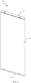
- FIG. 2 and FIG. 3 respectively show an overall structure and a split structure of the mobile phone 100.
- the mobile phone 100 may include a display 10, a rear cover 40, a middle frame 20, and a circuit board 30.
- the circuit board 30 may be disposed on a surface that is of the middle frame 20 and that faces the rear cover 40, and the display 10 and the rear cover 40 may be respectively located on two sides of the middle frame 20. Components are disposed at the top and the bottom of the mobile phone 100.
- the circuit board 30 may include a first circuit board 31 and a second circuit board 32.
- the first circuit board 31 and the second circuit board 32 may be electrically connected by using a flexible printed circuit or a leading wire.
- the first circuit board 31 may be located at an upper part of the middle frame 20, and the second circuit board 32 may be located at a lower part of the middle frame 20. In this way, interfaces disposed at the top and the bottom of the mobile phone 100 can be electrically connected to the circuit board 30.
- left and right sides of the display 10 curl toward the rear cover 40, so that the left and right sides of the electronic device are display regions of a screen.
- the mobile phone 100 has no black border in left and right directions, and a bezel-less "full view screen" is implemented on the left and right sides of the electronic device.
- the middle frame 20 includes a metal middle plate 22, a top frame 21, and a bottom frame 23.
- the top frame 21 and the bottom frame 23 may be respectively located at the top and the bottom of the metal middle plate 22.
- the top frame 21 and the bottom frame 23 are respectively located at the top and the bottom of the display 10 and the rear cover 40 (as shown in FIG. 2 ).
- the top frame 21 and the bottom frame 23 are exposed, and the metal middle plate 22 is located in space enclosed by the display 10, the rear cover 40, the top frame 21, and the bottom frame 23.
- a display surface of the mobile phone 100 has two frames: the top frame 21 and the bottom frame 23, there is no frame on side surfaces of the display surface, and the screen-to-body ratio of the mobile phone 100 may reach 95%.
- a material of the metal middle plate 22 includes but is not limited to an aluminum alloy, stainless steel, a steel-aluminum composite die-casting plate, or a titanium alloy.
- the top frame 21 and the bottom frame 23 may be metal frames, or the top frame 21 and the bottom frame 23 may be non-metal frames, for example, may be ceramic frames or glass frames.
- a material of the metal frames includes but is not limited to an aluminum alloy, stainless steel, a steel-aluminum composite die-casting plate, or a titanium alloy.
- the mobile phone 100 further includes brackets located on two sides of the metal middle plate 22, for example, a bracket 13a and a bracket 13b.
- the bracket 13a and the bracket 13b are located between the top frame 21 and the bottom frame 23.
- the bracket 13a may be connected to one side of the metal middle plate 22, and the bracket 13b may be connected to the other side of the metal middle plate 22.
- the bracket 13a and the bracket 13b may be connected to the metal middle plate 22 through clamping, adhesion, or fasteners (for example, screws).
- the bracket 13a and the bracket 13b may be non-metal brackets, for example, may be plastic brackets. In this way, a weight of the mobile phone 100 can be reduced.
- the display 10 may be a flexible display 10.
- the flexible display 10 may be an organic light-emitting diode (Organic Light-Emitting Diode, OLED) display.
- OLED Organic Light-Emitting Diode
- the display 10 may include a display layer 11 and a glass layer 12.
- the glass layer 12 covers the display layer 11, and a size of the glass layer 12 may be greater than or equal to a size of the display layer 11.
- the glass layer 12 may be a bendable glass layer.
- the display layer 11 may include a plurality of function layers.
- the plurality of function layers may be film layers such as an organic light-emitting layer, an anode layer, a cathode layer, and a thin film transistor (Thin Film Transistor, TFT) layer. Therefore, the display layer 11 includes a plurality of metal layers.
- the display 10 may further include a touch layer (not shown), and the touch layer may be disposed between the display layer 11 and the glass layer 12.
- the touch layer may be integrated into the display layer 11 to form a touch display panel integrating a touch function and a display function, and the glass layer 12 covers the touch display panel.
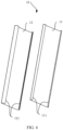
- curly parts are formed on the two sides of the display 10.
- first curly parts 121 are formed on two sides of the glass layer 12 in a curling process
- second curly parts 111 are formed on two sides of the display layer 11 in the curling process.
- the curly parts of the display 10 extend to the rear cover 40, and the rear cover 40 may be connected to the glass layer 12 of the display 10.
- a curling angle of the first curly part 121 of the glass layer 12 in the display 10 may be in a range of 90° to 180°.
- the curling angle of the first curly part 121 of the glass layer 12 in the display 10 may be 155°, and the two sides of the glass layer 12 curl from the display surface to the rear cover 40. In this way, both a left side surface and a right side surface of the mobile phone 100 belong to the glass layer 12.
- the curling angle of the first curly part 121 of the glass layer 12 may be 135°.
- the curling angle of the first curly part 121 may be any angle between 90° and 180°.
- a curling angle of the second curly part 111 of the display layer 11 in the display 10 may be in a range of 90° to 150°.
- the curling angle of the second curly part 111 of the display layer 11 in the display 10 may be 135°.
- the left and right side surfaces and partial rear surfaces of the electronic device are all display regions, so that a problem that the screen-to-body ratio is reduced due to existence of left and right black borders of the electronic device is avoided.
- the curling angle of the second curly part 111 of the display layer 11 in the display 10 may be any value between 150° and 180°.
- the curling angle of the second curly part of the display layer 11 may be 180°.
- the curling angle ranges of the first curly part 121 and the second curly part 111 may include endpoint values.
- the endpoint value 90° and the endpoint value 180° are included.
- the top frame 21 and the bottom frame 23 may be metal frames.
- a material of the top frame 21 and the bottom frame 23 may be an aluminum alloy, stainless steel, a steel-aluminum composite die-casting plate, or a titanium alloy.
- the rear cover 40 may be a glass rear cover.
- the top frame 21 and the bottom frame 23 may be used as radiators of an antenna.
- both the left side surface and the right side surface of the electronic device belong to the glass layer 12.
- neither the left side surface nor the right side surface of the electronic device can be used as an antenna.
- metal frames that can be used as antennas include only the top frame 21 and the bottom frame 23.
- a length of the metal frames that can be used as antennas is 150 mm.
- the length of the metal frames that can be used as antennas is reduced by approximately 30%. In this case, there is no sufficient length for arranging all antennas.
- an antenna bracket or an antenna separated from the top frame 21 and the bottom frame 23 is disposed at a position close to the curly part of the display 10 in the mobile phone 100 to increase an antenna length, because the display layer 11 of the display 10 has a metal layer, and the metal layer curls upward at the curly part, the metal layer in the display layer 11 shields a radiation aperture of a side antenna of the mobile phone 100, and consequently, radiation efficiency of the antenna disposed on the side of the mobile phone 100 is greatly reduced.
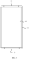
- each of the top frame 21 and the bottom frame 23 there are at least two gaps on each of the top frame 21 and the bottom frame 23.
- the gap a and the gap b divide the top frame 21 into a first radiator 211, a second radiator 212, and a third radiator 213 located between the first radiator 211 and the second radiator 212.
- the gap c and the gap d divide the bottom frame 23 into a fourth radiator 231, a fifth radiator 232, and a sixth radiator 233 located between the fourth radiator 231 and the fifth radiator 232.
- lengths L1 of the third radiator 213 and the sixth radiator 233 may be in a range of 50 mm to 60 mm.
- the length of the third radiator 213 may be 53 mm, or the length of the third radiator 213 may be 55 mm.
- the lengths of the third radiator 213 and the sixth radiator 233 may be the same or may be different.
- a minimum distance h1 between the metal middle plate 22 or the display layer 11 and each of the first radiator 211, the second radiator 212, and the third radiator 213 may be in a range of 1 mm to 1.4 mm.
- the minimum distance h1 between the metal middle plate 22 or the display layer 11 and each of the first radiator 211, the second radiator 212, and the third radiator 213 may be 1.2 mm, or may be 1.3 mm. In this way, it can be ensured that clearances of the first radiator 211, the second radiator 212, and the third radiator 213 may be in a range of 1 mm to 1.4 mm.
- a minimum distance h2 between the metal middle plate 22 or the display layer 11 and each of the fourth radiator 231, the fifth radiator 232, and the sixth radiator 233 may be in a range of 1.2 mm to 1.4 mm.
- the minimum distance h1 between the metal middle plate 22 or the display layer 11 and each of the fourth radiator 231, the fifth radiator 232, and the sixth radiator 233 may be 1.25 mm, or may be 1.35 mm. In this way, it can be ensured that clearances of the fourth radiator 231, the fifth radiator 232, and the sixth radiator 233 may be in a range of 1.2 mm to 1.4 mm.
- lengths L3 of the first radiator 211, the second radiator 212, the fourth radiator 231, and the fifth radiator 232 may be in a range of 8 mm to 10 mm.
- the lengths L3 of the first radiator 211, the second radiator 212, the fourth radiator 231, and the fifth radiator 232 may be 8.75 mm, or the lengths L3 of the first radiator 211, the second radiator 212, the fourth radiator 231, and the fifth radiator 232 may be 9 mm.
- the lengths of the first radiator 211, the second radiator 212, the fourth radiator 231, and the fifth radiator 232 may be the same or may be different.
- gap widths L2 of the gap a, the gap b, the gap c, and the gap d may be in a range of 1 mm to 1.5 mm.
- the gap widths L2 of the gap a, the gap b, the gap c, and the gap d may be 1.2 mm, or the gap widths L2 of the gap a, the gap b, the gap c, and the gap d may be 1.4 mm.
- the fourth radiator 231, the fifth radiator 232, and the sixth radiator 233 are radiation stubs of a main antenna (Main Antenna) of the mobile phone 100, clearances of the fourth radiator 231, the fifth radiator 232, and the sixth radiator 233 are greater than clearances of the first radiator 211, the second radiator 212, and the third radiator 213. This ensures that the main antenna of the mobile phone 100 has higher radiation efficiency.
- a plastic material may be injected into each gap and a spacing region between the frame and the metal middle plate in a nano-injection molding manner, so that each frame and the metal middle plate form an overall structure.
- At least one extension stub is further included.
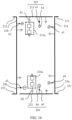
- four extension stubs are disposed: a first extension stub 21a, a second extension stub 21b, a fourth extension stub 23a, and a fifth extension stub 23b.
- One end of the first extension stub 21a is electrically connected to the first radiator 211, and the other end of the first extension stub 21a extends into space enclosed by the display 10 and the rear cover 40. In this way, the first extension stub 21a of a first antenna 201 is embedded inside the mobile phone.
- the first radiator 211 and the first extension stub 21a form a radiation stub of the first antenna 201.
- One end of the second extension stub 21b is electrically connected to the second radiator 212, and the other end of the second extension stub 21b extends into the space enclosed by the display 10 and the rear cover 40.
- the second radiator 212 and the second extension stub 21b form a radiation stub of a second antenna 202.
- One end of the fourth extension stub 23a is electrically connected to the fourth radiator 231, and the other end of the fourth extension stub 23a extends into the space enclosed by the display 10 and the rear cover 40.
- the fourth radiator 231 and the fourth extension stub 23a form a radiation stub of a fourth antenna 204.
- One end of the fifth extension stub 23b is electrically connected to the fifth radiator 232, and the other end of the fifth extension stub 23b extends into the space enclosed by the display 10 and the rear cover 40.
- the fifth radiator 232 and the fifth extension stub 23b form a radiation stub of a fifth antenna 205.
- a material of the first extension stub 21a, the second extension stub 21b, the fourth extension stub 23a, and the fifth extension stub 23b may be the same as or different from the material of the metal middle plate 22, the top frame 21, and the bottom frame 22.
- the material of the first extension stub 21a, the second extension stub 21b, the fourth extension stub 23a, and the fifth extension stub 23b may include but is not limited to an aluminum alloy, stainless steel, a steel-aluminum composite die-casting plate, or a titanium alloy.
- the first extension stub 21a, the second extension stub 21b, the fourth extension stub 23a, and the fifth extension stub 23b are added. In this way, the length of the antenna is increased, so that antenna length insufficiency is effectively compensated for.
- first extension stub 21a, second extension stub 21b, fourth extension stub 23a, and fifth extension stub 23b are located in the space enclosed by the display 10 and the rear cover 40, and the first radiator 211, the second radiator 212, the fourth radiator 231, and the fifth radiator 232 that are electrically connected to the first extension stub 21a, the second extension stub 21b, the fourth extension stub 23a, and the fifth extension stub 23b are located at the top and the bottom of the mobile phone 100.
- the first radiator 211, the second radiator 212, the fourth radiator 231, and the fifth radiator 232 can radiate outward, so that antenna radiation efficiency is ensured on the basis of extending the antenna.
- the other ends of the first extension stub 21a, the second extension stub 21b, the fourth extension stub 23a, and the fifth extension stub 23b may be connected to the metal middle plate 22 to implement grounding (because the metal middle plate 22 is electrically connected to a ground point of the circuit board 30), or may be connected to the ground point of the circuit board 30 to implement grounding.
- the first extension stub 21a, the second extension stub 21b, the fourth extension stub 23a, and the fifth extension stub 23b when the first extension stub 21a, the second extension stub 21b, the fourth extension stub 23a, and the fifth extension stub 23b are disposed in the space enclosed by the display 10 and the rear cover 40, the first extension stub 21a, the second extension stub 21b, the fourth extension stub 23a, and the fifth extension stub 23b may be disposed close to space enclosed by the second curly parts 111 of the display layer 11.
- the first extension stub 21a, the second extension stub 21b, the fourth extension stub 23a, and the fifth extension stub 23b may be wrapped by the second curly parts 111 of the display layer 11.
- first extension stub 21a, the second extension stub 21b, the fourth extension stub 23a, and the fifth extension stub 23b may be disposed in an extension manner in a direction parallel to an axial direction of the second curly parts 111.
- first extension stub 21a, the second extension stub 21b, the fourth extension stub 23a, and the fifth extension stub 23b may be disposed obliquely in the space enclosed by the display 10 and the rear cover 40.
- T-shaped radiation stubs may be formed.
- the mobile phone 100 may include at least one antenna, for example, may include one or more antennas.
- the mobile phone 100 may include six antennas: a first antenna 201, a second antenna 202, a third antenna 203, a fourth antenna 204, a fifth antenna 205, and a sixth antenna 206.
- the first antenna 201, the second antenna 202, and the third antenna 203 may be located at the top of the mobile phone 100, and the fourth antenna 204, the fifth antenna 205, and the sixth antenna 206 may be located at the bottom of the mobile phone 100.
- the second antenna 202 and the third antenna 203 may be diversity antennas (Div Antenna), and the first antenna 201 may be a Wi-Fi antenna, a Bluetooth antenna, and a GPS antenna.
- the first antenna 201 may be a dual-band antenna (the Wi-Fi antenna and the Bluetooth antenna use one band, and the GPS antenna uses another band).
- the fifth antenna 205 and the sixth antenna 206 may be main antennas (Main Antenna), and the fourth antenna may be a medium- and high-band multiple-input multiple-output (Multiple-Input Multiple-Output, MIMO) antenna.
- MIMO Multiple-Input Multiple-Output
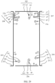
- the first antenna 201 may include the first radiator 211, the first extension stub 21a, a first feed b1, a first feed point a1, and a first ground point c1. Both the first feed point a1 and the first ground point c1 are electrically connected to the first extension stub 21a, the first feed b1 feeds a high-frequency current into the first extension stub 21a through the first feed point a1, and the high-frequency current is converted on the first extension stub 21a and the first radiator 211 and is transmitted in an electromagnetic wave manner.
- the first extension stub 21a and the first radiator 211 are the radiation stub of the first antenna 201.
- the second antenna 202 may include the second radiator 212, the second extension stub 21b, a second feed b2, a second feed point a2, and a second ground point c2. Both the second feed point a2 and the second ground point c2 are electrically connected to the second extension stub 21b.
- the second feed b2 is electrically connected to the second feed point a2, and the second extension stub 21b and the second radiator 212 are the radiation stub of the second antenna 202.
- Disposition of the first extension stub 21a and the second extension stub 21b increases lengths of the first antenna 201 and the second antenna 202, so that more antennas can be disposed.
- the third antenna 203 may include the third radiator 213, a third feed b3, a third feed point a3, and a third ground point c3. Both the third feed point a3 and the third ground point c3 are connected to the third radiator 213, and the third feed b3 is electrically connected to the third feed point a3.
- the first antenna 201, the second antenna 202, and the third antenna 203 disposed at the top of the mobile phone 100 respectively have the first feed point a1, the second feed point a2, and the third feed point a3.
- the antennas at the top of the mobile phone 100 have three independent feeding ports.
- One of the first antenna 201, the second antenna 202, and the third antenna 203 may be a low-band antenna, another one may be a medium- and high-band antenna, and the 3rd antenna may be a MIMO antenna covering medium and high frequencies.
- the first antenna 201 and the third antenna 203 may be diversity antennas (Div Antenna) covering low, medium, and high frequencies
- the second antenna 202 may be a MIMO antenna.
- the second antenna 202 and the third antenna 203 may be diversity antennas covering low, medium, and high frequencies
- the first antenna 201 may be a Bluetooth antenna (2400 MHz), a Wi-Fi antenna (2400 MHz), and a GPS antenna.
- the Bluetooth antenna, the Wi-Fi antenna, and the GPS antenna may share the first antenna 201, and the first antenna 201 is a dual-band antenna.
- the first antenna 201 or the second antenna 202 may be an antenna covering a 5G band, for example, an N77 band (3300 MHz to 4200 MHz) and an N79 band (4400 MHz to 5000 MHz) in the 5G band.
- a quantity of feeding ports disposed at the top of the mobile phone 100 includes but is not limited to three.
- the fourth antenna 204 may include the fourth radiator 231, the fourth extension stub 23a, a fourth feed b4, a fourth feed point a4, and a fourth ground point c4. Both the fourth feed point a4 and the fourth ground point c4 are electrically connected to the fourth extension stub 23a.
- the fourth extension stub 23a increases a length of the fourth antenna 204.
- the fifth antenna 205 may include the fifth radiator 232, the fifth extension stub 23b, a fifth feed b5, a fifth feed point a5, and a fifth ground point c5. Both the fifth feed point a5 and the fifth ground point c5 are electrically connected to the fifth extension stub 23b.
- the fifth extension stub 23b increases a length of the fifth antenna 205.
- the sixth antenna 206 may include the sixth radiator 233, a sixth feed b6, a sixth feed point a6, and a sixth ground point c6. Both the sixth feed point a6 and the sixth ground point c6 are connected to the sixth radiator 233.
- the fourth antenna 204, the fifth antenna 205, and the sixth antenna 206 disposed at the bottom of the mobile phone 100 respectively have the fourth feed point a4, the fifth feed point a5, and the sixth feed point a6.
- the antennas at the bottom of the mobile phone 100 have three independent feeding ports, so that the antennas at the bottom of the mobile phone 100 can be designed more freely.
- One of the fourth antenna 204, the fifth antenna 205, and the sixth antenna 206 may be a low-band antenna, another one may be a medium- and high-band antenna, and the 3rd antenna may be designed as an antenna that can cover medium and high frequencies. In this way, the three antennas at the bottom of the mobile phone 100 can cover more bands.
- the fifth antenna 205 and the sixth antenna 206 may be main antennas, and the fourth antenna may be a MIMO antenna or an antenna on a 5G band (for example, an N77 band (3300 MHz to 4200 MHz) and an N79 band (4400 MHz to 5000 MHz)).
- a 5G band for example, an N77 band (3300 MHz to 4200 MHz) and an N79 band (4400 MHz to 5000 MHz)
- Each feed and each feed point in FIG. 9 may be located on the circuit board 30, and each ground point may be electrically connected to a ground point of the metal middle plate 22 or the circuit board 30 to implement grounding.
- the third ground point c3 of the third antenna 203 when the third ground point c3 of the third antenna 203 is disposed, as shown in FIG. 9 , the third ground point c3 may be closer to the first radiator 211 compared with the second radiator 212.
- a horizontal distance L4 between the third ground point c3 and the gap b may be 2.6 mm
- a horizontal distance between the third ground point c3 and the gap a may be 53 mm.
- the third ground point c3 of the third antenna 203 may be close to the second radiator 212.
- the third ground point c3 of the third antenna 203 is disposed close to the first radiator 211 or the second radiator 212, so that interference caused by the third antenna 203 to a nearby radiator under different resonance is reduced. This ensures stable performance of the radiator close to the third ground point c3.
- the sixth ground point c6 of the sixth antenna 206 may be shown in FIG. 9 .
- a distance between the sixth ground point c6 and the fourth radiator 231 is shorter.
- a horizontal distance between the sixth ground point c6 and the gap d may be 2.6 mm
- a horizontal distance between the sixth ground point c6 and the gap c may be 53 mm.
- the sixth ground point c6 of the sixth antenna 206 may be close to the fifth radiator 232.
- the sixth ground point c6 of the sixth antenna 206 is disposed close to the fourth radiator 231 or the fifth radiator 232, so that performance of a radiator close to the sixth ground point c6 is not prone to be affected by the sixth antenna 206.
- the third antenna 203 may be a low-band antenna with an operating band of 700 MHz to 960 MHz.
- the first antenna 201 and the second antenna 202 may be medium- and high-band antennas with operating bands of 1805 MHz to 2690 MHz.
- the third antenna 203 and the second antenna 202 may be MIMO antennas covering low, medium, and high bands
- the first antenna 201 may be a dual-band antenna covering a Wi-Fi antenna (band: 2400 MHz to 2500 MHz) and a GPS antenna (operating band: 1575 ⁇ 100 MHz).
- the first antenna 201 may be a medium- and high-band MIMO antenna.
- the sixth antenna 206 may be a low-band antenna.
- the fourth antenna 204 and the fifth antenna 205 may be medium- and high-band antennas.
- the sixth antenna 206 and the fifth antenna 205 may be main antennas covering low, medium, and high bands (for example, the low band is 700 MHz to 960 MHz, the medium band is 1710 MHz to 2200 MHz, and the high band is 2300 MHz to 2700 MHz), and the fourth antenna 204 may be a medium- and high-band MIMO antenna.
- the fourth antenna 204 may be a dual-band antenna covering a Wi-Fi antenna and a GPS antenna.
- types of the first antenna 201, the second antenna 202, the third antenna 203, the fourth antenna 204, the fifth antenna 205, and the sixth antenna 206 include but are not limited to the foregoing antennas.
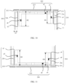
- a length H1 of the first extension stub 21a may be in a range of 10 mm to 25 mm.
- the length H1 of the first extension stub 21a may be 23 mm, or the length H1 of the first extension stub 21a may be 11 mm.
- a length H2 of the second extension stub 21b may be in a range of 10 mm to 25 mm.
- the length H2 of the second extension stub 21b may be 18 mm, or the length H1 of the first extension stub 21a may be 22 mm.
- the first extension stub 21a and the second extension stub 21b are respectively radiation stubs of the first antenna 201 and the second antenna 202, and when the first extension stub 21a and the second extension stub 21b are disposed inside the mobile phone 100, clearances of the first extension stub 21a and the second extension stub 21b are not less than 0.5 mm.
- a minimum distance h3 between the second extension stub 21b and an inner wall of the display layer 11 may be 0.5 mm.
- a length H4 of the fourth extension stub 23a may be in a range of 10 mm to 25 mm.
- the length H4 of the fourth extension stub 23a may be 23 mm, or the length H4 of the fourth extension stub 23a may be 11 mm.
- a length H3 of the fifth extension stub 23b may be in a range of 10 mm to 25 mm.
- the length H3 of the fifth extension stub 23b may be 18 mm, or the length H3 of the fifth extension stub 23b may be 22 mm.
- Clearances of the fourth extension stub 23a and the fifth extension stub 23b are not less than 0.5 mm.
- a minimum distance between the fourth extension stub 23a and the inner wall of the display layer 11 may be 0.5 mm. This ensures that the fourth extension stub 23a and the fifth extension stub 23b have clearance regions inside the mobile phone 100, so that the fourth extension stub 23a and the fifth extension stub 23b have good radiation efficiency.
- each extension stub may be connected to a corresponding radiator through welding, clamping, a fastener (for example, a screw), or integral molding.
- the first radiator 211 has a mounting part 211a.
- a plug part 211c that can be plugged into the mounting part 211a exists at an end that is of the first extension stub 21a and that is connected to the first radiator 211.
- the plug part 211c is connected to the mounting part 211a through a fastener (for example, a screw or a bolt). In this way, the first extension stub 21a is fastened to the first radiator 211.
- connection manner shown in FIG. 13 may also be used between the remaining three extension stubs and corresponding radiators.
- the four extension stubs and the corresponding radiators may be connected by using, but not limited to, the connection manner between the mounting part 211a and the plug part 211c, or may be connected by using another fitting structure.
- the first extension stub 21a, the second extension stub 21b, the extension stub of the third antenna 203, and the fourth extension stub 23a each are in a suspended bridge structure in the mobile phone 100.
- one end of the first extension stub 21a is connected to the first radiator 211
- the other end of the first extension stub 21a is connected to the metal middle plate 22
- the first extension stub 21a is in a suspended bridge structure between the first radiator 211 and the metal middle plate 22.
- each extension stub may be a suspended bridge structure formed by extending a part of an edge of the metal middle plate 22 toward a corresponding radiator.
- FIG. 13 each extension stub may be a suspended bridge structure formed by extending a part of an edge of the metal middle plate 22 toward a corresponding radiator.
- a side edge of the metal middle plate 22 extends to the first radiator 211 in a suspended manner and is connected to the first radiator 211.
- a suspended bridge structure is excavated in a region that is of the metal middle plate 22 and that is close to the first radiator 211, and is used as the first extension stub 21a.
- one end of the first extension stub 21a is integrated with the metal middle plate 22, and the first ground point c1 is located on the metal middle plate 22. This avoids a case in which a spring plate is disposed between the first extension stub 21a and the metal middle plate 22 for grounding.
- a feed point structure may be disposed on the radiator or the extension stub.
- a feed point structure 211b is disposed on the first extension stub 21a, and the first feed point a1 is electrically connected to a spring plate a11.
- the spring plate a11 abuts the feed point structure 211b to implement an electrical connection.
- the remaining feed points each may also be connected to a spring plate, a feed point structure abutting the spring plate is disposed on a radiator or an extension stub, and each feed point is electrically connected to the extension stub or the radiator through abutting between the spring plate and the feed point structure.
- connection structure 111a is disposed at the display layer 11.
- the circuit board 30 and the display layer 11 may be connected by using the connection structure 111a and a fastener (for example, screw).
- a fastener for example, screw
- the connection structure 111a of the display layer 11 is connected to the ground point of the circuit board 30 by using the fastener. In this way, the display layer 11 is grounded.
- the third antenna 203 may further include a first tuning contact d1, and the first tuning contact d1 is configured to connect the third radiator 213 to a matching circuit.
- the sixth antenna 206 may further include a second tuning contact d2, and the second tuning contact d2 is configured to connect the third radiator 213 to a matching circuit.
- the first tuning contact d1 and the second tuning contact d2 may be conductive sheets connected to the third radiator 213 and the sixth radiator 233.
- positions at which the first tuning contact d1 and the second tuning contact d2 are connected to the third radiator 213 and the sixth radiator 233 are specifically set based on a tuning width.
- a longer distance between the position at which the first tuning contact d1 is connected to the third radiator 213 and a position at which the third feed point a3 is connected to the third radiator 213 indicates a larger tuning range.
- this affects radiation efficiency. Therefore, when a required band can be covered during tuning, the position at which the first tuning contact d1 is connected to the third radiator 213 may be set close to the position at which the third feed point a3 is connected to the third radiator 213. In this way, high radiation efficiency can be achieved.
- the sixth antenna 206 is a low-band antenna of a main antenna
- the third antenna 203 is a MIMO antenna
- a distance between points at which the sixth radiator 233 is connected to the second tuning contact d2 and the sixth feed point a6 is greater than a distance between points at which the third radiator 213 is connected to the first tuning contact d1 and the third feed point a3.
- the third radiator 213 is electrically connected to a first tuning circuit 213a through the first tuning contact d1.
- the sixth radiator 233 is electrically connected to a second tuning circuit 216a through the second tuning contact d2.
- the third antenna 203 may switch to paths corresponding to different low bands. In this way, a bandwidth of the third antenna 203 can cover all of a bandwidth of 700 MHz to 960 MHz.
- the sixth antenna 206 may switch to paths corresponding to different low bands. This ensures that a bandwidth of the sixth antenna 206 can cover all of a bandwidth of 700 MHz to 960 MHz.
- the first tuning circuit 213a and the second tuning circuit 216a each may include a tuning switch and at least one matching circuit, one end of the matching circuit is connected to the tuning switch, and the other end of the matching circuit is grounded.
- the tuning switch may be one or more switches. Any switch may be a single-input multiple-output single-pole multi-throw switch, or may be a multiple-input multiple-output multi-pole multi-throw switch. This is not limited in this application. Any switch may be one or more switches connected in series and/or in parallel. This is not limited in this application.
- the matching circuit may be one capacitor, one inductor, a plurality of capacitors connected in series, a plurality of inductors connected in series, a plurality of capacitors connected in parallel, a plurality of inductors connected in parallel, at least one capacitor and at least one inductor that are connected in series, or at least one group of serially connected capacitors and at least one group of serially connected inductors that are connected in parallel. This is not limited in this application.
- the first tuning circuit 213a includes a first tuning switch 2135 and four matching circuits: a first matching circuit 2131, a second matching circuit 2132, a third matching circuit 2133, and a fourth matching circuit 2134.
- the first tuning switch 2135 may be a single-pole four-throw switch (for example, SP4T), and the first tuning switch 2135 has four switching paths, for example, RF1, RF2, RF3, and RF4.
- the first matching circuit 2131, the second matching circuit 2132, the third matching circuit 2133, and the fourth matching circuit 2134 respectively correspond to RF1, RF2, RF3, and RF4.
- the first tuning switch 2135 is switched to RF4.
- the fourth matching circuit 2134 connected on the path RF4 is an inductor of 18 nH. A larger inductance of a connected inductor indicates a lower resonance frequency.
- B28a is a band covered when the first tuning switch 2135 is switched to RF1 and is connected to a capacitor of 0.3 pF
- B28a is a band covered by the sixth antenna 206 after all paths of the first tuning switch 2135 are disconnected.
- the bandwidth of the sixth antenna 206 covers the entire bandwidth of the low band of 700 MHz to 960 MHz by using the foregoing four matching circuits.
- antennas in the following scenario 1 and scenario 2 are used as examples to perform simulation test.
- the glass layer 12 of the display 10 curls by 180°
- the display layer 11 curls by 135°
- the screen-to-body ratio reaches 95%.
- Clearances of the antennas: the fourth antenna 204, the fifth antenna 205, and the sixth antenna 206 at the bottom of the mobile phone 100 are less than or equal to 1.35 mm.
- a total length of the bottom frame 23 of the mobile phone 100 is 73.5 mm
- widths of the gap c and the gap d are 1.5 mm
- a length of the sixth radiator 233 is 53 mm
- lengths of the fourth radiator 231 and the fifth radiator 232 are 8.75 mm
- lengths of the fourth extension stub 23a and the fifth extension stub 23b are 14.25 mm. Therefore, antenna radiation lengths of the fifth antenna 205 and the fourth antenna 204 are 23 mm.
- the sixth ground point c6 of the sixth antenna 206 is disposed close to the fourth radiator 231.
- the sixth antenna 206 is disposed as a low-band antenna.
- the sixth antenna 206 is connected to a tuning circuit and has a frequency tuning function. A bandwidth of approximately 80 MHz needs to be covered in each tuning state.
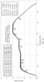
- efficiency of the sixth antenna 206 in different tuning states is shown in FIG. 18.
- FIG. 18 shows antenna simulation efficiency of the sixth antenna 206 in different tuning states. It can be learned from FIG. 18 that average efficiency of the sixth antenna 206 in each of B28a, B28b, B20, B5, and B8 is higher than -5.5 dB. Average efficiency of an existing low-band antenna is -7 dB. Therefore, in this embodiment of this application, the average efficiency of the sixth antenna 206 in different tuning states is higher than the average efficiency of the existing low-band antenna by 1.5 dB.
- the fourth antenna 204 is disposed as a high-band antenna
- the fifth antenna 205 is disposed as a medium- and high-band antenna.
- FIG. 19 shows radiation efficiency of the fourth antenna 204 and the fifth antenna 205 in different tuning states of the sixth antenna 206. It can be learned from FIG. 19 that in different tuning states of the sixth antenna 206, the radiation efficiency of the fourth antenna 204 may be available to cover 2300 MHz to 2690 MHz. Average efficiency of the fourth antenna 204 is -4.5 dB in the band of 2300 MHz to 2690 MHz.
- the radiation efficiency of the fifth antenna 205 may be available to cover 1710 MHz to 2690 MHz.
- efficiency of the fifth antenna 205 decreases near B12 (2600 MHz). A reason is that the ground point of the sixth antenna 206 is far away from the fifth antenna 205, and stability of the fifth antenna 205 is affected during tuning of the sixth antenna 206.
- the fifth antenna 205 is in the band of 1710 MHz to 2690 MHz, and average efficiency of the fifth antenna 205 at B3 (1800 MHz), B1 (2100 MHz), and B7 (2600 MHz) is still higher than -5.5 dB after switch and component losses are considered. Therefore, in this embodiment of this application, when the fourth antenna 204 is a high-band antenna, and the fifth antenna 205 is a medium- and high-band antenna, the fourth antenna 204 and the fifth antenna 205 still have good bandwidths and radiation efficiency with respect to a relatively small clearance and blocking by the curly part of the display layer 11.
- the fourth antenna 204 is disposed as a medium- and high-band antenna.
- the fourth antenna 204 is disposed as a medium- and high-band MIMO antenna.
- FIG. 20 shows radiation efficiency of the fourth antenna 204 disposed as a medium- and high-band MIMO antenna. It can be learned from FIG. 20 that the radiation efficiency of the fourth antenna 204 may be available to cover a band of 1805 MHz to 2690 MHz.
- the fourth antenna 204 is disposed as a medium- and high-band MIMO antenna, a bandwidth of the fourth antenna 204 is extended. Therefore, average radiation efficiency of the fourth antenna 204 is lower than average radiation efficiency of the medium- and high-band antenna in FIG. 19 . It can be learned from FIG.
- average efficiency of the fourth antenna 204 in a receive (Rx) band of B3 (1800 MHz) is higher than -7.5 dB
- average efficiency of the fourth antenna 204 in an Rx band of B1 (2100 MHz) is -7.3 dB
- average efficiency of the fourth antenna 204 in an Rx band of B7 is -6.5 dB. Therefore, when the fourth antenna 204 is disposed as a medium- and high-band MIMO antenna, radiation efficiency of the medium- and high-band MIMO antenna decreases by approximately 2 dB compared with radiation efficiency of the fourth antenna 204 disposed as the high-band antenna in FIG. 19 and radiation efficiency of the medium- and high-band antenna in FIG.
- the decrease of 2 dB in the radiation efficiency does not affect normal operation of the antenna. Therefore, in this embodiment of this application, radiation efficiency of the fifth antenna 205 disposed as a medium- and high-band antenna is higher than radiation efficiency of the fourth antenna 204 disposed as a medium- and high-band antenna. Therefore, the fifth antenna 205 may be a main antenna and cover medium and high bands of the main antenna, and the fourth antenna 204 may be a medium- and high-band MIMO antenna because radiation efficiency of the MIMO antenna may be 3 dB lower than radiation efficiency of the main antenna.
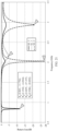
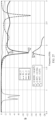
- FIG. 21 shows initial resonances of the fourth antenna 204 and the fifth antenna 205 disposed as medium- and high-band antennas and the sixth antenna 206 disposed as a low-band antenna.
- S3,3 is a return loss curve of the sixth antenna 206
- S1,1 is a return loss curve of the fourth antenna 204
- S2,2 is a return loss curve of the fifth antenna 205. It can be learned from FIG. 21 that when the sixth antenna 206 is a low-band antenna, a resonance is at 0.84 GHz, and when the fourth antenna 204 is a medium- and high-band antenna, a resonance is at 2.15 GHz.
- the fifth antenna 205 is a medium- and high-band antenna, there are two resonances, which are respectively at 2.03 GHz and 2.93 GHz.
- the low-band antenna needs a length of approximately 70 mm to generate a 0.84 GHz low-frequency resonance.
- the length of the sixth radiator 233 of the sixth antenna 206 is 53 mm, but a 0.84 GHz resonance is excited. Therefore, it can be learned that in addition to the sixth radiator 233, another radiator is further used for the sixth antenna 206.
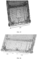
- FIG. 22 shows current distribution during low-frequency resonance (0.84 GHz) of the sixth antenna 206. It can be learned from FIG. 22 that the fifth radiator 232, the fifth extension stub 23b, and the sixth radiator 233 form an in-phase current (1/4 wavelength).
- the 1.5 mm gap c between the fifth radiator 232 and the sixth radiator 233 does not block distribution of the in-phase current.
- the sixth antenna 206 uses a radiating element of the fifth antenna 205.
- the sixth radiator 233, the fifth radiator 232, and the fifth extension stub 23b are used together, so that the sixth antenna 206 excites a 0.84 GHz resonance in a length of 53 mm. Therefore, in this embodiment of this application, a length of the low-band antenna is shortened compared with that in the conventional technology.
- FIG. 23 shows current distribution on the middle frame 20, a left curly part of the display layer 11 of the display 10, and a frame (for example, the top frame 21, the bottom frame 23, and each extension stub) during low-frequency resonance (0.84 GHz) of the sixth antenna 206. It can be learned from FIG. 23 that current distribution on a curly side of the display layer 11 and the frame is in-phase, to form ring-shaped current distribution.
- main radiation is floor radiation (that is, radiation by a metal plate through which the low-band antenna is grounded). Therefore, this type of current distribution facilitates radiation of the low-band antenna.
- FIG. 24 shows initial radiation efficiency of the fourth antenna 204 disposed as a medium- and high-band antenna and efficiency of the fourth antenna 204 disposed as a Wi-Fi antenna and a GPS antenna.
- a resonance of the fourth antenna 204 is at 2.15 GHz
- initial radiation efficiency of the fourth antenna 204 reaches -2.3 dB at 1.54 GHz. Therefore, the fourth antenna 204 has a good bandwidth characteristic. In a band of 1.5 GHz to 2.7 GHz, efficiency is higher than -2.5 dB. Therefore, different matching circuits are used, and the fourth antenna 204 may be disposed as a medium- and high-band antenna, or may be disposed as a GPS antenna and a Wi-Fi antenna.
- the fourth antenna 204 is not a common inverted F antenna (Invert F Antenna, IFA). Because of an antenna length of 23 mm, in a GPS band (1557 MHz to 1601 MHz), there is no initial radiation efficiency higher than -2.0 dB.
- IFA Invert F Antenna
- FIG. 25 shows current distribution during resonance of the fourth antenna 204.
- the fourth antenna 204 forms half-wavelength current distribution on the bottom frame 23 of the mobile phone 100. This indicates that radiation of the fourth antenna 204 is from the sixth radiator 233 and a radiating element of the fourth antenna 204. Main radiation is from the sixth radiator 233. Therefore, in this embodiment of this application, the fourth antenna 204 uses a radiating element of the sixth antenna 206. Thus, even if the fourth extension stub 23a in the fourth antenna 204 is blocked by the curly part of the display layer 11, radiation efficiency of the fourth antenna 204 is relatively high.
- the fourth extension stub 23a and the fourth radiator 231 are not main radiating elements of the fourth antenna 204, currents on the fourth extension stub 23a and the fourth radiator 231 cross the gap d, and the radiating element of the sixth antenna 206 is used for radiation. Therefore, in this embodiment of this application, it is ensured that the fourth antenna 204 has a good bandwidth and good radiation efficiency.
- FIG. 26 shows current distribution during resonance of the fifth antenna 205.
- the fifth antenna 205 forms a 3/4 ⁇ current mode on the sixth radiator 233. This indicates that the fifth antenna 205 uses the sixth radiator 233.
- the fifth extension stub 23b connected to the fifth feed point a5 and the fifth radiator 232 that are in the fifth antenna 205 are not main radiating elements of the fifth antenna 205, a main radiating element of the fifth antenna 205 is the sixth radiator 233, the fifth antenna 205 reuses a stub of the sixth antenna 206 for radiation.
- the fourth antenna 204 and the fifth antenna 205 use the radiation stub of the sixth antenna 206.
- This overcomes a problem that antenna efficiency is reduced because the curly part blocks the antenna when the display 10 curls.
- the sixth antenna 206 uses the radiation stub of the fifth antenna 205, so that the length of the sixth antenna 206 is reduced.
- FIG. 27 shows efficiency and isolation curves existing when the fourth antenna 204 and the fifth antenna 205 are disposed as two medium- and high-band antennas and the sixth antenna 206 is disposed as a low-band antenna.
- S3,3 is a return loss curve obtained after a matching circuit is added to the sixth antenna 206
- S2,2 is a return loss curve obtained after a matching circuit is added to the fifth antenna 205
- S1,1 is a return loss curve obtained after a matching circuit is added to the fourth antenna 204
- S1,2 is an isolation curve of the fifth antenna 205 and the fourth antenna 204.
- the mobile phone 100 may further include at least one high-band antenna.
- the mobile phone 100 may further include the seventh antenna 207 and the eighth antenna 208.
- the seventh antenna 207 may include a seventh radiator 214, a seventh feed point a7, a seventh feed b7, and a seventh ground point c7.
- the seventh radiator 214 is electrically connected to the seventh feed point a7 and the seventh ground point c7, and the seventh feed b7 feeds a high-frequency current into the seventh radiator 214 through the seventh feed point a7. As shown in FIG.
- the seventh radiator 214 may be disposed along an inner side of the first extension stub 21a (that is, a surface that is of the first extension stub 21a and that faces the second extension stub 21b).
- a minimum distance between the seventh radiator 214 and the first extension stub 21a is greater than or equal to 0.5 mm. This ensures that a clearance of the seventh radiator 214 is greater than or equal to 0.5 mm.
- the eighth antenna 208 may include an eighth radiator 215, an eighth feed point a8, an eighth feed b8, and an eighth ground point c8.
- the eighth radiator 215 is electrically connected to the eighth feed point a8 and the eighth ground point c8, and the eighth feed b8 feeds a high-frequency current into the eighth radiator 215 through the eighth feed point a8.
- the eighth radiator 215 may be disposed along an inner side of the second extension stub 21b (that is, a surface that is of the second extension stub 21b and that faces the first extension stub 21a).
- a minimum distance between the eighth radiator 215 and the second extension stub 21b is greater than or equal to 0.5 mm. This ensures that a clearance of the eighth radiator 215 is greater than or equal to 0.5 mm.
- the seventh antenna 207 and the eighth antenna 208 have corresponding feed points.
- the antennas at the top of the mobile phone 100 have at least five independent feeding ports, so that antenna modes are richer, and antenna setting is more flexible.
- the seventh antenna 207 and the eighth antenna 208 may be Wi-Fi 5G antennas.
- An operating band of the Wi-Fi 5G antenna may be 4900 MHz to 5900 MHz.
- the seventh antenna 207 and the eighth antenna 208 may be antennas covering 5G bands.
- operating bands of the seventh antenna 207 and the eighth antenna 208 may be 3300 MHz to 3600 MHz and 4800 MHz to 5000 MHz. It should be noted that the operating bands of the seventh antenna 207 and the eighth antenna 208 include but are not limited to a band above or below 6 GHz in a 5G band.
- FIG. 30 shows radiation efficiency existing when the seventh antenna 207 is a Wi-Fi 5G antenna. As shown in FIG. 30 , average efficiency in an entire band is higher than -5 dB. Therefore, when the seventh antenna 207 is located inside the mobile phone 100, the seventh antenna 207 has good radiation efficiency.
- the operating bands of the seventh antenna 207 and the eighth antenna 208 are relatively high. Therefore, the two antennas do not disturb the three existing antennas. In this way, the seventh antenna 207 and the eighth antenna 208 are antennas suitable for a 5G system (3.3 GHz to 5 GHz).
- positions at which the seventh antenna 207 and the eighth antenna 208 are disposed include but are not limited to the inner sides of the first extension stub 21a and the second extension stub 21b.
- the seventh antenna 207 and the eighth antenna 208 may alternatively be disposed along the fourth extension stub 23a and the fifth extension stub 23b.
- the seventh antenna 207, the eighth antenna 208, a ninth antenna (not shown), and a tenth antenna (not shown) may be disposed respectively along inner sides of the first extension stub 21a, the second extension stub 21b, the fourth extension stub 23a, and the fifth extension stub 23b.
- the ninth antenna and the tenth antenna each have a corresponding feed point.
- the antennas at the top of the mobile phone 100 have five independent feeding ports
- the antennas at the bottom of the mobile phone 100 have five independent feeding ports
- 10 antennas may be disposed in the mobile phone 100.
- a quantity of feeding ports of the antennas in the mobile phone 100 includes but is not limited to 10.
- the seventh feed point a7 of the seventh antenna 207 and the eighth feed point a8 of the eighth antenna 208 may be located on the circuit board 30, and the seventh ground point c7 and the eighth ground point c8 may be connected to the ground point of the circuit board 30, or connected to the metal middle plate 22 to implement grounding.
- the seventh antenna 207 and the eighth antenna 208 may be suspended inside the mobile phone 100, or the seventh antenna 207 and the eighth antenna 208 may be located on the circuit board 30, or the seventh antenna 207 and the eighth antenna 208 may be suspended on the metal middle plate 22.
- the referred apparatus or component needs to have a specific azimuth, be constructed and operated in a specific azimuth, and therefore cannot be understood as a limitation to embodiments of this application.
- the meaning of "a plurality of" is two or more, unless otherwise precisely and specifically specified.
Landscapes
- Engineering & Computer Science (AREA)
- Computer Networks & Wireless Communication (AREA)
- Signal Processing (AREA)
- Support Of Aerials (AREA)
- Telephone Set Structure (AREA)
- Medicines That Contain Protein Lipid Enzymes And Other Medicines (AREA)
Description
- This application relates to the field of terminal technologies, and in particular, to an antenna assembly and an electronic device with a rollable display.
- A mobile communications network provided by an operator is needed for communication between intelligent terminals such as mobile phones. A communication connection between intelligent devices can further be implemented in a plurality of manners such as wireless fidelity (Wireless Fidelity, Wi-Fi), Bluetooth, and infrared. For a mobile phone, communication signals are sent and received through antennas. Because the mobile phone performs communication in various manners, a relatively large quantity of antennas need to be disposed inside the mobile phone.
- Currently, when the antennas are disposed in the mobile phone, as shown in
FIG. 1 , specifically, gaps are disposed at a top part and a bottom part of ametal frame 1 of the mobile phone, to form a first antenna 1a and asecond antenna 1b. The first antenna 1a includes a top metal frame and parts of metal side frames, and thesecond antenna 1b includes a bottom metal frame and parts of the metal side frames. - When side frames of a mobile phone are non-metal frames, for example, when the side frames of the mobile phone are glass frames, a total length of metal frames that can be used as antennas is reduced. Consequently, there is no sufficient length space in the mobile phone for arranging all antennas.
US 2019/067796 A1 describes a mobile device that includes a ground element, a first radiation element, a second radiation element, a matching circuit, and a first metal frame.
WO 2019/068331 A1 describes an antenna system for a mobile device that includes a first electrically conductive member having a plurality of segments including at least a first corner segment and a central segment that is disposed adjacent to the first corner segment.
US 2018/026338 A1 describes an antenna structure that includes a metal housing, a first resonance portion, a second resonance portion, an extending portion, and a signal feed source.
WO 2019/100202 A1 describes an antenna comprising an antenna body and an antenna branch, wherein one end of the antenna branch is connected to the antenna body, and the other end thereof is connected to a feed point of a main radio frequency path; the end of the antenna branch which is connected to the feed point of the main radio frequency path is also connected to the antenna body by means of a first adjustable device; and the first adjustable device comprises an off state and an on state.
CN 204 538 197 U describes a portable wireless telecom equipment's metal frame antenna.
US 2018/241115 A1 describes an electronic device including a support member on which an antenna radiator is formed. - This application provides an antenna assembly and an electronic device with a rollable display, to increase a length of an antenna, ensure radiation efficiency of the antenna, and resolve a problem in an existing mobile phone that a length for arranging antennas in the mobile phone is insufficient due to reduction of metal frames that can be used as antennas.
In accordance with the invention, there is provided an electronic device as device in the appended claims. - A first aspect provides an antenna assembly, used in an electronic device. The antenna assembly includes a first antenna, and the first antenna includes a first radiator, a first extension stub, and a first feed point and a first ground point that are electrically connected to the first extension stub. One end of the first extension stub is connected to the first radiator, the other end of the first extension stub extends into the electronic device, and the first radiator is a part of a top metal frame or a part of a bottom metal frame of the electronic device.
- The first antenna includes the first radiator and the first extension stub connected to the first radiator, and the first radiator is located on the top metal frame or the bottom metal frame of the electronic device. In this way, the first radiator can radiate an electromagnetic wave to the outside, so that radiation efficiency of the first antenna is ensured. The first extension stub extends into the electronic device. In this way, when a side edge of the electronic device is a non-metal frame, disposition of the first extension stub increases a length of the first antenna. This ensures that the first antenna has a sufficient length, and ensures that an antenna with a sufficient length can be disposed in the electronic device. Therefore, a problem in an existing mobile phone that a length for arranging antennas in the mobile phone is insufficient due to reduction of metal frames that can be used as antennas is resolved.
- In a possible implementation, the antenna assembly further includes a second antenna. The second antenna includes at least a second radiator, a second extension stub, and a second feed point and a second ground point that are electrically connected to the second extension stub, one end of the second extension stub is connected to the second radiator, and the other end of the second extension stub extends into the electronic device.
- The first radiator is located at one end of the top metal frame, and the second radiator is located at the other end of the top metal frame.
- Alternatively, the first radiator is located at one end of the bottom metal frame, and the second radiator is located at the other end of the bottom metal frame. Alternatively, the first radiator is located at one end of the top metal frame, and the second radiator is located at one end of the bottom metal frame; or the first radiator is located at one end of the bottom metal frame, and the second radiator is located at one end of the top metal frame.
- The second extension stub is disposed, so that the second extension stub increases a length of the second antenna. This ensures that the second antenna has a sufficient length.
- In a possible implementation, the antenna assembly further includes a third antenna. The third antenna includes at least a third radiator and a third feed point and a third ground point that are electrically connected to the third radiator.
- The third radiator is located between the first radiator and the second radiator, a first gap exists between one end of the third radiator and the first radiator, a second gap exists between the other end of the third radiator and the second radiator.
- In this way, the third antenna may use a radiation stub of the first antenna or the second antenna, and the first antenna and the second antenna may use the radiator of the third antenna for radiation, to ensure that the third antenna, the first antenna, and the second antenna excite corresponding resonance frequencies when lengths of the third antenna, the first antenna, and the second antenna are relatively small.
- In a possible implementation, the antenna assembly further includes a fourth antenna. The fourth antenna includes at least a fourth radiator, a fourth extension stub, and a fourth feed point and a fourth ground point that are electrically connected to the fourth extension stub.
- One end of the fourth extension stub is connected to the fourth radiator, the other end of the fourth extension stub extends into the electronic device, one of the fourth radiator and the first radiator is a part of the top metal frame, and the other is a part of the bottom metal frame.
- A length of the fourth antenna is increased by using the fourth extension stub, to ensure that more antennas can be disposed in the electronic device.
- In a possible implementation, the antenna assembly further includes a fifth antenna. The fifth antenna includes at least a fifth radiator, a fifth extension stub, and a fifth feed point and a fifth ground point that are electrically connected to the fifth extension stub, one end of the fifth extension stub is connected to the fifth radiator, and the other end of the fifth extension stub extends into the electronic device.
- The fourth radiator is located at one end of the top metal frame, and the fifth radiator is located at the other end of the top metal frame; or the fourth radiator is located at one end of the bottom metal frame, and the fifth radiator is located at the other end of the bottom metal frame. Alternatively, one of the fourth radiator, the fifth radiator, the first radiator, and the second radiator is located at one end of the top metal frame, another one is located at the other end of the top metal frame, the 3rd one is located at one end of the bottom metal frame, and the 4th one is located at the other end of the bottom metal frame.
- A length of the fifth antenna is increased by using the fifth extension stub, to ensure that an enough long antenna can be disposed in the electronic device.
- In a possible implementation, the antenna assembly further includes a sixth antenna. The sixth antenna includes at least a sixth radiator and a sixth feed point and a sixth ground point that are electrically connected to the sixth radiator.
- The sixth radiator is located between the fourth radiator and the fifth radiator, there is a gap between one end of the sixth radiator and the fourth radiator, and a third gap exists between one end of the sixth radiator and the fourth radiator, a fourth gap exists between the other end of the sixth radiator and the fifth radiator. The sixth antenna is disposed, and the radiator of the sixth antenna is located between the fifth antenna and the fourth antenna. In this way, the sixth antenna may use a radiation stub of the fourth antenna or the fifth antenna, and the fourth antenna and the fifth antenna may use the radiator of the sixth antenna for radiation, to ensure that the sixth antenna, the fifth antenna, and the fourth antenna excite corresponding resonance frequencies when lengths of the sixth antenna, the fifth antenna, and the fourth antenna are relatively small.
- In a possible implementation, the third antenna further includes a first tuning circuit, one end of the first tuning circuit is electrically connected to the third radiator through a first tuning contact, and the other end of the first tuning circuit is grounded.
- The sixth antenna further includes a second tuning circuit, one end of the second tuning circuit is electrically connected to the sixth radiator through a second tuning contact, and the other end of the second tuning circuit is grounded.
- The first tuning circuit can enable the third antenna to cover an entire bandwidth of a low band when the third antenna is used as a low-band antenna, and the second tuning circuit can enable the sixth antenna to cover an entire bandwidth of a low band when the sixth antenna is used as a low-band antenna.
- In a possible implementation, the first tuning circuit and the second tuning circuit each include a tuning switch and at least one matching circuit, one end of the matching circuit is electrically connected to the tuning switch, and the other end of the matching circuit is grounded. The third antenna and the sixth antenna can be switched to matching paths with different load by using tuning switches, so that the third antenna and the sixth antenna cover more bandwidths.
- In a possible implementation, the first radiator, the second radiator, and the third radiator are three metal frames formed by disposing two gaps on the top metal frame.
- The fourth radiator, the fifth radiator, and the sixth radiator are three metal frames formed by disposing two gaps on the bottom metal frame.
- In this way, the top metal frame may be used as the first radiator, the second radiator, and the third radiator to transmit an electromagnetic wave to the outside, and the bottom metal frame may be used as the fourth radiator, the fifth radiator, and the sixth radiator. This avoids additionally disposing an antenna radiator in the electronic device. In addition, when the top metal frame and the bottom metal frame are used as antenna radiators, because the top metal frame and the bottom metal frame are located at the top and the bottom of the electronic device, radiation efficiency is relatively high.
- In a possible implementation, the first extension stub, the second extension stub, the fourth extension stub, and the fifth extension stub each are in a suspended bridge structure in the electronic device.
- This ensures that the first extension stub, the second extension stub, the fourth extension stub, and the fifth extension stub have appropriate clearances in the electronic device.
- In a possible implementation, the first extension stub, the second extension stub, the fourth extension stub, and the fifth extension stub are four metal stubs formed by ea metal middle plate in the electronic device separately extending toward the top metal frame and the bottom metal frame.
- In this way, the metal middle plate is integrated with the first extension stub, the second extension stub, the fourth extension stub, and the fifth extension stub, and one end of each of the first extension stub, the second extension stub, the fourth extension stub, and the fifth extension stub is grounded by using the metal middle plate. This avoids a case in which a spring plate is disposed between the extension stub and the metal middle plate for grounding.
- In a possible implementation, lengths of the first extension stub, the second extension stub, the fourth extension stub, and the fifth extension stub are in a range of 10 mm to 25 mm.
- In a possible implementation, lengths of the first radiator, the second radiator, the fourth radiator, and the fifth radiator are in a range of 8 mm to 10 mm. This ensures that the first antenna, the second antenna, the fourth antenna, and the fifth antenna can be used as medium- and high-band antennas.
- In a possible implementation, lengths of the third radiator and the sixth radiator are in a range of 50 mm to 60 mm. This can ensure that the third radiator and the sixth radiator can be used as low-band antennas.
- In a possible implementation, clearances of the first radiator, the second radiator, and the third radiator are in a range of 1 mm to 1.4 mm.
- Clearances of the fourth radiator, the fifth radiator, and the sixth radiator are in a range of 1.2 mm to 1.4 mm.
- Clearances of the first extension stub, the second extension stub, the fourth extension stub, and the fifth extension stub are not less than 0.5 mm. This ensures that each radiator and each extension stub have specific clearance regions during working, so that radiation efficiency of each radiator and each extension stub is higher.
- In a possible implementation, a gap width of the first gap and the second gap are in a range of 1 mm to 1.5 mm. This ensures that capacitive loading is formed at the gap between one end of the third radiator and one end of the first radiator and the gap between the other end of the third radiator and one end of the second radiator, so that the third antenna can use the radiation stub of the first antenna or the second antenna, and the first antenna and the second antenna can use the radiation stub of the third antenna.
- A gap width of the third gap and the fourth gap are in a range of 1 mm to 1.5 mm. This ensures that capacitive loading is formed at the gap between one end of the sixth radiator and one end of the fourth radiator and the gap between the other end of the sixth radiator and one end of the fifth radiator, so that the sixth antenna can use the radiation stub of the fourth antenna or the fifth antenna, and the fourth antenna and the fifth antenna can use the radiation stub of the sixth antenna.
- In a possible implementation, the antenna assembly further includes at least one high-band antenna located in the electronic device, and each high-band antenna includes a high-band radiator and a feed point and a ground point that are electrically connected to the high-band radiator.
- The at least one high-band antenna is disposed, so that a high band covered by the antenna is extended, and a high-band communication requirement is met.
- In a possible implementation, the high-band antenna is located on an inner side of a radiation stub of the first antenna, a radiation stub of the second antenna, a radiation stub of the fourth antenna, or a radiation stub of the fifth antenna.
- A clearance of the high-band antenna is greater than or equal to 0.5 mm. This ensures that radiation efficiency of the high-band antenna is relatively high.
- In a possible implementation, the third antenna is a low-band antenna, the first antenna and the second antenna are medium- and high-band antennas, the first antenna and the second antenna use the radiator of the third antenna, and the third antenna uses the radiation stub of the first antenna or the second antenna. In this way, the third antenna and one of the first antenna and the second antenna may be used as main antennas, and the other of the first antenna and the second antenna may be used as a medium- and high-band MIMO antenna or a Wi-Fi antenna.
- The sixth antenna is a low-band antenna, the fourth antenna and the fifth antenna are medium- and high-band antennas, the fifth antenna and the fourth antenna use the radiator of the sixth antenna, and the sixth antenna uses the radiation stub of the fourth antenna or the fifth antenna. In this way, the sixth antenna and one of the fourth antenna and the fifth antenna may be used as diversity antennas, and the other of the fifth antenna and the fourth antenna may be used as a medium- and high-band MIMO antenna, a Wi-Fi antenna, or a GPS antenna.
- A second aspect provides an electronic device as defined in
claim 1. - The antenna assembly of the first aspect is included, and at least one of the top frame and the bottom frame of the middle frame is a metal frame. In this way, the metal frame may be used as a radiator of an antenna in the antenna assembly, and an extension stub in the antenna assembly can increase a length of the antenna, so that when a side frame of the electronic device is a non-metal frame, it is ensured that the antenna has a sufficient length. This avoids a problem that a length for arranging antennas is insufficient because a metal frame is shortened, and resolves a problem in an existing mobile phone that a length for arranging antennas in the mobile phone is insufficient due to reduction of metal frames that can be used as antennas.
- In a possible implementation, the middle frame includes a metal middle plate and a top metal frame and a bottom metal frame that are located at two ends of the metal middle plate, the metal middle plate is located in space enclosed by the rollable display and the rear cover, and the top metal frame and the bottom metal frame are respectively located at the top and the bottom of the rollable display and the rear cover.
- In a possible implementation, there are at least two gaps on each of the top metal frame and the bottom metal frame, and the at least two gaps divide the top metal frame into a first radiator, a second radiator, and a third radiator located between the first radiator and the second radiator that are of the antenna assembly.
- The at least two gaps divide the bottom metal frame into at least a fourth radiator, a fifth radiator, and a sixth radiator located between the fourth radiator and the fifth radiator that are of the antenna assembly.
- In a possible implementation, there are curly parts curling toward the rear cover on two sides of the rollable display, and a first extension stub, a second extension stub, a fourth extension stub, and a fifth extension stub in the antenna assembly extend into the space enclosed by the rollable display and the rear cover. In this way, a left side surface and a right side surface of the electronic device belong to the display, so that a screen-to-body ratio of the electronic device is high. This ensures that an enough long antenna can still be disposed when the metal frame in the electronic device is shortened.
- In a possible implementation, two side edges of the metal middle plate respectively extend toward the top metal frame and the bottom metal frame to form the first extension stub, the second extension stub, the fourth extension stub, and the fifth extension stub. In this way, the metal middle plate is integrated with the first extension stub, the second extension stub, the fourth extension stub, and the fifth extension stub, and one end of each of the first extension stub, the second extension stub, the fourth extension stub, and the fifth extension stub can be grounded by using the metal middle plate. This avoids a case in which a spring plate is disposed between the extension stub and the metal middle plate for grounding.
- In a possible implementation, the rollable display includes a glass layer and a display layer, there are first curly parts curling toward the rear cover on two sides of the glass layer, and there are second curly parts curling toward the rear cover on two sides of the display layer.
- In a possible implementation, a curling angle of the first curly part is in a range of 90° to 180°.
- A curling angle of the second curly part is in a range of 90° to 150°. In this way, the left and right side surfaces and partial rear surfaces of the electronic device are all display regions, so that a problem that the screen-to-body ratio is reduced due to existence of left and right black borders of the electronic device is avoided. In embodiments of this application, a high screen-to-body ratio of the electronic device is implemented.
- In a possible implementation, the rear cover is a glass rear cover. In this way, interference caused by the glass rear cover to the antenna disposed in the electronic device is reduced, and it is ensured that the antenna in the electronic device has higher radiation efficiency.
-
-
FIG. 1 is a schematic diagram of antennas formed on a metal frame in an existing electronic device; -
FIG. 2 is a schematic diagram of a three-dimensional structure of an electronic device according to an embodiment of this application; -
FIG. 3 is a schematic diagram of a split structure of an electronic device according to an embodiment of this application; -
FIG. 4 is a schematic diagram of a split structure of a display in an electronic device according to an embodiment of this application; -
FIG. 5 is a schematic diagram of a rear structure of an electronic device according to an embodiment of this application; -
FIG. 6 is a schematic diagram of a partial cross-sectional structure of a display and a rear cover in an electronic device according to an embodiment of this application; -
FIG. 7 is a schematic diagram of an inner structure of an electronic device according to an embodiment of this application; -
FIG. 8 is a schematic diagram of a structure of a metal middle plate, a top frame, and a bottom frame in an electronic device according to an embodiment of this application; -
FIG. 9 is a schematic diagram of an electrical principle of an antenna in an electronic device according to an embodiment of this application; -
FIG. 10 is a schematic diagram of a structure of a top antenna of an electronic device and a display layer of a display according to an embodiment of this application; -
FIG. 11 is a schematic diagram of a structure of a bottom antenna of an electronic device and a display layer of a display according to an embodiment of this application; -
FIG. 12 is a schematic diagram of a partial structure of an electronic device according to an embodiment of this application; -
FIG. 13 is a schematic diagram of another partial structure of an electronic device according to an embodiment of this application; -
FIG. 14 is a schematic diagram of another structure of a top antenna of an electronic device and a display layer of a display according to an embodiment of this application; -
FIG. 15 is a schematic diagram of another structure of a bottom antenna of an electronic device and a display layer of a display according to an embodiment of this application; -
FIG. 16 is a schematic diagram of another electrical principle of an antenna in an electronic device according to an embodiment of this application; -
FIG. 17 is a schematic diagram of an electrical structure existing when a third antenna in an electronic device is a low-band antenna according to an embodiment of this application; -
FIG. 18 is a schematic diagram of efficiency in different tuning states when a sixth antenna in an electronic device is a low-band antenna according to an embodiment of this application; -
FIG. 19 is a schematic diagram of radiation efficiency of a fourth antenna and a fifth antenna in different tuning states when a sixth antenna in an electronic device is a low-band antenna according to an embodiment of this application; -
FIG. 20 is a schematic diagram of radiation efficiency existing when a fourth antenna in an electronic device is a medium- and high-band MIMO antenna according to an embodiment of this application; -
FIG. 21 is a schematic diagram of return loss curves of a fourth antenna, a fifth antenna, and a sixth antenna in an electronic device according to an embodiment of this application; -
FIG. 22 is a schematic diagram of current distribution during resonance of a sixth antenna in an electronic device according to an embodiment of this application; -
FIG. 23 is a schematic diagram of current distribution on a frame, a display layer of a display, and a metal middle plate during low-frequency resonance in an electronic device according to an embodiment of this application; -
FIG. 24 is a schematic diagram of initial radiation efficiency of a fourth antenna in an electronic device and efficiency existing when the fourth antenna is set to a GPS antenna and a Wi-Fi antenna through matching according to an embodiment of this application; -
FIG. 25 is a schematic diagram of current distribution during resonance of a fourth antenna in an electronic device according to an embodiment of this application; -
FIG. 26 is a schematic diagram of current distribution during resonance of a fifth antenna in an electronic device according to an embodiment of this application; -
FIG. 27 is a schematic diagram of radiation efficiency of a fourth antenna, a fifth antenna, and a sixth antenna in an electronic device after matching and an isolation degree between the fourth antenna and the fifth antenna according to an embodiment of this application; -
FIG. 28 is a schematic diagram of still another structure of a top antenna of an electronic device and a display layer of a display according to an embodiment of this application; -
FIG. 29 is a schematic diagram of another electrical principle of an antenna in an electronic device according to an embodiment of this application; and -
FIG. 30 is a schematic diagram of radiation efficiency of the seventh antenna inFIG. 29 . -
- 100-mobile phone; 10-display; 11-display layer; 111-second curly part; 111a-connection structure; 12-glass layer; 121-first curly part; 13a-bracket; 13b-bracket; 20-middle frame; 21-top frame; 211-first radiator;
- 211a-mounting part; 211b-feed point structure; 211c-plug part; 212-second radiator; 213-third radiator;
- 2131-first matching circuit; 2132-second matching circuit; 2333-third matching circuit; 2134-fourth matching circuit;
- 2135-first tuning switch; 213a-first tuning circuit; 21a-first extension stub; 21b-second extension stub;
- 214-seventh radiator; 215-eighth radiator; 216a-second tuning circuit; 22-metal middle plate; 23-bottom frame;
- 231-fourth radiator; 232-fifth radiator; 233-sixth radiator; 23a-fourth extension stub;
- 23b-fifth extension stub; 201-first antenna; 202-second antenna; 203-third antenna; 204-fourth antenna; 205-fifth antenna; 206-sixth antenna; 2017-seventh antenna; 208-eighth antenna; 30-circuit board;
- 31-first circuit board; 32-second circuit board; 40-rear cover; a1-first feed point; a2-second feed point;
- a3-third feed point; a4-fourth feed point; a5-fifth feed point; a6-sixth feed point; a7-seventh feed point;
- a7-eighth feed point; b1-first feed; b2-second feed; b3-third feed; b4-fourth feed;
- b5-fifth feed; b6-sixth feed; b7-seventh feed; b8-eighth feed; c1-first ground point;
- c2-second ground point; c3-third ground point; c4-fourth ground point; c5-fifth ground point; c6-sixth ground point;
- c7-seventh ground point; c8-eighth ground point; d1-first tuning contact; d2-second tuning contact;
- a, b, c, d-gap; a11-spring plate.
- Embodiments of this application provide an electronic device, including but not limited to a mobile or fixed terminal with an antenna, such as a mobile phone, a tablet computer, a notebook computer, an ultra-mobile personal computer (ultra-mobile personal computer, UMPC), a handheld computer, a walkie-talkie, a netbook, a POS terminal, a personal digital assistant (personal digital assistant, PDA), a wearable device, a virtual reality device, a wireless USB flash drive, a Bluetooth speaker/headset, or a vehicle-mounted factory-installed device.
- In embodiments of this application, an example in which the foregoing electronic device is a
mobile phone 100 is used for description. Themobile phone 100 provided in embodiments of this application may be a mobile phone with a rollable display.FIG. 2 andFIG. 3 respectively show an overall structure and a split structure of themobile phone 100. As shown inFIG. 2 andFIG. 3 , themobile phone 100 may include adisplay 10, arear cover 40, amiddle frame 20, and acircuit board 30. Thecircuit board 30 may be disposed on a surface that is of themiddle frame 20 and that faces therear cover 40, and thedisplay 10 and therear cover 40 may be respectively located on two sides of themiddle frame 20. Components are disposed at the top and the bottom of themobile phone 100. Therefore, in this embodiment of this application, thecircuit board 30 may include afirst circuit board 31 and asecond circuit board 32. Thefirst circuit board 31 and thesecond circuit board 32 may be electrically connected by using a flexible printed circuit or a leading wire. Thefirst circuit board 31 may be located at an upper part of themiddle frame 20, and thesecond circuit board 32 may be located at a lower part of themiddle frame 20. In this way, interfaces disposed at the top and the bottom of themobile phone 100 can be electrically connected to thecircuit board 30. - To increase a screen-to-body ratio, in this embodiment of this application, as shown in
FIG. 3 , left and right sides of thedisplay 10 curl toward therear cover 40, so that the left and right sides of the electronic device are display regions of a screen. In this way, themobile phone 100 has no black border in left and right directions, and a bezel-less "full view screen" is implemented on the left and right sides of the electronic device. - In this embodiment of this application, because the left and right sides of the
display 10 curl to a rear surface of themobile phone 100, as shown inFIG. 3 , themiddle frame 20 includes a metalmiddle plate 22, atop frame 21, and abottom frame 23. Thetop frame 21 and thebottom frame 23 may be respectively located at the top and the bottom of the metalmiddle plate 22. When assembly is completed, thetop frame 21 and thebottom frame 23 are respectively located at the top and the bottom of thedisplay 10 and the rear cover 40 (as shown inFIG. 2 ). Thetop frame 21 and thebottom frame 23 are exposed, and the metalmiddle plate 22 is located in space enclosed by thedisplay 10, therear cover 40, thetop frame 21, and thebottom frame 23. In this way, a display surface of themobile phone 100 has two frames: thetop frame 21 and thebottom frame 23, there is no frame on side surfaces of the display surface, and the screen-to-body ratio of themobile phone 100 may reach 95%. In this embodiment of this application, a material of the metalmiddle plate 22 includes but is not limited to an aluminum alloy, stainless steel, a steel-aluminum composite die-casting plate, or a titanium alloy. - The
top frame 21 and thebottom frame 23 may be metal frames, or thetop frame 21 and thebottom frame 23 may be non-metal frames, for example, may be ceramic frames or glass frames. When thetop frame 21 and thebottom frame 23 are metal frames, a material of the metal frames includes but is not limited to an aluminum alloy, stainless steel, a steel-aluminum composite die-casting plate, or a titanium alloy. - To help the two sides of the
display 10 curl toward therear cover 40, in this embodiment of this application, themobile phone 100 further includes brackets located on two sides of the metalmiddle plate 22, for example, a bracket 13a and abracket 13b. The bracket 13a and thebracket 13b are located between thetop frame 21 and thebottom frame 23. The bracket 13a may be connected to one side of the metalmiddle plate 22, and thebracket 13b may be connected to the other side of the metalmiddle plate 22. When the two sides of thedisplay 10 curl, the bracket 13a and thebracket 13b provide support for two curly parts of thedisplay 10, and the two sides of thedisplay 10 may curl toward therear cover 40 under support of the brackets. - The bracket 13a and the
bracket 13b may be connected to the metalmiddle plate 22 through clamping, adhesion, or fasteners (for example, screws). In this embodiment of this application, the bracket 13a and thebracket 13b may be non-metal brackets, for example, may be plastic brackets. In this way, a weight of themobile phone 100 can be reduced. - In this embodiment of this application, because the
display 10 needs to be curled, thedisplay 10 may be aflexible display 10. For example, theflexible display 10 may be an organic light-emitting diode (Organic Light-Emitting Diode, OLED) display. Generally, as shown inFIG. 4 , when thedisplay 10 is an OLED display, thedisplay 10 may include adisplay layer 11 and aglass layer 12. Theglass layer 12 covers thedisplay layer 11, and a size of theglass layer 12 may be greater than or equal to a size of thedisplay layer 11. Because the display needs to be curled, theglass layer 12 may be a bendable glass layer. Thedisplay layer 11 may include a plurality of function layers. For example, the plurality of function layers may be film layers such as an organic light-emitting layer, an anode layer, a cathode layer, and a thin film transistor (Thin Film Transistor, TFT) layer. Therefore, thedisplay layer 11 includes a plurality of metal layers. In another example, thedisplay 10 may further include a touch layer (not shown), and the touch layer may be disposed between thedisplay layer 11 and theglass layer 12. Alternatively, the touch layer may be integrated into thedisplay layer 11 to form a touch display panel integrating a touch function and a display function, and theglass layer 12 covers the touch display panel. - After the two sides of the
display 10 curl toward therear cover 40, curly parts are formed on the two sides of thedisplay 10. For example, as shown inFIG. 4 , firstcurly parts 121 are formed on two sides of theglass layer 12 in a curling process, and secondcurly parts 111 are formed on two sides of thedisplay layer 11 in the curling process. As shown inFIG. 5 , the curly parts of thedisplay 10 extend to therear cover 40, and therear cover 40 may be connected to theglass layer 12 of thedisplay 10. - As shown in
FIG. 6 , a curling angle of the firstcurly part 121 of theglass layer 12 in thedisplay 10 may be in a range of 90° to 180°. For example, inFIG. 6 , the curling angle of the firstcurly part 121 of theglass layer 12 in thedisplay 10 may be 155°, and the two sides of theglass layer 12 curl from the display surface to therear cover 40. In this way, both a left side surface and a right side surface of themobile phone 100 belong to theglass layer 12. Alternatively, in another example, the curling angle of the firstcurly part 121 of theglass layer 12 may be 135°. The curling angle of the firstcurly part 121 may be any angle between 90° and 180°. - In this embodiment of this application, a curling angle of the second
curly part 111 of thedisplay layer 11 in thedisplay 10 may be in a range of 90° to 150°. For example, inFIG. 6 , the curling angle of the secondcurly part 111 of thedisplay layer 11 in thedisplay 10 may be 135°. In this way, the left and right side surfaces and partial rear surfaces of the electronic device are all display regions, so that a problem that the screen-to-body ratio is reduced due to existence of left and right black borders of the electronic device is avoided. Certainly, in this embodiment of this application, the curling angle of the secondcurly part 111 of thedisplay layer 11 in thedisplay 10 may be any value between 150° and 180°. For example, the curling angle of the second curly part of thedisplay layer 11 may be 180°. - It should be noted that, in the foregoing description, the curling angle ranges of the first
curly part 121 and the secondcurly part 111 may include endpoint values. For example, when the curling angle of the firstcurly part 121 is in the range of 90° to 180°, the endpoint value 90° and the endpoint value 180° are included. - In the following description of embodiments of this application, an example in which the second
curly part 111 of thedisplay layer 11 in thedisplay 10 curls by 135° and the firstcurly part 121 of theglass layer 12 curls by 180° inFIG. 6 is used for description. - In a possible implementation, in this embodiment of this application, the
top frame 21 and thebottom frame 23 may be metal frames. For example, a material of thetop frame 21 and thebottom frame 23 may be an aluminum alloy, stainless steel, a steel-aluminum composite die-casting plate, or a titanium alloy. Therear cover 40 may be a glass rear cover. - When the
top frame 21 and thebottom frame 23 are metal frames, thetop frame 21 and thebottom frame 23 may be used as radiators of an antenna. However, because thedisplay 10 of the electronic device is curly, both the left side surface and the right side surface of the electronic device belong to theglass layer 12. In this case, neither the left side surface nor the right side surface of the electronic device can be used as an antenna. For example, for amobile phone 100 with a width of 75 mm, in the conventional technology (with reference to antenna distribution inFIG. 1 ), a total length of metal frames that can be used as antennas may be 210 mm (top: 75 + 15 + 15 = 105 mm, bottom: 75 + 15 + 15 = 105 mm). However, after thedisplay 10 of themobile phone 100 curls, because side surfaces belong to theglass layer 12, metal frames that can be used as antennas include only thetop frame 21 and thebottom frame 23. A length of the metal frames that can be used as antennas is 150 mm. As a result, the length of the metal frames that can be used as antennas is reduced by approximately 30%. In this case, there is no sufficient length for arranging all antennas. If an antenna bracket or an antenna separated from thetop frame 21 and thebottom frame 23 is disposed at a position close to the curly part of thedisplay 10 in themobile phone 100 to increase an antenna length, because thedisplay layer 11 of thedisplay 10 has a metal layer, and the metal layer curls upward at the curly part, the metal layer in thedisplay layer 11 shields a radiation aperture of a side antenna of themobile phone 100, and consequently, radiation efficiency of the antenna disposed on the side of themobile phone 100 is greatly reduced. - Based on the foregoing description, in this embodiment of this application, as shown in
FIG. 7 , there are at least two gaps on each of thetop frame 21 and thebottom frame 23. For example, there is a gap a and a gap b on thetop frame 21. The gap a and the gap b divide thetop frame 21 into afirst radiator 211, asecond radiator 212, and athird radiator 213 located between thefirst radiator 211 and thesecond radiator 212. There is a gap c and a gap d on thebottom frame 23. The gap c and the gap d divide thebottom frame 23 into afourth radiator 231, afifth radiator 232, and asixth radiator 233 located between thefourth radiator 231 and thefifth radiator 232. - For example, as shown in
FIG. 7 , lengths L1 of thethird radiator 213 and thesixth radiator 233 may be in a range of 50 mm to 60 mm. For example, the length of thethird radiator 213 may be 53 mm, or the length of thethird radiator 213 may be 55 mm. The lengths of thethird radiator 213 and thesixth radiator 233 may be the same or may be different. - In this embodiment of this application, as shown in
FIG. 7 , to prevent the metal layer in thedisplay layer 11 and the metalmiddle plate 22 from interfering with the radiators, a minimum distance h1 between the metalmiddle plate 22 or thedisplay layer 11 and each of thefirst radiator 211, thesecond radiator 212, and thethird radiator 213 may be in a range of 1 mm to 1.4 mm. For example, the minimum distance h1 between the metalmiddle plate 22 or thedisplay layer 11 and each of thefirst radiator 211, thesecond radiator 212, and thethird radiator 213 may be 1.2 mm, or may be 1.3 mm. In this way, it can be ensured that clearances of thefirst radiator 211, thesecond radiator 212, and thethird radiator 213 may be in a range of 1 mm to 1.4 mm. - For example, as shown in
FIG. 7 , a minimum distance h2 between the metalmiddle plate 22 or thedisplay layer 11 and each of thefourth radiator 231, thefifth radiator 232, and thesixth radiator 233 may be in a range of 1.2 mm to 1.4 mm. For example, the minimum distance h1 between the metalmiddle plate 22 or thedisplay layer 11 and each of thefourth radiator 231, thefifth radiator 232, and thesixth radiator 233 may be 1.25 mm, or may be 1.35 mm. In this way, it can be ensured that clearances of thefourth radiator 231, thefifth radiator 232, and thesixth radiator 233 may be in a range of 1.2 mm to 1.4 mm. - For example, as shown in
FIG. 8 , lengths L3 of thefirst radiator 211, thesecond radiator 212, thefourth radiator 231, and thefifth radiator 232 may be in a range of 8 mm to 10 mm. For example, the lengths L3 of thefirst radiator 211, thesecond radiator 212, thefourth radiator 231, and thefifth radiator 232 may be 8.75 mm, or the lengths L3 of thefirst radiator 211, thesecond radiator 212, thefourth radiator 231, and thefifth radiator 232 may be 9 mm. In this embodiment of this application, the lengths of thefirst radiator 211, thesecond radiator 212, thefourth radiator 231, and thefifth radiator 232 may be the same or may be different. - For example, as shown in
FIG. 8 , gap widths L2 of the gap a, the gap b, the gap c, and the gap d may be in a range of 1 mm to 1.5 mm. For example, the gap widths L2 of the gap a, the gap b, the gap c, and the gap d may be 1.2 mm, or the gap widths L2 of the gap a, the gap b, the gap c, and the gap d may be 1.4 mm. - It should be noted that, when the
fourth radiator 231, thefifth radiator 232, and thesixth radiator 233 are radiation stubs of a main antenna (Main Antenna) of themobile phone 100, clearances of thefourth radiator 231, thefifth radiator 232, and thesixth radiator 233 are greater than clearances of thefirst radiator 211, thesecond radiator 212, and thethird radiator 213. This ensures that the main antenna of themobile phone 100 has higher radiation efficiency. - In this embodiment of this application, during assembly of the mobile phone, a plastic material may be injected into each gap and a spacing region between the frame and the metal middle plate in a nano-injection molding manner, so that each frame and the metal middle plate form an overall structure.
- In this embodiment of this application, to increase a length of the antenna, at least one extension stub is further included. For example, as shown in
FIG. 8 , four extension stubs are disposed: afirst extension stub 21a, asecond extension stub 21b, afourth extension stub 23a, and afifth extension stub 23b. One end of thefirst extension stub 21a is electrically connected to thefirst radiator 211, and the other end of thefirst extension stub 21a extends into space enclosed by thedisplay 10 and therear cover 40. In this way, thefirst extension stub 21a of afirst antenna 201 is embedded inside the mobile phone. Thefirst radiator 211 and thefirst extension stub 21a form a radiation stub of thefirst antenna 201. One end of thesecond extension stub 21b is electrically connected to thesecond radiator 212, and the other end of thesecond extension stub 21b extends into the space enclosed by thedisplay 10 and therear cover 40. Thesecond radiator 212 and thesecond extension stub 21b form a radiation stub of asecond antenna 202. One end of thefourth extension stub 23a is electrically connected to thefourth radiator 231, and the other end of thefourth extension stub 23a extends into the space enclosed by thedisplay 10 and therear cover 40. Thefourth radiator 231 and thefourth extension stub 23a form a radiation stub of afourth antenna 204. One end of thefifth extension stub 23b is electrically connected to thefifth radiator 232, and the other end of thefifth extension stub 23b extends into the space enclosed by thedisplay 10 and therear cover 40. Thefifth radiator 232 and thefifth extension stub 23b form a radiation stub of afifth antenna 205. - In this embodiment of this application, a material of the
first extension stub 21a, thesecond extension stub 21b, thefourth extension stub 23a, and thefifth extension stub 23b may be the same as or different from the material of the metalmiddle plate 22, thetop frame 21, and thebottom frame 22. For example, in this embodiment of this application, the material of thefirst extension stub 21a, thesecond extension stub 21b, thefourth extension stub 23a, and thefifth extension stub 23b may include but is not limited to an aluminum alloy, stainless steel, a steel-aluminum composite die-casting plate, or a titanium alloy. - In this embodiment of this application, the
first extension stub 21a, thesecond extension stub 21b, thefourth extension stub 23a, and thefifth extension stub 23b are added. In this way, the length of the antenna is increased, so that antenna length insufficiency is effectively compensated for. In addition, the addedfirst extension stub 21a,second extension stub 21b,fourth extension stub 23a, andfifth extension stub 23b are located in the space enclosed by thedisplay 10 and therear cover 40, and thefirst radiator 211, thesecond radiator 212, thefourth radiator 231, and thefifth radiator 232 that are electrically connected to thefirst extension stub 21a, thesecond extension stub 21b, thefourth extension stub 23a, and thefifth extension stub 23b are located at the top and the bottom of themobile phone 100. In this way, thefirst radiator 211, thesecond radiator 212, thefourth radiator 231, and thefifth radiator 232 can radiate outward, so that antenna radiation efficiency is ensured on the basis of extending the antenna. - In this embodiment of this application, after the other ends of the
first extension stub 21a, thesecond extension stub 21b, thefourth extension stub 23a, and thefifth extension stub 23b extend into the space enclosed by thedisplay 10 and therear cover 40, as shown inFIG. 8 , the other ends of thefirst extension stub 21a, thesecond extension stub 21b, thefourth extension stub 23a, and thefifth extension stub 23b may be connected to the metalmiddle plate 22 to implement grounding (because the metalmiddle plate 22 is electrically connected to a ground point of the circuit board 30), or may be connected to the ground point of thecircuit board 30 to implement grounding. - In this embodiment of this application, when the
first extension stub 21a, thesecond extension stub 21b, thefourth extension stub 23a, and thefifth extension stub 23b are disposed in the space enclosed by thedisplay 10 and therear cover 40, thefirst extension stub 21a, thesecond extension stub 21b, thefourth extension stub 23a, and thefifth extension stub 23b may be disposed close to space enclosed by the secondcurly parts 111 of thedisplay layer 11. For example, thefirst extension stub 21a, thesecond extension stub 21b, thefourth extension stub 23a, and thefifth extension stub 23b may be wrapped by the secondcurly parts 111 of thedisplay layer 11. Alternatively, thefirst extension stub 21a, thesecond extension stub 21b, thefourth extension stub 23a, and thefifth extension stub 23b may be disposed in an extension manner in a direction parallel to an axial direction of the secondcurly parts 111. Alternatively, thefirst extension stub 21a, thesecond extension stub 21b, thefourth extension stub 23a, and thefifth extension stub 23b may be disposed obliquely in the space enclosed by thedisplay 10 and therear cover 40. - In this embodiment of this application, when the
first extension stub 21a, thesecond extension stub 21b, thefourth extension stub 23a, and thefifth extension stub 23b are respectively connected to thefirst radiator 211, thesecond radiator 212, thefourth radiator 231, and thefifth radiator 232, T-shaped radiation stubs may be formed. - In this embodiment of this application, the
mobile phone 100 may include at least one antenna, for example, may include one or more antennas. For example, as shown inFIG. 9 , themobile phone 100 may include six antennas: afirst antenna 201, asecond antenna 202, athird antenna 203, afourth antenna 204, afifth antenna 205, and asixth antenna 206. Thefirst antenna 201, thesecond antenna 202, and thethird antenna 203 may be located at the top of themobile phone 100, and thefourth antenna 204, thefifth antenna 205, and thesixth antenna 206 may be located at the bottom of themobile phone 100. Thesecond antenna 202 and thethird antenna 203 may be diversity antennas (Div Antenna), and thefirst antenna 201 may be a Wi-Fi antenna, a Bluetooth antenna, and a GPS antenna. To be specific, thefirst antenna 201 may be a dual-band antenna (the Wi-Fi antenna and the Bluetooth antenna use one band, and the GPS antenna uses another band). Thefifth antenna 205 and thesixth antenna 206 may be main antennas (Main Antenna), and the fourth antenna may be a medium- and high-band multiple-input multiple-output (Multiple-Input Multiple-Output, MIMO) antenna. When thefifth antenna 205 and thesixth antenna 206 are main antennas, the main antennas are located at the bottom of the mobile phone, so that a specific absorption rate (Specific Absorption Rate, SAR) of themobile phone 100 is relatively low. - For example, the
first antenna 201 may include thefirst radiator 211, thefirst extension stub 21a, a first feed b1, a first feed point a1, and a first ground point c1. Both the first feed point a1 and the first ground point c1 are electrically connected to thefirst extension stub 21a, the first feed b1 feeds a high-frequency current into thefirst extension stub 21a through the first feed point a1, and the high-frequency current is converted on thefirst extension stub 21a and thefirst radiator 211 and is transmitted in an electromagnetic wave manner. In this embodiment of this application, thefirst extension stub 21a and thefirst radiator 211 are the radiation stub of thefirst antenna 201. - The
second antenna 202 may include thesecond radiator 212, thesecond extension stub 21b, a second feed b2, a second feed point a2, and a second ground point c2. Both the second feed point a2 and the second ground point c2 are electrically connected to thesecond extension stub 21b. The second feed b2 is electrically connected to the second feed point a2, and thesecond extension stub 21b and thesecond radiator 212 are the radiation stub of thesecond antenna 202. - Disposition of the
first extension stub 21a and thesecond extension stub 21b increases lengths of thefirst antenna 201 and thesecond antenna 202, so that more antennas can be disposed. - The
third antenna 203 may include thethird radiator 213, a third feed b3, a third feed point a3, and a third ground point c3. Both the third feed point a3 and the third ground point c3 are connected to thethird radiator 213, and the third feed b3 is electrically connected to the third feed point a3. - In this embodiment of this application, the
first antenna 201, thesecond antenna 202, and thethird antenna 203 disposed at the top of themobile phone 100 respectively have the first feed point a1, the second feed point a2, and the third feed point a3. In this way, the antennas at the top of themobile phone 100 have three independent feeding ports. One of thefirst antenna 201, thesecond antenna 202, and thethird antenna 203 may be a low-band antenna, another one may be a medium- and high-band antenna, and the 3rd antenna may be a MIMO antenna covering medium and high frequencies. For example, thefirst antenna 201 and thethird antenna 203 may be diversity antennas (Div Antenna) covering low, medium, and high frequencies, and thesecond antenna 202 may be a MIMO antenna. Alternatively, thesecond antenna 202 and thethird antenna 203 may be diversity antennas covering low, medium, and high frequencies, and thefirst antenna 201 may be a Bluetooth antenna (2400 MHz), a Wi-Fi antenna (2400 MHz), and a GPS antenna. The Bluetooth antenna, the Wi-Fi antenna, and the GPS antenna may share thefirst antenna 201, and thefirst antenna 201 is a dual-band antenna. Alternatively, thefirst antenna 201 or thesecond antenna 202 may be an antenna covering a 5G band, for example, an N77 band (3300 MHz to 4200 MHz) and an N79 band (4400 MHz to 5000 MHz) in the 5G band. Compared with a case in which an antenna has one or two independent feeding ports in the conventional technology, in this embodiment of this application, because three independent feeding ports are disposed, one more antenna that can cover medium and high bands can be designed. In this way, the antennas at the top of themobile phone 100 can be designed more freely, and more bands can be covered. It should be noted that, in this embodiment of this application, a quantity of feeding ports disposed at the top of themobile phone 100 includes but is not limited to three. - The
fourth antenna 204 may include thefourth radiator 231, thefourth extension stub 23a, a fourth feed b4, a fourth feed point a4, and a fourth ground point c4. Both the fourth feed point a4 and the fourth ground point c4 are electrically connected to thefourth extension stub 23a. Thefourth extension stub 23a increases a length of thefourth antenna 204. - The
fifth antenna 205 may include thefifth radiator 232, thefifth extension stub 23b, a fifth feed b5, a fifth feed point a5, and a fifth ground point c5. Both the fifth feed point a5 and the fifth ground point c5 are electrically connected to thefifth extension stub 23b. Thefifth extension stub 23b increases a length of thefifth antenna 205. - The
sixth antenna 206 may include thesixth radiator 233, a sixth feed b6, a sixth feed point a6, and a sixth ground point c6. Both the sixth feed point a6 and the sixth ground point c6 are connected to thesixth radiator 233. - In this embodiment of this application, the
fourth antenna 204, thefifth antenna 205, and thesixth antenna 206 disposed at the bottom of themobile phone 100 respectively have the fourth feed point a4, the fifth feed point a5, and the sixth feed point a6. In this way, the antennas at the bottom of themobile phone 100 have three independent feeding ports, so that the antennas at the bottom of themobile phone 100 can be designed more freely. One of thefourth antenna 204, thefifth antenna 205, and thesixth antenna 206 may be a low-band antenna, another one may be a medium- and high-band antenna, and the 3rd antenna may be designed as an antenna that can cover medium and high frequencies. In this way, the three antennas at the bottom of themobile phone 100 can cover more bands. In this embodiment of this application, thefifth antenna 205 and thesixth antenna 206 may be main antennas, and the fourth antenna may be a MIMO antenna or an antenna on a 5G band (for example, an N77 band (3300 MHz to 4200 MHz) and an N79 band (4400 MHz to 5000 MHz)). - Each feed and each feed point in
FIG. 9 may be located on thecircuit board 30, and each ground point may be electrically connected to a ground point of the metalmiddle plate 22 or thecircuit board 30 to implement grounding. - In this embodiment of this application, when the third ground point c3 of the
third antenna 203 is disposed, as shown inFIG. 9 , the third ground point c3 may be closer to thefirst radiator 211 compared with thesecond radiator 212. For example, a horizontal distance L4 between the third ground point c3 and the gap b may be 2.6 mm, and a horizontal distance between the third ground point c3 and the gap a may be 53 mm. Alternatively, the third ground point c3 of thethird antenna 203 may be close to thesecond radiator 212. The third ground point c3 of thethird antenna 203 is disposed close to thefirst radiator 211 or thesecond radiator 212, so that interference caused by thethird antenna 203 to a nearby radiator under different resonance is reduced. This ensures stable performance of the radiator close to the third ground point c3. - Likewise, the sixth ground point c6 of the
sixth antenna 206 may be shown inFIG. 9 . Compared with a distance between the sixth ground point c6 and thefifth radiator 232, a distance between the sixth ground point c6 and thefourth radiator 231 is shorter. For example, a horizontal distance between the sixth ground point c6 and the gap d may be 2.6 mm, and a horizontal distance between the sixth ground point c6 and the gap c may be 53 mm. Alternatively, the sixth ground point c6 of thesixth antenna 206 may be close to thefifth radiator 232. The sixth ground point c6 of thesixth antenna 206 is disposed close to thefourth radiator 231 or thefifth radiator 232, so that performance of a radiator close to the sixth ground point c6 is not prone to be affected by thesixth antenna 206. - In this embodiment of this application, because the
third radiator 213 is relatively long, thethird antenna 203 may be a low-band antenna with an operating band of 700 MHz to 960 MHz. Thefirst antenna 201 and thesecond antenna 202 may be medium- and high-band antennas with operating bands of 1805 MHz to 2690 MHz. In this way, thethird antenna 203 and thesecond antenna 202 may be MIMO antennas covering low, medium, and high bands, and thefirst antenna 201 may be a dual-band antenna covering a Wi-Fi antenna (band: 2400 MHz to 2500 MHz) and a GPS antenna (operating band: 1575±100 MHz). Alternatively, thefirst antenna 201 may be a medium- and high-band MIMO antenna. - Because the
sixth radiator 233 is relatively long, thesixth antenna 206 may be a low-band antenna. Thefourth antenna 204 and thefifth antenna 205 may be medium- and high-band antennas. For example, thesixth antenna 206 and thefifth antenna 205 may be main antennas covering low, medium, and high bands (for example, the low band is 700 MHz to 960 MHz, the medium band is 1710 MHz to 2200 MHz, and the high band is 2300 MHz to 2700 MHz), and thefourth antenna 204 may be a medium- and high-band MIMO antenna. Alternatively, thefourth antenna 204 may be a dual-band antenna covering a Wi-Fi antenna and a GPS antenna. It should be noted that in this embodiment of this application, types of thefirst antenna 201, thesecond antenna 202, thethird antenna 203, thefourth antenna 204, thefifth antenna 205, and thesixth antenna 206 include but are not limited to the foregoing antennas. - In a possible implementation, as shown in
FIG. 10 , a length H1 of thefirst extension stub 21a may be in a range of 10 mm to 25 mm. For example, the length H1 of thefirst extension stub 21a may be 23 mm, or the length H1 of thefirst extension stub 21a may be 11 mm. A length H2 of thesecond extension stub 21b may be in a range of 10 mm to 25 mm. For example, the length H2 of thesecond extension stub 21b may be 18 mm, or the length H1 of thefirst extension stub 21a may be 22 mm. In this way, the length of the antenna at the top of themobile phone 100 is increased by at least 20 mm to 50 mm, so that antenna length insufficiency is effectively compensated for. - In this embodiment of this application, the
first extension stub 21a and thesecond extension stub 21b are respectively radiation stubs of thefirst antenna 201 and thesecond antenna 202, and when thefirst extension stub 21a and thesecond extension stub 21b are disposed inside themobile phone 100, clearances of thefirst extension stub 21a and thesecond extension stub 21b are not less than 0.5 mm. For example, a minimum distance h3 between thesecond extension stub 21b and an inner wall of the display layer 11 (for example, surfaces of thedisplay layer 11 and the secondcurly part 111 that face the inside of the mobile phone inFIG. 6 ) may be 0.5 mm. - In this embodiment of this application, as shown in
FIG. 11 , a length H4 of thefourth extension stub 23a may be in a range of 10 mm to 25 mm. For example, the length H4 of thefourth extension stub 23a may be 23 mm, or the length H4 of thefourth extension stub 23a may be 11 mm. A length H3 of thefifth extension stub 23b may be in a range of 10 mm to 25 mm. For example, the length H3 of thefifth extension stub 23b may be 18 mm, or the length H3 of thefifth extension stub 23b may be 22 mm. In this way, the length of the antenna at the bottom of themobile phone 100 is increased by at least 20 mm to 50 mm, so that insufficiency of the length of the antenna at the bottom of themobile phone 100 is effectively compensated for. - Clearances of the
fourth extension stub 23a and thefifth extension stub 23b are not less than 0.5 mm. For example, a minimum distance between thefourth extension stub 23a and the inner wall of thedisplay layer 11 may be 0.5 mm. This ensures that thefourth extension stub 23a and thefifth extension stub 23b have clearance regions inside themobile phone 100, so that thefourth extension stub 23a and thefifth extension stub 23b have good radiation efficiency. - In a possible implementation, each extension stub may be connected to a corresponding radiator through welding, clamping, a fastener (for example, a screw), or integral molding. In this embodiment of this application, as shown in
FIG. 12 , thefirst radiator 211 has a mountingpart 211a. As shown inFIG. 13 , aplug part 211c that can be plugged into the mountingpart 211a exists at an end that is of thefirst extension stub 21a and that is connected to thefirst radiator 211. Theplug part 211c is connected to the mountingpart 211a through a fastener (for example, a screw or a bolt). In this way, thefirst extension stub 21a is fastened to thefirst radiator 211. In this embodiment of this application, the connection manner shown inFIG. 13 may also be used between the remaining three extension stubs and corresponding radiators. Certainly, the four extension stubs and the corresponding radiators may be connected by using, but not limited to, the connection manner between the mountingpart 211a and theplug part 211c, or may be connected by using another fitting structure. - In a possible implementation, the
first extension stub 21a, thesecond extension stub 21b, the extension stub of thethird antenna 203, and thefourth extension stub 23a each are in a suspended bridge structure in themobile phone 100. For example, as shown inFIG. 13 , one end of thefirst extension stub 21a is connected to thefirst radiator 211, the other end of thefirst extension stub 21a is connected to the metalmiddle plate 22, and thefirst extension stub 21a is in a suspended bridge structure between thefirst radiator 211 and the metalmiddle plate 22. In this embodiment, each extension stub may be a suspended bridge structure formed by extending a part of an edge of the metalmiddle plate 22 toward a corresponding radiator. For example, as shown inFIG. 13 , a side edge of the metalmiddle plate 22 extends to thefirst radiator 211 in a suspended manner and is connected to thefirst radiator 211. Alternatively, a suspended bridge structure is excavated in a region that is of the metalmiddle plate 22 and that is close to thefirst radiator 211, and is used as thefirst extension stub 21a. In this way, one end of thefirst extension stub 21a is integrated with the metalmiddle plate 22, and the first ground point c1 is located on the metalmiddle plate 22. This avoids a case in which a spring plate is disposed between thefirst extension stub 21a and the metalmiddle plate 22 for grounding. - In this embodiment of this application, when each feed point is electrically connected to a radiator or an extension stub, a feed point structure may be disposed on the radiator or the extension stub. For example, as shown in
FIG. 12 , afeed point structure 211b is disposed on thefirst extension stub 21a, and the first feed point a1 is electrically connected to a spring plate a11. As shown inFIG. 13 , after thecircuit board 30 is mounted, the spring plate a11 abuts thefeed point structure 211b to implement an electrical connection. In this embodiment of this application, the remaining feed points each may also be connected to a spring plate, a feed point structure abutting the spring plate is disposed on a radiator or an extension stub, and each feed point is electrically connected to the extension stub or the radiator through abutting between the spring plate and the feed point structure. - In this embodiment of this application, as shown in
FIG. 13 , aconnection structure 111a is disposed at thedisplay layer 11. Thecircuit board 30 and thedisplay layer 11 may be connected by using theconnection structure 111a and a fastener (for example, screw). For example, theconnection structure 111a of thedisplay layer 11 is connected to the ground point of thecircuit board 30 by using the fastener. In this way, thedisplay layer 11 is grounded. - In a possible implementation, to enable a low-band antenna (for example, the
third antenna 203 and the sixth antenna 206) to cover more bandwidths, in this embodiment of this application, as shown inFIG. 14 , thethird antenna 203 may further include a first tuning contact d1, and the first tuning contact d1 is configured to connect thethird radiator 213 to a matching circuit. As shown inFIG. 15 , thesixth antenna 206 may further include a second tuning contact d2, and the second tuning contact d2 is configured to connect thethird radiator 213 to a matching circuit. In this embodiment of this application, the first tuning contact d1 and the second tuning contact d2 may be conductive sheets connected to thethird radiator 213 and thesixth radiator 233. - In this embodiment of this application, positions at which the first tuning contact d1 and the second tuning contact d2 are connected to the
third radiator 213 and thesixth radiator 233 are specifically set based on a tuning width. A longer distance between the position at which the first tuning contact d1 is connected to thethird radiator 213 and a position at which the third feed point a3 is connected to thethird radiator 213 indicates a larger tuning range. However, this affects radiation efficiency. Therefore, when a required band can be covered during tuning, the position at which the first tuning contact d1 is connected to thethird radiator 213 may be set close to the position at which the third feed point a3 is connected to thethird radiator 213. In this way, high radiation efficiency can be achieved. For example, when thesixth antenna 206 is a low-band antenna of a main antenna, and thethird antenna 203 is a MIMO antenna, because the main antenna requires a large tuning range, and a tuning range of the MIMO antenna is smaller than the tuning range of the main antenna, a distance between points at which thesixth radiator 233 is connected to the second tuning contact d2 and the sixth feed point a6 is greater than a distance between points at which thethird radiator 213 is connected to the first tuning contact d1 and the third feed point a3. - For example, as shown in
FIG. 16 , thethird radiator 213 is electrically connected to afirst tuning circuit 213a through the first tuning contact d1. Thesixth radiator 233 is electrically connected to asecond tuning circuit 216a through the second tuning contact d2. Through thefirst tuning circuit 213a, thethird antenna 203 may switch to paths corresponding to different low bands. In this way, a bandwidth of thethird antenna 203 can cover all of a bandwidth of 700 MHz to 960 MHz. Through thesecond tuning circuit 216a, thesixth antenna 206 may switch to paths corresponding to different low bands. This ensures that a bandwidth of thesixth antenna 206 can cover all of a bandwidth of 700 MHz to 960 MHz. - In a possible implementation, the
first tuning circuit 213a and thesecond tuning circuit 216a each may include a tuning switch and at least one matching circuit, one end of the matching circuit is connected to the tuning switch, and the other end of the matching circuit is grounded. Specific structures of the tuning switch and the matching circuit are not limited. For example, the tuning switch may be one or more switches. Any switch may be a single-input multiple-output single-pole multi-throw switch, or may be a multiple-input multiple-output multi-pole multi-throw switch. This is not limited in this application. Any switch may be one or more switches connected in series and/or in parallel. This is not limited in this application. The matching circuit may be one capacitor, one inductor, a plurality of capacitors connected in series, a plurality of inductors connected in series, a plurality of capacitors connected in parallel, a plurality of inductors connected in parallel, at least one capacitor and at least one inductor that are connected in series, or at least one group of serially connected capacitors and at least one group of serially connected inductors that are connected in parallel. This is not limited in this application. - For example, as shown in
FIG. 17 , thefirst tuning circuit 213a includes afirst tuning switch 2135 and four matching circuits: afirst matching circuit 2131, asecond matching circuit 2132, athird matching circuit 2133, and afourth matching circuit 2134. Thefirst tuning switch 2135 may be a single-pole four-throw switch (for example, SP4T), and thefirst tuning switch 2135 has four switching paths, for example, RF1, RF2, RF3, and RF4. Thefirst matching circuit 2131, thesecond matching circuit 2132, thethird matching circuit 2133, and thefourth matching circuit 2134 respectively correspond to RF1, RF2, RF3, and RF4. For example, when themobile phone 100 needs to support B8 (GSM 900 MHz), B5 (GSM 850 MHz), B20 (GSM 800 MHz), and B28 (GSM 700 MHz), a relationship between switch statuses corresponding to B8, B5, B20, and B28 and thefirst matching circuit 2131, thesecond matching circuit 2132, thethird matching circuit 2133, and thefourth matching circuit 2134 is shown in Table 1.Table 1 Band Switch status Inductance or capacitance B28a RF1 First matching circuit 2131: 0.3 pF B28b All OFF Open circuit B20 RF2 Second matching circuit 2132: 47 nH B5 RF3 Third matching circuit 2133: 30 nH B8 RF4 Fourth matching circuit 2134: 18 nH - In Table 1, it can be learned that when the
mobile phone 100 needs to support B8 (GSM 900 MHz), thefirst tuning switch 2135 is switched to RF4. Thefourth matching circuit 2134 connected on the path RF4 is an inductor of 18 nH. A larger inductance of a connected inductor indicates a lower resonance frequency. In Table 1, B28a is a band covered when thefirst tuning switch 2135 is switched to RF1 and is connected to a capacitor of 0.3 pF, and B28a is a band covered by thesixth antenna 206 after all paths of thefirst tuning switch 2135 are disconnected. In this embodiment of this application, the bandwidth of thesixth antenna 206 covers the entire bandwidth of the low band of 700 MHz to 960 MHz by using the foregoing four matching circuits. - Based on the foregoing description, in embodiments of this application, antennas in the following
scenario 1 andscenario 2 are used as examples to perform simulation test. - In this embodiment of this application, the
glass layer 12 of thedisplay 10 curls by 180°, thedisplay layer 11 curls by 135°, and the screen-to-body ratio reaches 95%. Clearances of the antennas: thefourth antenna 204, thefifth antenna 205, and thesixth antenna 206 at the bottom of themobile phone 100 are less than or equal to 1.35 mm. A total length of thebottom frame 23 of themobile phone 100 is 73.5 mm, widths of the gap c and the gap d are 1.5 mm, a length of thesixth radiator 233 is 53 mm, lengths of thefourth radiator 231 and thefifth radiator 232 are 8.75 mm, and lengths of thefourth extension stub 23a and thefifth extension stub 23b are 14.25 mm. Therefore, antenna radiation lengths of thefifth antenna 205 and thefourth antenna 204 are 23 mm. The sixth ground point c6 of thesixth antenna 206 is disposed close to thefourth radiator 231. - In this embodiment of this application, the
sixth antenna 206 is disposed as a low-band antenna. Thesixth antenna 206 is connected to a tuning circuit and has a frequency tuning function. A bandwidth of approximately 80 MHz needs to be covered in each tuning state. When the parameters in Table 1 are used for tuning, efficiency of thesixth antenna 206 in different tuning states is shown inFIG. 18. FIG. 18 shows antenna simulation efficiency of thesixth antenna 206 in different tuning states. It can be learned fromFIG. 18 that average efficiency of thesixth antenna 206 in each of B28a, B28b, B20, B5, and B8 is higher than -5.5 dB. Average efficiency of an existing low-band antenna is -7 dB. Therefore, in this embodiment of this application, the average efficiency of thesixth antenna 206 in different tuning states is higher than the average efficiency of the existing low-band antenna by 1.5 dB. - For example, the
fourth antenna 204 is disposed as a high-band antenna, and thefifth antenna 205 is disposed as a medium- and high-band antenna.FIG. 19 shows radiation efficiency of thefourth antenna 204 and thefifth antenna 205 in different tuning states of thesixth antenna 206. It can be learned fromFIG. 19 that in different tuning states of thesixth antenna 206, the radiation efficiency of thefourth antenna 204 may be available to cover 2300 MHz to 2690 MHz. Average efficiency of thefourth antenna 204 is -4.5 dB in the band of 2300 MHz to 2690 MHz. - It can be further learned from
FIG. 19 that, in each tuning state of thesixth antenna 206, performance of thefourth antenna 204 is relatively stable. A reason is that the sixth ground point c6 of thesixth antenna 206 is close to thefourth antenna 204. In this way, thesixth antenna 206 does not affect the performance of thefourth antenna 204 during tuning. This ensures that the performance of thefourth antenna 204 is relatively stable in different tuning states of thesixth antenna 206. - In
FIG. 19 , in different tuning states of thesixth antenna 206, the radiation efficiency of thefifth antenna 205 may be available to cover 1710 MHz to 2690 MHz. When thesixth antenna 206 is in the B28 (703 MHz to 803 MHz) tuning state, efficiency of thefifth antenna 205 decreases near B12 (2600 MHz). A reason is that the ground point of thesixth antenna 206 is far away from thefifth antenna 205, and stability of thefifth antenna 205 is affected during tuning of thesixth antenna 206. However, thefifth antenna 205 is in the band of 1710 MHz to 2690 MHz, and average efficiency of thefifth antenna 205 at B3 (1800 MHz), B1 (2100 MHz), and B7 (2600 MHz) is still higher than -5.5 dB after switch and component losses are considered. Therefore, in this embodiment of this application, when thefourth antenna 204 is a high-band antenna, and thefifth antenna 205 is a medium- and high-band antenna, thefourth antenna 204 and thefifth antenna 205 still have good bandwidths and radiation efficiency with respect to a relatively small clearance and blocking by the curly part of thedisplay layer 11. - For example, the
fourth antenna 204 is disposed as a medium- and high-band antenna. For example, thefourth antenna 204 is disposed as a medium- and high-band MIMO antenna.FIG. 20 shows radiation efficiency of thefourth antenna 204 disposed as a medium- and high-band MIMO antenna. It can be learned fromFIG. 20 that the radiation efficiency of thefourth antenna 204 may be available to cover a band of 1805 MHz to 2690 MHz. When thefourth antenna 204 is disposed as a medium- and high-band MIMO antenna, a bandwidth of thefourth antenna 204 is extended. Therefore, average radiation efficiency of thefourth antenna 204 is lower than average radiation efficiency of the medium- and high-band antenna inFIG. 19 . It can be learned fromFIG. 20 that, in different tuning states of thesixth antenna 206, average efficiency of thefourth antenna 204 in a receive (Rx) band of B3 (1800 MHz) is higher than -7.5 dB, average efficiency of thefourth antenna 204 in an Rx band of B1 (2100 MHz) is -7.3 dB, and average efficiency of thefourth antenna 204 in an Rx band of B7 (2600 MHz) is -6.5 dB. Therefore, when thefourth antenna 204 is disposed as a medium- and high-band MIMO antenna, radiation efficiency of the medium- and high-band MIMO antenna decreases by approximately 2 dB compared with radiation efficiency of thefourth antenna 204 disposed as the high-band antenna inFIG. 19 and radiation efficiency of the medium- and high-band antenna inFIG. 19 . However, for the MIMO antenna, the decrease of 2 dB in the radiation efficiency does not affect normal operation of the antenna. Therefore, in this embodiment of this application, radiation efficiency of thefifth antenna 205 disposed as a medium- and high-band antenna is higher than radiation efficiency of thefourth antenna 204 disposed as a medium- and high-band antenna. Therefore, thefifth antenna 205 may be a main antenna and cover medium and high bands of the main antenna, and thefourth antenna 204 may be a medium- and high-band MIMO antenna because radiation efficiency of the MIMO antenna may be 3 dB lower than radiation efficiency of the main antenna. -
FIG. 21 shows initial resonances of thefourth antenna 204 and thefifth antenna 205 disposed as medium- and high-band antennas and thesixth antenna 206 disposed as a low-band antenna. As shown inFIG. 21 , S3,3 is a return loss curve of thesixth antenna 206, S1,1 is a return loss curve of thefourth antenna 204, and S2,2 is a return loss curve of thefifth antenna 205. It can be learned fromFIG. 21 that when thesixth antenna 206 is a low-band antenna, a resonance is at 0.84 GHz, and when thefourth antenna 204 is a medium- and high-band antenna, a resonance is at 2.15 GHz. When thefifth antenna 205 is a medium- and high-band antenna, there are two resonances, which are respectively at 2.03 GHz and 2.93 GHz. - Generally, the low-band antenna needs a length of approximately 70 mm to generate a 0.84 GHz low-frequency resonance. However, in this embodiment of this application, the length of the
sixth radiator 233 of thesixth antenna 206 is 53 mm, but a 0.84 GHz resonance is excited. Therefore, it can be learned that in addition to thesixth radiator 233, another radiator is further used for thesixth antenna 206.FIG. 22 shows current distribution during low-frequency resonance (0.84 GHz) of thesixth antenna 206. It can be learned fromFIG. 22 that thefifth radiator 232, thefifth extension stub 23b, and thesixth radiator 233 form an in-phase current (1/4 wavelength). Therefore, the 1.5 mm gap c between thefifth radiator 232 and thesixth radiator 233 does not block distribution of the in-phase current. In this way, during radiation of thesixth antenna 206, thesixth antenna 206 uses a radiating element of thefifth antenna 205. Thesixth radiator 233, thefifth radiator 232, and thefifth extension stub 23b are used together, so that thesixth antenna 206 excites a 0.84 GHz resonance in a length of 53 mm. Therefore, in this embodiment of this application, a length of the low-band antenna is shortened compared with that in the conventional technology. -
FIG. 23 shows current distribution on themiddle frame 20, a left curly part of thedisplay layer 11 of thedisplay 10, and a frame (for example, thetop frame 21, thebottom frame 23, and each extension stub) during low-frequency resonance (0.84 GHz) of thesixth antenna 206. It can be learned fromFIG. 23 that current distribution on a curly side of thedisplay layer 11 and the frame is in-phase, to form ring-shaped current distribution. For a low-band antenna, main radiation is floor radiation (that is, radiation by a metal plate through which the low-band antenna is grounded). Therefore, this type of current distribution facilitates radiation of the low-band antenna. -
FIG. 24 shows initial radiation efficiency of thefourth antenna 204 disposed as a medium- and high-band antenna and efficiency of thefourth antenna 204 disposed as a Wi-Fi antenna and a GPS antenna. As shown inFIG. 24 , although a resonance of thefourth antenna 204 is at 2.15 GHz, initial radiation efficiency of thefourth antenna 204 reaches -2.3 dB at 1.54 GHz. Therefore, thefourth antenna 204 has a good bandwidth characteristic. In a band of 1.5 GHz to 2.7 GHz, efficiency is higher than -2.5 dB. Therefore, different matching circuits are used, and thefourth antenna 204 may be disposed as a medium- and high-band antenna, or may be disposed as a GPS antenna and a Wi-Fi antenna. Thefourth antenna 204 is not a common inverted F antenna (Invert F Antenna, IFA). Because of an antenna length of 23 mm, in a GPS band (1557 MHz to 1601 MHz), there is no initial radiation efficiency higher than -2.0 dB. -
FIG. 25 shows current distribution during resonance of thefourth antenna 204. As shown inFIG. 25 , thefourth antenna 204 forms half-wavelength current distribution on thebottom frame 23 of themobile phone 100. This indicates that radiation of thefourth antenna 204 is from thesixth radiator 233 and a radiating element of thefourth antenna 204. Main radiation is from thesixth radiator 233. Therefore, in this embodiment of this application, thefourth antenna 204 uses a radiating element of thesixth antenna 206. Thus, even if thefourth extension stub 23a in thefourth antenna 204 is blocked by the curly part of thedisplay layer 11, radiation efficiency of thefourth antenna 204 is relatively high. Thefourth extension stub 23a and thefourth radiator 231 are not main radiating elements of thefourth antenna 204, currents on thefourth extension stub 23a and thefourth radiator 231 cross the gap d, and the radiating element of thesixth antenna 206 is used for radiation. Therefore, in this embodiment of this application, it is ensured that thefourth antenna 204 has a good bandwidth and good radiation efficiency. -
FIG. 26 shows current distribution during resonance of thefifth antenna 205. As shown inFIG. 25 , thefifth antenna 205 forms a 3/4λ current mode on thesixth radiator 233. This indicates that thefifth antenna 205 uses thesixth radiator 233. Thefifth extension stub 23b connected to the fifth feed point a5 and thefifth radiator 232 that are in thefifth antenna 205 are not main radiating elements of thefifth antenna 205, a main radiating element of thefifth antenna 205 is thesixth radiator 233, thefifth antenna 205 reuses a stub of thesixth antenna 206 for radiation. - Therefore, in this embodiment of this application, the
fourth antenna 204 and thefifth antenna 205 use the radiation stub of thesixth antenna 206. This overcomes a problem that antenna efficiency is reduced because the curly part blocks the antenna when thedisplay 10 curls. Thesixth antenna 206 uses the radiation stub of thefifth antenna 205, so that the length of thesixth antenna 206 is reduced. -
FIG. 27 shows efficiency and isolation curves existing when thefourth antenna 204 and thefifth antenna 205 are disposed as two medium- and high-band antennas and thesixth antenna 206 is disposed as a low-band antenna. InFIG. 27 , S3,3 is a return loss curve obtained after a matching circuit is added to thesixth antenna 206, S2,2 is a return loss curve obtained after a matching circuit is added to thefifth antenna 205, S1,1 is a return loss curve obtained after a matching circuit is added to thefourth antenna 204, and S1,2 is an isolation curve of thefifth antenna 205 and thefourth antenna 204. As shown inFIG. 27 , when both thefourth antenna 204 and thefifth antenna 205 are medium- and high-band antennas, worst isolation between thefourth antenna 204 and thefifth antenna 205 is at 1.837 GHz, and an isolation degree is -14.6 dB. In another band, an isolation degree between thefourth antenna 204 and thefifth antenna 205 is less than -14.6 dB. However, in the conventional technology, when a decoupling structure is not used for two medium- and high-band antennas, an isolation degree is only -6 dB. Therefore, in this embodiment of this application, when thefourth antenna 204 and thefifth antenna 205 are intra-frequency medium- and high-band antennas, there is good isolation between the two antennas. - In a possible implementation, in this embodiment of this application, the
mobile phone 100 may further include at least one high-band antenna. For example, as shown inFIG. 28 andFIG. 29 , there are two high-band antennas: aseventh antenna 207 and aneighth antenna 208. For example, themobile phone 100 may further include theseventh antenna 207 and theeighth antenna 208. Theseventh antenna 207 may include aseventh radiator 214, a seventh feed point a7, a seventh feed b7, and a seventh ground point c7. Theseventh radiator 214 is electrically connected to the seventh feed point a7 and the seventh ground point c7, and the seventh feed b7 feeds a high-frequency current into theseventh radiator 214 through the seventh feed point a7. As shown inFIG. 28 , theseventh radiator 214 may be disposed along an inner side of thefirst extension stub 21a (that is, a surface that is of thefirst extension stub 21a and that faces thesecond extension stub 21b). A minimum distance between theseventh radiator 214 and thefirst extension stub 21a is greater than or equal to 0.5 mm. This ensures that a clearance of theseventh radiator 214 is greater than or equal to 0.5 mm. - For example, the
eighth antenna 208 may include aneighth radiator 215, an eighth feed point a8, an eighth feed b8, and an eighth ground point c8. Theeighth radiator 215 is electrically connected to the eighth feed point a8 and the eighth ground point c8, and the eighth feed b8 feeds a high-frequency current into theeighth radiator 215 through the eighth feed point a8. As shown inFIG. 28 , theeighth radiator 215 may be disposed along an inner side of thesecond extension stub 21b (that is, a surface that is of thesecond extension stub 21b and that faces thefirst extension stub 21a). A minimum distance between theeighth radiator 215 and thesecond extension stub 21b is greater than or equal to 0.5 mm. This ensures that a clearance of theeighth radiator 215 is greater than or equal to 0.5 mm. - In this embodiment of this application, the
seventh antenna 207 and theeighth antenna 208 have corresponding feed points. In this way, the antennas at the top of themobile phone 100 have at least five independent feeding ports, so that antenna modes are richer, and antenna setting is more flexible. - In this embodiment of this application, the
seventh antenna 207 and theeighth antenna 208 may be Wi-Fi 5G antennas. An operating band of the Wi-Fi 5G antenna may be 4900 MHz to 5900 MHz. Alternatively, theseventh antenna 207 and theeighth antenna 208 may be antennas covering 5G bands. For example, operating bands of theseventh antenna 207 and theeighth antenna 208 may be 3300 MHz to 3600 MHz and 4800 MHz to 5000 MHz. It should be noted that the operating bands of theseventh antenna 207 and theeighth antenna 208 include but are not limited to a band above or below 6 GHz in a 5G band. -
FIG. 30 shows radiation efficiency existing when theseventh antenna 207 is a Wi-Fi 5G antenna. As shown inFIG. 30 , average efficiency in an entire band is higher than -5 dB. Therefore, when theseventh antenna 207 is located inside themobile phone 100, theseventh antenna 207 has good radiation efficiency. - In this embodiment of this application, the operating bands of the
seventh antenna 207 and theeighth antenna 208 are relatively high. Therefore, the two antennas do not disturb the three existing antennas. In this way, theseventh antenna 207 and theeighth antenna 208 are antennas suitable for a 5G system (3.3 GHz to 5 GHz). - It should be noted that, in this embodiment, positions at which the
seventh antenna 207 and theeighth antenna 208 are disposed include but are not limited to the inner sides of thefirst extension stub 21a and thesecond extension stub 21b. For example, theseventh antenna 207 and theeighth antenna 208 may alternatively be disposed along thefourth extension stub 23a and thefifth extension stub 23b. Alternatively, theseventh antenna 207, theeighth antenna 208, a ninth antenna (not shown), and a tenth antenna (not shown) may be disposed respectively along inner sides of thefirst extension stub 21a, thesecond extension stub 21b, thefourth extension stub 23a, and thefifth extension stub 23b. The ninth antenna and the tenth antenna each have a corresponding feed point. In this way, the antennas at the top of themobile phone 100 have five independent feeding ports, the antennas at the bottom of themobile phone 100 have five independent feeding ports, and 10 antennas may be disposed in themobile phone 100. It should be noted that, in this embodiment, a quantity of feeding ports of the antennas in themobile phone 100 includes but is not limited to 10. - In this embodiment of this application, the seventh feed point a7 of the
seventh antenna 207 and the eighth feed point a8 of theeighth antenna 208 may be located on thecircuit board 30, and the seventh ground point c7 and the eighth ground point c8 may be connected to the ground point of thecircuit board 30, or connected to the metalmiddle plate 22 to implement grounding. Theseventh antenna 207 and theeighth antenna 208 may be suspended inside themobile phone 100, or theseventh antenna 207 and theeighth antenna 208 may be located on thecircuit board 30, or theseventh antenna 207 and theeighth antenna 208 may be suspended on the metalmiddle plate 22. - In descriptions of embodiments of this application, it should be noted that, unless otherwise clearly specified and limited, terms "mount", "connected", and "connection" should be understood in a broad sense. For example, the terms may be used for a fixed connection, an indirect connection through an intermediate medium, an internal connection between two elements, or an interaction relationship between two elements. For a person of ordinary skill in the art, specific meanings of the foregoing terms in embodiments of this application may be understood based on a specific situation.
- In embodiments of this application or by implication, the referred apparatus or component needs to have a specific azimuth, be constructed and operated in a specific azimuth, and therefore cannot be understood as a limitation to embodiments of this application. In the descriptions of embodiments of this application, the meaning of "a plurality of" is two or more, unless otherwise precisely and specifically specified.
- In the specification, claims, and accompanying drawings of embodiments of this application, the terms "first", "second", "third", "fourth", and the like (if existent) are intended to distinguish between similar objects but do not necessarily indicate a specific order or sequence. It should be understood that the data used in such a way is interchangeable in proper circumstances so that embodiments of this application described herein can be implemented in an order other than the order illustrated or described herein. In addition, the terms "include", "have", and any variants thereof are intended to cover the non-exclusive inclusion, for example, a process, method, system, product, or device that includes a list of steps or units is not necessarily limited to those expressly listed steps or units, but may include other steps or units not expressly listed or inherent to such a process, method, product, or device.
- Finally, it should be noted that the foregoing embodiments are merely intended for describing the technical solutions of embodiments of this application other than limiting embodiments of this application. Although embodiments of this application are described in detail with reference to the foregoing embodiments, persons of ordinary skill in the art should understand that they may still make modifications to the technical solutions described in the foregoing embodiments or make equivalent replacements to some or all technical features thereof, without departing from the scope of the technical solutions of embodiments of this application as only limited by the appended claims.
Claims (12)
- An electronic device with a rollable display, comprising at least the rollable display (10), a rear cover (40), a middle frame (10) located between the rollable display and the rear cover, and an antenna assembly, ;wherein the middle frame comprises a metal middle plate (22) and a top metal frame (21) and a bottom metal frame (23) that are located at two ends of the metal middle plate, the metal middle plate is located in space enclosed by the rollable display and the rear cover, and the top metal frame and the bottom metal frame are respectively located at the top and the bottom of the rollable display and the rear cover;wherein the rollable display has curly parts (111, 121) curling toward the rear cover, and a first extension stub (21a) and a second extension stub (21b), in the antenna assembly extend into the space enclosed by the rollable display and the rear cover;wherein the antenna assembly comprises a first antenna (201), and the first antenna comprises a first radiator (211), the first extension stub, and a first feed point (a1) and a first ground point (c1) that are electrically connected to the first extension stub; andone end of the first extension stub is connected to the first radiator, the other end of the first extension stub extends into the electronic device, and the first radiator is a part of the top metal frame or a part of the bottom metal frame of the electronic device.
- The electronic device according to claim 1, wherein the antenna assembly further comprises a second antenna, wherein the second antenna comprises at least a second radiator, the second extension stub, and a second feed point and a second ground point that are electrically connected to the second extension stub, one end of the second extension stub is connected to the second radiator, and the other end of the second extension stub extends into the electronic device; andthe first radiator is located at one end of the top metal frame, and the second radiator is located at the other end of the top metal frame; orthe first radiator is located at one end of the bottom metal frame, and the second radiator is located at the other end of the bottom metal frame.
- The electronic device according to claim 2, wherein the first extension stub, the second extension stub each are in a suspended bridge structure in the electronic device.
- The antenna assembly according to claim 2 or claim 3, wherein lengths of the first extension stub, and the second extension stub are in a range of 10 mm to 25 mm.
- The electronic device according to any one of claims 2 to 4, wherein lengths of the first radiator, and the second radiator are in a range of 8 mm to 10 mm.
- The electronic device according to any one of claims 2 to 5, wherein the antenna assembly further comprises a third antenna, wherein the third antenna comprises at least a third radiator, and a third feed point and a third ground point that are electrically connected to the third radiator; and
the third radiator is located between the first radiator and the second radiator, a first gap exists between one end of the third radiator and the first radiator, a second gap exists between the other end of the third radiator and the second radiator. - The electronic device according to claim 6, wherein the first radiator, the second radiator, and the third radiator are metal frames formed by disposing two gaps on the top metal frame.
- The electronic device according to claim 7, wherein a gap width of the first gap and the second gap are in a range of 1 mm to 1.5 mm.
- The electronic device according to any one of claims 6 to 8, wherein length of the third radiator is in a range of 50 mm to 60 mm.
- The electronic device according to any one of claims 6 to 9, wherein clearances of the first radiator, the second radiator, and the third radiator are in a range of 1 mm to 1.4 mm; and
clearances of the first extension stub, the second extension stub are not less than 0.5 mm. - The electronic device according to any one of claims 6 to 10, wherein the third antenna is a low-band antenna, the first antenna and the second antenna are medium- and high-band antennas, the first antenna and the second antenna use the radiator of the third antenna, and the third antenna uses the radiation stub of the first antenna or the second antenna.
- The electronic device according to any one of claims 1 to 11, wherein two side edges of the metal middle plate respectively extend toward the top metal frame or the bottom metal frame to form the first extension stub, and the second extension stub.
Applications Claiming Priority (2)
| Application Number | Priority Date | Filing Date | Title |
|---|---|---|---|
| CN201910780584.1A CN112421210B (en) | 2019-08-22 | 2019-08-22 | An antenna assembly and electronic device with a roll-up screen |
| PCT/CN2020/108603 WO2021031944A1 (en) | 2019-08-22 | 2020-08-12 | Antenna assembly and electronic device having rollable screen |
Publications (3)
| Publication Number | Publication Date |
|---|---|
| EP4020705A1 EP4020705A1 (en) | 2022-06-29 |
| EP4020705A4 EP4020705A4 (en) | 2022-11-16 |
| EP4020705B1 true EP4020705B1 (en) | 2025-05-21 |
Family
ID=74659835
Family Applications (1)
| Application Number | Title | Priority Date | Filing Date |
|---|---|---|---|
| EP20854537.6A Active EP4020705B1 (en) | 2019-08-22 | 2020-08-12 | Antenna assembly and electronic device having rollable screen |
Country Status (4)
| Country | Link |
|---|---|
| EP (1) | EP4020705B1 (en) |
| CN (2) | CN115395208A (en) |
| CA (1) | CA3155457C (en) |
| WO (1) | WO2021031944A1 (en) |
Families Citing this family (9)
| Publication number | Priority date | Publication date | Assignee | Title |
|---|---|---|---|---|
| CN115395208A (en) * | 2019-08-22 | 2022-11-25 | 华为技术有限公司 | Antenna assembly and electronic equipment with curled screen |
| CN117996397B (en) * | 2021-04-08 | 2025-08-29 | 荣耀终端股份有限公司 | Antenna device, electronic device, and electronic device component |
| CN115332792B (en) | 2021-05-11 | 2025-05-13 | Oppo广东移动通信有限公司 | Antenna structure and electronic equipment |
| CN113410643B (en) | 2021-05-19 | 2022-06-24 | 荣耀终端有限公司 | Terminal equipment with noise suppression structure |
| CN115548648A (en) * | 2021-06-30 | 2022-12-30 | 华为技术有限公司 | a wearable device |
| CN113541723B (en) * | 2021-07-27 | 2023-04-18 | 上海商米科技集团股份有限公司 | System and method for handheld terminal talkback antenna and Tuner tuning |
| CN117673752A (en) * | 2022-08-29 | 2024-03-08 | Oppo广东移动通信有限公司 | Antenna components and electronic equipment |
| CN116435787B (en) | 2022-09-07 | 2025-11-04 | 荣耀终端股份有限公司 | Electronic components and electronic devices |
| CN115732923B (en) * | 2022-11-08 | 2026-03-13 | 深圳市志凌伟业光电有限公司 | A transparent antenna structure for a handheld mobile communication device |
Family Cites Families (24)
| Publication number | Priority date | Publication date | Assignee | Title |
|---|---|---|---|---|
| KR102013588B1 (en) * | 2012-09-19 | 2019-08-23 | 엘지전자 주식회사 | Mobile terminal |
| CN204538197U (en) * | 2015-02-16 | 2015-08-05 | 苏州国质信网络通讯有限公司 | The metal edge frame antenna of portable radio communication device |
| CN105006647B (en) * | 2015-08-04 | 2016-07-06 | 常熟市泓博通讯技术股份有限公司 | Compound 4G wireloop antenna |
| CN105024146B (en) * | 2015-08-12 | 2017-09-08 | 宇龙计算机通信科技(深圳)有限公司 | combined antenna system and mobile terminal |
| US10020579B1 (en) * | 2015-09-16 | 2018-07-10 | Amazon Technologies, Inc. | Wireless local area network antenna for a metal housing |
| KR102416525B1 (en) * | 2015-10-27 | 2022-07-04 | 삼성전자주식회사 | An antenna structure and an electronic device comprising thereof |
| CN107851884B (en) * | 2015-12-03 | 2020-06-02 | 华为技术有限公司 | Metal Frame Antennas and Terminal Equipment |
| EP3393108B1 (en) * | 2015-12-17 | 2021-01-27 | LG Electronics Inc. -1- | Mobile terminal having case, method for manufacturing same |
| KR102507472B1 (en) * | 2016-02-26 | 2023-03-09 | 삼성전자주식회사 | Antenna in Electronic Device with Display |
| KR102518499B1 (en) * | 2016-04-22 | 2023-04-05 | 삼성전자주식회사 | Antenna and electronic device having it |
| CN105958201B (en) * | 2016-04-27 | 2019-12-24 | 上海安费诺永亿通讯电子有限公司 | Metal frame cell-phone antenna |
| US10566681B2 (en) * | 2016-07-21 | 2020-02-18 | Chiun Mai Communication Systems, Inc. | Antenna structure and wireless communication device using same |
| TWI656686B (en) * | 2016-07-21 | 2019-04-11 | 群邁通訊股份有限公司 | Antenna structure and wireless communication device having the same |
| KR20180076862A (en) * | 2016-12-28 | 2018-07-06 | 삼성전자주식회사 | the Electronic Device involving a Display |
| KR102678557B1 (en) * | 2017-02-23 | 2024-06-26 | 삼성전자주식회사 | Electronic device having supporting member with side antenna radiator |
| TWI661606B (en) * | 2017-02-24 | 2019-06-01 | Chiun Mai Communication Systems, Inc. | Antenna structure and wireless communication device with same |
| CN206712016U (en) * | 2017-05-27 | 2017-12-05 | 深圳铂睿智恒科技有限公司 | A kind of Curved screen smart mobile phone and its antenna arrangement structure |
| TWI643397B (en) * | 2017-08-22 | 2018-12-01 | 廣達電腦股份有限公司 | Mobile device |
| CN111492535B (en) * | 2017-10-05 | 2021-10-01 | 华为技术有限公司 | An antenna system for a wireless communication device |
| JP6984842B2 (en) * | 2017-11-21 | 2021-12-22 | ホアウェイ・テクノロジーズ・カンパニー・リミテッド | Antenna, antenna control method, and terminal |
| CN109346833B (en) * | 2018-10-12 | 2020-09-22 | Oppo广东移动通信有限公司 | Terminal equipment with WIFI MIMO antenna |
| CN209072551U (en) * | 2019-01-21 | 2019-07-05 | Oppo广东移动通信有限公司 | Middle frame components and electronic devices |
| CN109818138B (en) * | 2019-03-07 | 2023-04-07 | 闻泰通讯股份有限公司 | Antenna structure |
| CN115395208A (en) * | 2019-08-22 | 2022-11-25 | 华为技术有限公司 | Antenna assembly and electronic equipment with curled screen |
-
2019
- 2019-08-22 CN CN202210518191.5A patent/CN115395208A/en active Pending
- 2019-08-22 CN CN201910780584.1A patent/CN112421210B/en active Active
-
2020
- 2020-08-12 CA CA3155457A patent/CA3155457C/en active Active
- 2020-08-12 EP EP20854537.6A patent/EP4020705B1/en active Active
- 2020-08-12 WO PCT/CN2020/108603 patent/WO2021031944A1/en not_active Ceased
Also Published As
| Publication number | Publication date |
|---|---|
| WO2021031944A1 (en) | 2021-02-25 |
| CA3155457A1 (en) | 2021-02-25 |
| EP4020705A1 (en) | 2022-06-29 |
| CN112421210A (en) | 2021-02-26 |
| CN112421210B (en) | 2022-05-17 |
| CN115395208A (en) | 2022-11-25 |
| EP4020705A4 (en) | 2022-11-16 |
| CA3155457C (en) | 2024-05-28 |
Similar Documents
| Publication | Publication Date | Title |
|---|---|---|
| CA3155457C (en) | Antenna assembly and electronic device with rollable display | |
| US10819014B2 (en) | Antenna system and mobile terminal | |
| US11303022B2 (en) | Electronic devices having enclosure-coupled multi-band antenna structures | |
| US10944153B1 (en) | Electronic devices having multi-band antenna structures | |
| CN116345145B (en) | Foldable electronic device and antenna system thereof | |
| WO2022142824A1 (en) | Antenna system and electronic device | |
| WO2020024662A1 (en) | Antenna system and mobile terminal | |
| CN115548638B (en) | Antenna modules and electronic equipment | |
| US20210399429A1 (en) | Electronic Devices Having Antennas for Covering Multiple Frequency Bands | |
| US11901641B2 (en) | Electronic devices with multiple low band antennas | |
| EP4113746A1 (en) | Antenna and terminal | |
| TWI648906B (en) | Mobile device and antenna structure | |
| EP4468514B1 (en) | Terminal antenna and electronic device | |
| US20240079785A1 (en) | Electronic Device Having Antenna with Vent Structures | |
| US20120313825A1 (en) | Antenna assembly and portable wireless terminal | |
| CN102763280B (en) | Antenna and portable wireless terminal | |
| US12603436B2 (en) | Electronic devices with lower antenna switching | |
| US12519231B2 (en) | Electronic device having antenna tuners around connector | |
| US20240079777A1 (en) | Electronic Device Having Antenna Fed via Speaker | |
| US8072390B2 (en) | Antenna arrangement | |
| CN108879099A (en) | mobile device and antenna structure | |
| EP1894274B1 (en) | Planar antenna assembly with impedance matching and reduced user interaction, for a rf communication equipment. | |
| US20240079786A1 (en) | Electronic Device Having Antenna Tuning Components Across a Knuckle | |
| TWI821856B (en) | Antenna system | |
| TW202515035A (en) | Antenna structure and mobile device |
Legal Events
| Date | Code | Title | Description |
|---|---|---|---|
| STAA | Information on the status of an ep patent application or granted ep patent |
Free format text: STATUS: THE INTERNATIONAL PUBLICATION HAS BEEN MADE |
|
| PUAI | Public reference made under article 153(3) epc to a published international application that has entered the european phase |
Free format text: ORIGINAL CODE: 0009012 |
|
| STAA | Information on the status of an ep patent application or granted ep patent |
Free format text: STATUS: REQUEST FOR EXAMINATION WAS MADE |
|
| 17P | Request for examination filed |
Effective date: 20220420 |
|
| AK | Designated contracting states |
Kind code of ref document: A1 Designated state(s): AL AT BE BG CH CY CZ DE DK EE ES FI FR GB GR HR HU IE IS IT LI LT LU LV MC MK MT NL NO PL PT RO RS SE SI SK SM TR |
|
| A4 | Supplementary search report drawn up and despatched |
Effective date: 20221017 |
|
| RIC1 | Information provided on ipc code assigned before grant |
Ipc: H04M 1/02 20060101ALI20221011BHEP Ipc: H01Q 21/28 20060101ALI20221011BHEP Ipc: H01Q 9/42 20060101ALI20221011BHEP Ipc: H01Q 5/328 20150101ALI20221011BHEP Ipc: H01Q 1/24 20060101AFI20221011BHEP |
|
| DAV | Request for validation of the european patent (deleted) | ||
| DAX | Request for extension of the european patent (deleted) | ||
| GRAP | Despatch of communication of intention to grant a patent |
Free format text: ORIGINAL CODE: EPIDOSNIGR1 |
|
| STAA | Information on the status of an ep patent application or granted ep patent |
Free format text: STATUS: GRANT OF PATENT IS INTENDED |
|
| INTG | Intention to grant announced |
Effective date: 20250107 |
|
| GRAS | Grant fee paid |
Free format text: ORIGINAL CODE: EPIDOSNIGR3 |
|
| GRAA | (expected) grant |
Free format text: ORIGINAL CODE: 0009210 |
|
| STAA | Information on the status of an ep patent application or granted ep patent |
Free format text: STATUS: THE PATENT HAS BEEN GRANTED |
|
| AK | Designated contracting states |
Kind code of ref document: B1 Designated state(s): AL AT BE BG CH CY CZ DE DK EE ES FI FR GB GR HR HU IE IS IT LI LT LU LV MC MK MT NL NO PL PT RO RS SE SI SK SM TR |
|
| REG | Reference to a national code |
Ref country code: GB Ref legal event code: FG4D |
|
| REG | Reference to a national code |
Ref country code: CH Ref legal event code: EP |
|
| REG | Reference to a national code |
Ref country code: DE Ref legal event code: R096 Ref document number: 602020051783 Country of ref document: DE |
|
| REG | Reference to a national code |
Ref country code: IE Ref legal event code: FG4D |
|
| REG | Reference to a national code |
Ref country code: NL Ref legal event code: MP Effective date: 20250521 |
|
| PG25 | Lapsed in a contracting state [announced via postgrant information from national office to epo] |
Ref country code: FI Free format text: LAPSE BECAUSE OF FAILURE TO SUBMIT A TRANSLATION OF THE DESCRIPTION OR TO PAY THE FEE WITHIN THE PRESCRIBED TIME-LIMIT Effective date: 20250521 Ref country code: PT Free format text: LAPSE BECAUSE OF FAILURE TO SUBMIT A TRANSLATION OF THE DESCRIPTION OR TO PAY THE FEE WITHIN THE PRESCRIBED TIME-LIMIT Effective date: 20250922 Ref country code: ES Free format text: LAPSE BECAUSE OF FAILURE TO SUBMIT A TRANSLATION OF THE DESCRIPTION OR TO PAY THE FEE WITHIN THE PRESCRIBED TIME-LIMIT Effective date: 20250521 |
|
| PGFP | Annual fee paid to national office [announced via postgrant information from national office to epo] |
Ref country code: DE Payment date: 20250702 Year of fee payment: 6 |
|
| REG | Reference to a national code |
Ref country code: LT Ref legal event code: MG9D |
|
| PG25 | Lapsed in a contracting state [announced via postgrant information from national office to epo] |
Ref country code: NO Free format text: LAPSE BECAUSE OF FAILURE TO SUBMIT A TRANSLATION OF THE DESCRIPTION OR TO PAY THE FEE WITHIN THE PRESCRIBED TIME-LIMIT Effective date: 20250821 Ref country code: GR Free format text: LAPSE BECAUSE OF FAILURE TO SUBMIT A TRANSLATION OF THE DESCRIPTION OR TO PAY THE FEE WITHIN THE PRESCRIBED TIME-LIMIT Effective date: 20250822 |
|
| PG25 | Lapsed in a contracting state [announced via postgrant information from national office to epo] |
Ref country code: PL Free format text: LAPSE BECAUSE OF FAILURE TO SUBMIT A TRANSLATION OF THE DESCRIPTION OR TO PAY THE FEE WITHIN THE PRESCRIBED TIME-LIMIT Effective date: 20250521 Ref country code: NL Free format text: LAPSE BECAUSE OF FAILURE TO SUBMIT A TRANSLATION OF THE DESCRIPTION OR TO PAY THE FEE WITHIN THE PRESCRIBED TIME-LIMIT Effective date: 20250521 |
|
| PG25 | Lapsed in a contracting state [announced via postgrant information from national office to epo] |
Ref country code: BG Free format text: LAPSE BECAUSE OF FAILURE TO SUBMIT A TRANSLATION OF THE DESCRIPTION OR TO PAY THE FEE WITHIN THE PRESCRIBED TIME-LIMIT Effective date: 20250521 |
|
| PGFP | Annual fee paid to national office [announced via postgrant information from national office to epo] |
Ref country code: GB Payment date: 20250703 Year of fee payment: 6 |
|
| PG25 | Lapsed in a contracting state [announced via postgrant information from national office to epo] |
Ref country code: HR Free format text: LAPSE BECAUSE OF FAILURE TO SUBMIT A TRANSLATION OF THE DESCRIPTION OR TO PAY THE FEE WITHIN THE PRESCRIBED TIME-LIMIT Effective date: 20250521 |
|
| PG25 | Lapsed in a contracting state [announced via postgrant information from national office to epo] |
Ref country code: RS Free format text: LAPSE BECAUSE OF FAILURE TO SUBMIT A TRANSLATION OF THE DESCRIPTION OR TO PAY THE FEE WITHIN THE PRESCRIBED TIME-LIMIT Effective date: 20250821 |
|
| PG25 | Lapsed in a contracting state [announced via postgrant information from national office to epo] |
Ref country code: IS Free format text: LAPSE BECAUSE OF FAILURE TO SUBMIT A TRANSLATION OF THE DESCRIPTION OR TO PAY THE FEE WITHIN THE PRESCRIBED TIME-LIMIT Effective date: 20250921 |
|
| PG25 | Lapsed in a contracting state [announced via postgrant information from national office to epo] |
Ref country code: LV Free format text: LAPSE BECAUSE OF FAILURE TO SUBMIT A TRANSLATION OF THE DESCRIPTION OR TO PAY THE FEE WITHIN THE PRESCRIBED TIME-LIMIT Effective date: 20250521 |
|
| REG | Reference to a national code |
Ref country code: AT Ref legal event code: MK05 Ref document number: 1797614 Country of ref document: AT Kind code of ref document: T Effective date: 20250521 |
|
| PG25 | Lapsed in a contracting state [announced via postgrant information from national office to epo] |
Ref country code: AT Free format text: LAPSE BECAUSE OF FAILURE TO SUBMIT A TRANSLATION OF THE DESCRIPTION OR TO PAY THE FEE WITHIN THE PRESCRIBED TIME-LIMIT Effective date: 20250521 Ref country code: DK Free format text: LAPSE BECAUSE OF FAILURE TO SUBMIT A TRANSLATION OF THE DESCRIPTION OR TO PAY THE FEE WITHIN THE PRESCRIBED TIME-LIMIT Effective date: 20250521 Ref country code: SM Free format text: LAPSE BECAUSE OF FAILURE TO SUBMIT A TRANSLATION OF THE DESCRIPTION OR TO PAY THE FEE WITHIN THE PRESCRIBED TIME-LIMIT Effective date: 20250521 |
|
| PG25 | Lapsed in a contracting state [announced via postgrant information from national office to epo] |
Ref country code: CZ Free format text: LAPSE BECAUSE OF FAILURE TO SUBMIT A TRANSLATION OF THE DESCRIPTION OR TO PAY THE FEE WITHIN THE PRESCRIBED TIME-LIMIT Effective date: 20250521 |
|
| PG25 | Lapsed in a contracting state [announced via postgrant information from national office to epo] |
Ref country code: EE Free format text: LAPSE BECAUSE OF FAILURE TO SUBMIT A TRANSLATION OF THE DESCRIPTION OR TO PAY THE FEE WITHIN THE PRESCRIBED TIME-LIMIT Effective date: 20250521 |
|
| PG25 | Lapsed in a contracting state [announced via postgrant information from national office to epo] |
Ref country code: SK Free format text: LAPSE BECAUSE OF FAILURE TO SUBMIT A TRANSLATION OF THE DESCRIPTION OR TO PAY THE FEE WITHIN THE PRESCRIBED TIME-LIMIT Effective date: 20250521 Ref country code: RO Free format text: LAPSE BECAUSE OF FAILURE TO SUBMIT A TRANSLATION OF THE DESCRIPTION OR TO PAY THE FEE WITHIN THE PRESCRIBED TIME-LIMIT Effective date: 20250521 |
|
| PG25 | Lapsed in a contracting state [announced via postgrant information from national office to epo] |
Ref country code: IT Free format text: LAPSE BECAUSE OF FAILURE TO SUBMIT A TRANSLATION OF THE DESCRIPTION OR TO PAY THE FEE WITHIN THE PRESCRIBED TIME-LIMIT Effective date: 20250521 |
|
| REG | Reference to a national code |
Ref country code: DE Ref legal event code: R097 Ref document number: 602020051783 Country of ref document: DE |
|
| REG | Reference to a national code |
Ref country code: CH Ref legal event code: H13 Free format text: ST27 STATUS EVENT CODE: U-0-0-H10-H13 (AS PROVIDED BY THE NATIONAL OFFICE) Effective date: 20260324 |
|
| PLBE | No opposition filed within time limit |
Free format text: ORIGINAL CODE: 0009261 |
|
| STAA | Information on the status of an ep patent application or granted ep patent |
Free format text: STATUS: NO OPPOSITION FILED WITHIN TIME LIMIT |
|
| PG25 | Lapsed in a contracting state [announced via postgrant information from national office to epo] |
Ref country code: MC Free format text: LAPSE BECAUSE OF FAILURE TO SUBMIT A TRANSLATION OF THE DESCRIPTION OR TO PAY THE FEE WITHIN THE PRESCRIBED TIME-LIMIT Effective date: 20250521 |
|
| REG | Reference to a national code |
Ref country code: CH Ref legal event code: L10 Free format text: ST27 STATUS EVENT CODE: U-0-0-L10-L00 (AS PROVIDED BY THE NATIONAL OFFICE) Effective date: 20260402 |
|
| PG25 | Lapsed in a contracting state [announced via postgrant information from national office to epo] |
Ref country code: LU Free format text: LAPSE BECAUSE OF NON-PAYMENT OF DUE FEES Effective date: 20250812 |
|
| PG25 | Lapsed in a contracting state [announced via postgrant information from national office to epo] |
Ref country code: CH Free format text: LAPSE BECAUSE OF NON-PAYMENT OF DUE FEES Effective date: 20250831 |
|
| 26N | No opposition filed |
Effective date: 20260224 |