EP4020571A1 - Multilevel phase-change memory, method for manufacturing the multilevel phase-change memory and methods for programming and reading the multilevel phase-change memory - Google Patents
Multilevel phase-change memory, method for manufacturing the multilevel phase-change memory and methods for programming and reading the multilevel phase-change memory Download PDFInfo
- Publication number
- EP4020571A1 EP4020571A1 EP21217194.6A EP21217194A EP4020571A1 EP 4020571 A1 EP4020571 A1 EP 4020571A1 EP 21217194 A EP21217194 A EP 21217194A EP 4020571 A1 EP4020571 A1 EP 4020571A1
- Authority
- EP
- European Patent Office
- Prior art keywords
- electrical
- phase
- pcm
- change memory
- insulation
- Prior art date
- Legal status (The legal status is an assumption and is not a legal conclusion. Google has not performed a legal analysis and makes no representation as to the accuracy of the status listed.)
- Withdrawn
Links
Images




Classifications
-
- H—ELECTRICITY
- H10—SEMICONDUCTOR DEVICES; ELECTRIC SOLID-STATE DEVICES NOT OTHERWISE PROVIDED FOR
- H10N—ELECTRIC SOLID-STATE DEVICES NOT OTHERWISE PROVIDED FOR
- H10N70/00—Solid-state devices having no potential barriers, and specially adapted for rectifying, amplifying, oscillating or switching
- H10N70/20—Multistable switching devices, e.g. memristors
- H10N70/231—Multistable switching devices, e.g. memristors based on solid-state phase change, e.g. between amorphous and crystalline phases, Ovshinsky effect
-
- H—ELECTRICITY
- H10—SEMICONDUCTOR DEVICES; ELECTRIC SOLID-STATE DEVICES NOT OTHERWISE PROVIDED FOR
- H10B—ELECTRONIC MEMORY DEVICES
- H10B63/00—Resistance change memory devices, e.g. resistive RAM [ReRAM] devices
- H10B63/30—Resistance change memory devices, e.g. resistive RAM [ReRAM] devices comprising selection components having three or more electrodes, e.g. transistors
- H10B63/34—Resistance change memory devices, e.g. resistive RAM [ReRAM] devices comprising selection components having three or more electrodes, e.g. transistors of the vertical channel field-effect transistor type
-
- H—ELECTRICITY
- H10—SEMICONDUCTOR DEVICES; ELECTRIC SOLID-STATE DEVICES NOT OTHERWISE PROVIDED FOR
- H10B—ELECTRONIC MEMORY DEVICES
- H10B63/00—Resistance change memory devices, e.g. resistive RAM [ReRAM] devices
- H10B63/30—Resistance change memory devices, e.g. resistive RAM [ReRAM] devices comprising selection components having three or more electrodes, e.g. transistors
-
- G—PHYSICS
- G11—INFORMATION STORAGE
- G11C—STATIC STORES
- G11C13/00—Digital stores characterised by the use of storage elements not covered by groups G11C11/00, G11C23/00, or G11C25/00
- G11C13/0002—Digital stores characterised by the use of storage elements not covered by groups G11C11/00, G11C23/00, or G11C25/00 using resistive RAM [RRAM] elements
- G11C13/0004—Digital stores characterised by the use of storage elements not covered by groups G11C11/00, G11C23/00, or G11C25/00 using resistive RAM [RRAM] elements comprising amorphous/crystalline phase transition cells
-
- G—PHYSICS
- G11—INFORMATION STORAGE
- G11C—STATIC STORES
- G11C13/00—Digital stores characterised by the use of storage elements not covered by groups G11C11/00, G11C23/00, or G11C25/00
- G11C13/0002—Digital stores characterised by the use of storage elements not covered by groups G11C11/00, G11C23/00, or G11C25/00 using resistive RAM [RRAM] elements
- G11C13/0021—Auxiliary circuits
- G11C13/004—Reading or sensing circuits or methods
-
- G—PHYSICS
- G11—INFORMATION STORAGE
- G11C—STATIC STORES
- G11C13/00—Digital stores characterised by the use of storage elements not covered by groups G11C11/00, G11C23/00, or G11C25/00
- G11C13/0002—Digital stores characterised by the use of storage elements not covered by groups G11C11/00, G11C23/00, or G11C25/00 using resistive RAM [RRAM] elements
- G11C13/0021—Auxiliary circuits
- G11C13/0069—Writing or programming circuits or methods
-
- H—ELECTRICITY
- H10—SEMICONDUCTOR DEVICES; ELECTRIC SOLID-STATE DEVICES NOT OTHERWISE PROVIDED FOR
- H10B—ELECTRONIC MEMORY DEVICES
- H10B63/00—Resistance change memory devices, e.g. resistive RAM [ReRAM] devices
- H10B63/80—Arrangements comprising multiple bistable or multi-stable switching components of the same type on a plane parallel to the substrate, e.g. cross-point arrays
-
- H—ELECTRICITY
- H10—SEMICONDUCTOR DEVICES; ELECTRIC SOLID-STATE DEVICES NOT OTHERWISE PROVIDED FOR
- H10B—ELECTRONIC MEMORY DEVICES
- H10B63/00—Resistance change memory devices, e.g. resistive RAM [ReRAM] devices
- H10B63/80—Arrangements comprising multiple bistable or multi-stable switching components of the same type on a plane parallel to the substrate, e.g. cross-point arrays
- H10B63/84—Arrangements comprising multiple bistable or multi-stable switching components of the same type on a plane parallel to the substrate, e.g. cross-point arrays arranged in a direction perpendicular to the substrate, e.g. 3D cell arrays
-
- H—ELECTRICITY
- H10—SEMICONDUCTOR DEVICES; ELECTRIC SOLID-STATE DEVICES NOT OTHERWISE PROVIDED FOR
- H10B—ELECTRONIC MEMORY DEVICES
- H10B63/00—Resistance change memory devices, e.g. resistive RAM [ReRAM] devices
- H10B63/80—Arrangements comprising multiple bistable or multi-stable switching components of the same type on a plane parallel to the substrate, e.g. cross-point arrays
- H10B63/84—Arrangements comprising multiple bistable or multi-stable switching components of the same type on a plane parallel to the substrate, e.g. cross-point arrays arranged in a direction perpendicular to the substrate, e.g. 3D cell arrays
- H10B63/845—Arrangements comprising multiple bistable or multi-stable switching components of the same type on a plane parallel to the substrate, e.g. cross-point arrays arranged in a direction perpendicular to the substrate, e.g. 3D cell arrays the switching components being connected to a common vertical conductor
-
- H—ELECTRICITY
- H10—SEMICONDUCTOR DEVICES; ELECTRIC SOLID-STATE DEVICES NOT OTHERWISE PROVIDED FOR
- H10N—ELECTRIC SOLID-STATE DEVICES NOT OTHERWISE PROVIDED FOR
- H10N70/00—Solid-state devices having no potential barriers, and specially adapted for rectifying, amplifying, oscillating or switching
- H10N70/011—Manufacture or treatment of multistable switching devices
-
- H—ELECTRICITY
- H10—SEMICONDUCTOR DEVICES; ELECTRIC SOLID-STATE DEVICES NOT OTHERWISE PROVIDED FOR
- H10N—ELECTRIC SOLID-STATE DEVICES NOT OTHERWISE PROVIDED FOR
- H10N70/00—Solid-state devices having no potential barriers, and specially adapted for rectifying, amplifying, oscillating or switching
- H10N70/011—Manufacture or treatment of multistable switching devices
- H10N70/021—Formation of switching materials, e.g. deposition of layers
-
- H—ELECTRICITY
- H10—SEMICONDUCTOR DEVICES; ELECTRIC SOLID-STATE DEVICES NOT OTHERWISE PROVIDED FOR
- H10N—ELECTRIC SOLID-STATE DEVICES NOT OTHERWISE PROVIDED FOR
- H10N70/00—Solid-state devices having no potential barriers, and specially adapted for rectifying, amplifying, oscillating or switching
- H10N70/801—Constructional details of multistable switching devices
- H10N70/821—Device geometry
- H10N70/826—Device geometry adapted for essentially vertical current flow, e.g. sandwich or pillar type devices
-
- H—ELECTRICITY
- H10—SEMICONDUCTOR DEVICES; ELECTRIC SOLID-STATE DEVICES NOT OTHERWISE PROVIDED FOR
- H10N—ELECTRIC SOLID-STATE DEVICES NOT OTHERWISE PROVIDED FOR
- H10N70/00—Solid-state devices having no potential barriers, and specially adapted for rectifying, amplifying, oscillating or switching
- H10N70/801—Constructional details of multistable switching devices
- H10N70/841—Electrodes
- H10N70/8413—Electrodes adapted for resistive heating
-
- H—ELECTRICITY
- H10—SEMICONDUCTOR DEVICES; ELECTRIC SOLID-STATE DEVICES NOT OTHERWISE PROVIDED FOR
- H10N—ELECTRIC SOLID-STATE DEVICES NOT OTHERWISE PROVIDED FOR
- H10N70/00—Solid-state devices having no potential barriers, and specially adapted for rectifying, amplifying, oscillating or switching
- H10N70/801—Constructional details of multistable switching devices
- H10N70/861—Thermal details
- H10N70/8613—Heating or cooling means other than resistive heating electrodes, e.g. heater in parallel
-
- H—ELECTRICITY
- H10—SEMICONDUCTOR DEVICES; ELECTRIC SOLID-STATE DEVICES NOT OTHERWISE PROVIDED FOR
- H10W—GENERIC PACKAGES, INTERCONNECTIONS, CONNECTORS OR OTHER CONSTRUCTIONAL DETAILS OF DEVICES COVERED BY CLASS H10
- H10W20/00—Interconnections in chips, wafers or substrates
- H10W20/40—Interconnections external to wafers or substrates, e.g. back-end-of-line [BEOL] metallisations or vias connecting to gate electrodes
- H10W20/41—Interconnections external to wafers or substrates, e.g. back-end-of-line [BEOL] metallisations or vias connecting to gate electrodes characterised by their conductive parts
- H10W20/427—Power or ground buses
-
- G—PHYSICS
- G11—INFORMATION STORAGE
- G11C—STATIC STORES
- G11C13/00—Digital stores characterised by the use of storage elements not covered by groups G11C11/00, G11C23/00, or G11C25/00
- G11C13/0002—Digital stores characterised by the use of storage elements not covered by groups G11C11/00, G11C23/00, or G11C25/00 using resistive RAM [RRAM] elements
- G11C13/0021—Auxiliary circuits
- G11C13/004—Reading or sensing circuits or methods
- G11C2013/0045—Read using current through the cell
-
- G—PHYSICS
- G11—INFORMATION STORAGE
- G11C—STATIC STORES
- G11C2213/00—Indexing scheme relating to G11C13/00 for features not covered by this group
- G11C2213/70—Resistive array aspects
- G11C2213/79—Array wherein the access device being a transistor
Definitions
- the present invention relates to a phase-change memory (PCM) block, a phase-change memory including a plurality of PCM blocks, a method for manufacturing the PCM block and methods for programming and reading the PCM block.
- PCM phase-change memory
- the PCM block is of a physical multilevel type.
- phase-change memories use a class of materials having the property of switching between two phases having distinct electrical characteristics, associated to two different crystallographic structures of the material, and precisely a non-orderly amorphous phase and an orderly crystalline or polycrystalline phase.
- the two phases are thus associated to values of resistivity that differ considerably from one another, even by two or more orders of magnitude.
- the elements of Group XVI of the periodic table such as for example Te or Se, also known as chalcogenide materials or chalcogenides, may be used in phase-change memory cells.
- Te or Se also known as chalcogenide materials or chalcogenides
- phase-change memory cells may be used, for example, from P. Zuliani, et al., “Overcoming Temperature Limitations in Phase Change Memories With Optimized GexSbyTez", IEEE Transactions on Electron Devices, Volume 60, Issue 12, pages 4020-4026, Nov. 1, 2013 .
- alloys of Ge, Sb, and Te (Ge x Sb y Te z , for example Ge 2 Sb 2 Te 5 ) optimised by appropriately choosing the percentages of the elements that form said alloys.
- the temperature at which phase transition occurs depends upon the phase-change material used. In the case of Ge 2 Sb 2 Te 5 alloy, for example, below 150°C both the amorphous phase and the crystalline phase are stable. If the temperature is increased beyond 200°C, there is noted a fast re-arrangement of the crystals, and the material becomes crystalline. To bring the chalcogenide into the amorphous state, it is necessary to increase further the temperature up to melting point (approximately 600°C) and then cool it rapidly.
- melting point approximately 600°C
- phase-change materials as elements for storage of the two stable states (amorphous and crystalline states), which may each be associated to a respective bit at "1" or at "0".
- a plurality of memory cells are arranged in rows and columns to form an array.
- Each memory cell is coupled to a respective selection element, which may be implemented by any switching device, such as PN diodes, bipolar junction transistors, or MOS transistors, and typically includes a chalcogenide region in contact with a resistive contact, also known as heater.
- a storage element is formed in a contact area between the chalcogenide region and the heater. The heater is connected to a conduction terminal of the selection element.
- the crystallization temperature and the melting temperature are obtained by causing flow of an electric current through the resistive contact that extends in direct contact with or is functionally coupled to the chalcogenide material, thus heating it by the Joule effect.
- each storage element is typically configured to store one bit only.
- multilevel storage elements have been proposed, wherein one cell can be programmed according to more than two resistance values, so that a respective plurality of information can be stored in the cell.
- the plurality of resistance values can be achieved by using controlled writing pulses that can set intermediate resistance states between the "SET" state and the "RESET” state.
- phase-change memory PCM
- phase-change memory including a plurality of PCM blocks
- method for manufacturing the PCM block and methods for programming and reading the PCM block, that meet the need identified above.
- Patent document US2013/170283 relates to technology for non-volatile storage.
- phase-change memory (PCM) block a phase-change memory including a plurality of PCM blocks
- a method for manufacturing the PCM block and methods for programming and reading the PCM block are consequently provided, as defined in the annexed claims.
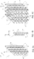
- FIG 1A illustrates a portion of a PCM memory (in the following referred to as "PCM block” 1) in a triaxial system of mutually orthogonal axes X, Y, Z.
- Figure 1B shows the PCM block 1 of Figure 1A in the XZ plane.
- Figure 1C shows a portion 1' of a PCM memory including a plurality of PCM blocks 1.
- the PCM block 1 is manufactured by processing a substrate of a silicon wafer through front-end processing steps, in particular manufacturing steps of a CMOS process.
- insulation regions not illustrated in Figure 1A ), which delimit active areas.
- Formed (e.g., by implants of dopant species) in the active areas are drain regions, source regions, and gate regions of respective MOS transistors 15.
- the PCM block 1 further includes a plurality of contacts 11 (e.g., of tungsten) having the function of electrical contacts with the aforementioned MOS transistors 15. Each contact 11 extends with electrical continuity in the direction of the Z axis.
- the MOS transistors 15 are also referred to as selection transistors, operable to address, during use, memory cells of PCM block 1.
- the contacts 11 extend, in one embodiment, in the form of pillars.
- phase-change material elements for example a chalcogenide such as a GST (Ge-Sb-Te) compound, in particular Ge 2 Sb 2 Te 5 extend in a strip-like form along a respective direction parallel to the Y-axis; each PCM element 50 is thermally and electrically separated (or isolated) from the other PCM elements 50.
- chalcogenide such as a GST (Ge-Sb-Te) compound, in particular Ge 2 Sb 2 Te 5
- GST GST
- Ge 2 Sb 2 Te 5 Ge 2 Sb 2 Te 5
- FIG 2 is a schematic electrical illustration of Figure 1B (showing one column 11 to which resistive regions 34 and PCM elements 50 are coupled).
- one end of each of the resistive regions 34 is in electrical contact with a respective portion of one contact 11; the other end of each resistive region 34 is electrically coupled to an electrical terminal of a respective control switch M1, M2, ..., MN (switches are not shown in Figures 1A-1C ) through a portion of the phase-change material (PCM element 50).
- the other electrical terminal of each control switch M1-MN is connected to a biasing voltage V DD .
- Each control switch M1-MN is, for example, a MOS transistor and the electrical terminals are source and drain terminals.
- the gate terminal of each control switch M1-MN can be biased by a respective control signal Vb1-VbN provided by a respective control line, to turn on/off the respective control switch M1-MN.
- PCM element 50 The portion of the PCM element 50 directly coupled to one respective resistive region 34, and such resistive region 34, form a PCM cell, which can be programmed (in logic states known as SET and RESET) and read to write and, respectively, acquire a logic datum stored in the phase-change memory element.
- a writing (programming) operation by activating (i.e., turning on) a control switch M1, M2, ..., MN and the selector transistor 15 to which the respective contact 11 is coupled, an electrical current flows through the PCM cell, to cause the respective resistive region 34 to generate heat by Joule effect.
- the PCM cell is biased at a writing voltage by applying a voltage V DD across it.
- the PCM element 50 is coupled to each resistive region 34 in a per se known way, to receive the heat generated through Joule effect by the resistive region 34.
- the electrical resistance of the contact 11 (in the range of few ⁇ , or few tens of ⁇ ) is negligible with respect to the resistance of the resistive region (heater) 34 (in the range of some k ⁇ , or few tens of k ⁇ ). Accordingly, the programming voltage drops almost completely across the resistive region 34.
- SET and RESET pulses are shown; during a time interval T1 a RESET pulse is generated, that is an electric pulse adapted to program the addressed PCM cells in the logic state "0". Similarly, during a time interval T2, a SET pulse is generated, that is an electric pulse adapted to program the addressed PCM cells in the logic state "1".
- the SET and RESET pulses are known to have different shapes both in terms of duration in time and in maximum voltage/current values.
- the RESET voltage pulse has a duration T1 lower than the duration T2 of the SET pulse; however, the maximum voltage value V1 (or corresponding current value) needed for the RESET pulse is higher than the maximum voltage value V2 (or corresponding current value) needed for the SET pulse.
- V1 3V
- V3 ⁇ 1V equal to 0.6V during a reading operation
- V1 Vreset according to the technology and design parametrs
- V2 is chosen equal to 2/3 ⁇ Vreset and V3 is chosen lower than, or equal to, 1/3 ⁇ Vreset (in any case, lower than the "RESET” threshold).
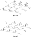
- Figures 4A, 4B show a simplified electrical representation of one PCM block 1 of the PCM memory 1';
- Figures 5A , 5B show a simplified electrical representation of a plurality of PCM blocks 1.
- each line r1-r3 corresponds to a respective stripe of PCM element 50 to be biased
- each line c1-c3 corresponds to the biasing lines used to bias the gate terminals of selection transistors 15 belonging to different PCM blocks 1 and aligned along the X-axis.
- Figures 4A, 4B and 5A , 5B show only three lines r1-r3 and three lines c1-c3; it is apparent that the teaching applies to any number of lines.
- PCM cells are connected between lines r1-r3 and lines c1-c3, forming a matrix.
- the present invention foresees a double writing step.
- Figures 4A and 5A show the voltage distribution during a first writing step aimed at writing (i.e., program) the PCM cells connected to the same line r2.
- Lines c2 and c3 are biased at the intermediate voltage of 1V, so that the voltage drop across all the other PCM cells is 0V or 1V and, in any case, in a voltage range that do not alter the already programmed state of such cells. In this situation, a spurious power consumption exists, but is the limited to the size of the PCM block 1 considered.
- the required voltage values for the columns 11 can be obtained by biasing the gate terminals of the selection transistors 15 using lines c1-c3 and use the threshold voltage drop to have the required voltage on the respective contacts 11.
- the other PCB block that are not currently programmed are not stressed (all their lines are biased at 0V).
- Figure 6 shows graphically a possible reading scheme, according to a schematic representation of a PCM memory having a matrix-like arrangement of rows and columns, and PCM cells coupled between such rows and columns. Only the addressed PCM cells are read, while all the others are not stressed, i.e. voltage applied to the PCM cells not to be read is zero.
- Sense amplifiers 16 carry out reading of the data stored in the PCM cells, comparing the current that flows in the PCM cell selected (or an electrical quantity correlated thereto) with a reference current that flows in a reference cell (so-called double-ended reading) or else with a reference current supplied by a reference-current generator (so-called single-ended reading).
- each line c1-c3 and r1-r3 is connected to a respective transistor the connects / disconnects such line to / from the biasing voltage.
- all of these transistors are not equivalent in term of size (they are designed according to the maximum voltage/current they must sustain during use).
- a current is needed to flow through the transistors associated to the lines r1-r3, thus implementing a write operation "by row” and allowing the corresponding transistors to sink only the current related to the single PCM cell to be written.
- the sense amplifiers 16 should not be connected "by row", because, as shown in Figure 6 , line r2 "sees" the total current of all PCM cells connected to it.
- a wafer 100 including a semiconductor body 102 (including a substrate and, optionally, one or more epitaxial layers on the substrate, for example of silicon).
- a semiconductor body 102 including a substrate and, optionally, one or more epitaxial layers on the substrate, for example of silicon.
- a plurality of selection transistors 15 are formed in the semiconductor body 102.
- the selection transistors 15 defines active areas of semiconductor body 102.
- a dielectric or insulating layer 104 is formed over the semiconductor body 102, e.g. by growing or depositing silicon oxide or silicon nitride.
- trenches are formed within the dielectric layer 104, reaching and exposing the conductive terminals of the selection transistors 15.
- a conductive material e.g., metal
- LIL local interconnection lines
- plugs 106 that are in electrical contact with the selection transistors 15 (in particular with a conductive terminal, such as the drain terminal) of the selection transistors 15.
- the plugs 106 connect the selection transistors 15 to further conductive layers that will be formed above the dielectric layer 104 (such as the contacts 11) .
- a step of deposition a resistive layer for example doped titanium nitride (doped-TiN) is carried out on the dielectric layer 104 and the plugs 106.
- This step is followed by formation, in a per se known manner, of a layer of phase-change material, for example by depositing a chalcogenide, such as a GST (Ge-Sb-Te) compound, e.g., Ge 2 Sb 2 Te 5 .
- a chalcogenide such as a GST (Ge-Sb-Te) compound, e.g., Ge 2 Sb 2 Te 5 .
- Other phase-change materials may be used.
- Formation of the PCM layer is carried out over the resistive layer.
- the resistive layer and the PCM layer thus formed are patterned, e.g. through lithography and etching, to form a stack including the resistive region 34 and the PCM element 50 previously described, having a shape and an extension according to the design of the PCM memory 1'.
- the PM element 50 is a continuous strip along Y-axis, while the resistive regions 34 extend at selective regions of the PCM element 50, i.e. at the regions of the PCM element 50 that are designed to form a memory cell. Between one resistive region 34 and another resistive region 34, along the Y-axis extension of the PM element 50, dielectric or insulating material can be deposited.
- a protective layer 110 e.g. of silicon nitride, is formed on the resistive region 34 and the PCM element 50.
- the protective layer 110 may also extend over the dielectric layer 104 and the portions of the plugs 106 not covered by the resistive layer 34.
- a step is carried out to deposit and pattern a metal layer 118 over the dielectric layer 112.
- the metal layer 118 is patterned in such a way to define a plurality of local interconnections 118', each of them being electrically connected to one respective plug 116.
- a dielectric or insulating layer 121 is formed analogously to the dielectric layer 112 and further metal interconnections 122 (analogous to metal interconnections 118') are formed on the dielectric layer 121.
- Figure 12 illustrates a portion of a system 200 that may be implemented in various devices, such as for example PDAs, portable computers, phones, photographic cameras, video cameras, etc.
- the system 200 may include one or more among a controller 210 (e.g., a microprocessor), an input/output device 220, for example a keypad and a display, a chip housing in an integrated form the PCM memory 1', a wireless interface 240, and a random-access memory (RAM) 260, connected together by a bus system 250.
- the system 200 may be supplied by a battery 280, or alternatively by a mains supply source. It is clear that the scope of the present disclosure is not limited to embodiments comprising all the components of Figure 12 .
- the random-access memory (RAM) 260, the wireless interface 240, the battery 280, and the input/output device 220 may be omitted.
- the area/bit of a PCM memory according to the present invention is considerably reduced with respect to known PCM memories.
- the increase of the level also increases the area gain depending of the number of the cells stacked.
Landscapes
- Chemical & Material Sciences (AREA)
- Crystallography & Structural Chemistry (AREA)
- Engineering & Computer Science (AREA)
- Manufacturing & Machinery (AREA)
- Semiconductor Memories (AREA)
- Design And Manufacture Of Integrated Circuits (AREA)
- Logic Circuits (AREA)
Abstract
Description
- The present invention relates to a phase-change memory (PCM) block, a phase-change memory including a plurality of PCM blocks, a method for manufacturing the PCM block and methods for programming and reading the PCM block. In particular, the PCM block is of a physical multilevel type.
- As is known, phase-change memories use a class of materials having the property of switching between two phases having distinct electrical characteristics, associated to two different crystallographic structures of the material, and precisely a non-orderly amorphous phase and an orderly crystalline or polycrystalline phase. The two phases are thus associated to values of resistivity that differ considerably from one another, even by two or more orders of magnitude.
- Currently, the elements of Group XVI of the periodic table, such as for example Te or Se, also known as chalcogenide materials or chalcogenides, may be used in phase-change memory cells. As is known, for example, from P. Zuliani, et al., "Overcoming Temperature Limitations in Phase Change Memories With Optimized GexSbyTez", IEEE Transactions on Electron Devices, Volume 60, Issue 12, pages 4020-4026, Nov. 1, 2013, it is possible to use alloys of Ge, Sb, and Te (GexSbyTez, for example Ge2Sb2Te5) optimised by appropriately choosing the percentages of the elements that form said alloys.
- The temperature at which phase transition occurs depends upon the phase-change material used. In the case of Ge2Sb2Te5 alloy, for example, below 150°C both the amorphous phase and the crystalline phase are stable. If the temperature is increased beyond 200°C, there is noted a fast re-arrangement of the crystals, and the material becomes crystalline. To bring the chalcogenide into the amorphous state, it is necessary to increase further the temperature up to melting point (approximately 600°C) and then cool it rapidly.
- Numerous memories are known that exploit phase-change materials as elements for storage of the two stable states (amorphous and crystalline states), which may each be associated to a respective bit at "1" or at "0". In these memories, a plurality of memory cells are arranged in rows and columns to form an array. Each memory cell is coupled to a respective selection element, which may be implemented by any switching device, such as PN diodes, bipolar junction transistors, or MOS transistors, and typically includes a chalcogenide region in contact with a resistive contact, also known as heater. A storage element is formed in a contact area between the chalcogenide region and the heater. The heater is connected to a conduction terminal of the selection element.
- From an electrical standpoint, the crystallization temperature and the melting temperature are obtained by causing flow of an electric current through the resistive contact that extends in direct contact with or is functionally coupled to the chalcogenide material, thus heating it by the Joule effect.
- According to the prior art, various processes of production of phase-change memory cells are known, which, however, present some disadvantages and limitations. In particular, in PCM of know type, each storage element is typically configured to store one bit only. To overcome this limitation, multilevel storage elements have been proposed, wherein one cell can be programmed according to more than two resistance values, so that a respective plurality of information can be stored in the cell. The plurality of resistance values can be achieved by using controlled writing pulses that can set intermediate resistance states between the "SET" state and the "RESET" state.
- The stability of the intermediate levels of the resistance is a critical aspect due to the drift in resistance values in time and temperature.
- There is thus felt the need to provide a phase-change memory (PCM) block, a phase-change memory including a plurality of PCM blocks, a method for manufacturing the PCM block and methods for programming and reading the PCM block, that meet the need identified above.
- Patent document
US2010/259962 relates to structure, use and making of re-programmable non-volatile memory cell arrays, and, more specifically, to three-dimensional arrays of memory storage elements formed on semiconductor substrates. - Patent document
US2010/270593 relates to high density memory devices, and particularly to memory devices in which multiple planes of memory cells are arranged to provide a three-dimensional 3D array. - Patent document
US2013/170283 relates to technology for non-volatile storage. - However, the above-mentioned drawbacks are not overcome.
- According to the present invention, a phase-change memory (PCM) block, a phase-change memory including a plurality of PCM blocks, a method for manufacturing the PCM block and methods for programming and reading the PCM block are consequently provided, as defined in the annexed claims.
- For a better understanding of the present invention, preferred embodiments thereof are now described, purely by way of non-limiting example and with reference to the attached drawings, wherein:
-
Figures 1A and 1B show respective views of a PCM block according to the present invention; -
Figure 1C shows a PCM memory including a plurality of PCM blocks ofFigure 1B ; -
Figure 2 is a schematic electrical representation of the PCM block ofFigure 1B ; -
Figure 3 sows SET and RESET pulses to be applied to a PCM cell in order to program the PCM cell in respective logic states; -
Figures 4A, 4B show schematically a circuit representation of one PCM block ofFigure 1A , with an exemplary biasing scheme for programming the PCM block; -
Figures 5A ,5B show schematically a circuit representation of a PCM memory ofFigure 1C including a plurality of PCM blocks, with an exemplary biasing scheme method for programming the PCM memory; -
Figure 6 shows schematically a circuit representation of one PCM block ofFigure 1A , with an exemplary biasing scheme for reading the PCM block; -
Figures 7-11 show subsequent method steps to manufacture a PCM block ofFigure 1A ; -
Figure 12 schematically shows a system that includes one or more PCM blocks ofFigure 1A or 1B , or a PCM memory ofFigure 1C ; and -
Figure 13 is a further embodiment of a PCM block. -
Figure 1A illustrates a portion of a PCM memory (in the following referred to as "PCM block" 1) in a triaxial system of mutually orthogonal axes X, Y, Z.Figure 1B shows thePCM block 1 ofFigure 1A in the XZ plane.Figure 1C shows a portion 1' of a PCM memory including a plurality ofPCM blocks 1. - The
PCM block 1 is manufactured by processing a substrate of a silicon wafer through front-end processing steps, in particular manufacturing steps of a CMOS process. In particular, formed in the substrate are insulation regions (not illustrated inFigure 1A ), which delimit active areas. Formed (e.g., by implants of dopant species) in the active areas are drain regions, source regions, and gate regions ofrespective MOS transistors 15. - The
PCM block 1 further includes a plurality of contacts 11 (e.g., of tungsten) having the function of electrical contacts with theaforementioned MOS transistors 15. Eachcontact 11 extends with electrical continuity in the direction of the Z axis. TheMOS transistors 15 are also referred to as selection transistors, operable to address, during use, memory cells ofPCM block 1. - With reference to
Figure 1A , thecontacts 11 extend, in one embodiment, in the form of pillars. - A plurality of phase-change material elements (in what follows, "PCM element") 50, for example a chalcogenide such as a GST (Ge-Sb-Te) compound, in particular Ge2Sb2Te5 extend in a strip-like form along a respective direction parallel to the Y-axis; each
PCM element 50 is thermally and electrically separated (or isolated) from theother PCM elements 50. - A plurality of resistive regions 34 (i.e., heaters, having the function of locally heating the
PCM element 50 for triggering a selective phase-change of the heated portion) are further present. With reference toFigure 1B , a plurality ofresistive regions 34 extend laterally to eachcontact 11. Considering onecontact 11, eachresistive region 34 of such plurality ofresistive regions 34 arranged laterally to the consideredcontact 11, has one end electrically coupled to thatcontact 11 and the other end electrically and thermally coupled to a portion of thePCM element 50 designed to store a logic datum (i.e., designed to undergo a phase-change of SET or RESET type). In other words, a plurality (two or more) ofresistive regions 34 are electrically coupled to eachcontact 11. More in particular, for eachcontact 11, theresistive regions 34 are coupled between thatcontact 11 and arespective PCM element 50. -
Figure 2 is a schematic electrical illustration ofFigure 1B (showing onecolumn 11 to whichresistive regions 34 andPCM elements 50 are coupled). With further reference toFigure 2 , one end of each of theresistive regions 34 is in electrical contact with a respective portion of onecontact 11; the other end of eachresistive region 34 is electrically coupled to an electrical terminal of a respective control switch M1, M2, ..., MN (switches are not shown inFigures 1A-1C ) through a portion of the phase-change material (PCM element 50). The other electrical terminal of each control switch M1-MN is connected to a biasing voltage VDD. (Each control switch M1-MN is, for example, a MOS transistor and the electrical terminals are source and drain terminals. The gate terminal of each control switch M1-MN can be biased by a respective control signal Vb1-VbN provided by a respective control line, to turn on/off the respective control switch M1-MN. - The portion of the
PCM element 50 directly coupled to one respectiveresistive region 34, and suchresistive region 34, form a PCM cell, which can be programmed (in logic states known as SET and RESET) and read to write and, respectively, acquire a logic datum stored in the phase-change memory element. - During a writing (programming) operation, by activating (i.e., turning on) a control switch M1, M2, ..., MN and the
selector transistor 15 to which therespective contact 11 is coupled, an electrical current flows through the PCM cell, to cause the respectiveresistive region 34 to generate heat by Joule effect. During use, to program a SET or RESET state of the memory element, the PCM cell is biased at a writing voltage by applying a voltage VDD across it. ThePCM element 50 is coupled to eachresistive region 34 in a per se known way, to receive the heat generated through Joule effect by theresistive region 34. - The electrical resistance of the contact 11 (in the range of few Ω, or few tens of Ω) is negligible with respect to the resistance of the resistive region (heater) 34 (in the range of some kΩ, or few tens of kΩ). Accordingly, the programming voltage drops almost completely across the
resistive region 34. - With reference to
Figure 3 , SET and RESET pulses are shown; during a time interval T1 a RESET pulse is generated, that is an electric pulse adapted to program the addressed PCM cells in the logic state "0". Similarly, during a time interval T2, a SET pulse is generated, that is an electric pulse adapted to program the addressed PCM cells in the logic state "1". The SET and RESET pulses are known to have different shapes both in terms of duration in time and in maximum voltage/current values. In particular, the RESET voltage pulse has a duration T1 lower than the duration T2 of the SET pulse; however, the maximum voltage value V1 (or corresponding current value) needed for the RESET pulse is higher than the maximum voltage value V2 (or corresponding current value) needed for the SET pulse. In the present description, the voltage value to be applied to thePCM element 50 to program the RESET state is considered to be V1=3V; the voltage value to be applied to thePCM element 50 to program the SET state is considered to be V2=2V; the voltage value to be applied to thePCM element 50 not to change the already programmed state is considered to be V3<1V (equal to 0.6V during a reading operation). It is apparent that these values are not limiting the present invention, and are used in the following disclosure for merely improving the understanding of the present invention. Of course, other voltage values can be used depending upon the specific design of the memory, the phase-change material used, etc. In general terms, provided that V1=Vreset according to the technology and design parametrs, V2 is chosen equal to 2/3·Vreset and V3 is chosen lower than, or equal to, 1/3·Vreset (in any case, lower than the "RESET" threshold). - Writing or programming operations of the
PCM block 1 and PCM memory 1' are described with reference toFigures 4A, 4B and5A ,5B .Figures 4A, 4B show a simplified electrical representation of onePCM block 1 of the PCM memory 1';Figures 5A ,5B show a simplified electrical representation of a plurality of PCM blocks 1. - In
figures 4A, 4B and5A ,5B , each line r1-r3 corresponds to a respective stripe ofPCM element 50 to be biased, and each line c1-c3 corresponds to the biasing lines used to bias the gate terminals ofselection transistors 15 belonging todifferent PCM blocks 1 and aligned along the X-axis. For ease of representation,Figures 4A, 4B and5A ,5B show only three lines r1-r3 and three lines c1-c3; it is apparent that the teaching applies to any number of lines. - PCM cells are connected between lines r1-r3 and lines c1-c3, forming a matrix. To program the PCM cells, the present invention foresees a double writing step.
-
Figures 4A and5A show the voltage distribution during a first writing step aimed at writing (i.e., program) the PCM cells connected to the same line r2. During this operation, all the cells in the addressed line r2 are written to the "RESET" or "0" state (i.e., by applying a pulse of V1=3V across them), irrespective of whether such PCM cells are to be programmed at the RESET state or the SET state. To this end, line r2 is biased at a reference voltage of 0V (e.g., ground), while lines r1 and r3 are biased at V1=3V. In order to have the required voltage drop across the PCM cell to be programmed, all lines c1-c3 are biased at V1=3V. Therefore, only the PCM cells coupled to r2 undergoes a voltage drop of 3V, while the PCM cells coupled to r1 and r3 undergoes a voltage drop of 0V. Consequently, the PCM cell coupled between r2 and c1-c3 are all programmed at the RESET state, while the remaining PCM cells retain their current state. - In a second writing step,
Figures 4B and5B , carried out after the first writing step, the SET pulse is applied selectively to those PCM cells coupled to the line r2 that are to be programmed at the SET state, while maintaining unaltered the already programmed RESET state in those PCM cells that are to be programmed at the RESET state. To this end, line r2 is biased at the reference potential of 0V, while lines r1 and r3 are biased at an intermediate voltage of 1V. - It is supposed in this example that only the PCM cell coupled between r2 and c1 is to be programmed at the SET state. Therefore, line c1 is biased at V2=2V, so that the voltage drop across the PCM cell coupled between r2 and c1 is V2=2V, and the PCM cell is programmed at the SET state.
- Lines c2 and c3 are biased at the intermediate voltage of 1V, so that the voltage drop across all the other PCM cells is 0V or 1V and, in any case, in a voltage range that do not alter the already programmed state of such cells. In this situation, a spurious power consumption exists, but is the limited to the size of the
PCM block 1 considered. - With specific reference to
Figures 5A and5B , it can be appreciated that the required voltage values for thecolumns 11 can be obtained by biasing the gate terminals of theselection transistors 15 using lines c1-c3 and use the threshold voltage drop to have the required voltage on therespective contacts 11. The gate terminals are, in this example, biased at 4V and, with a threshold supposed to be equal to 1V, one can have V1=3V on therespective contact 11. It is noted, as represented inFigures 5A and5B , that the other PCB block that are not currently programmed are not stressed (all their lines are biased at 0V). -
Figure 6 shows graphically a possible reading scheme, according to a schematic representation of a PCM memory having a matrix-like arrangement of rows and columns, and PCM cells coupled between such rows and columns. Only the addressed PCM cells are read, while all the others are not stressed, i.e. voltage applied to the PCM cells not to be read is zero. - Line r2, to which the PCM cells to be read are coupled, is biased at reference voltage of 0V, while all other lines r1 and r3 are biased at V3=0.6V. All lines c1-c3 are biased at V3=0.6V. Therefore, a voltage drop of V3=0.6V is applied only across the PCM cells coupled between line r2 and lines c1-c3; the remaining PCM cells are subject to a null voltage drop. It is therefore apparent that during the reading operations there is no spurious current consumption. The actual reading operation is performed through
sense amplifiers 16, in a per se known way.Sense amplifiers 16 carry out reading of the data stored in the PCM cells, comparing the current that flows in the PCM cell selected (or an electrical quantity correlated thereto) with a reference current that flows in a reference cell (so-called double-ended reading) or else with a reference current supplied by a reference-current generator (so-called single-ended reading). - It is noted that each line c1-c3 and r1-r3 is connected to a respective transistor the connects / disconnects such line to / from the biasing voltage. In practice all of these transistors are not equivalent in term of size (they are designed according to the maximum voltage/current they must sustain during use). To perform the write operation, a current is needed to flow through the transistors associated to the lines r1-r3, thus implementing a write operation "by row" and allowing the corresponding transistors to sink only the current related to the single PCM cell to be written. During reading, the
sense amplifiers 16 should not be connected "by row", because, as shown inFigure 6 , line r2 "sees" the total current of all PCM cells connected to it. Taking the above into account, a solution is to write "by row" and read "by column", that is to say connect thesense amplifiers 16 to the lines c1-c3 during reading operations, to read the current flowing through the line r2, which is the only line selected for reading. Since the matrix shown inFigure 6 is symmetric, the comparators may be connected to the lines r1-r3 as well, to perform the reading operation.Figures 5A and5B shown a 3D representation of the matrix; in this case, the comparators must be connected to the lines r1-r3 to perform a reading operation. In any case, it is noted that the currently known method for reading a PCM memory can be applied analogously to the PCM memory according to the present application. - With reference to
Figures 7-11 , a method for manufacturing the PCM memory 1' is disclosed, according to an embodiment of the present invention. - With reference to
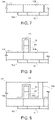
Figure 7 , a wafer 100 is provided, including a semiconductor body 102 (including a substrate and, optionally, one or more epitaxial layers on the substrate, for example of silicon). By known techniques, for example belonging to a standard CMOS process, a plurality ofselection transistors 15 are formed in thesemiconductor body 102. Theselection transistors 15 defines active areas ofsemiconductor body 102. A dielectric or insulatinglayer 104 is formed over thesemiconductor body 102, e.g. by growing or depositing silicon oxide or silicon nitride. - Through a lithographic step, trenches are formed within the
dielectric layer 104, reaching and exposing the conductive terminals of theselection transistors 15. A conductive material (e.g., metal) is deposited within the trenches thus forming respective local interconnection lines, LIL, or plugs 106 that are in electrical contact with the selection transistors 15 (in particular with a conductive terminal, such as the drain terminal) of theselection transistors 15. Theplugs 106 connect theselection transistors 15 to further conductive layers that will be formed above the dielectric layer 104 (such as the contacts 11) . - Then,
Figure 8 , steps are carried out to form the resistive regions 34 (heaters) and thePCM elements 50. To this end, a step of deposition a resistive layer, for example doped titanium nitride (doped-TiN), is carried out on thedielectric layer 104 and theplugs 106. This step is followed by formation, in a per se known manner, of a layer of phase-change material, for example by depositing a chalcogenide, such as a GST (Ge-Sb-Te) compound, e.g., Ge2Sb2Te5. Other phase-change materials may be used. Formation of the PCM layer is carried out over the resistive layer. - The resistive layer and the PCM layer thus formed are patterned, e.g. through lithography and etching, to form a stack including the
resistive region 34 and thePCM element 50 previously described, having a shape and an extension according to the design of the PCM memory 1'. It is noted that thePM element 50 is a continuous strip along Y-axis, while theresistive regions 34 extend at selective regions of thePCM element 50, i.e. at the regions of thePCM element 50 that are designed to form a memory cell. Between oneresistive region 34 and anotherresistive region 34, along the Y-axis extension of thePM element 50, dielectric or insulating material can be deposited. - A
protective layer 110, e.g. of silicon nitride, is formed on theresistive region 34 and thePCM element 50. Theprotective layer 110 may also extend over thedielectric layer 104 and the portions of theplugs 106 not covered by theresistive layer 34. - Then,
Figure 9 , a further dielectric or insulatinglayer 112 is formed (e.g., deposited) over theresistive region 34, thePCM element 50, theprotective layer 110, thedielectric layer 104 and theplugs 106. A CMP ("Chemical-Mechanical-Polishing") step on the isdielectric layer 112 carried out. Trenches are opened through thedielectric layer 112 and theprotective layer 110, reaching a region of theplugs 106 lateral to the stack formed by theresistive region 34 and thePM layer 50. The trenches are then filled with conductive material, in particular metal, more in particular tungsten.Plugs 116 extending entirely through thedielectric layer 112, in electrical contact withrespective plugs 106 are thus formed. - Then,
Figure 10 , a step is carried out to deposit and pattern ametal layer 118 over thedielectric layer 112. Themetal layer 118 is patterned in such a way to define a plurality of local interconnections 118', each of them being electrically connected to onerespective plug 116. - The structure of
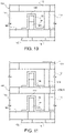
Figure 10 (with the exception of the formation oftransistors 15 and plugs 106) is then replicated, as shown inFigure 11 . - With reference to
Figure 11 , the steps previously described are repeated in order to form further stacks ofresistive regions 34 andPCM elements 50 and further plugs 120 (analogous toplugs 116 previously described) above the local interconnections 118' and in electrical contact with respective local interconnections 118'. A dielectric or insulatinglayer 121 is formed analogously to thedielectric layer 112 and further metal interconnections 122 (analogous to metal interconnections 118') are formed on thedielectric layer 121. - In particular, the stack identified with
reference numeral 128 inFigure 11 , including theplug 106 extending in electrical contact with oneselection transistor 15, theplug 116 extending in electrical contact withsuch plug 106, the metal interconnection 118' extending in electrical contact withsuch plug 116, thefurther plug 120 and thefurther metal interconnection 122 extending in electrical contact with suchfurther plug 120 form (at least in part) onecontact 11 previously described. A plurality overPCM elements 50, each one including therespective heaters 34, extend one above the other along the Z-axis and are electrically connected to the same stack 128 (contact 11), as in the embodiments ofFigures 1A-1C . - The steps of
Figure 11 can be replicated as many time as desired, according to the design of the PCM memory 1'. -
Figure 12 illustrates a portion of a system 200 that may be implemented in various devices, such as for example PDAs, portable computers, phones, photographic cameras, video cameras, etc. The system 200 may include one or more among a controller 210 (e.g., a microprocessor), an input/output device 220, for example a keypad and a display, a chip housing in an integrated form the PCM memory 1', awireless interface 240, and a random-access memory (RAM) 260, connected together by a bus system 250. According to one embodiment, the system 200 may be supplied by abattery 280, or alternatively by a mains supply source. It is clear that the scope of the present disclosure is not limited to embodiments comprising all the components ofFigure 12 . For example, one or more from among the random-access memory (RAM) 260, thewireless interface 240, thebattery 280, and the input/output device 220 may be omitted. - The advantages of the present disclosure emerge clearly from the foregoing description.
- For example, the area/bit of a PCM memory according to the present invention is considerably reduced with respect to known PCM memories. The increase of the level also increases the area gain depending of the number of the cells stacked.
- Finally, it is clear that modifications and variations may be made to what has been described and illustrated herein, without thereby departing from the scope of the present invention, as defined in the annexed claims.
- For example,
Figure 13 shown a PCM block 300 according to a further embodiment of the present invention. Elements of the PCM block 300 common to thePCM block 1 ofFigure 1B are identified with the same reference numerals. As shown inFigure 13 , further resistive regions (heaters) 34' extend away from thecontact 11 at a side of thecontact 11 opposite to the side facing theresistive regions 34. Resistive regions 34' have characteristics analogous to theresistive regions 34, and are manufactured accordingly during the same process steps, in a way that is per se apparent to the skilled person.PCM elements 50 are electrically and thermally coupled to the resistive regions 34', analogously toPCM elements 50. The functioning of the PCM block 300 is the same as that ofPCM block 1 and is therefore not further described.
Claims (23)
- A phase-change memory, PCM, block (1), comprising:a semiconductor body (102) housing a selection transistor (15);a electrical-insulation body (112, 121) on the semiconductor body (102);a conductive region (11), extending through the electrical-insulation body (112, 121), electrically coupled to the selection transistor (15);a plurality of heater elements (34) in the electrical-insulation body (112, 121), each including a first end in electrical contact with a respective portion of the conductive region (11) and a second end that extends away from the conductive region (11); anda plurality of phase-change elements (50) extending in the electrical-insulation body (112, 121) and including data storage regions, each data storage region being electrically and thermally coupled to one respective heater element (34) at the second end of the respective heater element (34).
- The PCM block according to claim 1, wherein said electrical-insulation body (112, 121) includes a plurality of overlying electrical-insulation layers (112, 121), each heater element (34) and the associated data-storage region (50) extending in a respective one of said electrical-insulation layers (112; 121).
- The PCM block according to claim 2, wherein said conductive region (11) includes a plurality of electrically interconnected plugs (116, 120), each plug extending in a respective one of said electrical-insulation layers (112; 121) .
- The PCM block according to claim 2 or 3, wherein said plurality of electrical-insulation layers (112; 121) includes one or more stacks of overlying electrical-insulation layers (112; 121), each stack including a respective first electrical-insulation layer (121) on a respective second electrical-insulation layer (112),and wherein for each stack a respective interconnection conductive line (118') extends between said first (112) and second (121) electrical-insulation layers,the interconnection conductive line (118') being electrically connected to the plug extending in said first electrical-insulation layer (112) and to the plug extending in said second electrical-insulation layer (121) thus forming a conductive path between the first and the second electrical-insulation layers (112, 121).
- The PCM block according to claim 4, wherein said interconnection conductive line (118') is further electrically connected to the heater element (34) extending in the first electrical-insulation layer (121).
- The PCM block according to anyone of the preceding claims, wherein each heater element (34) and the data-storage region (50) coupled to it are covered by a sealing layer (110) of dielectric or insulating material.
- The PCM block according to anyone of the preceding claims, wherein said heater elements (34) are aligned to one another along a vertical direction (Z) orthogonal to a plane of lie (XY) of said substrate (102).
- The PCM block according to anyone of the preceding claims, wherein the conductive region (11) has a main extension along a first direction (Z) orthogonal to a plane of lie (XY) of the substrate (102), each heater element (34) being arranged laterally to the conductive region (11).
- The PCM block according to any one of the preceding claims, further comprising a plurality of switching transistors (M1-MN), each one having an own first conduction terminal coupled to one respective phase-change element (50), an own second conduction terminal coupled to a bias potential (VDD) and an own control terminal,wherein the selection transistor (15) includes an own first conduction terminal coupled to the conductive region (11), an own second conduction terminal coupled to a reference-potential (GND), and an own control terminal,the control terminals of the selection transistor (15) and of the switching transistors (M1-MN) being operable to selectively connect one respective heater element (34) and the associated phase-change element (50) between the reference-potential (GND) and the bias potential (VDD).
- The PCM block according to any one of the preceding claims, wherein the conductive region (11) has a value of electrical resistance negligible with respect to the electrical resistance of each heater element (34).
- A phase-change memory (1'), including a plurality of PCM blocks (1) according to anyone of claims 1-10.
- A chip comprising:- one or more PCM blocks (1) according to anyone of claims 1-10;- a biasing circuitry comprising:a programming stage including voltage generators configured to cause a SET or RESET programming current to flow through selected heater elements (34) to generate heath by Joule effect, so as to cause a controlled phase-transition of the associated data-storage region of the phase-change element (50);a reading stage including a plurality of sense amplifiers (16), each coupled to one respective data-storage region (50) to read a current flowing through the respective data-storage region (50) during a read operation of the PCM block (1).
- A system (200) comprising:
a processing unit (210); and one among:at least one PCM block (1) according to anyone of claims 1-10;a phase-change memory (1') according to claim 11;a chip according to claim 12. - A method of manufacturing a phase-change memory, PCM, block (1), comprising the steps of:forming, in a semiconductor body (102), a selection transistor (15);forming an electrical-insulation body (112, 121) on the semiconductor body (102);forming a conductive region (11) through the electrical-insulation body (112, 121), electrically coupled to the selection transistor (15);forming a plurality of heater elements (34) in the electrical-insulation body (112, 121), each including a first end in electrical contact with a respective portion of the conductive region (11) and a second end that extends away from the conductive region (11); andforming a plurality of phase-change elements (50) extending in the electrical-insulation body (112, 121) and including data-storage regions, each data-storage region being electrically and thermally coupled to one respective heater element (34) at the second end of the respective heater element (34).
- The method according to claim 14, wherein forming said electrical-insulation body (112, 121) includes forming a plurality of overlying electrical-insulation layers (112, 121), and wherein forming the heater elements (34) and the data-storage region (50) includes burying each heater element (34) and the associated data-storage region (50) in a respective one of said electrical-insulation layers (112; 121) .
- The method according to claim 15, wherein forming the conductive region (11) includes forming a plug in a respective one of said electrical-insulation layers (112; 121) and electrically connecting each of said plugs to one another.
- The method according to claim 15 or 16, wherein forming said plurality of electrical-insulation layers (112; 121) includes forming one or more stacks of overlying electrical-insulation layers (112; 121), each stack including a respective first electrical-insulation layer (121) on a respective second electrical-insulation layer (112),the method further comprising forming, for each stack, a respective interconnection conductive line (118') between said first (112) and second (121) electrical-insulation layers,the interconnection conductive line (118') being formed in electrical connection with the plug extending in said first electrical-insulation layer (112) and with the plug extending in said second electrical-insulation layer (121) thus forming a conductive path between the first and the second electrical-insulation layers (112, 121).
- The method according to claim 17, wherein said interconnection conductive line (118') is further electrically connected to the heater element (34) extending in the first electrical-insulation layer (121).
- The method according to anyone of claims 14-18, further comprising the step of forming a sealing layer (110) of dielectric or insulating material covering a respective heater element (34) and data-storage region (50) coupled to that heater element (34).
- The method according to anyone of claims 14-19, wherein said heater elements (34) are formed aligned to one another along a vertical direction (Z) orthogonal to a plane of lie (XY) of said substrate (102).
- The method according to anyone of claims 14-20, wherein the conductive region (11) is formed with a main extension along a first direction (Z) orthogonal to a plane of lie (XY) of the substrate (102), each heater element (34) being formed laterally to the conductive region (11).
- A method for programming a phase-change memory (1'), said phase-change memory device (1) comprising:at least one row line (r2);a plurality of column line (c1-c3);a plurality of phase-change memory cells, each of them being coupled between the row line (r2) and one respective column line (c1-c3);the method comprising the steps of:in a first operating condition associated with a first time interval (T1), applying a RESET programming voltage to the plurality of phase-change memory cells, thus programming said plurality of phase-change memory cells to a first logic state; andin a second operating condition associated with a second time interval (T2) that is subsequent to the first time interval (T1), applying a SET programming voltage to selected phase-change memory cells among said plurality of phase-change memory cells, thus programming said selected phase-change memory cells to a second logic state,wherein the maximum voltage value of the RESET programming voltage is higher than that of the SET programming voltage.
- A method for reading a phase-change memory (1'), said phase-change memory device (1) comprising:a plurality of row lines (r1-r3);a plurality of column line (c1-c3);a plurality of phase-change memory cells, each of them being coupled between the row line (r2) and one respective column line (c1-c3);the method comprising the steps of:bias one row line to which a phase-change memory cell to be read is connected, among said plurality of row lines, at a ground reference voltage;bias the remaining row line of said plurality of row lines at a reading voltage;bias the plurality of column line (c1-c3) at said reading voltage;acquire, through a sense amplifier (16), a current flowing through the column line (c1-c3) to which the phase-change memory cells to be read is connected.
Applications Claiming Priority (1)
| Application Number | Priority Date | Filing Date | Title |
|---|---|---|---|
| IT102020000032270A IT202000032270A1 (en) | 2020-12-23 | 2020-12-23 | MULTILEVEL PHASE CHANGE MEMORY, METHOD FOR MANUFACTURING MULTILEVEL PHASE CHANGE MEMORY, AND METHODS FOR PROGRAMMING AND READING MULTILEVEL PHASE CHANGE MEMORY |
Publications (1)
| Publication Number | Publication Date |
|---|---|
| EP4020571A1 true EP4020571A1 (en) | 2022-06-29 |
Family
ID=74858692
Family Applications (1)
| Application Number | Title | Priority Date | Filing Date |
|---|---|---|---|
| EP21217194.6A Withdrawn EP4020571A1 (en) | 2020-12-23 | 2021-12-22 | Multilevel phase-change memory, method for manufacturing the multilevel phase-change memory and methods for programming and reading the multilevel phase-change memory |
Country Status (4)
| Country | Link |
|---|---|
| US (2) | US12120967B2 (en) |
| EP (1) | EP4020571A1 (en) |
| CN (2) | CN114664881B (en) |
| IT (1) | IT202000032270A1 (en) |
Families Citing this family (1)
| Publication number | Priority date | Publication date | Assignee | Title |
|---|---|---|---|---|
| IT202000032270A1 (en) * | 2020-12-23 | 2022-06-23 | St Microelectronics Srl | MULTILEVEL PHASE CHANGE MEMORY, METHOD FOR MANUFACTURING MULTILEVEL PHASE CHANGE MEMORY, AND METHODS FOR PROGRAMMING AND READING MULTILEVEL PHASE CHANGE MEMORY |
Citations (3)
| Publication number | Priority date | Publication date | Assignee | Title |
|---|---|---|---|---|
| US20100259962A1 (en) | 2009-04-08 | 2010-10-14 | Tianhong Yan | Three-Dimensional Array of Re-Programmable Non-Volatile Memory Elements Having Vertical Bit Lines and a Single-Sided Word Line Architecture |
| US20100270593A1 (en) | 2009-04-27 | 2010-10-28 | Macronix International Co., Ltd. | Integrated circuit 3d memory array and manufacturing method |
| US20130170283A1 (en) | 2011-12-30 | 2013-07-04 | Sandisk 3D Llc | Low forming voltage non-volatile storage device |
Family Cites Families (24)
| Publication number | Priority date | Publication date | Assignee | Title |
|---|---|---|---|---|
| US6646902B2 (en) * | 2001-08-30 | 2003-11-11 | Micron Technology, Inc. | Method of retaining memory state in a programmable conductor RAM |
| US6687147B2 (en) * | 2002-04-02 | 2004-02-03 | Hewlett-Packard Development Company, L.P. | Cubic memory array with diagonal select lines |
| KR100448893B1 (en) * | 2002-08-23 | 2004-09-16 | 삼성전자주식회사 | Phase-changeable memory device and method for fabricating the same |
| US20050158950A1 (en) * | 2002-12-19 | 2005-07-21 | Matrix Semiconductor, Inc. | Non-volatile memory cell comprising a dielectric layer and a phase change material in series |
| US6937507B2 (en) * | 2003-12-05 | 2005-08-30 | Silicon Storage Technology, Inc. | Memory device and method of operating same |
| US7307268B2 (en) * | 2005-01-19 | 2007-12-11 | Sandisk Corporation | Structure and method for biasing phase change memory array for reliable writing |
| JP4427464B2 (en) * | 2005-02-02 | 2010-03-10 | シャープ株式会社 | Nonvolatile semiconductor memory device and operation method thereof |
| JP4890016B2 (en) * | 2005-03-16 | 2012-03-07 | ルネサスエレクトロニクス株式会社 | Nonvolatile semiconductor memory device |
| TWI264087B (en) * | 2005-12-21 | 2006-10-11 | Ind Tech Res Inst | Phase change memory cell and fabricating method thereof |
| US7345899B2 (en) * | 2006-04-07 | 2008-03-18 | Infineon Technologies Ag | Memory having storage locations within a common volume of phase change material |
| JP5539610B2 (en) * | 2007-03-02 | 2014-07-02 | ピーエスフォー ルクスコ エスエイアールエル | Phase change memory programming and reading methods |
| US7869257B2 (en) * | 2007-12-17 | 2011-01-11 | Qimonda Ag | Integrated circuit including diode memory cells |
| US7791057B2 (en) | 2008-04-22 | 2010-09-07 | Macronix International Co., Ltd. | Memory cell having a buried phase change region and method for fabricating the same |
| KR101069724B1 (en) * | 2009-12-22 | 2011-10-04 | 주식회사 하이닉스반도체 | Phase Change Memory Having 3 Dimension Stack Structure and Method of Manufacturing the Same |
| JP5713942B2 (en) * | 2012-03-16 | 2015-05-07 | 株式会社東芝 | Variable resistance nonvolatile semiconductor memory device |
| US20130336053A1 (en) * | 2012-04-24 | 2013-12-19 | Being Advanced Memory Corporation | Paralleled Drive Devices Per Bitline in Phase-Change Memory Array |
| US8841649B2 (en) * | 2012-08-31 | 2014-09-23 | Micron Technology, Inc. | Three dimensional memory array architecture |
| US8964442B2 (en) * | 2013-01-14 | 2015-02-24 | Macronix International Co., Ltd. | Integrated circuit 3D phase change memory array and manufacturing method |
| US10147876B1 (en) * | 2017-08-31 | 2018-12-04 | Sandisk Technologies Llc | Phase change memory electrode with multiple thermal interfaces |
| US10374014B2 (en) * | 2017-10-16 | 2019-08-06 | Sandisk Technologies Llc | Multi-state phase change memory device with vertical cross-point structure |
| WO2019118931A1 (en) * | 2017-12-16 | 2019-06-20 | Hsu Fu Chang | 3d vertical memory array cell structures with individual selectors and processes |
| US10650889B1 (en) * | 2018-12-14 | 2020-05-12 | Samsung Electronics Co., Ltd. | Energy efficient phase change random access memory cell array write via controller-side aggregation management |
| US11985909B2 (en) * | 2019-06-10 | 2024-05-14 | Intel Corporation | Fabrication of stackable embedded eDRAM using a binary alloy based on antimony |
| IT202000032270A1 (en) * | 2020-12-23 | 2022-06-23 | St Microelectronics Srl | MULTILEVEL PHASE CHANGE MEMORY, METHOD FOR MANUFACTURING MULTILEVEL PHASE CHANGE MEMORY, AND METHODS FOR PROGRAMMING AND READING MULTILEVEL PHASE CHANGE MEMORY |
-
2020
- 2020-12-23 IT IT102020000032270A patent/IT202000032270A1/en unknown
-
2021
- 2021-12-17 US US17/644,942 patent/US12120967B2/en active Active
- 2021-12-22 CN CN202111582592.9A patent/CN114664881B/en active Active
- 2021-12-22 EP EP21217194.6A patent/EP4020571A1/en not_active Withdrawn
- 2021-12-22 CN CN202123248333.0U patent/CN217562572U/en active Active
-
2024
- 2024-09-13 US US18/884,913 patent/US20250008847A1/en active Pending
Patent Citations (3)
| Publication number | Priority date | Publication date | Assignee | Title |
|---|---|---|---|---|
| US20100259962A1 (en) | 2009-04-08 | 2010-10-14 | Tianhong Yan | Three-Dimensional Array of Re-Programmable Non-Volatile Memory Elements Having Vertical Bit Lines and a Single-Sided Word Line Architecture |
| US20100270593A1 (en) | 2009-04-27 | 2010-10-28 | Macronix International Co., Ltd. | Integrated circuit 3d memory array and manufacturing method |
| US20130170283A1 (en) | 2011-12-30 | 2013-07-04 | Sandisk 3D Llc | Low forming voltage non-volatile storage device |
Non-Patent Citations (1)
| Title |
|---|
| P. ZULIANI ET AL.: "Overcoming Temperature Limitations in Phase Change Memories With Optimized Ge Sb Te", IEEE TRANSACTIONS ON ELECTRON DEVICES, vol. 60, 1 November 2013 (2013-11-01), pages 4020 - 4026 |
Also Published As
| Publication number | Publication date |
|---|---|
| IT202000032270A1 (en) | 2022-06-23 |
| US12120967B2 (en) | 2024-10-15 |
| US20250008847A1 (en) | 2025-01-02 |
| US20220199900A1 (en) | 2022-06-23 |
| CN217562572U (en) | 2022-10-11 |
| CN114664881B (en) | 2025-08-26 |
| CN114664881A (en) | 2022-06-24 |
Similar Documents
| Publication | Publication Date | Title |
|---|---|---|
| US10879459B2 (en) | Phase change memory cell with constriction structure | |
| TWI492433B (en) | Reversible programmable resistive memory and providing method, phase change memory, electronic system | |
| US7422926B2 (en) | Self-aligned process for manufacturing phase change memory cells | |
| TWI452680B (en) | Phase-change memory, electronics system, reversible resistive memory and method for providing the same | |
| KR100796430B1 (en) | Phase change access device for memory | |
| US6567293B1 (en) | Single level metal memory cell using chalcogenide cladding | |
| CN101872838B (en) | Memory cell with buried phase change region and manufacturing method thereof | |
| US20040051128A1 (en) | Method to enhance performance of thermal resistor device | |
| US20100061132A1 (en) | Semiconductor storage device | |
| US8445880B2 (en) | Phase change memory device having bit-line discharge block and method of fabricating the same | |
| US20120181499A1 (en) | QUATERNARY GALLIUM TELLURIUM ANTIMONY (M-GaTeSb) BASED PHASE CHANGE MEMORY DEVICES | |
| TWI550621B (en) | Circuit and system of using junction diode as program selector for electrical fuses with extended area for one-time programmable devices | |
| US20250008847A1 (en) | Phase-change memory including phase-change elements in series with respective heater elements and methods for manufacturing, programming, and reading thereof | |
| US20060071244A1 (en) | Switching or amplifier device, in particular transistor | |
| US8927957B2 (en) | Sidewall diode driving device and memory using same | |
| CN106133841B (en) | One-time programmable memory, electronic system, method for operating one-time programmable memory and method for programming one-time programmable memory | |
| CN103871464A (en) | Programmable resistance element memory, operation method and electronic system | |
| EP4352791B1 (en) | 3d stackable bidirectional access device for a memory array | |
| US20240422992A1 (en) | Memory circuit comprising electronic cells and a control circuit |
Legal Events
| Date | Code | Title | Description |
|---|---|---|---|
| PUAI | Public reference made under article 153(3) epc to a published international application that has entered the european phase |
Free format text: ORIGINAL CODE: 0009012 |
|
| STAA | Information on the status of an ep patent application or granted ep patent |
Free format text: STATUS: THE APPLICATION HAS BEEN PUBLISHED |
|
| AK | Designated contracting states |
Kind code of ref document: A1 Designated state(s): AL AT BE BG CH CY CZ DE DK EE ES FI FR GB GR HR HU IE IS IT LI LT LU LV MC MK MT NL NO PL PT RO RS SE SI SK SM TR |
|
| STAA | Information on the status of an ep patent application or granted ep patent |
Free format text: STATUS: REQUEST FOR EXAMINATION WAS MADE |
|
| 17P | Request for examination filed |
Effective date: 20221219 |
|
| RBV | Designated contracting states (corrected) |
Designated state(s): AL AT BE BG CH CY CZ DE DK EE ES FI FR GB GR HR HU IE IS IT LI LT LU LV MC MK MT NL NO PL PT RO RS SE SI SK SM TR |
|
| STAA | Information on the status of an ep patent application or granted ep patent |
Free format text: STATUS: EXAMINATION IS IN PROGRESS |
|
| 17Q | First examination report despatched |
Effective date: 20240508 |
|
| REG | Reference to a national code |
Ref country code: DE Ref legal event code: R079 Free format text: PREVIOUS MAIN CLASS: H01L0027240000 Ipc: H10B0063100000 |
|
| STAA | Information on the status of an ep patent application or granted ep patent |
Free format text: STATUS: THE APPLICATION HAS BEEN WITHDRAWN |
|
| RIC1 | Information provided on ipc code assigned before grant |
Ipc: H10B 63/10 20230101AFI20251121BHEP Ipc: H10N 70/20 20230101ALI20251121BHEP Ipc: H10N 70/00 20230101ALI20251121BHEP Ipc: H10B 63/00 20230101ALI20251121BHEP |
|
| 18W | Application withdrawn |
Effective date: 20251201 |