EP4020440A1 - Display device - Google Patents
Display device Download PDFInfo
- Publication number
- EP4020440A1 EP4020440A1 EP21207660.8A EP21207660A EP4020440A1 EP 4020440 A1 EP4020440 A1 EP 4020440A1 EP 21207660 A EP21207660 A EP 21207660A EP 4020440 A1 EP4020440 A1 EP 4020440A1
- Authority
- EP
- European Patent Office
- Prior art keywords
- voltage
- line
- display device
- disposed
- demux circuit
- Prior art date
- Legal status (The legal status is an assumption and is not a legal conclusion. Google has not performed a legal analysis and makes no representation as to the accuracy of the status listed.)
- Pending
Links
- 239000000758 substrate Substances 0.000 claims abstract description 41
- 230000005540 biological transmission Effects 0.000 claims description 40
- 239000010410 layer Substances 0.000 description 75
- 239000011229 interlayer Substances 0.000 description 42
- 208000036252 interstitial lung disease 1 Diseases 0.000 description 19
- 238000010586 diagram Methods 0.000 description 16
- 208000036971 interstitial lung disease 2 Diseases 0.000 description 16
- 239000011810 insulating material Substances 0.000 description 12
- 239000003990 capacitor Substances 0.000 description 5
- 101001078158 Homo sapiens Integrin alpha-1 Proteins 0.000 description 3
- 102100025323 Integrin alpha-1 Human genes 0.000 description 3
- 229910052581 Si3N4 Inorganic materials 0.000 description 3
- VYPSYNLAJGMNEJ-UHFFFAOYSA-N Silicium dioxide Chemical compound O=[Si]=O VYPSYNLAJGMNEJ-UHFFFAOYSA-N 0.000 description 3
- XUIMIQQOPSSXEZ-UHFFFAOYSA-N Silicon Chemical compound [Si] XUIMIQQOPSSXEZ-UHFFFAOYSA-N 0.000 description 3
- 229910052710 silicon Inorganic materials 0.000 description 3
- 239000010703 silicon Substances 0.000 description 3
- HQVNEWCFYHHQES-UHFFFAOYSA-N silicon nitride Chemical compound N12[Si]34N5[Si]62N3[Si]51N64 HQVNEWCFYHHQES-UHFFFAOYSA-N 0.000 description 3
- 229910052814 silicon oxide Inorganic materials 0.000 description 3
- 239000011521 glass Substances 0.000 description 2
- 238000004519 manufacturing process Methods 0.000 description 2
- 239000011159 matrix material Substances 0.000 description 2
- 230000004888 barrier function Effects 0.000 description 1
- 239000004973 liquid crystal related substance Substances 0.000 description 1
- 238000000034 method Methods 0.000 description 1
- 239000002096 quantum dot Substances 0.000 description 1
- 230000003252 repetitive effect Effects 0.000 description 1
Images





Classifications
-
- G—PHYSICS
- G09—EDUCATION; CRYPTOGRAPHY; DISPLAY; ADVERTISING; SEALS
- G09G—ARRANGEMENTS OR CIRCUITS FOR CONTROL OF INDICATING DEVICES USING STATIC MEANS TO PRESENT VARIABLE INFORMATION
- G09G3/00—Control arrangements or circuits, of interest only in connection with visual indicators other than cathode-ray tubes
- G09G3/20—Control arrangements or circuits, of interest only in connection with visual indicators other than cathode-ray tubes for presentation of an assembly of a number of characters, e.g. a page, by composing the assembly by combination of individual elements arranged in a matrix no fixed position being assigned to or needed to be assigned to the individual characters or partial characters
- G09G3/22—Control arrangements or circuits, of interest only in connection with visual indicators other than cathode-ray tubes for presentation of an assembly of a number of characters, e.g. a page, by composing the assembly by combination of individual elements arranged in a matrix no fixed position being assigned to or needed to be assigned to the individual characters or partial characters using controlled light sources
- G09G3/30—Control arrangements or circuits, of interest only in connection with visual indicators other than cathode-ray tubes for presentation of an assembly of a number of characters, e.g. a page, by composing the assembly by combination of individual elements arranged in a matrix no fixed position being assigned to or needed to be assigned to the individual characters or partial characters using controlled light sources using electroluminescent panels
- G09G3/32—Control arrangements or circuits, of interest only in connection with visual indicators other than cathode-ray tubes for presentation of an assembly of a number of characters, e.g. a page, by composing the assembly by combination of individual elements arranged in a matrix no fixed position being assigned to or needed to be assigned to the individual characters or partial characters using controlled light sources using electroluminescent panels semiconductive, e.g. using light-emitting diodes [LED]
- G09G3/3208—Control arrangements or circuits, of interest only in connection with visual indicators other than cathode-ray tubes for presentation of an assembly of a number of characters, e.g. a page, by composing the assembly by combination of individual elements arranged in a matrix no fixed position being assigned to or needed to be assigned to the individual characters or partial characters using controlled light sources using electroluminescent panels semiconductive, e.g. using light-emitting diodes [LED] organic, e.g. using organic light-emitting diodes [OLED]
- G09G3/3225—Control arrangements or circuits, of interest only in connection with visual indicators other than cathode-ray tubes for presentation of an assembly of a number of characters, e.g. a page, by composing the assembly by combination of individual elements arranged in a matrix no fixed position being assigned to or needed to be assigned to the individual characters or partial characters using controlled light sources using electroluminescent panels semiconductive, e.g. using light-emitting diodes [LED] organic, e.g. using organic light-emitting diodes [OLED] using an active matrix
- G09G3/3233—Control arrangements or circuits, of interest only in connection with visual indicators other than cathode-ray tubes for presentation of an assembly of a number of characters, e.g. a page, by composing the assembly by combination of individual elements arranged in a matrix no fixed position being assigned to or needed to be assigned to the individual characters or partial characters using controlled light sources using electroluminescent panels semiconductive, e.g. using light-emitting diodes [LED] organic, e.g. using organic light-emitting diodes [OLED] using an active matrix with pixel circuitry controlling the current through the light-emitting element
-
- G—PHYSICS
- G09—EDUCATION; CRYPTOGRAPHY; DISPLAY; ADVERTISING; SEALS
- G09G—ARRANGEMENTS OR CIRCUITS FOR CONTROL OF INDICATING DEVICES USING STATIC MEANS TO PRESENT VARIABLE INFORMATION
- G09G3/00—Control arrangements or circuits, of interest only in connection with visual indicators other than cathode-ray tubes
- G09G3/20—Control arrangements or circuits, of interest only in connection with visual indicators other than cathode-ray tubes for presentation of an assembly of a number of characters, e.g. a page, by composing the assembly by combination of individual elements arranged in a matrix no fixed position being assigned to or needed to be assigned to the individual characters or partial characters
- G09G3/22—Control arrangements or circuits, of interest only in connection with visual indicators other than cathode-ray tubes for presentation of an assembly of a number of characters, e.g. a page, by composing the assembly by combination of individual elements arranged in a matrix no fixed position being assigned to or needed to be assigned to the individual characters or partial characters using controlled light sources
- G09G3/30—Control arrangements or circuits, of interest only in connection with visual indicators other than cathode-ray tubes for presentation of an assembly of a number of characters, e.g. a page, by composing the assembly by combination of individual elements arranged in a matrix no fixed position being assigned to or needed to be assigned to the individual characters or partial characters using controlled light sources using electroluminescent panels
-
- H—ELECTRICITY
- H10—SEMICONDUCTOR DEVICES; ELECTRIC SOLID-STATE DEVICES NOT OTHERWISE PROVIDED FOR
- H10K—ORGANIC ELECTRIC SOLID-STATE DEVICES
- H10K59/00—Integrated devices, or assemblies of multiple devices, comprising at least one organic light-emitting element covered by group H10K50/00
- H10K59/10—OLED displays
- H10K59/12—Active-matrix OLED [AMOLED] displays
-
- G—PHYSICS
- G09—EDUCATION; CRYPTOGRAPHY; DISPLAY; ADVERTISING; SEALS
- G09F—DISPLAYING; ADVERTISING; SIGNS; LABELS OR NAME-PLATES; SEALS
- G09F9/00—Indicating arrangements for variable information in which the information is built-up on a support by selection or combination of individual elements
- G09F9/30—Indicating arrangements for variable information in which the information is built-up on a support by selection or combination of individual elements in which the desired character or characters are formed by combining individual elements
-
- G—PHYSICS
- G09—EDUCATION; CRYPTOGRAPHY; DISPLAY; ADVERTISING; SEALS
- G09G—ARRANGEMENTS OR CIRCUITS FOR CONTROL OF INDICATING DEVICES USING STATIC MEANS TO PRESENT VARIABLE INFORMATION
- G09G3/00—Control arrangements or circuits, of interest only in connection with visual indicators other than cathode-ray tubes
- G09G3/20—Control arrangements or circuits, of interest only in connection with visual indicators other than cathode-ray tubes for presentation of an assembly of a number of characters, e.g. a page, by composing the assembly by combination of individual elements arranged in a matrix no fixed position being assigned to or needed to be assigned to the individual characters or partial characters
-
- G—PHYSICS
- G09—EDUCATION; CRYPTOGRAPHY; DISPLAY; ADVERTISING; SEALS
- G09G—ARRANGEMENTS OR CIRCUITS FOR CONTROL OF INDICATING DEVICES USING STATIC MEANS TO PRESENT VARIABLE INFORMATION
- G09G3/00—Control arrangements or circuits, of interest only in connection with visual indicators other than cathode-ray tubes
- G09G3/20—Control arrangements or circuits, of interest only in connection with visual indicators other than cathode-ray tubes for presentation of an assembly of a number of characters, e.g. a page, by composing the assembly by combination of individual elements arranged in a matrix no fixed position being assigned to or needed to be assigned to the individual characters or partial characters
- G09G3/22—Control arrangements or circuits, of interest only in connection with visual indicators other than cathode-ray tubes for presentation of an assembly of a number of characters, e.g. a page, by composing the assembly by combination of individual elements arranged in a matrix no fixed position being assigned to or needed to be assigned to the individual characters or partial characters using controlled light sources
- G09G3/30—Control arrangements or circuits, of interest only in connection with visual indicators other than cathode-ray tubes for presentation of an assembly of a number of characters, e.g. a page, by composing the assembly by combination of individual elements arranged in a matrix no fixed position being assigned to or needed to be assigned to the individual characters or partial characters using controlled light sources using electroluminescent panels
- G09G3/32—Control arrangements or circuits, of interest only in connection with visual indicators other than cathode-ray tubes for presentation of an assembly of a number of characters, e.g. a page, by composing the assembly by combination of individual elements arranged in a matrix no fixed position being assigned to or needed to be assigned to the individual characters or partial characters using controlled light sources using electroluminescent panels semiconductive, e.g. using light-emitting diodes [LED]
- G09G3/3208—Control arrangements or circuits, of interest only in connection with visual indicators other than cathode-ray tubes for presentation of an assembly of a number of characters, e.g. a page, by composing the assembly by combination of individual elements arranged in a matrix no fixed position being assigned to or needed to be assigned to the individual characters or partial characters using controlled light sources using electroluminescent panels semiconductive, e.g. using light-emitting diodes [LED] organic, e.g. using organic light-emitting diodes [OLED]
-
- G—PHYSICS
- G09—EDUCATION; CRYPTOGRAPHY; DISPLAY; ADVERTISING; SEALS
- G09G—ARRANGEMENTS OR CIRCUITS FOR CONTROL OF INDICATING DEVICES USING STATIC MEANS TO PRESENT VARIABLE INFORMATION
- G09G3/00—Control arrangements or circuits, of interest only in connection with visual indicators other than cathode-ray tubes
- G09G3/20—Control arrangements or circuits, of interest only in connection with visual indicators other than cathode-ray tubes for presentation of an assembly of a number of characters, e.g. a page, by composing the assembly by combination of individual elements arranged in a matrix no fixed position being assigned to or needed to be assigned to the individual characters or partial characters
- G09G3/22—Control arrangements or circuits, of interest only in connection with visual indicators other than cathode-ray tubes for presentation of an assembly of a number of characters, e.g. a page, by composing the assembly by combination of individual elements arranged in a matrix no fixed position being assigned to or needed to be assigned to the individual characters or partial characters using controlled light sources
- G09G3/30—Control arrangements or circuits, of interest only in connection with visual indicators other than cathode-ray tubes for presentation of an assembly of a number of characters, e.g. a page, by composing the assembly by combination of individual elements arranged in a matrix no fixed position being assigned to or needed to be assigned to the individual characters or partial characters using controlled light sources using electroluminescent panels
- G09G3/32—Control arrangements or circuits, of interest only in connection with visual indicators other than cathode-ray tubes for presentation of an assembly of a number of characters, e.g. a page, by composing the assembly by combination of individual elements arranged in a matrix no fixed position being assigned to or needed to be assigned to the individual characters or partial characters using controlled light sources using electroluminescent panels semiconductive, e.g. using light-emitting diodes [LED]
- G09G3/3208—Control arrangements or circuits, of interest only in connection with visual indicators other than cathode-ray tubes for presentation of an assembly of a number of characters, e.g. a page, by composing the assembly by combination of individual elements arranged in a matrix no fixed position being assigned to or needed to be assigned to the individual characters or partial characters using controlled light sources using electroluminescent panels semiconductive, e.g. using light-emitting diodes [LED] organic, e.g. using organic light-emitting diodes [OLED]
- G09G3/3225—Control arrangements or circuits, of interest only in connection with visual indicators other than cathode-ray tubes for presentation of an assembly of a number of characters, e.g. a page, by composing the assembly by combination of individual elements arranged in a matrix no fixed position being assigned to or needed to be assigned to the individual characters or partial characters using controlled light sources using electroluminescent panels semiconductive, e.g. using light-emitting diodes [LED] organic, e.g. using organic light-emitting diodes [OLED] using an active matrix
-
- G—PHYSICS
- G09—EDUCATION; CRYPTOGRAPHY; DISPLAY; ADVERTISING; SEALS
- G09G—ARRANGEMENTS OR CIRCUITS FOR CONTROL OF INDICATING DEVICES USING STATIC MEANS TO PRESENT VARIABLE INFORMATION
- G09G3/00—Control arrangements or circuits, of interest only in connection with visual indicators other than cathode-ray tubes
- G09G3/20—Control arrangements or circuits, of interest only in connection with visual indicators other than cathode-ray tubes for presentation of an assembly of a number of characters, e.g. a page, by composing the assembly by combination of individual elements arranged in a matrix no fixed position being assigned to or needed to be assigned to the individual characters or partial characters
- G09G3/22—Control arrangements or circuits, of interest only in connection with visual indicators other than cathode-ray tubes for presentation of an assembly of a number of characters, e.g. a page, by composing the assembly by combination of individual elements arranged in a matrix no fixed position being assigned to or needed to be assigned to the individual characters or partial characters using controlled light sources
- G09G3/30—Control arrangements or circuits, of interest only in connection with visual indicators other than cathode-ray tubes for presentation of an assembly of a number of characters, e.g. a page, by composing the assembly by combination of individual elements arranged in a matrix no fixed position being assigned to or needed to be assigned to the individual characters or partial characters using controlled light sources using electroluminescent panels
- G09G3/32—Control arrangements or circuits, of interest only in connection with visual indicators other than cathode-ray tubes for presentation of an assembly of a number of characters, e.g. a page, by composing the assembly by combination of individual elements arranged in a matrix no fixed position being assigned to or needed to be assigned to the individual characters or partial characters using controlled light sources using electroluminescent panels semiconductive, e.g. using light-emitting diodes [LED]
- G09G3/3208—Control arrangements or circuits, of interest only in connection with visual indicators other than cathode-ray tubes for presentation of an assembly of a number of characters, e.g. a page, by composing the assembly by combination of individual elements arranged in a matrix no fixed position being assigned to or needed to be assigned to the individual characters or partial characters using controlled light sources using electroluminescent panels semiconductive, e.g. using light-emitting diodes [LED] organic, e.g. using organic light-emitting diodes [OLED]
- G09G3/3275—Details of drivers for data electrodes
-
- G—PHYSICS
- G09—EDUCATION; CRYPTOGRAPHY; DISPLAY; ADVERTISING; SEALS
- G09G—ARRANGEMENTS OR CIRCUITS FOR CONTROL OF INDICATING DEVICES USING STATIC MEANS TO PRESENT VARIABLE INFORMATION
- G09G3/00—Control arrangements or circuits, of interest only in connection with visual indicators other than cathode-ray tubes
- G09G3/20—Control arrangements or circuits, of interest only in connection with visual indicators other than cathode-ray tubes for presentation of an assembly of a number of characters, e.g. a page, by composing the assembly by combination of individual elements arranged in a matrix no fixed position being assigned to or needed to be assigned to the individual characters or partial characters
- G09G3/22—Control arrangements or circuits, of interest only in connection with visual indicators other than cathode-ray tubes for presentation of an assembly of a number of characters, e.g. a page, by composing the assembly by combination of individual elements arranged in a matrix no fixed position being assigned to or needed to be assigned to the individual characters or partial characters using controlled light sources
- G09G3/30—Control arrangements or circuits, of interest only in connection with visual indicators other than cathode-ray tubes for presentation of an assembly of a number of characters, e.g. a page, by composing the assembly by combination of individual elements arranged in a matrix no fixed position being assigned to or needed to be assigned to the individual characters or partial characters using controlled light sources using electroluminescent panels
- G09G3/32—Control arrangements or circuits, of interest only in connection with visual indicators other than cathode-ray tubes for presentation of an assembly of a number of characters, e.g. a page, by composing the assembly by combination of individual elements arranged in a matrix no fixed position being assigned to or needed to be assigned to the individual characters or partial characters using controlled light sources using electroluminescent panels semiconductive, e.g. using light-emitting diodes [LED]
- G09G3/3208—Control arrangements or circuits, of interest only in connection with visual indicators other than cathode-ray tubes for presentation of an assembly of a number of characters, e.g. a page, by composing the assembly by combination of individual elements arranged in a matrix no fixed position being assigned to or needed to be assigned to the individual characters or partial characters using controlled light sources using electroluminescent panels semiconductive, e.g. using light-emitting diodes [LED] organic, e.g. using organic light-emitting diodes [OLED]
- G09G3/3275—Details of drivers for data electrodes
- G09G3/3291—Details of drivers for data electrodes in which the data driver supplies a variable data voltage for setting the current through, or the voltage across, the light-emitting elements
-
- H—ELECTRICITY
- H10—SEMICONDUCTOR DEVICES; ELECTRIC SOLID-STATE DEVICES NOT OTHERWISE PROVIDED FOR
- H10K—ORGANIC ELECTRIC SOLID-STATE DEVICES
- H10K59/00—Integrated devices, or assemblies of multiple devices, comprising at least one organic light-emitting element covered by group H10K50/00
- H10K59/10—OLED displays
- H10K59/12—Active-matrix OLED [AMOLED] displays
- H10K59/128—Active-matrix OLED [AMOLED] displays comprising two independent displays, e.g. for emitting information from two major sides of the display
-
- H—ELECTRICITY
- H10—SEMICONDUCTOR DEVICES; ELECTRIC SOLID-STATE DEVICES NOT OTHERWISE PROVIDED FOR
- H10K—ORGANIC ELECTRIC SOLID-STATE DEVICES
- H10K59/00—Integrated devices, or assemblies of multiple devices, comprising at least one organic light-emitting element covered by group H10K50/00
- H10K59/10—OLED displays
- H10K59/12—Active-matrix OLED [AMOLED] displays
- H10K59/131—Interconnections, e.g. wiring lines or terminals
-
- G—PHYSICS
- G09—EDUCATION; CRYPTOGRAPHY; DISPLAY; ADVERTISING; SEALS
- G09G—ARRANGEMENTS OR CIRCUITS FOR CONTROL OF INDICATING DEVICES USING STATIC MEANS TO PRESENT VARIABLE INFORMATION
- G09G2300/00—Aspects of the constitution of display devices
- G09G2300/04—Structural and physical details of display devices
- G09G2300/0421—Structural details of the set of electrodes
- G09G2300/0426—Layout of electrodes and connections
-
- G—PHYSICS
- G09—EDUCATION; CRYPTOGRAPHY; DISPLAY; ADVERTISING; SEALS
- G09G—ARRANGEMENTS OR CIRCUITS FOR CONTROL OF INDICATING DEVICES USING STATIC MEANS TO PRESENT VARIABLE INFORMATION
- G09G2300/00—Aspects of the constitution of display devices
- G09G2300/08—Active matrix structure, i.e. with use of active elements, inclusive of non-linear two terminal elements, in the pixels together with light emitting or modulating elements
- G09G2300/0809—Several active elements per pixel in active matrix panels
- G09G2300/0842—Several active elements per pixel in active matrix panels forming a memory circuit, e.g. a dynamic memory with one capacitor
- G09G2300/0861—Several active elements per pixel in active matrix panels forming a memory circuit, e.g. a dynamic memory with one capacitor with additional control of the display period without amending the charge stored in a pixel memory, e.g. by means of additional select electrodes
-
- G—PHYSICS
- G09—EDUCATION; CRYPTOGRAPHY; DISPLAY; ADVERTISING; SEALS
- G09G—ARRANGEMENTS OR CIRCUITS FOR CONTROL OF INDICATING DEVICES USING STATIC MEANS TO PRESENT VARIABLE INFORMATION
- G09G2300/00—Aspects of the constitution of display devices
- G09G2300/08—Active matrix structure, i.e. with use of active elements, inclusive of non-linear two terminal elements, in the pixels together with light emitting or modulating elements
- G09G2300/0809—Several active elements per pixel in active matrix panels
- G09G2300/0842—Several active elements per pixel in active matrix panels forming a memory circuit, e.g. a dynamic memory with one capacitor
- G09G2300/0861—Several active elements per pixel in active matrix panels forming a memory circuit, e.g. a dynamic memory with one capacitor with additional control of the display period without amending the charge stored in a pixel memory, e.g. by means of additional select electrodes
- G09G2300/0866—Several active elements per pixel in active matrix panels forming a memory circuit, e.g. a dynamic memory with one capacitor with additional control of the display period without amending the charge stored in a pixel memory, e.g. by means of additional select electrodes by means of changes in the pixel supply voltage
-
- G—PHYSICS
- G09—EDUCATION; CRYPTOGRAPHY; DISPLAY; ADVERTISING; SEALS
- G09G—ARRANGEMENTS OR CIRCUITS FOR CONTROL OF INDICATING DEVICES USING STATIC MEANS TO PRESENT VARIABLE INFORMATION
- G09G2310/00—Command of the display device
- G09G2310/02—Addressing, scanning or driving the display screen or processing steps related thereto
- G09G2310/0264—Details of driving circuits
- G09G2310/0297—Special arrangements with multiplexing or demultiplexing of display data in the drivers for data electrodes, in a pre-processing circuitry delivering display data to said drivers or in the matrix panel, e.g. multiplexing plural data signals to one D/A converter or demultiplexing the D/A converter output to multiple columns
-
- G—PHYSICS
- G09—EDUCATION; CRYPTOGRAPHY; DISPLAY; ADVERTISING; SEALS
- G09G—ARRANGEMENTS OR CIRCUITS FOR CONTROL OF INDICATING DEVICES USING STATIC MEANS TO PRESENT VARIABLE INFORMATION
- G09G2320/00—Control of display operating conditions
- G09G2320/04—Maintaining the quality of display appearance
- G09G2320/043—Preventing or counteracting the effects of ageing
- G09G2320/045—Compensation of drifts in the characteristics of light emitting or modulating elements
-
- G—PHYSICS
- G09—EDUCATION; CRYPTOGRAPHY; DISPLAY; ADVERTISING; SEALS
- G09G—ARRANGEMENTS OR CIRCUITS FOR CONTROL OF INDICATING DEVICES USING STATIC MEANS TO PRESENT VARIABLE INFORMATION
- G09G2330/00—Aspects of power supply; Aspects of display protection and defect management
- G09G2330/02—Details of power systems and of start or stop of display operation
- G09G2330/028—Generation of voltages supplied to electrode drivers in a matrix display other than LCD
Definitions
- Embodiments relate to a display device, and particularly, a display device including a plurality of lines.
- the display device is manufactured in various types, including an organic light emitting display device, a liquid crystal display device, and a quantum-dot nano light emitting display device.
- the display device may have a shape such as a circle or a polygon.
- the display device may have a shape in which each vertex of a polygon has a curvature.
- a plurality of lines may be disposed in a non-display area of the display device.
- a low power voltage line, an initialization voltage line, a high power voltage line, and a data line may be disposed in a non-display area of a circular display device.
- a dead space may be formed by a space in which the low power voltage line, the initialization voltage line, the high power voltage line, and the data line are disposed.
- Embodiments provide a display device with reduced dead space.
- a display device includes a substrate on which a display area including a plurality of pixels and a non-display area surrounding the display area are defined, a first voltage line disposed on the substrate in the non-display area, where the first voltage line provides a first voltage to the pixels, a second voltage line disposed on the substrate in the non-display area, where the second voltage line provides a second voltage to the pixels, and a first demux circuit area and a second demux circuit area disposed on the substrate in the non-display area, where the first demux circuit area and the second demux circuit area transmit data signals to the pixels.
- the first voltage line passes an area between the first demux circuit area and the second demux circuit area.
- the display area may have a circular shape or another round shape, such as an elliptical shape, especially a curved or round shape without straight edges and vertexes.
- the display device may further include a first voltage bypass line connected to the first voltage line and disposed along an edge of the display area and a second voltage bypass line connected to the second voltage line and disposed along the edge of the display area.
- the first voltage may be an initialization voltage
- the second voltage may be a low power voltage
- the first voltage may be a low power voltage
- the second voltage may be an initialization voltage
- the first demux circuit area and the second demux circuit area may be disposed to be spaced apart in one direction.
- the one direction may be the longitudinal direction of a circuit board disposed on one side of the non-display area.
- the display device may further include a third voltage line disposed on the substrate in the non-display area, where the third voltage line may provide a third voltage to the pixels.
- the third voltage may be a high power voltage.
- a part of the third voltage line may pass the area between the first demux circuit area and the second demux circuit area.
- a width of the part of the third voltage line may be narrower than a width of another part of the third voltage line connected to the part.
- the display device may further include a plurality of voltage output lines connected to the first voltage line.
- some of the voltage output lines may partially overlap the first demux circuit area, and others of the voltage output lines except for the some partially may overlap the second demux circuit area.
- the display device may further include a voltage transmission line connected to the first voltage line.
- the voltage output lines may be connected to the first voltage line by the voltage transmission line.
- some of the voltage transmission lines may overlap the first demux circuit area, and others of the voltage transmission lines except for the some may overlap the second demux circuit area.
- the first voltage line and the voltage output line may be disposed in different layers from each other.
- the plurality of voltage output lines may be disposed in a same layer.
- At least some of the plurality of voltage output lines may be disposed in different layers from each other.
- the first demux circuit area may include a first demux circuit to which a first data signal is applied through a first data input line
- the second demux circuit area may include a second demux circuit to which a second data signal is applied through a second data input line
- the first data input line and the second data input line may be disposed in a same layer.
- the first data input line and the second data input line may be disposed in different layers from each other.
- the display device may further include a first data output line and a second data output line, which are connected to the first demux circuit and a third data output line and a fourth data output line, which are connected to the second demux circuit.
- the first to fourth data output lines may be disposed in a same layer.
- At least one selected from the first to fourth data output lines may be disposed in a different layer from another selected therefrom.
- the first voltage line may include a first part disposed between the first demux circuit and the second demux circuit, and a second part connected to the first part, and a width of the first part may be narrower than a width of the second part.
- the display device may include a substrate on which a display area including a plurality of pixels and a non-display area surrounding the display area are defined, a first voltage line disposed on the substrate in the non-display area to provide a first voltage to the pixels, a second voltage line disposed on the substrate in the non-display area to provide a second voltage to the pixels, and a first demux circuit area and a second demux circuit area disposed on the substrate in the non-display area to transmit data signals to the pixels.
- the first voltage line may pass an area between the first demux circuit area and the second demux circuit area.
- the non-display area at the lower end of the display device may be reduced compared to a case where the first voltage line is disposed to bypass a demux circuit area.
- relative terms such as “lower” or “bottom” and “upper” or “top,” may be used herein to describe one element's relationship to another element as illustrated in the Figures. It will be understood that relative terms are intended to encompass different orientations of the device in addition to the orientation depicted in the Figures. For example, if the device in one of the figures is turned over, elements described as being on the “lower” side of other elements would then be oriented on “upper” sides of the other elements. The term “lower,” can therefore, encompasses both an orientation of “lower” and “upper,” depending on the particular orientation of the figure.
- Embodiments are described herein with reference to cross section illustrations that are schematic illustrations of idealized embodiments. As such, variations from the shapes of the illustrations as a result, for example, of manufacturing techniques and/or tolerances, are to be expected. Thus, embodiments described herein should not be construed as limited to the particular shapes of regions as illustrated herein but are to include deviations in shapes that result, for example, from manufacturing. For example, a region illustrated or described as flat may, typically, have rough and/or nonlinear features. Moreover, sharp angles that are illustrated may be rounded. Thus, the regions illustrated in the figures are schematic in nature and their shapes are not intended to illustrate the precise shape of a region and are not intended to limit the scope of the present claims.
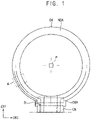
- FIG. 1 is a plan view illustrating a display device according to an embodiment
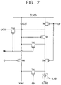
- FIG. 2 is a circuit diagram illustrating a pixel included in the display device of FIG. 1 .
- an embodiment of the display device may include a display area DA and a non-display area NDA surrounding the display area DA.
- the display area DA may have a curvature.
- the display area DA may have a circular shape having a constant curvature as a whole.
- the display area DA may include a part having a linear shape or a straight outer side, and another part having a shape having a curvature or a curved outer side.
- a plurality of pixels P may be disposed in the display area DA.
- the pixels P may be arranged in various shapes in the display area DA.
- the pixels P may be entirely arranged in a matrix form in the display area DA.
- the pixels P may be arranged in a matrix form in a central part of the display area DA, and may be arranged in a stepwise manner at a edge of the display area DA.
- the pixels P may be arranged in various shapes corresponding to a shape of the display area DA for displaying an image thereon.
- Each of the pixels P may include at least one transistor and at least one capacitor.
- FIG. 2 illustrates an embodiment of a pixel including seven transistors and a single capacitor.
- each of the pixels P may include first to seventh transistors TR1, TR2, TR3, TR4, TR5, TR6, TR7, and a storage capacitor CST, as shown in FIG. 2 .
- the display device may be an organic light emitting display device, and each of the pixels P may further include an organic light emitting diode OLED.
- each of the pixels P may include three transistors and a single capacitor. In such embodiments, each of the pixels P may include various numbers of transistors and capacitors for driving the pixels P.
- each of the pixels P may receive a data signal DATA, gate signals GW, GI, GB, an light emitting signal EM, a high power voltage ELVDD, a low power voltage ELVSS, and an initialization voltage VINT, but not being limited thereto.
- an additional voltage e.g., a compensation voltage
- the non-display area NDA may have a shape corresponding to the shape of the display area DA.
- the display area DA may have a circular shape
- the non-display area NDA may have a circular shape (or a circular band shape) having a same curvature as the display area DA.
- the non-display area NDA may have a shape independent from the display area DA.
- the display area DA may have a circular shape
- the non-display area NDA may have a polygonal shape.
- a plurality of demux circuits may be disposed on one side portion of the non-display area NDA.
- Each of the demux circuits may output the data signal DATA through a plurality of data output lines after receiving the data signal DATA from a data input line.
- the display device may efficiently utilize a space in which the lines are arranged in the non-display area NDA.
- the demux circuits may be disposed in a demux circuit area DXA.
- the demux circuit area DXA may be disposed adjacent to the display area DA.
- the demux circuit area DXA and the display area DA may be disposed adjacent to each other in a first direction DR1.
- the demux circuit area DXA may extend in a second direction DR2 perpendicular to the first direction DR1.
- the demux circuits may be arranged in parallel in the second direction DR2.
- the demux circuit area DXA may extend to correspond to the curvature of the display area DA.
- the demux circuits may be disposed along the edge of the display area DA.
- a circuit board CB may be disposed on one side of the non-display area NDA.
- the circuit board CB may transmit various signals and voltages to the pixels P.
- the circuit board CB may be disposed on or to overlap the non-display area NDA, or may be disposed to be connected to the non-display area NDA by a separate film.
- Lines extending from the circuit board CB may be connected to the display area DA after passing through the non-display area NDA.
- FIG. 1 shows only a portion of the lines for convenience of illustration, and the display device may include more lines.
- the lines may be entirely disposed along the edge of the display area DA, or may be disposed only in a part of the edge.
- FIG. 3 is a diagram illustrating an embodiment in which area A of the display device of FIG. 1 is enlarged.
- an embodiment of the display device may include a plurality of lines.
- some of the lines may be disposed along the edge of the display area DA.
- a first voltage bypass line VBL1 and a second voltage bypass line VBL2 may be disposed along the edge of the display area DA.
- each of the first voltage bypass line VBL1 and the second voltage bypass line VBL2 may have a curvature.
- Each of the first voltage bypass line VBL1 and the second voltage bypass line VBL2 may be connected to voltage lines to be described later.
- the first voltage bypass line VBL1 may be connected to the pixels P by a plurality of lines.
- the second voltage bypass line VBL2 may be connected to the pixels P by a plurality of lines.
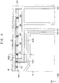
- FIG. 4 is a diagram illustrating an embodiment in which area B of the display device of FIG. 1 is enlarged.
- an embodiment of the display device may include a first voltage line VL1, a second voltage line VL2, a third voltage line VL3, a first voltage transmission line VC1, first to sixth voltage output lines VO1, VO2, VO3, VO4, VO5, VO6.
- the display device may include a first demux circuit area DXA1 and a second demux circuit area DXA2.
- a demux circuit e.g., one or more demux circuits
- a first voltage may be applied to the first voltage line VL1.
- the initialization voltage VINT may be applied to the first voltage line VL1 as the first voltage.
- the first voltage line VL1 may pass (or extend through) an area between the first demux circuit area DXA1 and the second demux circuit area DXA2.
- the first demux circuit area DXA1 and the second demux circuit area DXA2 may be spaced apart from each other by the first voltage line VL1.
- the term spaced apart from each other by a signal or voltage line means that the respective mentioned areas, especially circuit areas, are spaced apart from each other by a distance and the respective mentioned line is located in or protrudes through this distance.
- the first voltage line VL1 does not bypass the first demux circuit area DXA1, thereby reducing the non-display area NDA of the display device.
- the first voltage line VL1 may be connected to the first voltage transmission line VC1 through a contact hole.
- the first voltage transmission line VC1 may be connected to the first to sixth voltage output lines V01, VO2, VO3, VO4, VO5, VO6 through a contact hole, respectively.
- the initialization voltage VINT flowing through the first voltage line VL1 may be transferred to the pixels P through the first voltage transmission line VC1 and the first to sixth voltage output lines V01, VO2, VO3, VO4, VO5, VO6.
- the first voltage transmission line VC1 may be partially disposed to overlap the first demux circuit area DXA1 and the second demux circuit area DXA2.
- the first to sixth voltage output lines V01, VO2, VO3, VO4, VO5, VO6 may be partially disposed to overlap the first demux circuit area DXA1 and the second demux circuit area DXA2.
- the first to sixth voltage output lines V01, VO2, VO3, VO4, VO5, VO6 may pass an area between the demux circuits.
- the demux circuits and the first to sixth voltage output lines V01, VO2, VO3, VO4, VO5, VO6 may be disposed not to overlap each other.
- the first voltage transmission line VC1 and the first to sixth voltage output lines V01, VO2, VO3, VO4, VO5, VO6 may be disposed on different layers.
- the first voltage transmission line VC1 may be disposed above the first to sixth voltage output lines V01, VO2, VO3, VO4, VO5, VO6.
- the first voltage transfer line VC1 may be disposed below the first to sixth voltage output lines V01, VO2, VO3, VO4, VO5, and VO6.
- the first voltage transmission line VC1 may be connected to the first voltage bypass line VBL1.
- the first voltage transmission line VC1 may be integrally formed with the first voltage bypass line VBL1 as a single unitary unit.
- the first voltage transmission line VC1 may be connected to the first voltage bypass line VBL1 through a contact hole.
- the initialization voltage VINT may flow along the edge of the display area DA through the first voltage bypass line VBL1.
- the first voltage bypass line VBL1 may apply the initialization voltage VINT to the pixels P by lines connecting the first voltage bypass line VBL1 and the pixels P.
- the first voltage line VL1 may include a first part VLA1 disposed between the first demux circuit area DXA1 and the second demux circuit area DXA2, and a second part VLA2 connected to the first part VLA2.
- a width of the first part VLA1 may be narrower than a width of the second part VLA2.
- an area between the first demux circuit area DXA1 and the second demux circuit area DXA2 that are spaced apart from each other may be minimized.
- a second voltage different from the first voltage may be applied to the second voltage line VL2.
- the low power voltage ELVSS may be applied to the second voltage line VL2 as the second voltage.
- the second voltage line VL2 may be connected to the second voltage bypass line VBL2.
- the low power voltage ELVSS may flow along the edge of the display area DA through the second voltage bypass line VBL2.
- the second voltage bypass line VBL2 may apply the low power voltage ELVSS to the pixels P by lines connecting the second voltage bypass line VBL2 and the pixels P.
- the low power voltage ELVSS may be applied to the first voltage line VL1
- the initialization voltage VINT may be applied to the second voltage line VL2.
- the first voltage bypass line VBL1 may be connected to the first voltage line VL1 passing between the first demux circuit area DXA1 and the second demux circuit area DXA2, thereby reducing the non-display area NDA at the lower part of the display device.
- the non-display area NDA at the lower part of the display device may be reduced compared to a case where the first voltage line VL1 is turned to the outside of the demux circuit area DXA and is connected to the first voltage bypass line VBL1.
- a third voltage different from the first voltage and the second voltage may be applied to the third voltage line VL3.
- the high power voltage ELVDD may be applied to the third voltage line VL3 as the third voltage.
- the high power voltage ELVDD may be applied to the third voltage line VL3 by a plurality of input units.
- the third voltage line VL3 may be disposed to surround the second demux circuit area DXA2.
- the third voltage line VL3 may comprise several sections or parts which may be disposed to surround the second demux circuit area DXA2.
- a plurality of demux circuits may be disposed between the third voltage line VL3 or between the different sections or parts of the third voltage line VL3.
- the first demux circuit area DXA1 and the second demux circuit area DXA2 may be spaced apart from each other by the third voltage line VL3 or by a section or part of the third voltage line VL3.
- the third voltage line VL3 may provide the high power voltage ELVDD to the pixels P by a plurality of output units VP.
- the first demux circuit area DXA1 and the second demux circuit area DXA2 may be spaced apart by the third voltage line VL3 or by a section or part of the third voltage line VL3.
- a width of a first part of the third voltage line VL3 disposed between the first demux circuit area DXA1 and the second demux circuit area DXA2 may be narrower than a width of other part of the third voltage line VL3 connected to the first part, such that a space between the first demux circuit area DXA1 and the second demux circuit area DXA2, which are spaced apart from each other, may be minimized.
- the other part of the third voltage line VL3, which may be termed as a second part, may extend angular (with an angel other than 0° and 180°) or perpendicular to the first part.
- the third voltage line VL3 may comprise further parts parallel or angular (with an angel other than 0° and 180°) or perpendicular to the first part and/or second part.
- FIG. 5 is a diagram illustrating an embodiment in which area B of the display device of FIG. 1 is enlarged.
- FIG. 5 may be substantially the same as FIG. 4 except for lines to which the initialization voltage VINT is applied.
- the same or like elements shown in FIG. 5 have been labeled with the same reference characters as used above to describe the embodiment of the display device shown in FIG. 1 , and any repetitive detailed description thereof will hereinafter be omitted or simplified.
- the first voltage line VL1 may be directly connected to the first to fourth voltage output lines V01, VO2, VO3, VO4 through a contact hole.
- the first voltage line VL1 may be connected to the second voltage transmission line VC2 through a contact hole
- the fifth and sixth voltage output lines VO5, VO6 may be connected to the second voltage transmission line VC2 through a contact hole.
- the fifth and sixth voltage output lines VO5, VO6 may be connected to the first voltage line VL1 by the second voltage transmission line VC2.
- the second voltage transmission line VC2 may be disposed to be spaced apart from the second demux circuit area DXA2.
- the second voltage transmission line VC2 may not overlap the second demux circuit area DXA2.
- the first to sixth voltage output lines V01, VO2, VO3, VO4, VO5, VO6 may partially overlap the second demux circuit area DXA2.
- the first voltage line VL1 may be connected to the first bypass line VBL1.
- the first voltage line VL1 may be integrally formed with the first voltage bypass line VBL1 as a single unitary unit.
- the first voltage line VL1 may be connected to the first voltage bypass line VBL1 through a contact hole.
- the first voltage line VL1 passes an area between the first demux circuit area DXA1 and the second demux circuit area DXA2 and is connected to the first voltage bypass line VBL1, such that the area of the lower end of the non-display area NDA of the display device may be reduced.
- FIG. 6 is a diagram illustrating an embodiment in which area A of the display device of FIG. 1 is enlarged.
- an embodiment of the display device may include a plurality of lines.
- the plurality of lines may be disposed along an edge of the display area DA.
- a first voltage bypass line VBL1, a second voltage bypass line VBL2 and a third voltage bypass line VBL3 may be disposed along the edge of the display area DA.
- each of the first voltage bypass line VBL1, the second voltage bypass line VBL2, and the third voltage bypass line VBL3 may have a curvature.
- Each of the first voltage bypass line VBL1, the second voltage bypass line VBL2, and the third voltage bypass line VBL3 may be connected to voltage lines to be described later.
- Each of the first voltage bypass line VBL1, the second voltage bypass line VBL2, and the third voltage bypass line VBL3 may be connected to the pixels P by separate lines.
- FIG. 7 is a diagram illustrating an embodiment in which area B of the display device of FIG. 1 is enlarged.
- an embodiment of the display device may include a first voltage line VL1, a second voltage line VL2, a third voltage line VL3, a fourth voltage line VL4, a first voltage transmission line VC1, a third voltage transmission line VC3, first to sixth voltage output lines VO1, VO2, VO3, VO4, VO5, VO6 and seventh to twelfth voltage output lines VO7, VO8, VO9, VO10, VO11, V012.
- the display device may include a first demux circuit area DXA1 and a second demux circuit area DXA2.
- a demux circuit may be disposed in each of the first demux circuit area DXA1 and the second demux circuit area DXA2.
- the fourth voltage line VL4 may be disposed between the first voltage line VL1 and the second voltage line VL2. An additional voltage may be applied to the fourth voltage line VL4 as desired.
- the fourth voltage line VL4 may be connected to the third voltage transmission line VC3.
- the third voltage transmission line VC may be connected to the seventh to twelfth voltage output lines VO7, VO8, VO9, VO10, VO11, VO12 through a contact hole.
- the seventh to twelfth voltage output lines VO7, VO8, VO9, VO10, VO11, VO12 are connected to the pixels P, respectively, to provide the additional voltage to the pixels P.
- the voltage applied to the fourth voltage line VL4 is applied to the pixels P through the third transmission line VC3 and the seventh to twelfth voltage output lines VO7, VO8, VO9, VO10, VO11, VO12.
- the third voltage transmission line VC3 may partially overlap the first demux circuit area DXA1 and the second demux circuit area DXA2.
- the first to twelfth voltage output lines VO1, VO2, VO3, VO4, VO5, VO6, VO7, VO8, VO9, VO10, VO11, VO12 may also partially overlap the first demux circuit area DXA1 and the second demux circuit area DXA2.
- the first to twelfth voltage output lines VO1, VO2, VO3, VO4, VO5, VO6, VO7, VO8, VO9, VO10, VO11, VO12 may not overlap the demux circuits.
- the fourth voltage line VL4 and the seventh to twelfth voltage output lines VO7, VO8, VO9, VO10, VO11, VO12 may be disposed in different layers from each other.
- the fourth voltage line VL4 may include a first part VLA3 disposed between the first demux circuit area DXA1 and the second demux circuit area DXA2 and a second part VLA4 connected to the first part VLA3.
- the first part VLA3 may have a narrower width than the second part VLA4, such that an area between the first demux circuit area DXA1 and the second demux circuit area DXA2, which are spaced apart from each other, may be minimized.
- FIG. 8A is a diagram illustrating an embodiment in which area B of the display device of FIG. 1 is enlarged
- FIG. 8B is a diagram schematically illustrating a structure of a demux circuit illustrated in FIG. 8A .
- At least one demux circuit DC may be disposed in each of the first demux circuit area DXA1 and the second demux circuit area DXA2.
- Each of the demux circuits DC may be connected to data input lines DIL.
- the data signal DATA transmitted from the circuit film CF may be transmitted to the demux circuits DC through the data input lines DIL.
- Each of the demux circuits DC may transmit the data signal DATA to the pixels P through data output lines DOL.
- two data output lines DOL are connected to one demux circuit DC, for example, but not being limited thereto.
- the demux circuits DC may also be connected to three or more data output lines DOL.
- some of the demux circuits DC may be connected to n data output lines DOL, and the rest of the demux circuits DC may be connected to m data output lines DOL (however, n and m is a natural number of 2 or greater).
- the data input lines DIL and the data output lines DOL connected to the pixels P may be efficiently connected through the demux circuit DC.
- Each of the voltage output lines described above with reference to FIGS. 4 to 7 may be disposed between the demux circuits DC. In such an embodiment, the voltage output lines may not overlap the demux circuits DC.
- each of the demux circuits DC may include at least two transistors T1, T2.
- the demux circuits DC may be connected to a first signal line G1 and a second signal line G2, respectively.
- a signal may selectively flow through the first signal line G1 and the second signal line G2.
- the first transistor T1 When the first signal line G1 transmits a signal to the first transistor T1, the first transistor T1 may be turned on.
- the data signal DATA of FIG. 2 may be output to the data output line DOL through the first transistor T1.
- the second transistor T2 when the second signal line G2 transmits a signal to the second transistor T2, the second transistor T2 may be turned on.
- the data signal DATA of FIG. 2 may be output to the data output line DOL through the second transistor T2.
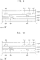
- FIGS. 9 and 10 are cross-sectional views illustrating embodiments taken along line I-I' of FIG. 4 .
- FIG. 10 may be substantially the same as FIG. 9 except for a location where the data input line DIL is disposed.
- an embodiment of the display device may include a substrate SUB, a first interlayer insulating layer ILD1, a second interlayer insulating layer ILD2, a third interlayer insulating layer ILD3, a first voltage line VL1, a second voltage line VL2, a third voltage line and a data input line DIL.
- the substrate SUB may include a plastic or a glass.
- the display device may have flexible characteristics.
- the display device may have rigid characteristics.
- the second voltage output line VO2 may be disposed on the substrate SUB.
- the initialization voltage VINT may be applied to the second voltage output line VO2.
- the second voltage output line VO2 may be connected to the pixel P disposed in the display area DA.
- the data input line DIL may be disposed on the substrate SUB.
- the data input line DIL and the second voltage output line VO2 may be disposed in (or directly on) a same layer.
- the data input line DIL may be disposed on the first interlayer insulating layer ILD1.
- the data input line DIL and the second voltage output line VO2 may be disposed in or (directly on) different layers from each other.
- two or more data input lines DIL may be disposed on the substrate SUB.
- the two or more data lines DIL may be disposed in a same layer as or different layers from each other.
- one of the two or more data lines DIL may be disposed on the first interlayer insulating layer ILD1
- another of the two or more data lines DIL may be disposed between the first interlayer insulating layer ILD1 and the substrate SUB.
- the first interlayer insulating layer ILD1 may be disposed on the substrate SUB to cover the second voltage output line VO2.
- the first interlayer insulating layer ILD1 may include an insulating material.
- the first interlayer insulating layer ILD1 may include an inorganic insulating material such as silicon oxide, silicon nitride, and silicon oxynitride.
- the first voltage transmission line VC1 may be disposed on the first interlayer insulating layer ILD1.
- the initialization voltage VINT may be applied to the first voltage transmission line VC1.
- the first voltage transmission line VC1 may be connected to the second voltage output line VO2 through a contact hole, such that the initialization voltage VINT applied to the first voltage transmission line VC1 may flow to the second voltage output line VO2.
- the second interlayer insulating layer ILD2 may be disposed on the first interlayer insulating layer ILD1 to cover the first voltage transmission line VC1 and the data input line DIL.
- the second interlayer insulating layer ILD2 may include an insulating material.
- the second interlayer insulating layer ILD2 may include an inorganic insulating material such as silicon oxide, silicon nitride, and silicon oxynitride.
- the first to third voltage lines VL1, VL2, VL3 may be disposed on the second interlayer insulating layer ILD2.
- different types of voltages may be applied to the first to third voltage lines VL1, VL2, VL3, respectively.
- the initialization voltage VINT may be applied to the first voltage line VL1
- the low power voltage VSS may be applied to the second voltage line VL2
- the high power voltage VDD may be applied to the third voltage line VL3.
- the low power voltage VSS may be applied to the first voltage line VL1
- the initialization voltage VINT may be applied to the second voltage line VL2
- the high power voltage VDD may be applied to the third voltage line VL3.
- the third interlayer insulating layer ILD3 may be disposed on the second interlayer insulating layer ILD2 to cover the first to third voltage lines VL1, VL2, VL3.
- the third interlayer insulating layer ILD3 may include an insulating material.
- the third interlayer insulating layer ILD3 may include an inorganic insulating material such as silicon oxide, silicon nitride, and silicon oxynitride.
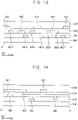
- FIGS. 11, 12 and 13 are cross-sectional views illustrating embodiments taken along line II-II' of FIG. 4 .
- an embodiment of the display device may include a substrate SUB, first to third interlayer insulating layer ILD1, ILD2, ILD3, a third voltage line VL3, a second voltage output line VO2, a third voltage output line VO3, and a plurality of data output lines DOL1, DOL2, DOL3, DOL4, DOL5, DOL6, DOL7.
- the plurality of data output lines DOL1, DOL2, DOL3, DOL4, DOL5, DOL6, DOL7 may be disposed on the substrate SUB.
- the data signal DATA may be applied to the plurality of data output lines DOL1, DOL2, DOL3, DOL4, DOL5, DOL6, DOL7.
- the plurality of data output lines DOL1, DOL2, DOL3, DOL4, DOL5, DOL6, DOL7 may transmit the data signal DATA to the pixels P.
- the first interlayer insulating layer ILD1 may be disposed on the substrate SUB to cover the plurality of data output lines DOL1, DOL2, DOL3, DOL4, DOL5, DOL6, DOL7.
- the first interlayer insulating layer ILD1 may include an insulating material.
- the second voltage output line VO2 and the third voltage output line VO3 may be disposed on the plurality of data output lines DOL1, DOL2, DOL3, DOL4, DOL5, DOL6, DOL7.
- the plurality of data output lines DOL1, DOL2, DOL3, DOL4, DOL5, DOL6, DOL7 may be disposed on the second voltage output line VO2 and the third voltage output line VO3.
- some of the plurality of data output lines DOL2, DOL4, DOL7 and the rest of the plurality of data output lines DOL1, DOL3, DOL5, DOL6 may be disposed in different layers from each other.
- the second voltage output line VO2 and the third voltage output line VO3 may be disposed in different layers from each other.
- the lines may be disposed in different layers from each other to minimize the non-display area NDA.
- the second interlayer insulating layer ILD2 may be disposed on the first interlayer insulating layer ILD1 to cover the second voltage output line VO2 and the third voltage output line VO3.
- the second interlayer insulating layer ILD2 may include an insulating material.
- the third voltage line VL3 may be disposed on the second interlayer insulating layer ILD2.
- the third voltage line VL3 illustrated in FIGS. 11 to 13 may correspond to the output unit VP of FIG. 4 .
- the third interlayer insulating layer ILD3 may be disposed on the second interlayer insulating layer ILD2 to cover the third voltage line VL3.
- the third interlayer insulating layer ILD3 may include an insulating material.
- FIGS. 14 and 15 are cross-sectional views illustrating embodiments taken along line III-III' of FIG. 5 .
- an embodiment of the display device may include a substrate SUB, first to third interlayer insulating layers ILD1, ILD2, ILD3, fourth to sixth voltage output lines VO4, VO5, VO6, a first voltage line VL1, a third voltage line VL3 and a second voltage transmission line VC2.
- the fifth voltage output line VO5 and the sixth voltage output line VO6 may be disposed on the substrate SUB.
- the initialization voltage VINT may be applied to the fifth voltage output line VO5 and the sixth voltage output line VO6.
- the first interlayer insulating layer ILD1 may be disposed on the substrate SUB to cover the fifth voltage output line VO5 and the sixth voltage output line VO6.
- the first interlayer insulating layer ILD1 may include an insulating material.
- the fourth voltage output line VO4 and the second voltage transfer line VC2 may be disposed on the first interlayer insulating layer ILD1.
- the initialization voltage VINT may be applied to the fourth voltage output line VO4 and the second voltage transfer line VC2, respectively.
- the fourth voltage output line VO4 and the second voltage transmission line VC2 may be disposed on the first interlayer insulating layer ILD1.
- the initialization voltage VINT may be applied to the fourth voltage output line VO4 and the second voltage transmission line VC2, respectively.
- the second interlayer insulating layer ILD2 may be disposed on the first interlayer insulating layer ILD1 to cover the fourth voltage output line VO4 and the second voltage transmission line VC2.
- the second interlayer insulating layer ILD2 may include an insulating material.
- the first voltage line VL1 and the third voltage line VL3 may be disposed on the second interlayer insulating layer ILD2.
- the initialization voltage VINT may be applied to the first voltage line VL1.
- the first voltage line VL1 may be connected to the fourth voltage output line VO4 and the second voltage transmission line VC2, respectively, through a contact hole.
- the first voltage line VL1 may connect a fourth voltage output line VO4 and the second voltage transmission line VC2 to each other.
- the initialization voltage VINT applied to the first voltage line VL1 may be transferred to the fourth to sixth output lines VO4, VO5, VO6, respectively.
- the high power voltage ELVDD may be applied to the third voltage line VL3.
- the third interlayer insulating layer ILD3 may be disposed on the second interlayer insulating layer ILD2 to cover the first voltage line VL1 and the third voltage line VL3.
- the third interlayer insulating layer ILD3 may include an insulating material.
- the fourth voltage output line VO4 may be disposed in a same layer as the fifth and sixth voltage output lines VO5, VO6.
- lines may be disposed in various layers to minimize an area of the display device.
- the lines are disposed directly on the substrate, but not being limited thereto.
- an additional insulating layer e.g., a buffer layer, a barrier layer, a gate insulating layer, an interlayer insulating layer, etc.
- the lines may be disposed on the additional insulating layer.
- an insulating layer and/or conductive layers may be further disposed on the substrate SUB, and the lines may be disposed on the insulating layer and/or the conductive layers.
- Embodiments described herein may be applied to various display devices, for example, vehicle-display device, a ship-display device, an aircraft-display device, portable communication devices, display devices for display or for information transfer, a medical-display device, etc.
Landscapes
- Engineering & Computer Science (AREA)
- Physics & Mathematics (AREA)
- General Physics & Mathematics (AREA)
- Theoretical Computer Science (AREA)
- Computer Hardware Design (AREA)
- Microelectronics & Electronic Packaging (AREA)
- Devices For Indicating Variable Information By Combining Individual Elements (AREA)
- Electroluminescent Light Sources (AREA)
Abstract
Description
- Embodiments relate to a display device, and particularly, a display device including a plurality of lines.
- Recently, interest in display devices is increasing. Accordingly, the display device is manufactured in various types, including an organic light emitting display device, a liquid crystal display device, and a quantum-dot nano light emitting display device.
- In addition, a form of the display device has been diversified. For example, the display device may have a shape such as a circle or a polygon. Alternatively, the display device may have a shape in which each vertex of a polygon has a curvature.
- A plurality of lines may be disposed in a non-display area of the display device. For example, a low power voltage line, an initialization voltage line, a high power voltage line, and a data line may be disposed in a non-display area of a circular display device. In such a circular display device, a dead space may be formed by a space in which the low power voltage line, the initialization voltage line, the high power voltage line, and the data line are disposed.
- Embodiments provide a display device with reduced dead space.
- According to an embodiment, a display device includes a substrate on which a display area including a plurality of pixels and a non-display area surrounding the display area are defined, a first voltage line disposed on the substrate in the non-display area, where the first voltage line provides a first voltage to the pixels, a second voltage line disposed on the substrate in the non-display area, where the second voltage line provides a second voltage to the pixels, and a first demux circuit area and a second demux circuit area disposed on the substrate in the non-display area, where the first demux circuit area and the second demux circuit area transmit data signals to the pixels. In such an embodiment, the first voltage line passes an area between the first demux circuit area and the second demux circuit area.
- In an embodiment, the display area may have a circular shape or another round shape, such as an elliptical shape, especially a curved or round shape without straight edges and vertexes.
- In an embodiment, the display device may further include a first voltage bypass line connected to the first voltage line and disposed along an edge of the display area and a second voltage bypass line connected to the second voltage line and disposed along the edge of the display area.
- In an embodiment, the first voltage may be an initialization voltage, and the second voltage may be a low power voltage.
- In an embodiment, the first voltage may be a low power voltage, and the second voltage may be an initialization voltage.
- In an embodiment, the first demux circuit area and the second demux circuit area may be disposed to be spaced apart in one direction. The one direction may be the longitudinal direction of a circuit board disposed on one side of the non-display area.
- In an embodiment, the display device may further include a third voltage line disposed on the substrate in the non-display area, where the third voltage line may provide a third voltage to the pixels.
- In an embodiment, the third voltage may be a high power voltage.
- In an embodiment, a part of the third voltage line may pass the area between the first demux circuit area and the second demux circuit area.
- In an embodiment, a width of the part of the third voltage line may be narrower than a width of another part of the third voltage line connected to the part.
- In an embodiment, the display device may further include a plurality of voltage output lines connected to the first voltage line.
- In an embodiment, some of the voltage output lines may partially overlap the first demux circuit area, and others of the voltage output lines except for the some partially may overlap the second demux circuit area.
- In an embodiment, the display device may further include a voltage transmission line connected to the first voltage line. In such an embodiment, at least some of the voltage output lines may be connected to the first voltage line by the voltage transmission line.
- In an embodiment, some of the voltage transmission lines may overlap the first demux circuit area, and others of the voltage transmission lines except for the some may overlap the second demux circuit area.
- In an embodiment, the first voltage line and the voltage output line may be disposed in different layers from each other.
- In an embodiment, the plurality of voltage output lines may be disposed in a same layer.
- In an embodiment, at least some of the plurality of voltage output lines may be disposed in different layers from each other.
- In an embodiment, the first demux circuit area may include a first demux circuit to which a first data signal is applied through a first data input line, and the second demux circuit area may include a second demux circuit to which a second data signal is applied through a second data input line.
- In an embodiment, the first data input line and the second data input line may be disposed in a same layer.
- In an embodiment, the first data input line and the second data input line may be disposed in different layers from each other.
- In an embodiment, the display device may further include a first data output line and a second data output line, which are connected to the first demux circuit and a third data output line and a fourth data output line, which are connected to the second demux circuit.
- In an embodiment, the first to fourth data output lines may be disposed in a same layer.
- In an embodiment, at least one selected from the first to fourth data output lines may be disposed in a different layer from another selected therefrom.
- In an embodiment, the first voltage line may include a first part disposed between the first demux circuit and the second demux circuit, and a second part connected to the first part, and a width of the first part may be narrower than a width of the second part.
- According to embodiments, the display device may include a substrate on which a display area including a plurality of pixels and a non-display area surrounding the display area are defined, a first voltage line disposed on the substrate in the non-display area to provide a first voltage to the pixels, a second voltage line disposed on the substrate in the non-display area to provide a second voltage to the pixels, and a first demux circuit area and a second demux circuit area disposed on the substrate in the non-display area to transmit data signals to the pixels. In such embodiments, the first voltage line may pass an area between the first demux circuit area and the second demux circuit area.
- Accordingly, in such embodiments of the display device, the non-display area at the lower end of the display device may be reduced compared to a case where the first voltage line is disposed to bypass a demux circuit area.
- Features of embodiments of the invention will be more clearly understood from the following detailed description taken in conjunction with the accompanying drawings.
-
FIG. 1 is a plan view illustrating a display device according to an embodiment. -
FIG. 2 is a circuit diagram illustrating a pixel included in the display device ofFIG. 1 . -
FIG. 3 is a diagram illustrating an embodiment in which area A of the display device ofFIG. 1 is enlarged. -
FIG. 4 is a diagram illustrating an embodiment in which area B of the display device ofFIG. 1 is enlarged. -
FIG. 5 is a diagram illustrating an embodiment in which area B of the display device ofFIG. 1 is enlarged. -
FIG. 6 is a diagram illustrating an embodiment in which area A of the display device ofFIG. 1 is enlarged. -
FIG. 7 is a diagram illustrating an embodiment in which area B of the display device ofFIG. 1 is enlarged. -
FIG. 8A is a diagram illustrating an embodiment in which area B of the display device ofFIG. 1 is enlarged. -
FIG. 8B is a diagram schematically illustrating a structure of a demux circuit illustrated inFIG. 8A . -
FIGS. 9 and 10 are cross-sectional views illustrating embodiments taken along line I-I' ofFIG. 4 . -
FIGS. 11, 12 and13 are cross-sectional views illustrating embodiments taken along line II-II' ofFIG. 4 . -
FIGS. 14 and15 are cross-sectional views illustrating embodiments taken along line III-III' ofFIG. 5 . - The invention now will be described more fully hereinafter with reference to the accompanying drawings, in which various embodiments are shown. This invention may, however, be embodied in many different forms, and should not be construed as limited to the embodiments set forth herein. Rather, these embodiments are provided so that this disclosure will be thorough and complete, and will fully convey the scope of the invention to those skilled in the art. Like reference numerals refer to like elements throughout.
- It will be understood that when an element is referred to as being "on" another element, it can be directly on the other element or intervening elements may be present therebetween. In contrast, when an element is referred to as being "directly on" another element, there are no intervening elements present.
- It will be understood that, although the terms "first," "second," "third" etc. may be used herein to describe various elements, components, regions, layers and/or sections, these elements, components, regions, layers and/or sections should not be limited by these terms. These terms are only used to distinguish one element, component, region, layer or section from another element, component, region, layer or section. Thus, "a first element," "component," "region," "layer" or "section" discussed below could be termed a second element, component, region, layer or section without departing from the teachings herein.
- The terminology used herein is for the purpose of describing particular embodiments only and is not intended to be limiting. As used herein, "a", "an," "the," and "at least one" do not denote a limitation of quantity, and are intended to include both the singular and plural, unless the context clearly indicates otherwise. For example, "an element" has the same meaning as "at least one element," unless the context clearly indicates otherwise. "At least one" is not to be construed as limiting "a" or "an." "Or" means "and/or." As used herein, the term "and/or" includes any and all combinations of one or more of the associated listed items. It will be further understood that the terms "comprises" and/or "comprising," or "includes" and/or "including" when used in this specification, specify the presence of stated features, regions, integers, steps, operations, elements, and/or components, but do not preclude the presence or addition of one or more other features, regions, integers, steps, operations, elements, components, and/or groups thereof.
- Furthermore, relative terms, such as "lower" or "bottom" and "upper" or "top," may be used herein to describe one element's relationship to another element as illustrated in the Figures. It will be understood that relative terms are intended to encompass different orientations of the device in addition to the orientation depicted in the Figures. For example, if the device in one of the figures is turned over, elements described as being on the "lower" side of other elements would then be oriented on "upper" sides of the other elements. The term "lower," can therefore, encompasses both an orientation of "lower" and "upper," depending on the particular orientation of the figure. Similarly, if the device in one of the figures is turned over, elements described as "below" or "beneath" other elements would then be oriented "above" the other elements. The terms "below" or "beneath" can, therefore, encompass both an orientation of above and below.
- Unless otherwise defined, all terms (including technical and scientific terms) used herein have the same meaning as commonly understood by one of ordinary skill in the art to which this disclosure belongs. It will be further understood that terms, such as those defined in commonly used dictionaries, should be interpreted as having a meaning that is consistent with their meaning in the context of the relevant art and the present disclosure, and will not be interpreted in an idealized or overly formal sense unless expressly so defined herein.
- Embodiments are described herein with reference to cross section illustrations that are schematic illustrations of idealized embodiments. As such, variations from the shapes of the illustrations as a result, for example, of manufacturing techniques and/or tolerances, are to be expected. Thus, embodiments described herein should not be construed as limited to the particular shapes of regions as illustrated herein but are to include deviations in shapes that result, for example, from manufacturing. For example, a region illustrated or described as flat may, typically, have rough and/or nonlinear features. Moreover, sharp angles that are illustrated may be rounded. Thus, the regions illustrated in the figures are schematic in nature and their shapes are not intended to illustrate the precise shape of a region and are not intended to limit the scope of the present claims.
- Hereinafter, embodiments of the disclosure will be described in detail with reference to the accompanying drawings.
-
FIG. 1 is a plan view illustrating a display device according to an embodiment, andFIG. 2 is a circuit diagram illustrating a pixel included in the display device ofFIG. 1 . - Referring to
FIGS. 1 and2 , an embodiment of the display device may include a display area DA and a non-display area NDA surrounding the display area DA. In an embodiment, the display area DA may have a curvature. In an embodiment, for example, the display area DA may have a circular shape having a constant curvature as a whole. Alternatively, the display area DA may include a part having a linear shape or a straight outer side, and another part having a shape having a curvature or a curved outer side. - A plurality of pixels P may be disposed in the display area DA. The pixels P may be arranged in various shapes in the display area DA. In an embodiment, for example, the pixels P may be entirely arranged in a matrix form in the display area DA. Alternatively, the pixels P may be arranged in a matrix form in a central part of the display area DA, and may be arranged in a stepwise manner at a edge of the display area DA. In such embodiments, the pixels P may be arranged in various shapes corresponding to a shape of the display area DA for displaying an image thereon.
- Each of the pixels P may include at least one transistor and at least one capacitor.
FIG. 2 illustrates an embodiment of a pixel including seven transistors and a single capacitor. In an embodiment, each of the pixels P may include first to seventh transistors TR1, TR2, TR3, TR4, TR5, TR6, TR7, and a storage capacitor CST, as shown inFIG. 2 . In an embodiment, the display device may be an organic light emitting display device, and each of the pixels P may further include an organic light emitting diode OLED. Alternatively, each of the pixels P may include three transistors and a single capacitor. In such embodiments, each of the pixels P may include various numbers of transistors and capacitors for driving the pixels P. - In an embodiment, as shown in
FIG. 2 , each of the pixels P may receive a data signal DATA, gate signals GW, GI, GB, an light emitting signal EM, a high power voltage ELVDD, a low power voltage ELVSS, and an initialization voltage VINT, but not being limited thereto. Alternatively, an additional voltage (e.g., a compensation voltage) may be further applied to each of the pixels P. - The non-display area NDA may have a shape corresponding to the shape of the display area DA. In an embodiment, for example, the display area DA may have a circular shape, and the non-display area NDA may have a circular shape (or a circular band shape) having a same curvature as the display area DA. Alternatively, the non-display area NDA may have a shape independent from the display area DA. In an embodiment, for example, the display area DA may have a circular shape, and the non-display area NDA may have a polygonal shape.
- In an embodiment, a plurality of demux circuits may be disposed on one side portion of the non-display area NDA. Each of the demux circuits may output the data signal DATA through a plurality of data output lines after receiving the data signal DATA from a data input line. In such an embodiment, the display device may efficiently utilize a space in which the lines are arranged in the non-display area NDA. The demux circuits may be disposed in a demux circuit area DXA. The demux circuit area DXA may be disposed adjacent to the display area DA. In an embodiment, the demux circuit area DXA and the display area DA may be disposed adjacent to each other in a first direction DR1. The demux circuit area DXA may extend in a second direction DR2 perpendicular to the first direction DR1. In such an embodiment, the demux circuits may be arranged in parallel in the second direction DR2. Alternatively, the demux circuit area DXA may extend to correspond to the curvature of the display area DA. In such an embodiment, the demux circuits may be disposed along the edge of the display area DA.
- In an embodiment, a circuit board CB may be disposed on one side of the non-display area NDA. The circuit board CB may transmit various signals and voltages to the pixels P. The circuit board CB may be disposed on or to overlap the non-display area NDA, or may be disposed to be connected to the non-display area NDA by a separate film. Lines extending from the circuit board CB may be connected to the display area DA after passing through the non-display area NDA.
FIG. 1 shows only a portion of the lines for convenience of illustration, and the display device may include more lines. The lines may be entirely disposed along the edge of the display area DA, or may be disposed only in a part of the edge. -
FIG. 3 is a diagram illustrating an embodiment in which area A of the display device ofFIG. 1 is enlarged. - Referring to
FIGS. 1 and3 , an embodiment of the display device may include a plurality of lines. In an embodiment, some of the lines may be disposed along the edge of the display area DA. In an embodiment, for example, a first voltage bypass line VBL1 and a second voltage bypass line VBL2 may be disposed along the edge of the display area DA. In such an embodiment, each of the first voltage bypass line VBL1 and the second voltage bypass line VBL2 may have a curvature. Each of the first voltage bypass line VBL1 and the second voltage bypass line VBL2 may be connected to voltage lines to be described later. The first voltage bypass line VBL1 may be connected to the pixels P by a plurality of lines. The second voltage bypass line VBL2 may be connected to the pixels P by a plurality of lines. -
FIG. 4 is a diagram illustrating an embodiment in which area B of the display device ofFIG. 1 is enlarged. - Referring to
FIGS. 1 ,2 ,3 and4 , an embodiment of the display device may include a first voltage line VL1, a second voltage line VL2, a third voltage line VL3, a first voltage transmission line VC1, first to sixth voltage output lines VO1, VO2, VO3, VO4, VO5, VO6. In an embodiment, the display device may include a first demux circuit area DXA1 and a second demux circuit area DXA2. In an embodiment, a demux circuit (e.g., one or more demux circuits) may be disposed in each of the first demux circuit area DXA1 and a second demux circuit area DXA2. - In an embodiment, a first voltage may be applied to the first voltage line VL1. In an embodiment, the initialization voltage VINT may be applied to the first voltage line VL1 as the first voltage. In such an embodiment, the first voltage line VL1 may pass (or extend through) an area between the first demux circuit area DXA1 and the second demux circuit area DXA2. The first demux circuit area DXA1 and the second demux circuit area DXA2 may be spaced apart from each other by the first voltage line VL1. When used herein, the term spaced apart from each other by a signal or voltage line means that the respective mentioned areas, especially circuit areas, are spaced apart from each other by a distance and the respective mentioned line is located in or protrudes through this distance. In such an embodiment, unlike the second voltage line VL2, the first voltage line VL1 does not bypass the first demux circuit area DXA1, thereby reducing the non-display area NDA of the display device.
- In an embodiment, the first voltage line VL1 may be connected to the first voltage transmission line VC1 through a contact hole. The first voltage transmission line VC1 may be connected to the first to sixth voltage output lines V01, VO2, VO3, VO4, VO5, VO6 through a contact hole, respectively. The initialization voltage VINT flowing through the first voltage line VL1 may be transferred to the pixels P through the first voltage transmission line VC1 and the first to sixth voltage output lines V01, VO2, VO3, VO4, VO5, VO6.
- The first voltage transmission line VC1 may be partially disposed to overlap the first demux circuit area DXA1 and the second demux circuit area DXA2. The first to sixth voltage output lines V01, VO2, VO3, VO4, VO5, VO6 may be partially disposed to overlap the first demux circuit area DXA1 and the second demux circuit area DXA2. In an embodiment, the first to sixth voltage output lines V01, VO2, VO3, VO4, VO5, VO6 may pass an area between the demux circuits. The demux circuits and the first to sixth voltage output lines V01, VO2, VO3, VO4, VO5, VO6 may be disposed not to overlap each other.
- In an embodiment, the first voltage transmission line VC1 and the first to sixth voltage output lines V01, VO2, VO3, VO4, VO5, VO6 may be disposed on different layers. In an embodiment, as illustrated in
FIG. 4 , the first voltage transmission line VC1 may be disposed above the first to sixth voltage output lines V01, VO2, VO3, VO4, VO5, VO6. Alternatively, the first voltage transfer line VC1 may be disposed below the first to sixth voltage output lines V01, VO2, VO3, VO4, VO5, and VO6. - In an embodiment, the first voltage transmission line VC1 may be connected to the first voltage bypass line VBL1. In an embodiment, for example, the first voltage transmission line VC1 may be integrally formed with the first voltage bypass line VBL1 as a single unitary unit. Alternatively, the first voltage transmission line VC1 may be connected to the first voltage bypass line VBL1 through a contact hole.
- In an embodiment, the initialization voltage VINT may flow along the edge of the display area DA through the first voltage bypass line VBL1. In such an embodiment, the first voltage bypass line VBL1 may apply the initialization voltage VINT to the pixels P by lines connecting the first voltage bypass line VBL1 and the pixels P.
- The first voltage line VL1 may include a first part VLA1 disposed between the first demux circuit area DXA1 and the second demux circuit area DXA2, and a second part VLA2 connected to the first part VLA2. In an embodiment, a width of the first part VLA1 may be narrower than a width of the second part VLA2. In such an embodiment where the width of the first portion VLA1 is narrower than the width of the second part VLA2, an area between the first demux circuit area DXA1 and the second demux circuit area DXA2 that are spaced apart from each other may be minimized.
- A second voltage different from the first voltage may be applied to the second voltage line VL2. In an embodiment, the low power voltage ELVSS may be applied to the second voltage line VL2 as the second voltage. The second voltage line VL2 may be connected to the second voltage bypass line VBL2. In an embodiment, the low power voltage ELVSS may flow along the edge of the display area DA through the second voltage bypass line VBL2. In such an embodiment, the second voltage bypass line VBL2 may apply the low power voltage ELVSS to the pixels P by lines connecting the second voltage bypass line VBL2 and the pixels P.
- In an embodiment, the low power voltage ELVSS may be applied to the first voltage line VL1, and the initialization voltage VINT may be applied to the second voltage line VL2.
- As described above, in an embodiment of the display device, the first voltage bypass line VBL1 may be connected to the first voltage line VL1 passing between the first demux circuit area DXA1 and the second demux circuit area DXA2, thereby reducing the non-display area NDA at the lower part of the display device. In such an embodiment of the display device, the non-display area NDA at the lower part of the display device may be reduced compared to a case where the first voltage line VL1 is turned to the outside of the demux circuit area DXA and is connected to the first voltage bypass line VBL1.
- A third voltage different from the first voltage and the second voltage may be applied to the third voltage line VL3. In embodiments, the high power voltage ELVDD may be applied to the third voltage line VL3 as the third voltage. The high power voltage ELVDD may be applied to the third voltage line VL3 by a plurality of input units. The third voltage line VL3 may be disposed to surround the second demux circuit area DXA2. Thus, the third voltage line VL3 may comprise several sections or parts which may be disposed to surround the second demux circuit area DXA2. On a plan view, a plurality of demux circuits may be disposed between the third voltage line VL3 or between the different sections or parts of the third voltage line VL3. The first demux circuit area DXA1 and the second demux circuit area DXA2 may be spaced apart from each other by the third voltage line VL3 or by a section or part of the third voltage line VL3. The third voltage line VL3 may provide the high power voltage ELVDD to the pixels P by a plurality of output units VP.
- In an embodiment, the first demux circuit area DXA1 and the second demux circuit area DXA2 may be spaced apart by the third voltage line VL3 or by a section or part of the third voltage line VL3. In an embodiment, a width of a first part of the third voltage line VL3 disposed between the first demux circuit area DXA1 and the second demux circuit area DXA2 may be narrower than a width of other part of the third voltage line VL3 connected to the first part, such that a space between the first demux circuit area DXA1 and the second demux circuit area DXA2, which are spaced apart from each other, may be minimized. The other part of the third voltage line VL3, which may be termed as a second part, may extend angular (with an angel other than 0° and 180°) or perpendicular to the first part. The third voltage line VL3 may comprise further parts parallel or angular (with an angel other than 0° and 180°) or perpendicular to the first part and/or second part.
-
FIG. 5 is a diagram illustrating an embodiment in which area B of the display device ofFIG. 1 is enlarged.FIG. 5 may be substantially the same asFIG. 4 except for lines to which the initialization voltage VINT is applied. The same or like elements shown inFIG. 5 have been labeled with the same reference characters as used above to describe the embodiment of the display device shown inFIG. 1 , and any repetitive detailed description thereof will hereinafter be omitted or simplified. - Referring to
FIGS. 1 ,2 ,3 and5 , in an embodiment, the first voltage line VL1 may be directly connected to the first to fourth voltage output lines V01, VO2, VO3, VO4 through a contact hole. In such an embodiment, the first voltage line VL1 may be connected to the second voltage transmission line VC2 through a contact hole, and the fifth and sixth voltage output lines VO5, VO6 may be connected to the second voltage transmission line VC2 through a contact hole. In such an embodiment, the fifth and sixth voltage output lines VO5, VO6 may be connected to the first voltage line VL1 by the second voltage transmission line VC2. The second voltage transmission line VC2 may be disposed to be spaced apart from the second demux circuit area DXA2. In such an embodiment, the second voltage transmission line VC2 may not overlap the second demux circuit area DXA2. In such an embodiment, the first to sixth voltage output lines V01, VO2, VO3, VO4, VO5, VO6 may partially overlap the second demux circuit area DXA2. - In an embodiment, the first voltage line VL1 may be connected to the first bypass line VBL1. In an embodiment, for example, the first voltage line VL1 may be integrally formed with the first voltage bypass line VBL1 as a single unitary unit. Alternatively, the first voltage line VL1 may be connected to the first voltage bypass line VBL1 through a contact hole.
- In such an embodiment, the first voltage line VL1 passes an area between the first demux circuit area DXA1 and the second demux circuit area DXA2 and is connected to the first voltage bypass line VBL1, such that the area of the lower end of the non-display area NDA of the display device may be reduced.
-
FIG. 6 is a diagram illustrating an embodiment in which area A of the display device ofFIG. 1 is enlarged. - Referring to
FIGS. 1 and6 , an embodiment of the display device may include a plurality of lines. the plurality of lines may be disposed along an edge of the display area DA. In an embodiment, for example, a first voltage bypass line VBL1, a second voltage bypass line VBL2 and a third voltage bypass line VBL3 may be disposed along the edge of the display area DA. In such an embodiment, each of the first voltage bypass line VBL1, the second voltage bypass line VBL2, and the third voltage bypass line VBL3 may have a curvature. Each of the first voltage bypass line VBL1, the second voltage bypass line VBL2, and the third voltage bypass line VBL3 may be connected to voltage lines to be described later. Each of the first voltage bypass line VBL1, the second voltage bypass line VBL2, and the third voltage bypass line VBL3 may be connected to the pixels P by separate lines. -
FIG. 7 is a diagram illustrating an embodiment in which area B of the display device ofFIG. 1 is enlarged. - Referring to
FIGS. 1 ,2 ,6 and7 , an embodiment of the display device may include a first voltage line VL1, a second voltage line VL2, a third voltage line VL3, a fourth voltage line VL4, a first voltage transmission line VC1, a third voltage transmission line VC3, first to sixth voltage output lines VO1, VO2, VO3, VO4, VO5, VO6 and seventh to twelfth voltage output lines VO7, VO8, VO9, VO10, VO11, V012. In an embodiment, the display device may include a first demux circuit area DXA1 and a second demux circuit area DXA2. In an embodiment, a demux circuit may be disposed in each of the first demux circuit area DXA1 and the second demux circuit area DXA2. - The fourth voltage line VL4 may be disposed between the first voltage line VL1 and the second voltage line VL2. An additional voltage may be applied to the fourth voltage line VL4 as desired. The fourth voltage line VL4 may be connected to the third voltage transmission line VC3. The third voltage transmission line VC may be connected to the seventh to twelfth voltage output lines VO7, VO8, VO9, VO10, VO11, VO12 through a contact hole. The seventh to twelfth voltage output lines VO7, VO8, VO9, VO10, VO11, VO12 are connected to the pixels P, respectively, to provide the additional voltage to the pixels P. The voltage applied to the fourth voltage line VL4 is applied to the pixels P through the third transmission line VC3 and the seventh to twelfth voltage output lines VO7, VO8, VO9, VO10, VO11, VO12. In an embodiment, the third voltage transmission line VC3 may partially overlap the first demux circuit area DXA1 and the second demux circuit area DXA2. In such an embodiment, the first to twelfth voltage output lines VO1, VO2, VO3, VO4, VO5, VO6, VO7, VO8, VO9, VO10, VO11, VO12 may also partially overlap the first demux circuit area DXA1 and the second demux circuit area DXA2. In such an embodiment, the first to twelfth voltage output lines VO1, VO2, VO3, VO4, VO5, VO6, VO7, VO8, VO9, VO10, VO11, VO12 may not overlap the demux circuits.
- In an embodiment, the fourth voltage line VL4 and the seventh to twelfth voltage output lines VO7, VO8, VO9, VO10, VO11, VO12 may be disposed in different layers from each other.
- In an embodiment, the fourth voltage line VL4 may include a first part VLA3 disposed between the first demux circuit area DXA1 and the second demux circuit area DXA2 and a second part VLA4 connected to the first part VLA3. In such an embodiment, the first part VLA3 may have a narrower width than the second part VLA4, such that an area between the first demux circuit area DXA1 and the second demux circuit area DXA2, which are spaced apart from each other, may be minimized.
-
FIG. 8A is a diagram illustrating an embodiment in which area B of the display device ofFIG. 1 is enlarged, andFIG. 8B is a diagram schematically illustrating a structure of a demux circuit illustrated inFIG. 8A . - Referring to
FIGS. 1 ,2 and8A , in an embodiment, at least one demux circuit DC may be disposed in each of the first demux circuit area DXA1 and the second demux circuit area DXA2. Each of the demux circuits DC may be connected to data input lines DIL. The data signal DATA transmitted from the circuit film CF may be transmitted to the demux circuits DC through the data input lines DIL. Each of the demux circuits DC may transmit the data signal DATA to the pixels P through data output lines DOL. In an embodiment, as shown inFIG. 8A , two data output lines DOL are connected to one demux circuit DC, for example, but not being limited thereto. In one alternative embodiment, for example, the demux circuits DC may also be connected to three or more data output lines DOL. Alternatively, some of the demux circuits DC may be connected to n data output lines DOL, and the rest of the demux circuits DC may be connected to m data output lines DOL (however, n and m is a natural number of 2 or greater). The data input lines DIL and the data output lines DOL connected to the pixels P may be efficiently connected through the demux circuit DC. Each of the voltage output lines described above with reference toFIGS. 4 to 7 may be disposed between the demux circuits DC. In such an embodiment, the voltage output lines may not overlap the demux circuits DC. - Referring to
FIGS. 8A and8B , each of the demux circuits DC may include at least two transistors T1, T2. The demux circuits DC may be connected to a first signal line G1 and a second signal line G2, respectively. A signal may selectively flow through the first signal line G1 and the second signal line G2. When the first signal line G1 transmits a signal to the first transistor T1, the first transistor T1 may be turned on. When the first transistor T1 is turned on, the data signal DATA ofFIG. 2 may be output to the data output line DOL through the first transistor T1. In such an embodiment, when the second signal line G2 transmits a signal to the second transistor T2, the second transistor T2 may be turned on. When the second transistor T2 is turned on, the data signal DATA ofFIG. 2 may be output to the data output line DOL through the second transistor T2. -
FIGS. 9 and 10 are cross-sectional views illustrating embodiments taken along line I-I' ofFIG. 4 .FIG. 10 may be substantially the same asFIG. 9 except for a location where the data input line DIL is disposed. - Referring to
FIGS. 1 ,2 4 ,8A and9 , an embodiment of the display device may include a substrate SUB, a first interlayer insulating layer ILD1, a second interlayer insulating layer ILD2, a third interlayer insulating layer ILD3, a first voltage line VL1, a second voltage line VL2, a third voltage line and a data input line DIL. - The substrate SUB may include a plastic or a glass. In an embodiment where the substrate SUB includes the plastic, the display device may have flexible characteristics. In an embodiment where the substrate SUB includes the glass, the display device may have rigid characteristics.
- The second voltage output line VO2 may be disposed on the substrate SUB. The initialization voltage VINT may be applied to the second voltage output line VO2. The second voltage output line VO2 may be connected to the pixel P disposed in the display area DA.
- In an embodiment, as illustrated in
FIG. 10 , the data input line DIL may be disposed on the substrate SUB. In such an embodiment, the data input line DIL and the second voltage output line VO2 may be disposed in (or directly on) a same layer. - Alternatively, as illustrated in
FIG. 9 , the data input line DIL may be disposed on the first interlayer insulating layer ILD1. In such an embodiment, the data input line DIL and the second voltage output line VO2 may be disposed in or (directly on) different layers from each other. - Alternatively, two or more data input lines DIL may be disposed on the substrate SUB. The two or more data lines DIL may be disposed in a same layer as or different layers from each other. In an embodiment, for example, one of the two or more data lines DIL may be disposed on the first interlayer insulating layer ILD1, and another of the two or more data lines DIL may be disposed between the first interlayer insulating layer ILD1 and the substrate SUB.
- The first interlayer insulating layer ILD1 may be disposed on the substrate SUB to cover the second voltage output line VO2. The first interlayer insulating layer ILD1 may include an insulating material. In an embodiment, for example, the first interlayer insulating layer ILD1 may include an inorganic insulating material such as silicon oxide, silicon nitride, and silicon oxynitride.
- The first voltage transmission line VC1 may be disposed on the first interlayer insulating layer ILD1. The initialization voltage VINT may be applied to the first voltage transmission line VC1. The first voltage transmission line VC1 may be connected to the second voltage output line VO2 through a contact hole, such that the initialization voltage VINT applied to the first voltage transmission line VC1 may flow to the second voltage output line VO2.
- The second interlayer insulating layer ILD2 may be disposed on the first interlayer insulating layer ILD1 to cover the first voltage transmission line VC1 and the data input line DIL. The second interlayer insulating layer ILD2 may include an insulating material. In an embodiment, for example, the second interlayer insulating layer ILD2 may include an inorganic insulating material such as silicon oxide, silicon nitride, and silicon oxynitride.
- The first to third voltage lines VL1, VL2, VL3 may be disposed on the second interlayer insulating layer ILD2. In an embodiment, different types of voltages may be applied to the first to third voltage lines VL1, VL2, VL3, respectively. In an embodiment, for example, the initialization voltage VINT may be applied to the first voltage line VL1, the low power voltage VSS may be applied to the second voltage line VL2, and the high power voltage VDD may be applied to the third voltage line VL3. In an alternative embodiment, the low power voltage VSS may be applied to the first voltage line VL1, the initialization voltage VINT may be applied to the second voltage line VL2, and the high power voltage VDD may be applied to the third voltage line VL3.
- The third interlayer insulating layer ILD3 may be disposed on the second interlayer insulating layer ILD2 to cover the first to third voltage lines VL1, VL2, VL3. The third interlayer insulating layer ILD3 may include an insulating material. In an embodiment, for example, the third interlayer insulating layer ILD3 may include an inorganic insulating material such as silicon oxide, silicon nitride, and silicon oxynitride.
-
FIGS. 11, 12 and13 are cross-sectional views illustrating embodiments taken along line II-II' ofFIG. 4 . - Referring to
FIGS. 1 ,2 ,4 ,8A and11 , an embodiment of the display device may include a substrate SUB, first to third interlayer insulating layer ILD1, ILD2, ILD3, a third voltage line VL3, a second voltage output line VO2, a third voltage output line VO3, and a plurality of data output lines DOL1, DOL2, DOL3, DOL4, DOL5, DOL6, DOL7. - The plurality of data output lines DOL1, DOL2, DOL3, DOL4, DOL5, DOL6, DOL7 may be disposed on the substrate SUB. The data signal DATA may be applied to the plurality of data output lines DOL1, DOL2, DOL3, DOL4, DOL5, DOL6, DOL7. The plurality of data output lines DOL1, DOL2, DOL3, DOL4, DOL5, DOL6, DOL7 may transmit the data signal DATA to the pixels P.
- The first interlayer insulating layer ILD1 may be disposed on the substrate SUB to cover the plurality of data output lines DOL1, DOL2, DOL3, DOL4, DOL5, DOL6, DOL7. The first interlayer insulating layer ILD1 may include an insulating material.
- In an embodiment, as illustrated in
FIG. 11 , the second voltage output line VO2 and the third voltage output line VO3 may be disposed on the plurality of data output lines DOL1, DOL2, DOL3, DOL4, DOL5, DOL6, DOL7. - Alternatively, as illustrated in
FIG. 12 , the plurality of data output lines DOL1, DOL2, DOL3, DOL4, DOL5, DOL6, DOL7 may be disposed on the second voltage output line VO2 and the third voltage output line VO3. - Alternatively, as illustrated in
FIG. 13 , some of the plurality of data output lines DOL2, DOL4, DOL7 and the rest of the plurality of data output lines DOL1, DOL3, DOL5, DOL6 may be disposed in different layers from each other. In such an embodiment, the second voltage output line VO2 and the third voltage output line VO3 may be disposed in different layers from each other. - In such an embodiment, the lines may be disposed in different layers from each other to minimize the non-display area NDA.
- The second interlayer insulating layer ILD2 may be disposed on the first interlayer insulating layer ILD1 to cover the second voltage output line VO2 and the third voltage output line VO3. The second interlayer insulating layer ILD2 may include an insulating material.
- The third voltage line VL3 may be disposed on the second interlayer insulating layer ILD2. The third voltage line VL3 illustrated in
FIGS. 11 to 13 may correspond to the output unit VP ofFIG. 4 . - The third interlayer insulating layer ILD3 may be disposed on the second interlayer insulating layer ILD2 to cover the third voltage line VL3. The third interlayer insulating layer ILD3 may include an insulating material.
-
FIGS. 14 and15 are cross-sectional views illustrating embodiments taken along line III-III' ofFIG. 5 . - Referring to
FIGS. 1 ,2 ,5 , and15 , an embodiment of the display device may include a substrate SUB, first to third interlayer insulating layers ILD1, ILD2, ILD3, fourth to sixth voltage output lines VO4, VO5, VO6, a first voltage line VL1, a third voltage line VL3 and a second voltage transmission line VC2. - The fifth voltage output line VO5 and the sixth voltage output line VO6 may be disposed on the substrate SUB. The initialization voltage VINT may be applied to the fifth voltage output line VO5 and the sixth voltage output line VO6.
- The first interlayer insulating layer ILD1 may be disposed on the substrate SUB to cover the fifth voltage output line VO5 and the sixth voltage output line VO6. The first interlayer insulating layer ILD1 may include an insulating material.
- The fourth voltage output line VO4 and the second voltage transfer line VC2 may be disposed on the first interlayer insulating layer ILD1. The initialization voltage VINT may be applied to the fourth voltage output line VO4 and the second voltage transfer line VC2, respectively.
- The fourth voltage output line VO4 and the second voltage transmission line VC2 may be disposed on the first interlayer insulating layer ILD1. The initialization voltage VINT may be applied to the fourth voltage output line VO4 and the second voltage transmission line VC2, respectively.
- The second interlayer insulating layer ILD2 may be disposed on the first interlayer insulating layer ILD1 to cover the fourth voltage output line VO4 and the second voltage transmission line VC2. The second interlayer insulating layer ILD2 may include an insulating material.
- The first voltage line VL1 and the third voltage line VL3 may be disposed on the second interlayer insulating layer ILD2. The initialization voltage VINT may be applied to the first voltage line VL1. The first voltage line VL1 may be connected to the fourth voltage output line VO4 and the second voltage transmission line VC2, respectively, through a contact hole. The first voltage line VL1 may connect a fourth voltage output line VO4 and the second voltage transmission line VC2 to each other. The initialization voltage VINT applied to the first voltage line VL1 may be transferred to the fourth to sixth output lines VO4, VO5, VO6, respectively. The high power voltage ELVDD may be applied to the third voltage line VL3.
- The third interlayer insulating layer ILD3 may be disposed on the second interlayer insulating layer ILD2 to cover the first voltage line VL1 and the third voltage line VL3. The third interlayer insulating layer ILD3 may include an insulating material.
- Alternatively, as illustrated in
FIG. 15 , the fourth voltage output line VO4 may be disposed in a same layer as the fifth and sixth voltage output lines VO5, VO6. In such embodiments, lines may be disposed in various layers to minimize an area of the display device. - In an embodiment, as shown in
FIGS. 9 to 15 , the lines are disposed directly on the substrate, but not being limited thereto. - In one alternative embodiment, for example, an additional insulating layer (e.g., a buffer layer, a barrier layer, a gate insulating layer, an interlayer insulating layer, etc.) may be disposed on the substrate SUB, and the lines may be disposed on the additional insulating layer.
- In an embodiment, an insulating layer and/or conductive layers may be further disposed on the substrate SUB, and the lines may be disposed on the insulating layer and/or the conductive layers.
- Embodiments described herein may be applied to various display devices, for example, vehicle-display device, a ship-display device, an aircraft-display device, portable communication devices, display devices for display or for information transfer, a medical-display device, etc.
- The invention should not be construed as being limited to the embodiments set forth herein. Rather, these embodiments are provided so that this disclosure will be thorough and complete and will fully convey the concept of the invention to those skilled in the art.
- While the invention has been particularly shown and described with reference to embodiments thereof, it will be understood by those of ordinary skill in the art that various changes in form and details may be made therein without departing from the scope of the invention as defined by the following claims.
Claims (20)
- A display device comprising:a substrate (SUB) on which a display area (DA) including a plurality of pixels (P) and a non-display area (NDA) surrounding the display area (DA) are defined;a first voltage line (VL1) disposed on the substrate (SUB) in the non-display area (NDA), wherein the first voltage line (VL1) provides a first voltage to the pixels (P);a second voltage line (VL2) disposed on the substrate (SUB) in the non-display area (NDA), wherein the second voltage line (VL2) provides a second voltage to the pixels (P); anda first demux circuit area (DXA1) and a second demux circuit area (DXA2) disposed on the substrate (SUB) in the non-display area (NDA), wherein the first demux circuit area (DXA1) and the second demux circuit area (DXA2) transmit data signals (DATA) to the pixels (P), andwherein the first voltage line (VL1) passes an area between the first demux circuit area (DXA1) and the second demux circuit area (DXA2).
- The display device of claim 1, wherein the display area (DA) has a circular shape.
- The display device of claim 1 or 2, further comprising:a first voltage bypass line (VBL1) connected to the first voltage line (VL1) and disposed along an edge of the display area (DA); anda second voltage bypass line (VBL2) connected to the second voltage line (VL2) and disposed along the edge of the display area (DA).
- The display device of at least one of claims 1 to 3, whereinthe first voltage is an initialization voltage (VINT), andthe second voltage is a low power voltage (ELVSS).
- The display device of at least one of claims 1 to 3, whereinthe first voltage is a low power voltage (ELVSS), andthe second voltage is an initialization voltage (VINT), andwherein the first demux circuit area (DXA1) and the second demux circuit area (DXA2) are disposed to be spaced apart in one direction.
- The display device of at least one of claims 1 to 5, further comprising:a third voltage line (VL3) disposed on the substrate (SUB) in the non-display area (NDA), wherein the third voltage line (VL3) provides a third voltage to the pixels (P), andwherein the third voltage is a high power voltage (ELVDD).
- The display device of claim 6, wherein a part of the third voltage line (VL3) passes the area between the first demux circuit area (DXA1) and the second demux circuit area (DXA2).
- The display device of claim 7, wherein a width of the part of the third voltage line (VL3) is narrower than a width of another part of the third voltage line (VL3) connected to the part.
- The display device of at least one of claims 1 to 8, further comprising:a plurality of voltage output lines (VO1-VO12) connected to the first voltage line (VL1); anda voltage transmission line (VC1-VC3) connected to the first voltage line (VL1), andwherein some of the voltage output lines (VO1-VO12) partially overlap the first demux circuit area (DXA1),others of the voltage output lines (VO1-VO12) partially overlap the second demux circuit area (DXA2), andat least some of the voltage output lines (V01-V012) are connected to the first voltage line (VL1) by the voltage transmission line (VC1-VC3).
- The display device of claim 9, whereinsome of the voltage transmission lines (VC1-VC3) overlap the first demux circuit area (DXA1), andothers of the voltage transmission lines (VC1-VC3) overlap the second demux circuit area (DXA2).
- The display device of claim 9 or 10, wherein the first voltage line (VL1) and the voltage output line (VO1-VO12) are disposed in different layers.
- The display device of at least one of claims 9 to 11, wherein the plurality of voltage output lines (VO1-VO12) are disposed in a same layer.
- The display device of at least one of claims 9 to 11, wherein at least some of the plurality of voltage output lines (VO1-VO12) are disposed in different layers.
- The display device of at least one of claims 1 to 13, whereinthe first demux circuit area (DXA1) includes a first demux circuit (DC) to which a first data signal (DATA) is applied through a first data input line (DIL), andthe second demux circuit area (DXA2) includes a second demux circuit (DC) to which a second data signal (DATA) is applied through a second data input line (DIL).
- The display device of claim 14, wherein the first data input line (DIL) and the second data input line (DIL) are disposed in a same layer.
- The display device of claim 14, wherein the first data input line (DIL) and the second data input line (DIL) are disposed in different layers.
- The display device of at least one of claims 14 to 16, further comprising:a first data output line (DOL1) and a second data output line (DOL2), which are connected to the first demux circuit (DC); anda third data output line (DOL3) and a fourth data output line (DOL4), which are connected to the second demux circuit (DC).
- The display device of claim 17, wherein the first to fourth data output lines (DOL1-DOL4) are disposed in a same layer.
- The display device of claim 17, wherein at least one selected from the first to fourth data output lines (DOL1-DOL4) is disposed in a different layer from another selected therefrom.
- The display device of at least one of claims 1 to 19, whereinthe first voltage line (VL1) includes a first part disposed between the first demux circuit area (DXA1) and the second demux circuit area (DXA2), and a second part connected to the first part, anda width of the first part is narrower than a width of the second part.
Applications Claiming Priority (1)
| Application Number | Priority Date | Filing Date | Title |
|---|---|---|---|
| KR1020200184875A KR20220094278A (en) | 2020-12-28 | 2020-12-28 | Display device |
Publications (1)
| Publication Number | Publication Date |
|---|---|
| EP4020440A1 true EP4020440A1 (en) | 2022-06-29 |
Family
ID=78598883
Family Applications (1)
| Application Number | Title | Priority Date | Filing Date |
|---|---|---|---|
| EP21207660.8A Pending EP4020440A1 (en) | 2020-12-28 | 2021-11-11 | Display device |
Country Status (4)
| Country | Link |
|---|---|
| US (2) | US12167651B2 (en) |
| EP (1) | EP4020440A1 (en) |
| KR (1) | KR20220094278A (en) |
| CN (1) | CN114695477A (en) |
Families Citing this family (1)
| Publication number | Priority date | Publication date | Assignee | Title |
|---|---|---|---|---|
| KR102917673B1 (en) * | 2021-09-16 | 2026-01-26 | 삼성디스플레이 주식회사 | Display device and tiled display device including the same |
Citations (1)
| Publication number | Priority date | Publication date | Assignee | Title |
|---|---|---|---|---|
| US20200202784A1 (en) * | 2018-12-21 | 2020-06-25 | Samsung Display Co., Ltd. | Display device |
Family Cites Families (1)
| Publication number | Priority date | Publication date | Assignee | Title |
|---|---|---|---|---|
| US9224352B2 (en) * | 2014-01-15 | 2015-12-29 | Innolux Corporation | Display device with de-multiplexers having different de-multiplex ratios |
-
2020
- 2020-12-28 KR KR1020200184875A patent/KR20220094278A/en active Pending
-
2021
- 2021-11-11 EP EP21207660.8A patent/EP4020440A1/en active Pending
- 2021-11-23 US US17/533,563 patent/US12167651B2/en active Active
- 2021-12-27 CN CN202111614891.6A patent/CN114695477A/en active Pending
-
2024
- 2024-12-09 US US18/974,430 patent/US20250107372A1/en active Pending
Patent Citations (1)
| Publication number | Priority date | Publication date | Assignee | Title |
|---|---|---|---|---|
| US20200202784A1 (en) * | 2018-12-21 | 2020-06-25 | Samsung Display Co., Ltd. | Display device |
Also Published As
| Publication number | Publication date |
|---|---|
| CN114695477A (en) | 2022-07-01 |
| US12167651B2 (en) | 2024-12-10 |
| US20220208933A1 (en) | 2022-06-30 |
| KR20220094278A (en) | 2022-07-06 |
| US20250107372A1 (en) | 2025-03-27 |
Similar Documents
| Publication | Publication Date | Title |
|---|---|---|
| US12542077B2 (en) | Display device | |
| US10762852B2 (en) | Display device | |
| CN108288635B (en) | display device | |
| KR102022698B1 (en) | Display panel | |
| EP3226234B1 (en) | Display device including a flexible display panel | |
| US9437148B2 (en) | Display device having integral capacitors and reduced size | |
| KR102748978B1 (en) | Display device | |
| US10444904B2 (en) | Input sensing unit and display device including the same | |
| US11538420B2 (en) | Display device having a circular display area and non-display area with demux circuit | |
| US11823622B2 (en) | Pixel and display device including the same | |
| CN111725263B (en) | Display device | |
| US12080724B2 (en) | Light emitting display device | |
| US20250107372A1 (en) | Display device | |
| US12501702B2 (en) | Display device | |
| US12532624B2 (en) | Pixel with transistor for receiving voltage of scan driver Q node | |
| US11723247B2 (en) | Display device | |
| US20240215351A1 (en) | Display device | |
| US12588377B2 (en) | Display device | |
| US12154912B2 (en) | Display device | |
| KR102792153B1 (en) | Display device and method for manufacturing the same | |
| US20220367601A1 (en) | Display device | |
| US20230411405A1 (en) | Display device and method of driving the same | |
| EP4199683A1 (en) | Foldable display device | |
| CN120220593A (en) | Display panel and display device | |
| CN120152524A (en) | Display Devices |
Legal Events
| Date | Code | Title | Description |
|---|---|---|---|
| PUAI | Public reference made under article 153(3) epc to a published international application that has entered the european phase |
Free format text: ORIGINAL CODE: 0009012 |
|
| STAA | Information on the status of an ep patent application or granted ep patent |
Free format text: STATUS: THE APPLICATION HAS BEEN PUBLISHED |
|
| AK | Designated contracting states |
Kind code of ref document: A1 Designated state(s): AL AT BE BG CH CY CZ DE DK EE ES FI FR GB GR HR HU IE IS IT LI LT LU LV MC MK MT NL NO PL PT RO RS SE SI SK SM TR |
|
| STAA | Information on the status of an ep patent application or granted ep patent |
Free format text: STATUS: REQUEST FOR EXAMINATION WAS MADE |
|
| 17P | Request for examination filed |
Effective date: 20221221 |
|
| RBV | Designated contracting states (corrected) |
Designated state(s): AL AT BE BG CH CY CZ DE DK EE ES FI FR GB GR HR HU IE IS IT LI LT LU LV MC MK MT NL NO PL PT RO RS SE SI SK SM TR |
|
| P01 | Opt-out of the competence of the unified patent court (upc) registered |
Effective date: 20230516 |
|
| STAA | Information on the status of an ep patent application or granted ep patent |
Free format text: STATUS: EXAMINATION IS IN PROGRESS |
|
| 17Q | First examination report despatched |
Effective date: 20250212 |