EP4016730A1 - Base station antenna and board assembly for base station antenna - Google Patents
Base station antenna and board assembly for base station antenna Download PDFInfo
- Publication number
- EP4016730A1 EP4016730A1 EP21209848.7A EP21209848A EP4016730A1 EP 4016730 A1 EP4016730 A1 EP 4016730A1 EP 21209848 A EP21209848 A EP 21209848A EP 4016730 A1 EP4016730 A1 EP 4016730A1
- Authority
- EP
- European Patent Office
- Prior art keywords
- circuit board
- base station
- board assembly
- board
- station antenna
- Prior art date
- Legal status (The legal status is an assumption and is not a legal conclusion. Google has not performed a legal analysis and makes no representation as to the accuracy of the status listed.)
- Granted
Links
Images


Classifications
-
- H—ELECTRICITY
- H01—ELECTRIC ELEMENTS
- H01Q—ANTENNAS, i.e. RADIO AERIALS
- H01Q1/00—Details of, or arrangements associated with, antennas
- H01Q1/12—Supports; Mounting means
- H01Q1/22—Supports; Mounting means by structural association with other equipment or articles
- H01Q1/24—Supports; Mounting means by structural association with other equipment or articles with receiving set
- H01Q1/241—Supports; Mounting means by structural association with other equipment or articles with receiving set used in mobile communications, e.g. GSM
- H01Q1/246—Supports; Mounting means by structural association with other equipment or articles with receiving set used in mobile communications, e.g. GSM specially adapted for base stations
-
- H—ELECTRICITY
- H01—ELECTRIC ELEMENTS
- H01Q—ANTENNAS, i.e. RADIO AERIALS
- H01Q1/00—Details of, or arrangements associated with, antennas
- H01Q1/12—Supports; Mounting means
- H01Q1/22—Supports; Mounting means by structural association with other equipment or articles
- H01Q1/2283—Supports; Mounting means by structural association with other equipment or articles mounted in or on the surface of a semiconductor substrate as a chip-type antenna or integrated with other components into an IC package
-
- H—ELECTRICITY
- H01—ELECTRIC ELEMENTS
- H01Q—ANTENNAS, i.e. RADIO AERIALS
- H01Q21/00—Antenna arrays or systems
- H01Q21/06—Arrays of individually energised antenna units similarly polarised and spaced apart
- H01Q21/08—Arrays of individually energised antenna units similarly polarised and spaced apart the units being spaced along or adjacent to a rectilinear path
-
- H—ELECTRICITY
- H01—ELECTRIC ELEMENTS
- H01Q—ANTENNAS, i.e. RADIO AERIALS
- H01Q5/00—Arrangements for simultaneous operation of antennas on two or more different wavebands, e.g. dual-band or multi-band arrangements
- H01Q5/10—Resonant antennas
- H01Q5/15—Resonant antennas for operation of centre-fed antennas comprising one or more collinear, substantially straight or elongated active elements
Definitions
- the present invention relates to the technical field of base station antennas, and more specifically, to a board assembly used for a base station antenna and a base station antenna including such a board assembly.
- various base stations may comprise base station antennas, and the base station antennas are used to receive and/or transmit radio frequency signals. Therefore, the base station antennas may include arrays of radiators. These radiators are placed on a board assembly.
- the board assembly may include a reflector, and may include at least one circuit board, such as a feeder panel and a calibration board.
- the electrical connection between the circuit boards should have stable electrical performance, such as radio frequency signal transmission performance.
- the objective of the present invention is to provide a board assembly used for a base station antenna and a base station antenna including such a board assembly, wherein, the board assembly can have stable electrical performance.
- the objective can be achieved by a board assembly used for a base station antenna.
- the board assembly includes a first circuit board and a second circuit board, the first circuit board and the second circuit board are spaced apart from each other, the first circuit board has a plurality of first electrical connectors, the second circuit board has a plurality of second electrical connectors, the first electrical connectors and the second electrical connectors are electrically connected by a plurality of coaxial cable assemblies, each coaxial cable assembly extends between the first circuit board and the second circuit board, and includes a coaxial cable, a first corresponding electrical connector matching the first electrical connector on a first end of the coaxial cable, and a second corresponding electrical connector matching the second electrical connector on a second end opposite to the first end on the coaxial cable.
- the board assembly can achieve small insertion loss of the coaxial cable assembly, and can be insensitive to errors in the assembly of the first circuit board and the second circuit board. In general, good electrical performance, especially radio frequency signal transmission performance, can be achieved.
- the space between the circuit boards may be relatively small. In some situations, the circuit boards may be slightly misaligned.
- the coaxial cable assembly may realize sufficient flexibility advantageously, and ensure a robust electrical performance of the whole board assembly, in particular as compared with the situation of the B2B connectors in the prior art.
- the board assembly may include a reflector, and the first circuit board is mounted on the reflector.
- the first circuit board may be mounted on a side of the reflector backing on to the second circuit board or on a side of the reflector facing the second circuit board.
- the board assembly may include a support backplate, and the second circuit board is mounted on the support backplate.
- the second circuit board may be mounted on a side of the support backplate backing on to the first circuit board or on a side of the support backplate facing the first circuit board.
- the support backplate may be, for example, a frame or a planar element.
- the reflector and the support backplate may be spaced apart from each other by at least one spacer, thus making the first circuit board and the second circuit board spaced apart from each other.
- the board assembly may include at least one (for example, two or more) spacer composed of a metal molded member and/or at least one (for example, two or more) spacer composed of a plastic pillar.
- the board assembly may include an array of radiators, and the radiators extend from the reflector in a direction away from the second circuit board.
- the first electrical connectors and the second electrical connectors, as well as the first corresponding electrical connectors and the second corresponding electrical connectors may be radio frequency connectors.
- first electrical connectors and the second electrical connectors, as well as the first corresponding electrical connectors and the second corresponding electrical connectors may be respectively arranged in an array.
- the first circuit board may be a feeder panel.
- the second circuit board may be a calibration board.
- the objective can also be achieved by a base station antenna, which includes a radome and a board assembly accommodated in the radome, wherein, the board assembly is a board assembly used for a base station antenna according to the present invention.
- a board assembly according to an embodiment of the present invention and a base station antenna including the board assembly will be described below with reference to Fig. 1 to Fig. 4 .
- the embodiments shown in Fig. 1 to Fig. 4 are exemplary and do not limit the protection scope of the present invention.
- a board assembly to be protected may have only a part of the board assembly as shown in Fig. 1 to Fig. 3 .
- the board assembly may have a roughly rectangular profile.
- the base station antenna may have a roughly rectangular profile.
- the board assembly as shown in Fig. 1 to Fig. 3 may include a reflector 1 and a support backplate 2.
- the reflector 1 may be made of aluminum or an aluminum alloy plate, for example.
- the support backplate 2 may be configured as a frame made of aluminum or an aluminum alloy plate, for example, or may also be a planar element.
- the board assembly includes a first circuit board 3 and a second circuit board 4.
- the first circuit board 3 may be mounted on the reflector 1.
- the second circuit board 4 may be mounted on the support backplate 2.
- the first circuit board 3 may be a feeder panel.
- the second circuit board 4 may be a calibration board.
- the reflector 1 and the support backplate 2 may be spaced apart from each other by at least one spacer, thus making the first circuit board 3 and the second circuit board 4 spaced apart from each other.
- the board assembly may include two spacers composed of metal molded members 11 and two rows of spacers composed of plastic pillars 12, wherein, the two metal molded members 11 are located outside and the two plastic pillars 12 are located inside.
- the board assembly may include an array of radiators 6, and the radiators 6 extend from the reflector 1 in a direction away from the second circuit board 4.
- the first circuit board 3 may have a plurality of first electrical connectors 13.
- the second circuit board 4 may have a plurality of second electrical connectors 14.
- the first electrical connectors 13 and the second electrical connectors 14 are electrically connected by a plurality of coaxial cable assemblies 5.
- Each coaxial cable assembly 5 extends between the first circuit board 3 and the second circuit board 4.
- the coaxial cable assembly 5 may include a coaxial cable 8, a first corresponding electrical connector 9 matching the first electrical connector 13 on a first end of the coaxial cable 8, and a second corresponding electrical connector 10 matching the second electrical connector 14 on a second end opposite to the first end on the coaxial cable 8.
- the first electrical connectors 13 and the second electrical connectors 14, as well as the first corresponding electrical connectors 9 and the second corresponding electrical connectors 10 may be radio frequency connectors. These electrical connectors may be respectively arranged in an array according to the number of these electrical connectors and the space available on corresponding circuit boards. For example, it is possible that the first circuit board may have 2 ⁇ 8, 2 ⁇ 12, or 3 ⁇ 4 first electrical connectors.
- the number and arrangement of the second electrical connectors as well as the number and arrangement of the coaxial cable assemblies may correspond to the number and arrangement of the first electrical connectors.
- the board assembly may include an array of 8 ⁇ 8 radiators 6, two rows of coaxial cable assemblies 5, and two rows of plastic pillars 12.
- the number of components involved is merely exemplary, and other numbers or different arrangements are also feasible.
Landscapes
- Engineering & Computer Science (AREA)
- Computer Networks & Wireless Communication (AREA)
- Microelectronics & Electronic Packaging (AREA)
- Variable-Direction Aerials And Aerial Arrays (AREA)
- Aerials With Secondary Devices (AREA)
- Details Of Aerials (AREA)
Abstract
Description
- The present application claims priority from and the benefit of
Chinese Utility Model Application No. 202023099546.7, filed December 21, 2020 - The present invention relates to the technical field of base station antennas, and more specifically, to a board assembly used for a base station antenna and a base station antenna including such a board assembly.
- A large number of base stations are involved in a mobile communication network, various base stations may comprise base station antennas, and the base station antennas are used to receive and/or transmit radio frequency signals. Therefore, the base station antennas may include arrays of radiators. These radiators are placed on a board assembly. The board assembly may include a reflector, and may include at least one circuit board, such as a feeder panel and a calibration board. The electrical connection between the circuit boards should have stable electrical performance, such as radio frequency signal transmission performance.
- The objective of the present invention is to provide a board assembly used for a base station antenna and a base station antenna including such a board assembly, wherein, the board assembly can have stable electrical performance.
- The objective can be achieved by a board assembly used for a base station antenna. The board assembly includes a first circuit board and a second circuit board, the first circuit board and the second circuit board are spaced apart from each other, the first circuit board has a plurality of first electrical connectors, the second circuit board has a plurality of second electrical connectors, the first electrical connectors and the second electrical connectors are electrically connected by a plurality of coaxial cable assemblies, each coaxial cable assembly extends between the first circuit board and the second circuit board, and includes a coaxial cable, a first corresponding electrical connector matching the first electrical connector on a first end of the coaxial cable, and a second corresponding electrical connector matching the second electrical connector on a second end opposite to the first end on the coaxial cable.
- The board assembly can achieve small insertion loss of the coaxial cable assembly, and can be insensitive to errors in the assembly of the first circuit board and the second circuit board. In general, good electrical performance, especially radio frequency signal transmission performance, can be achieved.
- The space between the circuit boards may be relatively small. In some situations, the circuit boards may be slightly misaligned. The coaxial cable assembly may realize sufficient flexibility advantageously, and ensure a robust electrical performance of the whole board assembly, in particular as compared with the situation of the B2B connectors in the prior art.
- In some embodiments, the board assembly may include a reflector, and the first circuit board is mounted on the reflector. The first circuit board may be mounted on a side of the reflector backing on to the second circuit board or on a side of the reflector facing the second circuit board.
- In some embodiments, the board assembly may include a support backplate, and the second circuit board is mounted on the support backplate. The second circuit board may be mounted on a side of the support backplate backing on to the first circuit board or on a side of the support backplate facing the first circuit board. The support backplate may be, for example, a frame or a planar element.
- In some embodiments, the reflector and the support backplate may be spaced apart from each other by at least one spacer, thus making the first circuit board and the second circuit board spaced apart from each other.
- In some embodiments, the board assembly may include at least one (for example, two or more) spacer composed of a metal molded member and/or at least one (for example, two or more) spacer composed of a plastic pillar.
- In some embodiments, the board assembly may include an array of radiators, and the radiators extend from the reflector in a direction away from the second circuit board.
- In some embodiments, the first electrical connectors and the second electrical connectors, as well as the first corresponding electrical connectors and the second corresponding electrical connectors may be radio frequency connectors.
- In some embodiments, the first electrical connectors and the second electrical connectors, as well as the first corresponding electrical connectors and the second corresponding electrical connectors may be respectively arranged in an array.
- In some embodiments, the first circuit board may be a feeder panel.
- In some embodiments, the second circuit board may be a calibration board.
- The objective can also be achieved by a base station antenna, which includes a radome and a board assembly accommodated in the radome, wherein, the board assembly is a board assembly used for a base station antenna according to the present invention.
- The various technical features mentioned above, various technical features that will be mentioned below, and technical features that can be obtained from the drawings may be combined arbitrarily as long as the combined individual technical features do not conflict with each other.
- Embodiments of the present invention will be described below with reference to the schematic drawings, in which:
-
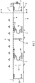
Fig. 1 is a schematic side view of a board assembly according to an embodiment of the present invention. -
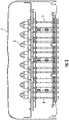
Fig. 2 is a cross-sectional view of the board assembly inFig. 1 together with a radome taken along the cross-sectional line A-A inFig. 1 . -
Fig. 3 is an exploded view of the board assembly inFig. 1 . -
Fig. 4 is a perspective view of a coaxial cable assembly of the board assembly inFig. 1 . - A board assembly according to an embodiment of the present invention and a base station antenna including the board assembly will be described below with reference to
Fig. 1 to Fig. 4 . The embodiments shown inFig. 1 to Fig. 4 are exemplary and do not limit the protection scope of the present invention. For example, a board assembly to be protected may have only a part of the board assembly as shown inFig. 1 to Fig. 3 . The board assembly may have a roughly rectangular profile. Similarly, the base station antenna may have a roughly rectangular profile. - The board assembly as shown in
Fig. 1 to Fig. 3 may include a reflector 1 and asupport backplate 2. The reflector 1 may be made of aluminum or an aluminum alloy plate, for example. Thesupport backplate 2 may be configured as a frame made of aluminum or an aluminum alloy plate, for example, or may also be a planar element. The board assembly includes afirst circuit board 3 and asecond circuit board 4. Thefirst circuit board 3 may be mounted on the reflector 1. Thesecond circuit board 4 may be mounted on thesupport backplate 2. Thefirst circuit board 3 may be a feeder panel. Thesecond circuit board 4 may be a calibration board. - The reflector 1 and the
support backplate 2 may be spaced apart from each other by at least one spacer, thus making thefirst circuit board 3 and thesecond circuit board 4 spaced apart from each other. As can be seen fromFig. 1 andFig. 3 , the board assembly may include two spacers composed of metal moldedmembers 11 and two rows of spacers composed ofplastic pillars 12, wherein, the two metal moldedmembers 11 are located outside and the twoplastic pillars 12 are located inside. The board assembly may include an array ofradiators 6, and theradiators 6 extend from the reflector 1 in a direction away from thesecond circuit board 4. - The
first circuit board 3 may have a plurality of firstelectrical connectors 13. Thesecond circuit board 4 may have a plurality of secondelectrical connectors 14. The firstelectrical connectors 13 and the secondelectrical connectors 14 are electrically connected by a plurality ofcoaxial cable assemblies 5. Eachcoaxial cable assembly 5 extends between thefirst circuit board 3 and thesecond circuit board 4. As shown inFig. 4 , thecoaxial cable assembly 5 may include acoaxial cable 8, a first correspondingelectrical connector 9 matching the firstelectrical connector 13 on a first end of thecoaxial cable 8, and a second correspondingelectrical connector 10 matching the secondelectrical connector 14 on a second end opposite to the first end on thecoaxial cable 8. The firstelectrical connectors 13 and the secondelectrical connectors 14, as well as the first correspondingelectrical connectors 9 and the second correspondingelectrical connectors 10 may be radio frequency connectors. These electrical connectors may be respectively arranged in an array according to the number of these electrical connectors and the space available on corresponding circuit boards. For example, it is possible that the first circuit board may have 2 × 8, 2 × 12, or 3 × 4 first electrical connectors. The number and arrangement of the second electrical connectors as well as the number and arrangement of the coaxial cable assemblies may correspond to the number and arrangement of the first electrical connectors. - In the embodiments shown in
Fig. 1 to Fig. 3 , the board assembly may include an array of 8 × 8radiators 6, two rows ofcoaxial cable assemblies 5, and two rows ofplastic pillars 12. The number of components involved is merely exemplary, and other numbers or different arrangements are also feasible. - It will be understood that, the terminology used herein is for the purpose of describing particular aspects only and is not intended to be limiting of the disclosure. As used herein, the singular forms "a", "an" and "the" are intended to include the plural forms as well, unless the context clearly indicates otherwise. It will be further understood that the terms "comprise" and "include" (and variants thereof), when used in this specification, specify the presence of stated operations, elements, and/or components, but do not preclude the presence or addition of one or more other operations, elements, components, and/or groups thereof. As used herein, the term "and/or" includes any and all combinations of one or more of the associated listed items. Like reference numbers signify like elements throughout the description of the figures.
- The thicknesses of elements in the drawings may be exaggerated for the sake of clarity. Further, it will be understood that when an element is referred to as being "on," "coupled to" or "connected to" another element, the element may be formed directly on, coupled to or connected to the other element, or there may be one or more intervening elements therebetween. In contrast, terms such as "directly on," "directly coupled to" and "directly connected to," when used herein, indicate that no intervening elements are present. Other words used to describe the relationship between elements should be interpreted in a like fashion (i.e., "between" versus "directly between", "attached" versus "directly attached," "adjacent" versus "directly adjacent", etc.).
- Terms such as "top," "bottom," "upper," "lower," "above," "below," and the like are used herein to describe the relationship of one element, layer or region to another element, layer or region as illustrated in the figures. It will be understood that these terms are intended to encompass different orientations of the device in addition to the orientation depicted in the figures.
- It will be understood that, although the terms "first," "second," etc. may be used herein to describe various elements, these elements should not be limited by these terms. These terms are only used to distinguish one element from another. Thus, a first element could be termed a second element without departing from the teachings of the inventive concept.
- It will also be appreciated that all example embodiments disclosed herein can be combined in any way.
- Finally, it is to be noted that, the above-described embodiments are merely for understanding the present invention but not constitute a limit on the protection scope of the present invention. For those skilled in the art, modifications may be made on the basis of the above-described embodiments, and these modifications do not depart from the protection scope of the present invention.
Claims (10)
- A board assembly used for a base station antenna, the board assembly including a first circuit board (3) and a second circuit board (4), wherein, the first circuit board and the second circuit board are spaced apart from each other, the first circuit board has a plurality of first electrical connectors (13), the second circuit board has a plurality of second electrical connectors (14), the first electrical connectors and the second electrical connectors are electrically connected by a plurality of coaxial cable assemblies (5), each coaxial cable assembly extends between the first circuit board and the second circuit board, and includes a coaxial cable (8), a first corresponding electrical connector (9) matching the first electrical connector on a first end of the coaxial cable, and a second corresponding electrical connector (10) matching the second electrical connector on a second end opposite to the first end on the coaxial cable.
- The board assembly used for a base station antenna according to claim 1, wherein, the board assembly includes a reflector (1), and the first circuit board is mounted on the reflector.
- The board assembly used for a base station antenna according to either claim 1 or claim 2, wherein, the board assembly includes a support backplate (2), and the second circuit board is mounted on the support backplate.
- The board assembly used for a base station antenna according to either claim 1 or claim 2, wherein, the board assembly includes a support backplate, the second circuit board is mounted on the support backplate, and the reflector and the support backplate are spaced apart from each other by at least one spacer, thus making the first circuit board and the second circuit board spaced apart from each other.
- The board assembly used for a base station antenna according to any of claims 1 to 4, wherein, the board assembly includes at least one spacer composed of a metal molded member (11) and/or at least one spacer composed of a plastic pillar (12).
- The board assembly used for a base station antenna according to any one of the preceding claims, wherein, the board assembly includes an array of radiators (6), and the radiators extend from the reflector in a direction away from the second circuit board.
- The board assembly used for a base station antenna according to any one of the preceding claims, wherein, the first electrical connectors and the second electrical connectors, as well as the first corresponding electrical connectors and the second corresponding electrical connectors are radio frequency connectors.
- The board assembly used for a base station antenna according to any one of the preceding claims, wherein, the first electrical connectors and the second electrical connectors, as well as the first corresponding electrical connectors and the second corresponding electrical connectors are respectively arranged in an array.
- The board assembly used for a base station antenna according to any one of the preceding claims, wherein, the first circuit board is a feeder panel, and the second circuit board is a calibration board.
- A base station antenna, including a radome and a board assembly accommodated in the radome, wherein, the board assembly is a board assembly used for a base station antenna according to any one of claims 1 to 9.
Applications Claiming Priority (1)
| Application Number | Priority Date | Filing Date | Title |
|---|---|---|---|
| CN202023099546.7U CN213460078U (en) | 2020-12-21 | 2020-12-21 | Base station antenna and board assembly for base station antenna |
Publications (2)
| Publication Number | Publication Date |
|---|---|
| EP4016730A1 true EP4016730A1 (en) | 2022-06-22 |
| EP4016730B1 EP4016730B1 (en) | 2025-04-02 |
Family
ID=76305531
Family Applications (1)
| Application Number | Title | Priority Date | Filing Date |
|---|---|---|---|
| EP21209848.7A Active EP4016730B1 (en) | 2020-12-21 | 2021-11-23 | Base station antenna and board assembly for base station antenna |
Country Status (4)
| Country | Link |
|---|---|
| US (1) | US11728565B2 (en) |
| EP (1) | EP4016730B1 (en) |
| CN (1) | CN213460078U (en) |
| FI (1) | FI4016730T3 (en) |
Families Citing this family (1)
| Publication number | Priority date | Publication date | Assignee | Title |
|---|---|---|---|---|
| WO2022067486A1 (en) * | 2020-09-29 | 2022-04-07 | Telefonaktiebolaget Lm Ericsson (Publ) | Base station |
Citations (5)
| Publication number | Priority date | Publication date | Assignee | Title |
|---|---|---|---|---|
| US20130070819A1 (en) * | 2009-05-26 | 2013-03-21 | Huawei Technologies Co., Ltd. | Antenna device |
| US20140139393A1 (en) * | 2012-11-16 | 2014-05-22 | Samsung Electronics Co., Ltd | Electronic device including antenna |
| US20180006363A1 (en) * | 2015-03-16 | 2018-01-04 | Kmw Inc. | Signal distributing/combining apparatus in antenna apparatus of mobile communication base station |
| CN107799896A (en) * | 2017-11-24 | 2018-03-13 | 广东博纬通信科技有限公司 | A kind of TD LTE smart antennas for applying to frequency range near 3500MHz |
| US20200259248A1 (en) * | 2017-10-30 | 2020-08-13 | Huawei Technologies Co., Ltd. | Antenna, antenna assembly, and base station |
Family Cites Families (2)
| Publication number | Priority date | Publication date | Assignee | Title |
|---|---|---|---|---|
| JP2013197968A (en) * | 2012-03-21 | 2013-09-30 | Hitachi Cable Ltd | Antenna modem and antenna control system |
| US10639123B2 (en) | 2016-07-06 | 2020-05-05 | Medtronic Vascular, Inc. | Biomatter capture mechanism and method |
-
2020
- 2020-12-21 CN CN202023099546.7U patent/CN213460078U/en active Active
-
2021
- 2021-10-28 US US17/513,087 patent/US11728565B2/en active Active
- 2021-11-23 EP EP21209848.7A patent/EP4016730B1/en active Active
- 2021-11-23 FI FIEP21209848.7T patent/FI4016730T3/en active
Patent Citations (5)
| Publication number | Priority date | Publication date | Assignee | Title |
|---|---|---|---|---|
| US20130070819A1 (en) * | 2009-05-26 | 2013-03-21 | Huawei Technologies Co., Ltd. | Antenna device |
| US20140139393A1 (en) * | 2012-11-16 | 2014-05-22 | Samsung Electronics Co., Ltd | Electronic device including antenna |
| US20180006363A1 (en) * | 2015-03-16 | 2018-01-04 | Kmw Inc. | Signal distributing/combining apparatus in antenna apparatus of mobile communication base station |
| US20200259248A1 (en) * | 2017-10-30 | 2020-08-13 | Huawei Technologies Co., Ltd. | Antenna, antenna assembly, and base station |
| CN107799896A (en) * | 2017-11-24 | 2018-03-13 | 广东博纬通信科技有限公司 | A kind of TD LTE smart antennas for applying to frequency range near 3500MHz |
Non-Patent Citations (1)
| Title |
|---|
| ADITHYA ANGAMPALLY HARI ET AL: "Experimental evaluation of a beamforming array calibration system", 2014 IEEE AEROSPACE CONFERENCE, IEEE, 1 March 2014 (2014-03-01), pages 1 - 7, XP032607422, DOI: 10.1109/AERO.2014.6836524 * |
Also Published As
| Publication number | Publication date |
|---|---|
| US11728565B2 (en) | 2023-08-15 |
| FI4016730T3 (en) | 2025-05-19 |
| EP4016730B1 (en) | 2025-04-02 |
| US20220200135A1 (en) | 2022-06-23 |
| CN213460078U (en) | 2021-06-15 |
Similar Documents
| Publication | Publication Date | Title |
|---|---|---|
| US12046813B2 (en) | Antenna filter unit, and radio unit | |
| US11108138B2 (en) | Antenna system and assembly method thereof, and base-station array antenna | |
| CN1577974B (en) | Antenna element, feed probe, dielectric spacer, antenna and method of communicating with a plurality of devices | |
| US8072384B2 (en) | Dual-polarized antenna modules | |
| KR101095139B1 (en) | Reflector for Wireless Mobile Antenna | |
| US20220037753A1 (en) | Base station antennas having double-sided phase shifters and/or rearwardly extending phase shifters and associated phase shifter assemblies | |
| US20100265150A1 (en) | Antenna Assembly | |
| US20190044258A1 (en) | Cable connector block assemblies for base station antennas | |
| US20210126351A1 (en) | Integrated active antennas suitable for massive mimo operation | |
| US12374770B2 (en) | Base station antennas having an active antenna module(s) and related mounting systems and methods | |
| US20200412010A1 (en) | Lightweight antenna unit, lightweight array antenna, and assembly method for antenna unit | |
| US20140139393A1 (en) | Electronic device including antenna | |
| US11342661B2 (en) | Antenna structure and wireless communication device using the same | |
| EP2819240A1 (en) | Tube and ring directional end-fire array antenna | |
| US20060109193A1 (en) | Base station panel antenna with dual-polarized radiating elements and shaped reflector | |
| EP4016730B1 (en) | Base station antenna and board assembly for base station antenna | |
| US20110273352A1 (en) | Antenna Structure | |
| CN102474003B (en) | Antenna device | |
| EP3639508B1 (en) | A communcation device and a method for assembling a communication device | |
| US10938112B1 (en) | Antenna and mobile terminal | |
| KR102821048B1 (en) | Antenna with filter unit and antenna device the same | |
| CN117996446A (en) | Feed network, phase shifter and antenna device | |
| US20090303151A1 (en) | Low profile gps antenna assembly | |
| CN114221125A (en) | Integrated antenna unit and antenna device | |
| CN212257687U (en) | Flat antenna |
Legal Events
| Date | Code | Title | Description |
|---|---|---|---|
| PUAI | Public reference made under article 153(3) epc to a published international application that has entered the european phase |
Free format text: ORIGINAL CODE: 0009012 |
|
| STAA | Information on the status of an ep patent application or granted ep patent |
Free format text: STATUS: REQUEST FOR EXAMINATION WAS MADE |
|
| 17P | Request for examination filed |
Effective date: 20211123 |
|
| AK | Designated contracting states |
Kind code of ref document: A1 Designated state(s): AL AT BE BG CH CY CZ DE DK EE ES FI FR GB GR HR HU IE IS IT LI LT LU LV MC MK MT NL NO PL PT RO RS SE SI SK SM TR |
|
| RAP3 | Party data changed (applicant data changed or rights of an application transferred) |
Owner name: COMMSCOPE TECHNOLOGIES LLC |
|
| RAP1 | Party data changed (applicant data changed or rights of an application transferred) |
Owner name: OUTDOOR WIRELESS NETWORKS LLC |
|
| GRAP | Despatch of communication of intention to grant a patent |
Free format text: ORIGINAL CODE: EPIDOSNIGR1 |
|
| RIC1 | Information provided on ipc code assigned before grant |
Ipc: H01R 24/50 20110101ALN20240923BHEP Ipc: H01R 24/52 20110101ALN20240923BHEP Ipc: H01Q 21/08 20060101ALI20240923BHEP Ipc: H01Q 1/24 20060101AFI20240923BHEP |
|
| STAA | Information on the status of an ep patent application or granted ep patent |
Free format text: STATUS: GRANT OF PATENT IS INTENDED |
|
| INTG | Intention to grant announced |
Effective date: 20241030 |
|
| RIN1 | Information on inventor provided before grant (corrected) |
Inventor name: WEN, HANGSHENG Inventor name: TANG, PULIANG Inventor name: NIE, CHENGGUO Inventor name: ZHANG, XUN Inventor name: SU, RUIXIN |
|
| GRAS | Grant fee paid |
Free format text: ORIGINAL CODE: EPIDOSNIGR3 |
|
| GRAA | (expected) grant |
Free format text: ORIGINAL CODE: 0009210 |
|
| STAA | Information on the status of an ep patent application or granted ep patent |
Free format text: STATUS: THE PATENT HAS BEEN GRANTED |
|
| AK | Designated contracting states |
Kind code of ref document: B1 Designated state(s): AL AT BE BG CH CY CZ DE DK EE ES FI FR GB GR HR HU IE IS IT LI LT LU LV MC MK MT NL NO PL PT RO RS SE SI SK SM TR |
|
| REG | Reference to a national code |
Ref country code: GB Ref legal event code: FG4D |
|
| REG | Reference to a national code |
Ref country code: CH Ref legal event code: EP |
|
| REG | Reference to a national code |
Ref country code: IE Ref legal event code: FG4D |
|
| REG | Reference to a national code |
Ref country code: DE Ref legal event code: R096 Ref document number: 602021028454 Country of ref document: DE |
|
| REG | Reference to a national code |
Ref country code: FI Ref legal event code: FGE |
|
| REG | Reference to a national code |
Ref country code: SE Ref legal event code: TRGR |
|
| REG | Reference to a national code |
Ref country code: NL Ref legal event code: MP Effective date: 20250402 |
|
| PG25 | Lapsed in a contracting state [announced via postgrant information from national office to epo] |
Ref country code: NL Free format text: LAPSE BECAUSE OF FAILURE TO SUBMIT A TRANSLATION OF THE DESCRIPTION OR TO PAY THE FEE WITHIN THE PRESCRIBED TIME-LIMIT Effective date: 20250402 |
|
| REG | Reference to a national code |
Ref country code: AT Ref legal event code: MK05 Ref document number: 1782252 Country of ref document: AT Kind code of ref document: T Effective date: 20250402 |
|
| PG25 | Lapsed in a contracting state [announced via postgrant information from national office to epo] |
Ref country code: PT Free format text: LAPSE BECAUSE OF FAILURE TO SUBMIT A TRANSLATION OF THE DESCRIPTION OR TO PAY THE FEE WITHIN THE PRESCRIBED TIME-LIMIT Effective date: 20250804 Ref country code: ES Free format text: LAPSE BECAUSE OF FAILURE TO SUBMIT A TRANSLATION OF THE DESCRIPTION OR TO PAY THE FEE WITHIN THE PRESCRIBED TIME-LIMIT Effective date: 20250402 |
|
| REG | Reference to a national code |
Ref country code: LT Ref legal event code: MG9D |
|
| PG25 | Lapsed in a contracting state [announced via postgrant information from national office to epo] |
Ref country code: NO Free format text: LAPSE BECAUSE OF FAILURE TO SUBMIT A TRANSLATION OF THE DESCRIPTION OR TO PAY THE FEE WITHIN THE PRESCRIBED TIME-LIMIT Effective date: 20250702 Ref country code: GR Free format text: LAPSE BECAUSE OF FAILURE TO SUBMIT A TRANSLATION OF THE DESCRIPTION OR TO PAY THE FEE WITHIN THE PRESCRIBED TIME-LIMIT Effective date: 20250703 |
|
| PG25 | Lapsed in a contracting state [announced via postgrant information from national office to epo] |
Ref country code: PL Free format text: LAPSE BECAUSE OF FAILURE TO SUBMIT A TRANSLATION OF THE DESCRIPTION OR TO PAY THE FEE WITHIN THE PRESCRIBED TIME-LIMIT Effective date: 20250402 |
|
| PG25 | Lapsed in a contracting state [announced via postgrant information from national office to epo] |
Ref country code: BG Free format text: LAPSE BECAUSE OF FAILURE TO SUBMIT A TRANSLATION OF THE DESCRIPTION OR TO PAY THE FEE WITHIN THE PRESCRIBED TIME-LIMIT Effective date: 20250402 |
|
| PG25 | Lapsed in a contracting state [announced via postgrant information from national office to epo] |
Ref country code: HR Free format text: LAPSE BECAUSE OF FAILURE TO SUBMIT A TRANSLATION OF THE DESCRIPTION OR TO PAY THE FEE WITHIN THE PRESCRIBED TIME-LIMIT Effective date: 20250402 |
|
| PG25 | Lapsed in a contracting state [announced via postgrant information from national office to epo] |
Ref country code: AT Free format text: LAPSE BECAUSE OF FAILURE TO SUBMIT A TRANSLATION OF THE DESCRIPTION OR TO PAY THE FEE WITHIN THE PRESCRIBED TIME-LIMIT Effective date: 20250402 |
|
| PG25 | Lapsed in a contracting state [announced via postgrant information from national office to epo] |
Ref country code: RS Free format text: LAPSE BECAUSE OF FAILURE TO SUBMIT A TRANSLATION OF THE DESCRIPTION OR TO PAY THE FEE WITHIN THE PRESCRIBED TIME-LIMIT Effective date: 20250702 |
|
| PG25 | Lapsed in a contracting state [announced via postgrant information from national office to epo] |
Ref country code: IS Free format text: LAPSE BECAUSE OF FAILURE TO SUBMIT A TRANSLATION OF THE DESCRIPTION OR TO PAY THE FEE WITHIN THE PRESCRIBED TIME-LIMIT Effective date: 20250802 |
|
| PG25 | Lapsed in a contracting state [announced via postgrant information from national office to epo] |
Ref country code: LV Free format text: LAPSE BECAUSE OF FAILURE TO SUBMIT A TRANSLATION OF THE DESCRIPTION OR TO PAY THE FEE WITHIN THE PRESCRIBED TIME-LIMIT Effective date: 20250402 |
|
| REG | Reference to a national code |
Ref country code: DE Ref legal event code: R097 Ref document number: 602021028454 Country of ref document: DE |
|
| PG25 | Lapsed in a contracting state [announced via postgrant information from national office to epo] |
Ref country code: SM Free format text: LAPSE BECAUSE OF FAILURE TO SUBMIT A TRANSLATION OF THE DESCRIPTION OR TO PAY THE FEE WITHIN THE PRESCRIBED TIME-LIMIT Effective date: 20250402 Ref country code: DK Free format text: LAPSE BECAUSE OF FAILURE TO SUBMIT A TRANSLATION OF THE DESCRIPTION OR TO PAY THE FEE WITHIN THE PRESCRIBED TIME-LIMIT Effective date: 20250402 |
|
| PGFP | Annual fee paid to national office [announced via postgrant information from national office to epo] |
Ref country code: FI Payment date: 20251125 Year of fee payment: 5 |
|
| PGFP | Annual fee paid to national office [announced via postgrant information from national office to epo] |
Ref country code: SE Payment date: 20251127 Year of fee payment: 5 |
|
| PG25 | Lapsed in a contracting state [announced via postgrant information from national office to epo] |
Ref country code: CZ Free format text: LAPSE BECAUSE OF FAILURE TO SUBMIT A TRANSLATION OF THE DESCRIPTION OR TO PAY THE FEE WITHIN THE PRESCRIBED TIME-LIMIT Effective date: 20250402 |
|
| PG25 | Lapsed in a contracting state [announced via postgrant information from national office to epo] |
Ref country code: EE Free format text: LAPSE BECAUSE OF FAILURE TO SUBMIT A TRANSLATION OF THE DESCRIPTION OR TO PAY THE FEE WITHIN THE PRESCRIBED TIME-LIMIT Effective date: 20250402 |
|
| PG25 | Lapsed in a contracting state [announced via postgrant information from national office to epo] |
Ref country code: RO Free format text: LAPSE BECAUSE OF FAILURE TO SUBMIT A TRANSLATION OF THE DESCRIPTION OR TO PAY THE FEE WITHIN THE PRESCRIBED TIME-LIMIT Effective date: 20250402 Ref country code: SK Free format text: LAPSE BECAUSE OF FAILURE TO SUBMIT A TRANSLATION OF THE DESCRIPTION OR TO PAY THE FEE WITHIN THE PRESCRIBED TIME-LIMIT Effective date: 20250402 |
|
| PG25 | Lapsed in a contracting state [announced via postgrant information from national office to epo] |
Ref country code: IT Free format text: LAPSE BECAUSE OF FAILURE TO SUBMIT A TRANSLATION OF THE DESCRIPTION OR TO PAY THE FEE WITHIN THE PRESCRIBED TIME-LIMIT Effective date: 20250402 |
|
| PLBE | No opposition filed within time limit |
Free format text: ORIGINAL CODE: 0009261 |
|
| STAA | Information on the status of an ep patent application or granted ep patent |
Free format text: STATUS: NO OPPOSITION FILED WITHIN TIME LIMIT |
|
| REG | Reference to a national code |
Ref country code: CH Ref legal event code: L10 Free format text: ST27 STATUS EVENT CODE: U-0-0-L10-L00 (AS PROVIDED BY THE NATIONAL OFFICE) Effective date: 20260211 |
|
| 26N | No opposition filed |
Effective date: 20260105 |
|
| REG | Reference to a national code |
Ref country code: DE Ref legal event code: R119 Ref document number: 602021028454 Country of ref document: DE |
|
| REG | Reference to a national code |
Ref country code: CH Ref legal event code: H13 Free format text: ST27 STATUS EVENT CODE: U-0-0-H10-H13 (AS PROVIDED BY THE NATIONAL OFFICE) Effective date: 20260623 |
|
| PG25 | Lapsed in a contracting state [announced via postgrant information from national office to epo] |
Ref country code: LT Free format text: LAPSE BECAUSE OF FAILURE TO SUBMIT A TRANSLATION OF THE DESCRIPTION OR TO PAY THE FEE WITHIN THE PRESCRIBED TIME-LIMIT Effective date: 20250402 |
|
| PG25 | Lapsed in a contracting state [announced via postgrant information from national office to epo] |
Ref country code: MC Free format text: LAPSE BECAUSE OF FAILURE TO SUBMIT A TRANSLATION OF THE DESCRIPTION OR TO PAY THE FEE WITHIN THE PRESCRIBED TIME-LIMIT Effective date: 20250402 |
|
| PG25 | Lapsed in a contracting state [announced via postgrant information from national office to epo] |
Ref country code: LU Free format text: LAPSE BECAUSE OF NON-PAYMENT OF DUE FEES Effective date: 20251123 Ref country code: CH Free format text: LAPSE BECAUSE OF NON-PAYMENT OF DUE FEES Effective date: 20251130 |