EP4016614A1 - Method of manufacturing multi-die semiconductor devices - Google Patents
Method of manufacturing multi-die semiconductor devices Download PDFInfo
- Publication number
- EP4016614A1 EP4016614A1 EP21214666.6A EP21214666A EP4016614A1 EP 4016614 A1 EP4016614 A1 EP 4016614A1 EP 21214666 A EP21214666 A EP 21214666A EP 4016614 A1 EP4016614 A1 EP 4016614A1
- Authority
- EP
- European Patent Office
- Prior art keywords
- electrically
- lines
- laser
- conductive
- subset
- Prior art date
- Legal status (The legal status is an assumption and is not a legal conclusion. Google has not performed a legal analysis and makes no representation as to the accuracy of the status listed.)
- Granted
Links
Images


Classifications
-
- H—ELECTRICITY
- H10—SEMICONDUCTOR DEVICES; ELECTRIC SOLID-STATE DEVICES NOT OTHERWISE PROVIDED FOR
- H10W—GENERIC PACKAGES, INTERCONNECTIONS, CONNECTORS OR OTHER CONSTRUCTIONAL DETAILS OF DEVICES COVERED BY CLASS H10
- H10W70/00—Package substrates; Interposers; Redistribution layers [RDL]
- H10W70/40—Leadframes
- H10W70/464—Additional interconnections in combination with leadframes
-
- H—ELECTRICITY
- H10—SEMICONDUCTOR DEVICES; ELECTRIC SOLID-STATE DEVICES NOT OTHERWISE PROVIDED FOR
- H10W—GENERIC PACKAGES, INTERCONNECTIONS, CONNECTORS OR OTHER CONSTRUCTIONAL DETAILS OF DEVICES COVERED BY CLASS H10
- H10W70/00—Package substrates; Interposers; Redistribution layers [RDL]
- H10W70/01—Manufacture or treatment
- H10W70/04—Manufacture or treatment of leadframes
- H10W70/048—Mechanical treatments, e.g. punching, cutting, deforming or cold welding
-
- H—ELECTRICITY
- H10—SEMICONDUCTOR DEVICES; ELECTRIC SOLID-STATE DEVICES NOT OTHERWISE PROVIDED FOR
- H10W—GENERIC PACKAGES, INTERCONNECTIONS, CONNECTORS OR OTHER CONSTRUCTIONAL DETAILS OF DEVICES COVERED BY CLASS H10
- H10W70/00—Package substrates; Interposers; Redistribution layers [RDL]
- H10W70/01—Manufacture or treatment
- H10W70/04—Manufacture or treatment of leadframes
- H10W70/041—Connecting or disconnecting interconnections to or from leadframes, e.g. connecting bond wires or bumps
-
- H—ELECTRICITY
- H10—SEMICONDUCTOR DEVICES; ELECTRIC SOLID-STATE DEVICES NOT OTHERWISE PROVIDED FOR
- H10W—GENERIC PACKAGES, INTERCONNECTIONS, CONNECTORS OR OTHER CONSTRUCTIONAL DETAILS OF DEVICES COVERED BY CLASS H10
- H10W70/00—Package substrates; Interposers; Redistribution layers [RDL]
- H10W70/40—Leadframes
- H10W70/411—Chip-supporting parts, e.g. die pads
-
- H—ELECTRICITY
- H10—SEMICONDUCTOR DEVICES; ELECTRIC SOLID-STATE DEVICES NOT OTHERWISE PROVIDED FOR
- H10W—GENERIC PACKAGES, INTERCONNECTIONS, CONNECTORS OR OTHER CONSTRUCTIONAL DETAILS OF DEVICES COVERED BY CLASS H10
- H10W74/00—Encapsulations, e.g. protective coatings
- H10W74/01—Manufacture or treatment
- H10W74/016—Manufacture or treatment using moulds
-
- H—ELECTRICITY
- H10—SEMICONDUCTOR DEVICES; ELECTRIC SOLID-STATE DEVICES NOT OTHERWISE PROVIDED FOR
- H10W—GENERIC PACKAGES, INTERCONNECTIONS, CONNECTORS OR OTHER CONSTRUCTIONAL DETAILS OF DEVICES COVERED BY CLASS H10
- H10W74/00—Encapsulations, e.g. protective coatings
- H10W74/10—Encapsulations, e.g. protective coatings characterised by their shape or disposition
- H10W74/111—Encapsulations, e.g. protective coatings characterised by their shape or disposition the semiconductor body being completely enclosed
-
- H—ELECTRICITY
- H10—SEMICONDUCTOR DEVICES; ELECTRIC SOLID-STATE DEVICES NOT OTHERWISE PROVIDED FOR
- H10W—GENERIC PACKAGES, INTERCONNECTIONS, CONNECTORS OR OTHER CONSTRUCTIONAL DETAILS OF DEVICES COVERED BY CLASS H10
- H10W90/00—Package configurations
- H10W90/811—Multiple chips on leadframes
Definitions
- the description relates to multi-die or multi-chip semiconductor devices which may be suitable for use in various areas such as the automotive, industrial and/or consumer electronics sectors.
- Conventional packaged multi-die semiconductor devices may comprise:
- each semiconductor die may be electrically coupled to one or more of the other semiconductor dice (e.g., to transmit and/or receive signals) by means of so-called die-to-die interconnections.
- die-to-die interconnections can be implemented by means of wire bonding, with bonding wires also encapsulated in the plastics package, or by electroless plating, or by selectively dispensing an electrically conductive paste (e.g., a silver paste) to form an electrically conductive track.
- die-to-die interconnections by means of wire bonding, electroless plating or dispensation of a conductive paste may lead to high manufacturing costs and/or a low reliability of the die-to-die interconnections.
- An object of one or more embodiments is to contribute in providing such improved die-to-die interconnections in multi-die semiconductor devices.
- such an object can be achieved by means of a method of manufacturing a multi-die semiconductor device having the features set forth in the claims that follow.
- a metallic leadframe which includes a die pad and a set of electrically-conductive leads arranged around the die pad.
- a set of semiconductor dice is arranged onto the die pad, the set of semiconductor dice including at least a first semiconductor die and a second semiconductor die.
- the first semiconductor die and the second semiconductor die comprise respective sets of bonding pads at their front surfaces opposed to the die pad.
- a layer of laser-activatable material e.g., a plastic material
- is formed is formed (e.g., molded) onto the first semiconductor die, the second semiconductor die and the set of electrically-conductive leads.
- Laser radiation is directed onto the laser-activatable material to pattern a set of laser-activated lines, wherein the set of laser-activated lines includes a first subset of laser-activated lines configured to couple selected bonding pads of the first semiconductor die and/or the second semiconductor die to selected electrically-conductive leads in the set of electrically-conductive leads, a second subset of laser-activated lines configured to couple selected bonding pads of the first semiconductor die to selected bonding pads of the second semiconductor die, and a third subset of laser-activated lines configured to couple each of the laser-activated lines in the second subset of laser-activated lines to at least one laser-activated line in the first subset of laser-activated lines, and/or to at least one electrically-conductive lead in the set of electrically-conductive leads.
- the set of laser-activated lines includes a first subset of laser-activated lines configured to couple selected bonding pads of the first semiconductor die and/or the second semiconductor die to selected electrically-conductive leads in the set of electrically-conductive leads, a second
- a first metallic layer is deposited onto the first, second and third subsets of laser-activated lines to provide respective first, second and third subsets of electrically-conductive lines.
- a second metallic layer is selectively deposited onto the first and second subsets of electrically-conductive lines by means of electroplating to provide respective first and second subsets of electrically-conductive tracks. The electrically-conductive lines in the third subset of electrically-conductive lines are then selectively removed.
- One or more embodiments may thus facilitate forming electrically floating metallic tracks (e.g., die-to-die interconnections) in a multi-die semiconductor device by means of a Laser Direct Structuring (LDS) process and a subsequent electroplating process, by forming temporary "tie-bars" which connect the electrically floating pattern regions to an electrically grounded region, and subsequently removing the temporary tie-bars.
- LDS Laser Direct Structuring
- references to "an embodiment” or “one embodiment” in the framework of the present description is intended to indicate that a particular configuration, structure, or characteristic described in relation to the embodiment is comprised in at least one embodiment.
- phrases such as “in an embodiment” or “in one embodiment” that may be present in one or more points of the present description do not necessarily refer to one and the same embodiment.
- particular conformations, structures, or characteristics may be combined in any adequate way in one or more embodiments.
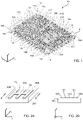
- Figure 1 is a perspective view exemplary of certain internal components of a multi-die semiconductor device 10 comprising two semiconductor dice.
- the semiconductor device 10 exemplified herein comprises a flat no-leads package (e.g., a QFN package).
- the multi-die semiconductor device 10 comprises a metallic leadframe including a die pad 100 and a plurality of electrically-conductive leads 102 arranged around the die pad 100.
- a first semiconductor die 12 and a second semiconductor die 14 are arranged on the die pad 100, e.g., attached by means of die attach material such as a glue.
- a package P of plastic material (here shown in transparency and with dashed lines for the sake of illustration only) encapsulates the semiconductor dice 12, 14 arranged on the die pad 100 and at least a portion of the electrically-conductive leads 102 facing towards the die pad 100.
- the front (e.g., upper or top) surfaces of the semiconductor dice 12 and 14, i.e., the surfaces which are opposed to the die pad 100, are provided with bonding pads for electrically coupling the semiconductor dice 12, 14 to the leads 102 and/or between themselves.
- bonding pads for electrically coupling the semiconductor dice 12, 14 to the leads 102 and/or between themselves.
- LDS Laser Direct Structuring
- a metallic inorganic compound activatable by means of laser radiation may be provided in the plastic material used for molding the package P (or at least a portion of the package P which is in contact with the semiconductor dice 12, 14).
- Laser radiation may then be directed onto the plastic material to pattern the course of the later circuit trace on and in the laser-activatable plastic material.
- the metal additive forms a laser-activated (e.g., micro-rough) track or line.
- the metal particles of this laser-activated track or line form the nuclei for a subsequent metallization step which will grow an electrically-conductive track on the laser-activated plastic material.
- Such a metallization step may comprise an electroless plating step (e.g., in a copper bath). Electroless plating may turn out to be disadvantageous, insofar as it may require long plating times in order to deposit a sufficiently thick metallic layer to provide satisfactory electrical conductivity for the die-to-die and die-to-lead interconnections 16A, 16B, 16C.
- the metallization step may comprise an electroplating step (or galvanic deposition step).
- an electroplating step is suitable for plating only those laser-activated tracks which provide a continuous electrical path towards a ground terminal during the electroplating process. Since the ground terminal is typically applied to the metallic leadframe, in a conventional manufacturing process the electroplating step would be suitable only for manufacturing die-to-lead interconnections such as the interconnections 16A, 16C and 16C' exemplified in Figure 1 .
- the electroplating step would not be suitable for manufacturing conventional die-to-die interconnections 16B and 16B', insofar as the die-to-die interconnections are electrically floating, i.e., they do not provide a continuous current path towards ground (e.g., towards the leadframe, in particular towards the electrically-conductive leads 102).
- One or more embodiments of the present description relate to a manufacturing method which facilitates growing die-to-die metallic interconnections in a multi-die semiconductor device by means of an electroplating step.
- a manufacturing method may comprise the conventional steps of providing a metallic leadframe including a die pad 100 and a set of electrically-conductive leads 102 arranged around the die pad, and arranging (e.g., attaching by means of a die attach material such as a glue) a set of semiconductor dice 12, 14 onto the die pad.
- the set of semiconductor dice may include a first semiconductor die 12 and a second semiconductor die 14, but the number of semiconductor dice may vary in different embodiments (e.g., up to five, ten or possibly more dice in the same packaged semiconductor device).
- the semiconductor dice 12, 14 comprise respective sets of bonding pads at their front (e.g., upper or top) surfaces.
- a method according to one or more embodiments may further comprise the step of providing (e.g., molding) a layer of laser-activatable material 200 (e.g., a plastic material suitable for carrying out an LDS process) onto the semiconductor dice 12, 14 and the leads 102.
- the laser-activatable material 200 may be embedded in the molding compound which provides the package P.
- the catalytic (metallic) particles in the laser-activatable material 200 may have a size in the range of 0.5 ⁇ m to 2 ⁇ m.
- a method according to one or more embodiments may comprise the step of directing laser radiation onto the laser-activatable material 200 to pattern a set of laser-activated lines, which will be used as "seed" lines for one or more subsequent plating steps.
- the set of laser-activated patterned lines may include:
- the laser-activated lines may not only extend at the surface of the material 200, but may also extend through the material 200 in order to provide vertical vias which allow to establish connection with the bonding pads provided at the front surfaces of the semiconductor dice 12, 14 and/or with the leads 102.
- a method according to one or more embodiments may further comprise the step of depositing (e.g., growing) by electroless plating a thin metallic layer (e.g., a copper layer) onto the first, second and third subsets of laser-activated patterned lines to provide respective first, second and third subsets of electrically-conductive lines.
- a thin metallic layer e.g., a copper layer
- such a thin metallic layer may have a thickness in the range of 1 ⁇ m to 10 ⁇ m, optionally equal to 5 ⁇ m.
- Figures 2A and 2B are exemplary of such electrically-conductive lines provided on the LDS material 200 after an electroless plating step.
- Figure 2A is a perspective view (taken along line I-I of Figure 1 and reproduced on an enlarged scale) of the LDS material and the electrically-conductive lines in a region between the semiconductor dice 12 and 14, and
- Figure 2B is a cross-sectional view taken along line II-II of Figure 2A in the y-z plane. It will be noted that such Figures, as well as the other Figures annexed herein, are not necessarily drawn to scale.
- electrically-conductive lines 160C may be provided which couple the bonding pads of the semiconductor dice 12, 14 to the leads 102 (see again the corresponding interconnection 16C' in Figure 1 ), and electrically-conductive lines 160B may be provided which couple the bonding pads of a semiconductor die 12 to the bonding pads of another semiconductor die 14 (see again the corresponding interconnection 16B' in Figure 1 ).
- the laser activation step and the electroless plating step may additionally provide electrically-conductive lines 162 which couple each of the electrically-floating lines 160B to at least one line 160C and/or to at least one lead 102 (i.e., providing temporary "tie-bars" which allow coupling the otherwise electrically-floating lines 160B to the leadframe).
- a method according to one or more embodiments may further comprise the step of selectively depositing (e.g., growing) by means of an electroplating process a thick metallic layer (e.g., a further copper layer) onto the electrically-conductive lines 160B and 160C to provide electrically-conductive tracks which implement respectively the interconnects 16A, 16B, 16B', 16C, and 16C'.
- a thick metallic layer may have a thickness in the range of 50 ⁇ m to 60 ⁇ m, optionally equal to 55 ⁇ m.
- a selective metal deposition by electroplating may be carried out, for instance, by providing a masking layer 300 which covers the "sacrificial" electrically-conductive lines 162, as exemplified in Figures 3A and 3B .
- a masking layer may comprise a photoresist material patterned by means of conventional photolithographic techniques, and/or any type of resist material selectively deposited onto the sacrificial electrically-conductive lines 162 by means of additive deposition techniques, such as ink-jet printing.
- an electroplating step may be carried out as exemplified in Figures 4A, 4B and 4C , so that a thick metallic layer is deposited onto the electrically-conductive lines 160B and 160C to provide the interconnects 16A, 16B, 16B', 16C, and 16C'.
- Figure 4C corresponds substantially to Figure 4B , but it emphasizes the different thicknesses of the thin, electroless-deposited metallic layer comprising the lines 160B, 160C and 162, and the thicker, electroplated metallic layer implementing the tracks 16B' and 16C'.
- the thickness of the masking layer 300 may be selected to be equal to or higher than the desired thickness of the interconnects 16A, 16B, 16B', 16C, and 16C', so that the electroplating step may be stopped when the thickness of the electrodeposited metal layer is equal to or lower than the thickness of the masking layer 300. In this way, "lateral" growth of the thick metallic layer over the masking layer 300 may be countered (e.g., prevented). Therefore, the thickness of the masking layer 300 may generally be in the range of 10 ⁇ m to 60 ⁇ m, optionally equal to 50 ⁇ m or 55 ⁇ m.
- the masking layer 300 may be removed (e.g., by developing or stripping the resist material 300) as exemplified in Figures 5A, 5B and 5C . Removal of the masking layer 300 leaves the sacrificial electrically-conductive lines 162 exposed for further manufacturing steps.
- a method according to one or more embodiments may further comprise the step of selectively removing the sacrificial electrically-conductive lines 162, as exemplified in Figures 6A, 6B and 6C .
- the sacrificial lines 162 may be removed by etching (e.g., by means of a wet etching process and/or a dry etching process) the metallic layer(s) exposed at the surface of the LDS material 200.
- etching the sacrificial lines 162 may not require masking the interconnects 16A, 16B, 16B', 16C, and 16C' to protect them from the etching process, insofar as the etching time may be selected to be as short as necessary to remove the thin layer 162 only, resulting in a negligible decrease of the thickness of the interconnects 16A, 16B, 16B', 16C, and 16C'.
- the final thickness of the interconnects 16A, 16B, 16B', 16C, and 16C' may be substantially determined by the duration of the electroplating step exemplified in Figures 4A, 4B and 4C , insofar as such thickness may roughly correspond to the thickness of the electroless-deposited metallic layer, plus the thickness of the electroplated metallic layer, minus the thickness of the etched material, where the thickness of the etched material is about the same as the thickness of the electroless-deposited metallic layer.
- a method according to one or more embodiments may further comprise the (otherwise conventional) step of providing an encapsulation layer of plastic material (not visible in the Figures annexed herein) to encapsulate the interconnects 16A, 16B, 16B', 16C and 16C'.
- the plastic material of such encapsulation layer may be, for instance, the same material 200 used for carrying out the LDS process, with or without the laser-activatable metal additive compound.
- the plastic material of the encapsulation layer may be a different one.
- sacrificial electrically-conductive lines 162 are illustrated as coupling the electrically-floating die-to-die lines 160B to one or more of the die-to-lead lines 160C. Additionally or alternatively, one or more embodiments may comprise providing sacrificial electrically-conductive lines 162 which couple the electrically-floating die-to-die lines 160B to one or more of the leads 102.
- leads 102 of the leadframe there may be some of the leads 102 of the leadframe which are not expected to be coupled to any of the semiconductor dice 12, 14 in the device 10.
- Such "free" leads may be used to provide a connection to ground for a die-to-die line 160B via a "dedicated” sacrificial line 162.
- a method of manufacturing a multi-die semiconductor device may comprise:
- the method may comprise depositing the first metallic layer by means of electroless plating.
- selectively depositing the second metallic layer onto the first and second subsets of electrically-conductive lines may comprise providing a masking material (e.g., 300) onto the electrically-conductive lines in the third subset of electrically-conductive lines to prevent galvanic deposition of the second metallic layer onto the electrically-conductive lines in the third subset of electrically-conductive lines.
- a masking material e.g. 300
- the thickness of the masking material may be in the range of 10 ⁇ m to 60 ⁇ m, optionally equal to 50 ⁇ m or 55 ⁇ m.
- the method may comprise providing the masking material onto the electrically-conductive lines in the third subset of electrically-conductive lines by photo-patterning a photoresist material.
- the method may comprise providing the masking material onto the electrically-conductive lines in the third subset of electrically-conductive lines by selectively depositing a resist material, optionally by ink-jet printing.
- the thickness of the first metallic layer deposited onto the first, second and third subsets of laser-activated lines may be in the range of 1 ⁇ m to 10 ⁇ m, optionally equal to 5 ⁇ m.
- the thickness of the second metallic layer deposited onto the first and second subsets of electrically-conductive lines may be in the range of 50 ⁇ m to 60 ⁇ m, optionally equal to 55 ⁇ m.
- selectively removing the electrically-conductive lines in the third subset of electrically-conductive lines may comprise etching the electrically-conductive lines in the third subset of electrically-conductive lines.
- the method may comprise forming (e.g., molding) an encapsulation layer of plastic material encapsulating the first and second subsets of electrically-conductive tracks.
- a multi-die semiconductor device may comprise:
- the first metallic layer may comprise electroless-plated metallic material and the second metallic layer may comprise electroplated metallic material.
- the electroless-plated metallic material and the electroplated metallic material may have, for instance, a different morphology as a consequence of the difference deposition rates.
Landscapes
- Lead Frames For Integrated Circuits (AREA)
Abstract
Description
- The description relates to multi-die or multi-chip semiconductor devices which may be suitable for use in various areas such as the automotive, industrial and/or consumer electronics sectors.
- Conventional packaged multi-die semiconductor devices may comprise:
- a metallic leadframe, including a die pad and a set of electrically-conductive leads arranged around the die pad (e.g., extending radially therearound),
- a plurality of semiconductor dice or chips arranged on the die pad (e.g., attached thereon), and
- a plastics package which encapsulates the semiconductor dice arranged on the die pad and at least a portion of the electrically-conductive leads facing towards the die pad.
- In such multi-die semiconductor devices, each semiconductor die may be electrically coupled to one or more of the other semiconductor dice (e.g., to transmit and/or receive signals) by means of so-called die-to-die interconnections. Conventionally, such die-to-die interconnections can be implemented by means of wire bonding, with bonding wires also encapsulated in the plastics package, or by electroless plating, or by selectively dispensing an electrically conductive paste (e.g., a silver paste) to form an electrically conductive track.
- It is noted that implementing die-to-die interconnections by means of wire bonding, electroless plating or dispensation of a conductive paste may lead to high manufacturing costs and/or a low reliability of the die-to-die interconnections.
- Therefore, there is a need in the art to provide improved die-to-die interconnections in multi-die semiconductor devices.
- An object of one or more embodiments is to contribute in providing such improved die-to-die interconnections in multi-die semiconductor devices.
- According to one or more embodiments, such an object can be achieved by means of a method of manufacturing a multi-die semiconductor device having the features set forth in the claims that follow.
- The claims are an integral part of the technical teaching provided herein in respect of the embodiments.
- In a method according to one or more embodiments, a metallic leadframe is provided, which includes a die pad and a set of electrically-conductive leads arranged around the die pad. A set of semiconductor dice is arranged onto the die pad, the set of semiconductor dice including at least a first semiconductor die and a second semiconductor die. The first semiconductor die and the second semiconductor die comprise respective sets of bonding pads at their front surfaces opposed to the die pad. A layer of laser-activatable material (e.g., a plastic material) is formed (e.g., molded) onto the first semiconductor die, the second semiconductor die and the set of electrically-conductive leads. Laser radiation is directed onto the laser-activatable material to pattern a set of laser-activated lines, wherein the set of laser-activated lines includes a first subset of laser-activated lines configured to couple selected bonding pads of the first semiconductor die and/or the second semiconductor die to selected electrically-conductive leads in the set of electrically-conductive leads, a second subset of laser-activated lines configured to couple selected bonding pads of the first semiconductor die to selected bonding pads of the second semiconductor die, and a third subset of laser-activated lines configured to couple each of the laser-activated lines in the second subset of laser-activated lines to at least one laser-activated line in the first subset of laser-activated lines, and/or to at least one electrically-conductive lead in the set of electrically-conductive leads. A first metallic layer is deposited onto the first, second and third subsets of laser-activated lines to provide respective first, second and third subsets of electrically-conductive lines. A second metallic layer is selectively deposited onto the first and second subsets of electrically-conductive lines by means of electroplating to provide respective first and second subsets of electrically-conductive tracks. The electrically-conductive lines in the third subset of electrically-conductive lines are then selectively removed.
- One or more embodiments may thus facilitate forming electrically floating metallic tracks (e.g., die-to-die interconnections) in a multi-die semiconductor device by means of a Laser Direct Structuring (LDS) process and a subsequent electroplating process, by forming temporary "tie-bars" which connect the electrically floating pattern regions to an electrically grounded region, and subsequently removing the temporary tie-bars.
- One or more embodiments will now be described, by way of example only, with reference to the annexed figures, wherein:
-
Figure 1 is a perspective view exemplary of certain components of a multi-die semiconductor device according to one or more embodiments of the present description, -
Figures 2A and 2B are perspective and cross-sectional views, respectively, of an electroless metal deposition step in a manufacturing method according to one or more embodiments of the present description, -
Figures 3A and 3B are perspective and cross-sectional views, respectively, of a masking step in a manufacturing method according to one or more embodiments of the present description, -
Figures 4A, 4B and4C are perspective and cross-sectional views, respectively, of a metal electroplating step in a manufacturing method according to one or more embodiments of the present description, -
Figures 5A, 5B and5C are perspective and cross-sectional views, respectively, of a mask removal step in a manufacturing method according to one or more embodiments of the present description, and -
Figures 6A, 6B and 6C are perspective and cross-sectional views, respectively, of a metal etching step in a manufacturing method according to one or more embodiments of the present description. - It will be appreciated that
Figures 4C, 5C and 6C are grouped together at the end of the figures in order to facilitate comparisons therebetween. - In the ensuing description, one or more specific details are illustrated, aimed at providing an in-depth understanding of examples of embodiments of this description. The embodiments may be obtained without one or more of the specific details, or with other methods, components, materials, etc. In other cases, known structures, materials, or operations are not illustrated or described in detail so that certain aspects of embodiments will not be obscured.
- Reference to "an embodiment" or "one embodiment" in the framework of the present description is intended to indicate that a particular configuration, structure, or characteristic described in relation to the embodiment is comprised in at least one embodiment. Hence, phrases such as "in an embodiment" or "in one embodiment" that may be present in one or more points of the present description do not necessarily refer to one and the same embodiment. Moreover, particular conformations, structures, or characteristics may be combined in any adequate way in one or more embodiments.
- The headings/references used herein are provided merely for convenience and hence do not define the extent of protection or the scope of the embodiments.
- Throughout the figures annexed herein, unless the context indicates otherwise, like parts or elements are indicated with like references/numerals. For brevity, a corresponding description will not be repeated for each and every figure.
- By way of introduction to the detailed description of exemplary embodiments, reference may first be made to
Figure 1 . -
Figure 1 is a perspective view exemplary of certain internal components of amulti-die semiconductor device 10 comprising two semiconductor dice. In particular, thesemiconductor device 10 exemplified herein comprises a flat no-leads package (e.g., a QFN package). - As exemplified in
Figure 1 , themulti-die semiconductor device 10 comprises a metallic leadframe including adie pad 100 and a plurality of electrically-conductive leads 102 arranged around thedie pad 100. A first semiconductor die 12 and a second semiconductor die 14 are arranged on thedie pad 100, e.g., attached by means of die attach material such as a glue. A package P of plastic material (here shown in transparency and with dashed lines for the sake of illustration only) encapsulates thesemiconductor dice die pad 100 and at least a portion of the electrically-conductive leads 102 facing towards thedie pad 100. - The front (e.g., upper or top) surfaces of the
semiconductor dice die pad 100, are provided with bonding pads for electrically coupling thesemiconductor dice leads 102 and/or between themselves. Depending on the connection scheme of themulti-die semiconductor device 10, three different cases may arise for such electrical interconnections: - in a first case, one or more electrical interconnections (see, for instance, the
exemplary interconnections 16A inFigure 1 ) may be provided between one (or more) of the electrically-conductive leads 102 of the leadframe and a semiconductor die (these may be designated as "die-to-lead" interconnections), - in a second case, one or more electrical interconnections (see, for instance, the
exemplary interconnections Figure 1 ) may be provided between a semiconductor die and another semiconductor die (these may be designated as "die-to-die" interconnections), and - in a third case, one or more electrical interconnections (see, for instance, the
exemplary interconnections Figure 1 ) may be provided between one (or more) of the electrically-conductive leads 102 of the leadframe and a semiconductor die, and they may further extend to another semiconductor die, thereby implementing die-to-lead interconnections and die-to-die interconnections with a single, electrically-continuous interconnection. - Recent developments in the manufacturing technology of semiconductor devices relate to the use of the so-called Laser Direct Structuring (LDS) technology for manufacturing electrical interconnections in a semiconductor device. According to the LDS technology, a metallic inorganic compound activatable by means of laser radiation may be provided in the plastic material used for molding the package P (or at least a portion of the package P which is in contact with the
semiconductor dice 12, 14). Laser radiation may then be directed onto the plastic material to pattern the course of the later circuit trace on and in the laser-activatable plastic material. Where the laser radiation hits the plastic material, the metal additive forms a laser-activated (e.g., micro-rough) track or line. The metal particles of this laser-activated track or line form the nuclei for a subsequent metallization step which will grow an electrically-conductive track on the laser-activated plastic material. - Such a metallization step may comprise an electroless plating step (e.g., in a copper bath). Electroless plating may turn out to be disadvantageous, insofar as it may require long plating times in order to deposit a sufficiently thick metallic layer to provide satisfactory electrical conductivity for the die-to-die and die-to-
lead interconnections - Additionally or alternatively, the metallization step may comprise an electroplating step (or galvanic deposition step). Such an electroplating step, however, is suitable for plating only those laser-activated tracks which provide a continuous electrical path towards a ground terminal during the electroplating process. Since the ground terminal is typically applied to the metallic leadframe, in a conventional manufacturing process the electroplating step would be suitable only for manufacturing die-to-lead interconnections such as the
interconnections Figure 1 . The electroplating step would not be suitable for manufacturing conventional die-to-die interconnections - One or more embodiments of the present description relate to a manufacturing method which facilitates growing die-to-die metallic interconnections in a multi-die semiconductor device by means of an electroplating step.
- A manufacturing method according to one or more embodiments may comprise the conventional steps of providing a metallic leadframe including a
die pad 100 and a set of electrically-conductive leads 102 arranged around the die pad, and arranging (e.g., attaching by means of a die attach material such as a glue) a set ofsemiconductor dice Figure 1 , the set of semiconductor dice may include a first semiconductor die 12 and a second semiconductor die 14, but the number of semiconductor dice may vary in different embodiments (e.g., up to five, ten or possibly more dice in the same packaged semiconductor device). Thesemiconductor dice - A method according to one or more embodiments may further comprise the step of providing (e.g., molding) a layer of laser-activatable material 200 (e.g., a plastic material suitable for carrying out an LDS process) onto the
semiconductor dice leads 102. For instance, the laser-activatable material 200 may be embedded in the molding compound which provides the package P. The catalytic (metallic) particles in the laser-activatable material 200 may have a size in the range of 0.5 µm to 2 µm. - Using LDS techniques which are known per se, a method according to one or more embodiments may comprise the step of directing laser radiation onto the laser-
activatable material 200 to pattern a set of laser-activated lines, which will be used as "seed" lines for one or more subsequent plating steps. - The set of laser-activated patterned lines may include:
- a first subset of lines configured to couple certain bonding pads of the
semiconductor dice - a second subset of lines configured to couple certain bonding pads of a
semiconductor die 12 to certain bonding pads of another semiconductor die 14 (i.e., once plated, the lines in the second subset will provide die-to-die interconnections), and - a third subset of lines configured to couple each of the patterned lines in the second subset of patterned lines (which lack a connection to the leadframe) to at least one patterned line in the first subset of patterned lines, and/or to at least one lead 102 (i.e., once plated, the lines in the third subset will play the role of "sacrificial" laser-activated lines, according to the method steps further detailed in the following).
- It is noted that, using LDS techniques which are known per se, the laser-activated lines may not only extend at the surface of the
material 200, but may also extend through the material 200 in order to provide vertical vias which allow to establish connection with the bonding pads provided at the front surfaces of thesemiconductor dice leads 102. - A method according to one or more embodiments may further comprise the step of depositing (e.g., growing) by electroless plating a thin metallic layer (e.g., a copper layer) onto the first, second and third subsets of laser-activated patterned lines to provide respective first, second and third subsets of electrically-conductive lines. Purely by way of example, such a thin metallic layer may have a thickness in the range of 1 µm to 10 µm, optionally equal to 5 µm.
-
Figures 2A and 2B are exemplary of such electrically-conductive lines provided on theLDS material 200 after an electroless plating step. In particular,Figure 2A is a perspective view (taken along line I-I ofFigure 1 and reproduced on an enlarged scale) of the LDS material and the electrically-conductive lines in a region between thesemiconductor dice Figure 2B is a cross-sectional view taken along line II-II ofFigure 2A in the y-z plane. It will be noted that such Figures, as well as the other Figures annexed herein, are not necessarily drawn to scale. - As exemplified in
Figures 2A and 2B , after an electroless plating step, certain electrically-conductive lines may be provided on theLDS material 200. In particular, electrically-conductive lines 160C may be provided which couple the bonding pads of thesemiconductor dice corresponding interconnection 16C' inFigure 1 ), and electrically-conductive lines 160B may be provided which couple the bonding pads of asemiconductor die 12 to the bonding pads of another semiconductor die 14 (see again thecorresponding interconnection 16B' inFigure 1 ). In order to provide a continuous current path for thelines 160B towards theleads 102 for a subsequent electroplating step, the laser activation step and the electroless plating step may additionally provide electrically-conductive lines 162 which couple each of the electrically-floatinglines 160B to at least oneline 160C and/or to at least one lead 102 (i.e., providing temporary "tie-bars" which allow coupling the otherwise electrically-floatinglines 160B to the leadframe). - A method according to one or more embodiments may further comprise the step of selectively depositing (e.g., growing) by means of an electroplating process a thick metallic layer (e.g., a further copper layer) onto the electrically-
conductive lines interconnects - A selective metal deposition by electroplating may be carried out, for instance, by providing a
masking layer 300 which covers the "sacrificial" electrically-conductive lines 162, as exemplified inFigures 3A and 3B . Such a masking layer may comprise a photoresist material patterned by means of conventional photolithographic techniques, and/or any type of resist material selectively deposited onto the sacrificial electrically-conductive lines 162 by means of additive deposition techniques, such as ink-jet printing. - Once the sacrificial electrically-
conductive lines 162 are covered by themasking layer 300 to prevent further metallic deposition on them, an electroplating step may be carried out as exemplified inFigures 4A, 4B and4C , so that a thick metallic layer is deposited onto the electrically-conductive lines interconnects Figure 4C corresponds substantially toFigure 4B , but it emphasizes the different thicknesses of the thin, electroless-deposited metallic layer comprising thelines tracks 16B' and 16C'. - In one or more embodiments, the thickness of the
masking layer 300 may be selected to be equal to or higher than the desired thickness of theinterconnects masking layer 300. In this way, "lateral" growth of the thick metallic layer over themasking layer 300 may be countered (e.g., prevented). Therefore, the thickness of themasking layer 300 may generally be in the range of 10 µm to 60 µm, optionally equal to 50 µm or 55 µm. - Once the electroplating step is completed, as illustrated in
Figures 4A, 4B and4C , themasking layer 300 may be removed (e.g., by developing or stripping the resist material 300) as exemplified inFigures 5A, 5B and5C . Removal of themasking layer 300 leaves the sacrificial electrically-conductive lines 162 exposed for further manufacturing steps. - A method according to one or more embodiments may further comprise the step of selectively removing the sacrificial electrically-
conductive lines 162, as exemplified inFigures 6A, 6B and 6C . For instance, thesacrificial lines 162 may be removed by etching (e.g., by means of a wet etching process and/or a dry etching process) the metallic layer(s) exposed at the surface of theLDS material 200. - In one or more embodiments, etching the
sacrificial lines 162 may not require masking theinterconnects thin layer 162 only, resulting in a negligible decrease of the thickness of theinterconnects interconnects Figures 4A, 4B and4C , insofar as such thickness may roughly correspond to the thickness of the electroless-deposited metallic layer, plus the thickness of the electroplated metallic layer, minus the thickness of the etched material, where the thickness of the etched material is about the same as the thickness of the electroless-deposited metallic layer. - A method according to one or more embodiments may further comprise the (otherwise conventional) step of providing an encapsulation layer of plastic material (not visible in the Figures annexed herein) to encapsulate the
interconnects same material 200 used for carrying out the LDS process, with or without the laser-activatable metal additive compound. Alternatively, the plastic material of the encapsulation layer may be a different one. - Various embodiments have been described with reference to the annexed Figures, wherein the sacrificial electrically-
conductive lines 162 are illustrated as coupling the electrically-floating die-to-dielines 160B to one or more of the die-to-lead lines 160C. Additionally or alternatively, one or more embodiments may comprise providing sacrificial electrically-conductive lines 162 which couple the electrically-floating die-to-dielines 160B to one or more of theleads 102. - For instance, in one or more embodiments there may be some of the
leads 102 of the leadframe which are not expected to be coupled to any of thesemiconductor dice device 10. Such "free" leads (see, for instance, the lead 102' inFigure 1 ) may be used to provide a connection to ground for a die-to-die line 160B via a "dedicated"sacrificial line 162. - As exemplified herein, a method of manufacturing a multi-die semiconductor device (e.g., 10) may comprise:
- providing a metallic leadframe including a die pad (e.g., 100) and a set of electrically-conductive leads (e.g., 102) arranged around the die pad,
- arranging a set of semiconductor dice (e.g., 12, 14) onto the die pad, the set of semiconductor dice including at least a first semiconductor die (e.g., 12) and a second semiconductor die (e.g., 14), wherein the first semiconductor die and the second semiconductor die comprise respective sets of bonding pads at their front surfaces opposed to the die pad,
- forming (e.g., molding) a layer of laser-activatable material (e.g., 200) onto the first semiconductor die, the second semiconductor die and the set of electrically-conductive leads,
- directing laser radiation onto the layer of laser-activatable material to pattern a set of laser-activated lines, wherein the set of laser-activated lines includes:
- i) a first subset of laser-activated lines configured to couple selected bonding pads of the first semiconductor die and/or the second semiconductor die to selected electrically-conductive leads in the set of electrically-conductive leads,
- ii) a second subset of laser-activated lines configured to couple selected bonding pads of the first semiconductor die to selected bonding pads of the second semiconductor die, and
- iii) a third subset of laser-activated lines configured to couple each of the laser-activated lines in the second subset of laser-activated lines to at least one laser-activated line in the first subset of laser-activated lines, and/or to at least one electrically-conductive lead in the set of electrically-conductive leads,
- depositing a first metallic layer onto the first, second and third subsets of laser-activated lines to provide respective first (e.g., 160C), second (e.g., 160B) and third (e.g., 162) subsets of electrically-conductive lines,
- selectively depositing a second metallic layer onto the first and second subsets of electrically-conductive lines by means of electroplating to provide respective first (e.g., 16C', 16C) and second (e.g., 16B', 16B) subsets of electrically-conductive tracks, and
- selectively removing the electrically-conductive lines in the third subset of electrically-conductive lines.
- As exemplified herein, the method may comprise depositing the first metallic layer by means of electroless plating.
- As exemplified herein, selectively depositing the second metallic layer onto the first and second subsets of electrically-conductive lines may comprise providing a masking material (e.g., 300) onto the electrically-conductive lines in the third subset of electrically-conductive lines to prevent galvanic deposition of the second metallic layer onto the electrically-conductive lines in the third subset of electrically-conductive lines.
- As exemplified herein, the thickness of the masking material may be in the range of 10 µm to 60 µm, optionally equal to 50 µm or 55 µm.
- As exemplified herein, the method may comprise providing the masking material onto the electrically-conductive lines in the third subset of electrically-conductive lines by photo-patterning a photoresist material.
- As exemplified herein, the method may comprise providing the masking material onto the electrically-conductive lines in the third subset of electrically-conductive lines by selectively depositing a resist material, optionally by ink-jet printing.
- As exemplified herein, the thickness of the first metallic layer deposited onto the first, second and third subsets of laser-activated lines may be in the range of 1 µm to 10 µm, optionally equal to 5 µm.
- As exemplified herein, the thickness of the second metallic layer deposited onto the first and second subsets of electrically-conductive lines may be in the range of 50 µm to 60 µm, optionally equal to 55 µm.
- As exemplified herein, selectively removing the electrically-conductive lines in the third subset of electrically-conductive lines may comprise etching the electrically-conductive lines in the third subset of electrically-conductive lines.
- As exemplified herein, the method may comprise forming (e.g., molding) an encapsulation layer of plastic material encapsulating the first and second subsets of electrically-conductive tracks.
- As exemplified herein, a multi-die semiconductor device may comprise:
- a metallic leadframe including a die pad and a set of electrically-conductive leads arranged around the die pad,
- a set of semiconductor dice arranged onto the die pad, the set of semiconductor dice including at least a first semiconductor die and a second semiconductor die, wherein the first semiconductor die and the second semiconductor die comprise respective sets of bonding pads at their front surfaces opposed to the die pad,
- a layer of laser-activatable material molded onto the first semiconductor die, the second semiconductor die and the set of electrically-conductive leads, wherein the laser-activatable material comprises a set of laser-activated lines including:
- i) a first subset of laser-activated lines coupling selected bonding pads of the first semiconductor die and/or the second semiconductor die to selected electrically-conductive leads in the set of electrically-conductive leads, and
- ii) a second subset of laser-activated lines coupling selected bonding pads of the first semiconductor die to selected bonding pads of the second semiconductor die,
- a first metallic layer deposited onto the first and second subsets of laser-activated lines, and
- a second metallic layer deposited onto the first metallic layer.
- As exemplified herein, the first metallic layer may comprise electroless-plated metallic material and the second metallic layer may comprise electroplated metallic material. The electroless-plated metallic material and the electroplated metallic material may have, for instance, a different morphology as a consequence of the difference deposition rates.
- Without prejudice to the underlying principles, the details and embodiments may vary, even significantly, with respect to what has been described by way of example only, without departing from the extent of protection.
- The extent of protection is determined by the annexed claims.
Claims (10)
- A method of manufacturing a multi-die semiconductor device (10), the method comprising:providing a metallic leadframe including a die pad (100) and a set of electrically-conductive leads (102) arranged around the die pad (100),arranging a set of semiconductor dice (12, 14) onto said die pad (100), said set of semiconductor dice including at least a first semiconductor die (12) and a second semiconductor die (14), wherein the first semiconductor die (12) and the second semiconductor die (14) comprise respective sets of bonding pads at their front surfaces opposed to the die pad (100),forming a layer of laser-activatable material (200) onto said first semiconductor die (12), said second semiconductor die (14) and said set of electrically-conductive leads (102),directing laser radiation onto said layer of laser-activatable material (200) to pattern a set of laser-activated lines, wherein said set of laser-activated lines includes:i) a first subset of laser-activated lines configured to couple selected bonding pads of said first semiconductor die (12) and/or said second semiconductor die (14) to selected electrically-conductive leads in said set of electrically-conductive leads (102),ii) a second subset of laser-activated lines configured to couple selected bonding pads of said first semiconductor die (12) to selected bonding pads of said second semiconductor die (14), andiii) a third subset of laser-activated lines configured to couple each of said laser-activated lines in said second subset of laser-activated lines to at least one laser-activated line in said first subset of laser-activated lines, and/or to at least one electrically-conductive lead in said set of electrically-conductive leads (102),depositing a first metallic layer onto said first, second and third subsets of laser-activated lines to provide respective first (160C), second (160B) and third (162) subsets of electrically-conductive lines,selectively depositing a second metallic layer onto said first (160C) and second (160B) subsets of electrically-conductive lines by means of electroplating to provide respective first (16C', 16C) and second (16B', 16B) subsets of electrically-conductive tracks, andselectively removing said electrically-conductive lines in said third subset of electrically-conductive lines (162).
- The method of claim 1, comprising depositing said first metallic layer by means of electroless plating.
- The method of claim 1 or claim 2, wherein selectively depositing said second metallic layer onto said first (160C) and second (160B) subsets of electrically-conductive lines comprises providing a masking material (300) onto said electrically-conductive lines in said third subset of electrically-conductive lines (162) to prevent galvanic deposition of said second metallic layer onto said electrically-conductive lines in said third subset of electrically-conductive lines (162) .
- The method of claim 3, wherein said masking material (300) has a thickness in the range of 10 µm to 60 µm, preferably equal to 50 µm or 55 µm.
- The method of claim 3 or claim 4, comprising providing said masking material (300) onto said electrically-conductive lines in said third subset of electrically-conductive lines (162) by photo-patterning a photoresist material.
- The method of any of claims 3 to 5, comprising providing said masking material (300) onto said electrically-conductive lines in said third subset of electrically-conductive lines (162) by selectively depositing a resist material, preferably by ink-jet printing.
- The method of any of the previous claims, wherein said first metallic layer deposited onto said first, second and third subsets of laser-activated lines has a thickness in the range of 1 µm to 10 µm, preferably equal to 5 µm.
- The method of any of the previous claims, wherein said second metallic layer deposited onto said first (160C) and second (160B) subsets of electrically-conductive lines has a thickness in the range of 50 µm to 60 µm, preferably equal to 55 µm.
- The method of any of the previous claims, wherein selectively removing said electrically-conductive lines in said third subset of electrically-conductive lines (162) comprises etching said electrically-conductive lines in said third subset of electrically-conductive lines (162).
- The method of any of the previous claims, comprising forming an encapsulation layer of plastic material encapsulating said first (16C', 16C) and second (16B', 16B) subsets of electrically-conductive tracks.
Applications Claiming Priority (1)
| Application Number | Priority Date | Filing Date | Title |
|---|---|---|---|
| IT202000031226 | 2020-12-17 |
Publications (2)
| Publication Number | Publication Date |
|---|---|
| EP4016614A1 true EP4016614A1 (en) | 2022-06-22 |
| EP4016614B1 EP4016614B1 (en) | 2024-03-13 |
Family
ID=74669474
Family Applications (1)
| Application Number | Title | Priority Date | Filing Date |
|---|---|---|---|
| EP21214666.6A Active EP4016614B1 (en) | 2020-12-17 | 2021-12-15 | Method of manufacturing multi-die semiconductor devices |
Country Status (2)
| Country | Link |
|---|---|
| US (1) | US11948806B2 (en) |
| EP (1) | EP4016614B1 (en) |
Families Citing this family (1)
| Publication number | Priority date | Publication date | Assignee | Title |
|---|---|---|---|---|
| IT202400004300A1 (en) | 2024-02-28 | 2025-08-28 | St Microelectronics Int Nv | PROCEDURE FOR MANUFACTURING SEMICONDUCTOR DEVICES AND CORRESPONDING SEMICONDUCTOR DEVICE |
Citations (2)
| Publication number | Priority date | Publication date | Assignee | Title |
|---|---|---|---|---|
| EP3719834A1 (en) * | 2019-04-05 | 2020-10-07 | STMicroelectronics Srl | A method of manufacturing leadframes for semiconductor devices, corresponding leadframe and semiconductor device |
| US20200321269A1 (en) * | 2019-04-04 | 2020-10-08 | Infineon Technologies Ag | Chip to Lead Interconnect in Encapsulant of Molded Semiconductor Package |
Family Cites Families (2)
| Publication number | Priority date | Publication date | Assignee | Title |
|---|---|---|---|---|
| US7009286B1 (en) * | 2004-01-15 | 2006-03-07 | Asat Ltd. | Thin leadless plastic chip carrier |
| US9673150B2 (en) * | 2014-12-16 | 2017-06-06 | Nxp Usa, Inc. | EMI/RFI shielding for semiconductor device packages |
-
2021
- 2021-12-13 US US17/549,280 patent/US11948806B2/en active Active
- 2021-12-15 EP EP21214666.6A patent/EP4016614B1/en active Active
Patent Citations (2)
| Publication number | Priority date | Publication date | Assignee | Title |
|---|---|---|---|---|
| US20200321269A1 (en) * | 2019-04-04 | 2020-10-08 | Infineon Technologies Ag | Chip to Lead Interconnect in Encapsulant of Molded Semiconductor Package |
| EP3719834A1 (en) * | 2019-04-05 | 2020-10-07 | STMicroelectronics Srl | A method of manufacturing leadframes for semiconductor devices, corresponding leadframe and semiconductor device |
Also Published As
| Publication number | Publication date |
|---|---|
| EP4016614B1 (en) | 2024-03-13 |
| US11948806B2 (en) | 2024-04-02 |
| US20220199426A1 (en) | 2022-06-23 |
Similar Documents
| Publication | Publication Date | Title |
|---|---|---|
| US6635957B2 (en) | Leadless plastic chip carrier with etch back pad singulation and die attach pad array | |
| US10074614B2 (en) | EMI/RFI shielding for semiconductor device packages | |
| US7749809B2 (en) | Methods and systems for packaging integrated circuits | |
| US6872661B1 (en) | Leadless plastic chip carrier with etch back pad singulation and die attach pad array | |
| US7009286B1 (en) | Thin leadless plastic chip carrier | |
| US6585905B1 (en) | Leadless plastic chip carrier with partial etch die attach pad | |
| US6989294B1 (en) | Leadless plastic chip carrier with etch back pad singulation | |
| US8237250B2 (en) | Advanced quad flat non-leaded package structure and manufacturing method thereof | |
| US6498099B1 (en) | Leadless plastic chip carrier with etch back pad singulation | |
| US6933594B2 (en) | Leadless plastic chip carrier with etch back pad singulation | |
| US10049950B2 (en) | Multi-layer substrate for semiconductor packaging | |
| US7271032B1 (en) | Leadless plastic chip carrier with etch back pad singulation | |
| EP0582052A1 (en) | Low profile overmolded semiconductor device and method for making the same | |
| CN219497789U (en) | Semiconductor device | |
| EP1171915B1 (en) | Electrical conductor system of a semiconductor device and manufacturing method thereof | |
| US6784376B1 (en) | Solderable injection-molded integrated circuit substrate and method therefor | |
| US12368055B2 (en) | Method of manufacturing multi-die semiconductor devices and corresponding multi-die semiconductor device | |
| EP4016614B1 (en) | Method of manufacturing multi-die semiconductor devices | |
| US20150084171A1 (en) | No-lead semiconductor package and method of manufacturing the same | |
| CN112420650A (en) | Semiconductor device having a cavity at the interface of an encapsulant and a die pad or lead | |
| US20250015038A1 (en) | Method of manufacturing semiconductor devices and corresponding semiconductor device | |
| JPH01308058A (en) | Electronic device | |
| US20250079388A1 (en) | Integrated circuit having improved ball bonding adhesion | |
| US12482769B2 (en) | Selective plating for packaged semiconductor devices | |
| US20230411170A1 (en) | Integrated circuit having a routable leadframe |
Legal Events
| Date | Code | Title | Description |
|---|---|---|---|
| PUAI | Public reference made under article 153(3) epc to a published international application that has entered the european phase |
Free format text: ORIGINAL CODE: 0009012 |
|
| STAA | Information on the status of an ep patent application or granted ep patent |
Free format text: STATUS: THE APPLICATION HAS BEEN PUBLISHED |
|
| AK | Designated contracting states |
Kind code of ref document: A1 Designated state(s): AL AT BE BG CH CY CZ DE DK EE ES FI FR GB GR HR HU IE IS IT LI LT LU LV MC MK MT NL NO PL PT RO RS SE SI SK SM TR |
|
| STAA | Information on the status of an ep patent application or granted ep patent |
Free format text: STATUS: REQUEST FOR EXAMINATION WAS MADE |
|
| 17P | Request for examination filed |
Effective date: 20221216 |
|
| RBV | Designated contracting states (corrected) |
Designated state(s): AL AT BE BG CH CY CZ DE DK EE ES FI FR GB GR HR HU IE IS IT LI LT LU LV MC MK MT NL NO PL PT RO RS SE SI SK SM TR |
|
| GRAP | Despatch of communication of intention to grant a patent |
Free format text: ORIGINAL CODE: EPIDOSNIGR1 |
|
| STAA | Information on the status of an ep patent application or granted ep patent |
Free format text: STATUS: GRANT OF PATENT IS INTENDED |
|
| INTG | Intention to grant announced |
Effective date: 20231009 |
|
| GRAS | Grant fee paid |
Free format text: ORIGINAL CODE: EPIDOSNIGR3 |
|
| GRAA | (expected) grant |
Free format text: ORIGINAL CODE: 0009210 |
|
| STAA | Information on the status of an ep patent application or granted ep patent |
Free format text: STATUS: THE PATENT HAS BEEN GRANTED |
|
| AK | Designated contracting states |
Kind code of ref document: B1 Designated state(s): AL AT BE BG CH CY CZ DE DK EE ES FI FR GB GR HR HU IE IS IT LI LT LU LV MC MK MT NL NO PL PT RO RS SE SI SK SM TR |
|
| REG | Reference to a national code |
Ref country code: GB Ref legal event code: FG4D |
|
| REG | Reference to a national code |
Ref country code: CH Ref legal event code: EP |
|
| REG | Reference to a national code |
Ref country code: DE Ref legal event code: R096 Ref document number: 602021010370 Country of ref document: DE |
|
| REG | Reference to a national code |
Ref country code: IE Ref legal event code: FG4D |
|
| PG25 | Lapsed in a contracting state [announced via postgrant information from national office to epo] |
Ref country code: LT Free format text: LAPSE BECAUSE OF FAILURE TO SUBMIT A TRANSLATION OF THE DESCRIPTION OR TO PAY THE FEE WITHIN THE PRESCRIBED TIME-LIMIT Effective date: 20240313 |
|
| REG | Reference to a national code |
Ref country code: LT Ref legal event code: MG9D |
|
| PG25 | Lapsed in a contracting state [announced via postgrant information from national office to epo] |
Ref country code: GR Free format text: LAPSE BECAUSE OF FAILURE TO SUBMIT A TRANSLATION OF THE DESCRIPTION OR TO PAY THE FEE WITHIN THE PRESCRIBED TIME-LIMIT Effective date: 20240614 |
|
| REG | Reference to a national code |
Ref country code: NL Ref legal event code: MP Effective date: 20240313 |
|
| PG25 | Lapsed in a contracting state [announced via postgrant information from national office to epo] |
Ref country code: RS Free format text: LAPSE BECAUSE OF FAILURE TO SUBMIT A TRANSLATION OF THE DESCRIPTION OR TO PAY THE FEE WITHIN THE PRESCRIBED TIME-LIMIT Effective date: 20240613 Ref country code: HR Free format text: LAPSE BECAUSE OF FAILURE TO SUBMIT A TRANSLATION OF THE DESCRIPTION OR TO PAY THE FEE WITHIN THE PRESCRIBED TIME-LIMIT Effective date: 20240313 |
|
| PG25 | Lapsed in a contracting state [announced via postgrant information from national office to epo] |
Ref country code: ES Free format text: LAPSE BECAUSE OF FAILURE TO SUBMIT A TRANSLATION OF THE DESCRIPTION OR TO PAY THE FEE WITHIN THE PRESCRIBED TIME-LIMIT Effective date: 20240313 |
|
| PG25 | Lapsed in a contracting state [announced via postgrant information from national office to epo] |
Ref country code: RS Free format text: LAPSE BECAUSE OF FAILURE TO SUBMIT A TRANSLATION OF THE DESCRIPTION OR TO PAY THE FEE WITHIN THE PRESCRIBED TIME-LIMIT Effective date: 20240613 Ref country code: NO Free format text: LAPSE BECAUSE OF FAILURE TO SUBMIT A TRANSLATION OF THE DESCRIPTION OR TO PAY THE FEE WITHIN THE PRESCRIBED TIME-LIMIT Effective date: 20240613 Ref country code: LT Free format text: LAPSE BECAUSE OF FAILURE TO SUBMIT A TRANSLATION OF THE DESCRIPTION OR TO PAY THE FEE WITHIN THE PRESCRIBED TIME-LIMIT Effective date: 20240313 Ref country code: HR Free format text: LAPSE BECAUSE OF FAILURE TO SUBMIT A TRANSLATION OF THE DESCRIPTION OR TO PAY THE FEE WITHIN THE PRESCRIBED TIME-LIMIT Effective date: 20240313 Ref country code: GR Free format text: LAPSE BECAUSE OF FAILURE TO SUBMIT A TRANSLATION OF THE DESCRIPTION OR TO PAY THE FEE WITHIN THE PRESCRIBED TIME-LIMIT Effective date: 20240614 Ref country code: FI Free format text: LAPSE BECAUSE OF FAILURE TO SUBMIT A TRANSLATION OF THE DESCRIPTION OR TO PAY THE FEE WITHIN THE PRESCRIBED TIME-LIMIT Effective date: 20240313 Ref country code: ES Free format text: LAPSE BECAUSE OF FAILURE TO SUBMIT A TRANSLATION OF THE DESCRIPTION OR TO PAY THE FEE WITHIN THE PRESCRIBED TIME-LIMIT Effective date: 20240313 Ref country code: BG Free format text: LAPSE BECAUSE OF FAILURE TO SUBMIT A TRANSLATION OF THE DESCRIPTION OR TO PAY THE FEE WITHIN THE PRESCRIBED TIME-LIMIT Effective date: 20240313 |
|
| REG | Reference to a national code |
Ref country code: AT Ref legal event code: MK05 Ref document number: 1666579 Country of ref document: AT Kind code of ref document: T Effective date: 20240313 |
|
| PG25 | Lapsed in a contracting state [announced via postgrant information from national office to epo] |
Ref country code: SE Free format text: LAPSE BECAUSE OF FAILURE TO SUBMIT A TRANSLATION OF THE DESCRIPTION OR TO PAY THE FEE WITHIN THE PRESCRIBED TIME-LIMIT Effective date: 20240313 Ref country code: LV Free format text: LAPSE BECAUSE OF FAILURE TO SUBMIT A TRANSLATION OF THE DESCRIPTION OR TO PAY THE FEE WITHIN THE PRESCRIBED TIME-LIMIT Effective date: 20240313 |
|
| PG25 | Lapsed in a contracting state [announced via postgrant information from national office to epo] |
Ref country code: NL Free format text: LAPSE BECAUSE OF FAILURE TO SUBMIT A TRANSLATION OF THE DESCRIPTION OR TO PAY THE FEE WITHIN THE PRESCRIBED TIME-LIMIT Effective date: 20240313 |
|
| PG25 | Lapsed in a contracting state [announced via postgrant information from national office to epo] |
Ref country code: NL Free format text: LAPSE BECAUSE OF FAILURE TO SUBMIT A TRANSLATION OF THE DESCRIPTION OR TO PAY THE FEE WITHIN THE PRESCRIBED TIME-LIMIT Effective date: 20240313 |
|
| PG25 | Lapsed in a contracting state [announced via postgrant information from national office to epo] |
Ref country code: IS Free format text: LAPSE BECAUSE OF FAILURE TO SUBMIT A TRANSLATION OF THE DESCRIPTION OR TO PAY THE FEE WITHIN THE PRESCRIBED TIME-LIMIT Effective date: 20240713 |
|
| PG25 | Lapsed in a contracting state [announced via postgrant information from national office to epo] |
Ref country code: PT Free format text: LAPSE BECAUSE OF FAILURE TO SUBMIT A TRANSLATION OF THE DESCRIPTION OR TO PAY THE FEE WITHIN THE PRESCRIBED TIME-LIMIT Effective date: 20240715 Ref country code: SM Free format text: LAPSE BECAUSE OF FAILURE TO SUBMIT A TRANSLATION OF THE DESCRIPTION OR TO PAY THE FEE WITHIN THE PRESCRIBED TIME-LIMIT Effective date: 20240313 |
|
| PG25 | Lapsed in a contracting state [announced via postgrant information from national office to epo] |
Ref country code: EE Free format text: LAPSE BECAUSE OF FAILURE TO SUBMIT A TRANSLATION OF THE DESCRIPTION OR TO PAY THE FEE WITHIN THE PRESCRIBED TIME-LIMIT Effective date: 20240313 Ref country code: CZ Free format text: LAPSE BECAUSE OF FAILURE TO SUBMIT A TRANSLATION OF THE DESCRIPTION OR TO PAY THE FEE WITHIN THE PRESCRIBED TIME-LIMIT Effective date: 20240313 |
|
| PG25 | Lapsed in a contracting state [announced via postgrant information from national office to epo] |
Ref country code: AT Free format text: LAPSE BECAUSE OF FAILURE TO SUBMIT A TRANSLATION OF THE DESCRIPTION OR TO PAY THE FEE WITHIN THE PRESCRIBED TIME-LIMIT Effective date: 20240313 |
|
| PG25 | Lapsed in a contracting state [announced via postgrant information from national office to epo] |
Ref country code: PL Free format text: LAPSE BECAUSE OF FAILURE TO SUBMIT A TRANSLATION OF THE DESCRIPTION OR TO PAY THE FEE WITHIN THE PRESCRIBED TIME-LIMIT Effective date: 20240313 |
|
| PG25 | Lapsed in a contracting state [announced via postgrant information from national office to epo] |
Ref country code: SK Free format text: LAPSE BECAUSE OF FAILURE TO SUBMIT A TRANSLATION OF THE DESCRIPTION OR TO PAY THE FEE WITHIN THE PRESCRIBED TIME-LIMIT Effective date: 20240313 |
|
| PG25 | Lapsed in a contracting state [announced via postgrant information from national office to epo] |
Ref country code: SM Free format text: LAPSE BECAUSE OF FAILURE TO SUBMIT A TRANSLATION OF THE DESCRIPTION OR TO PAY THE FEE WITHIN THE PRESCRIBED TIME-LIMIT Effective date: 20240313 Ref country code: SK Free format text: LAPSE BECAUSE OF FAILURE TO SUBMIT A TRANSLATION OF THE DESCRIPTION OR TO PAY THE FEE WITHIN THE PRESCRIBED TIME-LIMIT Effective date: 20240313 Ref country code: RO Free format text: LAPSE BECAUSE OF FAILURE TO SUBMIT A TRANSLATION OF THE DESCRIPTION OR TO PAY THE FEE WITHIN THE PRESCRIBED TIME-LIMIT Effective date: 20240313 Ref country code: PT Free format text: LAPSE BECAUSE OF FAILURE TO SUBMIT A TRANSLATION OF THE DESCRIPTION OR TO PAY THE FEE WITHIN THE PRESCRIBED TIME-LIMIT Effective date: 20240715 Ref country code: PL Free format text: LAPSE BECAUSE OF FAILURE TO SUBMIT A TRANSLATION OF THE DESCRIPTION OR TO PAY THE FEE WITHIN THE PRESCRIBED TIME-LIMIT Effective date: 20240313 Ref country code: IS Free format text: LAPSE BECAUSE OF FAILURE TO SUBMIT A TRANSLATION OF THE DESCRIPTION OR TO PAY THE FEE WITHIN THE PRESCRIBED TIME-LIMIT Effective date: 20240713 Ref country code: EE Free format text: LAPSE BECAUSE OF FAILURE TO SUBMIT A TRANSLATION OF THE DESCRIPTION OR TO PAY THE FEE WITHIN THE PRESCRIBED TIME-LIMIT Effective date: 20240313 Ref country code: CZ Free format text: LAPSE BECAUSE OF FAILURE TO SUBMIT A TRANSLATION OF THE DESCRIPTION OR TO PAY THE FEE WITHIN THE PRESCRIBED TIME-LIMIT Effective date: 20240313 Ref country code: AT Free format text: LAPSE BECAUSE OF FAILURE TO SUBMIT A TRANSLATION OF THE DESCRIPTION OR TO PAY THE FEE WITHIN THE PRESCRIBED TIME-LIMIT Effective date: 20240313 |
|
| PG25 | Lapsed in a contracting state [announced via postgrant information from national office to epo] |
Ref country code: IT Free format text: LAPSE BECAUSE OF FAILURE TO SUBMIT A TRANSLATION OF THE DESCRIPTION OR TO PAY THE FEE WITHIN THE PRESCRIBED TIME-LIMIT Effective date: 20240313 |
|
| REG | Reference to a national code |
Ref country code: DE Ref legal event code: R097 Ref document number: 602021010370 Country of ref document: DE |
|
| PG25 | Lapsed in a contracting state [announced via postgrant information from national office to epo] |
Ref country code: IT Free format text: LAPSE BECAUSE OF FAILURE TO SUBMIT A TRANSLATION OF THE DESCRIPTION OR TO PAY THE FEE WITHIN THE PRESCRIBED TIME-LIMIT Effective date: 20240313 |
|
| PG25 | Lapsed in a contracting state [announced via postgrant information from national office to epo] |
Ref country code: DK Free format text: LAPSE BECAUSE OF FAILURE TO SUBMIT A TRANSLATION OF THE DESCRIPTION OR TO PAY THE FEE WITHIN THE PRESCRIBED TIME-LIMIT Effective date: 20240313 |
|
| PLBE | No opposition filed within time limit |
Free format text: ORIGINAL CODE: 0009261 |
|
| STAA | Information on the status of an ep patent application or granted ep patent |
Free format text: STATUS: NO OPPOSITION FILED WITHIN TIME LIMIT |
|
| PG25 | Lapsed in a contracting state [announced via postgrant information from national office to epo] |
Ref country code: DK Free format text: LAPSE BECAUSE OF FAILURE TO SUBMIT A TRANSLATION OF THE DESCRIPTION OR TO PAY THE FEE WITHIN THE PRESCRIBED TIME-LIMIT Effective date: 20240313 |
|
| 26N | No opposition filed |
Effective date: 20241216 |
|
| PG25 | Lapsed in a contracting state [announced via postgrant information from national office to epo] |
Ref country code: SI Free format text: LAPSE BECAUSE OF FAILURE TO SUBMIT A TRANSLATION OF THE DESCRIPTION OR TO PAY THE FEE WITHIN THE PRESCRIBED TIME-LIMIT Effective date: 20240313 |
|
| PG25 | Lapsed in a contracting state [announced via postgrant information from national office to epo] |
Ref country code: MC Free format text: LAPSE BECAUSE OF FAILURE TO SUBMIT A TRANSLATION OF THE DESCRIPTION OR TO PAY THE FEE WITHIN THE PRESCRIBED TIME-LIMIT Effective date: 20240313 |
|
| REG | Reference to a national code |
Ref country code: CH Ref legal event code: PL |
|
| PG25 | Lapsed in a contracting state [announced via postgrant information from national office to epo] |
Ref country code: LU Free format text: LAPSE BECAUSE OF NON-PAYMENT OF DUE FEES Effective date: 20241215 |
|
| REG | Reference to a national code |
Ref country code: BE Ref legal event code: MM Effective date: 20241231 |
|
| PG25 | Lapsed in a contracting state [announced via postgrant information from national office to epo] |
Ref country code: BE Free format text: LAPSE BECAUSE OF NON-PAYMENT OF DUE FEES Effective date: 20241231 |
|
| PG25 | Lapsed in a contracting state [announced via postgrant information from national office to epo] |
Ref country code: FR Free format text: LAPSE BECAUSE OF NON-PAYMENT OF DUE FEES Effective date: 20241231 |
|
| PG25 | Lapsed in a contracting state [announced via postgrant information from national office to epo] |
Ref country code: CH Free format text: LAPSE BECAUSE OF NON-PAYMENT OF DUE FEES Effective date: 20241231 |
|
| PG25 | Lapsed in a contracting state [announced via postgrant information from national office to epo] |
Ref country code: IE Free format text: LAPSE BECAUSE OF NON-PAYMENT OF DUE FEES Effective date: 20241215 |
|
| REG | Reference to a national code |
Ref country code: DE Ref legal event code: R079 Ref document number: 602021010370 Country of ref document: DE Free format text: PREVIOUS MAIN CLASS: H01L0023495000 Ipc: H10W0070400000 |
|
| PGFP | Annual fee paid to national office [announced via postgrant information from national office to epo] |
Ref country code: DE Payment date: 20251126 Year of fee payment: 5 |
|
| PG25 | Lapsed in a contracting state [announced via postgrant information from national office to epo] |
Ref country code: CY Free format text: LAPSE BECAUSE OF FAILURE TO SUBMIT A TRANSLATION OF THE DESCRIPTION OR TO PAY THE FEE WITHIN THE PRESCRIBED TIME-LIMIT Effective date: 20240313 |