EP4016564A1 - Wireless power transfer device - Google Patents
Wireless power transfer device Download PDFInfo
- Publication number
- EP4016564A1 EP4016564A1 EP21207698.8A EP21207698A EP4016564A1 EP 4016564 A1 EP4016564 A1 EP 4016564A1 EP 21207698 A EP21207698 A EP 21207698A EP 4016564 A1 EP4016564 A1 EP 4016564A1
- Authority
- EP
- European Patent Office
- Prior art keywords
- panel
- inductor
- power transfer
- wireless power
- transfer device
- Prior art date
- Legal status (The legal status is an assumption and is not a legal conclusion. Google has not performed a legal analysis and makes no representation as to the accuracy of the status listed.)
- Withdrawn
Links
Images

Classifications
-
- H—ELECTRICITY
- H02—GENERATION; CONVERSION OR DISTRIBUTION OF ELECTRIC POWER
- H02J—ELECTRIC POWER NETWORKS; CIRCUIT ARRANGEMENTS OR SYSTEMS FOR SUPPLYING OR DISTRIBUTING ELECTRIC POWER; SYSTEMS FOR STORING ELECTRIC ENERGY
- H02J50/00—Circuit arrangements or systems for wireless supply or distribution of electric power
- H02J50/10—Circuit arrangements or systems for wireless supply or distribution of electric power using inductive coupling
- H02J50/12—Circuit arrangements or systems for wireless supply or distribution of electric power using inductive coupling of the resonant type
-
- H—ELECTRICITY
- H01—ELECTRIC ELEMENTS
- H01F—MAGNETS; INDUCTANCES; TRANSFORMERS; SELECTION OF MATERIALS FOR THEIR MAGNETIC PROPERTIES
- H01F17/00—Fixed inductances of the signal type
- H01F17/0006—Printed inductances
- H01F17/0013—Printed inductances with stacked layers
-
- H—ELECTRICITY
- H01—ELECTRIC ELEMENTS
- H01F—MAGNETS; INDUCTANCES; TRANSFORMERS; SELECTION OF MATERIALS FOR THEIR MAGNETIC PROPERTIES
- H01F17/00—Fixed inductances of the signal type
- H01F17/04—Fixed inductances of the signal type with magnetic core
-
- H—ELECTRICITY
- H01—ELECTRIC ELEMENTS
- H01F—MAGNETS; INDUCTANCES; TRANSFORMERS; SELECTION OF MATERIALS FOR THEIR MAGNETIC PROPERTIES
- H01F27/00—Details of transformers or inductances, in general
- H01F27/24—Magnetic cores
-
- H—ELECTRICITY
- H01—ELECTRIC ELEMENTS
- H01F—MAGNETS; INDUCTANCES; TRANSFORMERS; SELECTION OF MATERIALS FOR THEIR MAGNETIC PROPERTIES
- H01F27/00—Details of transformers or inductances, in general
- H01F27/28—Coils; Windings; Conductive connections
- H01F27/2804—Printed windings
-
- H—ELECTRICITY
- H01—ELECTRIC ELEMENTS
- H01F—MAGNETS; INDUCTANCES; TRANSFORMERS; SELECTION OF MATERIALS FOR THEIR MAGNETIC PROPERTIES
- H01F27/00—Details of transformers or inductances, in general
- H01F27/28—Coils; Windings; Conductive connections
- H01F27/32—Insulating of coils, windings, or parts thereof
- H01F27/324—Insulation between coil and core, between different winding sections, around the coil; Other insulation structures
-
- H—ELECTRICITY
- H01—ELECTRIC ELEMENTS
- H01F—MAGNETS; INDUCTANCES; TRANSFORMERS; SELECTION OF MATERIALS FOR THEIR MAGNETIC PROPERTIES
- H01F27/00—Details of transformers or inductances, in general
- H01F27/34—Special means for preventing or reducing unwanted electric or magnetic effects, e.g. no-load losses, reactive currents, harmonics, oscillations, leakage fields
- H01F27/36—Electric or magnetic shields or screens
-
- H—ELECTRICITY
- H01—ELECTRIC ELEMENTS
- H01F—MAGNETS; INDUCTANCES; TRANSFORMERS; SELECTION OF MATERIALS FOR THEIR MAGNETIC PROPERTIES
- H01F27/00—Details of transformers or inductances, in general
- H01F27/34—Special means for preventing or reducing unwanted electric or magnetic effects, e.g. no-load losses, reactive currents, harmonics, oscillations, leakage fields
- H01F27/36—Electric or magnetic shields or screens
- H01F27/363—Electric or magnetic shields or screens made of electrically conductive material
-
- H—ELECTRICITY
- H01—ELECTRIC ELEMENTS
- H01F—MAGNETS; INDUCTANCES; TRANSFORMERS; SELECTION OF MATERIALS FOR THEIR MAGNETIC PROPERTIES
- H01F38/00—Adaptations of transformers or inductances for specific applications or functions
- H01F38/14—Inductive couplings
-
- H—ELECTRICITY
- H01—ELECTRIC ELEMENTS
- H01G—CAPACITORS; CAPACITORS, RECTIFIERS, DETECTORS, SWITCHING DEVICES, LIGHT-SENSITIVE OR TEMPERATURE-SENSITIVE DEVICES OF THE ELECTROLYTIC TYPE
- H01G4/00—Fixed capacitors; Processes of their manufacture
- H01G4/30—Stacked capacitors
-
- H—ELECTRICITY
- H02—GENERATION; CONVERSION OR DISTRIBUTION OF ELECTRIC POWER
- H02J—ELECTRIC POWER NETWORKS; CIRCUIT ARRANGEMENTS OR SYSTEMS FOR SUPPLYING OR DISTRIBUTING ELECTRIC POWER; SYSTEMS FOR STORING ELECTRIC ENERGY
- H02J50/00—Circuit arrangements or systems for wireless supply or distribution of electric power
- H02J50/005—Mechanical details of housing or structure aiming to accommodate the power transfer means, e.g. mechanical integration of coils, antennas or transducers into emitting or receiving devices
-
- H—ELECTRICITY
- H02—GENERATION; CONVERSION OR DISTRIBUTION OF ELECTRIC POWER
- H02J—ELECTRIC POWER NETWORKS; CIRCUIT ARRANGEMENTS OR SYSTEMS FOR SUPPLYING OR DISTRIBUTING ELECTRIC POWER; SYSTEMS FOR STORING ELECTRIC ENERGY
- H02J50/00—Circuit arrangements or systems for wireless supply or distribution of electric power
- H02J50/70—Circuit arrangements or systems for wireless supply or distribution of electric power involving the reduction of electric, magnetic or electromagnetic leakage fields
-
- H—ELECTRICITY
- H02—GENERATION; CONVERSION OR DISTRIBUTION OF ELECTRIC POWER
- H02M—APPARATUS FOR CONVERSION BETWEEN AC AND AC, BETWEEN AC AND DC, OR BETWEEN DC AND DC, AND FOR USE WITH MAINS OR SIMILAR POWER SUPPLY SYSTEMS; CONVERSION OF DC OR AC INPUT POWER INTO SURGE OUTPUT POWER; CONTROL OR REGULATION THEREOF
- H02M3/00—Conversion of DC power input into DC power output
- H02M3/01—Resonant DC/DC converters
-
- H—ELECTRICITY
- H02—GENERATION; CONVERSION OR DISTRIBUTION OF ELECTRIC POWER
- H02M—APPARATUS FOR CONVERSION BETWEEN AC AND AC, BETWEEN AC AND DC, OR BETWEEN DC AND DC, AND FOR USE WITH MAINS OR SIMILAR POWER SUPPLY SYSTEMS; CONVERSION OF DC OR AC INPUT POWER INTO SURGE OUTPUT POWER; CONTROL OR REGULATION THEREOF
- H02M3/00—Conversion of DC power input into DC power output
- H02M3/22—Conversion of DC power input into DC power output with intermediate conversion into AC
- H02M3/24—Conversion of DC power input into DC power output with intermediate conversion into AC by static converters
- H02M3/28—Conversion of DC power input into DC power output with intermediate conversion into AC by static converters using discharge tubes with control electrode or semiconductor devices with control electrode to produce the intermediate AC
- H02M3/325—Conversion of DC power input into DC power output with intermediate conversion into AC by static converters using discharge tubes with control electrode or semiconductor devices with control electrode to produce the intermediate AC using devices of a triode or a transistor type requiring continuous application of a control signal
- H02M3/335—Conversion of DC power input into DC power output with intermediate conversion into AC by static converters using discharge tubes with control electrode or semiconductor devices with control electrode to produce the intermediate AC using devices of a triode or a transistor type requiring continuous application of a control signal using semiconductor devices only
- H02M3/33569—Conversion of DC power input into DC power output with intermediate conversion into AC by static converters using discharge tubes with control electrode or semiconductor devices with control electrode to produce the intermediate AC using devices of a triode or a transistor type requiring continuous application of a control signal using semiconductor devices only having several active switching elements
- H02M3/33573—Full-bridge at primary side of an isolation transformer
-
- H—ELECTRICITY
- H02—GENERATION; CONVERSION OR DISTRIBUTION OF ELECTRIC POWER
- H02M—APPARATUS FOR CONVERSION BETWEEN AC AND AC, BETWEEN AC AND DC, OR BETWEEN DC AND DC, AND FOR USE WITH MAINS OR SIMILAR POWER SUPPLY SYSTEMS; CONVERSION OF DC OR AC INPUT POWER INTO SURGE OUTPUT POWER; CONTROL OR REGULATION THEREOF
- H02M3/00—Conversion of DC power input into DC power output
- H02M3/22—Conversion of DC power input into DC power output with intermediate conversion into AC
- H02M3/24—Conversion of DC power input into DC power output with intermediate conversion into AC by static converters
- H02M3/28—Conversion of DC power input into DC power output with intermediate conversion into AC by static converters using discharge tubes with control electrode or semiconductor devices with control electrode to produce the intermediate AC
- H02M3/325—Conversion of DC power input into DC power output with intermediate conversion into AC by static converters using discharge tubes with control electrode or semiconductor devices with control electrode to produce the intermediate AC using devices of a triode or a transistor type requiring continuous application of a control signal
- H02M3/335—Conversion of DC power input into DC power output with intermediate conversion into AC by static converters using discharge tubes with control electrode or semiconductor devices with control electrode to produce the intermediate AC using devices of a triode or a transistor type requiring continuous application of a control signal using semiconductor devices only
- H02M3/33569—Conversion of DC power input into DC power output with intermediate conversion into AC by static converters using discharge tubes with control electrode or semiconductor devices with control electrode to produce the intermediate AC using devices of a triode or a transistor type requiring continuous application of a control signal using semiconductor devices only having several active switching elements
- H02M3/33576—Conversion of DC power input into DC power output with intermediate conversion into AC by static converters using discharge tubes with control electrode or semiconductor devices with control electrode to produce the intermediate AC using devices of a triode or a transistor type requiring continuous application of a control signal using semiconductor devices only having several active switching elements having at least one active switching element at the secondary side of an isolation transformer
-
- H—ELECTRICITY
- H04—ELECTRIC COMMUNICATION TECHNIQUE
- H04B—TRANSMISSION
- H04B5/00—Near-field transmission systems, e.g. inductive or capacitive transmission systems
- H04B5/20—Near-field transmission systems, e.g. inductive or capacitive transmission systems characterised by the transmission technique; characterised by the transmission medium
- H04B5/24—Inductive coupling
- H04B5/26—Inductive coupling using coils
- H04B5/266—One coil at each side, e.g. with primary and secondary coils
-
- H—ELECTRICITY
- H04—ELECTRIC COMMUNICATION TECHNIQUE
- H04B—TRANSMISSION
- H04B5/00—Near-field transmission systems, e.g. inductive or capacitive transmission systems
- H04B5/70—Near-field transmission systems, e.g. inductive or capacitive transmission systems specially adapted for specific purposes
- H04B5/79—Near-field transmission systems, e.g. inductive or capacitive transmission systems specially adapted for specific purposes for data transfer in combination with power transfer
-
- H—ELECTRICITY
- H01—ELECTRIC ELEMENTS
- H01F—MAGNETS; INDUCTANCES; TRANSFORMERS; SELECTION OF MATERIALS FOR THEIR MAGNETIC PROPERTIES
- H01F27/00—Details of transformers or inductances, in general
- H01F27/28—Coils; Windings; Conductive connections
- H01F27/2804—Printed windings
- H01F2027/2809—Printed windings on stacked layers
-
- H—ELECTRICITY
- H01—ELECTRIC ELEMENTS
- H01F—MAGNETS; INDUCTANCES; TRANSFORMERS; SELECTION OF MATERIALS FOR THEIR MAGNETIC PROPERTIES
- H01F27/00—Details of transformers or inductances, in general
- H01F27/34—Special means for preventing or reducing unwanted electric or magnetic effects, e.g. no-load losses, reactive currents, harmonics, oscillations, leakage fields
- H01F27/36—Electric or magnetic shields or screens
- H01F27/366—Electric or magnetic shields or screens made of ferromagnetic material
Definitions
- Wireless power transfer devices typically rely on an inductive linkage between two inductors to transfer energy from a primary side to a secondary side.
- Devices having a resonant topology typically include a capacitor associated with each inductor. The inductor and capacitor form a LC series resonator. While such arrangements have proven useful, they present various challenges.
- Electromagnet shielding is also usually required to reduce electromagnetic noise or interference associated with the radiated energy of the magnetic field of the primary or transmitter coil.
- the electromagnetic field of the primary coil is desired for a wireless coupling with the secondary coil but radiation not involved in the coupling that causes electromagnetic interference (EMI) with other devices or components is undesired.
- EMI electromagnetic interference
- the way in which the capacitor and inductor are arranged in typical resonant wireless power transfer topologies tends to increase the amount of EMI rather than reduce it.
- An illustrative example embodiment of a wireless power transfer device includes an inductor panel and a capacitor panel adjacent the inductor panel.
- the capacitor panel includes a first conductive plate adjacent one side of the inductor panel, a dielectric layer adjacent the first conductive plate, and a second conductive plate adjacent the dielectric layer on an opposite of the dielectric layer from the first conductive plate.
- the inductor panel includes a conductive coil and a magnetic core adjacent the conductive coil.
- the conductive coil comprises at least one conductor arranged in a single layer and the magnetic core is arranged in a single layer.
- the conductive coil comprises a single conductor having two ends and the magnetic core comprises a plurality of core segments.
- the magnetic core includes a window through the magnetic core
- the wireless power transfer device includes an electrically conductive connection between the first conductive plate and one end of the single conductor, and the electrically conductive connection is situated at least partially within the window.
- an electrically isolating layer is included between the magnetic core and the conductive coil.
- the inductor panel includes a coiled conductor arranged in a first layer and a magnetic core arranged in a second layer adjacent the first layer and the inductor panel includes a coil support at least partially surrounding the coiled conductor.
- the coil support comprises a resin material.
- the first conductive plate is configured as an electromagnetic shield that reduces radiation of a magnetic field of the inductor panel.
- the inductor panel and the capacitor panel define a package and an electrically conductive connection is between the inductor panel and the first conductive plate within the package.
- the inductor panel and the capacitor panel establish a first LC series resonator and a second LC series resonator includes another inductor panel and another capacitor panel.
- An illustrative example embodiment of a method of making a wireless power transfer device includes forming an inductor panel and situating a capacitor panel adjacent the inductor panel.
- the capacitor panel includes a first conductive plate adjacent one side of the inductor panel, a dielectric layer adjacent the first conductive plate, and a second conductive plate adjacent the dielectric layer on an opposite of the dielectric layer from the first conductive plate.
- forming the inductor panel comprises arranging at least one conductor to form a conductive coil and situating a magnetic core adjacent the conductive coil.
- forming the inductor panel comprises arranging the conductive coil in a single layer and arranging the magnetic core in a single layer.
- the method includes establishing a window through the magnetic core and establishing an electrically conductive connection between the first conductive plate and one end of the single conductor at least partially within the window.
- forming the inductor panel comprises arranging a coiled conductor in a first layer, arranging a magnetic core in a second layer adjacent the first layer, and at least partially surrounding the coiled conductor by a coil support.
- the method includes forming the coil support of a resin material.
- the method includes placing an electrically isolating layer between the inductor panel and the first conductive plate.
- the method includes configuring the first conductive plate as an electromagnetic shield that reduces radiation of a magnetic field of the inductor panel.
- the method includes assembling the inductor panel and the capacitor panel as a package and including an electrically conductive connection between the inductor panel and the first conductive plate within the package.
- Wireless power transfer devices including features like those of the example embodiments described below have a unique LC series resonator configuration.
- a compact, integrated package provides the wireless coupling operation of a LC series resonator while reducing or minimizing electromagnetic noise and dissipating heat.
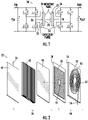
- Figure 1 schematically illustrates a wireless power transfer device 20 that is useful for a variety of situations.
- the wireless power transfer device 20 is used for high power transfer that involves high voltage.
- One example use for such a power transfer device is within an elevator system.
- the wireless power transfer device 20 includes a primary side (on the left in the drawing) that transfers power to a secondary side (on the right in the drawing).
- Each of the primary side and the secondary side include a LC series resonator 22 including an inductor panel 24 that establishes the inductive coupling between the primary and secondary side.
- a capacitor panel 26 is situated adjacent each inductor panel 24.
- FIG. 2 is an exploded view schematically illustrating an example configuration of a LC series resonator 22.
- the inductor panel in this example includes a conductive coil 30 arranged in a single layer.
- the conductive coil 30 is formed of a single conductor.
- the conductive coil 30 is at least partially secured to a coil support 32.
- the conductive coil 30 and the coil support 32 can be considered one layer of the example inductor panel 24.
- the coil support 32 comprises a resin material that is cast or molded onto or against a side of the coil 30.
- the inductor panel 24 includes a magnetic core 34 situated adjacent the conductive coil 30.
- a relatively thin electrically isolating layer 36 is situated between the magnetic core 34 and the coil 30.
- Another electrically isolating layer 38 is situated on an opposite side of the magnetic core 34.
- example inductor panel 24 includes a magnetic core, which is useful for high power wireless power transfer, some embodiments include an inductor panel without a magnetic core.
- the magnetic core 34 is arranged in a single layer.
- the example capacitor panel 26 of Figure 2 includes a first conductive plate 40 situated adjacent one side of the inductor panel 24.
- the first conductive plate 40 is received against the isolating layer 38 in this example.
- a dielectric layer 42 is situated adjacent the first conductive plate 40.
- a second conductive plate 44 is situated adjacent to the dielectric layer 42 on an opposite side of the dielectric layer 42 from the first conductive plate 40. The conductive plates 40 and 44 and the dielectric later 42 establish a capacitor.
- the first conductive plate 40 serves several functions in this example embodiment.
- the first conductive plate 40 is one plate of the capacitor.
- the first conductive plate adjacent the inductor panel 24 also acts as a shield for EMI by blocking stray or undesired electromagnetic radiation that is not needed or used for the wireless power transfer coupling.
- Another function of the example first conductive plate 40 is that the size, geometry and location of the plate 40 facilitates dissipating heat from the inductor panel 24.
- the conductive coil 30 includes one end 50 that is electrically coupled with the first conductive plate 40.
- the electrical connection is established at least partially through a window 52 through the magnetic core 34.
- An opposite end 54 of the conductive coil 30 is connected with another portion of the wireless power transfer device 20 as schematically shown in Figure 1 , for example.
- the capacitor panel 26 includes a lead 56 electrically coupling the capacitor with another portion of the wireless power transfer device 20.
- a LC series resonator configuration like that shown in the drawings integrates the inductive and capacitive capabilities of the LC series resonator 22 into a single package that provides a compact design.
- One feature of the example arrangement is that there is a reduced or minimized connection distance between the inductor and capacitor. Reducing this connection distance avoids shifting the resonant frequency of the LC series resonator 22. Additionally, the reduced connection distance contributes to reducing or minimizing the radiated EMI of the inductor panel 24.
- the illustrated example configuration is useful for high power conditions where voltages on the order of 400 volts and power on the order of 10 kilowatts can effectively be wirelessly transferred while dissipating heat and protecting against undesired EMI or noise all within a compact, integrated package.
- FIG. 3 schematically illustrates another configuration of a conductive coil 30 and a coil support layer 32.
- the conductive coil 30 in this example comprises a single conductor having two ends 50 and 54.
- the coil is arranged in a single layer and is at least partially embedded in the material of the coil support 32, which is a non-conductive resin in this example.
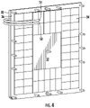
- Figure 4 illustrates an example arrangement of an electrically isolating layer 36 received against the coil support 32 between the conductive coil 30 and the magnetic core 34.
- the magnetic core 34 includes a plurality of ferrite plates that are arranged in a single layer including a window 52 through which the electrical connection between the conductive coil 30 and the first conductive plate 40 of the capacitor panel 26 will be made. Having that electrical coupling extend over the very small distance between the single layer of the conductive coil 30 and the first conductive plate 40 and keeping that electrical connection within the package of the LC series resonator 22 contributes to reducing any EMI or noise that would otherwise be associated with the connection between the inductor and the capacitor of the LC series resonator 22.
- the compact, integrated arrangement of an inductor panel 24 and capacitor panel 26 provides a LC series resonator that is useful for a variety of wireless power transfer devices including those that are intended for high power, high voltage conditions.
- the way in which the various layers of the panels are arranged renders the LC series resonator better than typical circuitry in several respects.
- the compact arrangement includes using at least one of the plates of the capacitor as an electromagnetic shield. The material and geometry of the plate also dissipates heat.
Landscapes
- Engineering & Computer Science (AREA)
- Power Engineering (AREA)
- Computer Networks & Wireless Communication (AREA)
- Microelectronics & Electronic Packaging (AREA)
- Physics & Mathematics (AREA)
- Electromagnetism (AREA)
- Signal Processing (AREA)
- Manufacturing & Machinery (AREA)
- Electric Propulsion And Braking For Vehicles (AREA)
- Regulation Of General Use Transformers (AREA)
- Coils Or Transformers For Communication (AREA)
Abstract
Description
- Wireless power transfer devices typically rely on an inductive linkage between two inductors to transfer energy from a primary side to a secondary side. Devices having a resonant topology typically include a capacitor associated with each inductor. The inductor and capacitor form a LC series resonator. While such arrangements have proven useful, they present various challenges.
- For example, high power wireless transfer that involves high voltage usually requires some accommodation for dissipating heat. Electromagnet shielding is also usually required to reduce electromagnetic noise or interference associated with the radiated energy of the magnetic field of the primary or transmitter coil. The electromagnetic field of the primary coil is desired for a wireless coupling with the secondary coil but radiation not involved in the coupling that causes electromagnetic interference (EMI) with other devices or components is undesired. The way in which the capacitor and inductor are arranged in typical resonant wireless power transfer topologies tends to increase the amount of EMI rather than reduce it.
- An illustrative example embodiment of a wireless power transfer device includes an inductor panel and a capacitor panel adjacent the inductor panel. The capacitor panel includes a first conductive plate adjacent one side of the inductor panel, a dielectric layer adjacent the first conductive plate, and a second conductive plate adjacent the dielectric layer on an opposite of the dielectric layer from the first conductive plate.
- In addition to one or more of the features described above, or as an alternative, the inductor panel includes a conductive coil and a magnetic core adjacent the conductive coil.
- In addition to one or more of the features described above, or as an alternative, the conductive coil comprises at least one conductor arranged in a single layer and the magnetic core is arranged in a single layer.
- In addition to one or more of the features described above, or as an alternative, the conductive coil comprises a single conductor having two ends and the magnetic core comprises a plurality of core segments.
- In addition to one or more of the features described above, or as an alternative, the magnetic core includes a window through the magnetic core, the wireless power transfer device includes an electrically conductive connection between the first conductive plate and one end of the single conductor, and the electrically conductive connection is situated at least partially within the window.
- In addition to one or more of the features described above, or as an alternative, an electrically isolating layer is included between the magnetic core and the conductive coil.
- In addition to one or more of the features described above, or as an alternative, the inductor panel includes a coiled conductor arranged in a first layer and a magnetic core arranged in a second layer adjacent the first layer and the inductor panel includes a coil support at least partially surrounding the coiled conductor.
- In addition to one or more of the features described above, or as an alternative, the coil support comprises a resin material.
- In addition to one or more of the features described above, or as an alternative, the first conductive plate is configured as an electromagnetic shield that reduces radiation of a magnetic field of the inductor panel.
- In addition to one or more of the features described above, or as an alternative, the inductor panel and the capacitor panel define a package and an electrically conductive connection is between the inductor panel and the first conductive plate within the package.
- In addition to one or more of the features described above, or as an alternative, the inductor panel and the capacitor panel establish a first LC series resonator and a second LC series resonator includes another inductor panel and another capacitor panel.
- An illustrative example embodiment of a method of making a wireless power transfer device includes forming an inductor panel and situating a capacitor panel adjacent the inductor panel. The capacitor panel includes a first conductive plate adjacent one side of the inductor panel, a dielectric layer adjacent the first conductive plate, and a second conductive plate adjacent the dielectric layer on an opposite of the dielectric layer from the first conductive plate.
- In addition to one or more of the features described above, or as an alternative, forming the inductor panel comprises arranging at least one conductor to form a conductive coil and situating a magnetic core adjacent the conductive coil.
- In addition to one or more of the features described above, or as an alternative, forming the inductor panel comprises arranging the conductive coil in a single layer and arranging the magnetic core in a single layer.
- In addition to one or more of the features described above, or as an alternative, the method includes establishing a window through the magnetic core and establishing an electrically conductive connection between the first conductive plate and one end of the single conductor at least partially within the window.
- In addition to one or more of the features described above, or as an alternative, forming the inductor panel comprises arranging a coiled conductor in a first layer, arranging a magnetic core in a second layer adjacent the first layer, and at least partially surrounding the coiled conductor by a coil support.
- In addition to one or more of the features described above, or as an alternative, the method includes forming the coil support of a resin material.
- In addition to one or more of the features described above, or as an alternative, the method includes placing an electrically isolating layer between the inductor panel and the first conductive plate.
- In addition to one or more of the features described above, or as an alternative, the method includes configuring the first conductive plate as an electromagnetic shield that reduces radiation of a magnetic field of the inductor panel.
- In addition to one or more of the features described above, or as an alternative, the method includes assembling the inductor panel and the capacitor panel as a package and including an electrically conductive connection between the inductor panel and the first conductive plate within the package.
- The various features and advantages of at least one disclosed example embodiment will become apparent to those skilled in the art from the following detailed description. The drawings that accompany the detailed description can be briefly described as follows.
-
-
Figure 1 schematically illustrates a wireless power transfer device. -
Figure 2 is an exploded view schematically illustrating selected features of a LC series resonator configuration of the embodiment ofFigure 1 . -
Figure 3 schematically illustrates an inductor coil configuration according to an example embodiment. -
Figure 4 schematically illustrates a magnetic core configuration adjacent the inductor coil ofFigure 3 . - Wireless power transfer devices including features like those of the example embodiments described below have a unique LC series resonator configuration. A compact, integrated package provides the wireless coupling operation of a LC series resonator while reducing or minimizing electromagnetic noise and dissipating heat.
-
Figure 1 schematically illustrates a wirelesspower transfer device 20 that is useful for a variety of situations. In some embodiments, the wirelesspower transfer device 20 is used for high power transfer that involves high voltage. One example use for such a power transfer device is within an elevator system. - The wireless
power transfer device 20 includes a primary side (on the left in the drawing) that transfers power to a secondary side (on the right in the drawing). Each of the primary side and the secondary side include aLC series resonator 22 including aninductor panel 24 that establishes the inductive coupling between the primary and secondary side. Acapacitor panel 26 is situated adjacent eachinductor panel 24. -
Figure 2 is an exploded view schematically illustrating an example configuration of aLC series resonator 22. The inductor panel in this example includes aconductive coil 30 arranged in a single layer. In this example embodiment, theconductive coil 30 is formed of a single conductor. Theconductive coil 30 is at least partially secured to acoil support 32. Theconductive coil 30 and thecoil support 32 can be considered one layer of theexample inductor panel 24. In some example embodiments, thecoil support 32 comprises a resin material that is cast or molded onto or against a side of thecoil 30. - The
inductor panel 24 includes amagnetic core 34 situated adjacent theconductive coil 30. A relatively thin electrically isolatinglayer 36 is situated between themagnetic core 34 and thecoil 30. Another electrically isolatinglayer 38 is situated on an opposite side of themagnetic core 34. - While the
example inductor panel 24 includes a magnetic core, which is useful for high power wireless power transfer, some embodiments include an inductor panel without a magnetic core. Themagnetic core 34 is arranged in a single layer. - The
example capacitor panel 26 ofFigure 2 includes a firstconductive plate 40 situated adjacent one side of theinductor panel 24. The firstconductive plate 40 is received against theisolating layer 38 in this example. Adielectric layer 42 is situated adjacent the firstconductive plate 40. A secondconductive plate 44 is situated adjacent to thedielectric layer 42 on an opposite side of thedielectric layer 42 from the firstconductive plate 40. Theconductive plates - The first
conductive plate 40 serves several functions in this example embodiment. The firstconductive plate 40 is one plate of the capacitor. The first conductive plate adjacent theinductor panel 24 also acts as a shield for EMI by blocking stray or undesired electromagnetic radiation that is not needed or used for the wireless power transfer coupling. Another function of the example firstconductive plate 40 is that the size, geometry and location of theplate 40 facilitates dissipating heat from theinductor panel 24. - The
conductive coil 30 includes oneend 50 that is electrically coupled with the firstconductive plate 40. The electrical connection is established at least partially through awindow 52 through themagnetic core 34. Anopposite end 54 of theconductive coil 30 is connected with another portion of the wirelesspower transfer device 20 as schematically shown inFigure 1 , for example. Thecapacitor panel 26 includes a lead 56 electrically coupling the capacitor with another portion of the wirelesspower transfer device 20. - A LC series resonator configuration like that shown in the drawings integrates the inductive and capacitive capabilities of the
LC series resonator 22 into a single package that provides a compact design. One feature of the example arrangement is that there is a reduced or minimized connection distance between the inductor and capacitor. Reducing this connection distance avoids shifting the resonant frequency of theLC series resonator 22. Additionally, the reduced connection distance contributes to reducing or minimizing the radiated EMI of theinductor panel 24. - The illustrated example configuration is useful for high power conditions where voltages on the order of 400 volts and power on the order of 10 kilowatts can effectively be wirelessly transferred while dissipating heat and protecting against undesired EMI or noise all within a compact, integrated package.
-
Figure 3 schematically illustrates another configuration of aconductive coil 30 and acoil support layer 32. Theconductive coil 30 in this example comprises a single conductor having two ends 50 and 54. The coil is arranged in a single layer and is at least partially embedded in the material of thecoil support 32, which is a non-conductive resin in this example. -
Figure 4 illustrates an example arrangement of an electrically isolatinglayer 36 received against thecoil support 32 between theconductive coil 30 and themagnetic core 34. In this example, themagnetic core 34 includes a plurality of ferrite plates that are arranged in a single layer including awindow 52 through which the electrical connection between theconductive coil 30 and the firstconductive plate 40 of thecapacitor panel 26 will be made. Having that electrical coupling extend over the very small distance between the single layer of theconductive coil 30 and the firstconductive plate 40 and keeping that electrical connection within the package of theLC series resonator 22 contributes to reducing any EMI or noise that would otherwise be associated with the connection between the inductor and the capacitor of theLC series resonator 22. - The compact, integrated arrangement of an
inductor panel 24 andcapacitor panel 26 provides a LC series resonator that is useful for a variety of wireless power transfer devices including those that are intended for high power, high voltage conditions. The way in which the various layers of the panels are arranged renders the LC series resonator better than typical circuitry in several respects. The compact arrangement includes using at least one of the plates of the capacitor as an electromagnetic shield. The material and geometry of the plate also dissipates heat. - The preceding description is exemplary rather than limiting in nature. Variations and modifications to the disclosed examples may become apparent to those skilled in the art that do not necessarily depart from the essence of this invention. The scope of legal protection given to this invention can only be determined by studying the following claims.
Claims (15)
- A wireless power transfer device, comprising:an inductor panel; anda capacitor panel adjacent the inductor panel, the capacitor panel includinga first conductive plate adjacent one side of the inductor panel,a dielectric layer adjacent the first conductive plate, anda second conductive plate adjacent the dielectric layer on an opposite of the dielectric layer from the first conductive plate.
- The wireless power transfer device of claim 1, wherein the inductor panel includes a conductive coil and a magnetic core adjacent the conductive coil.
- The wireless power transfer device of claim 2, whereinthe conductive coil comprises at least one conductor arranged in a single layer, andthe magnetic core is arranged in a single layer.
- The wireless power transfer device of claim 3, whereinthe conductive coil comprises a single conductor having two ends, andthe magnetic core comprises a plurality of core segments.
- The wireless power transfer device of claim 4, whereinthe magnetic core includes a window through the magnetic core,the wireless power transfer device includes an electrically conductive connection between the first conductive plate and one end of the single conductor, andthe electrically conductive connection is situated at least partially within the window.
- The wireless power transfer device of any of claims 2 and 5, including an electrically isolating layer between the magnetic core and the conductive coil.
- The wireless power transfer device of any preceding claim, whereinthe inductor panel includes a coiled conductor arranged in a first layer and a magnetic core arranged in a second layer adjacent the first layer, andthe inductor panel includes a coil support at least partially surrounding the coiled conductor.
- The wireless power transfer device of claim 7, wherein the coil support comprises a resin material.
- The wireless power transfer device of any preceding claim, wherein the first conductive plate is configured as an electromagnetic shield that reduces radiation of a magnetic field of the inductor panel.
- The wireless power transfer device of any preceding claim, wherein the inductor panel and the capacitor panel define a package and comprising an electrically conductive connection between the inductor panel and the first conductive plate within the package.
- The wireless power transfer device of any preceding claim, wherein the inductor panel and the capacitor panel establish a first LC series resonator and comprising a second LC series resonator including another inductor panel and another capacitor panel.
- A method of making a wireless power transfer device, the method comprising:forming an inductor panel; andsituating a capacitor panel adjacent the inductor panel, the capacitor panel includinga first conductive plate adjacent one side of the inductor panel,a dielectric layer adjacent the first conductive plate, anda second conductive plate adjacent the dielectric layer on an opposite of the dielectric layer from the first conductive plate.
- The method of claim 12, wherein forming the inductor panel comprisesarranging at least one conductor to form a conductive coil andsituating a magnetic core adjacent the conductive coil.
- The method of claim 13, wherein forming the inductor panel comprisesarranging the conductive coil in a single layer andarranging the magnetic core in a single layer.
- The method of any of claims 12 to 14, including placing an electrically isolating layer between the inductor panel and the first conductive plate.
Applications Claiming Priority (1)
| Application Number | Priority Date | Filing Date | Title |
|---|---|---|---|
| US17/122,133 US11876384B2 (en) | 2020-12-15 | 2020-12-15 | Wireless power transfer device |
Publications (1)
| Publication Number | Publication Date |
|---|---|
| EP4016564A1 true EP4016564A1 (en) | 2022-06-22 |
Family
ID=78598904
Family Applications (1)
| Application Number | Title | Priority Date | Filing Date |
|---|---|---|---|
| EP21207698.8A Withdrawn EP4016564A1 (en) | 2020-12-15 | 2021-11-11 | Wireless power transfer device |
Country Status (4)
| Country | Link |
|---|---|
| US (1) | US11876384B2 (en) |
| EP (1) | EP4016564A1 (en) |
| KR (1) | KR20220085712A (en) |
| CN (1) | CN114640189A (en) |
Cited By (2)
| Publication number | Priority date | Publication date | Assignee | Title |
|---|---|---|---|---|
| WO2024170278A1 (en) * | 2023-02-14 | 2024-08-22 | Siemens Aktiengesellschaft | Device for inductively charging a battery of a motor vehicle |
| EP4697369A1 (en) * | 2024-08-12 | 2026-02-18 | Siemens Aktiengesellschaft | Electromagnetic arrangement, transformer arrangement, choke arrangement and charging converter |
Families Citing this family (1)
| Publication number | Priority date | Publication date | Assignee | Title |
|---|---|---|---|---|
| US12606035B2 (en) * | 2022-12-06 | 2026-04-21 | Volkswagen Aktiengesellschaft | Devices, systems, and methods for wireless vehicle charging |
Citations (3)
| Publication number | Priority date | Publication date | Assignee | Title |
|---|---|---|---|---|
| DE102012202472A1 (en) * | 2012-02-17 | 2013-08-22 | Siemens Aktiengesellschaft | Device for contactless transmission of energy to a corresponding device |
| JP2019126202A (en) * | 2018-01-17 | 2019-07-25 | Tdk株式会社 | Lc circuit unit, wireless transmission equipment, wireless power reception device, and wireless power transmission system |
| US20200152376A1 (en) * | 2018-11-12 | 2020-05-14 | Toyota Jidosha Kabushiki Kaisha | Coil unit |
Family Cites Families (19)
| Publication number | Priority date | Publication date | Assignee | Title |
|---|---|---|---|---|
| DE19751017C2 (en) * | 1997-11-18 | 2002-04-11 | Siemens Ag | MR imaging system with galvanically isolated coil element |
| US7136028B2 (en) * | 2004-08-27 | 2006-11-14 | Freescale Semiconductor, Inc. | Applications of a high impedance surface |
| US7136029B2 (en) * | 2004-08-27 | 2006-11-14 | Freescale Semiconductor, Inc. | Frequency selective high impedance surface |
| US7423608B2 (en) * | 2005-12-20 | 2008-09-09 | Motorola, Inc. | High impedance electromagnetic surface and method |
| ES2371787T5 (en) * | 2008-06-12 | 2016-02-19 | Abb Technology Ag | Test set for an alternating current test of high voltage electrical components |
| US9025798B2 (en) * | 2010-06-09 | 2015-05-05 | Stephen Saint Vincent | Multi-coaxial transducers and methods |
| CN102456936A (en) * | 2010-10-26 | 2012-05-16 | 新科实业有限公司 | Wireless charging system, battery and electronic device with wireless charging function |
| EP3425651A3 (en) * | 2011-06-14 | 2019-01-16 | Panasonic Corporation | Communication apparatus |
| JP5790200B2 (en) * | 2011-06-27 | 2015-10-07 | ソニー株式会社 | Communication apparatus and communication system |
| JP6071654B2 (en) * | 2013-03-06 | 2017-02-01 | 株式会社東芝 | Coil, power receiving device, and power transmitting device |
| US9570222B2 (en) * | 2013-05-28 | 2017-02-14 | Tdk Corporation | Vector inductor having multiple mutually coupled metalization layers providing high quality factor |
| CN105393465A (en) * | 2013-07-26 | 2016-03-09 | 皇家飞利浦有限公司 | Picking-up signals in electrically contactless manners |
| KR20150065428A (en) * | 2013-12-05 | 2015-06-15 | 엘지이노텍 주식회사 | Apparatus for transmitting wireless power |
| US20160111889A1 (en) * | 2014-10-20 | 2016-04-21 | Qualcomm Incorporated | Segmented conductive back cover for wireless power transfer |
| MX375816B (en) * | 2016-05-18 | 2025-03-07 | Nissan Motor | COIL UNIT. |
| CN106451701A (en) * | 2016-11-03 | 2017-02-22 | 深圳市同洁科技有限公司 | Wireless charging circuit and device |
| KR102031615B1 (en) * | 2017-03-28 | 2019-10-15 | 티디케이가부시기가이샤 | Soft magnetic ribbon for magnetic core, magnetic core, coil unit, and wireless power transmission unit |
| US10896780B2 (en) * | 2018-03-02 | 2021-01-19 | Intel IP Corporation | Resonant LC tank package and method of manufacture |
| WO2019224192A1 (en) * | 2018-05-22 | 2019-11-28 | Premo, Sa | Inductive energy emitter/receiver for an inductive charger of an electric vehicle |
-
2020
- 2020-12-15 US US17/122,133 patent/US11876384B2/en active Active
-
2021
- 2021-08-19 CN CN202110953105.9A patent/CN114640189A/en active Pending
- 2021-11-11 EP EP21207698.8A patent/EP4016564A1/en not_active Withdrawn
- 2021-11-24 KR KR1020210162977A patent/KR20220085712A/en active Pending
Patent Citations (3)
| Publication number | Priority date | Publication date | Assignee | Title |
|---|---|---|---|---|
| DE102012202472A1 (en) * | 2012-02-17 | 2013-08-22 | Siemens Aktiengesellschaft | Device for contactless transmission of energy to a corresponding device |
| JP2019126202A (en) * | 2018-01-17 | 2019-07-25 | Tdk株式会社 | Lc circuit unit, wireless transmission equipment, wireless power reception device, and wireless power transmission system |
| US20200152376A1 (en) * | 2018-11-12 | 2020-05-14 | Toyota Jidosha Kabushiki Kaisha | Coil unit |
Cited By (2)
| Publication number | Priority date | Publication date | Assignee | Title |
|---|---|---|---|---|
| WO2024170278A1 (en) * | 2023-02-14 | 2024-08-22 | Siemens Aktiengesellschaft | Device for inductively charging a battery of a motor vehicle |
| EP4697369A1 (en) * | 2024-08-12 | 2026-02-18 | Siemens Aktiengesellschaft | Electromagnetic arrangement, transformer arrangement, choke arrangement and charging converter |
Also Published As
| Publication number | Publication date |
|---|---|
| CN114640189A (en) | 2022-06-17 |
| KR20220085712A (en) | 2022-06-22 |
| US20220190645A1 (en) | 2022-06-16 |
| US11876384B2 (en) | 2024-01-16 |
Similar Documents
| Publication | Publication Date | Title |
|---|---|---|
| US20250239893A1 (en) | Wireless power transfer transmitter, system and method of wirelessly transferring power | |
| US11876384B2 (en) | Wireless power transfer device | |
| CN105529157B (en) | Compact embedded isolated transformer device and the method for manufacturing the device | |
| US6449178B1 (en) | Magnetron drive step-up transformer and transformer of magnetron drive power supply | |
| CN110620408B (en) | Wireless charger with electromagnetic shielding function | |
| US10117334B2 (en) | Magnetic assembly | |
| CN112586094B (en) | Circuit device and power conversion device | |
| US9941047B2 (en) | Shield for toroidal core electromagnetic device, and toroidal core electromagnetic devices utilizing such shields | |
| CN102077307A (en) | Transformer, power converter using the transformer, lighting device, lamp for vehicle, and vehicle | |
| CN105529159A (en) | Embedded magnetic component transformer device | |
| CN105529158A (en) | Embedded magnetic component transformer device | |
| US20210193381A1 (en) | Series self-resonant coil structure for conducting wireless power transfer | |
| US11303153B2 (en) | Wireless charging pad and wireless charging apparatus | |
| US20170324281A1 (en) | Wireless power trnsfer device | |
| WO2012005603A1 (en) | An icpt system, components and design method | |
| JP6324362B2 (en) | Wireless transmission equipment | |
| EP3319207B1 (en) | Wireless power transmission device for transmitting power using magnetic field and electric field, and wireless power receiving device for receiving power from the wireless power transmission device | |
| CN112688439A (en) | Wireless power transmission device | |
| US9520793B2 (en) | Stacked power converter assembly | |
| JP6774894B2 (en) | Electromagnetic field resonance type coupler | |
| EP1080614A1 (en) | Apparatus for coupling power into a body of gas | |
| KR20090023862A (en) | Insertion Stacking Inductor |
Legal Events
| Date | Code | Title | Description |
|---|---|---|---|
| PUAI | Public reference made under article 153(3) epc to a published international application that has entered the european phase |
Free format text: ORIGINAL CODE: 0009012 |
|
| STAA | Information on the status of an ep patent application or granted ep patent |
Free format text: STATUS: THE APPLICATION HAS BEEN PUBLISHED |
|
| AK | Designated contracting states |
Kind code of ref document: A1 Designated state(s): AL AT BE BG CH CY CZ DE DK EE ES FI FR GB GR HR HU IE IS IT LI LT LU LV MC MK MT NL NO PL PT RO RS SE SI SK SM TR |
|
| STAA | Information on the status of an ep patent application or granted ep patent |
Free format text: STATUS: REQUEST FOR EXAMINATION WAS MADE |
|
| 17P | Request for examination filed |
Effective date: 20221221 |
|
| RBV | Designated contracting states (corrected) |
Designated state(s): AL AT BE BG CH CY CZ DE DK EE ES FI FR GB GR HR HU IE IS IT LI LT LU LV MC MK MT NL NO PL PT RO RS SE SI SK SM TR |
|
| GRAP | Despatch of communication of intention to grant a patent |
Free format text: ORIGINAL CODE: EPIDOSNIGR1 |
|
| STAA | Information on the status of an ep patent application or granted ep patent |
Free format text: STATUS: GRANT OF PATENT IS INTENDED |
|
| RIC1 | Information provided on ipc code assigned before grant |
Ipc: H01F 27/36 20060101ALI20241210BHEP Ipc: H02J 50/12 20160101ALI20241210BHEP Ipc: H01F 38/14 20060101AFI20241210BHEP |
|
| INTG | Intention to grant announced |
Effective date: 20250113 |
|
| STAA | Information on the status of an ep patent application or granted ep patent |
Free format text: STATUS: THE APPLICATION IS DEEMED TO BE WITHDRAWN |
|
| 18D | Application deemed to be withdrawn |
Effective date: 20250514 |