EP4016151A1 - Faraday rotator interconnect as a through-via configuration in a patch architecture - Google Patents
Faraday rotator interconnect as a through-via configuration in a patch architecture Download PDFInfo
- Publication number
- EP4016151A1 EP4016151A1 EP21198382.0A EP21198382A EP4016151A1 EP 4016151 A1 EP4016151 A1 EP 4016151A1 EP 21198382 A EP21198382 A EP 21198382A EP 4016151 A1 EP4016151 A1 EP 4016151A1
- Authority
- EP
- European Patent Office
- Prior art keywords
- patch
- polarizer
- photonics
- faraday rotator
- die
- Prior art date
- Legal status (The legal status is an assumption and is not a legal conclusion. Google has not performed a legal analysis and makes no representation as to the accuracy of the status listed.)
- Granted
Links
Images





Classifications
-
- G—PHYSICS
- G02—OPTICS
- G02B—OPTICAL ELEMENTS, SYSTEMS OR APPARATUS
- G02B6/00—Light guides; Structural details of arrangements comprising light guides and other optical elements, e.g. couplings
- G02B6/24—Coupling light guides
- G02B6/42—Coupling light guides with opto-electronic elements
- G02B6/4201—Packages, e.g. shape, construction, internal or external details
- G02B6/4204—Packages, e.g. shape, construction, internal or external details the coupling comprising intermediate optical elements, e.g. lenses, holograms
- G02B6/4213—Packages, e.g. shape, construction, internal or external details the coupling comprising intermediate optical elements, e.g. lenses, holograms the intermediate optical elements being polarisation selective optical elements
-
- G—PHYSICS
- G02—OPTICS
- G02B—OPTICAL ELEMENTS, SYSTEMS OR APPARATUS
- G02B6/00—Light guides; Structural details of arrangements comprising light guides and other optical elements, e.g. couplings
- G02B6/24—Coupling light guides
- G02B6/42—Coupling light guides with opto-electronic elements
- G02B6/4201—Packages, e.g. shape, construction, internal or external details
- G02B6/4204—Packages, e.g. shape, construction, internal or external details the coupling comprising intermediate optical elements, e.g. lenses, holograms
- G02B6/4207—Packages, e.g. shape, construction, internal or external details the coupling comprising intermediate optical elements, e.g. lenses, holograms with optical elements reducing the sensitivity to optical feedback
- G02B6/4208—Packages, e.g. shape, construction, internal or external details the coupling comprising intermediate optical elements, e.g. lenses, holograms with optical elements reducing the sensitivity to optical feedback using non-reciprocal elements or birefringent plates, i.e. quasi-isolators
-
- G—PHYSICS
- G02—OPTICS
- G02B—OPTICAL ELEMENTS, SYSTEMS OR APPARATUS
- G02B6/00—Light guides; Structural details of arrangements comprising light guides and other optical elements, e.g. couplings
- G02B6/24—Coupling light guides
- G02B6/26—Optical coupling means
- G02B6/27—Optical coupling means with polarisation selective and adjusting means
- G02B6/2746—Optical coupling means with polarisation selective and adjusting means comprising non-reciprocal devices, e.g. isolators, FRM, circulators, quasi-isolators
-
- G—PHYSICS
- G02—OPTICS
- G02B—OPTICAL ELEMENTS, SYSTEMS OR APPARATUS
- G02B6/00—Light guides; Structural details of arrangements comprising light guides and other optical elements, e.g. couplings
- G02B6/24—Coupling light guides
- G02B6/42—Coupling light guides with opto-electronic elements
- G02B6/4201—Packages, e.g. shape, construction, internal or external details
- G02B6/4256—Details of housings
- G02B6/4257—Details of housings having a supporting carrier or a mounting substrate or a mounting plate
-
- G—PHYSICS
- G02—OPTICS
- G02B—OPTICAL ELEMENTS, SYSTEMS OR APPARATUS
- G02B6/00—Light guides; Structural details of arrangements comprising light guides and other optical elements, e.g. couplings
- G02B6/24—Coupling light guides
- G02B6/42—Coupling light guides with opto-electronic elements
- G02B6/4201—Packages, e.g. shape, construction, internal or external details
- G02B6/4274—Electrical aspects
- G02B6/428—Electrical aspects containing printed circuit boards [PCB]
-
- G—PHYSICS
- G02—OPTICS
- G02F—OPTICAL DEVICES OR ARRANGEMENTS FOR THE CONTROL OF LIGHT BY MODIFICATION OF THE OPTICAL PROPERTIES OF THE MEDIA OF THE ELEMENTS INVOLVED THEREIN; NON-LINEAR OPTICS; FREQUENCY-CHANGING OF LIGHT; OPTICAL LOGIC ELEMENTS; OPTICAL ANALOGUE/DIGITAL CONVERTERS
- G02F1/00—Devices or arrangements for the control of the intensity, colour, phase, polarisation or direction of light arriving from an independent light source, e.g. switching, gating or modulating; Non-linear optics
- G02F1/01—Devices or arrangements for the control of the intensity, colour, phase, polarisation or direction of light arriving from an independent light source, e.g. switching, gating or modulating; Non-linear optics for the control of the intensity, phase, polarisation or colour
- G02F1/0136—Devices or arrangements for the control of the intensity, colour, phase, polarisation or direction of light arriving from an independent light source, e.g. switching, gating or modulating; Non-linear optics for the control of the intensity, phase, polarisation or colour for the control of polarisation, e.g. state of polarisation [SOP] control, polarisation scrambling, TE-TM mode conversion or separation
-
- G—PHYSICS
- G02—OPTICS
- G02F—OPTICAL DEVICES OR ARRANGEMENTS FOR THE CONTROL OF LIGHT BY MODIFICATION OF THE OPTICAL PROPERTIES OF THE MEDIA OF THE ELEMENTS INVOLVED THEREIN; NON-LINEAR OPTICS; FREQUENCY-CHANGING OF LIGHT; OPTICAL LOGIC ELEMENTS; OPTICAL ANALOGUE/DIGITAL CONVERTERS
- G02F1/00—Devices or arrangements for the control of the intensity, colour, phase, polarisation or direction of light arriving from an independent light source, e.g. switching, gating or modulating; Non-linear optics
- G02F1/01—Devices or arrangements for the control of the intensity, colour, phase, polarisation or direction of light arriving from an independent light source, e.g. switching, gating or modulating; Non-linear optics for the control of the intensity, phase, polarisation or colour
- G02F1/09—Devices or arrangements for the control of the intensity, colour, phase, polarisation or direction of light arriving from an independent light source, e.g. switching, gating or modulating; Non-linear optics for the control of the intensity, phase, polarisation or colour based on magneto-optical elements, e.g. exhibiting Faraday effect
-
- H—ELECTRICITY
- H10—SEMICONDUCTOR DEVICES; ELECTRIC SOLID-STATE DEVICES NOT OTHERWISE PROVIDED FOR
- H10W—GENERIC PACKAGES, INTERCONNECTIONS, CONNECTORS OR OTHER CONSTRUCTIONAL DETAILS OF DEVICES COVERED BY CLASS H10
- H10W70/00—Package substrates; Interposers; Redistribution layers [RDL]
- H10W70/60—Insulating or insulated package substrates; Interposers; Redistribution layers
- H10W70/62—Insulating or insulated package substrates; Interposers; Redistribution layers characterised by their interconnections
- H10W70/63—Vias, e.g. via plugs
- H10W70/635—Through-vias
-
- H—ELECTRICITY
- H10—SEMICONDUCTOR DEVICES; ELECTRIC SOLID-STATE DEVICES NOT OTHERWISE PROVIDED FOR
- H10W—GENERIC PACKAGES, INTERCONNECTIONS, CONNECTORS OR OTHER CONSTRUCTIONAL DETAILS OF DEVICES COVERED BY CLASS H10
- H10W90/00—Package configurations
-
- H—ELECTRICITY
- H10—SEMICONDUCTOR DEVICES; ELECTRIC SOLID-STATE DEVICES NOT OTHERWISE PROVIDED FOR
- H10W—GENERIC PACKAGES, INTERCONNECTIONS, CONNECTORS OR OTHER CONSTRUCTIONAL DETAILS OF DEVICES COVERED BY CLASS H10
- H10W90/00—Package configurations
- H10W90/701—Package configurations characterised by the relative positions of pads or connectors relative to package parts
-
- G—PHYSICS
- G02—OPTICS
- G02B—OPTICAL ELEMENTS, SYSTEMS OR APPARATUS
- G02B6/00—Light guides; Structural details of arrangements comprising light guides and other optical elements, e.g. couplings
- G02B6/24—Coupling light guides
- G02B6/42—Coupling light guides with opto-electronic elements
- G02B6/4201—Packages, e.g. shape, construction, internal or external details
- G02B6/4266—Thermal aspects, temperature control or temperature monitoring
- G02B6/4268—Cooling
-
- H—ELECTRICITY
- H10—SEMICONDUCTOR DEVICES; ELECTRIC SOLID-STATE DEVICES NOT OTHERWISE PROVIDED FOR
- H10W—GENERIC PACKAGES, INTERCONNECTIONS, CONNECTORS OR OTHER CONSTRUCTIONAL DETAILS OF DEVICES COVERED BY CLASS H10
- H10W70/00—Package substrates; Interposers; Redistribution layers [RDL]
- H10W70/60—Insulating or insulated package substrates; Interposers; Redistribution layers
- H10W70/62—Insulating or insulated package substrates; Interposers; Redistribution layers characterised by their interconnections
- H10W70/65—Shapes or dispositions of interconnections
Definitions
- Embodiments of the present disclosure relate to electronic packages, and more particularly to photonics packages with a Faraday rotator between an optical cable and the photonics die.
- the microelectronic industry has begun using optical connections as a way to increase bandwidth and performance.
- an optical fiber is coupled to a photonics die.
- the current coupling architectures include direct coupling between the interfaces. Such direct coupling does not fundamentally improve signal-to-noise ratios. In fact, these direct light coupling architectures may result in reflected light at the interface. The reflected light generates optical interference. The optical interference decreases the signal-to-noise ratio and can even result in inaccurate signals being propagated to the receivers.
- Described herein are photonics packages with a Faraday rotator between an optical cable and the photonics die, in accordance with various embodiments.
- various aspects of the illustrative implementations will be described using terms commonly employed by those skilled in the art to convey the substance of their work to others skilled in the art.
- the present invention may be practiced with only some of the described aspects.
- specific numbers, materials and configurations are set forth in order to provide a thorough understanding of the illustrative implementations.
- the present invention may be practiced without the specific details.
- well-known features are omitted or simplified in order not to obscure the illustrative implementations.
- embodiments disclosed herein include the integration of Faraday rotators into the photonics package architectures.
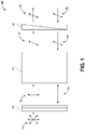
- An example schematic of the functioning of a Faraday rotator 160 is shown in Figure 1 .
- the Faraday rotator 160 comprises a first polarizer 165, a magnetic region 166, and a second polarizer 167 on the opposite side of the magnetic region 166 from the first polarizer 165.
- Incoming light 161 may have random polarization.
- the light 162 may be vertically polarized.
- the light 162 propagates through the magnetic region 166 where the magnetic field results in the polarization being shifted, as shown in light 163.
- a 45° polarization shift may be provided in some embodiments.
- Light 163 then passes through the second polarizer 167, which restricts light to only the selected polarization shift induced by the magnetic region 166, as shown by light 164.
- the angled polarized light 168 and 169 passes back through the magnetic region 166.
- the magnetic region 166 again shifts the polarization. For example, when a 45° polarization is used, the polarization of the light 169 is further shifted so that light 170 is 90° polarized. It is to be appreciated that such a Faraday architecture may result in the filtering out of reflections from the optical path. As such, the signal-to-noise ratio is increased, and performance of the optical interconnects are improved.
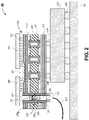
- the electronic system 200 comprises a patch on interposer (PoINT) architecture.
- the PoINT architecture may comprise a board 201.
- the board 201 may be a printed circuit board (PCB) or the like.
- an interposer 202 is attached to the board 201 by interconnects 203.
- the interconnects 203 are shown as being solder balls, but it is to be appreciated that any interconnect architecture may be used, such as sockets or the like.
- the interposer 202 may comprise conductive routing (not shown).
- the conductive routing within the interposer 202 may allow for conductive coupling between a top surface and a bottom surface of the interposer 202.
- the conductive routing may comprise pads, traces, vias, and the like.
- a patch 205 is attached to the interposer 202.
- the patch 205 may be coupled to the interposer 202 by interconnects 204, such as solder balls or the like.
- the patch 205 comprises a core 212 and conductive routing layers 213 above and below the core 212. Through core vias 211 may conductively couple the top routing layer 213 to the bottom routing layer 213.
- a coreless patch 205 may also be used.
- the patch 205 may comprise a compute die 220 and a photonics die 225.
- the compute die 220 may be any type of die, such as, but not limited to a processor, a graphics processor, a field-programmable gate array (FPGA), a system on a chip (SoC), a memory, or the like.
- the photonics die 225 comprises features for converting signals between the optical regime and the electrical regime.
- the photonics die 225 may comprise a laser and/or a photodiode.
- the compute die 220 is communicatively coupled to the photonics die 225 by a bridge 227 that is embedded in the top routing layer 213 of the patch 205.
- the bridge 227 provides a dimensionally stable substrate on which high density conductive routing can be provided.
- the patch 205 is arranged so that it overhangs an edge of the interposer 202.
- the patch 205 in Figure 2 overhangs the left edge of the interposer 202. Overhanging the interposer 202 allows for a bottom surface of the patch 205 to be exposed. Particularly, a space between the underlying board 201 and the bottom surface of the patch 205 is sufficient to provide an optical connection to the photonics die 225 from below.
- an optical cable 234 is connected to a connector 233.
- the connector 233 interfaces with a Faraday rotator 230 that passes through a thickness of the patch 205.
- the Faraday rotator 230 is positioned within a footprint of the photonics die 225. As such, an optical path is provided through the Faraday rotator 230 from the connector 233 to the photonics die 225.
- the Faraday rotator 230 comprises a housing 232.
- the housing 232 may be a tube.
- the housing 232 is mechanically coupled to the patch 205 by a dielectric layer 231.
- the dielectric layer 231 is a material that expands during a heat treatment. As such, the Faraday rotator 230 can be inserted into the patch 205, and the heat treatment secures the Faraday rotator 230 to the patch 205.
- the Faraday rotator 230 may comprise a first polarizer 236 and a second polarizer 237.
- the first polarizer 236 may be a vertical polarizer and the second polarizer 237 may be an angled polarizer (e.g., 45°). That is, the first polarizer 236 may be different than the second polarizer 237.
- a magnetic region is provided between the first polarizer 236 and the second polarizer 237.
- the magnetic region may comprise a permanent magnet 235.
- the permanent magnet 235 may be a shell that wraps around an optically clear layer 238.
- the permanent magnet 235 has a magnetic field that modifies the orientation of the incoming vertically polarized light. For example, the permanent magnet 235 may result in 45° polarized light in some embodiments.
- the efficiency of the Faraday rotator 230 may be further improved by including lenses.
- a first lens 239 A may be provided between the first polarizer 236 and the connector 233
- a second lens 239 B may be provided between the second polarizer 237 and the photonics die 225.
- FIG. 3A-3D a series of cross-sectional illustrations depicting a process for fabricating a patch 305 is shown, in accordance with an embodiment.
- the patch 305 in Figures 3A-3D may be substantially similar to the patch 205 in Figure 2 .
- the patch 305 may comprise a core 312 with routing layers 313 above and below the core 312. Through core vias 311 may electrically couple the top routing layers 313 to the bottom routing layers 313.
- the patch 305 may be coreless.
- conductive traces are shown in the routing layers 313.
- conductive vias, traces, and pads may be provided in the routing layers 313 in order to provide the necessary conductive routing.
- a bridge 327 for providing high density routing may also be provided in the top routing layers 313.
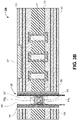
- a hole 341 is formed through the patch 305.
- the hole 341 may be formed with any drilling process.
- the hole 341 may be mechanically drilled or drilled with a laser.
- the sidewalls of the hole 341 may be tapered, as is common in laser drilled architectures.
- the hole 341 passes through the top routing layers 313, the core 312, and the bottom routing layers 313. That is, the hole 341 extends through an entire thickness of the patch 305.
- the Faraday rotator 330 comprise a housing 332 that is tubular.
- An outer surface of the housing 332 may be lined with a dielectric material 331.
- the outer diameter of the dielectric material 331 may be smaller than a diameter of the hole 341.
- the Faraday rotator 330 may comprise a first polarizer 336 and a second polarizer 337.
- the first polarizer 336 may be a vertical polarizer and the second polarizer 337 may be an angled polarizer (e.g., 45°). That is, the first polarizer 336 may be different than the second polarizer 337.
- a magnetic region is provided between the first polarizer 336 and the second polarizer 337.
- the magnetic region may comprise a permanent magnet 335.
- the permanent magnet 335 may be a shell that wraps around an optically clear layer 338. While shown as a physical layer in Figure 3B , it is to be appreciated that the permanent magnet 335 may have an air core in some embodiments.
- the permanent magnet 335 has a magnetic field that modifies the orientation of the incoming vertically polarized light. For example, the permanent magnet 335 may result in 45° polarized light in some embodiments.
- the permanent magnet 335 may be in direct contact with the first polarizer 336 and the second polarizer 337.
- a bottom surface of the permanent magnet 335 may be in direct contact with a top surface of the first polarizer 336, and a top surface of the permanent magnet 335 may be in direct contact with a bottom surface of the second polarizer 337.
- the permanent magnet 335 may have an outer diameter that is substantially equal to diameters of the first polarizer 336 and the second polarizer 337.
- the Faraday rotator 330 may also comprise a first lens 339 A and a second lens 339 B .
- the first lens 339 A is within the housing below the first polarizer 336
- the second lens 339 B is within the housing above the second polarizer 337.
- the lenses 339 A and 339 B allow for improved efficiency by focusing the light passing through the Faraday rotator 330.
- the first polarizer 336, the second polarizer 337, and the permanent magnet 335 are positioned at approximately a midpoint of the housing 332. That is, the first polarizer 336, the second polarizer 337, and the permanent magnet 335 are positioned substantially within the core 312 of the patch 305. However, it is to be appreciated that the first polarizer 336, the second polarizer 337, and the permanent magnet 335 may be positioned at any vertical location within the patch 305. Additionally, while shown as be directly in contact with each other, embodiments may include spacings between one or more of the first polarizer 336, the second polarizer 337, and the permanent magnet 335.
- the thermal treatment may be at an elevated temperature (e.g., 300°C or more) for a designated period of time.
- the heat treatment induces a physical change in the dielectric material 331.
- an outer diameter of the dielectric material 331 is increased by the heat treatment.
- the outer diameter of the dielectric material 331 may expand to completely fill the hole 341.
- the dielectric material 331 mechanically couples the Faraday rotator 330 to the patch 305.
- the compute die 320 and the photonics die 325 may be attached to the patch by interconnects 321. While shown as solder balls, it is to be appreciated that the interconnects 321 may be any first level interconnect (FLI).
- the photonics die 325 may be communicatively coupled to the compute die 320 by the bridge 327 in the top routing layers 313.
- the photonics die 325 extends over the Faraday rotator 330. That is, the Faraday rotator 330 may be within a footprint of the photonics die 325. As such, optical signals propagating through the Faraday rotator 330 may be optically coupled to a bottom surface of the photonics die 325.
- the patch 305 may be assembled with an electronic system, such as the electronic system 200 in Figure 2 . That is, the patch 305 may be arranged so that it overhangs an edge of an interposer. As such, room for attaching a connector (not shown in Figure 3D ) to a bottom of the housing 332 is provided.
- the electronic system 400 comprises a board 401, such as a PCB.
- An interposer 402 is attached to the board 401 by interconnects 403.
- a patch 405 is attached to the interposer 402 by interconnects 404.
- the system level architecture of electronic system 400 may be substantially similar to the system level architecture of electronic system 200 in Figure 2 .
- the patch 405 may overhang an edge of the underlying interposer 402.
- the patch 405 may comprise a core 412 with conductive routing layers 413 above and below the core 412. Through core vias 411 may electrically couple the top routing layers 413 to the bottom routing layers 413. In other embodiments, the patch 405 may be coreless.
- a compute die 420 and a photonics die 425 are attached to the patch 405 by interconnects 421. Interconnects 421 may be any suitable FLIs.
- the compute die 420 may be communicatively coupled to the photonics die 425 by a bridge 427 embedded in the top routing layers 413.
- the patch 405 comprises a Faraday rotator 430.
- the Faraday rotator 430 may be integrated with the patch 405. That is, instead of being a discrete component (as is the case in Figure 2 ), the Faraday rotator 430 is assembled as part of the patch 405 during fabrication of the patch 405. Such an integrated process is described in greater detail below.
- the Faraday rotator 430 comprises a magnetic shell 451 and an optically clear core 452.
- the magnetic shell 451 may be in direct contact with the routing layers 413 and the core 412. That is, there may be no housing between the magnetic shell 451 and the substrate of the patch 405.
- a liner (not shown) may separate the magnetic shell 451 from the substrate of the patch 405.
- a lens 453 may be provided at a bottom of the Faraday rotator 430. The lens 453 may be coupled to an optical cable 434.
- embodiments may comprise a pair of polarizers provided on opposite ends of the magnetic shell 451.
- the Faraday rotator 430 may be used without the polarizers.
- FIG. 5A-5E a series of cross-sectional illustrations depicting a process for fabricating a patch 505 is shown, in accordance with an embodiment.
- the patch 505 in Figures 5A-5E may be substantially similar to the patch 405 in Figure 4 .
- the patch 505 may comprise a core 512 with routing layers 513 above and below the core 512. Through core vias 511 may electrically couple the top routing layers 513 to the bottom routing layers 513.
- the patch 505 may be coreless.
- conductive traces are shown in the routing layers 513. However, it is to be appreciated that conductive vias, traces, and pads may be provided in the routing layers 513 in order to provide the necessary conductive routing.
- a bridge 527 for providing high density routing may also be provided in the top routing layers 513.
- a hole 541 is formed through the patch 505.
- the hole 541 may be formed with any drilling process.
- the hole 541 may be mechanically drilled or drilled with a laser.
- the sidewalls of the hole 541 may be tapered, as is common in laser drilled architectures.
- the hole 541 passes through the top routing layers 513, the core 512, and the bottom routing layers 513. That is, the hole 541 extends through an entire thickness of the patch 505.
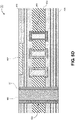
- FIG. 5B a cross-sectional illustration of the patch 505 after a magnetic plug 550 is provided in the hole 541 is shown, in accordance with an embodiment.
- the magnetic plug 550 may be in direct contact with the surfaces of the routing layers 513 and the core 512, as shown in Figure 5B .
- a conductive liner may be disposed over the surfaces of the hole 541 prior to disposing the magnetic plug 550. That is, in some embodiments, the magnetic plug 550 is separated from the routing layers 513 and the core 512 by a conductive layer, such as copper.
- the magnetic plug 550 may be dispensed with any suitable process, such as, but not limited to, paste printing.
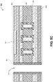
- FIG. 5C a cross-sectional illustration of the patch 505 after a second hole 542 is drilled through the magnetic plug 550 is shown, in accordance with an embodiment.
- the drilling of the second hole 542 results in the plug 550 being transformed into a magnetic shell 551.
- the magnetic shell 551 may have an outer diameter that is substantially equal to the diameter of the hole 541.
- the plug 552 may be an optically clear material.
- the plug 552 may be disposed in the second hole 542 with a printing process or the like.
- the plug 552 and the magnetic shell 551 may structurally form a Faraday rotator 530.
- FIG. 5E a cross-sectional illustration of the patch 505 after a lens 553, a photonics die 525, and a compute die 520 are attached to the patch 505 is shown, in accordance with an embodiment.
- the lens 553 may be disposed over a bottom surface of the plug 552. The lens 553 allows for incoming optical signals to be focused in order to improve efficiency.
- the photonics die 525 and the compute die 520 may be attached to the patch 505 by interconnects 521.
- the interconnects are shown as solder balls, but it is to be appreciated that any FLI architecture may be used to connect the photonics die 525 and the compute die 520 to the patch 505.
- the photonics die 525 is communicative coupled to the compute die 520 by the bridge 527 embedded in the top routing layers 513.
- the photonics die 525 is positioned over the Faraday rotator 530. That is, the Faraday rotator 530 is within a footprint of the photonics die 525. As such, an optical signal passing through the Faraday rotator 530 may be optically coupled to a bottom surface of the photonics die 525.
- the patch 505 may be assembled with an electronic system, such as the electronic system 400 in Figure 4 . That is, the patch 505 may be arranged so that it overhangs an edge of an interposer. As such, room for attaching a connector (not shown in Figure 5E ) to lens 553 is provided.
- the optical signal is coupled to the photonics die through a Faraday rotator that is positioned below the photonics die.
- a Faraday rotator that is positioned below the photonics die.
- Such an architecture requires overhanging the patch substrate over an edge of the interposer.
- embodiments disclosed herein may also include providing the Faraday rotator above the photonics die. Examples of such embodiments are shown in Figures 6A-7D .
- the electronic system 600 comprises a board 601 and a package substrate 602 attached to the board 601 by interconnects 603. While shown as solder balls, the interconnects 603 may comprise any interconnect architecture, such as sockets.
- the interconnects 603 may comprise any interconnect architecture, such as sockets.
- one or more embedded bridges 627 may be provided in the package substrate 602. The bridges 627 provide high density routing to communicatively couple photonics dies 625 to a compute die 620. The photonics dies 625 and the compute die 620 may be coupled to the package substrate 602 by interconnects 621. Interconnects 621 may comprise any FLI architecture.
- an integrated heat spreader (IHS) 660 may be provided over the package substrate 602.
- the IHS 660 may be thermally coupled to the compute die 620.
- a thermal interface material (TIM) (not shown) may be provided between the IHS 660 and the compute die 620.
- Faraday rotators 630 may pass through the IHS 660 and be optically coupled to the photonics dies 625. That is, the Faraday rotators 630 may be optically coupled to a top surface of the photonics dies 625.
- the Faraday rotator 630 may comprise a tubular housing 671.
- a first polarizer 672 and a second polarizer 675 are provided in the housing 671.
- a magnetic shell 673 may be provided between the first polarizer 672 and the second polarizer 675.
- the magnetic shell 673 may be a permanent magnet in some embodiments.
- the first polarizer 672 and the second polarizer 675 have a diameter that is substantially equal to an inner diameter of the magnetic shell 673.
- the first polarizer 672 and the second polarizer 675 may be positioned within the magnetic shell 673.
- the first polarizer 672 and the second polarizer 675 may be on opposite ends of the magnetic shell 673 and be entirely outside the magnetic shell 673.
- an optically clear plug 674 may be provided within an inner diameter of the magnetic shell 673.
- the second polarizer 675 may be a vertical polarizer and the first polarizer 672 may be an angled polarizer (e.g., 45°). That is, the first polarizer 672 may be different than the second polarizer 675.
- the magnetic shell 673 has a magnetic field that modifies the orientation of the incoming vertically polarized light. For example, the magnetic shell 673 may result in 45° polarized light in some embodiments.
- a first lens 677 may be provided within the housing 671.
- the lens 677 improves optical coupling between the Faraday rotator 630 and the photonics die 625.
- a connector 676 is provided over and around an end of the housing 671.
- the connector 676 may be tubular and surround an end of the housing 671.
- the connector 676 may comprise a second lens 678 to focus optical signals coming into the Faraday rotator 630.
- the connector 676 may provide mechanical coupling of an optical fiber 679 to the Faraday rotator 630.
- FIG. 6B a cross-sectional illustration of an electronic system 600 is shown, in accordance with an additional embodiment.
- the electronic system 600 in Figure 6B is substantially similar to the electronic system 600 in Figure 6A , with the exception of there being a different magnet configuration in the Faraday rotator 630.
- a conductive coil 683 is provided between the first polarizer 672 and the second polarizer 675.
- the conductive coil 683 may be an electromagnet that is connected to a power source (not shown). Controlling the current that passes through the conductive coil 683 allows for a controllable magnetic field to be provided around the plug 674. As such, the incoming optical signal can have a tunable light polarization.
- the Faraday rotators are discrete components that are assembled with the electronic systems 600. However, it is to be appreciated that various components of the Faraday rotator may also be fabricated in-situ with the assembly of the photonics die. An example of such an embodiment is shown in Figures 7A-7D .
- FIG. 7A a cross-sectional illustration of a portion of a photonics die 725 embedded in a dielectric layer 781 is shown, in accordance with an embodiment.
- an opening 782 may be provided through the dielectric layer 781 to expose a top surface of the photonics die 725.
- the lens 785 may be disposed over the exposed top surface of the photonics die 725.
- the lens 785 may be formed by dispensing a liquid polymer droplet over the exposed top surface of the photonics die 725. The liquid polymer droplet may then be cured to lock in the shape of the lens 785.
- FIG. 7C a cross-sectional illustration of the photonics die 725 after a Faraday rotator 730 is attached is shown, in accordance with an embodiment.
- the Faraday rotator 730 may be attached to the dielectric layer 781 by an adhesive 786.
- typical die mounting processes may be used to attach the Faraday rotator 730 to the dielectric layer 781.
- the Faraday rotator 730 may comprise a housing 771.
- the housing 771 may be a tubular housing in some embodiments.
- a first polarizer 772 and a second polarizer 775 may be provided within the housing 771.
- a magnetic shell 773 may be provided between the first polarizer 772 and the second polarizer 775.
- the magnetic shell 773 may be a permanent magnet.
- the magnetic shell 773 may be replaced with a conductive coil, similar to the embodiment shown in Figure 6B .
- the magnetic shell 773 may be entirely between the first polarizer 772 and the second polarizer 775.
- the first polarizer 772 may be at a first end of the magnetic shell 773 and surrounded by the magnetic shell 773
- the second polarizer 775 may be at a second end of the magnetic shell 773 and surrounded by the magnetic shell 773.
- an optically clear plug 774 may be provided within the magnetic shell 773.
- the second polarizer 775 may be a vertical polarizer and the first polarizer 772 may be an angled polarizer (e.g., 45°). That is, the first polarizer 772 may be different than the second polarizer 775.
- the magnetic shell 773 has a magnetic field that modifies the orientation of the incoming vertically polarized light. For example, the magnetic shell 773 may result in 45° polarized light in some embodiments.
- FIG. 7D a cross-sectional illustration of the photonics die 725 after a connector 787 is disposed over the Faraday rotator 730 is shown, in accordance with an embodiment.
- the connector 787 may be tubular and fit around the housing 771.
- a lens 788 may be provided in the connector 787.
- a portion of the Faraday rotator 730 may pass through an IHS (not shown) above the photonics die 725. In other embodiments, the Faraday rotator 730 may be entirely below the IHS, with only an optical cable passing through the IHS.
- FIG 8 illustrates a computing device 800 in accordance with one implementation of the invention.
- the computing device 800 houses a board 802.
- the board 802 may include a number of components, including but not limited to a processor 804 and at least one communication chip 806.
- the processor 804 is physically and electrically coupled to the board 802.
- the at least one communication chip 806 is also physically and electrically coupled to the board 802.
- the communication chip 806 is part of the processor 804.
- volatile memory e.g., DRAM
- non-volatile memory e.g., ROM
- flash memory e.g., a graphics processor, a digital signal processor, a crypto processor, a chipset, an antenna, a display, a touchscreen display, a touchscreen controller, a battery, an audio codec, a video codec, a power amplifier, a global positioning system (GPS) device, a compass, an accelerometer, a gyroscope, a speaker, a camera, and a mass storage device (such as hard disk drive, compact disk (CD), digital versatile disk (DVD), and so forth).
- volatile memory e.g., DRAM
- non-volatile memory e.g., ROM
- flash memory e.g., a graphics processor, a digital signal processor, a crypto processor, a chipset, an antenna, a display, a touchscreen display, a touchscreen controller, a battery, an audio codec, a video codec,
- the communication chip 806 enables wireless communications for the transfer of data to and from the computing device 800.
- wireless and its derivatives may be used to describe circuits, devices, systems, methods, techniques, communications channels, etc., that may communicate data through the use of modulated electromagnetic radiation through a non-solid medium. The term does not imply that the associated devices do not contain any wires, although in some embodiments they might not.
- the communication chip 806 may implement any of a number of wireless standards or protocols, including but not limited to Wi-Fi (IEEE 802.11 family), WiMAX (IEEE 802.16 family), IEEE 802.20, long term evolution (LTE), Ev-DO, HSPA+, HSDPA+, HSUPA+, EDGE, GSM, GPRS, CDMA, TDMA, DECT, Bluetooth, derivatives thereof, as well as any other wireless protocols that are designated as 3G, 4G, 5G, and beyond.
- the computing device 800 may include a plurality of communication chips 806.
- a first communication chip 806 may be dedicated to shorter range wireless communications such as Wi-Fi and Bluetooth and a second communication chip 806 may be dedicated to longer range wireless communications such as GPS, EDGE, GPRS, CDMA, WiMAX, LTE, Ev-DO, and others.
- the processor 804 of the computing device 800 includes an integrated circuit die packaged within the processor 804.
- the integrated circuit die of the processor may be part of an electronic system with a photonics die that is optically coupled to a Faraday rotator, in accordance with embodiments described herein.
- the term "processor" may refer to any device or portion of a device that processes electronic data from registers and/or memory to transform that electronic data into other electronic data that may be stored in registers and/or memory.
- the communication chip 806 also includes an integrated circuit die packaged within the communication chip 806.
- the integrated circuit die of the communication chip may be part of an electronic system with a photonics die that is optically coupled to a Faraday rotator, in accordance with embodiments described herein.
Landscapes
- Physics & Mathematics (AREA)
- General Physics & Mathematics (AREA)
- Optics & Photonics (AREA)
- Nonlinear Science (AREA)
- Engineering & Computer Science (AREA)
- Power Engineering (AREA)
- Optical Modulation, Optical Deflection, Nonlinear Optics, Optical Demodulation, Optical Logic Elements (AREA)
Abstract
Description
- Embodiments of the present disclosure relate to electronic packages, and more particularly to photonics packages with a Faraday rotator between an optical cable and the photonics die.
- The microelectronic industry has begun using optical connections as a way to increase bandwidth and performance. Typically, an optical fiber is coupled to a photonics die. The current coupling architectures include direct coupling between the interfaces. Such direct coupling does not fundamentally improve signal-to-noise ratios. In fact, these direct light coupling architectures may result in reflected light at the interface. The reflected light generates optical interference. The optical interference decreases the signal-to-noise ratio and can even result in inaccurate signals being propagated to the receivers.
-
-
Figure 1 is a schematic illustrating how a Faraday rotator functions, in accordance with an embodiment. -
Figure 2 is a cross-sectional illustration of a photonics package that comprises a Faraday rotator in a package on interposer (PoINT) architecture, in accordance with an embodiment. -
Figure 3A is a cross-sectional illustration of a patch with a through hole, in accordance with an embodiment. -
Figure 3B is a cross-sectional illustration of the patch after a Faraday rotator is inserted into the through hole, in accordance with an embodiment. -
Figure 3C is a cross-sectional illustration of the patch after a thermal treatment that expands a dielectric to mechanically couple the Faraday rotator to the patch, in accordance with an embodiment. -
Figure 3D is a cross-sectional illustration of the patch after a photonics die and a compute die are attached, in accordance with an embodiment. -
Figure 4 is a cross-sectional illustration of a photonics package that comprises an integrated Faraday rotator in a PoINT architecture, in accordance with an embodiment. -
Figure 5A is a cross-sectional illustration of a patch with a through hole, in accordance with an embodiment. -
Figure 5B is a cross-sectional illustration of the patch after a magnetic material is disposed in the through hole, in accordance with an embodiment. -
Figure 5C is a cross-sectional illustration of the patch after a through hole is formed through the magnetic material to form a magnetic shell, in accordance with an embodiment. -
Figure 5D is a cross-sectional illustration of the patch after an optically clear plug material is provided to fill the magnetic shell, in accordance with an embodiment. -
Figure 5E is a cross-sectional illustration of the patch after a compute die and a photonics die are attached, in accordance with an embodiment. -
Figure 6A is a cross-sectional illustration of a photonics package that comprises a Faraday rotator with a permanent magnetic shell, in accordance with an embodiment. -
Figure 6B is a cross-sectional illustration of a photonics package that comprises a Faraday rotator with an electromagnet coil, in accordance with an embodiment. -
Figure 7A is a cross-sectional illustration of a photonics die embedded in a package substrate with an opening through the package substrate to expose a surface of the photonics die, in accordance with an embodiment. -
Figure 7B is a cross-sectional illustration of the photonics die after a lens is formed over the exposed surface, in accordance with an embodiment. -
Figure 7C is a cross-sectional illustration of the photonics die after a Faraday rotator is attached to the package substrate over the lens, in accordance with an embodiment. -
Figure 7D is a cross-sectional illustration of the photonics die after a connector is attached over and around the Faraday rotator, in accordance with an embodiment. -
Figure 8 is a schematic of a computing device built in accordance with an embodiment. - Described herein are photonics packages with a Faraday rotator between an optical cable and the photonics die, in accordance with various embodiments. In the following description, various aspects of the illustrative implementations will be described using terms commonly employed by those skilled in the art to convey the substance of their work to others skilled in the art. However, it will be apparent to those skilled in the art that the present invention may be practiced with only some of the described aspects. For purposes of explanation, specific numbers, materials and configurations are set forth in order to provide a thorough understanding of the illustrative implementations. However, it will be apparent to one skilled in the art that the present invention may be practiced without the specific details. In other instances, well-known features are omitted or simplified in order not to obscure the illustrative implementations.
- Various operations will be described as multiple discrete operations, in turn, in a manner that is most helpful in understanding the present invention, however, the order of description should not be construed to imply that these operations are necessarily order dependent. In particular, these operations need not be performed in the order of presentation.
- As noted above, direct optical coupling between an optical cable and the photonics die leads to low signal-to-noise ratios. For example, reflections at the interface may be particularly problematic and leads to poor signal quality. Accordingly, embodiments disclosed herein include the integration of Faraday rotators into the photonics package architectures. An example schematic of the functioning of a Faraday
rotator 160 is shown inFigure 1 . - As shown in
Figure 1 , the Faradayrotator 160 comprises afirst polarizer 165, amagnetic region 166, and asecond polarizer 167 on the opposite side of themagnetic region 166 from thefirst polarizer 165. Incominglight 161 may have random polarization. After passing through thefirst polarizer 165, thelight 162 may be vertically polarized. In an embodiment, thelight 162 propagates through themagnetic region 166 where the magnetic field results in the polarization being shifted, as shown inlight 163. For example, a 45° polarization shift may be provided in some embodiments.Light 163 then passes through thesecond polarizer 167, which restricts light to only the selected polarization shift induced by themagnetic region 166, as shown bylight 164. In light passing the opposite direction (i.e.,light light magnetic region 166. Themagnetic region 166 again shifts the polarization. For example, when a 45° polarization is used, the polarization of thelight 169 is further shifted so thatlight 170 is 90° polarized. It is to be appreciated that such a Faraday architecture may result in the filtering out of reflections from the optical path. As such, the signal-to-noise ratio is increased, and performance of the optical interconnects are improved. - Referring now to
Figure 2 , a cross-sectional illustration of anelectronic system 200 is shown, in accordance with an embodiment. In an embodiment, theelectronic system 200 comprises a patch on interposer (PoINT) architecture. The PoINT architecture may comprise aboard 201. Theboard 201 may be a printed circuit board (PCB) or the like. In an embodiment, aninterposer 202 is attached to theboard 201 byinterconnects 203. Theinterconnects 203 are shown as being solder balls, but it is to be appreciated that any interconnect architecture may be used, such as sockets or the like. - In an embodiment, the
interposer 202 may comprise conductive routing (not shown). The conductive routing within theinterposer 202 may allow for conductive coupling between a top surface and a bottom surface of theinterposer 202. For example, the conductive routing may comprise pads, traces, vias, and the like. - In an embodiment, a
patch 205 is attached to theinterposer 202. For example, thepatch 205 may be coupled to theinterposer 202 byinterconnects 204, such as solder balls or the like. In an embodiment, thepatch 205 comprises acore 212 and conductive routing layers 213 above and below thecore 212. Through core vias 211 may conductively couple thetop routing layer 213 to thebottom routing layer 213. However, it is to be appreciated that in some embodiments, acoreless patch 205 may also be used. - In an embodiment, the
patch 205 may comprise a compute die 220 and aphotonics die 225. The compute die 220 may be any type of die, such as, but not limited to a processor, a graphics processor, a field-programmable gate array (FPGA), a system on a chip (SoC), a memory, or the like. In an embodiment, the photonics die 225 comprises features for converting signals between the optical regime and the electrical regime. For example, the photonics die 225 may comprise a laser and/or a photodiode. In an embodiment, the compute die 220 is communicatively coupled to the photonics die 225 by abridge 227 that is embedded in thetop routing layer 213 of thepatch 205. Thebridge 227 provides a dimensionally stable substrate on which high density conductive routing can be provided. - In an embodiment, the
patch 205 is arranged so that it overhangs an edge of theinterposer 202. For example, thepatch 205 inFigure 2 overhangs the left edge of theinterposer 202. Overhanging theinterposer 202 allows for a bottom surface of thepatch 205 to be exposed. Particularly, a space between theunderlying board 201 and the bottom surface of thepatch 205 is sufficient to provide an optical connection to the photonics die 225 from below. In a particular embodiment, anoptical cable 234 is connected to aconnector 233. Theconnector 233 interfaces with aFaraday rotator 230 that passes through a thickness of thepatch 205. In an embodiment, theFaraday rotator 230 is positioned within a footprint of the photonics die 225. As such, an optical path is provided through theFaraday rotator 230 from theconnector 233 to the photonics die 225. - In an embodiment, the
Faraday rotator 230 comprises a housing 232. The housing 232 may be a tube. In an embodiment, the housing 232 is mechanically coupled to thepatch 205 by adielectric layer 231. As will be described below, thedielectric layer 231 is a material that expands during a heat treatment. As such, theFaraday rotator 230 can be inserted into thepatch 205, and the heat treatment secures theFaraday rotator 230 to thepatch 205. - In an embodiment, the
Faraday rotator 230 may comprise afirst polarizer 236 and asecond polarizer 237. Thefirst polarizer 236 may be a vertical polarizer and thesecond polarizer 237 may be an angled polarizer (e.g., 45°). That is, thefirst polarizer 236 may be different than thesecond polarizer 237. In an embodiment, a magnetic region is provided between thefirst polarizer 236 and thesecond polarizer 237. The magnetic region may comprise apermanent magnet 235. Thepermanent magnet 235 may be a shell that wraps around an opticallyclear layer 238. Thepermanent magnet 235 has a magnetic field that modifies the orientation of the incoming vertically polarized light. For example, thepermanent magnet 235 may result in 45° polarized light in some embodiments. - In an embodiment, the efficiency of the
Faraday rotator 230 may be further improved by including lenses. For example, afirst lens 239A may be provided between thefirst polarizer 236 and theconnector 233, and asecond lens 239B may be provided between thesecond polarizer 237 and the photonics die 225. - Referring now to
Figures 3A-3D , a series of cross-sectional illustrations depicting a process for fabricating apatch 305 is shown, in accordance with an embodiment. Thepatch 305 inFigures 3A-3D may be substantially similar to thepatch 205 inFigure 2 . - Referring now to
Figure 3A , a cross-sectional illustration of apatch 305 is shown, in accordance with an embodiment. In an embodiment, thepatch 305 may comprise a core 312 with routinglayers 313 above and below thecore 312. Through core vias 311 may electrically couple thetop routing layers 313 to the bottom routing layers 313. In yet another embodiment, thepatch 305 may be coreless. In the illustrated embodiment, conductive traces are shown in the routing layers 313. However, it is to be appreciated that conductive vias, traces, and pads may be provided in the routing layers 313 in order to provide the necessary conductive routing. In an embodiment, abridge 327 for providing high density routing may also be provided in the top routing layers 313. - In an embodiment, a
hole 341 is formed through thepatch 305. Thehole 341 may be formed with any drilling process. For example, thehole 341 may be mechanically drilled or drilled with a laser. In the case of a laser drilled hole, the sidewalls of thehole 341 may be tapered, as is common in laser drilled architectures. Thehole 341 passes through thetop routing layers 313, thecore 312, and the bottom routing layers 313. That is, thehole 341 extends through an entire thickness of thepatch 305. - Referring now to
Figure 3B , a cross-sectional illustration of thepatch 305 afterFaraday rotator 330 is inserted into thehole 341 is shown, in accordance with an embodiment. In an embodiment, theFaraday rotator 330 comprise ahousing 332 that is tubular. An outer surface of thehousing 332 may be lined with adielectric material 331. In an initial state, the outer diameter of thedielectric material 331 may be smaller than a diameter of thehole 341. - In an embodiment, the
Faraday rotator 330 may comprise afirst polarizer 336 and asecond polarizer 337. Thefirst polarizer 336 may be a vertical polarizer and thesecond polarizer 337 may be an angled polarizer (e.g., 45°). That is, thefirst polarizer 336 may be different than thesecond polarizer 337. In an embodiment, a magnetic region is provided between thefirst polarizer 336 and thesecond polarizer 337. The magnetic region may comprise apermanent magnet 335. Thepermanent magnet 335 may be a shell that wraps around an opticallyclear layer 338. While shown as a physical layer inFigure 3B , it is to be appreciated that thepermanent magnet 335 may have an air core in some embodiments. Thepermanent magnet 335 has a magnetic field that modifies the orientation of the incoming vertically polarized light. For example, thepermanent magnet 335 may result in 45° polarized light in some embodiments. - In an embodiment, the
permanent magnet 335 may be in direct contact with thefirst polarizer 336 and thesecond polarizer 337. For example, a bottom surface of thepermanent magnet 335 may be in direct contact with a top surface of thefirst polarizer 336, and a top surface of thepermanent magnet 335 may be in direct contact with a bottom surface of thesecond polarizer 337. Thepermanent magnet 335 may have an outer diameter that is substantially equal to diameters of thefirst polarizer 336 and thesecond polarizer 337. - In an embodiment, the
Faraday rotator 330 may also comprise afirst lens 339A and asecond lens 339B. Thefirst lens 339A is within the housing below thefirst polarizer 336, and thesecond lens 339B is within the housing above thesecond polarizer 337. Thelenses Faraday rotator 330. - In the illustrated embodiment, the
first polarizer 336, thesecond polarizer 337, and thepermanent magnet 335 are positioned at approximately a midpoint of thehousing 332. That is, thefirst polarizer 336, thesecond polarizer 337, and thepermanent magnet 335 are positioned substantially within thecore 312 of thepatch 305. However, it is to be appreciated that thefirst polarizer 336, thesecond polarizer 337, and thepermanent magnet 335 may be positioned at any vertical location within thepatch 305. Additionally, while shown as be directly in contact with each other, embodiments may include spacings between one or more of thefirst polarizer 336, thesecond polarizer 337, and thepermanent magnet 335. - Referring now to
Figure 3C , a cross-sectional illustration of thepatch 305 after a thermal treatment is shown, in accordance with an embodiment. In an embodiment, the thermal treatment may be at an elevated temperature (e.g., 300°C or more) for a designated period of time. The heat treatment induces a physical change in thedielectric material 331. Particularly, an outer diameter of thedielectric material 331 is increased by the heat treatment. For example, the outer diameter of thedielectric material 331 may expand to completely fill thehole 341. As such, thedielectric material 331 mechanically couples theFaraday rotator 330 to thepatch 305. - Referring now to
Figure 3D , a cross-sectional illustration of thepatch 305 after a compute die 320 and a photonics die 325 are attached is shown, in accordance with an embodiment. In an embodiment, the compute die 320 and the photonics die 325 may be attached to the patch byinterconnects 321. While shown as solder balls, it is to be appreciated that theinterconnects 321 may be any first level interconnect (FLI). The photonics die 325 may be communicatively coupled to the compute die 320 by thebridge 327 in the top routing layers 313. In an embodiment, the photonics die 325 extends over theFaraday rotator 330. That is, theFaraday rotator 330 may be within a footprint of the photonics die 325. As such, optical signals propagating through theFaraday rotator 330 may be optically coupled to a bottom surface of the photonics die 325. - After attachment of the photonics die 325 and the compute die 320, the
patch 305 may be assembled with an electronic system, such as theelectronic system 200 inFigure 2 . That is, thepatch 305 may be arranged so that it overhangs an edge of an interposer. As such, room for attaching a connector (not shown inFigure 3D ) to a bottom of thehousing 332 is provided. - Referring now to
Figure 4 , a cross-sectional illustration of anelectronic system 400 is shown, in accordance with an additional embodiment. In an embodiment, theelectronic system 400 comprises aboard 401, such as a PCB. Aninterposer 402 is attached to theboard 401 byinterconnects 403. In an embodiment, apatch 405 is attached to theinterposer 402 byinterconnects 404. The system level architecture ofelectronic system 400 may be substantially similar to the system level architecture ofelectronic system 200 inFigure 2 . For example, thepatch 405 may overhang an edge of theunderlying interposer 402. - In an embodiment, the
patch 405 may comprise a core 412 with conductive routing layers 413 above and below thecore 412. Through core vias 411 may electrically couple thetop routing layers 413 to the bottom routing layers 413. In other embodiments, thepatch 405 may be coreless. In an embodiment, a compute die 420 and a photonics die 425 are attached to thepatch 405 byinterconnects 421.Interconnects 421 may be any suitable FLIs. The compute die 420 may be communicatively coupled to the photonics die 425 by abridge 427 embedded in the top routing layers 413. - In an embodiment, the
patch 405 comprises aFaraday rotator 430. TheFaraday rotator 430 may be integrated with thepatch 405. That is, instead of being a discrete component (as is the case inFigure 2 ), theFaraday rotator 430 is assembled as part of thepatch 405 during fabrication of thepatch 405. Such an integrated process is described in greater detail below. - In an embodiment, the
Faraday rotator 430 comprises amagnetic shell 451 and an opticallyclear core 452. Themagnetic shell 451 may be in direct contact with the routing layers 413 and thecore 412. That is, there may be no housing between themagnetic shell 451 and the substrate of thepatch 405. However, in other embodiments, a liner (not shown) may separate themagnetic shell 451 from the substrate of thepatch 405. In an embodiment, alens 453 may be provided at a bottom of theFaraday rotator 430. Thelens 453 may be coupled to anoptical cable 434. - While there are no polarizers shown in
Figure 4 , it is to be appreciated that embodiments may comprise a pair of polarizers provided on opposite ends of themagnetic shell 451. In other embodiments, theFaraday rotator 430 may be used without the polarizers. - Referring now to
Figures 5A-5E , a series of cross-sectional illustrations depicting a process for fabricating apatch 505 is shown, in accordance with an embodiment. Thepatch 505 inFigures 5A-5E may be substantially similar to thepatch 405 inFigure 4 . - Referring now to
Figure 5A , a cross-sectional illustration of apatch 505 is shown, in accordance with an embodiment. In an embodiment, thepatch 505 may comprise a core 512 with routinglayers 513 above and below thecore 512. Through core vias 511 may electrically couple thetop routing layers 513 to the bottom routing layers 513. In yet another embodiment, thepatch 505 may be coreless. In the illustrated embodiment, conductive traces are shown in the routing layers 513. However, it is to be appreciated that conductive vias, traces, and pads may be provided in the routing layers 513 in order to provide the necessary conductive routing. In an embodiment, abridge 527 for providing high density routing may also be provided in the top routing layers 513. - In an embodiment, a
hole 541 is formed through thepatch 505. Thehole 541 may be formed with any drilling process. For example, thehole 541 may be mechanically drilled or drilled with a laser. In the case of a laser drilled hole, the sidewalls of thehole 541 may be tapered, as is common in laser drilled architectures. Thehole 541 passes through thetop routing layers 513, thecore 512, and the bottom routing layers 513. That is, thehole 541 extends through an entire thickness of thepatch 505. - Referring now to
Figure 5B , a cross-sectional illustration of thepatch 505 after amagnetic plug 550 is provided in thehole 541 is shown, in accordance with an embodiment. In the illustrated embodiment, themagnetic plug 550 may be in direct contact with the surfaces of the routing layers 513 and thecore 512, as shown inFigure 5B . In other embodiments, a conductive liner may be disposed over the surfaces of thehole 541 prior to disposing themagnetic plug 550. That is, in some embodiments, themagnetic plug 550 is separated from the routing layers 513 and thecore 512 by a conductive layer, such as copper. In an embodiment, themagnetic plug 550 may be dispensed with any suitable process, such as, but not limited to, paste printing. - Referring now to
Figure 5C , a cross-sectional illustration of thepatch 505 after asecond hole 542 is drilled through themagnetic plug 550 is shown, in accordance with an embodiment. In an embodiment, the drilling of thesecond hole 542 results in theplug 550 being transformed into amagnetic shell 551. Themagnetic shell 551 may have an outer diameter that is substantially equal to the diameter of thehole 541. - Referring now to
Figure 5D , a cross-sectional illustration of thepatch 505 after aplug 552 is provided in thesecond hole 542 is shown, in accordance with an embodiment. In an embodiment, theplug 552 may be an optically clear material. In an embodiment, theplug 552 may be disposed in thesecond hole 542 with a printing process or the like. Theplug 552 and themagnetic shell 551 may structurally form aFaraday rotator 530. - Referring now to
Figure 5E , a cross-sectional illustration of thepatch 505 after alens 553, aphotonics die 525, and a compute die 520 are attached to thepatch 505 is shown, in accordance with an embodiment. In an embodiment, thelens 553 may be disposed over a bottom surface of theplug 552. Thelens 553 allows for incoming optical signals to be focused in order to improve efficiency. - In an embodiment, the photonics die 525 and the compute die 520 may be attached to the
patch 505 byinterconnects 521. The interconnects are shown as solder balls, but it is to be appreciated that any FLI architecture may be used to connect the photonics die 525 and the compute die 520 to thepatch 505. In an embodiment, the photonics die 525 is communicative coupled to the compute die 520 by thebridge 527 embedded in the top routing layers 513. In an embodiment, the photonics die 525 is positioned over theFaraday rotator 530. That is, theFaraday rotator 530 is within a footprint of the photonics die 525. As such, an optical signal passing through theFaraday rotator 530 may be optically coupled to a bottom surface of the photonics die 525. - After attachment of the photonics die 525 and the compute die 520, the
patch 505 may be assembled with an electronic system, such as theelectronic system 400 inFigure 4 . That is, thepatch 505 may be arranged so that it overhangs an edge of an interposer. As such, room for attaching a connector (not shown inFigure 5E ) tolens 553 is provided. - In
Figures 2-5E , the optical signal is coupled to the photonics die through a Faraday rotator that is positioned below the photonics die. Such an architecture requires overhanging the patch substrate over an edge of the interposer. However, embodiments are not limited to such architectures. For example, embodiments disclosed herein may also include providing the Faraday rotator above the photonics die. Examples of such embodiments are shown inFigures 6A-7D . - Referring now to
Figure 6A , a cross-sectional illustration of anelectronic system 600 is shown, in accordance with an embodiment. In an embodiment, theelectronic system 600 comprises aboard 601 and apackage substrate 602 attached to theboard 601 byinterconnects 603. While shown as solder balls, theinterconnects 603 may comprise any interconnect architecture, such as sockets. In an embodiment, one or more embeddedbridges 627 may be provided in thepackage substrate 602. Thebridges 627 provide high density routing to communicatively couple photonics dies 625 to acompute die 620. The photonics dies 625 and the compute die 620 may be coupled to thepackage substrate 602 byinterconnects 621.Interconnects 621 may comprise any FLI architecture. In an embodiment, an integrated heat spreader (IHS) 660 may be provided over thepackage substrate 602. TheIHS 660 may be thermally coupled to the compute die 620. For example, a thermal interface material (TIM) (not shown) may be provided between theIHS 660 and the compute die 620. - In an embodiment,
Faraday rotators 630 may pass through theIHS 660 and be optically coupled to the photonics dies 625. That is, theFaraday rotators 630 may be optically coupled to a top surface of the photonics dies 625. In an embodiment, theFaraday rotator 630 may comprise atubular housing 671. Afirst polarizer 672 and asecond polarizer 675 are provided in thehousing 671. Amagnetic shell 673 may be provided between thefirst polarizer 672 and thesecond polarizer 675. Themagnetic shell 673 may be a permanent magnet in some embodiments. In the illustrated embodiment, thefirst polarizer 672 and thesecond polarizer 675 have a diameter that is substantially equal to an inner diameter of themagnetic shell 673. In such an embodiment, thefirst polarizer 672 and thesecond polarizer 675 may be positioned within themagnetic shell 673. However, in other embodiments, thefirst polarizer 672 and thesecond polarizer 675 may be on opposite ends of themagnetic shell 673 and be entirely outside themagnetic shell 673. In an embodiment, an opticallyclear plug 674 may be provided within an inner diameter of themagnetic shell 673. - The
second polarizer 675 may be a vertical polarizer and thefirst polarizer 672 may be an angled polarizer (e.g., 45°). That is, thefirst polarizer 672 may be different than thesecond polarizer 675. In an embodiment, themagnetic shell 673 has a magnetic field that modifies the orientation of the incoming vertically polarized light. For example, themagnetic shell 673 may result in 45° polarized light in some embodiments. - In an embodiment, a
first lens 677 may be provided within thehousing 671. Thelens 677 improves optical coupling between theFaraday rotator 630 and the photonics die 625. In an embodiment, aconnector 676 is provided over and around an end of thehousing 671. Theconnector 676 may be tubular and surround an end of thehousing 671. Theconnector 676 may comprise asecond lens 678 to focus optical signals coming into theFaraday rotator 630. Theconnector 676 may provide mechanical coupling of anoptical fiber 679 to theFaraday rotator 630. - Referring now to
Figure 6B , a cross-sectional illustration of anelectronic system 600 is shown, in accordance with an additional embodiment. In an embodiment, theelectronic system 600 inFigure 6B is substantially similar to theelectronic system 600 inFigure 6A , with the exception of there being a different magnet configuration in theFaraday rotator 630. Instead of providing a permanent magnet shell, aconductive coil 683 is provided between thefirst polarizer 672 and thesecond polarizer 675. Theconductive coil 683 may be an electromagnet that is connected to a power source (not shown). Controlling the current that passes through theconductive coil 683 allows for a controllable magnetic field to be provided around theplug 674. As such, the incoming optical signal can have a tunable light polarization. - In
Figures 6A and6B , the Faraday rotators are discrete components that are assembled with theelectronic systems 600. However, it is to be appreciated that various components of the Faraday rotator may also be fabricated in-situ with the assembly of the photonics die. An example of such an embodiment is shown inFigures 7A-7D . - Referring now to
Figure 7A , a cross-sectional illustration of a portion of a photonics die 725 embedded in adielectric layer 781 is shown, in accordance with an embodiment. In an embodiment, anopening 782 may be provided through thedielectric layer 781 to expose a top surface of the photonics die 725. - Referring now to
Figure 7B , a cross-sectional illustration of the photonics die 725 after alens 785 is formed is shown, in accordance with an embodiment. In an embodiment, thelens 785 may be disposed over the exposed top surface of the photonics die 725. Thelens 785 may be formed by dispensing a liquid polymer droplet over the exposed top surface of the photonics die 725. The liquid polymer droplet may then be cured to lock in the shape of thelens 785. - Referring now to
Figure 7C , a cross-sectional illustration of the photonics die 725 after aFaraday rotator 730 is attached is shown, in accordance with an embodiment. In an embodiment, theFaraday rotator 730 may be attached to thedielectric layer 781 by an adhesive 786. For example, typical die mounting processes may be used to attach theFaraday rotator 730 to thedielectric layer 781. - In an embodiment, the
Faraday rotator 730 may comprise ahousing 771. Thehousing 771 may be a tubular housing in some embodiments. Afirst polarizer 772 and asecond polarizer 775 may be provided within thehousing 771. In an embodiment, amagnetic shell 773 may be provided between thefirst polarizer 772 and thesecond polarizer 775. Themagnetic shell 773 may be a permanent magnet. However, in other embodiments, themagnetic shell 773 may be replaced with a conductive coil, similar to the embodiment shown inFigure 6B . In an embodiment, themagnetic shell 773 may be entirely between thefirst polarizer 772 and thesecond polarizer 775. In other embodiments, thefirst polarizer 772 may be at a first end of themagnetic shell 773 and surrounded by themagnetic shell 773, and thesecond polarizer 775 may be at a second end of themagnetic shell 773 and surrounded by themagnetic shell 773. In an embodiment, an opticallyclear plug 774 may be provided within themagnetic shell 773. - The
second polarizer 775 may be a vertical polarizer and thefirst polarizer 772 may be an angled polarizer (e.g., 45°). That is, thefirst polarizer 772 may be different than thesecond polarizer 775. In an embodiment, themagnetic shell 773 has a magnetic field that modifies the orientation of the incoming vertically polarized light. For example, themagnetic shell 773 may result in 45° polarized light in some embodiments. - Referring now to
Figure 7D , a cross-sectional illustration of the photonics die 725 after aconnector 787 is disposed over theFaraday rotator 730 is shown, in accordance with an embodiment. Theconnector 787 may be tubular and fit around thehousing 771. In an embodiment, alens 788 may be provided in theconnector 787. - In an embodiment, a portion of the
Faraday rotator 730 may pass through an IHS (not shown) above the photonics die 725. In other embodiments, theFaraday rotator 730 may be entirely below the IHS, with only an optical cable passing through the IHS. -
Figure 8 illustrates acomputing device 800 in accordance with one implementation of the invention. Thecomputing device 800 houses aboard 802. Theboard 802 may include a number of components, including but not limited to aprocessor 804 and at least onecommunication chip 806. Theprocessor 804 is physically and electrically coupled to theboard 802. In some implementations the at least onecommunication chip 806 is also physically and electrically coupled to theboard 802. In further implementations, thecommunication chip 806 is part of theprocessor 804. - These other components include, but are not limited to, volatile memory (e.g., DRAM), non-volatile memory (e.g., ROM), flash memory, a graphics processor, a digital signal processor, a crypto processor, a chipset, an antenna, a display, a touchscreen display, a touchscreen controller, a battery, an audio codec, a video codec, a power amplifier, a global positioning system (GPS) device, a compass, an accelerometer, a gyroscope, a speaker, a camera, and a mass storage device (such as hard disk drive, compact disk (CD), digital versatile disk (DVD), and so forth).
- The
communication chip 806 enables wireless communications for the transfer of data to and from thecomputing device 800. The term "wireless" and its derivatives may be used to describe circuits, devices, systems, methods, techniques, communications channels, etc., that may communicate data through the use of modulated electromagnetic radiation through a non-solid medium. The term does not imply that the associated devices do not contain any wires, although in some embodiments they might not. Thecommunication chip 806 may implement any of a number of wireless standards or protocols, including but not limited to Wi-Fi (IEEE 802.11 family), WiMAX (IEEE 802.16 family), IEEE 802.20, long term evolution (LTE), Ev-DO, HSPA+, HSDPA+, HSUPA+, EDGE, GSM, GPRS, CDMA, TDMA, DECT, Bluetooth, derivatives thereof, as well as any other wireless protocols that are designated as 3G, 4G, 5G, and beyond. Thecomputing device 800 may include a plurality ofcommunication chips 806. For instance, afirst communication chip 806 may be dedicated to shorter range wireless communications such as Wi-Fi and Bluetooth and asecond communication chip 806 may be dedicated to longer range wireless communications such as GPS, EDGE, GPRS, CDMA, WiMAX, LTE, Ev-DO, and others. - The
processor 804 of thecomputing device 800 includes an integrated circuit die packaged within theprocessor 804. In some implementations of the invention, the integrated circuit die of the processor may be part of an electronic system with a photonics die that is optically coupled to a Faraday rotator, in accordance with embodiments described herein. The term "processor" may refer to any device or portion of a device that processes electronic data from registers and/or memory to transform that electronic data into other electronic data that may be stored in registers and/or memory. - The
communication chip 806 also includes an integrated circuit die packaged within thecommunication chip 806. In accordance with another implementation of the invention, the integrated circuit die of the communication chip may be part of an electronic system with a photonics die that is optically coupled to a Faraday rotator, in accordance with embodiments described herein. - The above description of illustrated implementations of the invention, including what is described in the Abstract, is not intended to be exhaustive or to limit the invention to the precise forms disclosed. While specific implementations of, and examples for, the invention are described herein for illustrative purposes, various equivalent modifications are possible within the scope of the invention, as those skilled in the relevant art will recognize.
- These modifications may be made to the invention in light of the above detailed description. The terms used in the following claims should not be construed to limit the invention to the specific implementations disclosed in the specification and the claims. Rather, the scope of the invention is to be determined entirely by the following claims, which are to be construed in accordance with established doctrines of claim interpretation.
- Example 1: a photonics package, comprising: an interposer; a patch over the interposer, wherein the patch overhangs an edge of the interposer; a photonics die on the patch; and a Faraday rotator passing through a thickness of the patch, wherein the Faraday rotator is below the photonics die.
- Example 2: the photonics package of Example 1, wherein the Faraday rotator comprises: a tube; a first polarizer in the tube; a second polarizer in the tube; and a magnetic region between the first polarizer and the second polarizer.
- Example 3: the photonics package of Example 2, wherein the Faraday rotator further comprises: a first lens in the tube; and a second lens in the tube, wherein the first polarizer and the second polarizer are between the first lens and the second lens.
- Example 4: the photonics package of Example 2 or Example 3, further comprising: a connector over an end of the tube; and an optical cable coupled to the connector.
- Example 5: the photonics package of Example 4, wherein the connector is on a surface of the patch opposite from the photonics die.
- Example 6: the photonics package of Examples 2-5, further comprising: a dielectric shell around the tube, wherein the dielectric shell mechanically couples the tube to the patch.
- Example 7: the photonics package of Examples 1-6, further comprising:
an opening through the patch, wherein the Faraday rotator is provided in the opening. - Example 8: The photonics package of Example 7, wherein the Faraday rotator comprises: a magnetic shell in the opening; and an optically clear plug within the magnetic shell.
- Example 9: the photonics package of Example 8, further comprising: a lens over the optically clear plug on a surface of the patch opposite from the photonics die.
- Example 10: the photonics package of Example 9, further comprising: an optical cable connected to the lens.
- Example 11: the photonics package of Examples 1-10, further comprising: a compute die over the patch.
- Example 12: the photonics package of Example 11, wherein the compute die is communicatively coupled to the photonics die by a bridge embedded in the patch.
- Example 13: a patch for an electronic package, wherein the patch comprises: a patch substrate, wherein the patch substrate comprises a core and routing layers above and below the core; and a Faraday rotator passing through a thickness of the patch substrate.
- Example 14: the patch of Example 13, wherein the Faraday rotator comprises: a tube; a first polarizer in the tube; a second polarizer in the tube; and a magnetic region between the first polarizer and the second polarizer.
- Example 15: the patch of Example 13, wherein the Faraday rotator comprises: a magnetic shell passing through the thickness of the patch substrate; and an optically clear plug filling the interior of the magnetic shell.
- Example 16: the patch of Examples 13-15, further comprising: a photonics die over the patch substrate, wherein the photonics die is above the Faraday rotator.
- Example 17: the patch of Example 16, further comprising: a compute die over the patch substrate, wherein the compute die is communicatively coupled to the photonics die by a bridge embedded in the patch substrate.
- Example 18: an electronic system, comprising: a board; an interposer over the board; a patch over the interposer, wherein the patch overhangs an edge of the interposer; a photonics die over the patch; a compute die over the patch, wherein the compute die is communicatively coupled to the photonics die by a bridge embedded in the patch; and a Faraday rotator passing through a thickness of the patch.
- Example 19: the electronic system of Example 18, wherein the Faraday rotator comprises: a tube; a first polarizer in the tube; a second polarizer in the tube; and a magnetic region between the first polarizer and the second polarizer.
- Example 20: the electronic system of Example 18, wherein the Faraday rotator comprises: a magnetic shell passing through the thickness of the patch; and an optically clear plug filling the interior of the magnetic shell.
Claims (15)
- A photonics package, comprising:an interposer;a patch over the interposer, wherein the patch overhangs an edge of the interposer;a photonics die on the patch; anda Faraday rotator passing through a thickness of the patch, wherein the Faraday rotator is below the photonics die.
- The photonics package of claim 1, wherein the Faraday rotator comprises:a tube;a first polarizer in the tube;a second polarizer in the tube; anda magnetic region between the first polarizer and the second polarizer.
- The photonics package of claim 2, wherein the Faraday rotator further comprises:a first lens in the tube; anda second lens in the tube, wherein the first polarizer and the second polarizer are between the first lens and the second lens.
- The photonics package of claim 2 or 3, further comprising:a connector over an end of the tube; andan optical cable coupled to the connector.
- The photonics package of claim 4, wherein the connector is on a surface of the patch opposite from the photonics die.
- The photonics package of claim 2, 3, 4 or 5, further comprising:
a dielectric shell around the tube, wherein the dielectric shell mechanically couples the tube to the patch. - The photonics package of claim 1, 2, 3, 4, 5 or 6, further comprising:
an opening through the patch, wherein the Faraday rotator is provided in the opening. - The photonics package of claim 7, wherein the Faraday rotator comprises:a magnetic shell in the opening; andan optically clear plug within the magnetic shell.
- The photonics package of claim 8, further comprising:
a lens over the optically clear plug on a surface of the patch opposite from the photonics die. - The photonics package of claim 9, further comprising:
an optical cable connected to the lens. - A method of fabricating a photonics package, the method comprising:coupling a patch and an interposer, wherein the patch overhangs an edge of the interposer;coupling a photonics die and the patch; andforming a Faraday rotator passing through a thickness of the patch, wherein the Faraday rotator is below the photonics die.
- The method of claim 11, wherein the Faraday rotator comprises:a tube;a first polarizer in the tube;a second polarizer in the tube; anda magnetic region between the first polarizer and the second polarizer.
- The method of claim 12, wherein the Faraday rotator further comprises:a first lens in the tube; anda second lens in the tube, wherein the first polarizer and the second polarizer are between the first lens and the second lens.
- The method of claim 12 or 13, further comprising:coupling a connector and an end of the tube; andcoupling an optical cable to the connector.
- The method of claim 14, wherein the connector is on a surface of the patch opposite from the photonics die.
Applications Claiming Priority (1)
| Application Number | Priority Date | Filing Date | Title |
|---|---|---|---|
| US17/122,340 US12481108B2 (en) | 2020-12-15 | 2020-12-15 | Faraday rotator interconnect as a through-via configuration in a patch architecture |
Publications (2)
| Publication Number | Publication Date |
|---|---|
| EP4016151A1 true EP4016151A1 (en) | 2022-06-22 |
| EP4016151B1 EP4016151B1 (en) | 2025-04-16 |
Family
ID=77910622
Family Applications (1)
| Application Number | Title | Priority Date | Filing Date |
|---|---|---|---|
| EP21198382.0A Active EP4016151B1 (en) | 2020-12-15 | 2021-09-22 | Faraday rotator interconnect as a through-via configuration in a patch architecture |
Country Status (3)
| Country | Link |
|---|---|
| US (1) | US12481108B2 (en) |
| EP (1) | EP4016151B1 (en) |
| CN (1) | CN114639667A (en) |
Families Citing this family (5)
| Publication number | Priority date | Publication date | Assignee | Title |
|---|---|---|---|---|
| US11488918B2 (en) * | 2018-10-31 | 2022-11-01 | Intel Corporation | Surface finishes with low rBTV for fine and mixed bump pitch architectures |
| US12368511B2 (en) * | 2020-12-11 | 2025-07-22 | Intel Corporation | Embedded faraday rotators and components for increasing bandwidth and/or reducing fiber count in photonics multi chip packages |
| US20220187549A1 (en) * | 2020-12-15 | 2022-06-16 | Intel Corporation | Faraday rotator optical interconnects for optical insulator in semiconductor substrate packaging |
| US12061371B2 (en) * | 2020-12-22 | 2024-08-13 | Intel Corporation | Patch on interposer architecture for low cost optical co-packaging |
| US20220291462A1 (en) * | 2021-03-11 | 2022-09-15 | Intel Corporation | Method to couple light using integrated heat spreader |
Citations (5)
| Publication number | Priority date | Publication date | Assignee | Title |
|---|---|---|---|---|
| US5577140A (en) * | 1994-02-22 | 1996-11-19 | Pioneer Electronic Corporation | Optical coupling with electric field rotation |
| EP1168021A2 (en) * | 2000-06-26 | 2002-01-02 | Hitachi, Ltd. | Optical transmitter module |
| US20120314992A1 (en) * | 2011-06-07 | 2012-12-13 | Samsung Electronics Co., Ltd. | Electronic device having optical communicating part |
| US20140177625A1 (en) * | 2012-12-20 | 2014-06-26 | Peter L.D. Chang | Electro-optical assembly including a glass bridge |
| US20140321803A1 (en) * | 2013-04-26 | 2014-10-30 | Oracle International Corporation | Hybrid-integrated photonic chip package with an interposer |
Family Cites Families (5)
| Publication number | Priority date | Publication date | Assignee | Title |
|---|---|---|---|---|
| CA2502266A1 (en) * | 2004-03-26 | 2005-09-26 | Kyocera Corporation | External resonator and semiconductor laser module using the same |
| US7373033B2 (en) * | 2006-06-13 | 2008-05-13 | Intel Corporation | Chip-to-chip optical interconnect |
| US8168939B2 (en) * | 2008-07-09 | 2012-05-01 | Luxtera, Inc. | Method and system for a light source assembly supporting direct coupling to an integrated circuit |
| US9583912B2 (en) * | 2015-05-20 | 2017-02-28 | Hc Photonics Corp. | Compact optical and laser systems and ultrafast laser utilizing the same |
| US10243322B2 (en) * | 2015-12-17 | 2019-03-26 | Finisar Corporation | Surface coupled systems |
-
2020
- 2020-12-15 US US17/122,340 patent/US12481108B2/en active Active
-
2021
- 2021-09-22 EP EP21198382.0A patent/EP4016151B1/en active Active
- 2021-11-08 CN CN202111313488.XA patent/CN114639667A/en active Pending
Patent Citations (5)
| Publication number | Priority date | Publication date | Assignee | Title |
|---|---|---|---|---|
| US5577140A (en) * | 1994-02-22 | 1996-11-19 | Pioneer Electronic Corporation | Optical coupling with electric field rotation |
| EP1168021A2 (en) * | 2000-06-26 | 2002-01-02 | Hitachi, Ltd. | Optical transmitter module |
| US20120314992A1 (en) * | 2011-06-07 | 2012-12-13 | Samsung Electronics Co., Ltd. | Electronic device having optical communicating part |
| US20140177625A1 (en) * | 2012-12-20 | 2014-06-26 | Peter L.D. Chang | Electro-optical assembly including a glass bridge |
| US20140321803A1 (en) * | 2013-04-26 | 2014-10-30 | Oracle International Corporation | Hybrid-integrated photonic chip package with an interposer |
Non-Patent Citations (1)
| Title |
|---|
| CHANDRASEKHAR ARUN ET AL: "Server CPU Package Design Using PoINT Architecture", 2019 IEEE 69TH ELECTRONIC COMPONENTS AND TECHNOLOGY CONFERENCE (ECTC), IEEE, 28 May 2019 (2019-05-28), pages 2180 - 2185, XP033603932, DOI: 10.1109/ECTC.2019.00-20 * |
Also Published As
| Publication number | Publication date |
|---|---|
| EP4016151B1 (en) | 2025-04-16 |
| US12481108B2 (en) | 2025-11-25 |
| CN114639667A (en) | 2022-06-17 |
| US20220187548A1 (en) | 2022-06-16 |
Similar Documents
| Publication | Publication Date | Title |
|---|---|---|
| US12481108B2 (en) | Faraday rotator interconnect as a through-via configuration in a patch architecture | |
| EP4016150B1 (en) | Faraday rotator optical interconnects for optical insulator in semiconductor substrate packaging | |
| JP7832189B2 (en) | High-bandwidth optical interconnect architecture | |
| EP4057038A1 (en) | Method to couple light using integrated heat spreader | |
| US20250317206A1 (en) | Embedded faraday rotators and components for increasing bandwidth and/or reducing fiber count in photonics multi chip packages | |
| EP4020532A2 (en) | Assembly of 2xd module using high density interconnect bridges | |
| KR20210116202A (en) | Active bridge enabled co-packaged photonic transceiver | |
| NL2029788B1 (en) | Patch on interposer architecture for low cost optical co-packaging | |
| US9706092B1 (en) | Imager module with castellated interposer chip | |
| EP4020040A1 (en) | Novel connector designs for photonics packaging integration | |
| EP4063926A1 (en) | Enabling passive alignment for lens attach | |
| US20230204878A1 (en) | Photonics package including optic plug receptacle with support portion for photonics integrated circuit and lens assembly | |
| WO2023048813A1 (en) | Glass substrate embedded pic to pic and off-chip photonic communications | |
| US20230208010A1 (en) | 3d arrayed glass-based mmwave and thz structures | |
| US12573744B2 (en) | Wideband antennas in glass through direct via feeding and glass stacking | |
| US20240087971A1 (en) | Copper clad laminate (ccl) for plating pads within a glass cavity for glass core applications | |
| CN114175241A (en) | Monolithic die with acoustic resonator and active circuit | |
| EP4109497A1 (en) | Angled interconnect using glass core technology | |
| US20230314733A1 (en) | Self-docking self-aligned optical pcb connector for semiconductor packages | |
| US20220407216A1 (en) | In-package mmwave antennas and launchers using glass core technology | |
| US20240203805A1 (en) | Embedded memory for glass core packages | |
| US20250004219A1 (en) | Architecture and method for passive-active optical alignment of photonic integrated circuit (pic) and fiber array unit (fau) | |
| WO2022178825A1 (en) | Novel design for fiber array unit (fau) for optical transceiver products | |
| US20230207408A1 (en) | Suspended structures in glass using modified glass patterning processes | |
| US20240361541A1 (en) | Apparatus and methods for optical alignment for photonic integrated circuits |
Legal Events
| Date | Code | Title | Description |
|---|---|---|---|
| PUAI | Public reference made under article 153(3) epc to a published international application that has entered the european phase |
Free format text: ORIGINAL CODE: 0009012 |
|
| STAA | Information on the status of an ep patent application or granted ep patent |
Free format text: STATUS: THE APPLICATION HAS BEEN PUBLISHED |
|
| AK | Designated contracting states |
Kind code of ref document: A1 Designated state(s): AL AT BE BG CH CY CZ DE DK EE ES FI FR GB GR HR HU IE IS IT LI LT LU LV MC MK MT NL NO PL PT RO RS SE SI SK SM TR |
|
| STAA | Information on the status of an ep patent application or granted ep patent |
Free format text: STATUS: REQUEST FOR EXAMINATION WAS MADE |
|
| 17P | Request for examination filed |
Effective date: 20221222 |
|
| RBV | Designated contracting states (corrected) |
Designated state(s): AL AT BE BG CH CY CZ DE DK EE ES FI FR GB GR HR HU IE IS IT LI LT LU LV MC MK MT NL NO PL PT RO RS SE SI SK SM TR |
|
| GRAP | Despatch of communication of intention to grant a patent |
Free format text: ORIGINAL CODE: EPIDOSNIGR1 |
|
| STAA | Information on the status of an ep patent application or granted ep patent |
Free format text: STATUS: GRANT OF PATENT IS INTENDED |
|
| INTG | Intention to grant announced |
Effective date: 20241112 |
|
| GRAS | Grant fee paid |
Free format text: ORIGINAL CODE: EPIDOSNIGR3 |
|
| GRAA | (expected) grant |
Free format text: ORIGINAL CODE: 0009210 |
|
| STAA | Information on the status of an ep patent application or granted ep patent |
Free format text: STATUS: THE PATENT HAS BEEN GRANTED |
|
| AK | Designated contracting states |
Kind code of ref document: B1 Designated state(s): AL AT BE BG CH CY CZ DE DK EE ES FI FR GB GR HR HU IE IS IT LI LT LU LV MC MK MT NL NO PL PT RO RS SE SI SK SM TR |
|
| REG | Reference to a national code |
Ref country code: GB Ref legal event code: FG4D |
|
| REG | Reference to a national code |
Ref country code: CH Ref legal event code: EP Ref country code: DE Ref legal event code: R096 Ref document number: 602021029161 Country of ref document: DE |
|
| REG | Reference to a national code |
Ref country code: IE Ref legal event code: FG4D |
|
| P01 | Opt-out of the competence of the unified patent court (upc) registered |
Free format text: CASE NUMBER: APP_20035/2025 Effective date: 20250428 |
|
| REG | Reference to a national code |
Ref country code: NL Ref legal event code: FP |
|
| PGFP | Annual fee paid to national office [announced via postgrant information from national office to epo] |
Ref country code: NL Payment date: 20250704 Year of fee payment: 5 |
|
| REG | Reference to a national code |
Ref country code: AT Ref legal event code: MK05 Ref document number: 1786106 Country of ref document: AT Kind code of ref document: T Effective date: 20250416 |
|
| PG25 | Lapsed in a contracting state [announced via postgrant information from national office to epo] |
Ref country code: ES Free format text: LAPSE BECAUSE OF FAILURE TO SUBMIT A TRANSLATION OF THE DESCRIPTION OR TO PAY THE FEE WITHIN THE PRESCRIBED TIME-LIMIT Effective date: 20250416 Ref country code: PT Free format text: LAPSE BECAUSE OF FAILURE TO SUBMIT A TRANSLATION OF THE DESCRIPTION OR TO PAY THE FEE WITHIN THE PRESCRIBED TIME-LIMIT Effective date: 20250818 Ref country code: FI Free format text: LAPSE BECAUSE OF FAILURE TO SUBMIT A TRANSLATION OF THE DESCRIPTION OR TO PAY THE FEE WITHIN THE PRESCRIBED TIME-LIMIT Effective date: 20250416 |
|
| PGFP | Annual fee paid to national office [announced via postgrant information from national office to epo] |
Ref country code: DE Payment date: 20250819 Year of fee payment: 5 |
|
| REG | Reference to a national code |
Ref country code: LT Ref legal event code: MG9D |
|
| PG25 | Lapsed in a contracting state [announced via postgrant information from national office to epo] |
Ref country code: NO Free format text: LAPSE BECAUSE OF FAILURE TO SUBMIT A TRANSLATION OF THE DESCRIPTION OR TO PAY THE FEE WITHIN THE PRESCRIBED TIME-LIMIT Effective date: 20250716 Ref country code: GR Free format text: LAPSE BECAUSE OF FAILURE TO SUBMIT A TRANSLATION OF THE DESCRIPTION OR TO PAY THE FEE WITHIN THE PRESCRIBED TIME-LIMIT Effective date: 20250717 |
|
| PG25 | Lapsed in a contracting state [announced via postgrant information from national office to epo] |
Ref country code: PL Free format text: LAPSE BECAUSE OF FAILURE TO SUBMIT A TRANSLATION OF THE DESCRIPTION OR TO PAY THE FEE WITHIN THE PRESCRIBED TIME-LIMIT Effective date: 20250416 |
|
| PG25 | Lapsed in a contracting state [announced via postgrant information from national office to epo] |
Ref country code: BG Free format text: LAPSE BECAUSE OF FAILURE TO SUBMIT A TRANSLATION OF THE DESCRIPTION OR TO PAY THE FEE WITHIN THE PRESCRIBED TIME-LIMIT Effective date: 20250416 |
|
| PGFP | Annual fee paid to national office [announced via postgrant information from national office to epo] |
Ref country code: GB Payment date: 20250821 Year of fee payment: 5 |
|
| PG25 | Lapsed in a contracting state [announced via postgrant information from national office to epo] |
Ref country code: HR Free format text: LAPSE BECAUSE OF FAILURE TO SUBMIT A TRANSLATION OF THE DESCRIPTION OR TO PAY THE FEE WITHIN THE PRESCRIBED TIME-LIMIT Effective date: 20250416 |
|
| PG25 | Lapsed in a contracting state [announced via postgrant information from national office to epo] |
Ref country code: AT Free format text: LAPSE BECAUSE OF FAILURE TO SUBMIT A TRANSLATION OF THE DESCRIPTION OR TO PAY THE FEE WITHIN THE PRESCRIBED TIME-LIMIT Effective date: 20250416 |
|
| PGFP | Annual fee paid to national office [announced via postgrant information from national office to epo] |
Ref country code: FR Payment date: 20250821 Year of fee payment: 5 |
|
| PG25 | Lapsed in a contracting state [announced via postgrant information from national office to epo] |
Ref country code: RS Free format text: LAPSE BECAUSE OF FAILURE TO SUBMIT A TRANSLATION OF THE DESCRIPTION OR TO PAY THE FEE WITHIN THE PRESCRIBED TIME-LIMIT Effective date: 20250716 |
|
| PG25 | Lapsed in a contracting state [announced via postgrant information from national office to epo] |
Ref country code: IS Free format text: LAPSE BECAUSE OF FAILURE TO SUBMIT A TRANSLATION OF THE DESCRIPTION OR TO PAY THE FEE WITHIN THE PRESCRIBED TIME-LIMIT Effective date: 20250816 |
|
| PG25 | Lapsed in a contracting state [announced via postgrant information from national office to epo] |
Ref country code: LV Free format text: LAPSE BECAUSE OF FAILURE TO SUBMIT A TRANSLATION OF THE DESCRIPTION OR TO PAY THE FEE WITHIN THE PRESCRIBED TIME-LIMIT Effective date: 20250416 |
|
| PG25 | Lapsed in a contracting state [announced via postgrant information from national office to epo] |
Ref country code: SM Free format text: LAPSE BECAUSE OF FAILURE TO SUBMIT A TRANSLATION OF THE DESCRIPTION OR TO PAY THE FEE WITHIN THE PRESCRIBED TIME-LIMIT Effective date: 20250416 Ref country code: DK Free format text: LAPSE BECAUSE OF FAILURE TO SUBMIT A TRANSLATION OF THE DESCRIPTION OR TO PAY THE FEE WITHIN THE PRESCRIBED TIME-LIMIT Effective date: 20250416 |
|
| REG | Reference to a national code |
Ref country code: DE Ref legal event code: R097 Ref document number: 602021029161 Country of ref document: DE |
|
| PG25 | Lapsed in a contracting state [announced via postgrant information from national office to epo] |
Ref country code: CZ Free format text: LAPSE BECAUSE OF FAILURE TO SUBMIT A TRANSLATION OF THE DESCRIPTION OR TO PAY THE FEE WITHIN THE PRESCRIBED TIME-LIMIT Effective date: 20250416 |
|
| PG25 | Lapsed in a contracting state [announced via postgrant information from national office to epo] |
Ref country code: EE Free format text: LAPSE BECAUSE OF FAILURE TO SUBMIT A TRANSLATION OF THE DESCRIPTION OR TO PAY THE FEE WITHIN THE PRESCRIBED TIME-LIMIT Effective date: 20250416 |
|
| PG25 | Lapsed in a contracting state [announced via postgrant information from national office to epo] |
Ref country code: RO Free format text: LAPSE BECAUSE OF FAILURE TO SUBMIT A TRANSLATION OF THE DESCRIPTION OR TO PAY THE FEE WITHIN THE PRESCRIBED TIME-LIMIT Effective date: 20250416 Ref country code: SK Free format text: LAPSE BECAUSE OF FAILURE TO SUBMIT A TRANSLATION OF THE DESCRIPTION OR TO PAY THE FEE WITHIN THE PRESCRIBED TIME-LIMIT Effective date: 20250416 |
|
| PG25 | Lapsed in a contracting state [announced via postgrant information from national office to epo] |
Ref country code: IT Free format text: LAPSE BECAUSE OF FAILURE TO SUBMIT A TRANSLATION OF THE DESCRIPTION OR TO PAY THE FEE WITHIN THE PRESCRIBED TIME-LIMIT Effective date: 20250416 |
|
| PLBE | No opposition filed within time limit |
Free format text: ORIGINAL CODE: 0009261 |
|
| STAA | Information on the status of an ep patent application or granted ep patent |
Free format text: STATUS: NO OPPOSITION FILED WITHIN TIME LIMIT |
|
| REG | Reference to a national code |
Ref country code: CH Ref legal event code: L10 Free format text: ST27 STATUS EVENT CODE: U-0-0-L10-L00 (AS PROVIDED BY THE NATIONAL OFFICE) Effective date: 20260225 |
|
| 26N | No opposition filed |
Effective date: 20260119 |