EP4016091A1 - Dispositif onduleur comprenant un dispositif de mesure de tension - Google Patents
Dispositif onduleur comprenant un dispositif de mesure de tension Download PDFInfo
- Publication number
- EP4016091A1 EP4016091A1 EP21213098.3A EP21213098A EP4016091A1 EP 4016091 A1 EP4016091 A1 EP 4016091A1 EP 21213098 A EP21213098 A EP 21213098A EP 4016091 A1 EP4016091 A1 EP 4016091A1
- Authority
- EP
- European Patent Office
- Prior art keywords
- voltage
- capacitor
- measuring device
- inverter
- switches
- Prior art date
- Legal status (The legal status is an assumption and is not a legal conclusion. Google has not performed a legal analysis and makes no representation as to the accuracy of the status listed.)
- Granted
Links
Images

Classifications
-
- H—ELECTRICITY
- H02—GENERATION; CONVERSION OR DISTRIBUTION OF ELECTRIC POWER
- H02M—APPARATUS FOR CONVERSION BETWEEN AC AND AC, BETWEEN AC AND DC, OR BETWEEN DC AND DC, AND FOR USE WITH MAINS OR SIMILAR POWER SUPPLY SYSTEMS; CONVERSION OF DC OR AC INPUT POWER INTO SURGE OUTPUT POWER; CONTROL OR REGULATION THEREOF
- H02M7/00—Conversion of AC power input into DC power output; Conversion of DC power input into AC power output
- H02M7/42—Conversion of DC power input into AC power output without possibility of reversal
- H02M7/44—Conversion of DC power input into AC power output without possibility of reversal by static converters
- H02M7/48—Conversion of DC power input into AC power output without possibility of reversal by static converters using discharge tubes with control electrode or semiconductor devices with control electrode
- H02M7/53—Conversion of DC power input into AC power output without possibility of reversal by static converters using discharge tubes with control electrode or semiconductor devices with control electrode using devices of a triode or transistor type requiring continuous application of a control signal
- H02M7/537—Conversion of DC power input into AC power output without possibility of reversal by static converters using discharge tubes with control electrode or semiconductor devices with control electrode using devices of a triode or transistor type requiring continuous application of a control signal using semiconductor devices only, e.g. single switched pulse inverters
- H02M7/5387—Conversion of DC power input into AC power output without possibility of reversal by static converters using discharge tubes with control electrode or semiconductor devices with control electrode using devices of a triode or transistor type requiring continuous application of a control signal using semiconductor devices only, e.g. single switched pulse inverters in a bridge configuration
-
- G—PHYSICS
- G01—MEASURING; TESTING
- G01R—MEASURING ELECTRIC VARIABLES; MEASURING MAGNETIC VARIABLES
- G01R19/00—Arrangements for measuring currents or voltages or for indicating presence or sign thereof
- G01R19/165—Indicating that current or voltage is either above or below a predetermined value or within or outside a predetermined range of values
- G01R19/16533—Indicating that current or voltage is either above or below a predetermined value or within or outside a predetermined range of values characterised by the application
- G01R19/16538—Indicating that current or voltage is either above or below a predetermined value or within or outside a predetermined range of values characterised by the application in AC or DC supplies
- G01R19/16547—Indicating that current or voltage is either above or below a predetermined value or within or outside a predetermined range of values characterised by the application in AC or DC supplies voltage or current in AC supplies
-
- G—PHYSICS
- G01—MEASURING; TESTING
- G01R—MEASURING ELECTRIC VARIABLES; MEASURING MAGNETIC VARIABLES
- G01R19/00—Arrangements for measuring currents or voltages or for indicating presence or sign thereof
-
- G—PHYSICS
- G01—MEASURING; TESTING
- G01R—MEASURING ELECTRIC VARIABLES; MEASURING MAGNETIC VARIABLES
- G01R19/00—Arrangements for measuring currents or voltages or for indicating presence or sign thereof
- G01R19/0084—Measuring voltage only
-
- G—PHYSICS
- G01—MEASURING; TESTING
- G01R—MEASURING ELECTRIC VARIABLES; MEASURING MAGNETIC VARIABLES
- G01R19/00—Arrangements for measuring currents or voltages or for indicating presence or sign thereof
- G01R19/165—Indicating that current or voltage is either above or below a predetermined value or within or outside a predetermined range of values
- G01R19/16504—Indicating that current or voltage is either above or below a predetermined value or within or outside a predetermined range of values characterised by the components employed
- G01R19/16523—Indicating that current or voltage is either above or below a predetermined value or within or outside a predetermined range of values characterised by the components employed using diodes, e.g. Zener diodes
Definitions
- the invention lies in the field of measuring currents and voltages.
- This inverter OM comprises four controllable power switches T1, T2, T3, T4 mounted in an H bridge.
- the H bridge comprises two branches B1 and B2 each comprising two switches connected in series.
- the first branch B1 comprises a first switch T1 and a second switch T2 connected in series via a first point P1 called the first midpoint.
- the second branch B2 comprises a third switch T3 and a fourth switch T4 connected in series via a second point P2 called the second midpoint.
- the inverter OM is provided with an output low-pass filter interconnecting the midpoints P1 and P2.
- the output filter includes an output inductor L connected in series with a capacitor C.
- the inverter When the inverter is controlled so that the supply voltage of a load Z mounted in parallel with capacitor C is the reference sinusoidal voltage, the voltage across the terminals of capacitor C is a low-frequency sinusoid and the current flowing in capacitor C a current is a triangular whose frequency is the switching frequency of the switches which is high compared to that of the voltage.
- the output voltage delivered by the inverter OM is measured by means of measuring the voltage, for example, by means of resistors, and the current is measured by a current transformer consisting of a primary winding , a secondary winding, a magnetic circuit and a low impedance load in series with the secondary winding allowing the current flowing in the primary to be measured with a transformation ratio.
- Current measurements and voltage are then summed in a weighted way through a summing amplifier.
- An object of the present invention is to provide a simplified solution.
- the measuring device comprises the first capacitor.
- the differentiator filter has a time constant less than ten times a predetermined maximum period of the input current.
- the invention also relates to an inverter device intended to transform a DC voltage into a single-phase voltage, the inverter device comprising a low-pass filter comprising a first capacitor and an inductor, the measuring device and four power switches mounted in a bridge in H comprising two branches each comprising two switches connected in series, a first midpoint connecting the two switches of a first of the two branches and a second midpoint connecting the two switches of a second of the two branches, the first midpoint being connected to a first terminal of the first capacitor via the inductor and the second midpoint being connected to a second terminal of the second capacitor.
- the inverter device advantageously comprises a regulator configured to control the switches as a function of the voltage delivered to the terminals of the first resistor.
- the invention relates to a measuring device making it possible to deliver a voltage corresponding to a superposition of a voltage applied to its terminals and of an image voltage of a current supplying a first capacitor.
- This measuring device makes it possible, in particular, to deliver a voltage corresponding to a weighted sum of a sinusoidal voltage applied to its terminals and of an image voltage of an alternating current, for example triangular, supplying the first capacitor and having a frequency very high compared to the frequency of the voltage applied to the terminals of the measuring device, that is to say greater than ten times the frequency of the voltage applied to its terminals.
- image voltage of a current is meant a voltage having the same form, phase and frequency as the current.
- This measuring device finds its utility in providing a measurement used to regulate a voltage of any form and frequency by means of power switches.
- This measuring device finds, for example, its usefulness in providing a command for controlling the power switches of a voltage inverter so as to regulate the voltage delivered by this inverter to the terminals of the first capacitor on a voltage reference sinusoidal, for example by PWM with hysteresis.
- the measuring device DM according to the invention is shown in [ Fig.2 ].
- the measuring device DM is connected in parallel with a user impedance Z of impedance value z which can, for example, be inductive, capacitive or resistive supplied by a voltage V z , for example an output voltage of an inverter.
- the measuring device is mounted in parallel with the first capacitor C1 of first capacitance c1.
- the first capacitor is connected to an inductor L.
- the capacitor and the inductor form an LC circuit called LC1 in the rest of the text.
- the first capacitance c1 is such that the product of the value of the inductance L and of the first capacitance c1 is less than ten times a maximum period T AC of the alternating part of the current intended to flow in the first capacitor C1 , that is to say the maximum period T AC of the current intended to flow in the first capacitor C1.
- the minimum frequency of the alternating part of the current intended to circulate in the inductance L is much higher than the resonance frequency of the circuit LC1 which makes it possible to obtain a current of low amplitude in the capacitor C1.
- the measuring device DM comprises a differentiating filter FD connected in parallel with the first capacitor C1 comprising a second capacitor C2 and a first resistor R1 connected in series with the second capacitor C2.
- Differentiator filter FD has a time constant less than ten times a maximum period T AC of the alternating part of the current intended to flow in inductance L.
- the time constant of the differentiator filter is less than ten times the maximum period T AC of the current intended to flow in inductance L.
- r1 is the value of the first resistor R1 and c2 is the capacitance of the second capacitor C2.
- the measuring device DM further comprises a second resistor R2 of value r2 connected in parallel with the second capacitor C2 so that the first resistor R1 and the second resistor R2 form a voltage divider.
- the differentiator filter FD makes it possible to obtain, at the output of the differentiator filter FD, a voltage which is an image of a derivative of the voltage applied to the terminals of the differentiator filter FD which is the voltage applied to the terminals of the first capacitor. This voltage is therefore the image of the current I DM flowing in the first capacitor C1.
- the voltage divider makes it possible to divide the voltage applied at the input of the first capacitor C1 which is the input voltage of the measuring device DM.
- the voltage V mes delivered at the output of the measuring device DM is a weighted sum of an image voltage of the current I DM supplying the measuring device DM , that is to say of the current flowing in the first capacitor C1 (this image voltage is obtained by the differentiating filter) and of the voltage applied to the terminals of the measuring device V z , that is to say of the voltage applied to the terminals of the first capacitor C1 (obtained by the voltage divider).
- V my r 1 * vs 2 vs 1 ⁇ I DM + r 1 r 1 + r 2 ⁇ V z
- V z which is the voltage applied to the input terminals of the measuring device DM is also the voltage measured at the terminals of the user impedance Z which is, for example, the output voltage of a voltage inverter.
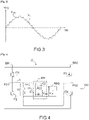
- V mes measured across the terminals of the first resistor R1 is shown in picture 3 in solid lines, in the case where the measuring device is connected to the output of a voltage inverter.
- the desired reference voltage at the output of capacitor V ref is a sinusoidal voltage shown in dotted lines.
- the voltage V mes is substantially the superposition of a sinusoidal voltage V ref and an alternating voltage in triangle image of the supply current of the first capacitor.
- the measuring device has the advantage of comprising only passive components. It is simple, inexpensive and has a relatively low mass. This allows its easy integration into an inverter device, for example, to ensure the regulation of a low or high power voltage inverter.
- this measuring device DM has the advantage of having no magnetic element. This makes it possible to avoid the problems linked to the saturation of the magnetic material, in particular the non-linearity of the measurement.
- the invention also relates to an inverter device comprising a single-phase inverter intended to transform a DC voltage into a single-phase voltage.
- the inverter O comprises four controllable power switches IT1, IT2, IT3, IT4 mounted in an H bridge.
- the H bridge comprises two branches BR1 and BR2 each comprising two switches connected in series.
- the first branch BR1 comprises a first switch IT1 and a second switch IT2 connected in series via a first point PO1 called the first midpoint.
- the second branch BR2 comprises a third switch IT3 and a fourth switch IT4 connected in series via a second point PO2 called the second midpoint.
- the inverter O also includes an output low-pass filter formed by the first capacitor C1 and the inductance L. Voltage inverters usually include this type of low-pass filter.
- the first capacitor C1 makes it possible to eliminate the DC component of the voltage and the inductance L makes it possible to control the level and the variations of the current I LOAD circulating in the line comprising the inductance
- the first midpoint PO1 is linked to a first terminal of the first capacitor C1 via the inductance L and the second midpoint PO2 is linked to a second terminal of the first capacitor C1.
- the period T AC mentioned above is the switching period of the switches.
- the period of the alternating part of the current flowing in the inductor L is equal to the switching period of the switches.
- the inverter output voltage O is the voltage across the first capacitor C1.
- the user impedance Z is mounted in parallel with the first capacitor C1.
- the inverter device DO also comprises a measuring device DM as shown in [ Fig.2 ].
- the measuring device DM according to the invention has the advantage of using the first capacitor C1 usually present in voltage inverters, to deliver the desired measurement.
- the measuring device DM comprises the first capacitor C1.
- the inverter device DO comprises a regulator REG configured to control the power switches IT1 to IT4 from the voltage V mes across the terminals of the first resistor R1 and from a sinusoidal reference voltage V ref .
- the reference voltage V ref is, for example, the supply voltage of the desired user impedance.
- the regulator REG is advantageously configured to control the power switches IT1 to IT4 from the voltage across the terminals of the first resistor V mes and the reference sinusoidal voltage V ref so that the supply voltage of the measuring device DM or user impedance supply voltage Z is substantially equal to reference voltage V ref
- the regulator REG is advantageously configured to control the switches controllable by pulse width modulation (PWM or PWM for "Pulse Width Modulation”), for example with hysteresis or any other type of control by PWM.
- PWM pulse width modulation
- PWM Pulse Width Modulation
- the regulator REG is configured to deliver commands causing the switches to switch at a chopping frequency Fd with a duty cycle Rc defined from the voltage V mes and the reference voltage V ref .
- the inverter device may comprise several single-phase inverters as shown in [ Fig.4 ], connected in parallel, each being associated with a measuring device according to the invention and with a control device.
- the different inverters are associated with separate measurement devices and separate control devices.
- control devices are advantageously configured to control the controllable electronic switches of the inverters so that each inverter delivers one of the phases of a three-phase alternating voltage of fixed frequency and that the three inverters deliver the three phases of the three-phase voltage.
- This type of control is conventional for those skilled in the art.
- the control device is, for example, configured so that each inverter supplies an alternating voltage at 400Hz with an effective voltage of 300 V, the three alternating voltages being phase-shifted so as to form the phases of a three-phase alternating voltage, starting from a direct voltage of 540 V.
- This configuration makes it possible to offer partial availability of the inverter device DO in the event of failure of one of the inverters.
- the regulator may include one or more dedicated electronic circuits or a general purpose circuit.
- Each electronic circuit may comprise The regulator REG advantageously comprises analog means, such as for example at least one comparator and/or at least one amplifier and/or at least one logic gate.
- the regulator comprises a reprogrammable calculation machine (a processor or a microcontroller for example) and/or a computer executing a program comprising a sequence of instructions and/or a dedicated calculation machine (for example a set of logic gates such as an FPGA, DSP or ASIC, or any other hardware module) and/or analog components.
- a reprogrammable calculation machine a processor or a microcontroller for example
- a computer executing a program comprising a sequence of instructions and/or a dedicated calculation machine (for example a set of logic gates such as an FPGA, DSP or ASIC, or any other hardware module) and/or analog components.
- the regulator REG comprises, for example, one or more drive devices (or “drivers”) to control the successive switchings of each of the switches.
Landscapes
- Engineering & Computer Science (AREA)
- Physics & Mathematics (AREA)
- General Physics & Mathematics (AREA)
- Power Engineering (AREA)
- Computer Hardware Design (AREA)
- Microelectronics & Electronic Packaging (AREA)
- Inverter Devices (AREA)
- Measurement Of Current Or Voltage (AREA)
Abstract
Description
- L'invention se situe dans le domaine de la mesure de courants et de tensions.
- Elle trouve notamment son application dans la régulation de tensions au moyen d'interrupteurs de puissance.
- Elle trouve, par exemple, son application dans la commande d'un onduleur de tension pour réguler la tension de sortie de l'onduleur, par exemple, par modulation par largeur d'impulsions ou MLI par hystérésis.
- Un exemple d'onduleur OM est représenté en [
Fig.1 ]. Cet onduleur OM comprend quatre interrupteurs de puissance commandables T1, T2, T3, T4 montés en pont en H. Le pont en H comprend deux branches B1 et B2 comprenant chacune deux interrupteurs connectés en série. La première branche B1 comprend un premier interrupteur T1 et un deuxième interrupteur T2 reliés en série par l'intermédiaire d'un premier point P1 dit premier point milieu. La deuxième branche B2 comprend un troisième interrupteur T3 et un quatrième interrupteur T4 reliés en série par l'intermédiaire d'un deuxième point P2 dit deuxième point milieu. L'onduleur OM est muni d'un filtre passe-bas de sortie reliant entre eux les points milieu P1 et P2. Le filtre de sortie comprend une inductance de sortie L montée en série avec un condensateur C. - Lorsque l'on commande l'onduleur pour que la tension d'alimentation d'une charge Z montée en parallèle avec le condensateur C soit la tension sinusoïdale de référence, la tension aux bornes du condensateur C est une sinusoïde basse fréquence et le courant circulant dans le condensateur C un courant est un triangulaire dont la fréquence est la fréquence de commutation des interrupteurs qui est élevée comparée à celle de la tension.
- Afin de réguler la tension délivrée par l'onduleur OM, c'est-à-dire de commander les interrupteurs de puissance de l'onduleur OM pour qu'il alimente la charge Z par une tension sinusoïdale de référence, il est nécessaire de disposer d'une mesure correspondant à une somme pondérée de la tension aux bornes du condensateur et d'une tension image du courant circulant dans le condensateur.
- De façon classique, la tension de sortie délivrée par l'onduleur OM est mesurée par des moyens de mesure de la tension, par exemple, au moyen de résistances, et le courant est mesuré par un transformateur d'intensité constitué d'un enroulement primaire, d'un enroulement secondaire, d'un circuit magnétique et d'une charge basse impédance en série avec l'enroulement secondaire permettant de mesurer le courant circulant dans le primaire avec un rapport de transformation. Les mesures de courant et de tension sont ensuite sommées de façon pondérée au travers d'un amplificateur sommateur.
- Un but de la présente invention est de proposer une solution simplifiée.
- A cet effet, l'invention a pour objet un dispositif de mesure configuré pour délivrer une tension correspondant à une superposition d'une tension d'entrée appliquée aux bornes du dispositif de mesure et d'une tension image d'un courant circulant dans un premier condensateur aux bornes duquel est appliquée la tension d'entrée, le dispositif de mesure comprenant un filtre dérivateur destiné à être monté en parallèle avec le premier condensateur et comprenant :
- un deuxième condensateur et une première résistance montée en série avec le deuxième condensateur,
- une deuxième résistance montée en parallèle avec le deuxième condensateur.
- Dans un mode particulier de réalisation, le dispositif de mesure comprend le premier condensateur.
- Avantageusement, le filtre dérivateur présente une constante de temps inférieure au décuple d'une période maximale prédéterminée du courant d'entrée.
- L'invention se rapporte aussi à un dispositif onduleur destiné à transformer une tension continue en une tension monophasée, le dispositif onduleur comprenant un filtre passe bas comprenant un premier condensateur et une inductance, le dispositif de mesure et quatre interrupteurs de puissance montés en pont en H comprenant deux branches comprenant chacune deux interrupteurs connectés en série, un premier point milieu reliant les deux interrupteurs d'une première des deux branches et un deuxième point milieu reliant les deux interrupteurs d'une deuxième des deux branches, le premier point milieu étant relié à une première borne du premier condensateur via l'inductance et le deuxième point milieu étant relié à une deuxième borne du deuxième condensateur.
- Le dispositif onduleur comprend avantageusement un régulateur configuré pour commander les interrupteurs en fonction de la tension délivrée aux bornes de la première résistance.
- D'autres caractéristiques, détails et avantages de l'invention ressortiront à la lecture de la description faite en référence aux dessins annexés donnés à titre d'exemple et qui représentent, respectivement :
- [
Fig.1 ], la [Fig.1 ] est une illustration d'un onduleur muni d'un filtre de sortie et alimentant une charge, - [
Fig.2 ], la [Fig.2 ] est une illustration d'un dispositif de mesure selon l'invention, - [
Fig.3 ], la [Fig.3 ] est une illustration d'une mesure issue d'un dispositif de mesure selon l'invention, - [
Fig.4 ], la [Fig.4 ] est une illustration d'un dispositif onduleur selon l'invention comprenant un onduleur et un dispositif de mesure selon l'invention. - D'une figure à l'autre, les mêmes éléments sont repérés par les mêmes références.
- L'invention se rapporte à un dispositif de mesure permettant de délivrer une tension correspondant à une superposition d'une tension appliquée à ses bornes et d'une tension image d'un courant alimentant un premier condensateur.
- Ce dispositif de mesure permet, notamment, de délivrer une tension correspondant à une somme pondérée d'une tension sinusoïdale appliquée à ses bornes et d'une tension image d'un courant alternatif, par exemple triangulaire, alimentant le premier condensateur et étant de fréquence très élevée par rapport à la fréquence de la tension appliquée aux bornes du dispositif de mesure, c'est-à-dire supérieure au décuple de la fréquence de la tension appliquée à ses bornes.
- Par tension image d'un courant, on entend une tension présentant les mêmes forme, phase et fréquence que le courant.
- Ce dispositif de mesure trouve son utilité dans la fourniture d'une mesure utilisée pour réguler une tension de forme et de fréquence quelconques au moyen d'interrupteurs de puissance.
- Ce dispositif de mesure trouve, par exemple, son utilité dans la fourniture d'une commande pour commander les d'interrupteurs de puissance d'un onduleur de tension de sorte à réguler la tension délivrée par cet onduleur aux bornes du premier condensateur sur une tension sinusoïdale de référence, par exemple par MLI à hystérésis.
- Le dispositif de mesure DM selon l'invention est représenté en [
Fig.2 ]. Sur cette figure, le dispositif de mesure DM est monté en parallèle avec une impédance utilisateur Z de valeur d'impédance z pouvant, par exemple, être selfique, capacitive ou résistive alimentée par une tension Vz, par exemple une tension de sortie d'un onduleur. - Le dispositif de mesure est monté en parallèle avec le premier condensateur C1 de première capacité c1.
- Le premier condensateur est relié à une inductance L. Le condensateur et l'inductance forment un circuit LC appelé LC1 dans la suite du texte.
- Le courant IDM est la partie alternative du courant ILOAD circulant dans l'inductance.
- Avantageusement, la première capacité c1 est telle que le produit de la valeur de l'inductance L et de la première capacité c1 est inférieur au décuple d'une période TAC maximale de la partie alternative du courant destiné à circuler dans le premier condensateur C1, c'est-à-dire de la période TAC maximale du courant destiné à circuler dans le premier condensateur C1.
- Autrement dit, la fréquence minimale de la partie alternative du courant destiné à circuler dans l'inductance L est très supérieure à la fréquence de résonnance du circuit LC1 ce qui permet d'obtenir un courant de faible amplitude dans le condensateur C1.
- Le dispositif de mesure DM comprend un filtre dérivateur FD monté en parallèle avec le premier condensateur C1 comprenant un deuxième condensateur C2 et une première résistance R1 montée en série avec le deuxième condensateur C2.
- Le filtre dérivateur FD présente une constante de temps inférieure au décuple d'une période maximale TAC de la partie alternative du courant destiné à circuler dans l'inductance L. Autrement dit, la constante de temps du filtre dérivateur est inférieure au décuple de la période maximale TAC du courant destiné à circuler dans l'inductance L.
- La constante de temps TF du filtre dérivateur FD est donnée par :

- Où r1 est la valeur de la première résistance R1 et c2 est la capacité du deuxième condensateur C2.
- Le dispositif de mesure DM comprend en outre une deuxième résistance R2 de valeur r2 montée en parallèle avec le deuxième condensateur C2 de sorte que la première résistance R1 et la deuxième résistance R2 forment un diviseur de tension.
- Le filtre dérivateur FD permet d'obtenir, en sortie du filtre dérivateur FD, une tension qui est une image d'une dérivée de la tension appliquée aux bornes du filtre dérivateur FD qui est la tension appliquée aux bornes du premier condensateur. Cette tension est donc l'image du courant IDM circulant dans le premier condensateur C1.
- Le diviseur de tension permet de diviser la tension appliquée en entrée du premier condensateur C1 qui est la tension d'entrée du dispositif de mesure DM.
- Ainsi la tension Vmes délivrée en sortie du dispositif de mesure DM, c'est à dire la tension aux bornes de la première résistance R1, est une somme pondérée d'une tension image du courant IDM d'alimentation du dispositif de mesure DM, c'est-à-dire du courant circulant dans le premier condensateur C1 (cette tension image est obtenue par le filtre dérivateur) et de la tension appliquée aux bornes du dispositif de mesure Vz , c'est-à-dire de la tension appliquée aux bornes du premier condensateur C1 (obtenue par le diviseur de tension).
- La totalité des variations du courant ILOAD circule dans le condensateur C1. Par conséquent, en dérivant la tension aux bornes du condensateur on obtient une image des variations du courant circulant dans ILOAD.
- La tension Vmes mesurée aux bornes de la première résistance R1 est donc donnée par :

- Où Vz qui est la tension appliquée aux bornes d'entrée du dispositif de mesure DM est aussi la tension mesurée aux bornes de l'impédance utilisateur Z qui est, par exemple, la tension de sortie d'un onduleur de tension.
- Un exemple de tension Vmes mesurée aux bornes de la première résistance R1 est représenté en
figure 3 en traits pleins, dans le cas où le dispositif de mesure est branché en sortie d'un onduleur de tension. La tension de référence souhaitée en sortie du condensateur Vref est une tension sinusoïdale représentée en traits pointillés. La tension Vmes est sensiblement la superposition d'une tension sinusoïdale Vref et d'une tension alternative en triangle image du courant d'alimentation du premier condensateur. - Le dispositif de mesure présente l'avantage de comprendre uniquement des composants passifs. Il est simple, peu coûteux et présente une masse relativement faible. Cela permet son intégration aisée dans un dispositif onduleur, par exemple, pour assurer la régulation d'un onduleur de tension de faible ou de forte puissance.
- Par ailleurs, ce dispositif de mesure DM présent l'avantage d'être dépourvu d'élément magnétique. Cela permet d'éviter les problèmes liés à la saturation du matériau magnétique, notamment la non linéarité de la mesure.
- L'invention se rapporte également à un dispositif onduleur comprenant un onduleur monophasé destiné à transformer une tension continue en une tension monophasée.
- Un exemple d'un tel dispositif onduleur DO selon l'invention est représenté en [
Fig.4 ]. - L'onduleur O comprend quatre interrupteurs de puissance commandables IT1, IT2, IT3, IT4 montés en pont en H. Le pont en H comprend deux branches BR1 et BR2 comprenant chacune deux interrupteurs connectés en série. La première branche BR1 comprend un premier interrupteur IT1 et un deuxième interrupteur IT2 reliés en série par l'intermédiaire d'un premier point PO1 dit premier point milieu. La deuxième branche BR2 comprend un troisième interrupteur IT3 et un quatrième interrupteur IT4 reliés en série par l'intermédiaire d'un deuxième point PO2 dit deuxième point milieu.
- L'onduleur O comprend également un filtre passe-bas de sortie formé par le premier condensateur C1 et de l'inductance L. Les onduleurs de tension comprennent habituellement ce type de filtre passe-bas.
- Le premier condensateur C1 permet d'éliminer la composante continue de la tension et l'inductance L permet de contrôler le niveau et les variations du courant ILOAD circulant dans la ligne comprenant l'inductance
- Le premier point milieu PO1 est relié à une première borne du premier condensateur C1 via l'inductance L et le deuxième point milieu PO2 est relié à une deuxième borne du premier condensateur C1.
- La période TAC citée plus haut est la période de commutation des interrupteurs. La période de la partie alternative du courant circulant dans l'inductance L est égale à la période de commutation des interrupteurs.
- La tension de sortie de l'onduleur O est la tension aux bornes du premier condensateur C1.
- L'impédance utilisateur Z est montée en parallèle avec le premier condensateur C1.
- Le dispositif onduleur DO comprend également un dispositif de mesure DM tel que représenté en [
Fig.2 ]. - Le dispositif de mesure DM selon l'invention présente l'avantage de se servir du premier condensateur C1 habituellement présent dans les onduleurs de tension, pour délivrer la mesure souhaité.
- En variante, le dispositif de mesure DM comprend le premier condensateur C1.
- Cela permet de se servir du dispositif de mesure DM selon l'invention sur un onduleur de courant habituellement dépourvu d'un tel condensateur C1 de sortie.
- Avantageusement, le dispositif onduleur DO comprend un régulateur REG configuré pour commander les interrupteurs de puissance IT1 à IT4 à partir de la tension Vmes aux bornes de la première résistance R1 et d'une tension sinusoïdale de référence Vref.
- La tension de référence Vref est, par exemple, la tension d'alimentation de l'impédance utilisateur souhaitée.
- Le régulateur REG est avantageusement configuré pour commander les interrupteurs de puissance IT1 à IT4 à partir de la tension aux bornes de la première résistance Vmes et de la tension sinusoïdale de référence Vref de façon que la tension d'alimentation du dispositif de mesure DM ou tension d'alimentation de l'impédance utilisateur Z soit sensiblement égale à la tension de référence Vref
- Le régulateur REG est avantageusement configuré pour commander les interrupteurs commandables par modulation de largeur d'impulsions (MLI ou PWM pour "Pulse Width Modulation"), par exemple à hystérésis ou tout autre type de commande par MLI.
- Le régulateur REG est configuré pour délivrer des commandes faisant commuter les interrupteurs à une fréquence de découpage Fd avec un rapport cyclique Rc définis à partir de la tension Vmes et de la tension de référence Vref.
- Le dispositif onduleur peut comprendre plusieurs onduleurs monophasés tels que représentés en [
Fig.4 ], montés en parallèle, chacun étant associé à un dispositif de mesure selon l'invention et à un dispositif de commande. Les différents onduleurs sont associés à des dispositifs de mesure distincts et à des dispositifs de commande distincts. - Les dispositifs de commande sont avantageusement configurés pour commander les interrupteurs électroniques commandables des onduleurs de sorte que chaque onduleur délivre une des phases d'une tension alternative triphasée de fréquence fixe et que les trois onduleurs délivrent les trois phases de la tension triphasée. Ce type de commande est classique pour l'homme du métier.
- Le dispositif de commande est, par exemple, configuré pour que chaque onduleur fournisse une tension alternative à 400Hz de tension efficace de 300 V, les trois tensions alternatives étant déphasées de sorte à former les phases d'une tension alternative triphasée, à partir d'une tension continue de 540 V.
- Cette configuration permet d'offrir une disponibilité partielle du dispositif onduleur DO en cas de panne d'un des onduleurs.
- Le régulateur peut comprendre un ou plusieurs circuits électroniques dédiés ou un circuit à usage général.
- Chaque circuit électronique peut comprendre Le régulateur REG comprend avantageusement des moyens analogiques, comme par exemple au moins un comparateur et/ ou au moins un amplificateur et/ou au moins une porte logique.
- En variante, le régulateur comprend une machine de calcul reprogrammable (un processeur ou un microcontrôleur par exemple) et/ ou un calculateur exécutant un programme comprenant une séquence d'instructions et/ou une machine de calcul dédiée (par exemple un ensemble de portes logiques comme un FPGA, un DSP ou un ASIC, ou tout autre module matériel) et/ou des composants analogiques.
- Le régulateur REG comprend, par exemple, un ou plusieurs dispositifs d'attaque (ou « drivers ») pour commander les commutations successives de chacun des interrupteurs.
Claims (4)
- Dispositif onduleur (DO) destiné à transformer une tension continue en une tension monophasée, le dispositif onduleur (DO) caractérisé en ce qu'il comprend un filtre passe bas, un dispositif de mesure (DM), et quatre interrupteurs de puissance montés en pont en H, le dit filtre passe bas comprenant le premier condensateur (C1) et une inductance (L), le dit dispositif de mesure (DM) configuré pour délivrer une tension correspondant à une superposition d'une tension d'entrée appliquée aux bornes du dispositif de mesure (DM) et d'une tension image d'un courant circulant dans un premier condensateur (C1) aux bornes duquel est appliquée la tension d'entrée, le dispositif de mesure (DM) comprenant :- un filtre dérivateur (FD) destiné à être monté en parallèle avec le premier condensateur (C1) et comprenant un deuxième condensateur (C2) et une première résistance (R1) montée en série avec le deuxième condensateur (C2),- une deuxième résistance (R2) montée en parallèle avec le deuxième condensateur (C2) ;ledit pont comprenant deux branches comprenant chacune deux interrupteurs connectés en série, un premier point milieu (P1) reliant les deux interrupteurs d'une première des deux branches et un deuxième point milieu (P2) reliant les deux interrupteurs d'une deuxième des deux branches, le premier point milieu (P1) étant relié à une première borne du premier condensateur (C1) via l'inductance (L) et le deuxième point milieu (P2) étant relié à une deuxième borne du deuxième condensateur (C2).
- Dispositif onduleur (DO) selon la revendication 1, dans lequel le dispositif de mesure (DM) comprend le premier condensateur (C1).
- Dispositif onduleur (DO) selon l'une quelconque des revendications précédentes, dans lequel le filtre dérivateur (FD) présente une constante de temps inférieure au décuple d'une période maximale prédéterminée du courant d'entrée.
- Dispositif onduleur (DO) selon la revendication précédente, comprenant un régulateur (REG) configuré pour commander les interrupteurs en fonction de la tension délivrée aux bornes de la première résistance (R1).
Applications Claiming Priority (1)
| Application Number | Priority Date | Filing Date | Title |
|---|---|---|---|
| FR2013299A FR3117601B1 (fr) | 2020-12-15 | 2020-12-15 | Dispositif de mesure |
Publications (2)
| Publication Number | Publication Date |
|---|---|
| EP4016091A1 true EP4016091A1 (fr) | 2022-06-22 |
| EP4016091B1 EP4016091B1 (fr) | 2024-08-28 |
Family
ID=74347424
Family Applications (1)
| Application Number | Title | Priority Date | Filing Date |
|---|---|---|---|
| EP21213098.3A Active EP4016091B1 (fr) | 2020-12-15 | 2021-12-08 | Dispositif onduleur comprenant un dispositif de mesure de tension |
Country Status (3)
| Country | Link |
|---|---|
| US (1) | US11757372B2 (fr) |
| EP (1) | EP4016091B1 (fr) |
| FR (1) | FR3117601B1 (fr) |
Citations (4)
| Publication number | Priority date | Publication date | Assignee | Title |
|---|---|---|---|---|
| US20090243431A1 (en) * | 2008-03-26 | 2009-10-01 | Sony Corporation | Piezoelectric element drive device, electronic apparatus, and method for controlling piezoelectric element drive frequency |
| US20120068548A1 (en) * | 2010-09-16 | 2012-03-22 | Advantest Corporation | Wireless power supply apparatus |
| US20170097381A1 (en) * | 2015-10-02 | 2017-04-06 | Continental Automotive Systems, Inc | Apparatus and method for determining a resonant frequency of an lc circuit in situ, by comparing voltage and current polarity changes |
| US20200052586A1 (en) * | 2018-08-08 | 2020-02-13 | Qualcomm Incorporated | Current sensing in an on-die direct current-direct current (dc-dc) converter for measuring delivered power |
Family Cites Families (2)
| Publication number | Priority date | Publication date | Assignee | Title |
|---|---|---|---|---|
| US6341076B1 (en) * | 2000-05-23 | 2002-01-22 | Next Power Corporation | Loss reduction circuit for switching power converters |
| CN108702104B (zh) * | 2015-11-06 | 2020-06-16 | 汪洪亮 | 五电平逆变器拓扑电路及三相五电平逆变器拓扑电路 |
-
2020
- 2020-12-15 FR FR2013299A patent/FR3117601B1/fr active Active
-
2021
- 2021-12-08 EP EP21213098.3A patent/EP4016091B1/fr active Active
- 2021-12-13 US US17/549,482 patent/US11757372B2/en active Active
Patent Citations (4)
| Publication number | Priority date | Publication date | Assignee | Title |
|---|---|---|---|---|
| US20090243431A1 (en) * | 2008-03-26 | 2009-10-01 | Sony Corporation | Piezoelectric element drive device, electronic apparatus, and method for controlling piezoelectric element drive frequency |
| US20120068548A1 (en) * | 2010-09-16 | 2012-03-22 | Advantest Corporation | Wireless power supply apparatus |
| US20170097381A1 (en) * | 2015-10-02 | 2017-04-06 | Continental Automotive Systems, Inc | Apparatus and method for determining a resonant frequency of an lc circuit in situ, by comparing voltage and current polarity changes |
| US20200052586A1 (en) * | 2018-08-08 | 2020-02-13 | Qualcomm Incorporated | Current sensing in an on-die direct current-direct current (dc-dc) converter for measuring delivered power |
Also Published As
| Publication number | Publication date |
|---|---|
| EP4016091B1 (fr) | 2024-08-28 |
| US20220190740A1 (en) | 2022-06-16 |
| FR3117601A1 (fr) | 2022-06-17 |
| FR3117601B1 (fr) | 2023-02-24 |
| US11757372B2 (en) | 2023-09-12 |
Similar Documents
| Publication | Publication Date | Title |
|---|---|---|
| EP0654887B1 (fr) | Alimentation sans coupure à neutre traversant, comportant un hacheur-élévateur double | |
| FR2745446A1 (fr) | Circuit integre de correction de facteur de puissance | |
| FR2632130A1 (fr) | Systeme a fonctionnement parallele pour des convertisseurs delivrant un courant alternatif | |
| FR3040494B1 (fr) | Systeme electrique comportant un dispositif d'evaluation d'un defaut d'isolation, vehicule automobile comportant un tel systeme electrique et procede d'evaluation d'un defaut d'isolation | |
| FR2753318A1 (fr) | Dispositif de mesure de courants dans un onduleur | |
| EP0278193B1 (fr) | Circuit de mesure de la composante continue du courant parcourant l'enroulement primaire du transformateur de sortie d'un onduleur | |
| EP4016091B1 (fr) | Dispositif onduleur comprenant un dispositif de mesure de tension | |
| EP0612141B1 (fr) | Procédé et dispositif de commande de puissance pour un circuit comportant un onduleur à résonance | |
| FR2685474A1 (fr) | Circuit d'exploitation pour capteur inductif dont l'inductance depend de la grandeur a mesurer. | |
| FR2501377A1 (fr) | Wattheuremetre electronique | |
| FR2610461A1 (fr) | Convertisseur electronique courant alternatif-courant continu-courant alternatif | |
| FR2785735A1 (fr) | Alimentation faible puissance sans inductance | |
| FR2665999A1 (fr) | Dispositif d'obtention d'une tension continue reglable. | |
| WO1998025334A1 (fr) | Generateur d'arc electrique a onduleur et a alimentation triphasee | |
| US6597230B2 (en) | Electronic device | |
| EP0159334A1 (fr) | Inverseur a modulation par largeur d'impulsions | |
| EP0678801B1 (fr) | Circuit régulateur avec référence ZENER | |
| CA2869170C (fr) | Generateur de courant et procede de generation d'impulsions de courant | |
| US5554952A (en) | Fast responding method and apparatus for three phase A/C voltage sensing | |
| CH381779A (fr) | Installation de réglage automatique d'un four à arc triphasé | |
| EP3840205A1 (fr) | Convertisseur ac-ac comportant une matrice d'interrupteurs bidirectionnels a configuration programmable | |
| WO1995022116A9 (fr) | Procede et appareil a reponse rapide pour la detection de tension de courant alternatif triphase | |
| EP0600809A1 (fr) | Compensateur dynamique de courant électrique alternatif | |
| FR2802366A1 (fr) | Bascule analogique a commande par impulsions | |
| EP1326327A1 (fr) | Détecteur de phase à échantillonnage |
Legal Events
| Date | Code | Title | Description |
|---|---|---|---|
| PUAI | Public reference made under article 153(3) epc to a published international application that has entered the european phase |
Free format text: ORIGINAL CODE: 0009012 |
|
| STAA | Information on the status of an ep patent application or granted ep patent |
Free format text: STATUS: THE APPLICATION HAS BEEN PUBLISHED |
|
| AK | Designated contracting states |
Kind code of ref document: A1 Designated state(s): AL AT BE BG CH CY CZ DE DK EE ES FI FR GB GR HR HU IE IS IT LI LT LU LV MC MK MT NL NO PL PT RO RS SE SI SK SM TR |
|
| STAA | Information on the status of an ep patent application or granted ep patent |
Free format text: STATUS: REQUEST FOR EXAMINATION WAS MADE |
|
| 17P | Request for examination filed |
Effective date: 20221020 |
|
| RBV | Designated contracting states (corrected) |
Designated state(s): AL AT BE BG CH CY CZ DE DK EE ES FI FR GB GR HR HU IE IS IT LI LT LU LV MC MK MT NL NO PL PT RO RS SE SI SK SM TR |
|
| GRAP | Despatch of communication of intention to grant a patent |
Free format text: ORIGINAL CODE: EPIDOSNIGR1 |
|
| STAA | Information on the status of an ep patent application or granted ep patent |
Free format text: STATUS: GRANT OF PATENT IS INTENDED |
|
| INTG | Intention to grant announced |
Effective date: 20240417 |
|
| GRAJ | Information related to disapproval of communication of intention to grant by the applicant or resumption of examination proceedings by the epo deleted |
Free format text: ORIGINAL CODE: EPIDOSDIGR1 |
|
| STAA | Information on the status of an ep patent application or granted ep patent |
Free format text: STATUS: REQUEST FOR EXAMINATION WAS MADE |
|
| GRAP | Despatch of communication of intention to grant a patent |
Free format text: ORIGINAL CODE: EPIDOSNIGR1 |
|
| STAA | Information on the status of an ep patent application or granted ep patent |
Free format text: STATUS: GRANT OF PATENT IS INTENDED |
|
| GRAS | Grant fee paid |
Free format text: ORIGINAL CODE: EPIDOSNIGR3 |
|
| GRAA | (expected) grant |
Free format text: ORIGINAL CODE: 0009210 |
|
| STAA | Information on the status of an ep patent application or granted ep patent |
Free format text: STATUS: THE PATENT HAS BEEN GRANTED |
|
| INTC | Intention to grant announced (deleted) | ||
| INTG | Intention to grant announced |
Effective date: 20240716 |
|
| RAP1 | Party data changed (applicant data changed or rights of an application transferred) |
Owner name: SAFRAN ELECTRICAL & POWER |
|
| AK | Designated contracting states |
Kind code of ref document: B1 Designated state(s): AL AT BE BG CH CY CZ DE DK EE ES FI FR GB GR HR HU IE IS IT LI LT LU LV MC MK MT NL NO PL PT RO RS SE SI SK SM TR |
|
| REG | Reference to a national code |
Ref country code: CH Ref legal event code: EP |
|
| REG | Reference to a national code |
Ref country code: DE Ref legal event code: R096 Ref document number: 602021017869 Country of ref document: DE |
|
| REG | Reference to a national code |
Ref country code: IE Ref legal event code: FG4D Free format text: LANGUAGE OF EP DOCUMENT: FRENCH |
|
| REG | Reference to a national code |
Ref country code: LT Ref legal event code: MG9D |
|
| PG25 | Lapsed in a contracting state [announced via postgrant information from national office to epo] |
Ref country code: NO Free format text: LAPSE BECAUSE OF FAILURE TO SUBMIT A TRANSLATION OF THE DESCRIPTION OR TO PAY THE FEE WITHIN THE PRESCRIBED TIME-LIMIT Effective date: 20241128 |
|
| REG | Reference to a national code |
Ref country code: AT Ref legal event code: MK05 Ref document number: 1718513 Country of ref document: AT Kind code of ref document: T Effective date: 20240828 |
|
| PG25 | Lapsed in a contracting state [announced via postgrant information from national office to epo] |
Ref country code: NL Free format text: LAPSE BECAUSE OF FAILURE TO SUBMIT A TRANSLATION OF THE DESCRIPTION OR TO PAY THE FEE WITHIN THE PRESCRIBED TIME-LIMIT Effective date: 20240828 Ref country code: PT Free format text: LAPSE BECAUSE OF FAILURE TO SUBMIT A TRANSLATION OF THE DESCRIPTION OR TO PAY THE FEE WITHIN THE PRESCRIBED TIME-LIMIT Effective date: 20241230 Ref country code: GR Free format text: LAPSE BECAUSE OF FAILURE TO SUBMIT A TRANSLATION OF THE DESCRIPTION OR TO PAY THE FEE WITHIN THE PRESCRIBED TIME-LIMIT Effective date: 20241129 Ref country code: PL Free format text: LAPSE BECAUSE OF FAILURE TO SUBMIT A TRANSLATION OF THE DESCRIPTION OR TO PAY THE FEE WITHIN THE PRESCRIBED TIME-LIMIT Effective date: 20240828 Ref country code: FI Free format text: LAPSE BECAUSE OF FAILURE TO SUBMIT A TRANSLATION OF THE DESCRIPTION OR TO PAY THE FEE WITHIN THE PRESCRIBED TIME-LIMIT Effective date: 20240828 |
|
| PG25 | Lapsed in a contracting state [announced via postgrant information from national office to epo] |
Ref country code: BG Free format text: LAPSE BECAUSE OF FAILURE TO SUBMIT A TRANSLATION OF THE DESCRIPTION OR TO PAY THE FEE WITHIN THE PRESCRIBED TIME-LIMIT Effective date: 20240828 |
|
| PG25 | Lapsed in a contracting state [announced via postgrant information from national office to epo] |
Ref country code: LV Free format text: LAPSE BECAUSE OF FAILURE TO SUBMIT A TRANSLATION OF THE DESCRIPTION OR TO PAY THE FEE WITHIN THE PRESCRIBED TIME-LIMIT Effective date: 20240828 |
|
| REG | Reference to a national code |
Ref country code: NL Ref legal event code: MP Effective date: 20240828 |
|
| PG25 | Lapsed in a contracting state [announced via postgrant information from national office to epo] |
Ref country code: IS Free format text: LAPSE BECAUSE OF FAILURE TO SUBMIT A TRANSLATION OF THE DESCRIPTION OR TO PAY THE FEE WITHIN THE PRESCRIBED TIME-LIMIT Effective date: 20241228 Ref country code: AT Free format text: LAPSE BECAUSE OF FAILURE TO SUBMIT A TRANSLATION OF THE DESCRIPTION OR TO PAY THE FEE WITHIN THE PRESCRIBED TIME-LIMIT Effective date: 20240828 |
|
| PG25 | Lapsed in a contracting state [announced via postgrant information from national office to epo] |
Ref country code: HR Free format text: LAPSE BECAUSE OF FAILURE TO SUBMIT A TRANSLATION OF THE DESCRIPTION OR TO PAY THE FEE WITHIN THE PRESCRIBED TIME-LIMIT Effective date: 20240828 |
|
| PG25 | Lapsed in a contracting state [announced via postgrant information from national office to epo] |
Ref country code: ES Free format text: LAPSE BECAUSE OF FAILURE TO SUBMIT A TRANSLATION OF THE DESCRIPTION OR TO PAY THE FEE WITHIN THE PRESCRIBED TIME-LIMIT Effective date: 20240828 Ref country code: RS Free format text: LAPSE BECAUSE OF FAILURE TO SUBMIT A TRANSLATION OF THE DESCRIPTION OR TO PAY THE FEE WITHIN THE PRESCRIBED TIME-LIMIT Effective date: 20241128 |
|
| PG25 | Lapsed in a contracting state [announced via postgrant information from national office to epo] |
Ref country code: RS Free format text: LAPSE BECAUSE OF FAILURE TO SUBMIT A TRANSLATION OF THE DESCRIPTION OR TO PAY THE FEE WITHIN THE PRESCRIBED TIME-LIMIT Effective date: 20241128 Ref country code: PT Free format text: LAPSE BECAUSE OF FAILURE TO SUBMIT A TRANSLATION OF THE DESCRIPTION OR TO PAY THE FEE WITHIN THE PRESCRIBED TIME-LIMIT Effective date: 20241230 Ref country code: PL Free format text: LAPSE BECAUSE OF FAILURE TO SUBMIT A TRANSLATION OF THE DESCRIPTION OR TO PAY THE FEE WITHIN THE PRESCRIBED TIME-LIMIT Effective date: 20240828 Ref country code: NO Free format text: LAPSE BECAUSE OF FAILURE TO SUBMIT A TRANSLATION OF THE DESCRIPTION OR TO PAY THE FEE WITHIN THE PRESCRIBED TIME-LIMIT Effective date: 20241128 Ref country code: NL Free format text: LAPSE BECAUSE OF FAILURE TO SUBMIT A TRANSLATION OF THE DESCRIPTION OR TO PAY THE FEE WITHIN THE PRESCRIBED TIME-LIMIT Effective date: 20240828 Ref country code: LV Free format text: LAPSE BECAUSE OF FAILURE TO SUBMIT A TRANSLATION OF THE DESCRIPTION OR TO PAY THE FEE WITHIN THE PRESCRIBED TIME-LIMIT Effective date: 20240828 Ref country code: IS Free format text: LAPSE BECAUSE OF FAILURE TO SUBMIT A TRANSLATION OF THE DESCRIPTION OR TO PAY THE FEE WITHIN THE PRESCRIBED TIME-LIMIT Effective date: 20241228 Ref country code: HR Free format text: LAPSE BECAUSE OF FAILURE TO SUBMIT A TRANSLATION OF THE DESCRIPTION OR TO PAY THE FEE WITHIN THE PRESCRIBED TIME-LIMIT Effective date: 20240828 Ref country code: GR Free format text: LAPSE BECAUSE OF FAILURE TO SUBMIT A TRANSLATION OF THE DESCRIPTION OR TO PAY THE FEE WITHIN THE PRESCRIBED TIME-LIMIT Effective date: 20241129 Ref country code: FI Free format text: LAPSE BECAUSE OF FAILURE TO SUBMIT A TRANSLATION OF THE DESCRIPTION OR TO PAY THE FEE WITHIN THE PRESCRIBED TIME-LIMIT Effective date: 20240828 Ref country code: ES Free format text: LAPSE BECAUSE OF FAILURE TO SUBMIT A TRANSLATION OF THE DESCRIPTION OR TO PAY THE FEE WITHIN THE PRESCRIBED TIME-LIMIT Effective date: 20240828 Ref country code: BG Free format text: LAPSE BECAUSE OF FAILURE TO SUBMIT A TRANSLATION OF THE DESCRIPTION OR TO PAY THE FEE WITHIN THE PRESCRIBED TIME-LIMIT Effective date: 20240828 Ref country code: AT Free format text: LAPSE BECAUSE OF FAILURE TO SUBMIT A TRANSLATION OF THE DESCRIPTION OR TO PAY THE FEE WITHIN THE PRESCRIBED TIME-LIMIT Effective date: 20240828 |
|
| PG25 | Lapsed in a contracting state [announced via postgrant information from national office to epo] |
Ref country code: RO Free format text: LAPSE BECAUSE OF FAILURE TO SUBMIT A TRANSLATION OF THE DESCRIPTION OR TO PAY THE FEE WITHIN THE PRESCRIBED TIME-LIMIT Effective date: 20240828 Ref country code: SM Free format text: LAPSE BECAUSE OF FAILURE TO SUBMIT A TRANSLATION OF THE DESCRIPTION OR TO PAY THE FEE WITHIN THE PRESCRIBED TIME-LIMIT Effective date: 20240828 Ref country code: DK Free format text: LAPSE BECAUSE OF FAILURE TO SUBMIT A TRANSLATION OF THE DESCRIPTION OR TO PAY THE FEE WITHIN THE PRESCRIBED TIME-LIMIT Effective date: 20240828 |
|
| PG25 | Lapsed in a contracting state [announced via postgrant information from national office to epo] |
Ref country code: EE Free format text: LAPSE BECAUSE OF FAILURE TO SUBMIT A TRANSLATION OF THE DESCRIPTION OR TO PAY THE FEE WITHIN THE PRESCRIBED TIME-LIMIT Effective date: 20240828 |
|
| PG25 | Lapsed in a contracting state [announced via postgrant information from national office to epo] |
Ref country code: CZ Free format text: LAPSE BECAUSE OF FAILURE TO SUBMIT A TRANSLATION OF THE DESCRIPTION OR TO PAY THE FEE WITHIN THE PRESCRIBED TIME-LIMIT Effective date: 20240828 |
|
| PG25 | Lapsed in a contracting state [announced via postgrant information from national office to epo] |
Ref country code: SK Free format text: LAPSE BECAUSE OF FAILURE TO SUBMIT A TRANSLATION OF THE DESCRIPTION OR TO PAY THE FEE WITHIN THE PRESCRIBED TIME-LIMIT Effective date: 20240828 Ref country code: IT Free format text: LAPSE BECAUSE OF FAILURE TO SUBMIT A TRANSLATION OF THE DESCRIPTION OR TO PAY THE FEE WITHIN THE PRESCRIBED TIME-LIMIT Effective date: 20240828 |
|
| REG | Reference to a national code |
Ref country code: DE Ref legal event code: R097 Ref document number: 602021017869 Country of ref document: DE |
|
| PLBE | No opposition filed within time limit |
Free format text: ORIGINAL CODE: 0009261 |
|
| STAA | Information on the status of an ep patent application or granted ep patent |
Free format text: STATUS: NO OPPOSITION FILED WITHIN TIME LIMIT |
|
| PG25 | Lapsed in a contracting state [announced via postgrant information from national office to epo] |
Ref country code: MC Free format text: LAPSE BECAUSE OF FAILURE TO SUBMIT A TRANSLATION OF THE DESCRIPTION OR TO PAY THE FEE WITHIN THE PRESCRIBED TIME-LIMIT Effective date: 20240828 |
|
| REG | Reference to a national code |
Ref country code: CH Ref legal event code: PL |
|
| 26N | No opposition filed |
Effective date: 20250530 |
|
| PG25 | Lapsed in a contracting state [announced via postgrant information from national office to epo] |
Ref country code: LU Free format text: LAPSE BECAUSE OF NON-PAYMENT OF DUE FEES Effective date: 20241208 |
|
| PG25 | Lapsed in a contracting state [announced via postgrant information from national office to epo] |
Ref country code: SE Free format text: LAPSE BECAUSE OF FAILURE TO SUBMIT A TRANSLATION OF THE DESCRIPTION OR TO PAY THE FEE WITHIN THE PRESCRIBED TIME-LIMIT Effective date: 20240828 |
|
| REG | Reference to a national code |
Ref country code: BE Ref legal event code: MM Effective date: 20241231 |
|
| PG25 | Lapsed in a contracting state [announced via postgrant information from national office to epo] |
Ref country code: BE Free format text: LAPSE BECAUSE OF NON-PAYMENT OF DUE FEES Effective date: 20241231 |
|
| PG25 | Lapsed in a contracting state [announced via postgrant information from national office to epo] |
Ref country code: CH Free format text: LAPSE BECAUSE OF NON-PAYMENT OF DUE FEES Effective date: 20241231 |
|
| PG25 | Lapsed in a contracting state [announced via postgrant information from national office to epo] |
Ref country code: IE Free format text: LAPSE BECAUSE OF NON-PAYMENT OF DUE FEES Effective date: 20241208 |
|
| PGFP | Annual fee paid to national office [announced via postgrant information from national office to epo] |
Ref country code: GB Payment date: 20251229 Year of fee payment: 5 |
|
| PGFP | Annual fee paid to national office [announced via postgrant information from national office to epo] |
Ref country code: FR Payment date: 20251222 Year of fee payment: 5 |
|
| PGFP | Annual fee paid to national office [announced via postgrant information from national office to epo] |
Ref country code: DE Payment date: 20251222 Year of fee payment: 5 |