EP4012866B1 - Current absorption management circuit, corresponding system and method - Google Patents
Current absorption management circuit, corresponding system and method Download PDFInfo
- Publication number
- EP4012866B1 EP4012866B1 EP21210682.7A EP21210682A EP4012866B1 EP 4012866 B1 EP4012866 B1 EP 4012866B1 EP 21210682 A EP21210682 A EP 21210682A EP 4012866 B1 EP4012866 B1 EP 4012866B1
- Authority
- EP
- European Patent Office
- Prior art keywords
- switch
- node
- electronic switch
- coupled
- mode
- Prior art date
- Legal status (The legal status is an assumption and is not a legal conclusion. Google has not performed a legal analysis and makes no representation as to the accuracy of the status listed.)
- Active
Links
Images


Classifications
-
- H—ELECTRICITY
- H03—ELECTRONIC CIRCUITRY
- H03K—PULSE TECHNIQUE
- H03K17/00—Electronic switching or gating, i.e. not by contact-making and –breaking
- H03K17/08—Modifications for protecting switching circuit against overcurrent or overvoltage
- H03K17/082—Modifications for protecting switching circuit against overcurrent or overvoltage by feedback from the output to the control circuit
- H03K17/0822—Modifications for protecting switching circuit against overcurrent or overvoltage by feedback from the output to the control circuit in field-effect transistor switches
-
- H—ELECTRICITY
- H02—GENERATION; CONVERSION OR DISTRIBUTION OF ELECTRIC POWER
- H02H—EMERGENCY PROTECTIVE CIRCUIT ARRANGEMENTS
- H02H3/00—Emergency protective circuit arrangements for automatic disconnection directly responsive to an undesired change from normal electric working condition with or without subsequent reconnection ; integrated protection
- H02H3/08—Emergency protective circuit arrangements for automatic disconnection directly responsive to an undesired change from normal electric working condition with or without subsequent reconnection ; integrated protection responsive to excess current
- H02H3/087—Emergency protective circuit arrangements for automatic disconnection directly responsive to an undesired change from normal electric working condition with or without subsequent reconnection ; integrated protection responsive to excess current for DC applications
-
- H—ELECTRICITY
- H02—GENERATION; CONVERSION OR DISTRIBUTION OF ELECTRIC POWER
- H02H—EMERGENCY PROTECTIVE CIRCUIT ARRANGEMENTS
- H02H9/00—Emergency protective circuit arrangements for limiting excess current or voltage without disconnection
- H02H9/02—Emergency protective circuit arrangements for limiting excess current or voltage without disconnection responsive to excess current
-
- H—ELECTRICITY
- H02—GENERATION; CONVERSION OR DISTRIBUTION OF ELECTRIC POWER
- H02H—EMERGENCY PROTECTIVE CIRCUIT ARRANGEMENTS
- H02H5/00—Emergency protective circuit arrangements for automatic disconnection directly responsive to an undesired change from normal non-electric working conditions with or without subsequent reconnection
- H02H5/04—Emergency protective circuit arrangements for automatic disconnection directly responsive to an undesired change from normal non-electric working conditions with or without subsequent reconnection responsive to abnormal temperature
- H02H5/041—Emergency protective circuit arrangements for automatic disconnection directly responsive to an undesired change from normal non-electric working conditions with or without subsequent reconnection responsive to abnormal temperature additionally responsive to excess current
Definitions
- the description relates to managing current absorption in electrical circuits.
- One or more embodiments may be applied in electronic fuses for use in a variety of sectors.
- the automotive sector is an example of an area where embodiments can be used advantageously.
- Electronic fuses are active electronic devices capable of operating in an ON state or in an OFF state.
- the current sunk by an eFuse in the ON state may drop and become small in comparison to a "normal" load current.
- Electronic fuses are thus exemplary of devices where a current sunk in an ON state, albeit small, may end up by acting as a battery drainer during load quiescent states where the device cannot be switched to the OFF state in so far as a (small) current is still supplied to the load.
- Automotive power distribution applications where electronic fuses may effectively provide a primary protection function of the power distribution harness in a vehicle in possible combination with silicon integrated devices with high current/low RDSon profile are exemplary of such systems.
- a main power switch such as a power MOS transistor
- Document US 2009/257162 A1 discloses a circuit that protects from high power-on in-rush currents and short circuits having a pass transistor and a parallel smaller transistor.
- a comparator senses when an output voltage crosses a reference and turns off the pass transistor and turns on the parallel smaller transistor.
- the parallel smaller transistor has a higher "on" resistance so that the short circuit or the in-rush current does not harm the electronics.
- the comparator senses this condition and returns to the normal operation where the pass transistor is on and the parallel small transistor is off.
- Document JP 2001 298861 A discloses an arrangement where a power source circuit is connected to a battery having a protective circuit for shutting off an output when a current output of a predetermined overcurrent detected value or more is sensed.
- the power source circuit comprises an electric storage element charged by the battery and used as an auxiliary power source as well as current limiting transistors for limiting the current output of the battery to a power source current of less than the overcurrent detected value, and a voltage detector for detecting a terminal voltage of the element. The detector charges the element while switching the limiting transistor to be turned on so that a limit of the current is alleviated as the terminal voltage of the element is raised.
- Document EP 3 159 992 A1 discloses embodiments of a control device for an electronic fuse that include an interface configured to receive a current from a transistor device of the electronic fuse.
- the control device may further include a sense-and-control device coupled to the interface and configured to detect an increase in the current received at the interface under a standby mode of the electronic fuse and to output an interrupt signal in response to the increase in the current received at the interface.
- An object of one or more embodiments is to contribute in providing such desired features in a current absorption management circuit (such as an eFuse), while avoiding making the system more complex and less robust and/or more expensive in terms of module area, component count, or increased complexity at microcontroller ( ⁇ C) level.
- a current absorption management circuit such as an eFuse
- such an object can be achieved by means of a circuit having the features set forth in claim 1 that follows.
- One or more embodiments may relate to a corresponding system as per claim 4.
- a power distribution system for use in the automotive sector may be exemplary of such a system.
- One or more embodiments may relate to a corresponding method as per claim 6.
- One or more embodiments may be applied, more generally, to those contexts where a low current absorption standby state and the capability of transitioning from such a low-consumption state to a full operating state quickly, with no appreciable discontinuities for the load and the system are desirable features.
- One or more embodiments may include an integrated secondary switch, in parallel with a main power switch (a power MOS transistor, for instance), controlled by a low-current consumption driver to implement an ON standby state.
- a main power switch a power MOS transistor, for instance
- such an ON standby state can be entered into in response to a direct command from a microcontroller.
- a load current detection feature may be available to automatically detect load deactivation.
- a secondary switch may be integrated in a same device and automatically managed together with a main power switch.
- load re-activation can be automatically detected, which facilitates managing operation of the main power switch.
- Circuit architecture lends itself to be implemented in various devices using different technologies.
- One or more embodiments facilitate obtaining (very) low current consumption in an ON standby state which results in reduced draining of current from a supply source (car battery, for instance) even in case of long-term application quiescence.
- electronic fuses are generally exemplary of devices where a current sunk in an ON state, albeit small, may end up by acting as a battery drainer during load quiescent states where the device cannot be switched to the OFF state in so far as a (small) current is still supplied to the load.
- Electronic fuses share with conventional mechanical fuses the basic role of protecting against overcurrents an electrical load coupled to a supply source (a battery voltage, in the case of automotive applications, for instance). Electronic fuses may however distinguish over conventional mechanical fuses (which, before possibly “burning", always draw a current from the supply source) due to their ability to be brought to a state where (at least notionally) no current is drawn from the supply source.
- a supply source a battery voltage, in the case of automotive applications, for instance.
- one or more embodiments may be applied, more generally, to those contexts where a low current absorption standby state and the capability of transitioning from such a low-consumption state to a full operating state quickly, with no appreciable discontinuities for the load and the system are desirable features.
- FIG. 1 The functional block diagram of Figure 1 is generally illustrative of a system 100 which employs an "intelligent" current absorption management circuit (oftentimes referred to as an e-fuse or eFuse) 10.
- an "intelligent" current absorption management circuit (oftentimes referred to as an e-fuse or eFuse) 10.
- a system 100 as illustrated in Figure 1 is configured to controllably supply to an electrical load L energy drawn from a supply source SS.
- the supply source SS is provided by a battery as may be the case of a system 100 equipping a vehicle V.
- both the source SS and the load L may be distinct elements from the embodiments, and the system 100 may be intended to be coupled to the supply source SS (at a node VBAT+) and to the load L (at a node OUT) only when the system is installed and configured for operation.
- electrical supply of the load L is controlled via a (power) switch 12.
- a power MOS transistor power MOSFET may be exemplary of such a switch.
- the switch 12 is represented in Figure 1 as an integral part of the system 100.
- the switch 12 may however be a distinct element from the embodiments.
- a system 100 as illustrated in the functional block diagram of Figure 1 may include a wide palette of functionalities.
- these functionalities may be arranged in:
- Embodiments as exemplified herein are primarily concerned with possible interplay of the functionality 10 with the other functionalities in the architecture, for instance with the power switch 12 and the current sensing functionality 113.
- the power switch 12 is shown having a current path therethrough (source-drain in the case of a field-effect transistor such as a MOSFET transistor) coupled between the supply source SS (at a node VBAT+) and the load L (at a node OUT).
- the load L can be notionally any kind of electrical load; the embodiments are thus largely “transparent" to the nature and characteristics of the load L.
- a current absorption management circuit 10 is illustrated coupled to a supply source SS (at a node VBAT+) and to a load L (at a node OUT) in order to control current supply to the load L via a power switch 12.
- the current path through the power switch 12 (source-drain in the case of a field-effect transistor such as a MOSFET transistor) is thus coupled between the supply source SS and the load L, so that load energization, that is current flow through the load, is:
- the power switch 12 can be alternatively switched on (that is, made conductive) and off (that is, made non-conductive) via a drive signal produced by a driver 14 and applied via a node GD to the control node (gate, in the case of a field-effect transistor such as a MOSFET transistor) of the power switch 12.
- Reference 16 indicates a voltage regulator coupled to the supply source SS and configured (in a manner known per se to those of skill in the art) to provide a regulated supply voltage Vreg_out to the other parts of the device 100 as illustrated in the functional block diagram of Figure 1 .
- the voltage regulator may comprise a high-power section 16A (LDO, for instance) and a low-power section 16B (a no-cap preregulator, for instance).
- LDO high-power section
- 16B low-power section
- Reference 18 denotes as a whole a part (subsystem) of the circuit 10 devoted to managing a standby state of the circuit 10 as discussed in the following.
- controller MC a microcontroller or ⁇ C, for instance.
- the controller MC may be an external controller, distinct from the circuit 10.
- the subsystem 18 comprises active standby logic circuitry 20 sensitive to a signal received at the node OSS from the controller MC as well as to a wake-up signal bypass_vds_sat from a comparator 22 which compares with a reference (voltage) threshold Vref_1 a signal which indicates the intensity of the current flowing into the load L at the node OUT and which, as discussed in the following, can be used to facilitate (quick) re-activation of the main switch 12 to a conductive state.
- active standby logic circuitry 20 sensitive to a signal received at the node OSS from the controller MC as well as to a wake-up signal bypass_vds_sat from a comparator 22 which compares with a reference (voltage) threshold Vref_1 a signal which indicates the intensity of the current flowing into the load L at the node OUT and which, as discussed in the following, can be used to facilitate (quick) re-activation of the main switch 12 to a conductive state.
- Such a re-activation signal may be obtained (in a manner known per se to those of skill in the art) via a current sensing functionality such as 113 in Figure 1 .
- such a re-activation signal may be simply obtained as a result of a feedback action based on the value of the voltage at the node OUT compared in a comparator 22 with a (possibly adjustable) threshold Vref_1 referred to the supply voltage VBAT+.
- the voltage at the node OUT (and thus the voltage drop between the voltage at the node VBAT+ and the voltage at the node OUT) can be reasonably assumed to be a function of the output current.
- an electronic switch in a conductive state can be regarded as a resistor having a resistance value, such as RDSon in the case of a field-effect transistor such as a MOSFET transistor.
- a signal adapted to be supplied to the comparator 22 for comparison with the threshold Vref_1 can be simply obtained by monitoring the voltage at the node OUT.
- a secondary bypass switch 12A such as a (low-power) MOSFET transistor (p-channel for instance) may be coupled across the nodes VBAT+ and OUT thus having the current path therethrough (source-drain in the case of a field-effect transistor such as a MOSFET transistor) coupled between the supply source SS and the load L.
- a secondary bypass switch 12A such as a (low-power) MOSFET transistor (p-channel for instance) may be coupled across the nodes VBAT+ and OUT thus having the current path therethrough (source-drain in the case of a field-effect transistor such as a MOSFET transistor) coupled between the supply source SS and the load L.
- the re-activation signal may be simply obtained as a result of a feedback action based on the value of the voltage at the node OUT, that is by monitoring the (source-drain) voltage drop across the secondary bypass switch 12A.
- logic circuitry 20 is configured to produce:
- a possible sequence of operation of the circuit 10 may contemplate an ON active-standby state.
- the embodiments are not linked by way of necessity to being applied in electronic fuses in so far as an ON active-standby state may be advantageous in various devices where it is desired that a small current may still flow to a load such as L while the overall current consumption of the circuit 10 is very low (less than 50 ⁇ A, for instance, thus improving battery lifetime).
- the switch 12 may be turned off (made non-conductive - OFF state 1000A) in order to de-couple the load L from the supply source SS in response to an overcurrent event in eFuse operation.
- this is conventional in the art (which makes it unnecessary to provide a more detailed description herein) and likewise not mandatory for the embodiments.
- Switching to the low-power-consumption ON active-standby state may be prompted by the occurrence of a triggering action as exemplified at STDBY.
- the triggering action exemplified at STDBY may involve the input node OSS being asserted (brought high, for instance) for a minimum time by the controller MC, while the circuit 10 is in the ON state, with the switch 12 conductive and the load L energized by the supply source SS.
- the input node OSS being asserted may be recognized by the device 10 as a command to enable the ON active-standby state. This command may be validated, for instance, as a result of the input node OSS being pulled-down, that is, brought to a low level.
- the logic circuitry 20 may:
- the logic circuitry 20 may switch back to the (full) ON state by:
- the related information on the intensity of the current supplied to the load L can be provided to the logic circuitry 20 via the comparator 22 in response to the comparison therein indicating that intensity of the current through the load L (indicated, for instance, by the re-activation signal which - as discussed in the foregoing - can be obtained as a result of a feedback action based on the voltage at the node OUT) has increased up to an intensity threshold as represented by Vref_1.
- the circuit 10 can be configured so that if, during the ON active-standby state with, e.g., Iout ⁇ 350mA any pin (with possible exceptions as represented, for instance, by the OSS node) is pulled up, the device 100 will go back to the (full) ON state, re-activating the power switch 12 and de-activating the secondary switch 12A.
- the signal stdbyon (which is indicative of the ON active-standby state being enabled and is distributed by the logic circuitry to the other parts of the device 100) can be exploited in the voltage regulator 16 to selectively enable:
- a current absorption management circuit as illustrated herein facilitates switching to a low-consumption state (notionally turning-off) these functionalities, thus dramatically reducing energy absorption.
- waking-up from such a low-consumption state to a full operating state may take place quickly, with no appreciable discontinuities for the load L and the system as a whole.
- Figure 4 is exemplary of an implementation where the triggering action as exemplified at STDBY in the flowchart of Figure 3 may result from a sensing action of the current through the load L with a command provided by an external controller MC no longer involved.
- a sensing transistor 12B (a MOSFET transistor, for instance) is provided having the current path therethrough (source-drain in the case of a field-effect transistor such as a MOSFET transistor, for instance) coupled across the nodes VBAT+ and OUT and the control node (gate, in the case of a field-effect transistor such as a MOSFET transistor, for instance) coupled to the control node GD (again gate, in the case of a field-effect transistor such as a MOSFET transistor) of the power switch 12.
- a sensing transistor 12B a MOSFET transistor, for instance
- the current (feedback) path through the sensing transistor 12B is also coupled to a (multi)sensing node MS configured to be coupled to ground GND, optionally via an (e.g., external) sensing resistor SR.
- Reference 24 denotes in Figure 4 a further comparator which compares the (e.g., voltage) signal at the node MS with a further (possibly adjustable) threshold Vref_2 referenced to ground. The output signal from the comparator 24 is applied to the logic circuitry 20.
- the circuit will automatically enter the ON active stand-by state as represented by block 1002 in the flow-chart of Figure 3 after a fixed time (about 150 ⁇ s, for instance).
- the logic circuitry 20 may switch back to the (full) ON state. In the presence of a negative outcome N of the check represented by block 1003, the circuit simply loops back upstream thus maintaining the ON active-standby state.
- the related information on the intensity of the current supplied to the load L can be provided to the logic circuitry 20 via the comparator 22 as discussed previously in connection with Figure 2 , namely as a result of a feedback action based on the voltage at the node OUT.
- the circuit 10 can be configured so that if, during the ON active-standby state with, e.g., Iout ⁇ 350mA, any pin (with possible exceptions as represented, for instance, by the OSS node) is pulled up, the device 100 will go back to the (full) ON state, re-activating the power switch 12 and de-activating the secondary switch 12A.
- any pin with possible exceptions as represented, for instance, by the OSS node
- the signal stdbyon which is indicative of the ON active-standby state being enabled and is distributed by the logic circuitry to the other parts of the device 100 may be exploited in the voltage regulator 16 to selectively enable:
- a current absorption management circuit as illustrated herein facilitates switching to a low- consumption state (notionally turning-off) these functionalities, thus dramatically reducing energy absorption.
- waking-up from such a low-consumption state to a full operating state may take place quickly, with no appreciable discontinuities for the load L and the system as a whole.
- a circuit as exemplified herein (for instance, 10) comprises:
- a circuit as exemplified herein (further) comprises:
- a circuit as exemplified herein comprises a fourth node (for instance, OSS) configured to receive a standby signal (for instance, MC), wherein the circuit control logic circuitry is configured to switch to said second mode of operation (from said first mode of operation, for instance) in response to said standby signal received (for instance, 1001) at said fourth node.
- a fourth node for instance, OSS
- MC standby signal
- a circuit as exemplified herein comprises current sensing circuitry (for instance, 12B, SR, 24) configured to sense the intensity of the current flowing through the electrical load, the current sensing circuitry coupled to the control logic circuitry, wherein the control logic circuitry is configured to switch from said first mode of operation to said second mode of operation in response to the current flowing through the electrical load dropping to a lower threshold (for instance, Vref_2).
- a lower threshold for instance, Vref_2
- the current sensing circuitry may comprise a sensing transistor (for instance, 12B) having a control node coupled to said third node and a current path therethrough included in a current feedback line from said first node (for instance, VBAT+) to a further node (for instance, MS) coupleable to ground, preferably via a resistor (for instance, SR).
- a sensing transistor for instance, 12B
- a further node for instance, MS
- SR resistor
- a circuit as exemplified herein comprises current sensing circuitry (for instance 22 and 12A) sensitive to the intensity of the current flowing through the electrical load, the current sensing circuitry coupled to the control logic circuitry, wherein the control logic circuitry is configured to switch from said second mode of operation to said first mode of operation in response to the current flowing through the electrical load increasing to an upper threshold (as determined, for instance, by Vref_1).
- a circuit as exemplified herein may comprise supply regulator circuitry (for instance, 16) having a first supply regulator section (for instance, 16A) and a second supply regulator section (for instance, 16B), the second supply regulator section having lower energy absorption than the first supply regulator section, wherein the control logic circuitry is coupled (for instance, stdbyon) to said supply regulator circuitry and configured to enable the first supply regulator section during the first mode of operation and the second supply regulator section during the second mode of operation.
- supply regulator circuitry for instance, 16 having a first supply regulator section (for instance, 16A) and a second supply regulator section (for instance, 16B), the second supply regulator section having lower energy absorption than the first supply regulator section
- the control logic circuitry is coupled (for instance, stdbyon) to said supply regulator circuitry and configured to enable the first supply regulator section during the first mode of operation and the second supply regulator section during the second mode of operation.
- the secondary electronic switch (for instance, 12A) may comprise a low-power electronic switch.
- An electronic switch such a MOSFET transistor having a RDSon resistance (at full V GS ) of about 10 Ohm may be exemplary of such a low-power switch.
- a circuit as exemplified herein may include said electronic switch having a control node (as assumed in Figure 1 , for instance), and the secondary electronic switch may comprise a low-power electronic switch configured to be traversed during conduction by a current of lower intensity than the current traversing said electronic switch during conduction.
- a system as exemplified herein (a power distribution system for use in the automotive sector, for instance) comprises:
- a system as exemplified herein may comprise energy absorbing circuitry (see, for instance, the functionalities I,II,III in the system 100 Figure 1 ) supplied by said supply source (for instance, SS), the energy absorbing circuitry settable to a low-energy absorption mode in response to the control logic circuitry (for instance, 20) in said circuit (for instance, 10) being actuated in said second mode of operation (for instance 1002, with the signal stdbyon distributed to the functionalities I,II,III in the system 100 in Figure 1 ).
- a method of operating a circuit or a system as exemplified herein comprises actuating the control logic circuitry (for instance, 20), alternately:
Landscapes
- Engineering & Computer Science (AREA)
- Power Engineering (AREA)
- Electronic Switches (AREA)
Description
- The description relates to managing current absorption in electrical circuits.
- One or more embodiments may be applied in electronic fuses for use in a variety of sectors. The automotive sector is an example of an area where embodiments can be used advantageously.
- Electronic fuses (currently referred to also as efuses or eFuses) are active electronic devices capable of operating in an ON state or in an OFF state.
- During the ON state, current flows to an associated load, and they sink a current which should be desirably biased; during the OFF state no current is intended to flow to an associated load.
- In the presence of a reduced load, the current sunk by an eFuse in the ON state may drop and become small in comparison to a "normal" load current.
- Electronic fuses are thus exemplary of devices where a current sunk in an ON state, albeit small, may end up by acting as a battery drainer during load quiescent states where the device cannot be switched to the OFF state in so far as a (small) current is still supplied to the load.
- This militates against the possible use of such devices in applications that may involve prolonged standby state operation as may be the case of power distribution systems where devices such as eFuses may otherwise represent a viable replacement for conventional mechanical fuses.
- Automotive power distribution applications where electronic fuses may effectively provide a primary protection function of the power distribution harness in a vehicle in possible combination with silicon integrated devices with high current/low RDSon profile are exemplary of such systems.
- An active stand-by condition with a small current flowing to a load and the overall current consumption kept (very) low and the capability of switching on a main power switch (such as a power MOS transistor) quickly represent desirable features of devices for use in applications as discussed previously.
- Document
US 2009/257162 A1 discloses a circuit that protects from high power-on in-rush currents and short circuits having a pass transistor and a parallel smaller transistor. A comparator senses when an output voltage crosses a reference and turns off the pass transistor and turns on the parallel smaller transistor. The parallel smaller transistor has a higher "on" resistance so that the short circuit or the in-rush current does not harm the electronics. When the short circuit or in-rush current condition is removed, the comparator senses this condition and returns to the normal operation where the pass transistor is on and the parallel small transistor is off. - Document
JP 2001 298861 A - Document
US 5 030 844 A discoses a DC power switch for a capacitive load having a main transistor in series with a load between positive and negative DC bus terminals. A secondary transistor and a resistor are connected in series and this series connection is connected in parallel to the main transistor. A control circuit is connected to the main and secondary transistors and controls them. In response to an enable signal, the secondary transistor is initially turned on such that it and the resistor provide the initial charging current for the capacitor load and subsequently the secondary transistor is turned off and the main transistor is turned on such that it provides the subsequent current required by the load. This configuration minimizes the power dissipation ratings required for the transistors while balancing this requirement with the relative rapid providing of charging current for the capacitive load. Fault detection circuitry makes sure both the main and secondary transistors are off and interrupts the supply of DC power to the load in the event of a detected fault. - Document
EP 3 159 992 A1 discloses embodiments of a control device for an electronic fuse that include an interface configured to receive a current from a transistor device of the electronic fuse. The control device may further include a sense-and-control device coupled to the interface and configured to detect an increase in the current received at the interface under a standby mode of the electronic fuse and to output an interrupt signal in response to the increase in the current received at the interface. - An object of one or more embodiments is to contribute in providing such desired features in a
current absorption management circuit (such as an eFuse), while avoiding making the system more complex and less robust and/or more expensive in terms of module area, component count, or increased complexity at microcontroller (µC) level. - According to one or more embodiments, such an object can be achieved by means of a circuit having the features set forth in
claim 1 that follows. - One or more embodiments may relate to a corresponding system as per claim 4. A power distribution system for use in the automotive sector may be exemplary of such a system.
- One or more embodiments may relate to a corresponding method as per claim 6.
- The claims are an integral part of the technical teaching provided herein in respect of the embodiments.
- For the sake of simplicity and ease of understanding the embodiments illustrated herein will be discussed primarily in connection with possible application in an electronic fuse.
- It will be otherwise understood that the embodiments are not linked by way of necessity to that application.
- One or more embodiments may be applied, more generally, to those contexts where a low current absorption standby state and the capability of transitioning from such a low-consumption state to a full operating state quickly, with no appreciable discontinuities for the load and the system are desirable features.
- One or more embodiments may include an integrated secondary switch, in parallel with a main power switch (a power MOS transistor, for instance), controlled by a low-current consumption driver to implement an ON standby state.
- In one or more embodiments, such an ON standby state can be entered into in response to a direct command from a microcontroller. In one or more embodiments, a load current detection feature may be available to automatically detect load deactivation.
- In one or more embodiments, a secondary switch may be integrated in a same device and automatically managed together with a main power switch.
- In one or more embodiments, once an ON standby state is enabled, load re-activation can be automatically detected, which facilitates managing operation of the main power switch.
- Circuit architecture according to embodiments lends itself to be implemented in various devices using different technologies. One or more embodiments facilitate obtaining (very) low current consumption in an ON standby state which results in reduced draining of current from a supply source (car battery, for instance) even in case of long-term application quiescence.
- One or more embodiments will now be described, by way of example only, with reference to the annexed figures, wherein:
-
Figure 1 is a functional block diagram of a system which may employ a current absorption management circuit as per embodiments of the present description, -
Figure 2 is a block diagram exemplary of a first possible option in implementing embodiments of the present description, -
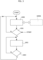
Figure 3 is a flow-chart exemplary of possible operation of embodiments according toFigure 2 , and -
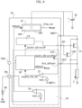
Figure 4 is a block diagram exemplary of a second possible option in implementing embodiments of the present description. - In the ensuing description, one or more specific details are illustrated, aimed at providing an in-depth understanding of examples of embodiments of this description. The embodiments may be obtained without one or more of the specific details, or with other methods, components, materials, etc. In other cases, known structures, materials, or operations are not illustrated or described in detail so that certain aspects of embodiments will not be obscured.
- Reference to "an embodiment" or "one embodiment" in the framework of the present description is intended to indicate that a particular configuration, structure, or characteristic described in relation to the embodiment is comprised in at least one embodiment. Hence, phrases such as "in an embodiment" or "in one embodiment" that may be present in one or more points of the present description do not necessarily refer to one and the same embodiment.
- Moreover, particular conformations, structures, or characteristics may be combined in any adequate way in one or more embodiments.
- The headings/references used herein are provided merely for convenience and hence do not define the extent of protection or the scope of the embodiments.
- Also, throughout the figures, unless the context indicates otherwise, like parts or elements are indicated with like reference symbols, and a corresponding description will not be repeated for each and every figure for brevity.
- As discussed, electronic fuses are generally exemplary of devices where a current sunk in an ON state, albeit small, may end up by acting as a battery drainer during load quiescent states where the device cannot be switched to the OFF state in so far as a (small) current is still supplied to the load.
- Electronic fuses share with conventional mechanical fuses the basic role of protecting against overcurrents an electrical load coupled to a supply source (a battery voltage, in the case of automotive applications, for instance). Electronic fuses may however distinguish over conventional mechanical fuses (which, before possibly "burning", always draw a current from the supply source) due to their ability to be brought to a state where (at least notionally) no current is drawn from the supply source.
- For the sake of simplicity and ease of understanding, the embodiments illustrated herein will be discussed primarily in connection with possible application in an electronic fuse.
- It will be again recalled that the embodiments are not linked by way of necessity to that application: in fact, one or more embodiments may be applied, more generally, to those contexts where a low current absorption standby state and the capability of transitioning from such a low-consumption state to a full operating state quickly, with no appreciable discontinuities for the load and the system are desirable features.
- The functional block diagram of
Figure 1 is generally illustrative of asystem 100 which employs an "intelligent" current absorption management circuit (oftentimes referred to as an e-fuse or eFuse) 10. - A
system 100 as illustrated inFigure 1 is configured to controllably supply to an electrical load L energy drawn from a supply source SS. - In the (purely illustrative) representation of
Figure 1 , the supply source SS is provided by a battery as may be the case of asystem 100 equipping a vehicle V. - It will be appreciated that both the source SS and the load L may be distinct elements from the embodiments, and the
system 100 may be intended to be coupled to the supply source SS (at a node VBAT+) and to the load L (at a node OUT) only when the system is installed and configured for operation. - As illustrated in
Figure 1 , electrical supply of the load L is controlled via a (power)switch 12. A power MOS transistor (power MOSFET) may be exemplary of such a switch. - For simplicity and ease of explanation, the
switch 12 is represented inFigure 1 as an integral part of thesystem 100. Theswitch 12 may however be a distinct element from the embodiments. - As otherwise conventional in the art, a
system 100 as illustrated in the functional block diagram ofFigure 1 may include a wide palette of functionalities. - As illustrated in
Figure 1 , these functionalities may be arranged in: - a first section I, which includes system and safety-related functions co-operating with an I/O interface (on the left-hand side of
Figure 1 ) such as, for instance, parameter setting 101, self-test 102, diagnostic 103,control 104,watchdog 105 and limp-home 106 functionalities; - a second section II, which includes power MOSFET protections such as, for instance, back electro-motive force (BEMF) clamping 107 and
thermal protection 108 functionalities; and - a third section III, which includes power MOSFET gate driver and sensor functionalities such as, for instance,
output voltage sensing 109,charge pump 110,junction temperature sensing 111, supply voltage (VBAT+) sensing 112 andcurrent sensing 113 functionalities. - In general terms, and unless indicated otherwise in the following, system architecture as exemplified in
Figure 1 can be regarded as conventional in the art, which makes it unnecessary to provide a more detailed description. - Embodiments as exemplified herein are primarily concerned with possible interplay of the
functionality 10 with the other functionalities in the architecture, for instance with thepower switch 12 and thecurrent sensing functionality 113. - This may occur, for instance, via standby monitoring and standby switch functionalities as generally represented by
blocks Figure 1 and suited to be implemented as exemplified inFigures 2 and3 . - For that reason, various possible implementation options of the functional architecture of
Figure 1 will now be discussed by placing emphasis on co-operation of thefunctionality 10 with the other functionalities in the architecture with thepower switch 12. - To that effect, the
power switch 12 is shown having a current path therethrough (source-drain in the case of a field-effect transistor such as a MOSFET transistor) coupled between the supply source SS (at a node VBAT+) and the load L (at a node OUT). - As noted, the load L can be notionally any kind of electrical load; the embodiments are thus largely "transparent" to the nature and characteristics of the load L.
- By way of general reference, two types of implementation options will be discussed in connection with
Figures 2 to 4 as exemplary of possible variants where: - the
power switch 12 may be external to (and thus distinct from) thecircuit 10, in contrast to the representation ofFigure 1 , where theswitch 12 is included in thecircuit 10, and/or - the
circuit 10 can switch to a low-current consumption state (ON standby state) where a small current is delivered to the load, either in response to a command from an external controller (a microcontroller or pC, for instance, as discussed in connection withFigure 2 ) or as a result of automatic enablement of that state in the absence of an external command (as discussed in connection withFigure 4 ). - As noted, for the sake of simplicity and ease of explanation, unless indicated otherwise, throughout the figures like parts or elements are indicated with like reference symbols and a corresponding description will not be repeated for each and every figure for brevity.
- Also, features and details discussed in connection with one implementation option can be applied, singly or in combination, in another implementation option. That is, a feature or detail being here illustrated, singly or in combination, within the framework of one implementation option shall not be construed as an indication that such a feature or detail can be used exclusively in the implementation option where the features or detail is illustrated herein.
- In
Figure 2 , a currentabsorption management circuit 10 is illustrated coupled to a supply source SS (at a node VBAT+) and to a load L (at a node OUT) in order to control current supply to the load L via apower switch 12. - The current path through the power switch 12 (source-drain in the case of a field-effect transistor such as a MOSFET transistor) is thus coupled between the supply source SS and the load L, so that load energization, that is current flow through the load, is:
- facilitated (permitted) in response to the
switch 12 being turned ON, namely made conductive, and - countered (prevented) in response to the
switch 12 being turned OFF, namely made non-conductive. - The
power switch 12 can be alternatively switched on (that is, made conductive) and off (that is, made non-conductive) via a drive signal produced by adriver 14 and applied via a node GD to the control node (gate, in the case of a field-effect transistor such as a MOSFET transistor) of thepower switch 12. -
Reference 16 indicates a voltage regulator coupled to the supply source SS and configured (in a manner known per se to those of skill in the art) to provide a regulated supply voltage Vreg_out to the other parts of thedevice 100 as illustrated in the functional block diagram ofFigure 1 . - As discussed in the following, the voltage regulator may comprise a high-
power section 16A (LDO, for instance) and a low-power section 16B (a no-cap preregulator, for instance). -
Reference 18 denotes as a whole a part (subsystem) of thecircuit 10 devoted to managing a standby state of thecircuit 10 as discussed in the following. - This may occur in response to a standby signal received at an input node OSS from a controller MC (a microcontroller or µC, for instance). As illustrated, the controller MC may be an external controller, distinct from the
circuit 10. - As illustrated in
Figure 2 , thesubsystem 18 comprises activestandby logic circuitry 20 sensitive to a signal received at the node OSS from the controller MC as well as to a wake-up signal bypass_vds_sat from acomparator 22 which compares with a reference (voltage) threshold Vref_1 a signal which indicates the intensity of the current flowing into the load L at the node OUT and which, as discussed in the following, can be used to facilitate (quick) re-activation of themain switch 12 to a conductive state. - Such a re-activation signal may be obtained (in a manner known per se to those of skill in the art) via a current sensing functionality such as 113 in
Figure 1 . - As illustrated herein, such a re-activation signal may be simply obtained as a result of a feedback action based on the value of the voltage at the node OUT compared in a
comparator 22 with a (possibly adjustable) threshold Vref_1 referred to the supply voltage VBAT+. - The voltage at the node OUT (and thus the voltage drop between the voltage at the node VBAT+ and the voltage at the node OUT) can be reasonably assumed to be a function of the output current. In fact, an electronic switch in a conductive state can be regarded as a resistor having a resistance value, such as RDSon in the case of a field-effect transistor such as a MOSFET transistor.
- Consequently, a signal adapted to be supplied to the
comparator 22 for comparison with the threshold Vref_1 can be simply obtained by monitoring the voltage at the node OUT. - In one or more embodiments, a
secondary bypass switch 12A such as a (low-power) MOSFET transistor (p-channel for instance) may be coupled across the nodes VBAT+ and OUT thus having the current path therethrough (source-drain in the case of a field-effect transistor such as a MOSFET transistor) coupled between the supply source SS and the load L. - Stated otherwise, the re-activation signal may be simply obtained as a result of a feedback action based on the value of the voltage at the node OUT, that is by monitoring the (source-drain) voltage drop across the
secondary bypass switch 12A. - As illustrated in
Figure 2 thelogic circuitry 20 is configured to produce: - a first signal Switch_GD-on/off which is applied (via the driver circuit 14) to the control node (gate, in the case of a field-effect transistor such as a MOSFET transistor) of the
power switch 12 to turn it alternatively on (conductive) and off (non-conductive), - a second signal Switch_BS-on/off which is applied to the control node (gate, in the case of a field-effect transistor such as a MOSFET transistor) of the
secondary switch 12A to turn it alternatively on (conductive) and off (non-conductive), - a third signal stdbyon which is distributed to the other parts of the
device 100 as illustrated in the functional block diagram ofFigure 1 (supply of the signal stdbyon to thevoltage regulator 16 is explicitly represented in the upper portion ofFigure 2 ). - A possible sequence of operation of the
circuit 10 may contemplate an ON active-standby state. - This may be in addition to the conventional ON and OFF states of an electronic fuse, that is:
- an ON state (see also block 1000 in the flow-chart of
Figure 3 , discussed in the following), during which the load L (fully) energized with the load L coupled to the supply source SS through theswitch 12 made conductive (with theswitch 12A non-conductive), and - an OFF state (see also block 1000A in the flow-chart of
Figure 3 ), during which theswitch 12 de-couples the load L from the supply source SS as a result of the switch 12 (as well as theswitch 12A) being made non-conductive; such an OFF state may be entered into in response to an overcurrent event as detected at 113 inFigure 1 , for instance. - Operation of a
device 100 as illustrated inFigure 1 in those two ON and OFF states (seeblocks Figure 3 ) is conventional in the art, which makes it unnecessary to provide a more detailed description herein. - Also, it will be again recalled that application to an electronic fuse is considered herein merely by way of non-limiting example.
- The embodiments are not linked by way of necessity to being applied in electronic fuses in so far as an ON active-standby state may be advantageous in various devices where it is desired that a small current may still flow to a load such as L while the overall current consumption of the
circuit 10 is very low (less than 50µA, for instance, thus improving battery lifetime). - The capability of switching to a (full) ON state with the
power switch 12 turned quickly on (within 50-100µs since a normal load current is requested, for instance) is likewise desirable. - Operation of an implementation option as illustrated in
Figure 2 is exemplified in the flow-chart ofFigure 3 assuming that after START thecircuit 10 is in the (full) ON state as exemplified byblock 1000. - As noted, the
switch 12 may be turned off (made non-conductive -OFF state 1000A) in order to de-couple the load L from the supply source SS in response to an overcurrent event in eFuse operation. As noted, this is conventional in the art (which makes it unnecessary to provide a more detailed description herein) and likewise not mandatory for the embodiments. - Switching to the low-power-consumption ON active-standby state may be prompted by the occurrence of a triggering action as exemplified at STDBY.
- This may be indicated by a positive outcome Y of a check at
block 1001; in the presence of a negative outcome N the circuit simply loops back upstream thus maintaining the (full) ON state. - The triggering action exemplified at STDBY may involve the input node OSS being asserted (brought high, for instance) for a minimum time by the controller MC, while the
circuit 10 is in the ON state, with theswitch 12 conductive and the load L energized by the supply source SS. - The input node OSS being asserted may be recognized by the
device 10 as a command to enable the ON active-standby state. This command may be validated, for instance, as a result of the input node OSS being pulled-down, that is, brought to a low level. - In response to entering the ON active-standby state (as exemplified by
block 1002 inFigure 3 ), thelogic circuitry 20 may: - on the one hand, disable the
main switch 12 via the driver 14 (signal Switch_GD-on/off indicating an off condition desired where the supply source SS is no longer coupled to the load L via the switch 12), and - on the other hand, enable the
secondary switch 12A to maintain a reduced current supply (350mA-500mA, for instance) to the load L. - During the ON active-standby state, if the current supplied to the load L exceeds a threshold Iout_stdbyon (500mA @ VBAT+=13V, T=25°C, for instance) - which corresponds to a positive outcome Y of a check exemplified by
block 1003 inFigure 3 - thelogic circuitry 20 may switch back to the (full) ON state by: - on the one hand, re-enabling the
main switch 12 via the driver 14 (signal Switch_GD-on/off indicating an on condition desired), which can occur very rapidly; - on the other hand, disabling the
secondary switch 12A. - In the presence of a negative outcome N of the check represented by
block 1003, the circuit simply loops back upstream thus maintaining the ON active-standby state. - The related information on the intensity of the current supplied to the load L can be provided to the
logic circuitry 20 via thecomparator 22 in response to the comparison therein indicating that intensity of the current through the load L (indicated, for instance, by the re-activation signal which - as discussed in the foregoing - can be obtained as a result of a feedback action based on the voltage at the node OUT) has increased up to an intensity threshold as represented by Vref_1. - For instance, the
circuit 10 can be configured so that if, during the ON active-standby state with, e.g., Iout<350mA any pin (with possible exceptions as represented, for instance, by the OSS node) is pulled up, thedevice 100 will go back to the (full) ON state, re-activating thepower switch 12 and de-activating thesecondary switch 12A. - Of course, the quantitative figures given herein are merely exemplary and non-limiting of the embodiments.
- The signal stdbyon (which is indicative of the ON active-standby state being enabled and is distributed by the logic circuitry to the other parts of the device 100) can be exploited in the
voltage regulator 16 to selectively enable: - the high-power (and higher consumption)
regulator 16A, such as a low dropout (LDO) regulator, during the (full) ON state with thepower switch 12 turned on and thesecondary switch 12A turned off; or - a low-power (and low-consumption)
voltage preregulator 16B, during the ON active-standby state with thepower switch 12 turned off and thesecondary switch 12A turned on. - More generally, as represented in
Figure 2 by the signal stdbyon from thelogic circuitry 20 distributed to the various other functionalities in thearchitecture 100 ofFigure 1 , a current absorption management circuit as illustrated herein facilitates switching to a low-consumption state (notionally turning-off) these functionalities, thus dramatically reducing energy absorption. - This advantageously facilitates further reducing energy absorption from the supply source SS during the ON active-standby state.
- Also, waking-up from such a low-consumption state to a full operating state may take place quickly, with no appreciable discontinuities for the load L and the system as a whole.
- In
Figure 4 , unless the context indicates otherwise, parts or elements like parts or elements already discussed in connection with the previous figures are indicated with like reference symbols, so that a corresponding description will not be repeated for brevity. -
Figure 4 is exemplary of an implementation where the triggering action as exemplified at STDBY in the flowchart ofFigure 3 may result from a sensing action of the current through the load L with a command provided by an external controller MC no longer involved. - In a
circuit 10 as illustrated inFigure 4 , asensing transistor 12B (a MOSFET transistor, for instance) is provided having the current path therethrough (source-drain in the case of a field-effect transistor such as a MOSFET transistor, for instance) coupled across the nodes VBAT+ and OUT and the control node (gate, in the case of a field-effect transistor such as a MOSFET transistor, for instance) coupled to the control node GD (again gate, in the case of a field-effect transistor such as a MOSFET transistor) of thepower switch 12. - The current (feedback) path through the
sensing transistor 12B is also coupled to a (multi)sensing node MS configured to be coupled to ground GND, optionally via an (e.g., external) sensing resistor SR. -
Reference 24 denotes inFigure 4 a further comparator which compares the (e.g., voltage) signal at the node MS with a further (possibly adjustable) threshold Vref_2 referenced to ground. The output signal from thecomparator 24 is applied to thelogic circuitry 20. - During the (full) ON state, a device as illustrated in
Figure 4 will be able to detect (via the feedbackcurrent sensing network 12B, SR which supplies thecomparator 24 with the signal compared with the threshold Vref_2) a condition where the current through themain switch 12, and thus through the load L, has decreased reaching a lower threshold value as defined by Vref_2 (250mA @ VBAT= +13V, T=25°C, for instance). - Optionally, the
sensing network 12B, SR may be configured to operate with a very low current density and the resistance SR can be accordingly chosen (a resistance value of 420KOhm was found to be a sensible choice) to generate Vms=4,15V @Iout=250mA. - Here again, these quantitative figures are merely exemplary and non-limiting of the embodiments.
- When such detection occurs (see STDBY in
Figure 3 ), the circuit will automatically enter the ON active stand-by state as represented byblock 1002 in the flow-chart ofFigure 3 after a fixed time (about 150µs, for instance). - Here again, during the ON active-standby state, if the current supplied to the load L exceeds a threshold Iout_stdbyon (500mA @ VBAT+=13V, T=25°C, for instance) as indicated by a positive outcome Y of the check represented by
block 1003, thelogic circuitry 20 may switch back to the (full) ON state. In the presence of a negative outcome N of the check represented byblock 1003, the circuit simply loops back upstream thus maintaining the ON active-standby state. - In the case exemplified in
Figure 4 , the related information on the intensity of the current supplied to the load L can be provided to thelogic circuitry 20 via thecomparator 22 as discussed previously in connection withFigure 2 , namely as a result of a feedback action based on the voltage at the node OUT. - Here again, the
circuit 10 can be configured so that if, during the ON active-standby state with, e.g., Iout<350mA, any pin (with possible exceptions as represented, for instance, by the OSS node) is pulled up, thedevice 100 will go back to the (full) ON state, re-activating thepower switch 12 and de-activating thesecondary switch 12A. - Once more, the signal stdbyon which is indicative of the ON active-standby state being enabled and is distributed by the logic circuitry to the other parts of the
device 100 may be exploited in thevoltage regulator 16 to selectively enable: - a high-power (and higher consumption)
regulator 16A, such as a low dropout (LDO) regulator, activatable during the (full) ON state with thepower switch 12 turned on and thesecondary switch 12A turned off; or - a low-power (and low-consumption)
voltage preregulator 16B, activatable during the ON active-standby state with thepower switch 12 turned off and thesecondary switch 12A turned on. - More generally, as represented also in
Figure 4 by the signal stdbyon from thelogic circuitry 20 distributed to the various other functionalities in thearchitecture 100 ofFigure 1 , a current absorption management circuit as illustrated herein facilitates switching to a low- consumption state (notionally turning-off) these functionalities, thus dramatically reducing energy absorption. - This advantageously facilitates further reducing energy absorption from the supply source SS during the ON active-standby state.
- Also, waking-up from such a low-consumption state to a full operating state may take place quickly, with no appreciable discontinuities for the load L and the system as a whole.
- Briefly, a circuit as exemplified herein (for instance, 10) comprises:
- a first node (for instance, VBAT+) and a second node (for instance, OUT) configured to be coupled (respectively) to an electrical supply source (for instance, SS) and to an electrical load (for instance, L) configured to be supplied by the electrical supply source (for instance, SS) via an electronic switch (for instance, 12) having a control node,
- a third node (for instance, GD) configured to be coupled to the control node of the electronic switch to switch the electronic switch between a conductive state (for instance, 1000), wherein the electrical load is coupled to the supply source via the electronic switch, and a non-conductive state (for instance, 1000A, wherein the electrical load may not be coupled to the supply source via the electronic switch).
- A circuit as exemplified herein (further) comprises:
- a secondary electronic switch (for instance, 12A) intermediate the first node and the second node,
- control logic circuitry (for instance, 20) coupled to said third node and said secondary electronic switch to provide a first switch control signal (for instance, Switch_GD-on/off) applied (for instance, via 14) to said third node and a second switch control signal (for instance, Switch_BS-on/off) to the secondary electronic switch, the control logic circuitry (20) configured to provide the first switch control signal and the second switch control signal, alternately:
- in a first mode of operation (for instance, 1000), wherein the first switch control signal drives the electronic switch to the conductive state and the second switch control signal drives the secondary electronic switch to a non-conductive state, and
- in a second mode of operation (for instance, 1002), wherein the first switch control signal drives the electronic switch to the non-conductive state and the second switch control signal drives the secondary electronic switch to a conductive state, wherein the electrical load is coupled to the supply source via the secondary electronic switch.
- A circuit as exemplified herein comprises a fourth node (for instance, OSS) configured to receive a standby signal (for instance, MC), wherein the circuit control logic circuitry is configured to switch to said second mode of operation (from said first mode of operation, for instance) in response to said standby signal received (for instance, 1001) at said fourth node.
- A circuit as exemplified herein comprises current sensing circuitry (for instance, 12B, SR, 24) configured to sense the intensity of the current flowing through the electrical load, the current sensing circuitry coupled to the control logic circuitry, wherein the control logic circuitry is configured to switch from said first mode of operation to said second mode of operation in response to the current flowing through the electrical load dropping to a lower threshold (for instance, Vref_2).
- In a circuit as exemplified herein, the current sensing circuitry may comprise a sensing transistor (for instance, 12B) having a control node coupled to said third node and a current path therethrough included in a current feedback line from said first node (for instance, VBAT+) to a further node (for instance, MS) coupleable to ground, preferably via a resistor (for instance, SR).
- A circuit as exemplified herein comprises current sensing circuitry (for
instance - A circuit as exemplified herein may comprise supply regulator circuitry (for instance, 16) having a first supply regulator section (for instance, 16A) and a second supply regulator section (for instance, 16B), the second supply regulator section having lower energy absorption than the first supply regulator section, wherein the control logic circuitry is coupled (for instance, stdbyon) to said supply regulator circuitry and configured to enable the first supply regulator section during the first mode of operation and the second supply regulator section during the second mode of operation.
- In a circuit as exemplified herein, the secondary electronic switch (for instance, 12A) may comprise a low-power electronic switch.
- An electronic switch such a MOSFET transistor having a RDSon resistance (at full VGS) of about 10 Ohm may be exemplary of such a low-power switch.
- A circuit as exemplified herein may include said electronic switch having a control node (as assumed in
Figure 1 , for instance), and the secondary electronic switch may comprise a low-power electronic switch configured to be traversed during conduction by a current of lower intensity than the current traversing said electronic switch during conduction. - A system as exemplified herein (a power distribution system for use in the automotive sector, for instance) comprises:
- an electrical supply source (for instance, SS),
- an electrical load (for instance, L),
- an electronic switch (for instance, 12) having a control node to switch the electronic switch between a conductive state, wherein the electrical load is coupled to the supply source via the electronic switch, and a non-conductive state (wherein the electrical load is not coupled to the supply source via the electronic switch),
- a circuit (for instance, 10, with the
switch 12 being a distinct component from the circuit - as illustrated inFigures 2 and4 , or included in the circuit as assumed inFigure 1 ) as exemplified herein wherein the first node (for instance, VBAT+) is coupled to the electrical supply source (for instance, SS), the second node (for instance, OUT) is coupled to the electrical load (for instance, L) and the third node (for instance, GD) is coupled to the control node of the electronic switch (for instance, 12). - A system as exemplified herein may comprise energy absorbing circuitry (see, for instance, the functionalities I,II,III in the
system 100Figure 1 ) supplied by said supply source (for instance, SS), the energy absorbing circuitry settable to a low-energy absorption mode in response to the control logic circuitry (for instance, 20) in said circuit (for instance, 10) being actuated in said second mode of operation (forinstance 1002, with the signal stdbyon distributed to the functionalities I,II,III in thesystem 100 inFigure 1 ). - A method of operating a circuit or a system as exemplified herein comprises actuating the control logic circuitry (for instance, 20), alternately:
- in said first mode of operation (for instance, 1000), wherein the first switch control signal (for instance, Switch_GD-on/off) drives the electronic switch (for instance, 12) to the conductive state and the second switch control signal (for instance, Switch_BS-on/off) drives the secondary electronic switch (for instance, 12A) to a non-conductive state, and
- in said second mode of operation (for instance, 1002), wherein the first switch control signal (for instance, Switch_GD-on/off) drives the electronic switch (for instance, 12) to the non-conductive state and the second switch control signal (for instance, Switch_BS-on/off) drives the secondary electronic switch (for instance, 12A) to a conductive state, wherein the electrical load (for instance, L) is coupled to the supply source (for instance, SS) via the secondary electronic switch.
- Without prejudice to the underlying principles, the details and embodiments may vary, even significantly, with respect to what has been described by way of example only, without departing from the extent of protection.
- The extent of protection is determined by the annexed claims.
Claims (6)
- A circuit (10), comprising:a first node (VBAT+) and a second node (OUT) configured to be coupled, respectively, to an electrical supply source (SS) and to an electrical load (L) configured to be supplied by the electrical supply source (SS) via an electronic switch (12) having a control node,a third node (GD) configured to be coupled to the control node of the electronic switch (12) to switch the electronic switch (12) between a conductive state (1000), wherein the electrical load (L) is coupled to the supply source (SS) via the electronic switch (12), and a non-conductive state (1000A),a secondary electronic switch (12A) coupled to the first node (VBAT+) and the second node (OUT) and also configured to couple the electrical load (L) to the supply source (SS), wherein the secondary electronic switch (12A) is configured to be traversed during conduction by a current of lower intensity than the current traversing said electronic switch (12) during conduction,control logic circuitry (20) coupled to said third node (GD) and said secondary electronic switch (12A) to provide a first switch control signal (Switch_GD-on/off) applied (14) to said third node (GD) and a second switch control signal (Switch_BS-on/off) to the secondary electronic switch (12A), the control logic circuitry (20) configured to provide the first switch control signal (Switch_GD-on/off) and the second switch control signal (Switch_BS-on/off), alternately:in a first mode of operation (1000), wherein the first switch control signal (Switch_GD-on/off) is configured to drive the electronic switch (12) to the conductive state, wherein the electrical load (L) is coupled to the supply source (SS) via the electronic switch (12), and the second switch control signal (Switch_BS-on/off) is configured to drive the secondary electronic switch (12A) to a non-conductive state, andin a second mode of operation (1002), wherein the first switch control signal (Switch_GD-on/off) is configured to drive the electronic switch (12) to the non-conductive state and the second switch control signal (Switch_BS-on/off) is configured to drive the secondary electronic switch (12A) to a conductive state,wherein:the circuit (10) further comprises a fourth node (OSS) configured to receive a standby signal (MC), wherein the circuit control logic circuitry (20) is configured to switch to said second mode of operation (1002) in response to said standby signal received (1001) at said fourth node (OSS), andthe circuit (10) comprises current sensing circuitry (12B, SR, 24) configured to sense the intensity of the current flowing through the electrical load (L), the current sensing circuitry (12B, SR, 24) coupled to the control logic circuitry (20), wherein the control logic circuitry (20) is configured to:switch from said first mode of operation (1000) to said second mode of operation (1002) in response to the current flowing through the electrical load (L) dropping to a lower threshold (Vref_2),switch from said second mode of operation (1002) to said first mode of operation (1000) in response to the current flowing through the electrical load (L) increasing to an upper threshold (Vref_1).
- The circuit (10) of claim 1, wherein the current sensing circuitry (12B, SR, 24) comprises a sensing transistor (12B) having a control node coupled to said third node (GD) and a current path therethrough included in a current feedback line from said first node (VBAT+) to a further node (MS) coupleable to ground, preferably via a resistor (SR).
- The circuit (10) of any of the previous claims, comprising supply regulator circuitry (16) having a first supply regulator section (16A) and a second supply regulator section (16B), the second supply regulator section (16B) having lower energy absorption than the first supply regulator section (16A), wherein the control logic circuitry (20) is coupled (stdbyon) to said supply regulator circuitry (16) and configured to enable the first supply regulator section (16A) during the first mode of operation (1000) and the second supply regulator section (16B) during the second mode of operation (1000).
- A system (100), comprising:an electrical supply source (SS),an electrical load (L),an electronic switch (12) having a control node to switch the electronic switch (12) between a conductive state (1000), wherein the electrical load (L) is coupled to the supply source (SS) via the electronic switch (12), and a non-conductive state (1000A),a circuit (10) according to any of claims 1 to 3,wherein said first node (VBAT+) is coupled to the electrical supply source (SS), the second node (OUT) is coupled to the electrical load (L) and the third node (GD) coupled to the control node of the electronic switch (12).
- The system (100) of claim 4, wherein the system comprises energy absorbing circuitry (I, II, III) supplied by said supply source (SS), the energy absorbing circuitry (I, II, III) settable to a low energy absorption mode in response (stdbyon) to the control logic circuitry (20) in said circuit (10) being actuated in said second mode of operation (1002).
- A method of operating a circuit according to any of claims 1 to 3 or a system according to any of claims 4 or 5, wherein the method comprises actuating the control logic circuitry (20), alternately:in said first mode of operation (1000), wherein the first switch control signal (Switch_GD-on/off) drives the electronic switch (12) to the conductive state, wherein the electrical load (L) is coupled to the supply source (SS) via the electronic switch (12), and the second switch control signal (Switch_BS-on/off) drives the secondary electronic switch (12A) to a non-conductive state, andin said second mode of operation (1002), wherein the first switch control signal (Switch_GD-on/off) drives the electronic switch (12) to the non-conductive state and the second switch control signal (Switch_BS-on/off) drives the secondary electronic switch (12A) to a conductive state, wherein the electrical load (L) is coupled to the supply source (SS) via the secondary electronic switch (12A),wherein the control logic circuitry (20) switches to said second mode of operation (1002) in response to the standby signal being received at said fourth node (OSS), or in response to detecting that the current flowing through the electrical load (L) having dropping to the lower threshold (Vref_2),and the control logic circuitry (20) switches to said first mode of operation (1000) in response to the current flowing through the electrical load (L) increasing to an upper threshold (Vref_1).
Applications Claiming Priority (1)
| Application Number | Priority Date | Filing Date | Title |
|---|---|---|---|
| IT202000030575 | 2020-12-11 |
Publications (2)
| Publication Number | Publication Date |
|---|---|
| EP4012866A1 EP4012866A1 (en) | 2022-06-15 |
| EP4012866B1 true EP4012866B1 (en) | 2023-12-27 |
Family
ID=74669450
Family Applications (1)
| Application Number | Title | Priority Date | Filing Date |
|---|---|---|---|
| EP21210682.7A Active EP4012866B1 (en) | 2020-12-11 | 2021-11-26 | Current absorption management circuit, corresponding system and method |
Country Status (2)
| Country | Link |
|---|---|
| US (1) | US11764773B2 (en) |
| EP (1) | EP4012866B1 (en) |
Families Citing this family (5)
| Publication number | Priority date | Publication date | Assignee | Title |
|---|---|---|---|---|
| IT201900002297A1 (en) | 2019-02-18 | 2020-08-18 | St Microelectronics Srl | PROTECTION CIRCUIT, SYSTEM AND CORRESPONDING PROCEDURE |
| EP3961229B1 (en) | 2020-08-25 | 2024-02-28 | STMicroelectronics S.r.l. | Electronic device and corresponding self-test method |
| US12394971B2 (en) | 2021-12-13 | 2025-08-19 | Stmicroelectronics S.R.L. | Electronic fuse systems and devices |
| US12506473B2 (en) | 2021-12-13 | 2025-12-23 | Stmicroelectronics S.R.L. | Electronic device |
| DE102024206319A1 (en) * | 2024-07-04 | 2026-01-08 | Robert Bosch Gesellschaft mit beschränkter Haftung | Power supply unit and a power supply system |
Family Cites Families (5)
| Publication number | Priority date | Publication date | Assignee | Title |
|---|---|---|---|---|
| US5030844A (en) * | 1990-06-25 | 1991-07-09 | Motorola, Inc. | DC power switch with inrush prevention |
| JP2001298861A (en) * | 2000-04-11 | 2001-10-26 | Asahi Optical Co Ltd | Power supply circuit and electronic still camera |
| US7760479B2 (en) * | 2008-04-09 | 2010-07-20 | Fairchild Semiconductor Corporation | Technique for combining in-rush current limiting and short circuit current limiting |
| US10008846B2 (en) * | 2015-10-20 | 2018-06-26 | Nxp B.V. | Control device for an electronic fuse and method for controlling an electronic fuse |
| DE102021111027A1 (en) * | 2021-04-29 | 2022-11-03 | Continental Automotive Gmbh | Vehicle electrical system, especially for a motor vehicle |
-
2021
- 2021-11-26 EP EP21210682.7A patent/EP4012866B1/en active Active
- 2021-12-08 US US17/545,719 patent/US11764773B2/en active Active
Also Published As
| Publication number | Publication date |
|---|---|
| US11764773B2 (en) | 2023-09-19 |
| US20220190816A1 (en) | 2022-06-16 |
| EP4012866A1 (en) | 2022-06-15 |
Similar Documents
| Publication | Publication Date | Title |
|---|---|---|
| US11764773B2 (en) | Current absorption management circuit, corresponding system and method | |
| US12394971B2 (en) | Electronic fuse systems and devices | |
| US7408755B1 (en) | Advanced inrush/transient current limit and overload/short circuit protection method and apparatus for DC voltage power supply | |
| US7345383B2 (en) | Abnormality detection apparatus for a power feed circuit | |
| US20090052096A1 (en) | Power Supply Controller | |
| US20230411947A1 (en) | Intelligent semiconductor switch | |
| US9627962B2 (en) | Fast blocking switch | |
| US20250044370A1 (en) | Power supply control device and failure detection method | |
| US10069493B2 (en) | Circuitry and method for operating an electronic switch | |
| KR100468018B1 (en) | Charge / discharge control circuit | |
| JP2012244658A (en) | On-board electronic control device | |
| US8035943B2 (en) | Protection circuit apparatus | |
| CN112448363B (en) | Electrical safety system providing over-current protection of electrical circuits in a vehicle | |
| US20180370464A1 (en) | Power supply control device | |
| CN118435069A (en) | Circuit arrangement for checking the switching capacity of electronic switches | |
| US9397652B2 (en) | Circuitry and method for operating such circuitry | |
| CN114629082B (en) | Current sink management circuit, corresponding system and method | |
| US20070035183A1 (en) | Power supply circuit | |
| CN218633340U (en) | Vehicle distribution circuit and vehicle electric power system | |
| US11563430B2 (en) | Transistor diagnostic circuit | |
| CN112068614A (en) | Temperature control heat dissipation circuit and electronic equipment | |
| US12179617B2 (en) | Quick turn off of contactor system during power off | |
| CN223472248U (en) | Intelligent electronic switch, integrated circuit chip, chip product and automobile | |
| US20240396325A1 (en) | Disable circuit for a current inrush limiter | |
| CN223322062U (en) | Intelligent electronic switches, integrated circuit chips, chip products and automobiles |
Legal Events
| Date | Code | Title | Description |
|---|---|---|---|
| PUAI | Public reference made under article 153(3) epc to a published international application that has entered the european phase |
Free format text: ORIGINAL CODE: 0009012 |
|
| STAA | Information on the status of an ep patent application or granted ep patent |
Free format text: STATUS: THE APPLICATION HAS BEEN PUBLISHED |
|
| AK | Designated contracting states |
Kind code of ref document: A1 Designated state(s): AL AT BE BG CH CY CZ DE DK EE ES FI FR GB GR HR HU IE IS IT LI LT LU LV MC MK MT NL NO PL PT RO RS SE SI SK SM TR |
|
| STAA | Information on the status of an ep patent application or granted ep patent |
Free format text: STATUS: REQUEST FOR EXAMINATION WAS MADE |
|
| 17P | Request for examination filed |
Effective date: 20220830 |
|
| RBV | Designated contracting states (corrected) |
Designated state(s): AL AT BE BG CH CY CZ DE DK EE ES FI FR GB GR HR HU IE IS IT LI LT LU LV MC MK MT NL NO PL PT RO RS SE SI SK SM TR |
|
| GRAP | Despatch of communication of intention to grant a patent |
Free format text: ORIGINAL CODE: EPIDOSNIGR1 |
|
| STAA | Information on the status of an ep patent application or granted ep patent |
Free format text: STATUS: GRANT OF PATENT IS INTENDED |
|
| INTG | Intention to grant announced |
Effective date: 20230712 |
|
| GRAS | Grant fee paid |
Free format text: ORIGINAL CODE: EPIDOSNIGR3 |
|
| GRAA | (expected) grant |
Free format text: ORIGINAL CODE: 0009210 |
|
| STAA | Information on the status of an ep patent application or granted ep patent |
Free format text: STATUS: THE PATENT HAS BEEN GRANTED |
|
| AK | Designated contracting states |
Kind code of ref document: B1 Designated state(s): AL AT BE BG CH CY CZ DE DK EE ES FI FR GB GR HR HU IE IS IT LI LT LU LV MC MK MT NL NO PL PT RO RS SE SI SK SM TR |
|
| REG | Reference to a national code |
Ref country code: GB Ref legal event code: FG4D |
|
| REG | Reference to a national code |
Ref country code: CH Ref legal event code: EP |
|
| REG | Reference to a national code |
Ref country code: DE Ref legal event code: R096 Ref document number: 602021008084 Country of ref document: DE |
|
| REG | Reference to a national code |
Ref country code: IE Ref legal event code: FG4D |
|
| PG25 | Lapsed in a contracting state [announced via postgrant information from national office to epo] |
Ref country code: GR Free format text: LAPSE BECAUSE OF FAILURE TO SUBMIT A TRANSLATION OF THE DESCRIPTION OR TO PAY THE FEE WITHIN THE PRESCRIBED TIME-LIMIT Effective date: 20240328 |
|
| REG | Reference to a national code |
Ref country code: LT Ref legal event code: MG9D |
|
| PG25 | Lapsed in a contracting state [announced via postgrant information from national office to epo] |
Ref country code: LT Free format text: LAPSE BECAUSE OF FAILURE TO SUBMIT A TRANSLATION OF THE DESCRIPTION OR TO PAY THE FEE WITHIN THE PRESCRIBED TIME-LIMIT Effective date: 20231227 |
|
| PG25 | Lapsed in a contracting state [announced via postgrant information from national office to epo] |
Ref country code: ES Free format text: LAPSE BECAUSE OF FAILURE TO SUBMIT A TRANSLATION OF THE DESCRIPTION OR TO PAY THE FEE WITHIN THE PRESCRIBED TIME-LIMIT Effective date: 20231227 |
|
| PG25 | Lapsed in a contracting state [announced via postgrant information from national office to epo] |
Ref country code: LT Free format text: LAPSE BECAUSE OF FAILURE TO SUBMIT A TRANSLATION OF THE DESCRIPTION OR TO PAY THE FEE WITHIN THE PRESCRIBED TIME-LIMIT Effective date: 20231227 Ref country code: GR Free format text: LAPSE BECAUSE OF FAILURE TO SUBMIT A TRANSLATION OF THE DESCRIPTION OR TO PAY THE FEE WITHIN THE PRESCRIBED TIME-LIMIT Effective date: 20240328 Ref country code: FI Free format text: LAPSE BECAUSE OF FAILURE TO SUBMIT A TRANSLATION OF THE DESCRIPTION OR TO PAY THE FEE WITHIN THE PRESCRIBED TIME-LIMIT Effective date: 20231227 Ref country code: ES Free format text: LAPSE BECAUSE OF FAILURE TO SUBMIT A TRANSLATION OF THE DESCRIPTION OR TO PAY THE FEE WITHIN THE PRESCRIBED TIME-LIMIT Effective date: 20231227 Ref country code: BG Free format text: LAPSE BECAUSE OF FAILURE TO SUBMIT A TRANSLATION OF THE DESCRIPTION OR TO PAY THE FEE WITHIN THE PRESCRIBED TIME-LIMIT Effective date: 20240327 |
|
| REG | Reference to a national code |
Ref country code: NL Ref legal event code: MP Effective date: 20231227 |
|
| REG | Reference to a national code |
Ref country code: AT Ref legal event code: MK05 Ref document number: 1645438 Country of ref document: AT Kind code of ref document: T Effective date: 20231227 |
|
| PG25 | Lapsed in a contracting state [announced via postgrant information from national office to epo] |
Ref country code: NL Free format text: LAPSE BECAUSE OF FAILURE TO SUBMIT A TRANSLATION OF THE DESCRIPTION OR TO PAY THE FEE WITHIN THE PRESCRIBED TIME-LIMIT Effective date: 20231227 |
|
| PG25 | Lapsed in a contracting state [announced via postgrant information from national office to epo] |
Ref country code: SE Free format text: LAPSE BECAUSE OF FAILURE TO SUBMIT A TRANSLATION OF THE DESCRIPTION OR TO PAY THE FEE WITHIN THE PRESCRIBED TIME-LIMIT Effective date: 20231227 Ref country code: RS Free format text: LAPSE BECAUSE OF FAILURE TO SUBMIT A TRANSLATION OF THE DESCRIPTION OR TO PAY THE FEE WITHIN THE PRESCRIBED TIME-LIMIT Effective date: 20231227 Ref country code: NO Free format text: LAPSE BECAUSE OF FAILURE TO SUBMIT A TRANSLATION OF THE DESCRIPTION OR TO PAY THE FEE WITHIN THE PRESCRIBED TIME-LIMIT Effective date: 20240327 Ref country code: NL Free format text: LAPSE BECAUSE OF FAILURE TO SUBMIT A TRANSLATION OF THE DESCRIPTION OR TO PAY THE FEE WITHIN THE PRESCRIBED TIME-LIMIT Effective date: 20231227 Ref country code: LV Free format text: LAPSE BECAUSE OF FAILURE TO SUBMIT A TRANSLATION OF THE DESCRIPTION OR TO PAY THE FEE WITHIN THE PRESCRIBED TIME-LIMIT Effective date: 20231227 |
|
| PG25 | Lapsed in a contracting state [announced via postgrant information from national office to epo] |
Ref country code: IS Free format text: LAPSE BECAUSE OF FAILURE TO SUBMIT A TRANSLATION OF THE DESCRIPTION OR TO PAY THE FEE WITHIN THE PRESCRIBED TIME-LIMIT Effective date: 20240427 |
|
| PG25 | Lapsed in a contracting state [announced via postgrant information from national office to epo] |
Ref country code: CZ Free format text: LAPSE BECAUSE OF FAILURE TO SUBMIT A TRANSLATION OF THE DESCRIPTION OR TO PAY THE FEE WITHIN THE PRESCRIBED TIME-LIMIT Effective date: 20231227 Ref country code: AT Free format text: LAPSE BECAUSE OF FAILURE TO SUBMIT A TRANSLATION OF THE DESCRIPTION OR TO PAY THE FEE WITHIN THE PRESCRIBED TIME-LIMIT Effective date: 20231227 |
|
| PG25 | Lapsed in a contracting state [announced via postgrant information from national office to epo] |
Ref country code: SK Free format text: LAPSE BECAUSE OF FAILURE TO SUBMIT A TRANSLATION OF THE DESCRIPTION OR TO PAY THE FEE WITHIN THE PRESCRIBED TIME-LIMIT Effective date: 20231227 |
|
| PG25 | Lapsed in a contracting state [announced via postgrant information from national office to epo] |
Ref country code: SM Free format text: LAPSE BECAUSE OF FAILURE TO SUBMIT A TRANSLATION OF THE DESCRIPTION OR TO PAY THE FEE WITHIN THE PRESCRIBED TIME-LIMIT Effective date: 20231227 Ref country code: SK Free format text: LAPSE BECAUSE OF FAILURE TO SUBMIT A TRANSLATION OF THE DESCRIPTION OR TO PAY THE FEE WITHIN THE PRESCRIBED TIME-LIMIT Effective date: 20231227 Ref country code: RO Free format text: LAPSE BECAUSE OF FAILURE TO SUBMIT A TRANSLATION OF THE DESCRIPTION OR TO PAY THE FEE WITHIN THE PRESCRIBED TIME-LIMIT Effective date: 20231227 Ref country code: IT Free format text: LAPSE BECAUSE OF FAILURE TO SUBMIT A TRANSLATION OF THE DESCRIPTION OR TO PAY THE FEE WITHIN THE PRESCRIBED TIME-LIMIT Effective date: 20231227 Ref country code: IS Free format text: LAPSE BECAUSE OF FAILURE TO SUBMIT A TRANSLATION OF THE DESCRIPTION OR TO PAY THE FEE WITHIN THE PRESCRIBED TIME-LIMIT Effective date: 20240427 Ref country code: EE Free format text: LAPSE BECAUSE OF FAILURE TO SUBMIT A TRANSLATION OF THE DESCRIPTION OR TO PAY THE FEE WITHIN THE PRESCRIBED TIME-LIMIT Effective date: 20231227 Ref country code: CZ Free format text: LAPSE BECAUSE OF FAILURE TO SUBMIT A TRANSLATION OF THE DESCRIPTION OR TO PAY THE FEE WITHIN THE PRESCRIBED TIME-LIMIT Effective date: 20231227 Ref country code: AT Free format text: LAPSE BECAUSE OF FAILURE TO SUBMIT A TRANSLATION OF THE DESCRIPTION OR TO PAY THE FEE WITHIN THE PRESCRIBED TIME-LIMIT Effective date: 20231227 |
|
| PG25 | Lapsed in a contracting state [announced via postgrant information from national office to epo] |
Ref country code: PL Free format text: LAPSE BECAUSE OF FAILURE TO SUBMIT A TRANSLATION OF THE DESCRIPTION OR TO PAY THE FEE WITHIN THE PRESCRIBED TIME-LIMIT Effective date: 20231227 Ref country code: PT Free format text: LAPSE BECAUSE OF FAILURE TO SUBMIT A TRANSLATION OF THE DESCRIPTION OR TO PAY THE FEE WITHIN THE PRESCRIBED TIME-LIMIT Effective date: 20240429 |
|
| PG25 | Lapsed in a contracting state [announced via postgrant information from national office to epo] |
Ref country code: PT Free format text: LAPSE BECAUSE OF FAILURE TO SUBMIT A TRANSLATION OF THE DESCRIPTION OR TO PAY THE FEE WITHIN THE PRESCRIBED TIME-LIMIT Effective date: 20240429 Ref country code: PL Free format text: LAPSE BECAUSE OF FAILURE TO SUBMIT A TRANSLATION OF THE DESCRIPTION OR TO PAY THE FEE WITHIN THE PRESCRIBED TIME-LIMIT Effective date: 20231227 |
|
| REG | Reference to a national code |
Ref country code: DE Ref legal event code: R097 Ref document number: 602021008084 Country of ref document: DE |
|
| PG25 | Lapsed in a contracting state [announced via postgrant information from national office to epo] |
Ref country code: DK Free format text: LAPSE BECAUSE OF FAILURE TO SUBMIT A TRANSLATION OF THE DESCRIPTION OR TO PAY THE FEE WITHIN THE PRESCRIBED TIME-LIMIT Effective date: 20231227 |
|
| PG25 | Lapsed in a contracting state [announced via postgrant information from national office to epo] |
Ref country code: DK Free format text: LAPSE BECAUSE OF FAILURE TO SUBMIT A TRANSLATION OF THE DESCRIPTION OR TO PAY THE FEE WITHIN THE PRESCRIBED TIME-LIMIT Effective date: 20231227 |
|
| PLBE | No opposition filed within time limit |
Free format text: ORIGINAL CODE: 0009261 |
|
| STAA | Information on the status of an ep patent application or granted ep patent |
Free format text: STATUS: NO OPPOSITION FILED WITHIN TIME LIMIT |
|
| 26N | No opposition filed |
Effective date: 20240930 |
|
| PG25 | Lapsed in a contracting state [announced via postgrant information from national office to epo] |
Ref country code: SI Free format text: LAPSE BECAUSE OF FAILURE TO SUBMIT A TRANSLATION OF THE DESCRIPTION OR TO PAY THE FEE WITHIN THE PRESCRIBED TIME-LIMIT Effective date: 20231227 |
|
| REG | Reference to a national code |
Ref country code: CH Ref legal event code: PL |
|
| PG25 | Lapsed in a contracting state [announced via postgrant information from national office to epo] |
Ref country code: MC Free format text: LAPSE BECAUSE OF FAILURE TO SUBMIT A TRANSLATION OF THE DESCRIPTION OR TO PAY THE FEE WITHIN THE PRESCRIBED TIME-LIMIT Effective date: 20231227 |
|
| PG25 | Lapsed in a contracting state [announced via postgrant information from national office to epo] |
Ref country code: LU Free format text: LAPSE BECAUSE OF NON-PAYMENT OF DUE FEES Effective date: 20241126 |
|
| REG | Reference to a national code |
Ref country code: CH Ref legal event code: PL |
|
| PG25 | Lapsed in a contracting state [announced via postgrant information from national office to epo] |
Ref country code: CH Free format text: LAPSE BECAUSE OF NON-PAYMENT OF DUE FEES Effective date: 20241130 |
|
| REG | Reference to a national code |
Ref country code: BE Ref legal event code: MM Effective date: 20241130 |
|
| PG25 | Lapsed in a contracting state [announced via postgrant information from national office to epo] |
Ref country code: BE Free format text: LAPSE BECAUSE OF NON-PAYMENT OF DUE FEES Effective date: 20241130 |
|
| PG25 | Lapsed in a contracting state [announced via postgrant information from national office to epo] |
Ref country code: FR Free format text: LAPSE BECAUSE OF NON-PAYMENT OF DUE FEES Effective date: 20241130 |
|
| PG25 | Lapsed in a contracting state [announced via postgrant information from national office to epo] |
Ref country code: IE Free format text: LAPSE BECAUSE OF NON-PAYMENT OF DUE FEES Effective date: 20241126 |
|
| PGFP | Annual fee paid to national office [announced via postgrant information from national office to epo] |
Ref country code: DE Payment date: 20251022 Year of fee payment: 5 |
|
| PG25 | Lapsed in a contracting state [announced via postgrant information from national office to epo] |
Ref country code: HU Free format text: LAPSE BECAUSE OF FAILURE TO SUBMIT A TRANSLATION OF THE DESCRIPTION OR TO PAY THE FEE WITHIN THE PRESCRIBED TIME-LIMIT; INVALID AB INITIO Effective date: 20211126 |
|
| PG25 | Lapsed in a contracting state [announced via postgrant information from national office to epo] |
Ref country code: CY Free format text: LAPSE BECAUSE OF FAILURE TO SUBMIT A TRANSLATION OF THE DESCRIPTION OR TO PAY THE FEE WITHIN THE PRESCRIBED TIME-LIMIT; INVALID AB INITIO Effective date: 20211126 |
|
| PG25 | Lapsed in a contracting state [announced via postgrant information from national office to epo] |
Ref country code: HR Free format text: LAPSE BECAUSE OF FAILURE TO SUBMIT A TRANSLATION OF THE DESCRIPTION OR TO PAY THE FEE WITHIN THE PRESCRIBED TIME-LIMIT Effective date: 20231227 |