EP4012764A1 - Semiconductor device module and method of assembly - Google Patents
Semiconductor device module and method of assembly Download PDFInfo
- Publication number
- EP4012764A1 EP4012764A1 EP20213965.5A EP20213965A EP4012764A1 EP 4012764 A1 EP4012764 A1 EP 4012764A1 EP 20213965 A EP20213965 A EP 20213965A EP 4012764 A1 EP4012764 A1 EP 4012764A1
- Authority
- EP
- European Patent Office
- Prior art keywords
- semiconductor die
- die
- substrate
- semiconductor
- igbt
- Prior art date
- Legal status (The legal status is an assumption and is not a legal conclusion. Google has not performed a legal analysis and makes no representation as to the accuracy of the status listed.)
- Pending
Links
Images



Classifications
-
- H—ELECTRICITY
- H10—SEMICONDUCTOR DEVICES; ELECTRIC SOLID-STATE DEVICES NOT OTHERWISE PROVIDED FOR
- H10W—GENERIC PACKAGES, INTERCONNECTIONS, CONNECTORS OR OTHER CONSTRUCTIONAL DETAILS OF DEVICES COVERED BY CLASS H10
- H10W90/00—Package configurations
-
- H—ELECTRICITY
- H10—SEMICONDUCTOR DEVICES; ELECTRIC SOLID-STATE DEVICES NOT OTHERWISE PROVIDED FOR
- H10D—INORGANIC ELECTRIC SEMICONDUCTOR DEVICES
- H10D12/00—Bipolar devices controlled by the field effect, e.g. insulated-gate bipolar transistors [IGBT]
- H10D12/411—Insulated-gate bipolar transistors [IGBT]
-
- H—ELECTRICITY
- H10—SEMICONDUCTOR DEVICES; ELECTRIC SOLID-STATE DEVICES NOT OTHERWISE PROVIDED FOR
- H10D—INORGANIC ELECTRIC SEMICONDUCTOR DEVICES
- H10D8/00—Diodes
-
- H—ELECTRICITY
- H10—SEMICONDUCTOR DEVICES; ELECTRIC SOLID-STATE DEVICES NOT OTHERWISE PROVIDED FOR
- H10W—GENERIC PACKAGES, INTERCONNECTIONS, CONNECTORS OR OTHER CONSTRUCTIONAL DETAILS OF DEVICES COVERED BY CLASS H10
- H10W70/00—Package substrates; Interposers; Redistribution layers [RDL]
- H10W70/40—Leadframes
- H10W70/481—Leadframes for devices being provided for in groups H10D8/00 - H10D48/00
-
- H—ELECTRICITY
- H10—SEMICONDUCTOR DEVICES; ELECTRIC SOLID-STATE DEVICES NOT OTHERWISE PROVIDED FOR
- H10W—GENERIC PACKAGES, INTERCONNECTIONS, CONNECTORS OR OTHER CONSTRUCTIONAL DETAILS OF DEVICES COVERED BY CLASS H10
- H10W72/00—Interconnections or connectors in packages
- H10W72/071—Connecting or disconnecting
- H10W72/073—Connecting or disconnecting of die-attach connectors
-
- H—ELECTRICITY
- H10—SEMICONDUCTOR DEVICES; ELECTRIC SOLID-STATE DEVICES NOT OTHERWISE PROVIDED FOR
- H10W—GENERIC PACKAGES, INTERCONNECTIONS, CONNECTORS OR OTHER CONSTRUCTIONAL DETAILS OF DEVICES COVERED BY CLASS H10
- H10W76/00—Containers; Fillings or auxiliary members therefor; Seals
- H10W76/40—Fillings or auxiliary members in containers, e.g. centering rings
-
- H—ELECTRICITY
- H10—SEMICONDUCTOR DEVICES; ELECTRIC SOLID-STATE DEVICES NOT OTHERWISE PROVIDED FOR
- H10W—GENERIC PACKAGES, INTERCONNECTIONS, CONNECTORS OR OTHER CONSTRUCTIONAL DETAILS OF DEVICES COVERED BY CLASS H10
- H10W40/00—Arrangements for thermal protection or thermal control
- H10W40/20—Arrangements for cooling
- H10W40/25—Arrangements for cooling characterised by their materials
- H10W40/255—Arrangements for cooling characterised by their materials having a laminate or multilayered structure, e.g. direct bond copper [DBC] ceramic substrates
-
- H—ELECTRICITY
- H10—SEMICONDUCTOR DEVICES; ELECTRIC SOLID-STATE DEVICES NOT OTHERWISE PROVIDED FOR
- H10W—GENERIC PACKAGES, INTERCONNECTIONS, CONNECTORS OR OTHER CONSTRUCTIONAL DETAILS OF DEVICES COVERED BY CLASS H10
- H10W70/00—Package substrates; Interposers; Redistribution layers [RDL]
- H10W70/60—Insulating or insulated package substrates; Interposers; Redistribution layers
- H10W70/611—Insulating or insulated package substrates; Interposers; Redistribution layers for connecting multiple chips together
-
- H—ELECTRICITY
- H10—SEMICONDUCTOR DEVICES; ELECTRIC SOLID-STATE DEVICES NOT OTHERWISE PROVIDED FOR
- H10W—GENERIC PACKAGES, INTERCONNECTIONS, CONNECTORS OR OTHER CONSTRUCTIONAL DETAILS OF DEVICES COVERED BY CLASS H10
- H10W72/00—Interconnections or connectors in packages
- H10W72/071—Connecting or disconnecting
- H10W72/073—Connecting or disconnecting of die-attach connectors
- H10W72/07351—Connecting or disconnecting of die-attach connectors characterised by changes in properties of the die-attach connectors during connecting
- H10W72/07354—Connecting or disconnecting of die-attach connectors characterised by changes in properties of the die-attach connectors during connecting changes in dispositions
-
- H—ELECTRICITY
- H10—SEMICONDUCTOR DEVICES; ELECTRIC SOLID-STATE DEVICES NOT OTHERWISE PROVIDED FOR
- H10W—GENERIC PACKAGES, INTERCONNECTIONS, CONNECTORS OR OTHER CONSTRUCTIONAL DETAILS OF DEVICES COVERED BY CLASS H10
- H10W72/00—Interconnections or connectors in packages
- H10W72/30—Die-attach connectors
- H10W72/341—Dispositions of die-attach connectors, e.g. layouts
- H10W72/347—Dispositions of multiple die-attach connectors
-
- H—ELECTRICITY
- H10—SEMICONDUCTOR DEVICES; ELECTRIC SOLID-STATE DEVICES NOT OTHERWISE PROVIDED FOR
- H10W—GENERIC PACKAGES, INTERCONNECTIONS, CONNECTORS OR OTHER CONSTRUCTIONAL DETAILS OF DEVICES COVERED BY CLASS H10
- H10W72/00—Interconnections or connectors in packages
- H10W72/30—Die-attach connectors
- H10W72/351—Materials of die-attach connectors
- H10W72/352—Materials of die-attach connectors comprising metals or metalloids, e.g. solders
-
- H—ELECTRICITY
- H10—SEMICONDUCTOR DEVICES; ELECTRIC SOLID-STATE DEVICES NOT OTHERWISE PROVIDED FOR
- H10W—GENERIC PACKAGES, INTERCONNECTIONS, CONNECTORS OR OTHER CONSTRUCTIONAL DETAILS OF DEVICES COVERED BY CLASS H10
- H10W72/00—Interconnections or connectors in packages
- H10W72/851—Dispositions of multiple connectors or interconnections
- H10W72/874—On different surfaces
- H10W72/884—Die-attach connectors and bond wires
-
- H—ELECTRICITY
- H10—SEMICONDUCTOR DEVICES; ELECTRIC SOLID-STATE DEVICES NOT OTHERWISE PROVIDED FOR
- H10W—GENERIC PACKAGES, INTERCONNECTIONS, CONNECTORS OR OTHER CONSTRUCTIONAL DETAILS OF DEVICES COVERED BY CLASS H10
- H10W72/00—Interconnections or connectors in packages
- H10W72/90—Bond pads, in general
- H10W72/941—Dispositions of bond pads
- H10W72/944—Dispositions of multiple bond pads
-
- H—ELECTRICITY
- H10—SEMICONDUCTOR DEVICES; ELECTRIC SOLID-STATE DEVICES NOT OTHERWISE PROVIDED FOR
- H10W—GENERIC PACKAGES, INTERCONNECTIONS, CONNECTORS OR OTHER CONSTRUCTIONAL DETAILS OF DEVICES COVERED BY CLASS H10
- H10W90/00—Package configurations
- H10W90/401—Package configurations characterised by multiple insulating or insulated package substrates, interposers or RDLs
-
- H—ELECTRICITY
- H10—SEMICONDUCTOR DEVICES; ELECTRIC SOLID-STATE DEVICES NOT OTHERWISE PROVIDED FOR
- H10W—GENERIC PACKAGES, INTERCONNECTIONS, CONNECTORS OR OTHER CONSTRUCTIONAL DETAILS OF DEVICES COVERED BY CLASS H10
- H10W90/00—Package configurations
- H10W90/701—Package configurations characterised by the relative positions of pads or connectors relative to package parts
- H10W90/731—Package configurations characterised by the relative positions of pads or connectors relative to package parts of die-attach connectors
- H10W90/732—Package configurations characterised by the relative positions of pads or connectors relative to package parts of die-attach connectors between stacked chips
-
- H—ELECTRICITY
- H10—SEMICONDUCTOR DEVICES; ELECTRIC SOLID-STATE DEVICES NOT OTHERWISE PROVIDED FOR
- H10W—GENERIC PACKAGES, INTERCONNECTIONS, CONNECTORS OR OTHER CONSTRUCTIONAL DETAILS OF DEVICES COVERED BY CLASS H10
- H10W90/00—Package configurations
- H10W90/701—Package configurations characterised by the relative positions of pads or connectors relative to package parts
- H10W90/731—Package configurations characterised by the relative positions of pads or connectors relative to package parts of die-attach connectors
- H10W90/734—Package configurations characterised by the relative positions of pads or connectors relative to package parts of die-attach connectors between a chip and a stacked insulating package substrate, interposer or RDL
-
- H—ELECTRICITY
- H10—SEMICONDUCTOR DEVICES; ELECTRIC SOLID-STATE DEVICES NOT OTHERWISE PROVIDED FOR
- H10W—GENERIC PACKAGES, INTERCONNECTIONS, CONNECTORS OR OTHER CONSTRUCTIONAL DETAILS OF DEVICES COVERED BY CLASS H10
- H10W90/00—Package configurations
- H10W90/701—Package configurations characterised by the relative positions of pads or connectors relative to package parts
- H10W90/731—Package configurations characterised by the relative positions of pads or connectors relative to package parts of die-attach connectors
- H10W90/736—Package configurations characterised by the relative positions of pads or connectors relative to package parts of die-attach connectors between a chip and a stacked lead frame, conducting package substrate or heat sink
-
- H—ELECTRICITY
- H10—SEMICONDUCTOR DEVICES; ELECTRIC SOLID-STATE DEVICES NOT OTHERWISE PROVIDED FOR
- H10W—GENERIC PACKAGES, INTERCONNECTIONS, CONNECTORS OR OTHER CONSTRUCTIONAL DETAILS OF DEVICES COVERED BY CLASS H10
- H10W90/00—Package configurations
- H10W90/701—Package configurations characterised by the relative positions of pads or connectors relative to package parts
- H10W90/751—Package configurations characterised by the relative positions of pads or connectors relative to package parts of bond wires
- H10W90/753—Package configurations characterised by the relative positions of pads or connectors relative to package parts of bond wires between laterally-adjacent chips
Definitions
- Embodiments relate to the field of semiconductor devices, and in particular, packages for power semiconductor chips.
- fast switching power semiconductor devices normally employ fast switching diodes such as freewheeling diodes to protect the power semiconductor device from inductive loads, including motor coils or relay windings.
- fast switching diodes such as freewheeling diodes to protect the power semiconductor device from inductive loads, including motor coils or relay windings.
- the freewheel diode changes from a conducting state to a blocking state as it becomes reversed biased.
- the freewheeling diode becomes forward biased and the collapse of the energy stored, for example, in a coil, causes a current to flow through the freewheel diode. Without the protection of the freewheeling diode, a high di/dt current may occur, causing a high voltage spike or transient to flow, and possibly damaging the switching device.
- power semiconductor devices such as insulated gate bipolar transistors (IGBTs) are often arranged in power semiconductor modules, such as one or more substrates, such as 2, 4 or 6 substrates, similar to each other.
- Each substrate including wires and resistors, hold pairs of IGBT die (chips) and diode chips, where one or more IGBT chips may be paired with a diode chip.
- This arrangement provides a modular manner to switch currents of a desirable amount by choosing the appropriate number of chips. Because the IGBT chips and diode chips are arranged in a planar configuration on a substrate, the substrates need to be sized to accommodate all of the chips, including wiring between chips. As such, power semiconductor modules may be unduly large in size to accommodate the required number of substrates and power semiconductor devices.
- a semiconductor device module may include a first substrate; and a semiconductor die assembly, disposed on the first substrate.
- the semiconductor die assembly may include a first semiconductor die, bonded to the first substrate; a second semiconductor die, disposed over the first semiconductor die; and an electrical connector, disposed between the first semiconductor die and the second semiconductor die, wherein the semiconductor die assembly comprises an insulated gate bipolar transistor (IGBT) die and a freewheeling diode die.
- IGBT insulated gate bipolar transistor
- a method of forming a semiconductor device module may include providing a first substrate and affixing a semiconductor die assembly to the first substrate.
- the semiconductor die assembly may include a first semiconductor die, bonded to the first substrate; a second semiconductor die, disposed over the first semiconductor die; and an electrical connector, disposed between the first semiconductor die and the second semiconductor die, wherein the first semiconductor die assembly comprises an insulated gate bipolar transistor (IGBT) die and a freewheeling diode die.
- IGBT insulated gate bipolar transistor
- a semiconductor device module may include a first substrate; and a semiconductor die assembly, disposed on the first substrate, the semiconductor die assembly comprising a stacked configuration of a first insulated gate bipolar transistor (IGBT) die and a freewheeling diode die, and an electrical connector, disposed between the IGBT die and the freewheeling diode semiconductor die.
- IGBT insulated gate bipolar transistor
- the IGBT die may be directly bonded to the first substrate, wherein the stacked configuration defines a first die area, equivalent to an area of the IGBT die.
- the terms “on,” “overlying,” “disposed on” and “over” may be used in the following description and claims. “On,” “overlying,” “disposed on” and “over” may be used to indicate that two or more elements are in direct physical contact with one another. Also, the term “on,”, “overlying,” “disposed on,” and “over”, may mean that two or more elements are not in direct contact with one another. For example, “over” may mean that one element is above another element while not contacting one another and may have another element or elements in between the two elements.
- a semiconductor device module and techniques for assembly are provided for power semiconductor devices.
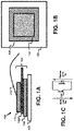
- FIG. 1A there is shown a side view of a semiconductor device module 100, according to various embodiments of the disclosure.
- FIG. 1B shows a top plan view of a variant of the semiconductor device module 100.
- FIG. 1C illustrates an electrical circuit representation of the semiconductor device module 100.
- the semiconductor device module 100 includes a first substrate 102, a semiconductor die assembly 104, disposed on the first substrate 102.
- the first substrate 102 may be a known material stack such as copper/aluminum oxide/copper also known as DCB or DBC, according to some embodiments.
- the first substrate may include an insulator body sandwiched between metallic layers, and may be referred to as an insulator substrate.
- the semiconductor die assembly 104 includes a first semiconductor die 106, attached to the first substrate 102, a second semiconductor die 110, disposed over the first semiconductor die 106, wire bonding 112, and an electrical connector 108, disposed between the first semiconductor die 106 and the second semiconductor die 110.
- the semiconductor die assembly 104 includes an insulated gate bipolar transistor (IGBT) die and a freewheeling diode die.
- IGBT insulated gate bipolar transistor
- the IGBT die may be disposed in contact with the first substrate 102.
- an IGBT die may be coupled with a diode die, used as a freewheeling diode to protect the IGBT die.
- the first semiconductor die 106 may be an IGBT die
- the second semiconductor die 110 may be a freewheeling diode die.
- the IGBT die, such as the first semiconductor die 106 is disposed over the first substrate 102 in a first region, and occupies a first area (in plan view, shown in FIG. 1B ), while the freewheeling diode die, such as second semiconductor die 110, occupies a second area, less than the first area.
- the second area may be on the order of 50% of the first area, such as 40%-60%.
- the second semiconductor die 110 completely overlaps the first semiconductor die 106 as shown in plan view of FIG. 1B .
- the semiconductor die assembly 104 is characterized by a stacked configuration of an IGBT die and a freewheeling diode die, in contrast to known semiconductor power module configurations, where IGBT die and diode die are each arranged directly on an substrate, in a co-planar configuration.
- various metallic layers may be employed to bond the semiconductor die assembly 104 to first substrate 102, and to attach components within the semiconductor die assembly 104 to one another, such as by soldering.
- the freewheeling diode die and IGBT die may be electrically coupled, wherein the freewheeling diode die is electrically coupled to the IGBT die as an inverse freewheeling diode.
- the stacked configuration of an IGBT die and freewheeling diode die may be provided on one or more substrates in a modular fashion.
- the semiconductor die assembly 104 may represent just one of multiple semiconductor die assemblies within a given semiconductor device module.
- FIG. 2A illustrates a top plan view of another semiconductor device module according to additional embodiments of the disclosure.
- the semiconductor device module 200 includes four separate semiconductor die assemblies, where each semiconductor die assembly may be represented by semiconductor die assembly 104, described above.
- each additional semiconductor die assembly may disposed on a substrate 202, in a manner analogous to the configuration of the semiconductor die assembly 104, shown in FIG. 1A , where each additional semiconductor die assembly includes an insulated gate bipolar transistor (IGBT) die and a freewheeling diode die.
- IGBT insulated gate bipolar transistor
- a first semiconductor die assembly shown as semiconductor die assembly 104A
- a second semiconductor die assembly shown as semiconductor die assembly 104B
- the different semiconductor die assembly of FIG. 2A are arranged in a coplanar fashion with one another.
- FIG. 2B illustrates a top plan view of a reference semiconductor device module, shown as semiconductor device module 220.
- This reference semiconductor device module is arranged generally according to known power semiconductor device components.
- two different semiconductor die assemblies are arranged on the substrate 202.
- the semiconductor die assemblies are represented by semiconductor die assembly 104C, where the first semiconductor die 106 and second semiconductor die 110 for a given semiconductor die assembly 104C, but are arranged in a non-stacked configuration, or co-planar configuration with one another, rather than the stacked configuration of semiconductor die assembly 104.
- the substrate 202 is configured to accommodate the semiconductor die assembly 104 in a stacked configuration within a first substrate area, shown as A1.
- A1 first substrate area
- the same substrate is configured to accommodate the semiconductor die assembly 104C in a second substrate area, shown as A2, where the semiconductor die assembly 104C assembly contains the same semiconductor die as in semiconductor die assembly 104, arranged, however, in a non-stacked configuration.
- the area A2 may be substantially larger than the area A1, such as at least 50% larger, and in some examples 100% larger.
- the area A1, occupied by the semiconductor die assembly 104 of the present embodiments may be 67% of the area A2, or in some examples just 50% of the area A2.
- a semiconductor device module arranged with the semiconductor die assembly 104 may be much more compact in area as compared to known semiconductor power device modules, for a given number of IGBT die.
- the individual IGBT die such as first semiconductor die 106
- the individual freewheeling diode die such as second semiconductor die 110
- the substrate 202 may be the same size in FIG. 2A and FIG. 2B .
- the substrate 202 of FIG. 2A may accommodate four IGBT die in a stacked configuration, while the substrate 202 accommodates just two IGBT die in the non-stacked arrangement of FIG. 2B .
- FIG. 3 shows another semiconductor device module in side view, in accordance with further embodiments of the disclosure.
- the semiconductor device module 250 in addition to having the aforementioned components of semiconductor device module 100, includes a spacer 252, disposed over the semiconductor die assembly 104; and a second substrate 254, bonded to the spacer 252, where the spacer 252 is disposed between the semiconductor die assembly 104 and the second substrate 254.
- the first substrate 102 and second substrate 254 may provide double sided cooling to the semiconductor die assembly 104.
- a plurality of semiconductor die assemblies 104 may be arranged between a first substrate 102 and second substrate 254, including the spacer 252.
- FIG. 4 illustrates electrical behavior during pulsing of a semiconductor device module, according to the present embodiments.
- a series of regular power pulses are shown as a function of time, as well as the module temperature changes as a function of time.
- a relatively rapid increase in temperature occurs, which increase may level off with time, depending upon the duration of the pulse.
- a slower decrease in temperature may take place, which decrease may also level off with time, depending upon the duration of the OFF time between pulses.
- the thermal swings may be characterized between highest and lowest temperature in one metric.
- the overall temperature swing may be reduced for a given power switching level, in comparison to non-stacked configurations of known power modules, where the freewheeling diode is located away from the IGBT die.
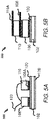
- FIG. 5A and FIG. 5B depict a reference configuration and a configuration according to the present embodiments for a device.
- a side view of wiring for a reference device 500 having a co-planar configuration of the first semiconductor die 106, in one implementation, an IGBT device, and a second semiconductor die 110, such as a diode die.
- a wire bond 122 is provided, connecting the IGBT device and diode die is series to ground.
- the first substrate 102 may be laminated with conductive layers 120, such as copper, coupled to outside voltage, on the opposite side of die from the wire bond.
- FIG. 5B depicts a side view of wiring for a device 550, according to the present embodiments.
- the diode die (second semiconductor die 110) is stacked on top of the IGBT die (first semiconductor die 106).
- the electrical connector 108 disposed between the two die, is coupled to ground, while the top surface of the diode die and the bottom surface of the IGBT die (see conductive layer 120) are coupled to external voltage.
- IGBTs may be used as high-speed switches, providing the ability to generate various type of output signals, including motor current, or sinewave type of output, at a much lower frequency than the switching speed.
- a pair of IGBT switches may operate in pulse width modulation (PWM) mode to generate an time varying output based on pulse width modulation.
- Current may be chopped between switch 1/diode 2 and switch2/diode 1, for example, generating a motor signal, such as a current signal varying as a sine wave as a function of time. As the current varies with time the degree of heating generated at the IGBT die may vary accordingly.
- PWM pulse width modulation
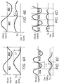
- FIG. 6A depicts a relatively lower frequency motor signal, referred to herein for convenience as "low frequency,” and resulting IGBT die temperature behavior for the reference device of FIG. 5A .
- the upper curve represents the "motor signal” or current as a function of time, while the lower signal represents the IGBT die temperature as a function of time.
- the IGBT die temperature may vary from a value T1 to a maximum temperature, represented by the dashed line.
- T1 to a maximum temperature
- FIG. 6B depicts a low frequency motor signal and resulting die assembly temperature behavior for the device of FIG. 5B .
- the motor signal may be assumed to be the same as in FIG. 6A .
- the temperature of the die assembly of FIG. 5B tends to remain higher than the device of FIG. 5A , with a minimum temperature represented by T2.
- T2 a minimum temperature represented by T2.
- the IGBT die first semiconductor die 106
- the IGBT die will tend to cool down.
- the second semiconductor die 110 that is, the diode die, is active.
- the second semiconductor die 110 is paired with another IGBT die (not shown), during the second half cycle 604, and accordingly generates additional heat, keeping the IGBT die of the device 550 warm, resulting in the second temperature peak shown in second half cycle 604.
- the overall temperature swing of the device assembly including the first semiconductor die 106 and the second semiconductor die 110, is less, shown as ⁇ T2. This lower temperature swing generates less thermal stress and may accordingly improve device reliability and longevity.
- FIG. 6C depicts a relatively higher frequency motor signal, referred to herein as "higher frequency” signal and resulting IGBT die assembly temperature behavior for the reference device of FIG. 5A .
- a first half cycle 612 and a second half cycle 614 are shown.
- the frequency of the motor signal in this example is postulated to be much higher than the frequency in the example of FIG. 6A , such as double the frequency.
- the temperature behavior of the IGBT device is qualitatively similar to the behavior of FIG. 6A , with a temperature swing of ⁇ T3 about an average temperature of T3.
- the IGBT device heats above the average temperature in the first half cycle 612 and cools below the average temperature in the second half cycle 614.
- FIG. 6D depicts a higher frequency motor signal and resulting die assembly temperature behavior for the device of FIG. 5B .
- the temperature shows a second peak in this period, and the overall temperature swing is reduced, shown as ⁇ T4.
- the PWM of the phase legs is sine-modulated to shape a sine motor current.
- the current toggles between a second transistor die in a second transistor/diode stack (T2) and a first diode die in a first transistor/diode pair (D1), whereas a second diode die in the second transistor/diode pair (D2) and a first transistor die in the first transistor/diode pair (T1) are not conducting current.
- T2 and D1 are off and D2 and T1 are conducting.
- the motor current frequency is very low (e.g., ⁇ 10Hz) the temperature of the conducting semiconductor follows the current.
- the non-current conducting semiconductors have sufficient time to cool down to the heatsink temperature.
- T2 and D1 will see a full temperature swing, while the temperature of D2 and T1 drop to the heatsink temperature.
- T1 and D2 will see a full temperature swing, while the temperature of D1 and T2 drop to the heatsink temperature.
- T2 heats up the stack during the "+wave” and, though T2 is not powered during "-wave” T2 will be heated by D2, which die is powered during "-wave".
- D2 which die is powered during "-wave”.
- the frequency of the temperature swing experienced by a transistor/diode stack doubles, and in the frequency range where the thermal capacity acts as a filter the dT will be reduced, resulting in lower stress.
- FIG. 7 depicts a process flow 700, according to embodiments of the disclosure.
- a substrate is provided.
- the main portion of the substrate may be a known material such as aluminum oxide, aluminum nitride, and so forth, according to various non-limiting embodiments, and may include conductive layers, such as known "DCB/DBC" (direct copper bond/direct bond copper substrates).
- DCB/DBC direct copper bond/direct bond copper substrates
- a first surface of an IGBT die is affixed to the substrate.
- the IGBT may be bonded to the substrate using a suitable known metallurgy according to known techniques.
- an electrical connector or lead is affixed to a second surface of the IGBT die, opposite the first surface.
- a first connector lead may be connected to an "Emitter" contact area of the IGBT die while a 2 nd connector lead is attached to a gate contact of the IGBT.
- a reverse freewheeling diode die is affixed above the electrical connector, such as the first connector lead, where the reverse freewheeling diode die is disposed directly over the IGBT die.
- the reverse freewheeling diode die has a smaller area than the area of the IGBT die and accordingly may entirely overlap with the IGBT die.
- the reverse freewheeling diode die may be centered above the IGBT die.
- the process flow may be implemented with multiple IGBT die and multiple reverse freewheeling diode die, where a given IGBT die and given reverse freewheeling diode die form a given semiconductor die assembly, such that multiple freewheeling diode die are assembled upon a given insulator substrate.
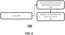
- FIG. 8 depicts another process flow, shown as process flow 750, according to additional embodiments of the disclosure.
- the process flow 750 may proceed generally as in the process flow 700, through block 702, block 704, block 706, and block 708.
- a spacer is affixed to the reverse freewheeling diode die.
- the spacer may be chosen from known spacer materials for IGBT modules.
- the thickness of the spacer may be chosen for suitable isolation.
- a second substrate is affixed to the spacer.
- the second substrate may be affixed to the spacer on a second surface of the spacer, opposite a first surface of the spacer that is used to bond to the reverse freewheeling diode die.
- the second substrate may be the same as or different from a first substrate, provided at block 702, discussed above.
- the process flow may be implemented with multiple IGBT die and multiple reverse freewheeling diode die, where a given IGBT die and given reverse freewheeling diode die form a given semiconductor die assembly, such that multiple freewheeling diode die are assembled between two insulator substrates.
Landscapes
- Inverter Devices (AREA)
- Engineering & Computer Science (AREA)
- Manufacturing & Machinery (AREA)
- Power Conversion In General (AREA)
- Cooling Or The Like Of Semiconductors Or Solid State Devices (AREA)
Abstract
Description
- Embodiments relate to the field of semiconductor devices, and in particular, packages for power semiconductor chips.
- In the present day, fast switching, power semiconductor devices normally employ fast switching diodes such as freewheeling diodes to protect the power semiconductor device from inductive loads, including motor coils or relay windings. At each instance of switching, where a switching device is turned "ON", the freewheel diode changes from a conducting state to a blocking state as it becomes reversed biased.
- However, when the device rapidly turns "OFF", the freewheeling diode becomes forward biased and the collapse of the energy stored, for example, in a coil, causes a current to flow through the freewheel diode. Without the protection of the freewheeling diode, a high di/dt current may occur, causing a high voltage spike or transient to flow, and possibly damaging the switching device.
- Accordingly, power semiconductor devices such as insulated gate bipolar transistors (IGBTs) are often arranged in power semiconductor modules, such as one or more substrates, such as 2, 4 or 6 substrates, similar to each other. Each substrate, including wires and resistors, hold pairs of IGBT die (chips) and diode chips, where one or more IGBT chips may be paired with a diode chip. This arrangement provides a modular manner to switch currents of a desirable amount by choosing the appropriate number of chips. Because the IGBT chips and diode chips are arranged in a planar configuration on a substrate, the substrates need to be sized to accommodate all of the chips, including wiring between chips. As such, power semiconductor modules may be unduly large in size to accommodate the required number of substrates and power semiconductor devices.
- In view of the above, the present embodiments are provided.
- In some embodiments, a semiconductor device module is provided. The semiconductor device module may include a first substrate; and a semiconductor die assembly, disposed on the first substrate. The semiconductor die assembly may include a first semiconductor die, bonded to the first substrate; a second semiconductor die, disposed over the first semiconductor die; and an electrical connector, disposed between the first semiconductor die and the second semiconductor die, wherein the semiconductor die assembly comprises an insulated gate bipolar transistor (IGBT) die and a freewheeling diode die.
- In another embodiment, a method of forming a semiconductor device module, may include providing a first substrate and affixing a semiconductor die assembly to the first substrate. The semiconductor die assembly may include a first semiconductor die, bonded to the first substrate; a second semiconductor die, disposed over the first semiconductor die; and an electrical connector, disposed between the first semiconductor die and the second semiconductor die, wherein the first semiconductor die assembly comprises an insulated gate bipolar transistor (IGBT) die and a freewheeling diode die.
- In an additional embodiment, a semiconductor device module may include a first substrate; and a semiconductor die assembly, disposed on the first substrate, the semiconductor die assembly comprising a stacked configuration of a first insulated gate bipolar transistor (IGBT) die and a freewheeling diode die, and an electrical connector, disposed between the IGBT die and the freewheeling diode semiconductor die. As such the IGBT die may be directly bonded to the first substrate, wherein the stacked configuration defines a first die area, equivalent to an area of the IGBT die.
-
-
FIG. 1A shows a semiconductor device module in side view, in accordance with various embodiments of the disclosure; -
FIG. 1B illustrates a top plan view of the semiconductor device module ofFIG. 1A ; -
FIG. 1C illustrates a circuit representation of a semiconductor device module according to embodiments of the disclosure; -
FIG. 2A illustrates a top plan view of another semiconductor device module according to additional embodiments of the disclosure; -
FIG. 2B illustrates a top plan view of a reference semiconductor device module; -
FIG. 3 shows another semiconductor device module in side view, in accordance with further embodiments of the disclosure; -
FIG. 4 illustrates electrical behavior during pulsing of a semiconductor device module, according to the present embodiments; -
FIG. 5A depicts a side view of wiring for a reference device having a co-planar configuration of an IGBT and diode die; -
FIG. 5B depicts a side view of wiring for a device according to the present embodiments; -
FIG. 6A depicts a relatively lower frequency motor signal and resulting IGBT die temperature behavior for the reference device ofFIG. 5A ; -
FIG. 6B depicts a relatively lower frequency motor signal and resulting die assembly temperature behavior for the device ofFIG. 6A ; -
FIG. 6C depicts a relatively higher frequency motor signal and resulting IGBT die assembly temperature behavior for the device ofFIG. 6A ; -
FIG. 6D depicts a relatively higher frequency motor signal and resulting die assembly temperature behavior for the device ofFIG. 6B ; -
FIG. 7 depicts a process flow, according to embodiments of the disclosure; and -
FIG. 8 depicts another process flow, according to additional embodiments of the disclosure. - The present embodiments will now be described more fully hereinafter with reference to the accompanying drawings, in which exemplary embodiments are shown. The embodiments are not to be construed as limited to the embodiments set forth herein. Rather, these embodiments are provided so that this disclosure will be thorough and complete, and will fully convey their scope to those skilled in the art. In the drawings, like numbers refer to like elements throughout.
- In the following description and/or claims, the terms "on," "overlying," "disposed on" and "over" may be used in the following description and claims. "On," "overlying," "disposed on" and "over" may be used to indicate that two or more elements are in direct physical contact with one another. Also, the term "on,", "overlying," "disposed on," and "over", may mean that two or more elements are not in direct contact with one another. For example, "over" may mean that one element is above another element while not contacting one another and may have another element or elements in between the two elements. Furthermore, the term "and/or" may mean "and", it may mean "or", it may mean "exclusive-or", it may mean "one", it may mean "some, but not all", it may mean "neither", and/or it may mean "both", although the scope of claimed subject matter is not limited in this respect.
- In various embodiments, a semiconductor device module and techniques for assembly are provided for power semiconductor devices.
- Turning to
FIG. 1A there is shown a side view of asemiconductor device module 100, according to various embodiments of the disclosure.FIG. 1B shows a top plan view of a variant of thesemiconductor device module 100.FIG. 1C illustrates an electrical circuit representation of thesemiconductor device module 100. Thesemiconductor device module 100 includes afirst substrate 102, asemiconductor die assembly 104, disposed on thefirst substrate 102. Thefirst substrate 102 may be a known material stack such as copper/aluminum oxide/copper also known as DCB or DBC, according to some embodiments. As such, the first substrate may include an insulator body sandwiched between metallic layers, and may be referred to as an insulator substrate. The semiconductor dieassembly 104 includes a first semiconductor die 106, attached to thefirst substrate 102, a second semiconductor die 110, disposed over the first semiconductor die 106,wire bonding 112, and anelectrical connector 108, disposed between the first semiconductor die 106 and the second semiconductor die 110. In this embodiment and other embodiments of the disclosure, thesemiconductor die assembly 104 includes an insulated gate bipolar transistor (IGBT) die and a freewheeling diode die. Generally, the IGBT die may be disposed in contact with thefirst substrate 102. As in known power device modules, an IGBT die may be coupled with a diode die, used as a freewheeling diode to protect the IGBT die. In other words, the first semiconductor die 106 may be an IGBT die, while the second semiconductor die 110 may be a freewheeling diode die. In various embodiments, the IGBT die, such as the first semiconductor die 106, is disposed over thefirst substrate 102 in a first region, and occupies a first area (in plan view, shown inFIG. 1B ), while the freewheeling diode die, such as second semiconductor die 110, occupies a second area, less than the first area. In some non-limiting embodiments, the second area may be on the order of 50% of the first area, such as 40%-60%. Notably, the second semiconductor die 110 completely overlaps the first semiconductor die 106 as shown in plan view ofFIG. 1B . As such, thesemiconductor die assembly 104 is characterized by a stacked configuration of an IGBT die and a freewheeling diode die, in contrast to known semiconductor power module configurations, where IGBT die and diode die are each arranged directly on an substrate, in a co-planar configuration. Notably, various metallic layers (not shown) may be employed to bond thesemiconductor die assembly 104 tofirst substrate 102, and to attach components within thesemiconductor die assembly 104 to one another, such as by soldering. - Notably, as shown in
FIG. 1C , the freewheeling diode die and IGBT die may be electrically coupled, wherein the freewheeling diode die is electrically coupled to the IGBT die as an inverse freewheeling diode. - In various embodiments, the stacked configuration of an IGBT die and freewheeling diode die may be provided on one or more substrates in a modular fashion. Thus, in various embodiments, the
semiconductor die assembly 104 may represent just one of multiple semiconductor die assemblies within a given semiconductor device module.FIG. 2A illustrates a top plan view of another semiconductor device module according to additional embodiments of the disclosure. Thesemiconductor device module 200 includes four separate semiconductor die assemblies, where each semiconductor die assembly may be represented bysemiconductor die assembly 104, described above. Thus, each additional semiconductor die assembly may disposed on asubstrate 202, in a manner analogous to the configuration of thesemiconductor die assembly 104, shown inFIG. 1A , where each additional semiconductor die assembly includes an insulated gate bipolar transistor (IGBT) die and a freewheeling diode die. - While a given freewheeling diode die directly lies over a given IGBT die within a
semiconductor die assembly 104, the different semiconductor die assemblies do not overlap one another, as shown inFIG. 2A . Thus, a first semiconductor die assembly, shown as semiconductor dieassembly 104A, is disposed on thesubstrate 202 in a first region, and a second semiconductor die assembly, shown as semiconductor dieassembly 104B, is disposed on thesubstrate 202 in a second region, not overlapping the first region. Said differently, the different semiconductor die assembly ofFIG. 2A are arranged in a coplanar fashion with one another. - To highlight the advantages of the
semiconductor device module 200,FIG. 2B illustrates a top plan view of a reference semiconductor device module, shown assemiconductor device module 220. This reference semiconductor device module is arranged generally according to known power semiconductor device components. In this configuration, two different semiconductor die assemblies are arranged on thesubstrate 202. The semiconductor die assemblies are represented by semiconductor die assembly 104C, where the first semiconductor die 106 and second semiconductor die 110 for a given semiconductor die assembly 104C, but are arranged in a non-stacked configuration, or co-planar configuration with one another, rather than the stacked configuration of semiconductor dieassembly 104. As shown inFIG. 2A , thesubstrate 202 is configured to accommodate thesemiconductor die assembly 104 in a stacked configuration within a first substrate area, shown as A1. As shown inFIG. 2B , the same substrate is configured to accommodate the semiconductor die assembly 104C in a second substrate area, shown as A2, where the semiconductor die assembly 104C assembly contains the same semiconductor die as in semiconductor dieassembly 104, arranged, however, in a non-stacked configuration. In accordance with various embodiments of the disclosure, the area A2 may be substantially larger than the area A1, such as at least 50% larger, and in some examples 100% larger. Said differently, the area A1, occupied by thesemiconductor die assembly 104 of the present embodiments, may be 67% of the area A2, or in some examples just 50% of the area A2. Thus, a semiconductor device module arranged with thesemiconductor die assembly 104 may be much more compact in area as compared to known semiconductor power device modules, for a given number of IGBT die. For example, as shown inFIG. 2A and FIG. 2B , the individual IGBT die, such as first semiconductor die 106, and the individual freewheeling diode die, such as second semiconductor die 110, may all be the same size, while thesubstrate 202 may be the same size inFIG. 2A and FIG. 2B . However, thesubstrate 202 ofFIG. 2A may accommodate four IGBT die in a stacked configuration, while thesubstrate 202 accommodates just two IGBT die in the non-stacked arrangement ofFIG. 2B . - While the aforementioned embodiments reflect so called single-side cooled device modules, in further embodiments, double-side cooled device modules are provided.
FIG. 3 shows another semiconductor device module in side view, in accordance with further embodiments of the disclosure. In this embodiment thesemiconductor device module 250, in addition to having the aforementioned components ofsemiconductor device module 100, includes aspacer 252, disposed over thesemiconductor die assembly 104; and asecond substrate 254, bonded to thespacer 252, where thespacer 252 is disposed between thesemiconductor die assembly 104 and thesecond substrate 254. As such, thefirst substrate 102 andsecond substrate 254 may provide double sided cooling to thesemiconductor die assembly 104. - In various additional embodiments, a plurality of semiconductor die
assemblies 104 may be arranged between afirst substrate 102 andsecond substrate 254, including thespacer 252. - Another advantage provided by the stacked configuration of a semiconductor die assembly provided by the present embodiments is the improved thermal management resulting from the stacked configuration of diode and IGBT dies.
FIG. 4 illustrates electrical behavior during pulsing of a semiconductor device module, according to the present embodiments. In the example shown, a series of regular power pulses are shown as a function of time, as well as the module temperature changes as a function of time. As illustrated, at the beginning of a pulse, a relatively rapid increase in temperature occurs, which increase may level off with time, depending upon the duration of the pulse. After the pulse terminates, a slower decrease in temperature may take place, which decrease may also level off with time, depending upon the duration of the OFF time between pulses. As such, the thermal swings may be characterized between highest and lowest temperature in one metric. According to the present embodiments, because the freewheeling diode is stacked directly over the IGBT, the overall temperature swing may be reduced for a given power switching level, in comparison to non-stacked configurations of known power modules, where the freewheeling diode is located away from the IGBT die. - To highlight the improvements in thermal swing provided by the present embodiments,
FIG. 5A and FIG. 5B depict a reference configuration and a configuration according to the present embodiments for a device. InFIG. 5A there is shown a side view of wiring for areference device 500, having a co-planar configuration of the first semiconductor die 106, in one implementation, an IGBT device, and a second semiconductor die 110, such as a diode die. Awire bond 122 is provided, connecting the IGBT device and diode die is series to ground. Thefirst substrate 102 may be laminated withconductive layers 120, such as copper, coupled to outside voltage, on the opposite side of die from the wire bond. -
FIG. 5B depicts a side view of wiring for adevice 550, according to the present embodiments. In this example, the diode die (second semiconductor die 110) is stacked on top of the IGBT die (first semiconductor die 106). Theelectrical connector 108, disposed between the two die, is coupled to ground, while the top surface of the diode die and the bottom surface of the IGBT die (see conductive layer 120) are coupled to external voltage. - As is known, in operation, IGBTs may be used as high-speed switches, providing the ability to generate various type of output signals, including motor current, or sinewave type of output, at a much lower frequency than the switching speed. A pair of IGBT switches may operate in pulse width modulation (PWM) mode to generate an time varying output based on pulse width modulation. Current may be chopped between switch 1/diode 2 and switch2/diode 1, for example, generating a motor signal, such as a current signal varying as a sine wave as a function of time. As the current varies with time the degree of heating generated at the IGBT die may vary accordingly.
FIG. 6A depicts a relatively lower frequency motor signal, referred to herein for convenience as "low frequency," and resulting IGBT die temperature behavior for the reference device ofFIG. 5A . The upper curve, represents the "motor signal" or current as a function of time, while the lower signal represents the IGBT die temperature as a function of time. In this example, the IGBT die temperature may vary from a value T1 to a maximum temperature, represented by the dashed line. In thefirst half cycle 602, the IGBT die heats up, while in thesecond half cycle 604, the IGBT die cools down. A temperature swing equal to ΔT1 occurs, as shown. -
FIG. 6B depicts a low frequency motor signal and resulting die assembly temperature behavior for the device ofFIG. 5B . In this example, the motor signal may be assumed to be the same as inFIG. 6A . Because of the stacked configuration of die, the temperature of the die assembly ofFIG. 5B tends to remain higher than the device ofFIG. 5A , with a minimum temperature represented by T2. Notably, during thefirst half cycle 602, the IGBT die (first semiconductor die 106) heats up, while in thesecond half cycle 604, the IGBT die will tend to cool down. However, during thesecond half cycle 604, the second semiconductor die 110, that is, the diode die, is active. In other words, the second semiconductor die 110 is paired with another IGBT die (not shown), during thesecond half cycle 604, and accordingly generates additional heat, keeping the IGBT die of thedevice 550 warm, resulting in the second temperature peak shown insecond half cycle 604. As a result, the overall temperature swing of the device assembly, including the first semiconductor die 106 and the second semiconductor die 110, is less, shown as ΔT2. This lower temperature swing generates less thermal stress and may accordingly improve device reliability and longevity. -
FIG. 6C depicts a relatively higher frequency motor signal, referred to herein as "higher frequency" signal and resulting IGBT die assembly temperature behavior for the reference device ofFIG. 5A . In this example, afirst half cycle 612 and asecond half cycle 614 are shown. The frequency of the motor signal in this example, is postulated to be much higher than the frequency in the example ofFIG. 6A , such as double the frequency. Notably, the temperature behavior of the IGBT device is qualitatively similar to the behavior ofFIG. 6A , with a temperature swing of ΔT3 about an average temperature of T3. Thus, the IGBT device heats above the average temperature in thefirst half cycle 612 and cools below the average temperature in thesecond half cycle 614. -
FIG. 6D depicts a higher frequency motor signal and resulting die assembly temperature behavior for the device ofFIG. 5B . Again, because the second semiconductor die 110 is active during thesecond half cycle 614, the temperature shows a second peak in this period, and the overall temperature swing is reduced, shown as ΔT4. - Notably, at ultralow frequency the number of power cycles doubles in the stacked configuration of the present embodiments. Generally, the PWM of the phase legs is sine-modulated to shape a sine motor current. Thus, in an arrangement where a first transistor/diode pair is coupled with a second transistor/diode pair, for one half period ("+ wave") the current toggles between a second transistor die in a second transistor/diode stack (T2) and a first diode die in a first transistor/diode pair (D1), whereas a second diode die in the second transistor/diode pair (D2) and a first transistor die in the first transistor/diode pair (T1) are not conducting current. In the second half period ("- wave") T2 and D1 are off and D2 and T1 are conducting. When the motor current frequency is very low (e.g., ~10Hz) the temperature of the conducting semiconductor follows the current. As frequency is very low, the non-current conducting semiconductors have sufficient time to cool down to the heatsink temperature. Thus, in the "+wave" portion T2 and D1 will see a full temperature swing, while the temperature of D2 and T1 drop to the heatsink temperature. In the "-wave" portion, T1 and D2 will see a full temperature swing, while the temperature of D1 and T2 drop to the heatsink temperature. In the present embodiments, if D2 is stacked with T2, then T2 heats up the stack during the "+wave" and, though T2 is not powered during "-wave" T2 will be heated by D2, which die is powered during "-wave". In this manner, the frequency of the temperature swing experienced by a transistor/diode stack doubles, and in the frequency range where the thermal capacity acts as a filter the dT will be reduced, resulting in lower stress.
-
FIG. 7 depicts aprocess flow 700, according to embodiments of the disclosure. At block 702 a substrate is provided. The main portion of the substrate may be a known material such as aluminum oxide, aluminum nitride, and so forth, according to various non-limiting embodiments, and may include conductive layers, such as known "DCB/DBC" (direct copper bond/direct bond copper substrates). - At
block 704, a first surface of an IGBT die is affixed to the substrate. The IGBT may be bonded to the substrate using a suitable known metallurgy according to known techniques. - At
block 706, an electrical connector or lead, is affixed to a second surface of the IGBT die, opposite the first surface. In particular, a first connector lead may be connected to an "Emitter" contact area of the IGBT die while a 2nd connector lead is attached to a gate contact of the IGBT. - At
block 708, a reverse freewheeling diode die is affixed above the electrical connector, such as the first connector lead, where the reverse freewheeling diode die is disposed directly over the IGBT die. In various embodiments, the reverse freewheeling diode die has a smaller area than the area of the IGBT die and accordingly may entirely overlap with the IGBT die. In various embodiments, the reverse freewheeling diode die may be centered above the IGBT die. - According to variants of the
process flow 700, the process flow may be implemented with multiple IGBT die and multiple reverse freewheeling diode die, where a given IGBT die and given reverse freewheeling diode die form a given semiconductor die assembly, such that multiple freewheeling diode die are assembled upon a given insulator substrate. -
FIG. 8 depicts another process flow, shown asprocess flow 750, according to additional embodiments of the disclosure. Theprocess flow 750 may proceed generally as in theprocess flow 700, throughblock 702, block 704, block 706, and block 708. Afterblock 708, atblock 760, a spacer is affixed to the reverse freewheeling diode die. The spacer may be chosen from known spacer materials for IGBT modules. The thickness of the spacer may be chosen for suitable isolation. - Subsequently to block 760, at
block 762, a second substrate is affixed to the spacer. The second substrate may be affixed to the spacer on a second surface of the spacer, opposite a first surface of the spacer that is used to bond to the reverse freewheeling diode die. Depending upon the exact design requirements the second substrate may be the same as or different from a first substrate, provided atblock 702, discussed above. - According to variants of the
process flow 750, the process flow may be implemented with multiple IGBT die and multiple reverse freewheeling diode die, where a given IGBT die and given reverse freewheeling diode die form a given semiconductor die assembly, such that multiple freewheeling diode die are assembled between two insulator substrates. - While the present embodiments have been disclosed with reference to certain embodiments, numerous modifications, alterations and changes to the described embodiments are possible while not departing from the sphere and scope of the present disclosure, as defined in the appended claims. Accordingly, the present embodiments are not to be limited to the described embodiments, and may have the full scope defined by the language of the following claims, and equivalents thereof.).
Claims (20)
- A semiconductor device module, comprising:a first substrate; anda semiconductor die assembly, disposed on the first substrate, the semiconductor die assembly comprising:a first semiconductor die, bonded to the first substrate;a second semiconductor die, disposed over the first semiconductor die; andan electrical connector, disposed between the first semiconductor die and the second semiconductor die,wherein the semiconductor die assembly comprises an insulated gate bipolar transistor (IGBT) die and a freewheeling diode die.
- The semiconductor device module of claim 1, wherein the IGBT die is directly bonded to the first substrate.
- The semiconductor device module of claim 2, wherein the IGBT die comprises a first area and is disposed over the first substrate in a first region, and the freewheeling diode die comprises a second area, less than the first area, and is disposed in the first region.
- The semiconductor device module of claim 1, wherein the freewheeling diode die is electrically coupled to the IGBT die as an inverse diode.
- The semiconductor device module of claim 1, further comprising:a spacer, disposed over the semiconductor die assembly; anda second substrate, bonded to the spacer, wherein the spacer is disposed between the semiconductor die assembly and the second substrate.
- The semiconductor device module of claim 1, wherein the semiconductor die assembly is a first semiconductor die assembly, the semiconductor device module further comprising;a second semiconductor die assembly, disposed on the first substrate, and comprising:a third semiconductor die, bonded to the first substrate;a fourth semiconductor die, disposed over the third semiconductor die; andan electrical connector, disposed between the third semiconductor die and the fourth semiconductor die,wherein the second semiconductor die assembly comprises an insulated gate bipolar transistor (IGBT) die and a freewheeling diode die.
- The semiconductor device module of claim 6, wherein the first substrate is an insulator substrate, wherein the first semiconductor die assembly is disposed on the insulator substrate in a first region, wherein the second semiconductor die assembly is disposed on the first substrate in a second region, not overlapping the first region, and wherein the first semiconductor die assembly is arranged in a coplanar fashion with the second semiconductor die assembly.
- The semiconductor device module of claim 6, the first semiconductor die assembly further comprising:a spacer, disposed over the first semiconductor die assembly and the second semiconductor die assembly; anda second substrate, bonded to the semiconductor die assembly, wherein the spacer is disposed between the semiconductor die assembly and the second substrate.
- The semiconductor device module of claim 1, further comprising at least one additional semiconductor die assembly, disposed on the substrate,wherein the semiconductor die assembly comprises a stacked configuration of the IGBT die and the freewheeling diode die,wherein each additional semiconductor die assembly of the at least one additional semiconductor die assembly comprises a stacked configuration of an additional IGBT die and an additional freewheeling diode die,wherein the first substrate is configured to accommodate the semiconductor die assembly in a stacked configuration within a first substrate area, and is configured to accommodate the at least one additional semiconductor die assembly within a second substrate area.wherein in a non-stacked configuration, a given IGBT die and given freewheeling diode die of a given semiconductor die assembly are each bonded directly to the first substrate.
- The semiconductor device module of claim 1, the semiconductor die assembly comprising a stacked semiconductor die assembly, arranged as a stacked configuration of the IGBT die and the freewheeling diode die, wherein the stacked semiconductor die assembly is configured to reduce a temperature swing during current pulsing in comparison to a non-stacked configuration of a semiconductor die assembly, wherein a given IGBT die and given freewheeling diode die are each bonded directly to the first substrate.
- A method of forming a semiconductor device module, comprising:providing a first substrate; andaffixing a semiconductor die assembly to the first substrate, the semiconductor die assembly comprising:a first semiconductor die, bonded to the first substrate;a second semiconductor die, disposed over the first semiconductor die; andan electrical connector, disposed between the first semiconductor die and the second semiconductor die,wherein the first semiconductor die assembly comprises an insulated gate bipolar transistor (IGBT) die and a freewheeling diode die.
- The method of claim 11, comprising bonding the IGBT die directly bonded to the first substrate.
- The method of claim 12, wherein the IGBT die comprises a first area and is disposed over the first substrate in a first region, and the freewheeling diode die comprises a second area, less than the first area, and is disposed in the first region.
- The method of claim 11, comprising electrically coupling the freewheeling diode die to the IGBT die as an inverse diode configuration.
- The method of claim 11, further comprising:arranging a spacer over the semiconductor die assembly; andaffixing a second substrate to the spacer, wherein the spacer is disposed between the semiconductor die assembly and the second substrate.
- The method of claim 11, wherein the semiconductor die assembly is a first semiconductor die assembly, the method further comprising;affixing a second semiconductor die assembly, over the first substrate, the second semiconductor die assembly comprising:a third semiconductor die, bonded to the first substrate;a fourth semiconductor die, disposed over the third semiconductor die; andan electrical connector, disposed between the third semiconductor die and the fourth semiconductor die,wherein the second semiconductor die assembly comprises another IGBT die and another freewheeling diode die.
- The method of claim 16, wherein the first substrate is a first insulator substrate, the method further comprising arranging the first semiconductor die assembly in a coplanar fashion with the second semiconductor die assembly, on the first insulator substrate.
- A semiconductor device module, comprising:a first substrate; anda semiconductor die assembly, disposed on the first substrate, the semiconductor die assembly comprising a stacked configuration of a first insulated gate bipolar transistor (IGBT) die and a freewheeling diode die, and an electrical connector, disposed between the IGBT die and the freewheeling diode semiconductor die,wherein the IGBT die is directly bonded to the first substrate,and wherein the stacked configuration defines a first die area, equivalent to an area of the IGBT die.
- The semiconductor device module of claim 18, further comprising:a spacer, disposed over the semiconductor die assembly; anda second substrate, bonded to the spacer, wherein the spacer is disposed between the semiconductor die assembly and the second substrate.
- The semiconductor device module of claim 18, wherein the first substrate is configured to accommodate the semiconductor die assembly in a first area A1, wherein when the IGBT die and the freewheeling diode die are arranged in a non-stacked configuration on the first substrate, the first substrate is configured to accommodate the IGBT die and the freewheeling diode die in an area A2, wherein the area A2 is at least 50% larger than A1.
Applications Claiming Priority (1)
| Application Number | Priority Date | Filing Date | Title |
|---|---|---|---|
| US16/710,630 US11037917B1 (en) | 2019-12-11 | 2019-12-11 | Semiconductor device module and method of assembly |
Publications (1)
| Publication Number | Publication Date |
|---|---|
| EP4012764A1 true EP4012764A1 (en) | 2022-06-15 |
Family
ID=73854528
Family Applications (1)
| Application Number | Title | Priority Date | Filing Date |
|---|---|---|---|
| EP20213965.5A Pending EP4012764A1 (en) | 2019-12-11 | 2020-12-14 | Semiconductor device module and method of assembly |
Country Status (4)
| Country | Link |
|---|---|
| US (2) | US11037917B1 (en) |
| EP (1) | EP4012764A1 (en) |
| JP (2) | JP2021093531A (en) |
| CN (1) | CN112951819A (en) |
Families Citing this family (2)
| Publication number | Priority date | Publication date | Assignee | Title |
|---|---|---|---|---|
| US11037917B1 (en) * | 2019-12-11 | 2021-06-15 | Littelfuse, Inc. | Semiconductor device module and method of assembly |
| KR102951806B1 (en) | 2020-10-22 | 2026-04-14 | 삼성디스플레이 주식회사 | Display device and method of fabricating the display device |
Citations (3)
| Publication number | Priority date | Publication date | Assignee | Title |
|---|---|---|---|---|
| EP1231635A1 (en) * | 2001-02-09 | 2002-08-14 | STMicroelectronics S.r.l. | Method for manufacturing an electronic power device and a diode in a same package |
| US20070200219A1 (en) * | 2006-02-21 | 2007-08-30 | Ralf Otremba | Power Semiconductor Device And Method For Producing It |
| EP2899756A1 (en) * | 2012-09-19 | 2015-07-29 | Micro Module Technology Co., Ltd. | Semiconductor device |
Family Cites Families (28)
| Publication number | Priority date | Publication date | Assignee | Title |
|---|---|---|---|---|
| JP4140238B2 (en) * | 2001-12-26 | 2008-08-27 | トヨタ自動車株式会社 | Semiconductor module bonding structure |
| JP3850739B2 (en) * | 2002-02-21 | 2006-11-29 | 三菱電機株式会社 | Semiconductor device |
| DE10317580B4 (en) * | 2002-04-18 | 2010-09-16 | Hitachi, Ltd. | Electric inverter device with a liquid channel and electric vehicle with such an inverter device |
| JP4164409B2 (en) * | 2003-06-13 | 2008-10-15 | 三菱電機株式会社 | Semiconductor power module |
| US7757392B2 (en) * | 2006-05-17 | 2010-07-20 | Infineon Technologies Ag | Method of producing an electronic component |
| JP4973059B2 (en) * | 2006-08-09 | 2012-07-11 | 日産自動車株式会社 | Semiconductor device and power conversion device |
| JP5028907B2 (en) * | 2006-08-11 | 2012-09-19 | 日産自動車株式会社 | Semiconductor device and power conversion device |
| US9147644B2 (en) * | 2008-02-26 | 2015-09-29 | International Rectifier Corporation | Semiconductor device and passive component integration in a semiconductor package |
| JP2011036017A (en) * | 2009-07-31 | 2011-02-17 | Daikin Industries Ltd | Power conversion apparatus |
| US8637981B2 (en) * | 2011-03-30 | 2014-01-28 | International Rectifier Corporation | Dual compartment semiconductor package with temperature sensor |
| US8987777B2 (en) * | 2011-07-11 | 2015-03-24 | International Rectifier Corporation | Stacked half-bridge power module |
| US20190097524A1 (en) * | 2011-09-13 | 2019-03-28 | Fsp Technology Inc. | Circuit having snubber circuit in power supply device |
| KR101289196B1 (en) * | 2011-09-14 | 2013-07-26 | 삼성전기주식회사 | Power Module Package and Method for Manufacturing the same |
| US10290566B2 (en) * | 2014-09-23 | 2019-05-14 | Infineon Technologies Austria Ag | Electronic component |
| US9666677B1 (en) * | 2014-12-23 | 2017-05-30 | Soraa Laser Diode, Inc. | Manufacturable thin film gallium and nitrogen containing devices |
| ITUB20153344A1 (en) * | 2015-09-02 | 2017-03-02 | St Microelectronics Srl | ELECTRONIC POWER MODULE WITH IMPROVED THERMAL DISSIPATION AND ITS MANUFACTURING METHOD |
| DE102015012915B4 (en) * | 2015-10-06 | 2020-10-15 | Audi Ag | Arrangement of semiconductor elements on a semiconductor module for a power module or a corresponding method |
| KR101956983B1 (en) * | 2016-09-20 | 2019-03-11 | 현대자동차일본기술연구소 | Power module and manufacturing method therefor |
| JP2018064362A (en) * | 2016-10-12 | 2018-04-19 | 学校法人早稲田大学 | Semiconductor device |
| EP3376539A1 (en) * | 2017-03-14 | 2018-09-19 | HS Elektronik Systeme GmbH | Stackable power module |
| JP6845818B2 (en) * | 2018-02-09 | 2021-03-24 | 株式会社Soken | Drive device for rotary electric machine |
| US20190371891A1 (en) * | 2018-06-01 | 2019-12-05 | Qualcomm Incorporated | Bulk layer transfer based switch with backside silicidation |
| US10727268B1 (en) * | 2019-01-25 | 2020-07-28 | Smartsens Technology (Cayman) Co., Ltd | CMOS image sensor with compact pixel layout |
| US20210013176A1 (en) * | 2019-07-09 | 2021-01-14 | Semiconductor Components Industries, Llc | Pre-stacking mechanical strength enhancement of power device structures |
| US11037917B1 (en) * | 2019-12-11 | 2021-06-15 | Littelfuse, Inc. | Semiconductor device module and method of assembly |
| US11282764B2 (en) * | 2020-02-07 | 2022-03-22 | Semiconductor Components Industries, Llc | Structure and method related to a power module using a hybrid spacer |
| US10897251B1 (en) * | 2020-04-20 | 2021-01-19 | Infineon Technologies Austria Ag | Isolation barrier communication system in a package for isolated gate driver communication |
| US11521907B2 (en) * | 2020-10-14 | 2022-12-06 | Infineon Technologies Ag | Hybrid embedded package |
-
2019
- 2019-12-11 US US16/710,630 patent/US11037917B1/en active Active
-
2020
- 2020-12-08 JP JP2020203770A patent/JP2021093531A/en active Pending
- 2020-12-11 CN CN202011458721.9A patent/CN112951819A/en active Pending
- 2020-12-14 EP EP20213965.5A patent/EP4012764A1/en active Pending
-
2021
- 2021-05-10 US US17/315,714 patent/US11545479B2/en active Active
-
2025
- 2025-10-30 JP JP2025183599A patent/JP2026012912A/en active Pending
Patent Citations (3)
| Publication number | Priority date | Publication date | Assignee | Title |
|---|---|---|---|---|
| EP1231635A1 (en) * | 2001-02-09 | 2002-08-14 | STMicroelectronics S.r.l. | Method for manufacturing an electronic power device and a diode in a same package |
| US20070200219A1 (en) * | 2006-02-21 | 2007-08-30 | Ralf Otremba | Power Semiconductor Device And Method For Producing It |
| EP2899756A1 (en) * | 2012-09-19 | 2015-07-29 | Micro Module Technology Co., Ltd. | Semiconductor device |
Also Published As
| Publication number | Publication date |
|---|---|
| JP2021093531A (en) | 2021-06-17 |
| US11037917B1 (en) | 2021-06-15 |
| US11545479B2 (en) | 2023-01-03 |
| CN112951819A (en) | 2021-06-11 |
| JP2026012912A (en) | 2026-01-27 |
| US20210265332A1 (en) | 2021-08-26 |
| US20210183841A1 (en) | 2021-06-17 |
Similar Documents
| Publication | Publication Date | Title |
|---|---|---|
| Robles et al. | The role of power device technology in the electric vehicle powertrain | |
| US10522517B2 (en) | Half-bridge power semiconductor module and manufacturing method therefor | |
| US10784213B2 (en) | Power device package | |
| US5574312A (en) | Low-inductance power semiconductor module | |
| CN205789962U (en) | Circuit and packaged type electronic equipment | |
| JP7642714B2 (en) | Semiconductor Device | |
| US7291869B2 (en) | Electronic module with stacked semiconductors | |
| US7633141B2 (en) | Semiconductor device having through contact blocks with external contact areas | |
| US20130015495A1 (en) | Stacked Half-Bridge Power Module | |
| WO2015176985A1 (en) | Semiconductor power module with low stray inductance | |
| JP2026012912A (en) | Semiconductor device module and assembly method | |
| CN105720046A (en) | Semiconductor module and semiconductor device | |
| JP2012175070A (en) | Semiconductor package | |
| JPWO2016129097A1 (en) | Half-bridge power semiconductor module and manufacturing method thereof | |
| WO2022017789A1 (en) | Switching components | |
| Chen et al. | 3.3 kV low-inductance full SiC power module | |
| JP7118204B1 (en) | semiconductor equipment | |
| JP6331543B2 (en) | Half-bridge power semiconductor module and manufacturing method thereof | |
| JP4096741B2 (en) | Semiconductor device | |
| US20230253391A1 (en) | Half-bridge module with reversed diodes | |
| CN108323211A (en) | Power device package | |
| JP4706551B2 (en) | Power semiconductor element and power module | |
| KR101754923B1 (en) | Power module based on high electron mobility transistors | |
| JP3525823B2 (en) | Mounting structure of complementary IGBT | |
| KR20230095546A (en) | Power semiconductor module and its manufacturing method |
Legal Events
| Date | Code | Title | Description |
|---|---|---|---|
| PUAI | Public reference made under article 153(3) epc to a published international application that has entered the european phase |
Free format text: ORIGINAL CODE: 0009012 |
|
| STAA | Information on the status of an ep patent application or granted ep patent |
Free format text: STATUS: THE APPLICATION HAS BEEN PUBLISHED |
|
| AK | Designated contracting states |
Kind code of ref document: A1 Designated state(s): AL AT BE BG CH CY CZ DE DK EE ES FI FR GB GR HR HU IE IS IT LI LT LU LV MC MK MT NL NO PL PT RO RS SE SI SK SM TR |
|
| STAA | Information on the status of an ep patent application or granted ep patent |
Free format text: STATUS: REQUEST FOR EXAMINATION WAS MADE |
|
| 17P | Request for examination filed |
Effective date: 20221201 |
|
| RBV | Designated contracting states (corrected) |
Designated state(s): AL AT BE BG CH CY CZ DE DK EE ES FI FR GB GR HR HU IE IS IT LI LT LU LV MC MK MT NL NO PL PT RO RS SE SI SK SM TR |