EP4012752A1 - Stage and method for controlling temperature of substrate - Google Patents
Stage and method for controlling temperature of substrate Download PDFInfo
- Publication number
- EP4012752A1 EP4012752A1 EP20850947.1A EP20850947A EP4012752A1 EP 4012752 A1 EP4012752 A1 EP 4012752A1 EP 20850947 A EP20850947 A EP 20850947A EP 4012752 A1 EP4012752 A1 EP 4012752A1
- Authority
- EP
- European Patent Office
- Prior art keywords
- supporting plate
- gas
- stage
- substrate
- chamber
- Prior art date
- Legal status (The legal status is an assumption and is not a legal conclusion. Google has not performed a legal analysis and makes no representation as to the accuracy of the status listed.)
- Pending
Links
Images



Classifications
-
- H—ELECTRICITY
- H10—SEMICONDUCTOR DEVICES; ELECTRIC SOLID-STATE DEVICES NOT OTHERWISE PROVIDED FOR
- H10P—GENERIC PROCESSES OR APPARATUS FOR THE MANUFACTURE OR TREATMENT OF DEVICES COVERED BY CLASS H10
- H10P72/00—Handling or holding of wafers, substrates or devices during manufacture or treatment thereof
- H10P72/04—Apparatus for manufacture or treatment
- H10P72/0431—Apparatus for thermal treatment
- H10P72/0432—Apparatus for thermal treatment mainly by conduction
-
- C—CHEMISTRY; METALLURGY
- C23—COATING METALLIC MATERIAL; COATING MATERIAL WITH METALLIC MATERIAL; CHEMICAL SURFACE TREATMENT; DIFFUSION TREATMENT OF METALLIC MATERIAL; COATING BY VACUUM EVAPORATION, BY SPUTTERING, BY ION IMPLANTATION OR BY CHEMICAL VAPOUR DEPOSITION, IN GENERAL; INHIBITING CORROSION OF METALLIC MATERIAL OR INCRUSTATION IN GENERAL
- C23C—COATING METALLIC MATERIAL; COATING MATERIAL WITH METALLIC MATERIAL; SURFACE TREATMENT OF METALLIC MATERIAL BY DIFFUSION INTO THE SURFACE, BY CHEMICAL CONVERSION OR SUBSTITUTION; COATING BY VACUUM EVAPORATION, BY SPUTTERING, BY ION IMPLANTATION OR BY CHEMICAL VAPOUR DEPOSITION, IN GENERAL
- C23C14/00—Coating by vacuum evaporation, by sputtering or by ion implantation of the coating forming material
- C23C14/04—Coating on selected surface areas, e.g. using masks
- C23C14/042—Coating on selected surface areas, e.g. using masks using masks
-
- C—CHEMISTRY; METALLURGY
- C23—COATING METALLIC MATERIAL; COATING MATERIAL WITH METALLIC MATERIAL; CHEMICAL SURFACE TREATMENT; DIFFUSION TREATMENT OF METALLIC MATERIAL; COATING BY VACUUM EVAPORATION, BY SPUTTERING, BY ION IMPLANTATION OR BY CHEMICAL VAPOUR DEPOSITION, IN GENERAL; INHIBITING CORROSION OF METALLIC MATERIAL OR INCRUSTATION IN GENERAL
- C23C—COATING METALLIC MATERIAL; COATING MATERIAL WITH METALLIC MATERIAL; SURFACE TREATMENT OF METALLIC MATERIAL BY DIFFUSION INTO THE SURFACE, BY CHEMICAL CONVERSION OR SUBSTITUTION; COATING BY VACUUM EVAPORATION, BY SPUTTERING, BY ION IMPLANTATION OR BY CHEMICAL VAPOUR DEPOSITION, IN GENERAL
- C23C14/00—Coating by vacuum evaporation, by sputtering or by ion implantation of the coating forming material
- C23C14/22—Coating by vacuum evaporation, by sputtering or by ion implantation of the coating forming material characterised by the process of coating
- C23C14/24—Vacuum evaporation
-
- C—CHEMISTRY; METALLURGY
- C23—COATING METALLIC MATERIAL; COATING MATERIAL WITH METALLIC MATERIAL; CHEMICAL SURFACE TREATMENT; DIFFUSION TREATMENT OF METALLIC MATERIAL; COATING BY VACUUM EVAPORATION, BY SPUTTERING, BY ION IMPLANTATION OR BY CHEMICAL VAPOUR DEPOSITION, IN GENERAL; INHIBITING CORROSION OF METALLIC MATERIAL OR INCRUSTATION IN GENERAL
- C23C—COATING METALLIC MATERIAL; COATING MATERIAL WITH METALLIC MATERIAL; SURFACE TREATMENT OF METALLIC MATERIAL BY DIFFUSION INTO THE SURFACE, BY CHEMICAL CONVERSION OR SUBSTITUTION; COATING BY VACUUM EVAPORATION, BY SPUTTERING, BY ION IMPLANTATION OR BY CHEMICAL VAPOUR DEPOSITION, IN GENERAL
- C23C14/00—Coating by vacuum evaporation, by sputtering or by ion implantation of the coating forming material
- C23C14/22—Coating by vacuum evaporation, by sputtering or by ion implantation of the coating forming material characterised by the process of coating
- C23C14/34—Sputtering
-
- C—CHEMISTRY; METALLURGY
- C23—COATING METALLIC MATERIAL; COATING MATERIAL WITH METALLIC MATERIAL; CHEMICAL SURFACE TREATMENT; DIFFUSION TREATMENT OF METALLIC MATERIAL; COATING BY VACUUM EVAPORATION, BY SPUTTERING, BY ION IMPLANTATION OR BY CHEMICAL VAPOUR DEPOSITION, IN GENERAL; INHIBITING CORROSION OF METALLIC MATERIAL OR INCRUSTATION IN GENERAL
- C23C—COATING METALLIC MATERIAL; COATING MATERIAL WITH METALLIC MATERIAL; SURFACE TREATMENT OF METALLIC MATERIAL BY DIFFUSION INTO THE SURFACE, BY CHEMICAL CONVERSION OR SUBSTITUTION; COATING BY VACUUM EVAPORATION, BY SPUTTERING, BY ION IMPLANTATION OR BY CHEMICAL VAPOUR DEPOSITION, IN GENERAL
- C23C14/00—Coating by vacuum evaporation, by sputtering or by ion implantation of the coating forming material
- C23C14/22—Coating by vacuum evaporation, by sputtering or by ion implantation of the coating forming material characterised by the process of coating
- C23C14/50—Substrate holders
-
- C—CHEMISTRY; METALLURGY
- C23—COATING METALLIC MATERIAL; COATING MATERIAL WITH METALLIC MATERIAL; CHEMICAL SURFACE TREATMENT; DIFFUSION TREATMENT OF METALLIC MATERIAL; COATING BY VACUUM EVAPORATION, BY SPUTTERING, BY ION IMPLANTATION OR BY CHEMICAL VAPOUR DEPOSITION, IN GENERAL; INHIBITING CORROSION OF METALLIC MATERIAL OR INCRUSTATION IN GENERAL
- C23C—COATING METALLIC MATERIAL; COATING MATERIAL WITH METALLIC MATERIAL; SURFACE TREATMENT OF METALLIC MATERIAL BY DIFFUSION INTO THE SURFACE, BY CHEMICAL CONVERSION OR SUBSTITUTION; COATING BY VACUUM EVAPORATION, BY SPUTTERING, BY ION IMPLANTATION OR BY CHEMICAL VAPOUR DEPOSITION, IN GENERAL
- C23C14/00—Coating by vacuum evaporation, by sputtering or by ion implantation of the coating forming material
- C23C14/22—Coating by vacuum evaporation, by sputtering or by ion implantation of the coating forming material characterised by the process of coating
- C23C14/50—Substrate holders
- C23C14/505—Substrate holders for rotation of the substrates
-
- C—CHEMISTRY; METALLURGY
- C23—COATING METALLIC MATERIAL; COATING MATERIAL WITH METALLIC MATERIAL; CHEMICAL SURFACE TREATMENT; DIFFUSION TREATMENT OF METALLIC MATERIAL; COATING BY VACUUM EVAPORATION, BY SPUTTERING, BY ION IMPLANTATION OR BY CHEMICAL VAPOUR DEPOSITION, IN GENERAL; INHIBITING CORROSION OF METALLIC MATERIAL OR INCRUSTATION IN GENERAL
- C23C—COATING METALLIC MATERIAL; COATING MATERIAL WITH METALLIC MATERIAL; SURFACE TREATMENT OF METALLIC MATERIAL BY DIFFUSION INTO THE SURFACE, BY CHEMICAL CONVERSION OR SUBSTITUTION; COATING BY VACUUM EVAPORATION, BY SPUTTERING, BY ION IMPLANTATION OR BY CHEMICAL VAPOUR DEPOSITION, IN GENERAL
- C23C14/00—Coating by vacuum evaporation, by sputtering or by ion implantation of the coating forming material
- C23C14/22—Coating by vacuum evaporation, by sputtering or by ion implantation of the coating forming material characterised by the process of coating
- C23C14/54—Controlling or regulating the coating process
- C23C14/541—Heating or cooling of the substrates
-
- C—CHEMISTRY; METALLURGY
- C23—COATING METALLIC MATERIAL; COATING MATERIAL WITH METALLIC MATERIAL; CHEMICAL SURFACE TREATMENT; DIFFUSION TREATMENT OF METALLIC MATERIAL; COATING BY VACUUM EVAPORATION, BY SPUTTERING, BY ION IMPLANTATION OR BY CHEMICAL VAPOUR DEPOSITION, IN GENERAL; INHIBITING CORROSION OF METALLIC MATERIAL OR INCRUSTATION IN GENERAL
- C23C—COATING METALLIC MATERIAL; COATING MATERIAL WITH METALLIC MATERIAL; SURFACE TREATMENT OF METALLIC MATERIAL BY DIFFUSION INTO THE SURFACE, BY CHEMICAL CONVERSION OR SUBSTITUTION; COATING BY VACUUM EVAPORATION, BY SPUTTERING, BY ION IMPLANTATION OR BY CHEMICAL VAPOUR DEPOSITION, IN GENERAL
- C23C16/00—Chemical coating by decomposition of gaseous compounds, without leaving reaction products of surface material in the coating, i.e. chemical vapour deposition [CVD] processes
- C23C16/06—Chemical coating by decomposition of gaseous compounds, without leaving reaction products of surface material in the coating, i.e. chemical vapour deposition [CVD] processes characterised by the deposition of metallic material
- C23C16/18—Chemical coating by decomposition of gaseous compounds, without leaving reaction products of surface material in the coating, i.e. chemical vapour deposition [CVD] processes characterised by the deposition of metallic material from metallo-organic compounds
-
- C—CHEMISTRY; METALLURGY
- C23—COATING METALLIC MATERIAL; COATING MATERIAL WITH METALLIC MATERIAL; CHEMICAL SURFACE TREATMENT; DIFFUSION TREATMENT OF METALLIC MATERIAL; COATING BY VACUUM EVAPORATION, BY SPUTTERING, BY ION IMPLANTATION OR BY CHEMICAL VAPOUR DEPOSITION, IN GENERAL; INHIBITING CORROSION OF METALLIC MATERIAL OR INCRUSTATION IN GENERAL
- C23C—COATING METALLIC MATERIAL; COATING MATERIAL WITH METALLIC MATERIAL; SURFACE TREATMENT OF METALLIC MATERIAL BY DIFFUSION INTO THE SURFACE, BY CHEMICAL CONVERSION OR SUBSTITUTION; COATING BY VACUUM EVAPORATION, BY SPUTTERING, BY ION IMPLANTATION OR BY CHEMICAL VAPOUR DEPOSITION, IN GENERAL
- C23C16/00—Chemical coating by decomposition of gaseous compounds, without leaving reaction products of surface material in the coating, i.e. chemical vapour deposition [CVD] processes
- C23C16/06—Chemical coating by decomposition of gaseous compounds, without leaving reaction products of surface material in the coating, i.e. chemical vapour deposition [CVD] processes characterised by the deposition of metallic material
- C23C16/18—Chemical coating by decomposition of gaseous compounds, without leaving reaction products of surface material in the coating, i.e. chemical vapour deposition [CVD] processes characterised by the deposition of metallic material from metallo-organic compounds
- C23C16/20—Deposition of aluminium only
-
- C—CHEMISTRY; METALLURGY
- C23—COATING METALLIC MATERIAL; COATING MATERIAL WITH METALLIC MATERIAL; CHEMICAL SURFACE TREATMENT; DIFFUSION TREATMENT OF METALLIC MATERIAL; COATING BY VACUUM EVAPORATION, BY SPUTTERING, BY ION IMPLANTATION OR BY CHEMICAL VAPOUR DEPOSITION, IN GENERAL; INHIBITING CORROSION OF METALLIC MATERIAL OR INCRUSTATION IN GENERAL
- C23C—COATING METALLIC MATERIAL; COATING MATERIAL WITH METALLIC MATERIAL; SURFACE TREATMENT OF METALLIC MATERIAL BY DIFFUSION INTO THE SURFACE, BY CHEMICAL CONVERSION OR SUBSTITUTION; COATING BY VACUUM EVAPORATION, BY SPUTTERING, BY ION IMPLANTATION OR BY CHEMICAL VAPOUR DEPOSITION, IN GENERAL
- C23C16/00—Chemical coating by decomposition of gaseous compounds, without leaving reaction products of surface material in the coating, i.e. chemical vapour deposition [CVD] processes
- C23C16/44—Chemical coating by decomposition of gaseous compounds, without leaving reaction products of surface material in the coating, i.e. chemical vapour deposition [CVD] processes characterised by the method of coating
- C23C16/4412—Details relating to the exhausts, e.g. pumps, filters, scrubbers, particle traps
-
- C—CHEMISTRY; METALLURGY
- C23—COATING METALLIC MATERIAL; COATING MATERIAL WITH METALLIC MATERIAL; CHEMICAL SURFACE TREATMENT; DIFFUSION TREATMENT OF METALLIC MATERIAL; COATING BY VACUUM EVAPORATION, BY SPUTTERING, BY ION IMPLANTATION OR BY CHEMICAL VAPOUR DEPOSITION, IN GENERAL; INHIBITING CORROSION OF METALLIC MATERIAL OR INCRUSTATION IN GENERAL
- C23C—COATING METALLIC MATERIAL; COATING MATERIAL WITH METALLIC MATERIAL; SURFACE TREATMENT OF METALLIC MATERIAL BY DIFFUSION INTO THE SURFACE, BY CHEMICAL CONVERSION OR SUBSTITUTION; COATING BY VACUUM EVAPORATION, BY SPUTTERING, BY ION IMPLANTATION OR BY CHEMICAL VAPOUR DEPOSITION, IN GENERAL
- C23C16/00—Chemical coating by decomposition of gaseous compounds, without leaving reaction products of surface material in the coating, i.e. chemical vapour deposition [CVD] processes
- C23C16/44—Chemical coating by decomposition of gaseous compounds, without leaving reaction products of surface material in the coating, i.e. chemical vapour deposition [CVD] processes characterised by the method of coating
- C23C16/455—Chemical coating by decomposition of gaseous compounds, without leaving reaction products of surface material in the coating, i.e. chemical vapour deposition [CVD] processes characterised by the method of coating characterised by the method used for introducing gases into reaction chamber or for modifying gas flows in reaction chamber
-
- C—CHEMISTRY; METALLURGY
- C23—COATING METALLIC MATERIAL; COATING MATERIAL WITH METALLIC MATERIAL; CHEMICAL SURFACE TREATMENT; DIFFUSION TREATMENT OF METALLIC MATERIAL; COATING BY VACUUM EVAPORATION, BY SPUTTERING, BY ION IMPLANTATION OR BY CHEMICAL VAPOUR DEPOSITION, IN GENERAL; INHIBITING CORROSION OF METALLIC MATERIAL OR INCRUSTATION IN GENERAL
- C23C—COATING METALLIC MATERIAL; COATING MATERIAL WITH METALLIC MATERIAL; SURFACE TREATMENT OF METALLIC MATERIAL BY DIFFUSION INTO THE SURFACE, BY CHEMICAL CONVERSION OR SUBSTITUTION; COATING BY VACUUM EVAPORATION, BY SPUTTERING, BY ION IMPLANTATION OR BY CHEMICAL VAPOUR DEPOSITION, IN GENERAL
- C23C16/00—Chemical coating by decomposition of gaseous compounds, without leaving reaction products of surface material in the coating, i.e. chemical vapour deposition [CVD] processes
- C23C16/44—Chemical coating by decomposition of gaseous compounds, without leaving reaction products of surface material in the coating, i.e. chemical vapour deposition [CVD] processes characterised by the method of coating
- C23C16/458—Chemical coating by decomposition of gaseous compounds, without leaving reaction products of surface material in the coating, i.e. chemical vapour deposition [CVD] processes characterised by the method of coating characterised by the method used for supporting substrates in the reaction chamber
- C23C16/4581—Chemical coating by decomposition of gaseous compounds, without leaving reaction products of surface material in the coating, i.e. chemical vapour deposition [CVD] processes characterised by the method of coating characterised by the method used for supporting substrates in the reaction chamber characterised by material of construction or surface finish of the means for supporting the substrate
-
- C—CHEMISTRY; METALLURGY
- C23—COATING METALLIC MATERIAL; COATING MATERIAL WITH METALLIC MATERIAL; CHEMICAL SURFACE TREATMENT; DIFFUSION TREATMENT OF METALLIC MATERIAL; COATING BY VACUUM EVAPORATION, BY SPUTTERING, BY ION IMPLANTATION OR BY CHEMICAL VAPOUR DEPOSITION, IN GENERAL; INHIBITING CORROSION OF METALLIC MATERIAL OR INCRUSTATION IN GENERAL
- C23C—COATING METALLIC MATERIAL; COATING MATERIAL WITH METALLIC MATERIAL; SURFACE TREATMENT OF METALLIC MATERIAL BY DIFFUSION INTO THE SURFACE, BY CHEMICAL CONVERSION OR SUBSTITUTION; COATING BY VACUUM EVAPORATION, BY SPUTTERING, BY ION IMPLANTATION OR BY CHEMICAL VAPOUR DEPOSITION, IN GENERAL
- C23C16/00—Chemical coating by decomposition of gaseous compounds, without leaving reaction products of surface material in the coating, i.e. chemical vapour deposition [CVD] processes
- C23C16/44—Chemical coating by decomposition of gaseous compounds, without leaving reaction products of surface material in the coating, i.e. chemical vapour deposition [CVD] processes characterised by the method of coating
- C23C16/458—Chemical coating by decomposition of gaseous compounds, without leaving reaction products of surface material in the coating, i.e. chemical vapour deposition [CVD] processes characterised by the method of coating characterised by the method used for supporting substrates in the reaction chamber
- C23C16/4582—Rigid and flat substrates, e.g. plates or discs
- C23C16/4583—Rigid and flat substrates, e.g. plates or discs the substrate being supported substantially horizontally
- C23C16/4586—Elements in the interior of the support, e.g. electrodes, heating or cooling devices
-
- C—CHEMISTRY; METALLURGY
- C23—COATING METALLIC MATERIAL; COATING MATERIAL WITH METALLIC MATERIAL; CHEMICAL SURFACE TREATMENT; DIFFUSION TREATMENT OF METALLIC MATERIAL; COATING BY VACUUM EVAPORATION, BY SPUTTERING, BY ION IMPLANTATION OR BY CHEMICAL VAPOUR DEPOSITION, IN GENERAL; INHIBITING CORROSION OF METALLIC MATERIAL OR INCRUSTATION IN GENERAL
- C23C—COATING METALLIC MATERIAL; COATING MATERIAL WITH METALLIC MATERIAL; SURFACE TREATMENT OF METALLIC MATERIAL BY DIFFUSION INTO THE SURFACE, BY CHEMICAL CONVERSION OR SUBSTITUTION; COATING BY VACUUM EVAPORATION, BY SPUTTERING, BY ION IMPLANTATION OR BY CHEMICAL VAPOUR DEPOSITION, IN GENERAL
- C23C16/00—Chemical coating by decomposition of gaseous compounds, without leaving reaction products of surface material in the coating, i.e. chemical vapour deposition [CVD] processes
- C23C16/44—Chemical coating by decomposition of gaseous compounds, without leaving reaction products of surface material in the coating, i.e. chemical vapour deposition [CVD] processes characterised by the method of coating
- C23C16/46—Chemical coating by decomposition of gaseous compounds, without leaving reaction products of surface material in the coating, i.e. chemical vapour deposition [CVD] processes characterised by the method of coating characterised by the method used for heating the substrate
-
- C—CHEMISTRY; METALLURGY
- C23—COATING METALLIC MATERIAL; COATING MATERIAL WITH METALLIC MATERIAL; CHEMICAL SURFACE TREATMENT; DIFFUSION TREATMENT OF METALLIC MATERIAL; COATING BY VACUUM EVAPORATION, BY SPUTTERING, BY ION IMPLANTATION OR BY CHEMICAL VAPOUR DEPOSITION, IN GENERAL; INHIBITING CORROSION OF METALLIC MATERIAL OR INCRUSTATION IN GENERAL
- C23C—COATING METALLIC MATERIAL; COATING MATERIAL WITH METALLIC MATERIAL; SURFACE TREATMENT OF METALLIC MATERIAL BY DIFFUSION INTO THE SURFACE, BY CHEMICAL CONVERSION OR SUBSTITUTION; COATING BY VACUUM EVAPORATION, BY SPUTTERING, BY ION IMPLANTATION OR BY CHEMICAL VAPOUR DEPOSITION, IN GENERAL
- C23C16/00—Chemical coating by decomposition of gaseous compounds, without leaving reaction products of surface material in the coating, i.e. chemical vapour deposition [CVD] processes
- C23C16/44—Chemical coating by decomposition of gaseous compounds, without leaving reaction products of surface material in the coating, i.e. chemical vapour deposition [CVD] processes characterised by the method of coating
- C23C16/46—Chemical coating by decomposition of gaseous compounds, without leaving reaction products of surface material in the coating, i.e. chemical vapour deposition [CVD] processes characterised by the method of coating characterised by the method used for heating the substrate
- C23C16/463—Cooling of the substrate
-
- C—CHEMISTRY; METALLURGY
- C23—COATING METALLIC MATERIAL; COATING MATERIAL WITH METALLIC MATERIAL; CHEMICAL SURFACE TREATMENT; DIFFUSION TREATMENT OF METALLIC MATERIAL; COATING BY VACUUM EVAPORATION, BY SPUTTERING, BY ION IMPLANTATION OR BY CHEMICAL VAPOUR DEPOSITION, IN GENERAL; INHIBITING CORROSION OF METALLIC MATERIAL OR INCRUSTATION IN GENERAL
- C23C—COATING METALLIC MATERIAL; COATING MATERIAL WITH METALLIC MATERIAL; SURFACE TREATMENT OF METALLIC MATERIAL BY DIFFUSION INTO THE SURFACE, BY CHEMICAL CONVERSION OR SUBSTITUTION; COATING BY VACUUM EVAPORATION, BY SPUTTERING, BY ION IMPLANTATION OR BY CHEMICAL VAPOUR DEPOSITION, IN GENERAL
- C23C16/00—Chemical coating by decomposition of gaseous compounds, without leaving reaction products of surface material in the coating, i.e. chemical vapour deposition [CVD] processes
- C23C16/44—Chemical coating by decomposition of gaseous compounds, without leaving reaction products of surface material in the coating, i.e. chemical vapour deposition [CVD] processes characterised by the method of coating
- C23C16/50—Chemical coating by decomposition of gaseous compounds, without leaving reaction products of surface material in the coating, i.e. chemical vapour deposition [CVD] processes characterised by the method of coating using electric discharges
- C23C16/511—Chemical coating by decomposition of gaseous compounds, without leaving reaction products of surface material in the coating, i.e. chemical vapour deposition [CVD] processes characterised by the method of coating using electric discharges using microwave discharges
-
- C—CHEMISTRY; METALLURGY
- C23—COATING METALLIC MATERIAL; COATING MATERIAL WITH METALLIC MATERIAL; CHEMICAL SURFACE TREATMENT; DIFFUSION TREATMENT OF METALLIC MATERIAL; COATING BY VACUUM EVAPORATION, BY SPUTTERING, BY ION IMPLANTATION OR BY CHEMICAL VAPOUR DEPOSITION, IN GENERAL; INHIBITING CORROSION OF METALLIC MATERIAL OR INCRUSTATION IN GENERAL
- C23C—COATING METALLIC MATERIAL; COATING MATERIAL WITH METALLIC MATERIAL; SURFACE TREATMENT OF METALLIC MATERIAL BY DIFFUSION INTO THE SURFACE, BY CHEMICAL CONVERSION OR SUBSTITUTION; COATING BY VACUUM EVAPORATION, BY SPUTTERING, BY ION IMPLANTATION OR BY CHEMICAL VAPOUR DEPOSITION, IN GENERAL
- C23C16/00—Chemical coating by decomposition of gaseous compounds, without leaving reaction products of surface material in the coating, i.e. chemical vapour deposition [CVD] processes
- C23C16/44—Chemical coating by decomposition of gaseous compounds, without leaving reaction products of surface material in the coating, i.e. chemical vapour deposition [CVD] processes characterised by the method of coating
- C23C16/52—Controlling or regulating the coating process
-
- H—ELECTRICITY
- H01—ELECTRIC ELEMENTS
- H01J—ELECTRIC DISCHARGE TUBES OR DISCHARGE LAMPS
- H01J37/00—Discharge tubes with provision for introducing objects or material to be exposed to the discharge, e.g. for the purpose of examination or processing thereof
- H01J37/32—Gas-filled discharge tubes
- H01J37/32431—Constructional details of the reactor
- H01J37/3244—Gas supply means
- H01J37/32449—Gas control, e.g. control of the gas flow
-
- H—ELECTRICITY
- H01—ELECTRIC ELEMENTS
- H01J—ELECTRIC DISCHARGE TUBES OR DISCHARGE LAMPS
- H01J37/00—Discharge tubes with provision for introducing objects or material to be exposed to the discharge, e.g. for the purpose of examination or processing thereof
- H01J37/32—Gas-filled discharge tubes
- H01J37/32431—Constructional details of the reactor
- H01J37/32715—Workpiece holder
-
- H—ELECTRICITY
- H01—ELECTRIC ELEMENTS
- H01J—ELECTRIC DISCHARGE TUBES OR DISCHARGE LAMPS
- H01J37/00—Discharge tubes with provision for introducing objects or material to be exposed to the discharge, e.g. for the purpose of examination or processing thereof
- H01J37/32—Gas-filled discharge tubes
- H01J37/32431—Constructional details of the reactor
- H01J37/32715—Workpiece holder
- H01J37/32724—Temperature
-
- H—ELECTRICITY
- H05—ELECTRIC TECHNIQUES NOT OTHERWISE PROVIDED FOR
- H05B—ELECTRIC HEATING; ELECTRIC LIGHT SOURCES NOT OTHERWISE PROVIDED FOR; CIRCUIT ARRANGEMENTS FOR ELECTRIC LIGHT SOURCES, IN GENERAL
- H05B1/00—Details of electric heating devices
- H05B1/02—Automatic switching arrangements specially adapted to apparatus ; Control of heating devices
- H05B1/0227—Applications
- H05B1/023—Industrial applications
- H05B1/0233—Industrial applications for semiconductors manufacturing
-
- H—ELECTRICITY
- H05—ELECTRIC TECHNIQUES NOT OTHERWISE PROVIDED FOR
- H05B—ELECTRIC HEATING; ELECTRIC LIGHT SOURCES NOT OTHERWISE PROVIDED FOR; CIRCUIT ARRANGEMENTS FOR ELECTRIC LIGHT SOURCES, IN GENERAL
- H05B3/00—Ohmic-resistance heating
- H05B3/20—Heating elements having extended surface area substantially in a two-dimensional [2D] plane, e.g. plate-heater
- H05B3/22—Heating elements having extended surface area substantially in a two-dimensional [2D] plane, e.g. plate-heater non-flexible
- H05B3/28—Heating elements having extended surface area substantially in a two-dimensional [2D] plane, e.g. plate-heater non-flexible heating conductor embedded in insulating material
- H05B3/283—Heating elements having extended surface area substantially in a two-dimensional [2D] plane, e.g. plate-heater non-flexible heating conductor embedded in insulating material the insulating material being an inorganic material, e.g. ceramic
-
- H—ELECTRICITY
- H05—ELECTRIC TECHNIQUES NOT OTHERWISE PROVIDED FOR
- H05B—ELECTRIC HEATING; ELECTRIC LIGHT SOURCES NOT OTHERWISE PROVIDED FOR; CIRCUIT ARRANGEMENTS FOR ELECTRIC LIGHT SOURCES, IN GENERAL
- H05B3/00—Ohmic-resistance heating
- H05B3/20—Heating elements having extended surface area substantially in a two-dimensional [2D] plane, e.g. plate-heater
- H05B3/22—Heating elements having extended surface area substantially in a two-dimensional [2D] plane, e.g. plate-heater non-flexible
- H05B3/28—Heating elements having extended surface area substantially in a two-dimensional [2D] plane, e.g. plate-heater non-flexible heating conductor embedded in insulating material
- H05B3/30—Heating elements having extended surface area substantially in a two-dimensional [2D] plane, e.g. plate-heater non-flexible heating conductor embedded in insulating material on or between metallic plates
-
- H—ELECTRICITY
- H10—SEMICONDUCTOR DEVICES; ELECTRIC SOLID-STATE DEVICES NOT OTHERWISE PROVIDED FOR
- H10P—GENERIC PROCESSES OR APPARATUS FOR THE MANUFACTURE OR TREATMENT OF DEVICES COVERED BY CLASS H10
- H10P72/00—Handling or holding of wafers, substrates or devices during manufacture or treatment thereof
- H10P72/04—Apparatus for manufacture or treatment
- H10P72/0431—Apparatus for thermal treatment
- H10P72/0434—Apparatus for thermal treatment mainly by convection
-
- H—ELECTRICITY
- H10—SEMICONDUCTOR DEVICES; ELECTRIC SOLID-STATE DEVICES NOT OTHERWISE PROVIDED FOR
- H10P—GENERIC PROCESSES OR APPARATUS FOR THE MANUFACTURE OR TREATMENT OF DEVICES COVERED BY CLASS H10
- H10P72/00—Handling or holding of wafers, substrates or devices during manufacture or treatment thereof
- H10P72/04—Apparatus for manufacture or treatment
- H10P72/0451—Apparatus for manufacturing or treating in a plurality of work-stations
- H10P72/0462—Apparatus for manufacturing or treating in a plurality of work-stations characterised by the construction of the processing chambers, e.g. modular processing chambers
-
- H—ELECTRICITY
- H10—SEMICONDUCTOR DEVICES; ELECTRIC SOLID-STATE DEVICES NOT OTHERWISE PROVIDED FOR
- H10P—GENERIC PROCESSES OR APPARATUS FOR THE MANUFACTURE OR TREATMENT OF DEVICES COVERED BY CLASS H10
- H10P72/00—Handling or holding of wafers, substrates or devices during manufacture or treatment thereof
- H10P72/30—Handling or holding of wafers, substrates or devices during manufacture or treatment thereof for conveying, e.g. between different workstations
- H10P72/33—Handling or holding of wafers, substrates or devices during manufacture or treatment thereof for conveying, e.g. between different workstations into and out of processing chamber
- H10P72/3302—Mechanical parts of transfer devices
-
- H—ELECTRICITY
- H10—SEMICONDUCTOR DEVICES; ELECTRIC SOLID-STATE DEVICES NOT OTHERWISE PROVIDED FOR
- H10P—GENERIC PROCESSES OR APPARATUS FOR THE MANUFACTURE OR TREATMENT OF DEVICES COVERED BY CLASS H10
- H10P72/00—Handling or holding of wafers, substrates or devices during manufacture or treatment thereof
- H10P72/70—Handling or holding of wafers, substrates or devices during manufacture or treatment thereof for supporting or gripping
- H10P72/72—Handling or holding of wafers, substrates or devices during manufacture or treatment thereof for supporting or gripping using electrostatic chucks
-
- H—ELECTRICITY
- H10—SEMICONDUCTOR DEVICES; ELECTRIC SOLID-STATE DEVICES NOT OTHERWISE PROVIDED FOR
- H10P—GENERIC PROCESSES OR APPARATUS FOR THE MANUFACTURE OR TREATMENT OF DEVICES COVERED BY CLASS H10
- H10P72/00—Handling or holding of wafers, substrates or devices during manufacture or treatment thereof
- H10P72/70—Handling or holding of wafers, substrates or devices during manufacture or treatment thereof for supporting or gripping
- H10P72/76—Handling or holding of wafers, substrates or devices during manufacture or treatment thereof for supporting or gripping using mechanical means, e.g. clamps or pinches
- H10P72/7604—Handling or holding of wafers, substrates or devices during manufacture or treatment thereof for supporting or gripping using mechanical means, e.g. clamps or pinches the wafers being placed on a susceptor, stage or support
- H10P72/7624—Handling or holding of wafers, substrates or devices during manufacture or treatment thereof for supporting or gripping using mechanical means, e.g. clamps or pinches the wafers being placed on a susceptor, stage or support characterised by the mechanical construction of the susceptor, stage or support
-
- H—ELECTRICITY
- H10—SEMICONDUCTOR DEVICES; ELECTRIC SOLID-STATE DEVICES NOT OTHERWISE PROVIDED FOR
- H10P—GENERIC PROCESSES OR APPARATUS FOR THE MANUFACTURE OR TREATMENT OF DEVICES COVERED BY CLASS H10
- H10P72/00—Handling or holding of wafers, substrates or devices during manufacture or treatment thereof
- H10P72/70—Handling or holding of wafers, substrates or devices during manufacture or treatment thereof for supporting or gripping
- H10P72/76—Handling or holding of wafers, substrates or devices during manufacture or treatment thereof for supporting or gripping using mechanical means, e.g. clamps or pinches
- H10P72/7604—Handling or holding of wafers, substrates or devices during manufacture or treatment thereof for supporting or gripping using mechanical means, e.g. clamps or pinches the wafers being placed on a susceptor, stage or support
- H10P72/7626—Handling or holding of wafers, substrates or devices during manufacture or treatment thereof for supporting or gripping using mechanical means, e.g. clamps or pinches the wafers being placed on a susceptor, stage or support characterised by the construction of the shaft
-
- H—ELECTRICITY
- H01—ELECTRIC ELEMENTS
- H01J—ELECTRIC DISCHARGE TUBES OR DISCHARGE LAMPS
- H01J2237/00—Discharge tubes exposing object to beam, e.g. for analysis treatment, etching, imaging
- H01J2237/32—Processing objects by plasma generation
- H01J2237/33—Processing objects by plasma generation characterised by the type of processing
- H01J2237/334—Etching
-
- H—ELECTRICITY
- H10—SEMICONDUCTOR DEVICES; ELECTRIC SOLID-STATE DEVICES NOT OTHERWISE PROVIDED FOR
- H10P—GENERIC PROCESSES OR APPARATUS FOR THE MANUFACTURE OR TREATMENT OF DEVICES COVERED BY CLASS H10
- H10P72/00—Handling or holding of wafers, substrates or devices during manufacture or treatment thereof
- H10P72/70—Handling or holding of wafers, substrates or devices during manufacture or treatment thereof for supporting or gripping
- H10P72/72—Handling or holding of wafers, substrates or devices during manufacture or treatment thereof for supporting or gripping using electrostatic chucks
- H10P72/722—Details of electrostatic chucks
Definitions
- An embodiment of the present invention relates to a stage for supporting a substrate, a film-forming apparatus or a film-processing apparatus including the stage, and a method for controlling the temperature of a substrate.
- An object of an embodiment of the present invention is to provide a stage for precisely controlling a temperature of a substrate.
- an object of an embodiment of the present invention is to provide a film-forming apparatus or a film-processing apparatus including the stage.
- an object of an embodiment of the present invention is to provide a method for precisely controlling the temperature of a substrate.
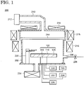
- FIG. 1 a schematic cross-sectional view of the etching apparatus 200 for performing dry etching on a variety of films is shown as an example of a film-processing apparatus.
- the etching apparatus 200 includes a chamber 202 supplying a space for performing etching on films of a conductor, an insulator, a semiconductor, and the like formed over a substrate.
- a gas (also referred to as a gas for cooling) is supplied for cooling a center portion of the stage 100 while using a sheath heater (described below) 124 arranged in the stage 100 as described below.
- the etching apparatus 200 is equipped with a heater power source 222 for controlling the sheath heater 124 and a gas-supplying device 150.
- a cooling device may be connected to the gas-supplying device 150 for cooling the gas for cooling supplied from the gas-supplying device 150.
- FIG. 3A Schematic views of cross sections along chain lines A-A' and B-B' in FIG. 2B are respectively shown in FIG. 3A and FIG. 3B .
- a gas-supplying tube 142 connected to the gas-supplying device 150 is provided in the shaft 140.
- the gas-supplying tube 142 has a hollow structure and is configured so that the gas for cooling supplied from the gas-supplying device 150 flows in the gas-supplying tube 142 and is then supplied in a direction toward the first supporting plate 120.
- a material included in the gas-supplying tube 142 and a metal such as iron, aluminum, copper, an alloy such as stainless steel and brass, or a vinyl polymer such as poly(vinyl chloride) and polyethylene may be used as the material.
- a fluorine-containing polymer such as polytetrafluoroethylene may be used as a vinyl polymer.
Landscapes
- Chemical & Material Sciences (AREA)
- Engineering & Computer Science (AREA)
- Organic Chemistry (AREA)
- Chemical Kinetics & Catalysis (AREA)
- Materials Engineering (AREA)
- Mechanical Engineering (AREA)
- Metallurgy (AREA)
- General Chemical & Material Sciences (AREA)
- Physics & Mathematics (AREA)
- Plasma & Fusion (AREA)
- Analytical Chemistry (AREA)
- Manufacturing & Machinery (AREA)
- Ceramic Engineering (AREA)
- Inorganic Chemistry (AREA)
- Drying Of Semiconductors (AREA)
- Container, Conveyance, Adherence, Positioning, Of Wafer (AREA)
Abstract
Description
- An embodiment of the present invention relates to a stage for supporting a substrate, a film-forming apparatus or a film-processing apparatus including the stage, and a method for controlling the temperature of a substrate.
- A semiconductor device is installed in almost all electronic devices and has a significant role for their functions. A semiconductor device utilizes the semiconductor properties of silicon or the like and is prepared by stacking a variety of patterned semiconductor films, insulating films, and conducting films over a substrate. These films are formed by utilizing an evaporation method, a sputtering method, a chemical vapor deposition (CVD) method, or a chemical reaction of the substrate and are processed (patterned) with a photolithography process.
- The properties of these films are strongly influenced by the conditions when the films are formed or patterned. One of the conditions is the temperature of a substrate. In most cases, a supporting stage (hereinafter, referred to as a stage) for supporting a substrate is controlled so that the temperature thereof is as uniform as possible in order to maintain a uniform temperature throughout the substrate. The temperature control of the stage is carried out by heating a heater provided in the stage and simultaneously flowing a coolant in a channel for a coolant formed in the stage (see, the
Patent Documents 1 and 2). -
- Patent Document 1:
Japanese Patent Application Publication No. 2018-056333 - Patent Document 2:
Japanese Patent Application Publication No. 2014-175491 - An object of an embodiment of the present invention is to provide a stage for precisely controlling a temperature of a substrate. Alternatively, an object of an embodiment of the present invention is to provide a film-forming apparatus or a film-processing apparatus including the stage. Alternatively, an object of an embodiment of the present invention is to provide a method for precisely controlling the temperature of a substrate.
- An embodiment of the present invention is a stage. The stage includes a shaft, a first supporting plate over the shaft, a heater arranged in a trench formed in the first supporting plate, and a gas-supplying tube arranged in the shaft and configured to blow a gas to the first supporting plate
- An embodiment of the present invention is a method for controlling a temperature of a substrate. The method includes arranging a substrate over a stage comprising a first plate and a shaft under the first supporting plate, heating the first stage with a heater arranged in a channel formed in the first supporting plate, and blowing a gas to the first supporting plate from a gas-supplying tube arranged in the shaft.
-
-
FIG. 1 is a schematic cross-sectional view of a film-processing apparatus according to an embodiment of the present invention; -
FIG. 2A is a schematic perspective view of a stage according to an embodiment of the present invention; -
FIG. 2B is a schematic top view of a stage according to an embodiment of the present invention; -
FIG. 3A is a schematic cross-sectional view of a stage according to an embodiment of the present invention; -
FIG. 3B is a schematic top view of a stage according to an embodiment of the present invention; -
FIG. 4A is a schematic cross-sectional view of a stage according to an embodiment of the present invention; -
FIG. 4B is a schematic top view of a stage according to an embodiment of the present invention; -
FIG. 5A is a schematic perspective view of a gas-supplying tube of a stage according to an embodiment of the present invention; -
FIG. 5B is a schematic cross-sectional view of a gas-supplying tube of a stage according to an embodiment of the present invention; -
FIG. 6 is a schematic view showing a temperature distribution of a stage according to an embodiment of the present invention; -
FIG. 7A is a schematic cross-sectional view of a stage according to an embodiment of the present invention; -
FIG. 7B is a schematic cross-sectional view of a stage according to an embodiment of the present invention; -
FIG. 7C is a schematic cross-sectional view of a stage according to an embodiment of the present invention; -
FIG. 8 is a schematic cross-sectional view of a film-forming apparatus according to an embodiment of the present invention; -
FIG. 9 is a schematic cross-sectional view of a film-forming apparatus according to an embodiment of the present invention; -
FIG. 10 is a schematic cross-sectional view of a film-forming apparatus according to an embodiment of the present invention; -
FIG. 11 is a schematic top view of a stage in the example; -
FIG. 12A is a temperature distribution of a first supporting plate in the example; and -
FIG. 12B is a temperature distribution of a first supporting plate in the comparable example. - Hereinafter, each embodiment of the present invention is explained with reference to the drawings. The invention can be implemented in a variety of different modes within its concept and should not be interpreted only within the disclosure of the embodiments exemplified below.
- The drawings may be illustrated so that the width, thickness, shape, and the like are illustrated more schematically compared with those of the actual modes in order to provide a clearer explanation. However, they are only an example, and do not limit the interpretation of the invention. In the specification and the drawings, the same reference number is provided to an element that is the same as that which appears in preceding drawings, and a detailed explanation may be omitted as appropriate.
- In the specification and drawings, the same reference numeral is used when the same or similar structures are collectively expressed, while a small letter is further added thereto when these structures are distinctively expressed. When a plurality of portions in a single structure is distinctively expressed, the same reference number is used, and a hyphen and a natural number are further added.
- In the present embodiment, a
stage 100 according to an embodiment of the present invention and anetching apparatus 200 which is a film-processing apparatus equipped with thestage 100 are explained. - In
FIG. 1 , a schematic cross-sectional view of theetching apparatus 200 for performing dry etching on a variety of films is shown as an example of a film-processing apparatus. Theetching apparatus 200 includes achamber 202 supplying a space for performing etching on films of a conductor, an insulator, a semiconductor, and the like formed over a substrate. - An
exhaust device 204 is connected to thechamber 202 by which the inside of thechamber 202 can be set under a reduced pressure atmosphere. Thechamber 202 is further equipped with aninlet tube 206 for introducing a reaction gas, and the reaction gas for etching is supplied to the chamber through avalve 208. A fluorine-containing organic compound such as tetrafluorocarbon (CF4), octafluorocyclobutane (c-C4F8), decafluorocyclopentane (c-C5F10), and hexafluorobutadiene (C4F6) is represented as the reaction gas for example. - A
microwave source 212 may be disposed at an upper portion of thechamber 202 through awaveguide tube 210. Themicrowave source 212 has an antenna or the like for supplying microwaves and outputs high-frequency microwaves such as a microwave of 2,45 GHz and a radio wave (RF) of 13.56 MHz. The microwaves generated by themicrowave source 212 are transmitted to an upper portion of thechamber 202 by thewaveguide tube 210 and introduced into thechamber 202 through awindow 214 including quartz, ceramics, or the like. The reaction gas is converted to a plasma with the microwaves, and the films are etched with electrons, ions, and radicals included in the plasma. - The
stage 100 according to an embodiment of the present invention is disposed at a lower portion of thechamber 202 for arranging a substrate. The substrate which is not illustrated is arranged over thestage 100. Apower source 220 is connected to thestage 100, and high-frequency electric power is provided to thestage 100 so that an electric field generated by the microwaves is formed on a surface of thestage 100 in a direction perpendicular to a substrate surface.Magnets 216 may be further disposed at an upper portion and on a side surface of thechamber 202. Themagnets 216 may be a permanent magnet or an electromagnet having an electromagnetic coil. A magnetic field component parallel to the surfaces of thestage 100 and the substrate is formed by themagnets 216, and electrons in the plasma receive a Lorentz force to resonate so that they become bound to the surfaces of thestage 100 and the substrate. Accordingly, a high-density plasma can be generated on the substrate surface. - When the temperature of the substrate is controlled in the
etching apparatus 200, a gas (also referred to as a gas for cooling) is supplied for cooling a center portion of thestage 100 while using a sheath heater (described below) 124 arranged in thestage 100 as described below. Hence, theetching apparatus 200 is equipped with aheater power source 222 for controlling thesheath heater 124 and a gas-supplyingdevice 150. Although not illustrated, a cooling device may be connected to the gas-supplyingdevice 150 for cooling the gas for cooling supplied from the gas-supplyingdevice 150. A power source 244 for an electrostatic chuck for fixing the substrate to thestage 100, atemperature controller 226 for performing temperature control of a fluid circulated in thestage 100, and a rotation-controlling device (not illustrated) for rotating thestage 100 may be further connected to thestage 100 as optional components. A mechanism for transporting the substrate may be arranged in thechamber 202. There is no limitation to the mechanism, and atransportation robot 230 equipped with a robot arm may be arranged as shown inFIG. 1 . - A schematic perspective view of the
stage 100 according to an embodiment is shown inFIG. 2A . As shown inFIG. 2A , thestage 100 has ashaft 140 and includes, over theshaft 140, a first supportingplate 120 supported by theshaft 140 and a second supportingplate 110 over the first supporting plate as a fundamental structure. In FIG. 1A, the first supportingplate 120 and the second supportingplate 110 each have a disk shape with a circular top surface. However, the shapes thereof are not limited and may be a shape matching the shape of the employed substrate. For example, the first supportingplate 120 and the second supportingplate 110 each may have a rectangular parallelepiped shape with a rectangular top surface. - A schematic top view of the
stage 100 is shown inFIG. 2B . InFIG. 2B , the second supportingsubstrate 110 is not illustrated. One or a plurality of trenches 122 (seeFIG. 3B ) is formed along the top surface thereof, and asheath heater 124 is arranged in each of thetrenches 122. A heating wire (heating wire) electrically connected to the heater power source 222 (seeFIG. 1 ) is provided in thesheath heater 124. Thesheath heaters 124 are heated by electrical power from theheater power source 222. Thetrenches 122 are formed so that the whole of the supportingplate 120 is uniformly heated with thesheath heaters 124. The heat of the first supportingplate 120 is transmitted to the second supporting plate 112, and the substrate arranged over the second supportingplate 110 is heated with this heat. Although not illustrated, trenches may also be formed in the second supportingplate 110, and thesheath heaters 124 may be accommodated in thetrenches 122 of the first supportingplate 120 and the trenches of the second supportingplate 110. Alternatively, trenches may be formed in the second supportingplate 110 without forming anytrench 122 in the first supportingplate 120 so that thesheath heaters 124 are arranged in the trenches thereof. - The first supporting
plate 120 and the second supportingplate 110 each contain a metal selected from metals having a thermal conductivity equal to or higher than 10 W/mK and equal to or lower than 430 W/mk. The thermal energy generated by thesheath heaters 124 can be efficiently received by using a metal with a high thermal conductivity. In addition, the metal is preferred to have a thermal expansion coefficient equal to or higher than 3×10⁻⁶ /K and equal to or lower than 25×10-6 /K. As a specific metal meeting such characteristics, a metal such as titanium, aluminum, and stainless steel is represented. The metal included in the second supportingplate 110 and the metal included in the first supportingplate 120 may be the same as or different from each other. When they are different from each other, the metals may be selected so that a difference in thermal expansion coefficient between the metals included in the first supportingplate 120 and the second supportingplate 110 is equal to or lower than 250×10-6 /K. This configuration suppresses deformation caused by the thermal expansion, allowing the formation of thestage 100 with high reliability. - The second supporting
plate 110 and the first supportingplate 120 are bonded to each other. The bonding of the first supportingplate 120 and the second supportingplate 110 can be carried out by welding, screw bonding, or brazing. An alloy containing silver, copper, and zinc, an alloy containing copper and zinc, a copper containing a small amount of phosphorus, aluminum or an alloy thereof, an alloy containing titanium, copper, and nickel, an alloy containing titanium, zirconium, and copper, an alloy containing titanium, zirconium, copper, and nickel, and the like are represented as a braze used in brazing. - Schematic views of cross sections along chain lines A-A' and B-B' in
FIG. 2B are respectively shown inFIG. 3A and FIG. 3B . As demonstrated inFIG. 3A , a gas-supplyingtube 142 connected to the gas-supplyingdevice 150 is provided in theshaft 140. The gas-supplyingtube 142 has a hollow structure and is configured so that the gas for cooling supplied from the gas-supplyingdevice 150 flows in the gas-supplyingtube 142 and is then supplied in a direction toward the first supportingplate 120. There is no limitation to a material included in the gas-supplyingtube 142, and a metal such as iron, aluminum, copper, an alloy such as stainless steel and brass, or a vinyl polymer such as poly(vinyl chloride) and polyethylene may be used as the material. A fluorine-containing polymer such as polytetrafluoroethylene may be used as a vinyl polymer. - The gas for cooling supplied through the gas-supplying
tube 142 is used to cool the center portion of the first supportingplate 120 so as to allow the center portion to have a lower temperature than the circumference portion. The gas-supplyingtube 142 is preferred to be disposed so that a center axis thereof passes through the center of the first supportingplate 120. Hence, when the plane shape of the first supportingplate 120 is a circle (that is, when the first supportingplate 120 has a disk shape), it is preferred to provide the gas-supplyingtube 142 so that the center axis thereof passes through the center of the circle. However, the arrangement of the gas-supplyingtube 142 may not be strictly controlled in this way, and the gas-supplyingtube 142 may be arranged so that the center of the first supportingplate 120 and a vicinity thereof can be cooled. Therefore, the gas-supplyingtube 142 may be arranged so that a cross section of the gas-supplyingtube 142 parallel to a top surface of the first supportingplate 120 overlaps the center of the first supportingplate 120, for example. - A distance D (see
FIG. 3A ) between a tip of the gas-supplyingtube 142 and the first supportingplate 120 may be appropriately set in view of the size of the first supportingplate 120, the amount of the supplied gas for cooling, the temperature of the gas for cooling, and the like and may be selected from a range equal to or more than 1 mm and equal to or less than 30 mm, equal to or more than 5 mm and equal to or less than 20 mm, or equal to or more than 5 mm and equal to or less than 15 mm. It is possible to selectively cool the center portion of the first supportingplate 120 while preventing the stream of the gas for cooling from widely diffusing before contacting the first supportingplate 120 by setting the distance D within the aforementioned range. Simultaneously, generation of a large temperature gradient can be avoided around the center portion. - It is preferred that the gas for cooling not be released into the
chamber 202. This is because the gas composition and pressure in thechamber 202 vary due to the gas for cooling. Hence, theshaft 140 and the first supportingplate 120 are preferably configured so that the gas for cooling does not leak into thechamber 202. For example, no through hole is provided to the first supportingplate 120 at least in a region overlapping theshaft 140 to block the gas for cooling. Furthermore, theetching apparatus 200 may be configured to exhaust the gas for cooling by providing one or a plurality of throughholes 202a to thechamber 202 in the region overlapping theshaft 140 as shown inFIG. 3A . With this structure, the gas for cooling supplied in a direction toward the first supportingplate 120 comes in contact with the center of the first supportingplate 120 and then changes in direction in theshaft 140 so as to be exhausted outside thechamber 202 as shown by the dotted line inFIG. 3A . - Air, nitrogen, argon, a mixed gas thereof, and the like can be used as the gas for cooling,, and the temperature thereof may be room temperature or may be appropriately selected from a range equal to or higher than -20 °C or equal to or lower than 30 °C, 0 °C or equal to or lower than 25 °C, or 10 °C or equal to or lower than 25 °C. When a temperature other than room temperature is selected, the temperature of the gas for cooling may be controlled with a cooling device. A flow amount of the gas for cooling is also appropriately adjusted and may be selected from a range equal to or more than 10 L/min and equal to or less than 1000 L/min, 30 L/min and equal to or less than 500 L/min, or 30 L/min and equal to or less than 300 L/min.
- As described above, the
trench 122 is formed at the upper surface of the first supportingplate 120, and thesheath heater 124 is arranged along the trench 122 (FIG. 3B ). There is also no limitation to the structure of thesheath heater 124, and a double-terminal type sheath heater having terminals at both terminals or a single-terminal type sheath heater having two terminals only at one terminal may be used. The heater wiring of thesheath heater 124 is connected to awiring 126 extending in theshaft 140, is extracted to the outside through the throughhole 202a provided to thechamber 202, and is connected to theheater power source 222. - A gas-discharging
tube 144 for controlling the discharge of the gas for cooling may be provided in theshaft 140. For example, one or a plurality of gas-dischargingtubes 144 is inserted into theshaft 140 through the throughholes 202a of thechamber 202 as shown inFIG. 4A . The position of the edge portions of the gas-dischargingtubes 144 may be arbitrarily adjusted, and a distance to the first supportingplate 120 may be the same as the distance D (seeFIG. 3A ) or smaller or larger than the distance D. The gas-dischargingtube 144 may be arranged along an inner wall of theshaft 140 or may be arranged so as to be in contact with the gas-supplyingtube 142 as shown inFIG. 4B . Although not illustrated, the gas for cooling may be sucked up by connecting a gas-exhaust device to the gas-dischargingtubes 144. The stream of the gas for cooling can be more precisely controlled by employing such a structure. - Alternatively, a gas-supplying-discharging tube having an ability to simultaneously supply and discharge the gas for cooling may be used. For example, a gas-supplying-discharging
tube 146 may be employed instead of the gas-supplyingtube 142 and the gas-dischargingtube 144, where the gas-supplying-dischargingtube 146 has a gas-supplyingportion 142a connected to the gas-supplyingdevice 150 and gas-dischargingportions 144a arranged to surround the gas-supplyingportion 142a and integrated with the gas-supplyingportion 142a as shown inFIG. 5A and FIG. 5B . In the gas-supplying-dischargingtube 146, the gas-supplyingportion 142a and the gas-dischargingportions 144a are separated by a single partition wall. The use of the gas-supplying-dischargingtube 146 allows the space in theshaft 140 to be efficiently utilized. Accordingly, the number of independently controlledsheath heaters 124 can be increased, which contributes to more precise control of the temperature of thestage 100. - A stage arranged in the traditional film-processing apparatus or film-forming apparatus is designed so that the whole of the supporting plate has a uniform temperature in order to uniformly heat the whole of the substrate arranged over the stage. That is, the number of sheath heaters, the arrangement thereof, and the like are determined so that the supporting plate has the same temperature throughout from its center portion to the circumference portion as demonstrated by a linear line (c) in a conceptional drawing of
FIG. 6 . However, the heat release from the circumference portion of the stage cannot be ignored in the film-processing apparatus and the film-forming apparatus, and the heat dissipates to thechamber 202 and a mechanism for transporting the substrate such as thetransportation robot 230 described inFIG. 1 as well as pins for moving the substrate in a vertical direction and protection tools (not illustrated) arranged close to the stage. As a result, even if the stage is designed so as to provide an ideal temperature profile represented by the linear line (c) in the case where no heat dissipation occurs, the temperature of the circumference portion of the stage decreases (dotted line (a)) to cause a temperature distribution in the substrate. - In contrast, the gas for cooling is supplied to the center portion of the first supporting
plate 120 while heating the second supportingplate 110 through the first supportingplate 120 using thesheath heaters 124 in thestage 100 according to an embodiment of the present invention. As a result, the temperatures of the first supportingplate 120 and the second supportingplate 110 can be controlled so that the temperature of the center portion is lower than the temperature of the circumference portion as shown by the dotted line (b). Production of such a temperature profile establishes a balance with the heat dissipation from the circumference portions of the first supportingplate 120 and the second supportingplate 110, thereby realizing the ideal temperature profile represented by the linear line (c) or a similar temperature profile. Accordingly, it is possible to process or from a film over a substrate while maintaining a uniform temperature throughout the substrate. - The structure of the
stage 100 is not limited to the aforementioned structure, and a variety of structures may be employed. For example, a trench (channel) 128 for circulating a fluid may be formed on a lower surface of the first supporting plate as shown inFIG. 7A . In this case, a third supportingplate 130 for covering thechannel 128 is provided to thestage 100, and the gas for cooling is blown to the first supportingplate 120 through the third supporting plate. The third supporting plate may include a metal usable for the first supportingplate 120 and the second supportingplate 110. The third supportingplate 130 is fixed to the first supporting plate by welding, screw bonding, or brazing. Although not illustrated, thechannel 128 may be formed in the third supportingplate 130 without forming thechannel 128 in the first supportingplate 120. The temperature of the substrate can be more precisely controlled by flowing a fluid with a temperature controlled by thetemperature controller 226 in thechannel 128. The medium may be used in both cases of cooling and heating thestage 100. A liquid medium such as water, an alcohol such as isopropanol and ethylene glycol, silicon oil, and a fluorine-based fluid such as a fluorocarbon may be used as the medium. - In addition, one or a plurality of
openings 132 may be formed in the first supportingplate 120 and the third supportingplate 130 for arranging a temperature sensor. A thermocouple or the like may be utilized as a temperature sensor. - Alternatively, one or a plurality of through
holes 134 passing through the first supportingplate 120, the second supportingplate 110, and the third supportingplate 130 may be provided as shown inFIG. 7B . A source of a gas having a high thermal conductivity such as helium is connected to the throughhole 134 via a gas-supplyingtube 136. This structure allows a gas having a high thermal conductivity to flow in a gap between the second supportingplate 110 and the substrate, thereby efficiently transferring the thermal energy of thesheath heater 124 to the substrate. Note that the throughhole 134 may be formed so as to overlap theshaft 140 or may be formed in a region which does not overlap theshaft 140 as shown inFIG. 7B . It is possible to prevent the gas for cooling from leaking from the throughhole 134 and diffusing into thechamber 202 and to secure a large space for arranging thewiring 126 and the gas-supplyingtube 142 in theshaft 140 by forming the throughhole 134 so as not to overlap theshaft 140. - Alternatively, an
electrostatic chuck 160 as a mechanism to fix the substrate over thestage 100 may be provided over the first supporting plate as shown inFIG. 7C . Theelectrostatic chuck 160 may have a structure in which anelectrostatic chuck electrode 164 is covered with an insulatingfilm 162. The substrate can be fixed with the Coulomb force between the charge formed in theelectrostatic chuck electrode 164 by applying a high voltage (several hundred volts to several thousand volts) from the power source 244 for an electrostatic chuck (seeFIG. 1 ) to theelectrostatic chuck electrode 164 and the charge generated on the back surface of the substrate and having the opposite polarity to the charge generated on theelectrostatic chuck electrode 164. Ceramics such as aluminum oxide, aluminum nitrate, and boron nitride may be used as an insulator. Note that it is not always necessary for the insulatingfilm 162 to completely have an insulating property, and the insulatingfilm 162 may have a certain degree of conductivity (e.g., resistivity in the order of 109 Ω·cm to 1012 Ω·cm). In this case, the aforementioned ceramics are doped with a metal oxide such as titanium oxide, zirconium oxide, and hafnium oxide in thefilm 162. Arib 166 for determining the position of the substrate may be provided at a circumference of theelectrostatic chuck 160. - As described above, the gas for cooling is supplied from the gas-supplying
tube 142 arranged in theshaft 140 to the center portion of the first supportingplate 120 in thestage 100 according to the present embodiment so that the temperatures of the center portions of the first supportingplate 120 and the second supportingplate 110 are lower than the temperatures of their circumference portions. Accordingly, a good balance is established between the input of heat from thesheath heater 124 and the heat dissipation from the circumference portions, allowing the entire first supportingplate 120 and the second supportingplate 110 to have a uniform temperature, by which the temperature of the whole of the substrate can be uniformly controlled. - In the present embodiment, a variety of film-forming apparatus having the
stage 100 described in the First Embodiment is explained usingFIG. 8 to FIG. 10 . Descriptions of the structures the same as those of the First Embodiment may be omitted. -
FIG. 8 is a schematic view of aCVD apparatus 300 serving as a film-forming apparatus. TheCVD apparatus 300 includes achamber 302 supplying a space for chemically reacting a reaction gas. - An
exhaust device 304 is connected to thechamber 302 by which the pressure in thechamber 302 can be reduced. Thechamber 302 is further provided with aninlet tube 306 for introducing the reaction gas, and the reaction gas for film formation is introduced into the chamber through avalve 308. A variety of gases may be used as the reaction gas depending on the film to be formed. The gas may be a liquid at a normal temperature. For example, the use of silane, dichlorosilane, tetraethoxysilane, or the like allows the formation of a thin film of silicon, silicon oxide, silicon nitride, or the like. Alternatively, a thin film of a metal such as tungsten and aluminum can be formed by using tungsten fluoride, trimethyl aluminum, and the like. - Similar to the
etching apparatus 200, amicrowave source 312 may be disposed at an upper portion of thechamber 302 through awaveguide tube 310. The microwaves generated by themicrowave source 312 are introduced into thechamber 302 by thewaveguide tube 310. The reaction gas is converted to a plasma with the microwaves, and the chemical reactions of the gas are promoted by a variety of active species included in the plasma, by which products obtained by the chemical reactions are deposited over a substrate to provide a thin film. Amagnet 344 may be disposed as an optional component in thechamber 202 for increasing the plasma density. Thestage 100 described in the First Embodiment is arranged at a lower portion of thechamber 302, by which deposition of thin films can be performed in a state where the substrate is disposed over thestage 100. Similar to theetching apparatus 200,magnets chamber 302. - A
power source 320 for supplying high-frequency electric power to thestage 100, aheater power source 322 for controlling thesheath heater 124, apower source 324 for the electrostatic chuck, and atemperature controller 326 for controlling the temperature of the fluid circulated in thestage 100 may be connected to thestage 100. A rotation-controlling device (not illustrated) for rotating thestage 100 may be provided to theCVD apparatus 300 as an optional component. -
FIG. 9 is a schematic view of asputtering apparatus 400 as one of the film- forming apparatuses. The sputtering apparatus has achamber 402 to supply a space for collision of high-speed ions with a target and deposition of the target atoms formed by the collision. - An
exhaust device 400 for reducing the pressure in thechamber 402 is connected to thechamber 402. Aninlet tube 406 and avalve 408 for introducing a sputtering gas such as argon to thechamber 402 is provided to thechamber 402. - A
target stage 410 supporting a target including a material subjected to the film formation and serving as a cathode is arranged at a lower portion of thechamber 402, over which thetarget 412 is disposed. A high-frequency power source 414 is connected to thetarget stage 410, and plasma can be formed in thechamber 402 by the high-frequency power source 414. - The
stage 100 described in the First Embodiment can be disposed at an upper portion of thechamber 402. In this case, thin-film formation proceeds in a state where the substrate is arranged under thestage 100. Similar to theetching apparatus 200 and theCVD apparatus 300, apower source 420 for supplying high-frequency electric power to thestage 100, aheater power source 422, apower source 424 for an electrostatic chuck, and atemperature controller 426 may by connected to thestage 100. A rotation-controlling device (not illustrated) for rotating thestage 100 may be installed in thesputtering device 400 as an optional component. - Argon ions accelerated by the plasma generated in the
chamber 402 collide with thetarget 412, and the atoms of thetarget 412 are sputtered. The sputtered atoms fly to the substrate and are deposited over the substrate arranged under thestage 100 while ashutter 416 is opened. - A structure is exemplified in the present embodiment in which the
stage 100 and thetarget stage 410 are respectively arranged at the upper and lower portions of thechamber 402. However, the present embodiment is not limited to this structure, and thesputtering apparatus 400 may be configured so that the target is located over thestage 100. Alternatively, thetarget stage 410 may be provided so that a main surface of the substrate is arranged perpendicularly to the horizontal plane and that thetarget stage 410 is disposed to oppose thereto. -
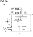
FIG. 10 is a schematic view of anevaporation apparatus 500 as one of the film-forming apparatus. Theevaporation apparatus 500 has achamber 502 to supply a space for evaporating a material in anevaporation source 510 and depositing the evaporated material over a substrate. - An
exhaust device 504 for creating a high vacuum in thechamber 502 is connected to thechamber 502. Aninlet tube 506 for retrieving an atmospheric pressure in thechamber 502 is provided to thechamber 502, and an inert gas such as nitrogen and argon is introduced to thechamber 502 via avalve 508. - The
stage 100 described in the First Embodiment may be disposed at an upper portion of thechamber 502. Deposition of a material proceeds in a state where the substrate is arranged under thestage 100. Similar to theetching apparatus 200, theCVD apparatus 300, thesputtering apparatus 400, aheater power source 522, apower source 524 for an electrostatic chuck, and atemperature controller 526 may be connected to thestage 100. A rotation-controllingdevice 528 for rotating thestage 100 may also be provided as an optional component. Although not illustrated, thestage 100 may further have a mask holder for fixing a metal mask between the substrate and theevaporation source 510, by which the metal mask can be arranged at a vicinity of the substrate so that opening portions of the metal mask overlap with the regions for depositing the material. - The
evaporation source 510 is disposed at a lower portion of the chamber, and the material to be evaporated is charged in theevaporation source 510. A heater is provided to theevaporation source 510 for heating the material and is controlled with acontrolling device 510. The inside of thechamber 502 is set to a highly vacuum state with theexhaust device 504, and the material is vaporized by heating theevaporation source 510 so that the evaporation starts. The deposition of the material starts on the substrate by opening ashutter 514 when the evaporation rate becomes constant. - As described above, the film-forming apparatus such as the
CVD apparatus 300, thesputtering apparatus 400, and the evaporation source according to the present embodiment may include thestage 100 explained in theEmbodiment 1. Hence, the temperature of the substrate can be precisely controlled and adjusted with high responsiveness, which facilitates the control of the physical properties of the thin films to be produced. - In this example, the results for measuring a temperature profile of the
stage 100 described in the First Embodiment are described. - In this Example, the stage 100 (see
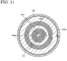
FIG. 2A ) including the first supportingplate 120 and the second supportingplate 110 made of aluminum was used. As shown inFIG. 11 , three sheath heaters (first sheath heater 124a, asecond sheath heater 124b, and athird sheath heater 124c (each have an outer diameter of 310 mm and a capacitance of 1200 W)) were arranged in the first supportingplate 120. Thefirst sheath heater 124a was arranged so as to overlap theshaft 140 and surround a region overlapping the gas-supplyingtube 142 several times. Thesecond sheath heater 124b wound approximately three times to surround thefirst heater 124a was arranged. Thethird sheath heater 124c was arranged closest to the circumference portion of the first supportingplate 120. A total thickness of the first supportingplate 120 and the second supportingplate 110 was 33 mm, and the diameters thereof were each 322 mm. Three thermocouples were arranged in the first supportingplate 120 and the second supportingplate 110, and heating was carried out by applying a current to these threesheath heaters 124. The heating was carried out to apply a current to eachsheath heater 124 using a power source of 200 V and 10 A so that the temperature increases to a predetermined temperature under the PID control. Air at room temperature was used as the gas for cooling and supplied to the center portion of the first supportingplate 120 via the gas-supplyingtube 142 at a flow rate of 100 L/min. - The heating was carried out in a state where a dummy wafer was disposed on a surface of the second supporting
plate 110, and then temperatures were measured at 17 points after the temperature reached a steady state. A drawing schematically representing the temperature distribution is illustrated inFIG. 12A on the basis of the results. As can be understood fromFIG. 12A , the temperature at the center portion of the second supportingplate 110 is lower than that of the circumference portion thereof. Specifically, the temperatures of the center portion A and the circumference portion B were 145.2 °C and 155 °C, respectively, and the difference therebetween was 9.8 °C. - A schematic drawing of the temperature distribution obtained by conducting a similar experiment without supplying the gas for cooling is shown in
FIG. 12B . As can be understood from this drawing, the temperature was uniform across the second supportingplate 110 in the case where the gas for cooling was not supplied. The temperatures of the center portion A and the circumference portion B were 152.4 °C and 155 °C, respectively, and the difference therebetween was 2.6 °C. - From these results, it has been proven that the temperatures of the center portions of the first supporting
plate 120 and the second supportingplate 110 can be set to be lower than the temperature of the circumference portion by supplying the gas for cooling in thestage 100 according to one of the embodiments. When thestage 100 is used in a film-forming apparatus and a film-processing apparatus, heat dissipation occurs from the circumference portion. Hence, it was confirmed that the use of thestage 100 according to one of the embodiments realizes an ideal temperature profile and allows the temperature of a substrate to be uniformly controlled across the substrate. - The aforementioned modes described as the embodiments of the present invention can be implemented by appropriately combining with each other as long as no contradiction is caused. Furthermore, any mode which is realized by persons ordinarily skilled in the art through the appropriate addition, deletion, or design change of elements or through the addition, deletion, or condition change of a process is included in the scope of the present invention as long as they possess the concept of the present invention.
- It is understood that another effect different from that provided by the modes of the aforementioned embodiments is achieved by the present invention if the effect is obvious from the description in the specification or readily conceived by persons ordinarily skilled in the art.
- 100: Stage, 110: Second supporting plate, 120: First supporting plate, 122: Trench, 124: Sheath heater, 124a: First sheath heater, 124b: Second sheath heater, 124c: Third sheath heater, 126: Wiring, 128: Channel, 130:Third supporting plate, 132: Opening, 134: Through hole, 136: Gas-supplying tube, 140: Shaft, 142: Gas-supplying tube, 142a: Gas-supplying portion, 144: Gas-discharging tube, 144a: Gas-discharging portion, 146: Gas-supplying-discharging tube, 150: Gas-supplying device, 160: Electrostatic chuck, 162: Film, 164: Electrostatic chuck electrode, 166: Rib, 200: Etching apparatus, 202: Chamber, 202a: Through hole, 204: Exhaust device, 206: Inlet tube, 208: Valve, 210: Waveguide tube, 212: Microwave source, 214: Window, 216: Magnet, 220: Power source, 222: Heater power source, 224: Power source for an electrostatic chuck, 226: Temperature controller, 230: Transportation robot, 300:CVD apparatus, 302: Chamber, 304: Exhaust device, 306: Inlet tube, 308: Valve, 310: Waveguide tube, 312: Microwave source, 316: Magnet, 318: Magnet, 320: Power source, 322: Heater power source, 324: Power source for an electrostatic chuck, 326: Temperature controller, 344: Magnet, 400: Sputtering apparatus 402: Chamber, 404: Exhaust device, 406: Inlet tube, 408: Valve, 410:Target stage, 412: Target, 414: High-frequency power source, 416: Shutter, 420: Power source, 422: Heater power source, 424: Power source for an electrostatic chuck, 426: Temperature controller, 500: Evaporation apparatus, 502: Chamber, 504: Exhaust device, 506: Inlet tube, 508: Valve, 510: Evaporation source, 512: Controlling device, 514: Shutter, 522: Heater power source, 524: Power source for an electrostatic chuck, 526: Temperature controller, 528: Rotation-controlling device
Claims (12)
- A stage comprising:a shaft;a first supporting plate over the shaft;a heater arranged in a trench formed in the first supporting plate; anda gas-supplying tube arranged in the shaft and configured to blow a gas to the first supporting plate.
- The stage according to claim 1,wherein the first supporting plate has a disk shape, andwherein a cross section of the gas-supplying tube parallel to a surface of the first supporting plate overlaps a center of the disk shape.
- The stage according to claim 1,
wherein the first supporting plate is configured to block the gas and not to release the gas into a chamber in which the stage is arranged. - The stage according to claim 1, further comprising a second supporting plate over the first supporting plate.
- The stage according to claim 1, further comprising a third supporting plate under the first supporting plate,
wherein the first supporting plate has a channel for circulating a fluid. - The stage according to claim 1,
wherein the first plate has a through hole which does not overlap the shaft. - The stage according to claim 1, further comprising a plurality of gas-discharging tubes surrounding the gas-supplying tube.
- A substrate-temperature controlling method, the method comprising:arranging a substrate over a first stage comprising a first supporting plate and a shaft under the first supporting plate;heating the first stage with a heater arranged in a trench formed in the first supporting plate; andblowing a gas to the first supporting plate from a gas-supplying tube arranged in the shaft.
- The substrate-temperature controlling method according to claim 8,wherein the first supporting plate has a disk shape, andwherein the gas is blown so that a temperature of a center of the first supporting plate is lower than a temperature of a circumference portion of the first supporting plate.
- The substrate-temperature controlling method according to claim 8,wherein the first supporting plate has a disk shape, andwherein the gas-supplying tube is arranged so that a cross section of the gas-supplying tube parallel to a surface of the first supporting plate overlaps a center of the disk shape.
- The substrate-temperature controlling method according to claim 8, further comprising discharging the gas to the outside of a chamber in which the stage is arranged so that the gas is not released into the chamber.
- The substrate-temperature controlling method according to claim 8, further comprising flowing a fluid in a channel formed in the first supporting plate.
Applications Claiming Priority (2)
| Application Number | Priority Date | Filing Date | Title |
|---|---|---|---|
| JP2019143756A JP6845286B2 (en) | 2019-08-05 | 2019-08-05 | A stage, a film forming apparatus or film processing apparatus provided with a stage, and a temperature control method for a substrate |
| PCT/JP2020/028804 WO2021024844A1 (en) | 2019-08-05 | 2020-07-28 | Stage and method for controlling temperature of substrate |
Publications (2)
| Publication Number | Publication Date |
|---|---|
| EP4012752A1 true EP4012752A1 (en) | 2022-06-15 |
| EP4012752A4 EP4012752A4 (en) | 2023-08-02 |
Family
ID=74503578
Family Applications (1)
| Application Number | Title | Priority Date | Filing Date |
|---|---|---|---|
| EP20850947.1A Pending EP4012752A4 (en) | 2019-08-05 | 2020-07-28 | PLATE AND METHOD FOR CONTROLLING THE TEMPERATURE OF A SUBSTRATE |
Country Status (7)
| Country | Link |
|---|---|
| US (1) | US12424421B2 (en) |
| EP (1) | EP4012752A4 (en) |
| JP (1) | JP6845286B2 (en) |
| KR (1) | KR102951140B1 (en) |
| CN (1) | CN114097068B (en) |
| TW (1) | TWI772851B (en) |
| WO (1) | WO2021024844A1 (en) |
Families Citing this family (6)
| Publication number | Priority date | Publication date | Assignee | Title |
|---|---|---|---|---|
| US12074055B2 (en) * | 2021-02-25 | 2024-08-27 | Shibaura Mechatronics Corporation | Substrate treatment device |
| JP7316393B2 (en) * | 2021-02-25 | 2023-07-27 | 芝浦メカトロニクス株式会社 | Substrate processing equipment |
| JP2024051768A (en) * | 2022-09-30 | 2024-04-11 | 日本発條株式会社 | stage |
| JP2024051933A (en) * | 2022-09-30 | 2024-04-11 | 日本発條株式会社 | stage |
| KR102650161B1 (en) * | 2023-01-05 | 2024-03-22 | 주식회사 미코세라믹스 | Ceramic susceptor |
| CN116752124B (en) * | 2023-05-17 | 2025-12-02 | 中国电子科技集团公司第四十八研究所 | A method for heating and coating a high-temperature substrate and substrate |
Family Cites Families (23)
| Publication number | Priority date | Publication date | Assignee | Title |
|---|---|---|---|---|
| US6583638B2 (en) * | 1999-01-26 | 2003-06-24 | Trio-Tech International | Temperature-controlled semiconductor wafer chuck system |
| JP3921143B2 (en) * | 2002-07-29 | 2007-05-30 | 京セラ株式会社 | Wafer heating device |
| KR20060069251A (en) * | 2004-12-16 | 2006-06-21 | 주성엔지니어링(주) | Warp Susceptor |
| US20060130764A1 (en) | 2004-12-16 | 2006-06-22 | Jusung Engineering Co., Ltd. | Susceptor for apparatus fabricating thin film |
| US7429718B2 (en) | 2005-08-02 | 2008-09-30 | Applied Materials, Inc. | Heating and cooling of substrate support |
| US20080035306A1 (en) * | 2006-08-08 | 2008-02-14 | White John M | Heating and cooling of substrate support |
| US20080226838A1 (en) | 2007-03-12 | 2008-09-18 | Kochi Industrial Promotion Center | Plasma CVD apparatus and film deposition method |
| JP4558755B2 (en) * | 2007-03-20 | 2010-10-06 | 財団法人高知県産業振興センター | Plasma CVD equipment |
| JP2009049061A (en) * | 2007-08-14 | 2009-03-05 | Sumitomo Electric Ind Ltd | Semiconductor wafer processing apparatus and semiconductor wafer processing method |
| JP2009084686A (en) * | 2007-09-11 | 2009-04-23 | Tokyo Electron Ltd | Substrate mounting mechanism, substrate processing apparatus, method for suppressing film deposition on substrate mounting mechanism, and storage medium |
| JP5222442B2 (en) | 2008-02-06 | 2013-06-26 | 東京エレクトロン株式会社 | Substrate mounting table, substrate processing apparatus, and temperature control method for substrate to be processed |
| JP5341706B2 (en) * | 2009-10-16 | 2013-11-13 | 株式会社ニューフレアテクノロジー | Semiconductor manufacturing apparatus and semiconductor manufacturing method |
| JP5600479B2 (en) * | 2010-06-02 | 2014-10-01 | 助川電気工業株式会社 | Sheath heater lead wire connection terminal |
| DE102012205616B4 (en) | 2012-04-04 | 2016-07-14 | Siltronic Ag | Device for depositing a layer on a semiconductor wafer by means of vapor deposition |
| JP5740372B2 (en) | 2012-09-12 | 2015-06-24 | 株式会社東芝 | Semiconductor memory card |
| JP5980147B2 (en) | 2013-03-08 | 2016-08-31 | 日本発條株式会社 | Substrate support device |
| US8916902B2 (en) | 2013-04-17 | 2014-12-23 | Ubleds Co., Ltd. | LED module packaging structure with an IC chip |
| DE102013104840A1 (en) | 2013-05-10 | 2014-11-13 | Osram Opto Semiconductors Gmbh | Radiation-emitting semiconductor component and method for producing radiation-emitting semiconductor components |
| JP6374301B2 (en) | 2013-12-24 | 2018-08-15 | 東京エレクトロン株式会社 | Stage, stage manufacturing method, heat exchanger |
| JP2018056333A (en) | 2016-09-29 | 2018-04-05 | 日本発條株式会社 | Substrate mounting base and manufacturing method therefor |
| JP6615153B2 (en) * | 2017-06-16 | 2019-12-04 | 東京エレクトロン株式会社 | Substrate processing apparatus, substrate mounting mechanism, and substrate processing method |
| DE102017123413B4 (en) | 2017-10-09 | 2023-09-14 | Osram Gmbh | Optoelectronic semiconductor component and manufacturing method for an optoelectronic semiconductor component |
| KR102441541B1 (en) * | 2017-11-09 | 2022-09-08 | 주식회사 미코세라믹스 | Mount, heater having the mount, and deposition apparatus having the heater |
-
2019
- 2019-08-05 JP JP2019143756A patent/JP6845286B2/en active Active
-
2020
- 2020-07-28 KR KR1020227005051A patent/KR102951140B1/en active Active
- 2020-07-28 WO PCT/JP2020/028804 patent/WO2021024844A1/en not_active Ceased
- 2020-07-28 EP EP20850947.1A patent/EP4012752A4/en active Pending
- 2020-07-28 CN CN202080049779.XA patent/CN114097068B/en active Active
- 2020-08-05 TW TW109126414A patent/TWI772851B/en active
-
2022
- 2022-02-04 US US17/592,766 patent/US12424421B2/en active Active
Also Published As
| Publication number | Publication date |
|---|---|
| TW202121577A (en) | 2021-06-01 |
| US20220157579A1 (en) | 2022-05-19 |
| WO2021024844A1 (en) | 2021-02-11 |
| US12424421B2 (en) | 2025-09-23 |
| CN114097068B (en) | 2026-02-27 |
| JP6845286B2 (en) | 2021-03-17 |
| EP4012752A4 (en) | 2023-08-02 |
| KR20220034217A (en) | 2022-03-17 |
| CN114097068A (en) | 2022-02-25 |
| TWI772851B (en) | 2022-08-01 |
| KR102951140B1 (en) | 2026-04-10 |
| JP2021027161A (en) | 2021-02-22 |
Similar Documents
| Publication | Publication Date | Title |
|---|---|---|
| US12424421B2 (en) | Apparatus and method for controlling a substrate temperature | |
| US11201040B2 (en) | Substrate supporting unit and film forming device having the substrate supporting unit | |
| US11862436B2 (en) | Plasma processing apparatus and plasma processing method | |
| US12284731B2 (en) | Heater and stage having the heater | |
| EP3522208A1 (en) | Substrate placement stage, and substrate placement stage fabrication method | |
| US20220151031A1 (en) | Heater | |
| Okumura | Inductively coupled plasma sources and applications | |
| WO2016126425A1 (en) | Low temperature chuck for plasma processing systems | |
| US11424104B2 (en) | Plasma reactor with electrode filaments extending from ceiling | |
| US20210217638A1 (en) | Stage, film-forming apparatus, and film-processing apparatus | |
| WO2010146961A1 (en) | Plasma processing device and cooling device for plasma processing devices | |
| US20050022736A1 (en) | Method for balancing return currents in plasma processing apparatus | |
| EP3866565B1 (en) | Stage, film forming device, and film processing device | |
| US20230207286A1 (en) | Stage and manufacturing method thereof | |
| KR20250037553A (en) | Stage |
Legal Events
| Date | Code | Title | Description |
|---|---|---|---|
| STAA | Information on the status of an ep patent application or granted ep patent |
Free format text: STATUS: THE INTERNATIONAL PUBLICATION HAS BEEN MADE |
|
| PUAI | Public reference made under article 153(3) epc to a published international application that has entered the european phase |
Free format text: ORIGINAL CODE: 0009012 |
|
| STAA | Information on the status of an ep patent application or granted ep patent |
Free format text: STATUS: REQUEST FOR EXAMINATION WAS MADE |
|
| 17P | Request for examination filed |
Effective date: 20220217 |
|
| AK | Designated contracting states |
Kind code of ref document: A1 Designated state(s): AL AT BE BG CH CY CZ DE DK EE ES FI FR GB GR HR HU IE IS IT LI LT LU LV MC MK MT NL NO PL PT RO RS SE SI SK SM TR |
|
| DAV | Request for validation of the european patent (deleted) | ||
| DAX | Request for extension of the european patent (deleted) | ||
| A4 | Supplementary search report drawn up and despatched |
Effective date: 20230704 |
|
| RIC1 | Information provided on ipc code assigned before grant |
Ipc: H05B 3/30 20060101ALI20230628BHEP Ipc: H05B 1/02 20060101ALI20230628BHEP Ipc: H01J 37/32 20060101ALI20230628BHEP Ipc: C23C 14/50 20060101ALI20230628BHEP Ipc: H01L 21/677 20060101ALI20230628BHEP Ipc: C23C 16/46 20060101ALI20230628BHEP Ipc: C23C 16/458 20060101ALI20230628BHEP Ipc: C23C 14/54 20060101ALI20230628BHEP Ipc: H01L 21/687 20060101ALI20230628BHEP Ipc: H01L 21/67 20060101ALI20230628BHEP Ipc: H01L 21/683 20060101ALI20230628BHEP Ipc: H01L 21/3065 20060101AFI20230628BHEP |
|
| REG | Reference to a national code |
Ref country code: DE Ref legal event code: R079 Free format text: PREVIOUS MAIN CLASS: H01L0021306500 Ipc: H10P0072000000 |
|
| GRAP | Despatch of communication of intention to grant a patent |
Free format text: ORIGINAL CODE: EPIDOSNIGR1 |
|
| STAA | Information on the status of an ep patent application or granted ep patent |
Free format text: STATUS: GRANT OF PATENT IS INTENDED |
|
| RIC1 | Information provided on ipc code assigned before grant |
Ipc: H10P 72/00 20260101AFI20260309BHEP Ipc: H10P 72/30 20260101ALI20260309BHEP Ipc: H10P 72/72 20260101ALI20260309BHEP Ipc: H10P 72/76 20260101ALI20260309BHEP Ipc: H05B 3/00 20060101ALI20260309BHEP Ipc: H05B 1/02 20060101ALI20260309BHEP Ipc: H01J 37/32 20060101ALI20260309BHEP Ipc: C23C 14/50 20060101ALI20260309BHEP Ipc: C23C 16/40 20060101ALI20260309BHEP Ipc: C23C 14/54 20060101ALI20260309BHEP Ipc: C23C 16/458 20060101ALI20260309BHEP Ipc: C23C 16/46 20060101ALI20260309BHEP Ipc: H05B 3/30 20060101ALI20260309BHEP |
|
| INTG | Intention to grant announced |
Effective date: 20260324 |
|
| RIN1 | Information on inventor provided before grant (corrected) |
Inventor name: KIDA, NAOYA Inventor name: TATSUMI, ARATA Inventor name: SEKIYA, KENJI Inventor name: AIKAWA, NAOYA Inventor name: TAKANASHI, MASAYA |