EP4011494A1 - Micro-nanofluidic chip, preparation method therefor and use thereof - Google Patents
Micro-nanofluidic chip, preparation method therefor and use thereof Download PDFInfo
- Publication number
- EP4011494A1 EP4011494A1 EP19955997.2A EP19955997A EP4011494A1 EP 4011494 A1 EP4011494 A1 EP 4011494A1 EP 19955997 A EP19955997 A EP 19955997A EP 4011494 A1 EP4011494 A1 EP 4011494A1
- Authority
- EP
- European Patent Office
- Prior art keywords
- microchannel
- inlet
- outlet
- substrate
- nanochannel
- Prior art date
- Legal status (The legal status is an assumption and is not a legal conclusion. Google has not performed a legal analysis and makes no representation as to the accuracy of the status listed.)
- Granted
Links
Images






Classifications
-
- A—HUMAN NECESSITIES
- A61—MEDICAL OR VETERINARY SCIENCE; HYGIENE
- A61K—PREPARATIONS FOR MEDICAL, DENTAL OR TOILETRY PURPOSES
- A61K9/00—Medicinal preparations characterised by special physical form
- A61K9/0087—Galenical forms not covered by A61K9/02 - A61K9/7023
- A61K9/0097—Medicinal compositions released by microdevices, e.g. microelectromechanical systems [MEMS], microdevices comprising chips or microdevices on silicon
-
- B—PERFORMING OPERATIONS; TRANSPORTING
- B01—PHYSICAL OR CHEMICAL PROCESSES OR APPARATUS IN GENERAL
- B01L—CHEMICAL OR PHYSICAL LABORATORY APPARATUS FOR GENERAL USE
- B01L3/00—Containers or dishes for laboratory use, e.g. laboratory glassware; Droppers
- B01L3/50—Containers for the purpose of retaining a material to be analysed, e.g. test tubes
- B01L3/502—Containers for the purpose of retaining a material to be analysed, e.g. test tubes with fluid transport, e.g. in multi-compartment structures
- B01L3/5027—Containers for the purpose of retaining a material to be analysed, e.g. test tubes with fluid transport, e.g. in multi-compartment structures by integrated microfluidic structures, i.e. dimensions of channels and chambers are such that surface tension forces are important, e.g. lab-on-a-chip
- B01L3/502753—Containers for the purpose of retaining a material to be analysed, e.g. test tubes with fluid transport, e.g. in multi-compartment structures by integrated microfluidic structures, i.e. dimensions of channels and chambers are such that surface tension forces are important, e.g. lab-on-a-chip characterised by bulk separation arrangements on lab-on-a-chip devices, e.g. for filtration or centrifugation
-
- A—HUMAN NECESSITIES
- A61—MEDICAL OR VETERINARY SCIENCE; HYGIENE
- A61K—PREPARATIONS FOR MEDICAL, DENTAL OR TOILETRY PURPOSES
- A61K45/00—Medicinal preparations containing active ingredients not provided for in groups A61K31/00 - A61K41/00
- A61K45/06—Mixtures of active ingredients without chemical characterisation, e.g. antiphlogistics and cardiaca
-
- B—PERFORMING OPERATIONS; TRANSPORTING
- B01—PHYSICAL OR CHEMICAL PROCESSES OR APPARATUS IN GENERAL
- B01L—CHEMICAL OR PHYSICAL LABORATORY APPARATUS FOR GENERAL USE
- B01L3/00—Containers or dishes for laboratory use, e.g. laboratory glassware; Droppers
- B01L3/50—Containers for the purpose of retaining a material to be analysed, e.g. test tubes
- B01L3/502—Containers for the purpose of retaining a material to be analysed, e.g. test tubes with fluid transport, e.g. in multi-compartment structures
- B01L3/5027—Containers for the purpose of retaining a material to be analysed, e.g. test tubes with fluid transport, e.g. in multi-compartment structures by integrated microfluidic structures, i.e. dimensions of channels and chambers are such that surface tension forces are important, e.g. lab-on-a-chip
- B01L3/502707—Containers for the purpose of retaining a material to be analysed, e.g. test tubes with fluid transport, e.g. in multi-compartment structures by integrated microfluidic structures, i.e. dimensions of channels and chambers are such that surface tension forces are important, e.g. lab-on-a-chip characterised by the manufacture of the container or its components
-
- B—PERFORMING OPERATIONS; TRANSPORTING
- B01—PHYSICAL OR CHEMICAL PROCESSES OR APPARATUS IN GENERAL
- B01L—CHEMICAL OR PHYSICAL LABORATORY APPARATUS FOR GENERAL USE
- B01L3/00—Containers or dishes for laboratory use, e.g. laboratory glassware; Droppers
- B01L3/50—Containers for the purpose of retaining a material to be analysed, e.g. test tubes
- B01L3/502—Containers for the purpose of retaining a material to be analysed, e.g. test tubes with fluid transport, e.g. in multi-compartment structures
- B01L3/5027—Containers for the purpose of retaining a material to be analysed, e.g. test tubes with fluid transport, e.g. in multi-compartment structures by integrated microfluidic structures, i.e. dimensions of channels and chambers are such that surface tension forces are important, e.g. lab-on-a-chip
- B01L3/502746—Containers for the purpose of retaining a material to be analysed, e.g. test tubes with fluid transport, e.g. in multi-compartment structures by integrated microfluidic structures, i.e. dimensions of channels and chambers are such that surface tension forces are important, e.g. lab-on-a-chip characterised by the means for controlling flow resistance, e.g. flow controllers, baffles or throttle valves
-
- B—PERFORMING OPERATIONS; TRANSPORTING
- B01—PHYSICAL OR CHEMICAL PROCESSES OR APPARATUS IN GENERAL
- B01L—CHEMICAL OR PHYSICAL LABORATORY APPARATUS FOR GENERAL USE
- B01L3/00—Containers or dishes for laboratory use, e.g. laboratory glassware; Droppers
- B01L3/50—Containers for the purpose of retaining a material to be analysed, e.g. test tubes
- B01L3/502—Containers for the purpose of retaining a material to be analysed, e.g. test tubes with fluid transport, e.g. in multi-compartment structures
- B01L3/5027—Containers for the purpose of retaining a material to be analysed, e.g. test tubes with fluid transport, e.g. in multi-compartment structures by integrated microfluidic structures, i.e. dimensions of channels and chambers are such that surface tension forces are important, e.g. lab-on-a-chip
- B01L3/502761—Containers for the purpose of retaining a material to be analysed, e.g. test tubes with fluid transport, e.g. in multi-compartment structures by integrated microfluidic structures, i.e. dimensions of channels and chambers are such that surface tension forces are important, e.g. lab-on-a-chip specially adapted for handling suspended solids or molecules independently from the bulk fluid flow, e.g. for trapping or sorting beads or physically stretching molecules
-
- G—PHYSICS
- G03—PHOTOGRAPHY; CINEMATOGRAPHY; ANALOGOUS TECHNIQUES USING WAVES OTHER THAN OPTICAL WAVES; ELECTROGRAPHY; HOLOGRAPHY
- G03F—PHOTOMECHANICAL PRODUCTION OF TEXTURED OR PATTERNED SURFACES, e.g. FOR PRINTING, FOR PROCESSING OF SEMICONDUCTOR DEVICES; MATERIALS THEREFOR; ORIGINALS THEREFOR; APPARATUS SPECIALLY ADAPTED THEREFOR
- G03F7/00—Photomechanical, e.g. photolithographic, production of textured or patterned surfaces, e.g. printing surfaces; Materials therefor, e.g. comprising photoresists; Apparatus specially adapted therefor
- G03F7/004—Photosensitive materials
- G03F7/038—Macromolecular compounds which are rendered insoluble or differentially wettable
- G03F7/0382—Macromolecular compounds which are rendered insoluble or differentially wettable the macromolecular compound being present in a chemically amplified negative photoresist composition
-
- G—PHYSICS
- G03—PHOTOGRAPHY; CINEMATOGRAPHY; ANALOGOUS TECHNIQUES USING WAVES OTHER THAN OPTICAL WAVES; ELECTROGRAPHY; HOLOGRAPHY
- G03F—PHOTOMECHANICAL PRODUCTION OF TEXTURED OR PATTERNED SURFACES, e.g. FOR PRINTING, FOR PROCESSING OF SEMICONDUCTOR DEVICES; MATERIALS THEREFOR; ORIGINALS THEREFOR; APPARATUS SPECIALLY ADAPTED THEREFOR
- G03F7/00—Photomechanical, e.g. photolithographic, production of textured or patterned surfaces, e.g. printing surfaces; Materials therefor, e.g. comprising photoresists; Apparatus specially adapted therefor
- G03F7/004—Photosensitive materials
- G03F7/039—Macromolecular compounds which are photodegradable, e.g. positive electron resists
- G03F7/0392—Macromolecular compounds which are photodegradable, e.g. positive electron resists the macromolecular compound being present in a chemically amplified positive photoresist composition
-
- G—PHYSICS
- G03—PHOTOGRAPHY; CINEMATOGRAPHY; ANALOGOUS TECHNIQUES USING WAVES OTHER THAN OPTICAL WAVES; ELECTROGRAPHY; HOLOGRAPHY
- G03F—PHOTOMECHANICAL PRODUCTION OF TEXTURED OR PATTERNED SURFACES, e.g. FOR PRINTING, FOR PROCESSING OF SEMICONDUCTOR DEVICES; MATERIALS THEREFOR; ORIGINALS THEREFOR; APPARATUS SPECIALLY ADAPTED THEREFOR
- G03F7/00—Photomechanical, e.g. photolithographic, production of textured or patterned surfaces, e.g. printing surfaces; Materials therefor, e.g. comprising photoresists; Apparatus specially adapted therefor
- G03F7/20—Exposure; Apparatus therefor
-
- G—PHYSICS
- G03—PHOTOGRAPHY; CINEMATOGRAPHY; ANALOGOUS TECHNIQUES USING WAVES OTHER THAN OPTICAL WAVES; ELECTROGRAPHY; HOLOGRAPHY
- G03F—PHOTOMECHANICAL PRODUCTION OF TEXTURED OR PATTERNED SURFACES, e.g. FOR PRINTING, FOR PROCESSING OF SEMICONDUCTOR DEVICES; MATERIALS THEREFOR; ORIGINALS THEREFOR; APPARATUS SPECIALLY ADAPTED THEREFOR
- G03F7/00—Photomechanical, e.g. photolithographic, production of textured or patterned surfaces, e.g. printing surfaces; Materials therefor, e.g. comprising photoresists; Apparatus specially adapted therefor
- G03F7/26—Processing photosensitive materials; Apparatus therefor
- G03F7/30—Imagewise removal using liquid means
- G03F7/32—Liquid compositions therefor, e.g. developers
-
- G—PHYSICS
- G03—PHOTOGRAPHY; CINEMATOGRAPHY; ANALOGOUS TECHNIQUES USING WAVES OTHER THAN OPTICAL WAVES; ELECTROGRAPHY; HOLOGRAPHY
- G03F—PHOTOMECHANICAL PRODUCTION OF TEXTURED OR PATTERNED SURFACES, e.g. FOR PRINTING, FOR PROCESSING OF SEMICONDUCTOR DEVICES; MATERIALS THEREFOR; ORIGINALS THEREFOR; APPARATUS SPECIALLY ADAPTED THEREFOR
- G03F7/00—Photomechanical, e.g. photolithographic, production of textured or patterned surfaces, e.g. printing surfaces; Materials therefor, e.g. comprising photoresists; Apparatus specially adapted therefor
- G03F7/26—Processing photosensitive materials; Apparatus therefor
- G03F7/38—Treatment before imagewise removal, e.g. prebaking
-
- G—PHYSICS
- G03—PHOTOGRAPHY; CINEMATOGRAPHY; ANALOGOUS TECHNIQUES USING WAVES OTHER THAN OPTICAL WAVES; ELECTROGRAPHY; HOLOGRAPHY
- G03F—PHOTOMECHANICAL PRODUCTION OF TEXTURED OR PATTERNED SURFACES, e.g. FOR PRINTING, FOR PROCESSING OF SEMICONDUCTOR DEVICES; MATERIALS THEREFOR; ORIGINALS THEREFOR; APPARATUS SPECIALLY ADAPTED THEREFOR
- G03F7/00—Photomechanical, e.g. photolithographic, production of textured or patterned surfaces, e.g. printing surfaces; Materials therefor, e.g. comprising photoresists; Apparatus specially adapted therefor
- G03F7/26—Processing photosensitive materials; Apparatus therefor
- G03F7/40—Treatment after imagewise removal, e.g. baking
-
- B—PERFORMING OPERATIONS; TRANSPORTING
- B01—PHYSICAL OR CHEMICAL PROCESSES OR APPARATUS IN GENERAL
- B01L—CHEMICAL OR PHYSICAL LABORATORY APPARATUS FOR GENERAL USE
- B01L2200/00—Solutions for specific problems relating to chemical or physical laboratory apparatus
- B01L2200/06—Fluid handling related problems
- B01L2200/0647—Handling flowable solids, e.g. microscopic beads, cells, particles
-
- B—PERFORMING OPERATIONS; TRANSPORTING
- B01—PHYSICAL OR CHEMICAL PROCESSES OR APPARATUS IN GENERAL
- B01L—CHEMICAL OR PHYSICAL LABORATORY APPARATUS FOR GENERAL USE
- B01L2200/00—Solutions for specific problems relating to chemical or physical laboratory apparatus
- B01L2200/12—Specific details about manufacturing devices
-
- B—PERFORMING OPERATIONS; TRANSPORTING
- B01—PHYSICAL OR CHEMICAL PROCESSES OR APPARATUS IN GENERAL
- B01L—CHEMICAL OR PHYSICAL LABORATORY APPARATUS FOR GENERAL USE
- B01L2300/00—Additional constructional details
- B01L2300/08—Geometry, shape and general structure
- B01L2300/0809—Geometry, shape and general structure rectangular shaped
- B01L2300/0819—Microarrays; Biochips
-
- B—PERFORMING OPERATIONS; TRANSPORTING
- B01—PHYSICAL OR CHEMICAL PROCESSES OR APPARATUS IN GENERAL
- B01L—CHEMICAL OR PHYSICAL LABORATORY APPARATUS FOR GENERAL USE
- B01L2300/00—Additional constructional details
- B01L2300/08—Geometry, shape and general structure
- B01L2300/0861—Configuration of multiple channels and/or chambers in a single devices
- B01L2300/0867—Multiple inlets and one sample wells, e.g. mixing, dilution
-
- B—PERFORMING OPERATIONS; TRANSPORTING
- B01—PHYSICAL OR CHEMICAL PROCESSES OR APPARATUS IN GENERAL
- B01L—CHEMICAL OR PHYSICAL LABORATORY APPARATUS FOR GENERAL USE
- B01L2300/00—Additional constructional details
- B01L2300/08—Geometry, shape and general structure
- B01L2300/0861—Configuration of multiple channels and/or chambers in a single devices
- B01L2300/0874—Three dimensional network
-
- B—PERFORMING OPERATIONS; TRANSPORTING
- B01—PHYSICAL OR CHEMICAL PROCESSES OR APPARATUS IN GENERAL
- B01L—CHEMICAL OR PHYSICAL LABORATORY APPARATUS FOR GENERAL USE
- B01L2300/00—Additional constructional details
- B01L2300/08—Geometry, shape and general structure
- B01L2300/0887—Laminated structure
-
- B—PERFORMING OPERATIONS; TRANSPORTING
- B01—PHYSICAL OR CHEMICAL PROCESSES OR APPARATUS IN GENERAL
- B01L—CHEMICAL OR PHYSICAL LABORATORY APPARATUS FOR GENERAL USE
- B01L2300/00—Additional constructional details
- B01L2300/08—Geometry, shape and general structure
- B01L2300/0896—Nanoscaled
-
- B—PERFORMING OPERATIONS; TRANSPORTING
- B01—PHYSICAL OR CHEMICAL PROCESSES OR APPARATUS IN GENERAL
- B01L—CHEMICAL OR PHYSICAL LABORATORY APPARATUS FOR GENERAL USE
- B01L2400/00—Moving or stopping fluids
- B01L2400/08—Regulating or influencing the flow resistance
- B01L2400/084—Passive control of flow resistance
- B01L2400/086—Passive control of flow resistance using baffles or other fixed flow obstructions
-
- B—PERFORMING OPERATIONS; TRANSPORTING
- B82—NANOTECHNOLOGY
- B82Y—SPECIFIC USES OR APPLICATIONS OF NANOSTRUCTURES; MEASUREMENT OR ANALYSIS OF NANOSTRUCTURES; MANUFACTURE OR TREATMENT OF NANOSTRUCTURES
- B82Y40/00—Manufacture or treatment of nanostructures
Definitions
- This invention relates to the field of microelectromechanical system technology, microfluidic technology and nanofluidic technology, and more particularly relates to a micro- and nano-fluidic chip, a method of fabricating the same, and applications thereof.
- NDSs nano-delivery systems
- NDSs include nanoparticles, liposomes, and viral vectors, etc. These NDSs, however, face a variety of problems in clinical applications, such as organ toxicity, immune clearance, insertional mutagenesis, and short circulation duration within the body.
- Biological particles such as extracellular vesicles (EVs) having a diameter of about 30 nm ⁇ 2000 nm, which originate from the secretion of cells, the secretion of microorganisms, or may be derived from artificial synthesis, are regarded as a natural communication medium or delivery vehicle. They can not only realize the transfer and transportation of substances, but also have the advantages of low immunogenicity, biodegradability, non-toxicity, high carrying capacity, and strong tissue penetration. Therefore, they have been regarded as a new type of NDS in recent years.
- EVs extracellular vesicles
- the incubation method includes mixing the cargos with the biological particles uniformly under a certain temperature, and so the cargo molecules gradually diffuse into the interior of the biological particles along the concentration gradient thereby achieving cargo loading.
- the incubation method is simple and easy to operate, this method generally has a problem of low cargo-loading efficiency.
- Electroporation as another commonly used cargo-loading method, includes stimulating the biological particles by applying an electric field so that some temporary pores would appear on the membrane surface. As such, the cargo molecules are convectively transported into the biological particles through the pores. Then after a certain period of time, the membrane of biological particles returns to their original intact state. In this way, the cargos are packaged in the biological particles, thus accomplishing the cargo-loading process. While this method improves the cargo-loading efficiency, the external electric field may induce excessive damages on both biological particles such as EVs and their carrying cargos.
- Micro-/Nano-fluidics is a technology for studying and applying the properties of fluids and their contents at the micro- or nano-scale. Microfluidic chips have been used in cellular loading, but there are no micro- and nano-fluidic chips applied to the study of cargo loading of biological particles such as EVs.
- micro- and nano-fluidic chip that can be used for cargo loading of biological particles such as EVs, a method of fabricating the micro- and nano-fluidic chip, and a method of preparing cargo-carrying biological particles.
- micro- and nano-fluidic chip comprising at least one nanochannel array layer and at least one microchannel array layer, where the at least one nanochannel array layer and the at least one microchannel array layer are alternately stacked.
- the at least one nanochannel array layer includes at least one nanochannel.
- the at least one microchannel array layer includes an input unit and/or an output unit.
- the input unit includes an inlet microchannel array and at least one inlet
- the output unit includes an outlet microchannel array and at least one outlet.
- the inlet microchannel array includes at least one inlet microchannel
- the outlet microchannel array includes at least one outlet microchannel, where the at least one inlet microchannel and the at least one outlet microchannel are alternately arranged at intervals.
- the at least one inlet is connected to the at least one inlet microchannel, and the at least one outlet is connected to the at least one outlet microchannel.
- Each pair of inlet microchannel and outlet microchannel are bridged by the at least one nanochannel.
- the microchannel array layer includes the input unit and the output unit.
- the nanochannel array connects the at least one inlet microchannel array and the at least one outlet microchannel array, the extension direction of the at least one nanochannel is set perpendicularly to or at an angle of 0° ⁇ 90° with the microchannel array layer.
- the microchannel array includes two or more layers
- one of the microchannel array layers includes the input unit
- another of the microchannel array layers includes the output unit
- the nanochannel array layer is arranged between every two adjacent microchannel array layers.
- the at least one nanochannel array layer is made of polydimethylsiloxane (PDMS), glass, quartz, silicon wafer, poly (methyl methacrylate) (PMMA), or parylene-C, etc.
- the at least one microchannel array layer is made of PDMS, glass, quartz, silicon wafer, PMMA, or parylene-C, etc.
- the nanochannels of the nanochannel array layer are arranged in parallel with or at an angle of 0° to 90° with respect to one another.
- the inlet microchannel and the outlet microchannel are arranged in parallel with each other;
- the inlet microchannels are arranged in parallel, the outlet microchannels are arranged in parallel, and the inlet microchannels are arranged in parallel with the outlet microchannels forming a parallel interdigitated layout;
- the inlet microchannels are arranged at an angle of 0° to 90° with respect to each other, the outlet microchannels are arranged at an angle greater than 0° and less than or equal to 90° with respect to each other, and the inlet microchannels and the outlet microchannels are arranged to form an oblique interdigitated layout; or
- the at least one inlet microchannel has a circular shape
- the at least one outlet microchannel has an annular shape
- the at least one inlet microchannel and the at least one outlet microchannel form a circular interdigitated layout
- the at least one inlet microchannel has an annular shape
- the at least one outlet microchannel has a circular shape
- the at least one inlet microchannel and the at least one outlet microchannel form a circular interdigitated layout
- the at least one inlet microchannel has a spiral shape
- the at least one outlet microchannel has a spiral shape
- the at least one inlet microchannel and the at least one outlet microchannel form a spiral interdigitated layout
- the at least one inlet microchannel has a depth of 1 ⁇ m to 1000 ⁇ m, and the at least one outlet microchannel has a depth of 1 ⁇ m to 1000 ⁇ m;
- the at least one nanochannel has a rectangular parallelepiped shape
- the at least one nanochannel has a depth dimension of 10 nm to 5000 nm, and a width dimension of 10 nm to 1000 ⁇ m;
- the at least one nanochannel has a cylindrical shape
- the at least one nanochannel has a diameter of 10 nm to 5000 nm.
- micro- and nano-fluidic chip including:
- the plurality of nanochannels are fabricated in the first substrate by etching, nanoimprinting, or soft photolithography based on PDMS replica molding, etc.
- the operation process of fabricating the plurality of nanochannels in the first substrate to obtain the nanochannel array layer is as follows.
- a positive photoresist layer is coated on the surface of the first substrate. After soft baking, an exposure treatment is performed using a nanochannel mask. Then the exposed first substrate is immersed in a developer solution for development. After hard baking of the patterned photoresist film, the first substrate with a photoresist mask of the nanochannel array is obtained.
- the first substrate with the photoresist mask is etched to obtain a plurality of nanochannels on the surface of the first substrate thus forming the etched first substrate.
- the etched first substrate is then immersed in an organic solvent or a photoresist remover to remove the photoresist mask on the surface of the etched first substrate thus obtaining the nanochannel array layer.
- the operation process of fabricating the plurality of nanochannels in the first substrate to obtain the nanochannel array layer is as follows.
- a negative photoresist layer is coated on the surface of a template substrate. After soft baking, an exposure treatment is performed using a nanochannel mask. Then the exposed template substrate is subjected to a post-baking treatment. Next, the post-baked template substrate is immersed in a developer for development. After hard baking of the patterned photoresist film, the template substrate with a photoresist mold of the nanochannel array is obtained.
- a PDMS mixed solution is cast over the template substrate with the photoresist mold of the nanochannel array.
- the PDMS replica is peeled off from the template substrate to obtain the first substrate with the nanochannel array, that is, the nanochannel array layer.
- the inlet microchannel array and/or the outlet microchannel array are created in the second substrate by etching, nanoimprinting, or soft photolithography based on PDMS replica molding, etc.
- the input unit and the output unit are fabricated on the second substrate, where the input unit includes an inlet microchannel array and at least one inlet, and the output unit includes an outlet microchannel array and at least one outlet, and the operation process of obtaining the microchannel array layer is as follows.
- a negative photoresist layer is coated on the surface of a template substrate. After soft baking, an exposure treatment is performed using a microchannel mask. Then the exposed template substrate is subjected to a post-baking treatment. Next, the post-baked template substrate is immersed in a developing solution for development. After hard baking of the patterned photoresist film, the template substrate with a photoresist mold of the microchannel array is obtained.
- the PDMS mixed solution is poured on the template substrate with the photoresist mold of the microchannel array.
- the PDMS replica is peeled off from the photoresist mold to obtain the second substrate with the inlet microchannel array and/or the outlet microchannel array.
- the second substrate with the inlet microchannel array and/or the outlet microchannel array is punched to make the at least one inlet and the at least one outlet thus obtaining the microchannel array layer.
- the input unit and the output unit are fabricated on the second substrate, where the input unit includes an inlet microchannel array and at least one inlet, and the output unit includes an outlet microchannel array and at least one outlet, and the operation process of obtaining the microchannel array layer is as follows.
- a positive photoresist layer is coated on the surface of the second substrate. After soft baking, an exposure treatment is performed using a microchannel mask. Then the exposed second substrate is immersed in a developer solution for development. After hard baking of the patterned photoresist film, the second substrate with a photoresist mask of the microchannel array is obtained.
- the second substrate with the photoresist mask is etched to fabricate a plurality of microchannels on the surface of the second substrate thus forming the etched second substrate.
- the second substrate with the inlet microchannel array and/or the outlet microchannel array is laser-punched to make the at least one inlet and the at least one outlet.
- the punched second substrate is immersed in an organic solvent or a photoresist remover, so that the photoresist mask on the surface of the etched second substrate is removed to obtain the microchannel array layer.
- the at least one nanochannel array layer and the at least one microchannel array layer are alternately stacked and bonded by oxygen plasma bonding, anodic bonding, fusion bonding, or low-temperature bonding, etc.
- the operation process of alternately stacking and bonding the at least one nanochannel array layer and the at least one microchannel array layer includes subjecting the top surface of the first substrate and the bottom surface of the second substrate to oxygen plasma treatment, and then aligning and bonding the top surface of the first substrate with the bottom surface of the second substrate.
- the preparation of the biological particle solution includes the following operations:
- an ultracentrifugal isolation method in the operation of isolating the EVs from a biological sample, an ultracentrifugal isolation method, a density gradient centrifugal isolation method, a filtration isolation method, an immunocapture isolation method, or a precipitation kit isolation method, etc. is used.
- the biological sample is cell culture supernatant, plasma, serum, urine, saliva, milk, grape, or grapefruit, etc.
- the exogenous cargos in the cargo solution comprise at least one of drug cargos with a size of 500 nm or less, drug-model cargos with a size of 500 nm or less, and biomolecule cargos with a size of 500 nm or less, etc.
- the drug cargos with a size less than or equal to 500 nm comprise anticancer drugs, drugs for infectious diseases, drugs for cardiovascular diseases, and drugs for neurodegenerative diseases, etc.
- the drug-model cargos with a size less than or equal to 500 nm comprise protein cargos, nanomaterial cargos, and nucleic acid cargos, etc.
- the biomolecule cargos with a size less than or equal to 500 nanometers comprise probe biomolecules, etc.
- the anticancer drugs comprise doxorubicin, curcumin, and paclitaxel, etc.
- the purification methods comprise ultracentrifugation, density gradient centrifugation, filtration, immunocapture, and precipitation kit method, etc.
- the inlet microchannels and the outlet microchannels are connected to each other through the nanochannels, so that after the sample is injected into the nanochannels from the inlet microchannels, it will be mechanically squeezed by the nanochannels to reach the outlet microchannels.
- the depth, width or diameter of the nanochannels is similar to the size of biological particles, biological particles such as EVs ranging from 30 nm to 2000 nm can be effectively mechanically squeezed, so that the membrane of biological particles such as EVs can be permeabilized allowing for the loading of a variety of drug cargos, drug-model cargos, or biomolecule cargos with different sizes.
- the present invention not only avoids the use of an external electric field, but also avoids the problems of agglomeration and viability reduction of biological particles such as EVs. Because the need for special instruments for applying an electric field is eliminated, the cost is effectively reduced, which is helpful for technology promotion or industrial application.
- the present invention by providing multiple inlet microchannels, outlet microchannels and nanochannels, it has the advantage of high throughput, which can effectively increase the throughput of the cargo-loading process, and solves the problem of low cargo-loading efficiency in common incubation methods.
- micro- and nano-fluidic chip can not only be used for cargo-loading research of biological particles such as EVs, but also has the potential to be promoted in clinical applications, so as to meet the needs of experimental research and clinical applications for NDSs.
- the above-mentioned method of preparing cargo-carrying biological particles is simple and straightforward to operate.
- the nanochannels can effectively mechanically squeeze the biological particles, so that the membrane of biological particles such as EVs can be permeabilized allowing for the loading of a variety of drug cargos, drug-model cargos or biomolecule cargos with different sizes.
- the present invention not only avoids the use of an external electric field, but also avoids the problems of agglomeration and viability reduction of biological particles such as EVs. Because the need for special instruments for applying an electric field is eliminated, the cost is effectively reduced, which is helpful for technology promotion or industrial application.
- a "fixed connection” includes a direct fixed connection and an indirect fixed connection.
- the biological particles in this application refer to the EVs, membrane vesicles secreted by the microorganisms, subcellular particles having a membrane structure, cell membrane nanoparticles, artificially synthesized nanoparticles wrapped in a phospholipid bilayer, or liposomes that have a size of 30 nm to 2000 nm.
- the micro- and nano-fluidic chip includes at least one nanochannel array layer 30 and at least one microchannel array layer 40.
- the nanochannel array layer 30 and the microchannel array layer 40 are alternately stacked.
- the nanochannel array layer 30 includes at least one nanochannel 32.
- the microchannel array layer 40 includes an input unit and an output unit.
- the input unit includes an inlet microchannel array and at least one inlet 10
- the output unit includes an outlet microchannel array and at least one outlet 20.
- the inlet microchannel array includes at least one inlet microchannel 42
- the outlet microchannel array includes at least one outlet microchannel 46, where the at least one inlet microchannel 42 and the at least one microchannel 46 are alternately arranged at intervals.
- the at least one inlet 10 is connected to the at least one inlet microchannel 42
- the at least one outlet 20 is connected to the at least one outlet microchannel 46.
- Each pair of inlet microchannel 42 and outlet microchannel 46 are bridged by the at least one nanochannel 32.
- the microchannel array layer 40 when the microchannel array layer 40 is one layer, the microchannel array layer 40 includes an input unit and an output unit.
- the nanochannels 32 connects the microchannels 42 and the microchannels 46, the extension direction of the nanochannels 32 is set perpendicularly to or at an angle of 0° ⁇ 90° with the microchannel array layer 40.
- one of the microchannel array layers 40 includes the input unit, and the other microchannel array layer 40 includes the output unit.
- the nanochannel array layer 30 is arranged between the two adjacent microchannel array layers 40.
- the extension direction of the at least one nanochannel 32 is set perpendicularly to or at an angle of 0° ⁇ 90° with the microchannel array layer 40.
- the microchannel array layer 40 includes two layers.
- the inlet microchannels 42 and the outlet microchannels 46 are connected to each other through the nanochannels 32, so that after the sample is injected into the nanochannels 32 from the inlet microchannels 42, it will be mechanically squeezed by the nanochannels 32 to reach the outlet microchannels 46.
- the biological particles such as EVs can be effectively mechanically squeezed, so that the membrane of biological particles can be permeabilized allowing for the loading of a variety of drug cargos, drug-model cargos or biomolecule cargos with different sizes.
- the present invention not only avoids the use of an external electric field, but also avoids the problems of agglomeration and viability reduction of biological particles such as EVs. Because the need for special instruments for applying an electric field is eliminated, the cost is effectively reduced, which is helpful for technology promotion or industrial application.
- the inlet microchannels 42, outlet microchannels 46 and nanochannels 32 it has the advantage of high throughput, which can effectively increase the throughput of the cargo-loading process, and solves the problem of low cargo-loading efficiency in common incubation methods.
- micro- and nano-fluidic chip can not only be used for cargo-loading research of biological particles such as EVs, but also has the potential to be promoted in clinical applications, so as to meet the needs of experimental research and clinical applications for NDSs.
- the substrate of the nanochannel array layer 30 is a glass substrate 34. It will be appreciated that the material of the nanochannel array layer 30 will not be limited to glass, and it may also be PDMS, quartz, silicon wafer, PMMA, parylene-C, or other commonly used micro- and nano-processing materials.
- the material of the microchannel array layer 40 is PDMS 44. It will be appreciated that the material of the microchannel array layer 40 will not be limited to PDMS, and it may also be glass, quartz, silicon wafer, PMMA, parylene-C, or other commonly used micro- and nano-processing materials.
- the nanochannel array layer 30 and the microchannel array layer 40 will not be limited to be separately disposed in the upper and lower substrates; they may also be disposed in the same substrate.
- each of the nanochannel array layer 30 and the microchannel array layer 40 has only one layer. It will be appreciated that the micro- and nano-fluidic chip will also not be limited to two layers, and can be expanded into multiple layers, as long as there is arranged a nanochannel array layer 30 between any two microchannel array layers 40 for connection.
- the nanochannels of the nanochannel array layer may be arranged in parallel with or at an angle of 0° to 90° with respect to each other.
- the nanochannels 32 of the nanochannel array layer 30 are arranged in parallel. It will be appreciated that the nanochannels 32 don't need to be arranged completely in parallel, as long as the nanochannels 32 are operative to connect the inlet microchannels 42 and the outlet microchannels 46.
- the nanochannels intersect each other at an angle of 0° to 90°.
- the inlet microchannel 42 and the outlet microchannel 46 may be arranged in parallel.
- the inlet microchannel 42 and the outlet microchannel 46 may be arranged in parallel.
- the inlet 10 is connected to the inlet microchannels 42 through the inlet connecting channel.
- the inlet 10 is connected to the inlet connecting channel.
- the plurality of inlet microchannels 42 are arranged in parallel and one end of the plurality of inlet microchannels 42 is connected to the inlet connecting channel.
- the outlet 20 is connected to the outlet microchannels 46 through an outlet connecting channel.
- the outlet 20 is connected to the outlet connecting channel.
- the plurality of outlet microchannels 46 are arranged in parallel and one end of the multiple outlet microchannels 46 is connected to the outlet connecting channel.
- the inlet microchannels 42 and the outlet microchannels 46 are alternately arranged at intervals. It can be understood that the inlet microchannels 42 and the outlet microchannels 46 don't have to be arranged completely in parallel, as long as the inlet microchannels 42 and the outlet microchannels 46 are spaced apart from each other.
- the extension direction of the nanochannels 32 is perpendicular to the extension direction of the inlet microchannels 42 and the outlet microchannels 46. It will be appreciated that the extension direction of the nanochannels 32 will not be limited to being perpendicular to the extension direction of the inlet microchannels 42 and the outlet microchannels 46, and they may be arranged at an angle of 0° ⁇ 90°, as long as the nanochannels 32 are operative to connect the inlet microchannels 42 and the outlet microchannels 46.
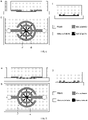
- the inlet microchannels 42 are arranged in parallel, the outlet microchannels 46 are arranged in parallel, and the inlet microchannels 42 and the outlet microchannels 46 form a parallel interdigitated structure. Understandably, referring to FIG. 4 , the inlet microchannels 42 may be arranged at an angle of 0° ⁇ 90°, and the outlet microchannels 46 may be arranged at an angle of 0° ⁇ 90°, and the inlet microchannels 42 and the outlet microchannels 46 may form an oblique interdigitated layout.
- the nanochannels 32 connect the inlet microchannels 42 and the outlet microchannels 46.
- the inlet microchannels 42 and the outlet microchannels 46 may also have other shapes.
- the inlet microchannels 42 have a circular shape
- the outlet microchannels 46 have an annular shape
- the inlet microchannels 42 and the outlet microchannels 46 form a circular interdigitated layout.
- the inlet microchannels 42 have an annular shape
- the outlet microchannels 46 have a circular shape
- the inlet microchannels 42 and the outlet microchannels 46 form a circular interdigitated layout.
- the inlet microchannels 42 have a spiral shape
- the outlet microchannels 46 have a spiral shape
- the inlet microchannels 42 and the outlet microchannels 46 form a spiral interdigitated layout.
- the inlet microchannels 42 have a depth of 1 ⁇ m to 1000 ⁇ m
- the outlet microchannels 46 have a depth of 1 ⁇ m to 1000 ⁇ m.
- the nanochannels 32 have a rectangular parallelepiped shape
- the nanochannels 32 have a depth of 10 nm to 5000 nm, and a width of 10 nm to 1000 ⁇ m.
- the nanochannels 32 have a cylindrical shape
- the nanochannels 32 have a diameter of 10 nm to 5000 nm.
- the width, depth, length, and spacing of the nanochannels 32 may be designed to be of different sizes, as long as the micro- and nano-fluidic chip is operative to process biological particles with different sizes.
- exosomes with a size of 30 nm ⁇ 200 nm microvesicles with a size of 200 nm ⁇ 2000 nm, apoptotic bodies with a size of 500 ⁇ 2000 nm, subcellular particles with a size of 30 nm ⁇ 2000 nm, cell membrane nanoparticles with a diameter of 30 nm ⁇ 2000 nm, artificially synthesized nanoparticles with a size of 30 nm ⁇ 2000 nm that are wrapped in a phospholipid bilayer, or liposomes with a diameter of 30 nm ⁇ 2000 nm, etc.
- inlet microchannels 42, outlet microchannels 46, and nanochannels 32 will not be limited, and different channel numbers may be set according to the throughput requirements of the micro- and nano-fluidic chip.
- the length, width, depth, and spacing of the inlet microchannels 42 and the outlet microchannels 46 will not be limited to a specific size, they are possible as long as a certain volume of mixed solution with the biological particles is able to be injected into the nanochannels 32.
- the inlet of the micro- and nano-fluidic chip will not be limited to one, and multiple inlets may be designed which respectively lead to a biological particle solution such as EVs, a drug cargo solution, a drug-model cargo solution, or a biomolecular cargo solution.
- a biological particle solution such as EVs, a drug cargo solution, a drug-model cargo solution, or a biomolecular cargo solution.
- outlet of the micro- and nano-fluidic chip will not be limited to one, and multiple outlets can be designed which may be used to separately collect cargo-carrying biological particles.
- FIG. 8 there is provided a method for fabricating the above-mentioned micro- and nano-fluidic chip, the fabrication method including the following operations S10, S20, and S30.
- the method includes fabricating a plurality of nanochannels in the first substrate to obtain the nanochannel array layer.
- the plurality of nanochannels may be formed in the first substrate by the etching, nanoimprinting or soft photolithography based on PDMS replica molding, etc.
- the material of the first substrate will not be limited to glass, and it may also be PDMS, quartz, silicon wafer, PMMA, parylene-C, or other commonly used micro- and nano-processing materials.
- the nanochannel array may be fabricated on the top of glass or other materials by using the etching method, or the nanochannel array may be fabricated on the top of the material such as PDMS by the soft photolithography method based on PDMS replica molding, or the nanochannel array may be fabricated on top of material such as PMMA using the nanoimprinting method.
- the method includes fabricating an input unit and/or an output unit on the second substrate, where the input unit includes an inlet microchannel array and at least one inlet, and the output unit includes an outlet microchannel array and at least one outlet, thereby obtaining a microchannel array layer.
- the inlet microchannel array includes at least one inlet microchannel
- the outlet microchannel array includes at least one outlet microchannel
- the inlet microchannels and the outlet microchannels are alternately arranged at intervals.
- the at least one inlet is connected to the inlet microchannel array, and the at least one outlet is connected to the outlet microchannel array.
- the material of the second substrate will not be limited to PDMS, and it may also be glass, quartz, silicon wafer, PMMA, parylene-C, or other commonly used micro- and nano-processing materials.
- the inlet microchannel array and/or the outlet microchannel array may be fabricated on the second substrate by etching, nanoimprinting, or soft photolithography based on PDMS replica molding. That is, the inlet microchannel array and the outlet microchannel array are fabricated on the second substrate. Alternatively, only the inlet microchannel array is fabricated on the second substrate, and the outlet microchannel array is not fabricated. Alternatively, only the outlet microchannel array is fabricated on the second substrate, and the inlet microchannel array is not fabricated. Now referring to FIG. 8 , in the case where only the inlet microchannel array or the outlet microchannel array is fabricated on the second substrate, the corresponding outlet microchannel array or inlet microchannel array needs to be fabricated on a third substrate.
- the soft photolithography method based on PDMS replica molding may be used to fabricate the microchannel array on the bottom of material such as PDMS, or the etching method may be used to etch the microchannel array on the bottom of material such as glass, or a nanoimprint method may be used to fabricated a microchannel array on the bottom of material such as PMMA.
- the method includes alternately stacking and bonding the least one nanochannel array layer and at least one microchannel array layer to obtain the micro- and nano-fluidic chip, wherein each pair of inlet microchannel and outlet microchannel are connected through the plurality of nanochannels.
- the at least one nanochannel array layer and the at least one microchannel array layer are alternately stacked and bonded by oxygen plasma bonding, anodic bonding, fusion bonding, or low-temperature bonding, etc.
- the operation of fabricating a plurality of nanochannels in the first substrate to obtain a nanochannel array layer is as follows.
- a positive photoresist layer is coated on the surface of the first substrate.
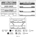
- an exposure treatment is performed using a nanochannel mask as illustrated by e in FIG. 12 .
- the exposed first substrate is immersed in a developer solution for development, and the patterned photoresist film on the developed first substrate is hard baked to obtain the first substrate with a photoresist mask of the nanochannel array, as illustrated by f in FIG. 12 .
- the first substrate may be a glass substrate.
- the first substrate before the positive photoresist layer is coated on the surface of the first substrate, the first substrate may be cleaned and dried, and then the surface of the first substrate may be hydrophilized.
- a spin coating method may be used to coat the surface of the first substrate to form the positive photoresist layer.
- the purpose of the soft baking is to remove the solvent in the positive photoresist layer and improve the adhesion of the photoresist to the first substrate.
- the hard-baking operation includes baking the photoresist mask at a temperature of 90 °C to 130 °C for 5 minutes to 120 minutes to harden the photoresist and improve the adhesion of the photoresist to the first substrate.
- the first substrate with the photoresist mask is etched to obtain a plurality of nanochannels on the surface of the first substrate thus forming the etched first substrate, as illustrated by g in FIG. 12 .
- the etched first substrate is then immersed in an organic solvent or a photoresist remover to remove the photoresist mask on the surface of the etched first substrate thus obtaining the nanochannel array layer, as illustrated by h in FIG. 12 .
- a drying operation may be performed.
- the operation of fabricating a plurality of nanochannels in the first substrate to obtain a nanochannel array layer may be as follows.
- a negative photoresist layer is coated on the surface of a template substrate.
- an exposure treatment is performed using a nanochannel mask.
- the exposed template substrate is subjected to a post-baking treatment.
- the post-baked template substrate is immersed in a developing solution for development, and the patterned photoresist film on the developed template substrate is hard baked to obtain the template substrate with a photoresist mold of the nanochannel array.
- a PDMS mixed solution is cast over the template substrate with the photoresist mold of the nanochannel array.
- the PDMS replica is peeled off from the template substrate to obtain the first substrate with the nanochannel array, that is, the nanochannel array layer.
- the input unit and the output unit are formed on the second substrate, where the input unit includes an inlet microchannel array and at least one inlet, and the output unit includes an outlet microchannel array and at least one outlet, and the operation of fabricating the microchannel array layer is as follows.
- a negative photoresist layer is coated on the surface of the template substrate.
- an exposure treatment is performed using a microchannel mask as illustrated by a in FIG. 12 .
- the exposed template substrate is subjected to a post-baking treatment.
- the post-baked template substrate is immersed in a developer solution for development, and the patterned photoresist film on the developed template substrate is hard baked to obtain the template substrate with a photoresist mold of the microchannel array, as illustrated by b in FIG. 12 .
- the template substrate may be a silicon wafer substrate.
- the template substrate before the negative photoresist layer is coated on the surface of the template substrate, the template substrate is first cleaned and dried, and then the surface of the template substrate is hydrophilized.
- the photoresist is applied by spin coating method.
- a post-baking process is further included.
- the purpose of the soft baking is to remove the solvent in the negative photoresist layer and improve the adhesion of the photoresist to the template substrate.
- post baking is to increase the strength of the negative photoresist in the exposed portions so as to improve the photolithography accuracy.
- the hard-baking operation includes baking the photoresist mold at a temperature of 150 °C to 250 °C for 5 minutes to 120 minutes to harden the photoresist and improve the adhesion of the photoresist to the template substrate.
- a PDMS mixed solution is cast over the template substrate with the photoresist mold of the microchannel array to obtain the second substrate with the inlet microchannel array and the outlet microchannel array, as illustrated by c in FIG. 12 .
- the PDMS mixed solution may be prepared by the following method: the PDMS curing agent and the PDMS prepolymer are mixed in a mass ratio of 1/3 to 1/12 and stirred uniformly to obtain the PDMS mixed solution.
- the photoresist mold of the microchannel array may be pretreated with a release agent. After casting the PDMS mixed solution over the photoresist mold, the PDMS mixed solution may be further baked at a certain temperature to make it cure.
- the PDMS replica is peeled off from the template substrate with the photoresist mold of the microchannel array. Then the PDMS replica with the inlet microchannel array and the outlet microchannel array is punched to fabricate the at least one inlet and the at least one outlet to obtain the microchannel array layer, as illustrated by d in FIG. 12 .
- a hole puncher is used to punch the holes.
- the input unit and the output unit are fabricated on the second substrate, where the input unit includes an inlet microchannel array and at least one inlet, and the output unit includes an outlet microchannel array and at least one outlet, and the operation of fabricating the microchannel array layer may be as follows.
- a positive photoresist layer is coated on the surface of the second substrate. After soft baking, an exposure treatment is performed using a microchannel mask. Then the exposed second substrate is immersed in a developer solution for development, and the patterned photoresist film on the developed second substrate is hard baked to obtain the second substrate with a photoresist mask of the microchannel array.
- the second substrate with the photoresist mask is etched to fabricate a plurality of microchannels on the surface of the second substrate thus forming the etched second substrate.
- the second substrate with the inlet microchannel array and/or the outlet microchannel array is laser-punched to obtain the at least one inlet and the at least one outlet.
- the punched second substrate is immersed in an organic solvent or a photoresist remover, so that the photoresist mask on the surface of the etched second substrate is removed to obtain the microchannel array layer.
- the operation of alternately stacking and bonding the at least one nanochannel array layer and the at least one microchannel array layer includes subjecting the top surface of the first substrate and the bottom surface of the second substrate to oxygen plasma treatment, and then aligning and bonding the top surface of the first substrate with the bottom surface of the second substrate, as illustrated by i in FIG. 12 .
- the method for fabricating the micro- and nano-fluidic chip further includes the following operations: connecting catheters to the inlet and the outlet of the second substrate; see j in FIG. 12 , where the inlet catheter is used for sample input, and the outlet catheter is used for sample output.
- micro- and nano-fluidic chip can be used for on-chip experiments of preparing cargo-carrying biological particles such as EVs. Therefore, the method of use and operation steps of the micro- and nano-fluidic chip on the cargo loading of EVs will be described in further detail below.
- On-chip experiments mainly include isolation of EVs, cargo mixing, chip treatment, cargo diffusion, and sample collection.
- FIGS. 14 and 15 there is provided a method for preparing cargo-carrying biological particles, the method including the following operations.
- the method includes injecting a mixed solution of a biological particle solution of and a cargo solution into the inlet of the above-described micro- and nano-fluidic chip, where the biological particles comprise at least one of EVs, membrane vesicles secreted by the microorganisms, subcellular particles with a size of 30 nm to 2000 nm and having a membrane structure, cell membrane nanoparticles with a size of 30 nm to 2000 nm, artificially synthesized nanoparticles with a size of 30 nm to 2000 nm wrapped in a phospholipid bilayer, and liposomes with a diameter of 30 nm to 2000 nm, etc. ;
- the preparation of the biological particle solution includes the following operations:
- the preparation includes isolating EVs from a biological sample.
- isolating EVs In the operation of isolating EVs from a biological sample, one or a combination of several of the following commonly used methods for isolating EVs may be used: an ultracentrifugal isolation method, a density gradient centrifugal isolation method, a filtration isolation method, an immunocapture isolation method, a precipitation kit isolation method, and so on.
- the biological sample is cell culture supernatant, plasma, serum, urine, saliva, milk, grape, or grapefruit, etc.
- the preparation includes resuspending the EVs in a PBS or cell culture medium, etc. to obtain the biological particle solution.
- the exogenous cargos selected for biological particle loading will not be limited to a specific cargo.
- the cargo may be at least one of the drug cargos, drug-model cargos, or biomolecule cargos, etc. with a size of 500 nm or less.
- the drug cargos with a size less than or equal to 500 nm may be anticancer drugs, drugs for infectious diseases, drugs for cardiovascular diseases, drugs for neurodegenerative diseases, etc.
- the drug-model cargos with a size less than or equal to 500 nm may be protein cargos, nanomaterial cargos, or nucleic acid cargos, etc.
- the biomolecule with a size less than or equal to 500 nm may be probe biomolecules, etc.
- anticancer drugs comprise doxorubicin, curcumin, and paclitaxel, etc.
- the drugs for infectious diseases comprise amphotericin B, ciprofloxacin, rifampicin, and tobramycin, etc.
- the drugs for cardiovascular diseases comprise amiodarone, atenolol, and isosorbide-5-mononitrate, etc.
- the drugs for neurodegenerative diseases comprise dopamine, tanshinone IIA, and levodopa, etc.
- the protein cargos comprise immunoglobulin, interleukin, bovine serum albumin, and endonuclease, etc.
- the nanomaterial cargos comprise quantum dots, carbon nanotubes, and nanoparticles, etc.
- the nucleic acid cargos comprise plasmids, ribonucleic acids, and oligonucleotides, etc.
- the biomolecule cargos comprise potassium ion probe molecules, calcium ion probe molecules, and inositol triphosphate, etc.
- the concentration of the biological particle solution and the concentration of the cargo solution may be set according to actual requirements.
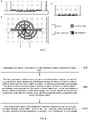
- the mixed solution is injected into the inlet microchannel of the micro- and nano-fluidic chip through an inlet catheter. Due to the obstruction effect of the EV membrane, the cargo molecules can only be distributed outside the EVs, as illustrated by a in FIG. 15 .
- the mixed solution enters the nanochannel through the inlet micro channel. Since the depth of the nanochannel is less than or equal to the diameter of the biological particles, the membrane of the biological particles is mechanically squeezed in the nanochannel so as to introduce pores, and the cargo molecules are convectively transported into the interior of the biological particles from the outside through the pores thus realizing the cargo-loading function.
- the biological particles are EVs
- the EVs and the cargo molecules are squeezed by the nanochannels and then arrive at the outlet microchannel, where the depth of the nanochannels is less than or equal to the diameter of the EVs.
- the transient pores are introduced in the membrane of the EVs under the mechanical compression of the nanochannel thus providing a pass way for cargo transportation, see b in FIG. 15 .
- the EVs enter the smaller nanochannels, the EVs are deformed under the mechanical compression. During this process, the mechanical compression will provide energy to the membrane of the EVs, resulting in reconstitution of the phospholipid bilayer, thereby introducing pores during the reconstitution process.
- the cargo molecules are convectively transported from the outside of the EVs into the inside through these pores under the mechanical effects. Then the EV membrane gradually restores to its intact form, thereby realizing the cargo-loading function, as illustrated by c in FIG. 15 .
- the calcium ion concentration inside and outside the EVs will change, thereby driving the EVs to repair their membranes.
- the chip-treated mixed solution is collected from the outlet, and the cargo-carrying biological particles are obtained by purification process.
- the purification method may comprise ultracentrifugation, density gradient centrifugation, filtration, immunocapture, and precipitation kit method, etc.
- the biological particles will not be limited to being mixed with a special cargo, and may also be mixed with multiple cargos at the same time, so that the multiple cargos can be loaded into the biological particles simultaneously.
- the biological particles are EVs
- the size of the EVs is about 30 nm ⁇ 2000 nm.
- the EVs involved in cargo loading however will not be limited to a specific size, and the EVs that come in multiple sizes may be squeezed for cargo loading in the same micro- and nano-fluidic chip.
- the cargo-carrying biological particles After the cargo-carrying biological particles are prepared, their structure and function are also characterized. In particular, after the cargo-carrying biological particles are obtained, the cargo-loading efficiency, the morphology, and the electrokinetic potential of these biological particles can be characterized using one or more selected from the following analytical methods, including flow cytometry, super-resolution optical imaging system, scanning electron microscope, transmission electron microscope, atomic force microscope, cryo-electron microscope, nanoparticle tracking analysis, and so on. In addition, functional characterization of the cargo-carrying biological particles may also be performed, for example, co-incubating the cargo-carrying biological particles with different types of cells or tissues in vitro, and observing the process of the biological particles delivering cargos into these cells or tissues in vitro. Additionally or alternatively, the cargo-carrying biological particles may also be used to carry out animal experiments to explore the treatment process and therapeutic effect of biological particles carrying cargos to the lesion or focal tissue in the animal body.
- analytical methods including flow cytometry, super-
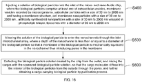
- a solution of biological particles is injected into the inlet of the above-described micro- and nano-fluidic chip, where the biological particles include at least one of EVs, membrane vesicles secreted by the microorganisms, subcellular particles with a size of 30 nm to 2000 nm and having a membrane structure, cell membrane nanoparticles with a size of 30 nm to 2000 nm, artificially synthesized nanoparticles with a size of 30 nm to 2000 nm wrapped in a phospholipid bilayer, or liposomes with a diameter of 30 nm to 2000 nm, etc.
- the biological particles include at least one of EVs, membrane vesicles secreted by the microorganisms, subcellular particles with a size of 30 nm to 2000 nm and having a membrane structure, cell membrane nanoparticles with a size of 30 nm to 2000 nm, artificially synthesized nanoparticles with a size of 30 nm to
- the solution of biological particles enters the nanochannels through the inlet microchannels. Since the depth of the nanochannel is less than or equal to the diameter of the biological particles, the membrane of the biological particles is mechanically squeezed in the nanochannel so as to introduce pores.
- the solution of the biological particles having been squeezed is collected from the outlet, and mixing the exogenous cargos with the squeezed biological particle solution, so that the cargo molecules diffuse into the interior of the biological particles from the outside through the pores, and further obtaining the cargo-carrying biological particles by purification process.
- micro- and nano-fluidic chip can not only be used for squeezing biological particles for cargo loading, but also for applications in synthesizing liposomes and squeezing the liposomes for cargo loading, synthesizing cell membrane fragments into cell membrane nanoparticles and squeezing them for cargo loading, or the application in cargo loading of artificially synthesized nanoparticles that are wrapped by a phospholipid bilayer.
- the above-described micro- and nano-fluidic chip has a unique layout.
- the design of the micro- and nano-fluidic chip is scalable, that is, the number and shape of the microchannel array and nanochannel array can be designed according to experimental requirements.
- the method of fabricating the micro- and nano-fluidic chip is simple and diverse and easy to implement.
- the layout parameters of the nanochannel array have the characteristics of high throughput and flexible design.
- the depth, width, length, spacing, and number can be designed or changed according to requirements of cargo-loading throughput, sizes of exogenous cargos, or requirements of cargo-loading efficiency.
- the cargo loading of biological particles such as EVs is versatile for all types and sizes of exogenous cargos.
- one or more drug cargos, drug-model cargos, or biomolecule cargos may be loaded at the same time into different types or sizes of EVs (30 nm ⁇ 2000 nm in size), subcellular particles having membrane structures (30 nm ⁇ 2000 nm in size), cell membrane nanoparticles (30 nm ⁇ 2000 nm in size), artificially synthesized nanoparticles (30 nm ⁇ 2000 nm in size) wrapped by a phosphate bilayer, liposomes (30 nm ⁇ 2000 nm in size), or membrane vesicles (30 nm ⁇ 2000 nm in size) secreted by bacteria and other microorganisms.
- Biological particles such as EVs are versatile for all types of drugs, drug models or biomolecule cargos, as long as it is satisfied that the size is less than or equal to 500 nm.
Landscapes
- Health & Medical Sciences (AREA)
- Chemical & Material Sciences (AREA)
- Physics & Mathematics (AREA)
- General Physics & Mathematics (AREA)
- General Health & Medical Sciences (AREA)
- Chemical Kinetics & Catalysis (AREA)
- Analytical Chemistry (AREA)
- Dispersion Chemistry (AREA)
- Hematology (AREA)
- Clinical Laboratory Science (AREA)
- Spectroscopy & Molecular Physics (AREA)
- Life Sciences & Earth Sciences (AREA)
- Pharmacology & Pharmacy (AREA)
- Epidemiology (AREA)
- Medicinal Chemistry (AREA)
- Animal Behavior & Ethology (AREA)
- Public Health (AREA)
- Veterinary Medicine (AREA)
- Molecular Biology (AREA)
- Fluid Mechanics (AREA)
- Dermatology (AREA)
- Physical Or Chemical Processes And Apparatus (AREA)
Abstract
Description
- This invention relates to the field of microelectromechanical system technology, microfluidic technology and nanofluidic technology, and more particularly relates to a micro- and nano-fluidic chip, a method of fabricating the same, and applications thereof.
- With the rise of nanotechnology, a variety of nano-delivery systems (NDSs) have been proposed in succession, aiming to carry small molecules, nucleic acids, proteins, or other exogenous cargos into the body or focal lesion, which is not only helpful for the diagnosis and treatment of cancers, infectious diseases, cardiovascular diseases, and neurodegenerative diseases, etc., but are also conducive to improving the therapeutic effect and reducing negative effects such as organ toxicity. Thus, the construction of new types of NDSs has major theoretical significance and practical value for experimental research and clinical application.
- For the time being, commonly used NDSs include nanoparticles, liposomes, and viral vectors, etc. These NDSs, however, face a variety of problems in clinical applications, such as organ toxicity, immune clearance, insertional mutagenesis, and short circulation duration within the body. Biological particles such as extracellular vesicles (EVs) having a diameter of about 30 nm ~ 2000 nm, which originate from the secretion of cells, the secretion of microorganisms, or may be derived from artificial synthesis, are regarded as a natural communication medium or delivery vehicle. They can not only realize the transfer and transportation of substances, but also have the advantages of low immunogenicity, biodegradability, non-toxicity, high carrying capacity, and strong tissue penetration. Therefore, they have been regarded as a new type of NDS in recent years.
- In order to deliver exogenous cargos into the interior of biological particles such as EVs, commonly used methods include incubation and electroporation. The incubation method includes mixing the cargos with the biological particles uniformly under a certain temperature, and so the cargo molecules gradually diffuse into the interior of the biological particles along the concentration gradient thereby achieving cargo loading. Although the incubation method is simple and easy to operate, this method generally has a problem of low cargo-loading efficiency. Electroporation, as another commonly used cargo-loading method, includes stimulating the biological particles by applying an electric field so that some temporary pores would appear on the membrane surface. As such, the cargo molecules are convectively transported into the biological particles through the pores. Then after a certain period of time, the membrane of biological particles returns to their original intact state. In this way, the cargos are packaged in the biological particles, thus accomplishing the cargo-loading process. While this method improves the cargo-loading efficiency, the external electric field may induce excessive damages on both biological particles such as EVs and their carrying cargos.
- Micro-/Nano-fluidics is a technology for studying and applying the properties of fluids and their contents at the micro- or nano-scale. Microfluidic chips have been used in cellular loading, but there are no micro- and nano-fluidic chips applied to the study of cargo loading of biological particles such as EVs.
- In view of this, there is a need to provide a micro- and nano-fluidic chip that can be used for cargo loading of biological particles such as EVs, a method of fabricating the micro- and nano-fluidic chip, and a method of preparing cargo-carrying biological particles.
- There is provided a micro- and nano-fluidic chip, comprising at least one nanochannel array layer and at least one microchannel array layer, where the at least one nanochannel array layer and the at least one microchannel array layer are alternately stacked.
- The at least one nanochannel array layer includes at least one nanochannel.
- The at least one microchannel array layer includes an input unit and/or an output unit. The input unit includes an inlet microchannel array and at least one inlet, and the output unit includes an outlet microchannel array and at least one outlet. The inlet microchannel array includes at least one inlet microchannel, and the outlet microchannel array includes at least one outlet microchannel, where the at least one inlet microchannel and the at least one outlet microchannel are alternately arranged at intervals. The at least one inlet is connected to the at least one inlet microchannel, and the at least one outlet is connected to the at least one outlet microchannel. Each pair of inlet microchannel and outlet microchannel are bridged by the at least one nanochannel.
- In the case where the at least one microchannel array layer is one layer, the microchannel array layer includes the input unit and the output unit. When the nanochannel array connects the at least one inlet microchannel array and the at least one outlet microchannel array, the extension direction of the at least one nanochannel is set perpendicularly to or at an angle of 0° ~ 90° with the microchannel array layer.
- In the case where the microchannel array includes two or more layers, one of the microchannel array layers includes the input unit, and another of the microchannel array layers includes the output unit, and the nanochannel array layer is arranged between every two adjacent microchannel array layers. When the nanochannel array connects the inlet microchannel array and the outlet microchannel array, the extension direction of the at least one nanochannel is set perpendicularly to or at an angle of 0° ~ 90° with the microchannel array layers.
- In one embodiment, the at least one nanochannel array layer is made of polydimethylsiloxane (PDMS), glass, quartz, silicon wafer, poly (methyl methacrylate) (PMMA), or parylene-C, etc., and the at least one microchannel array layer is made of PDMS, glass, quartz, silicon wafer, PMMA, or parylene-C, etc.
- In one embodiment, in the case where the at least one nanochannel array includes at least two nanochannels, the nanochannels of the nanochannel array layer are arranged in parallel with or at an angle of 0° to 90° with respect to one another.
- In one embodiment, in the case where there are one inlet microchannel and one outlet microchannel, the inlet microchannel and the outlet microchannel are arranged in parallel with each other; or
- in the case where there are provided two or more inlet microchannels and two or more outlet microchannels, the inlet microchannels are arranged in parallel, the outlet microchannels are arranged in parallel, and the inlet microchannels are arranged in parallel with the outlet microchannels forming a parallel interdigitated layout; or
- in the case where there are provided two or more inlet microchannels and two or more outlet microchannels, the inlet microchannels are arranged at an angle of 0° to 90° with respect to each other, the outlet microchannels are arranged at an angle greater than 0° and less than or equal to 90° with respect to each other, and the inlet microchannels and the outlet microchannels are arranged to form an oblique interdigitated layout; or
- the at least one inlet microchannel has a circular shape, the at least one outlet microchannel has an annular shape, and the at least one inlet microchannel and the at least one outlet microchannel form a circular interdigitated layout; or
- the at least one inlet microchannel has an annular shape, the at least one outlet microchannel has a circular shape, and the at least one inlet microchannel and the at least one outlet microchannel form a circular interdigitated layout; or
- the at least one inlet microchannel has a spiral shape, the at least one outlet microchannel has a spiral shape, and the at least one inlet microchannel and the at least one outlet microchannel form a spiral interdigitated layout.
- In one embodiment, the at least one inlet microchannel has a depth of 1 µm to 1000 µm, and the at least one outlet microchannel has a depth of 1 µm to 1000 µm;
- in the case where the at least one nanochannel has a rectangular parallelepiped shape, the at least one nanochannel has a depth dimension of 10 nm to 5000 nm, and a width dimension of 10 nm to 1000 µm; or
- in the case where the at least one nanochannel has a cylindrical shape, the at least one nanochannel has a diameter of 10 nm to 5000 nm.
- There is also provided a method of fabricating a micro- and nano-fluidic chip, including:
- fabricating a plurality of nanochannels in the first substrate to obtain a nanochannel array layer;
- creating an input unit and/or an output unit in the second substrate, where the input unit includes an inlet microchannel array and at least one inlet, and the output unit includes an outlet microchannel array and at least one outlet, thereby obtaining a microchannel array layer; the inlet microchannel array includes at least one inlet microchannel, and the outlet microchannel array includes at least one outlet microchannel; the at least one inlet microchannel and the at least one outlet microchannel are alternately arranged at intervals; and the inlet is connected to the at least one inlet microchannel, and the outlet is connected to the at least one outlet microchannel.
- alternately stacking and bonding the at least one nanochannel array layer and at least one microchannel array layer to obtain the micro- and nano-fluidic chip, wherein the at least one inlet microchannel and the at least one outlet microchannel are connected through the plurality of nanochannels.
- In one embodiment, the plurality of nanochannels are fabricated in the first substrate by etching, nanoimprinting, or soft photolithography based on PDMS replica molding, etc.
- In one embodiment, the operation process of fabricating the plurality of nanochannels in the first substrate to obtain the nanochannel array layer is as follows.
- A positive photoresist layer is coated on the surface of the first substrate. After soft baking, an exposure treatment is performed using a nanochannel mask. Then the exposed first substrate is immersed in a developer solution for development. After hard baking of the patterned photoresist film, the first substrate with a photoresist mask of the nanochannel array is obtained.
- Then the first substrate with the photoresist mask is etched to obtain a plurality of nanochannels on the surface of the first substrate thus forming the etched first substrate.
- The etched first substrate is then immersed in an organic solvent or a photoresist remover to remove the photoresist mask on the surface of the etched first substrate thus obtaining the nanochannel array layer.
- In one embodiment, the operation process of fabricating the plurality of nanochannels in the first substrate to obtain the nanochannel array layer is as follows.
- A negative photoresist layer is coated on the surface of a template substrate. After soft baking, an exposure treatment is performed using a nanochannel mask. Then the exposed template substrate is subjected to a post-baking treatment. Next, the post-baked template substrate is immersed in a developer for development. After hard baking of the patterned photoresist film, the template substrate with a photoresist mold of the nanochannel array is obtained.
- Then a PDMS mixed solution is cast over the template substrate with the photoresist mold of the nanochannel array. After a curing process, the PDMS replica is peeled off from the template substrate to obtain the first substrate with the nanochannel array, that is, the nanochannel array layer.
- In one embodiment, the inlet microchannel array and/or the outlet microchannel array are created in the second substrate by etching, nanoimprinting, or soft photolithography based on PDMS replica molding, etc.
- In one embodiment, the input unit and the output unit are fabricated on the second substrate, where the input unit includes an inlet microchannel array and at least one inlet, and the output unit includes an outlet microchannel array and at least one outlet, and the operation process of obtaining the microchannel array layer is as follows.
- A negative photoresist layer is coated on the surface of a template substrate. After soft baking, an exposure treatment is performed using a microchannel mask. Then the exposed template substrate is subjected to a post-baking treatment. Next, the post-baked template substrate is immersed in a developing solution for development. After hard baking of the patterned photoresist film, the template substrate with a photoresist mold of the microchannel array is obtained.
- Then the PDMS mixed solution is poured on the template substrate with the photoresist mold of the microchannel array. After a curing process, the PDMS replica is peeled off from the photoresist mold to obtain the second substrate with the inlet microchannel array and/or the outlet microchannel array.
- Then the second substrate with the inlet microchannel array and/or the outlet microchannel array is punched to make the at least one inlet and the at least one outlet thus obtaining the microchannel array layer.
- In one embodiment, the input unit and the output unit are fabricated on the second substrate, where the input unit includes an inlet microchannel array and at least one inlet, and the output unit includes an outlet microchannel array and at least one outlet, and the operation process of obtaining the microchannel array layer is as follows.
- A positive photoresist layer is coated on the surface of the second substrate. After soft baking, an exposure treatment is performed using a microchannel mask. Then the exposed second substrate is immersed in a developer solution for development. After hard baking of the patterned photoresist film, the second substrate with a photoresist mask of the microchannel array is obtained.
- Then the second substrate with the photoresist mask is etched to fabricate a plurality of microchannels on the surface of the second substrate thus forming the etched second substrate.
- After the etching, the second substrate with the inlet microchannel array and/or the outlet microchannel array is laser-punched to make the at least one inlet and the at least one outlet.
- The punched second substrate is immersed in an organic solvent or a photoresist remover, so that the photoresist mask on the surface of the etched second substrate is removed to obtain the microchannel array layer.
- In one embodiment, the at least one nanochannel array layer and the at least one microchannel array layer are alternately stacked and bonded by oxygen plasma bonding, anodic bonding, fusion bonding, or low-temperature bonding, etc.
- In one embodiment, the operation process of alternately stacking and bonding the at least one nanochannel array layer and the at least one microchannel array layer includes subjecting the top surface of the first substrate and the bottom surface of the second substrate to oxygen plasma treatment, and then aligning and bonding the top surface of the first substrate with the bottom surface of the second substrate.
- There is further provided a method of preparing cargo-carrying biological particles, the method including the following operations:
- injecting a mixed solution of a biological particle solution and a cargo solution into the at least one inlet of the micro- and nano-fluidic chip as recited in claim 1, where the biological particles comprise at least one of EVs, membrane vesicles secreted by the microorganisms, subcellular particles with a size of 30 nm to 2000 nm and having a membrane structure, cell membrane nanoparticles with a size of 30 nm to 2000 nm, artificially synthesized nanoparticles with a size of 30 nm to 2000 nm wrapped in a phospholipid bilayer, or liposomes with a diameter of 30 nm to 2000 nm, etc.
- where the mixed solution enters the at least one nanochannel through the at least one inlet microchannel, and because the depth, width, or diameter of the at least one nanochannel is less than or equal to the diameter of the biological particles, the membrane of the biological particles is mechanically squeezed in the at least one nanochannel so as to introduce pores, and the cargo molecules are convectively transported into the interior of the biological particles from the outside through the pores thus realizing the cargo-loading function; and
- collecting the chip-treated mixed solution from the at least one outlet of the micro- and nano-fluidic chip, and obtaining the cargo-carrying biological particles by a purification process.
- In one embodiment, in the case where the biological particles are EVs, the preparation of the biological particle solution includes the following operations:
- isolating EVs from a biological sample; and then
- resuspending the EVs in a phosphate-buffered saline (PBS) or cell culture medium to obtain the biological particle solution, etc.
- In one embodiment, in the operation of isolating the EVs from a biological sample, an ultracentrifugal isolation method, a density gradient centrifugal isolation method, a filtration isolation method, an immunocapture isolation method, or a precipitation kit isolation method, etc. is used.
- In one embodiment, the biological sample is cell culture supernatant, plasma, serum, urine, saliva, milk, grape, or grapefruit, etc.
- In one embodiment, the exogenous cargos in the cargo solution comprise at least one of drug cargos with a size of 500 nm or less, drug-model cargos with a size of 500 nm or less, and biomolecule cargos with a size of 500 nm or less, etc.
- In one embodiment, the drug cargos with a size less than or equal to 500 nm comprise anticancer drugs, drugs for infectious diseases, drugs for cardiovascular diseases, and drugs for neurodegenerative diseases, etc. The drug-model cargos with a size less than or equal to 500 nm comprise protein cargos, nanomaterial cargos, and nucleic acid cargos, etc. The biomolecule cargos with a size less than or equal to 500 nanometers comprise probe biomolecules, etc.
- In one embodiment, the anticancer drugs comprise doxorubicin, curcumin, and paclitaxel, etc.
- the drugs for infectious diseases comprise amphotericin B, ciprofloxacin, rifampicin, and tobramycin, etc.
- the drugs for cardiovascular diseases comprise amiodarone, atenolol, and isosorbide-5-mononitrate, etc.
- the drugs for neurodegenerative diseases comprise dopamine, tanshinone IIA and levodopa, etc.
- the protein cargos comprise immunoglobulin, interleukin, bovine serum albumin, and endonuclease, etc.
- the nanomaterial cargos comprise quantum dots, carbon nanotubes, and nanoparticles, etc.
- the nucleic acid cargos comprise plasmids, ribonucleic acids, deoxyribonucleic acids, and oligonucleotides, etc.
- the biomolecule cargos comprise potassium ion probe molecules, calcium ion probe molecules, and inositol triphosphate, etc.
- In one embodiment, the purification methods comprise ultracentrifugation, density gradient centrifugation, filtration, immunocapture, and precipitation kit method, etc.
- There is further provided a method of preparing cargo-carrying biological particles, the method including the following operations:
- injecting the solution of biological particles into the at least one inlet of the above-described micro- and nano-fluidic chip, where the biological particles comprise at least one of the EVs, membrane vesicles secreted by the microorganisms, subcellular structures with a size of 30 nm to 2000 nm and having a membrane structure, cell membrane nanoparticles with a size of 30 nm to 2000 nm, artificially synthesized nanoparticles with a size of 30 nm to 2000 nm wrapped in a phospholipid bilayer, and liposomes with a diameter of 30 nm to 2000 nm, etc.
- where the solution of biological particles enters the at least one nanochannel through the at least one inlet microchannel, and because the depth, width, or diameter of the at least one nanochannel is less than or equal to the diameter of the biological particles, the membrane of the biological particles is mechanically squeezed in the at least one nanochannel so as to introduce pores; and
- collecting the chip-treated solution of the biological particles from the at least one outlet of the micro- and nano-fluidic chip, and mixing the exogenous cargos with the squeezed biological particle solution, so that the cargo molecules diffuse into the interior of the biological particles from the outside through the pores, and further obtaining the cargo-carrying biological particles by the purification process.
- Further disclosed are applications of the above-described micro- and nano-fluidic chip in squeezing biological particles for cargo loading, synthesizing liposomes and squeezing the liposomes for cargo loading, synthesizing cell membrane fragments into cell membrane nanoparticles and squeezing them for cargo loading, or the application in cargo loading of artificially synthesized nanoparticles that are wrapped by a phospholipid bilayer.
- Further disclosed are applications of the above-described micro- and nano-fluidic chip that is fabricated using the above-mentioned method in squeezing biological particles for cargo loading, synthesizing liposomes and squeezing the liposomes for cargo loading, synthesizing cell membrane fragments into cell membrane nanoparticles and squeezing them for cargo loading, or the application in cargo loading of artificially synthesized nanoparticles that are wrapped by a phospholipid bilayer structure.
- In the above-described micro- and nano-fluidic chip, the inlet microchannels and the outlet microchannels are connected to each other through the nanochannels, so that after the sample is injected into the nanochannels from the inlet microchannels, it will be mechanically squeezed by the nanochannels to reach the outlet microchannels. Since the depth, width or diameter of the nanochannels is similar to the size of biological particles, biological particles such as EVs ranging from 30 nm to 2000 nm can be effectively mechanically squeezed, so that the membrane of biological particles such as EVs can be permeabilized allowing for the loading of a variety of drug cargos, drug-model cargos, or biomolecule cargos with different sizes. Compared with the existing electroporation methods, the present invention not only avoids the use of an external electric field, but also avoids the problems of agglomeration and viability reduction of biological particles such as EVs. Because the need for special instruments for applying an electric field is eliminated, the cost is effectively reduced, which is helpful for technology promotion or industrial application. In addition, by providing multiple inlet microchannels, outlet microchannels and nanochannels, it has the advantage of high throughput, which can effectively increase the throughput of the cargo-loading process, and solves the problem of low cargo-loading efficiency in common incubation methods. The above-mentioned micro- and nano-fluidic chip can not only be used for cargo-loading research of biological particles such as EVs, but also has the potential to be promoted in clinical applications, so as to meet the needs of experimental research and clinical applications for NDSs.
- The above-described method of fabricating the micro- and nano-fluidic chip is simple and straightforward to operate.
- The above-mentioned method of preparing cargo-carrying biological particles is simple and straightforward to operate. The nanochannels can effectively mechanically squeeze the biological particles, so that the membrane of biological particles such as EVs can be permeabilized allowing for the loading of a variety of drug cargos, drug-model cargos or biomolecule cargos with different sizes. Compared with the existing electroporation methods, the present invention not only avoids the use of an external electric field, but also avoids the problems of agglomeration and viability reduction of biological particles such as EVs. Because the need for special instruments for applying an electric field is eliminated, the cost is effectively reduced, which is helpful for technology promotion or industrial application.
-
-
FIG. 1a is a front view of a micro- and nano-fluidic chip according to an embodiment of this invention. -
FIG. 1b is a top view of the micro- and nano-fluidic chip shown inFIG. 1a . -
FIG. 1c is a left side view of the micro- and nano-fluidic chip shown inFIG. 1a . -
FIG. 2a is a front view of a micro- and nano-fluidic chip according to another embodiment of this invention. -
FIG. 2b is a top view of the micro- and nano-fluidic chip shown inFIG. 2a . -
FIG. 2c is a left side view of the micro- and nano-fluidic chip shown inFIG. 2a . -
FIG. 3a is a front view of a micro- and nano-fluidic chip according to yet another embodiment of this invention. -
FIG. 3b is a top view of the micro- and nano-fluidic chip shown inFIG. 3a . -
FIG. 3c is a left side view of the micro- and nano-fluidic chip shown inFIG. 3a . -
FIG. 4a is a front view of a micro- and nano-fluidic chip according to still another embodiment of this invention. -
FIG. 4b is a top view of the micro- and nano-fluidic chip shown inFIG. 4a . -
FIG. 4c is a left side view of the micro- and nano-fluidic chip shown inFIG. 4a . -
FIG. 5a is a front view of a micro- and nano-fluidic chip according to still another embodiment of this invention. -
FIG. 5b is a top view of the micro- and nano-fluidic chip shown inFIG. 5a . -
FIG. 5c is a left side view of the micro- and nano-fluidic chip shown inFIG. 5a . -
FIG. 6a is a front view of a micro- and nano-fluidic chip according to still another embodiment of this invention. -
FIG. 6b is a top view of the micro- and nano-fluidic chip shown inFIG. 6a . -
FIG. 6c is a left side view of the micro- and nano-fluidic chip shown inFIG. 6a . -
FIG. 7a is a front view of a micro- and nano-fluidic chip according to still another embodiment of this invention. -
FIG. 7b is a top view of the micro- and nano-fluidic chip shown inFIG. 7a . -
FIG. 7c is a left side view of the micro- and nano-fluidic chip shown inFIG. 7a . -
FIG. 8 is a flowchart of a method of fabricating a micro- and nano-fluidic chip according to an embodiment of this invention. -
FIG. 9 is a flowchart of a method of fabricating a nanochannel array layer according to an embodiment of this invention. -
FIG. 10 is a flowchart of a method of fabricating a nanochannel array layer according to another embodiment of this invention. -
FIG. 11 is a flowchart of a method of fabricating a microchannel array layer according to an embodiment of this invention. -
FIG. 12 is a schematic diagram illustrating a method of fabricating the micro- and nano-fluidic chip. -
FIG. 13 is a flowchart of a method of fabricating the microchannel array layer according to another embodiment of this invention. -
FIG. 14 is a flowchart of a method of preparing cargo-carrying biological particles according to an embodiment of this invention. -
FIG. 15 is a schematic diagram illustrating the reaction mechanism of the method of preparing the cargo-carrying biological particles. -
FIG. 16 is a flowchart of a method of preparing cargo-carrying biological particles according to another embodiment of this invention. - For a better understanding of the objectives, technical solutions, and advantages of the present invention, hereinafter the present invention will be described in further detail in connection with the accompanying drawings and some illustrative embodiments. It is to be understood that the specific embodiments described here are intended for the mere purposes of illustrating this invention, instead of limiting. As used herein, a "fixed connection" includes a direct fixed connection and an indirect fixed connection.
- The biological particles in this application refer to the EVs, membrane vesicles secreted by the microorganisms, subcellular particles having a membrane structure, cell membrane nanoparticles, artificially synthesized nanoparticles wrapped in a phospholipid bilayer, or liposomes that have a size of 30 nm to 2000 nm.
- As illustrated in
FIGS. 1 and 2 , the micro- and nano-fluidic chip according to one embodiment includes at least onenanochannel array layer 30 and at least onemicrochannel array layer 40. Thenanochannel array layer 30 and themicrochannel array layer 40 are alternately stacked. - The
nanochannel array layer 30 includes at least onenanochannel 32. - The
microchannel array layer 40 includes an input unit and an output unit. The input unit includes an inlet microchannel array and at least oneinlet 10, and the output unit includes an outlet microchannel array and at least oneoutlet 20. The inlet microchannel array includes at least oneinlet microchannel 42, and the outlet microchannel array includes at least oneoutlet microchannel 46, where the at least oneinlet microchannel 42 and the at least onemicrochannel 46 are alternately arranged at intervals. The at least oneinlet 10 is connected to the at least oneinlet microchannel 42, and the at least oneoutlet 20 is connected to the at least oneoutlet microchannel 46. Each pair ofinlet microchannel 42 andoutlet microchannel 46 are bridged by the at least onenanochannel 32. - As illustrated in
FIG. 1 , when themicrochannel array layer 40 is one layer, themicrochannel array layer 40 includes an input unit and an output unit. When thenanochannels 32 connects themicrochannels 42 and themicrochannels 46, the extension direction of thenanochannels 32 is set perpendicularly to or at an angle of 0° ~ 90° with themicrochannel array layer 40. - Now referring to
FIG. 2 , when themicrochannel array layer 40 has two or more layers, one of the microchannel array layers 40 includes the input unit, and the othermicrochannel array layer 40 includes the output unit. Thenanochannel array layer 30 is arranged between the two adjacent microchannel array layers 40. When the at least onenanochannel 32 connects the at least oneinlet microchannel 42 to the at least oneoutlet microchannel 46, the extension direction of the at least onenanochannel 32 is set perpendicularly to or at an angle of 0° ~ 90° with themicrochannel array layer 40. - In particular, in the embodiment illustrated in
FIG. 2 , themicrochannel array layer 40 includes two layers. In the above-described micro- and nano-fluidic chip, the inlet microchannels 42 and the outlet microchannels 46 are connected to each other through thenanochannels 32, so that after the sample is injected into thenanochannels 32 from the inlet microchannels 42, it will be mechanically squeezed by thenanochannels 32 to reach the outlet microchannels 46. Since the depth, width or diameter of thenanochannels 32 is similar to the size of biological particles, the biological particles such as EVs can be effectively mechanically squeezed, so that the membrane of biological particles can be permeabilized allowing for the loading of a variety of drug cargos, drug-model cargos or biomolecule cargos with different sizes. Compared with the existing electroporation methods, the present invention not only avoids the use of an external electric field, but also avoids the problems of agglomeration and viability reduction of biological particles such as EVs. Because the need for special instruments for applying an electric field is eliminated, the cost is effectively reduced, which is helpful for technology promotion or industrial application. In addition, by providing multiple inlet microchannels 42, outlet microchannels 46 and nanochannels 32, it has the advantage of high throughput, which can effectively increase the throughput of the cargo-loading process, and solves the problem of low cargo-loading efficiency in common incubation methods. The above-mentioned micro- and nano-fluidic chip can not only be used for cargo-loading research of biological particles such as EVs, but also has the potential to be promoted in clinical applications, so as to meet the needs of experimental research and clinical applications for NDSs. - In the embodiment illustrated in
FIG. 1 , the substrate of thenanochannel array layer 30 is aglass substrate 34. It will be appreciated that the material of thenanochannel array layer 30 will not be limited to glass, and it may also be PDMS, quartz, silicon wafer, PMMA, parylene-C, or other commonly used micro- and nano-processing materials. - In the embodiment illustrated in
FIG. 1 , the material of themicrochannel array layer 40 is PDMS 44. It will be appreciated that the material of themicrochannel array layer 40 will not be limited to PDMS, and it may also be glass, quartz, silicon wafer, PMMA, parylene-C, or other commonly used micro- and nano-processing materials. - The
nanochannel array layer 30 and themicrochannel array layer 40 will not be limited to be separately disposed in the upper and lower substrates; they may also be disposed in the same substrate. - In the embodiment illustrated in
FIG. 1 , each of thenanochannel array layer 30 and themicrochannel array layer 40 has only one layer. It will be appreciated that the micro- and nano-fluidic chip will also not be limited to two layers, and can be expanded into multiple layers, as long as there is arranged ananochannel array layer 30 between any two microchannel array layers 40 for connection. - In the case where the nanochannel array includes at least two nanochannels, the nanochannels of the nanochannel array layer may be arranged in parallel with or at an angle of 0° to 90° with respect to each other. In the embodiment illustrated in
FIG. 1 , thenanochannels 32 of thenanochannel array layer 30 are arranged in parallel. It will be appreciated that the nanochannels 32 don't need to be arranged completely in parallel, as long as thenanochannels 32 are operative to connect the inlet microchannels 42 and the outlet microchannels 46. For example, in the embodiment illustrated inFIG. 7 , the nanochannels intersect each other at an angle of 0° to 90°. - Now referring to
FIG. 3 , in the case where there is provided one of the inlet microchannels 42 and one of the outlet microchannels 46, theinlet microchannel 42 and theoutlet microchannel 46 may be arranged in parallel. InFIG. 3 , there are provided three of thenanochannels 32. It will be appreciated however that it will not be limited to three in practice, but the number ofnanochannels 32 is at least one. - In the case where there are two or more of the inlet microchannels and two or more of the outlet microchannels, as is the case in the embodiment illustrated in
FIG. 1 , theinlet 10 is connected to the inlet microchannels 42 through the inlet connecting channel. In particular, theinlet 10 is connected to the inlet connecting channel. The plurality of inlet microchannels 42 are arranged in parallel and one end of the plurality of inlet microchannels 42 is connected to the inlet connecting channel. Theoutlet 20 is connected to the outlet microchannels 46 through an outlet connecting channel. In particular, theoutlet 20 is connected to the outlet connecting channel. The plurality of outlet microchannels 46 are arranged in parallel and one end of the multiple outlet microchannels 46 is connected to the outlet connecting channel. The inlet microchannels 42 and the outlet microchannels 46 are alternately arranged at intervals. It can be understood that the inlet microchannels 42 and the outlet microchannels 46 don't have to be arranged completely in parallel, as long as the inlet microchannels 42 and the outlet microchannels 46 are spaced apart from each other. - Further, in the embodiment illustrated in
FIGS. 1 and 2 , the extension direction of thenanochannels 32 is perpendicular to the extension direction of the inlet microchannels 42 and the outlet microchannels 46. It will be appreciated that the extension direction of the nanochannels 32 will not be limited to being perpendicular to the extension direction of the inlet microchannels 42 and the outlet microchannels 46, and they may be arranged at an angle of 0° ~ 90°, as long as thenanochannels 32 are operative to connect the inlet microchannels 42 and the outlet microchannels 46. - In the embodiment illustrated in
FIG. 1 , the inlet microchannels 42 are arranged in parallel, the outlet microchannels 46 are arranged in parallel, and the inlet microchannels 42 and the outlet microchannels 46 form a parallel interdigitated structure. Understandably, referring toFIG. 4 , the inlet microchannels 42 may be arranged at an angle of 0° ~ 90°, and the outlet microchannels 46 may be arranged at an angle of 0° ~ 90°, and the inlet microchannels 42 and the outlet microchannels 46 may form an oblique interdigitated layout. The nanochannels 32 connect the inlet microchannels 42 and the outlet microchannels 46. - In other embodiments, the inlet microchannels 42 and the outlet microchannels 46 may also have other shapes. For example, referring to
FIG. 5 , the inlet microchannels 42 have a circular shape, the outlet microchannels 46 have an annular shape, and the inlet microchannels 42 and the outlet microchannels 46 form a circular interdigitated layout. - Now referring to
FIG. 6 , in another embodiment, the inlet microchannels 42 have an annular shape, the outlet microchannels 46 have a circular shape, and the inlet microchannels 42 and the outlet microchannels 46 form a circular interdigitated layout. - Now referring to
FIG. 7 , in another embodiment, the inlet microchannels 42 have a spiral shape, the outlet microchannels 46 have a spiral shape, and the inlet microchannels 42 and the outlet microchannels 46 form a spiral interdigitated layout. - In one embodiment, the inlet microchannels 42 have a depth of 1 µm to 1000 µm, and the outlet microchannels 46 have a depth of 1 µm to 1000 µm. In the case where the
nanochannels 32 have a rectangular parallelepiped shape, thenanochannels 32 have a depth of 10 nm to 5000 nm, and a width of 10 nm to 1000 µm. In the case where thenanochannels 32 have a cylindrical shape, thenanochannels 32 have a diameter of 10 nm to 5000 nm. It will be appreciated that in actual operation, the width, depth, length, and spacing of the nanochannels 32 may be designed to be of different sizes, as long as the micro- and nano-fluidic chip is operative to process biological particles with different sizes. For example, exosomes with a size of 30 nm ~ 200 nm, microvesicles with a size of 200 nm ~ 2000 nm, apoptotic bodies with a size of 500 ~ 2000 nm, subcellular particles with a size of 30 nm ~ 2000 nm, cell membrane nanoparticles with a diameter of 30 nm ~ 2000 nm, artificially synthesized nanoparticles with a size of 30 nm ~ 2000 nm that are wrapped in a phospholipid bilayer, or liposomes with a diameter of 30 nm ~ 2000 nm, etc. - It can be understood that the number of inlet microchannels 42, outlet microchannels 46, and nanochannels 32 will not be limited, and different channel numbers may be set according to the throughput requirements of the micro- and nano-fluidic chip.
- It is to be understood that the length, width, depth, and spacing of the inlet microchannels 42 and the outlet microchannels 46 will not be limited to a specific size, they are possible as long as a certain volume of mixed solution with the biological particles is able to be injected into the
nanochannels 32. - It is to be understood that the inlet of the micro- and nano-fluidic chip will not be limited to one, and multiple inlets may be designed which respectively lead to a biological particle solution such as EVs, a drug cargo solution, a drug-model cargo solution, or a biomolecular cargo solution.
- It is to be understood that the outlet of the micro- and nano-fluidic chip will not be limited to one, and multiple outlets can be designed which may be used to separately collect cargo-carrying biological particles.
- Now referring to
FIG. 8 , there is provided a method for fabricating the above-mentioned micro- and nano-fluidic chip, the fabrication method including the following operations S10, S20, and S30. - In S10, the method includes fabricating a plurality of nanochannels in the first substrate to obtain the nanochannel array layer.
- It will be appreciated that in S10, the plurality of nanochannels may be formed in the first substrate by the etching, nanoimprinting or soft photolithography based on PDMS replica molding, etc.
- It will be appreciated that the material of the first substrate will not be limited to glass, and it may also be PDMS, quartz, silicon wafer, PMMA, parylene-C, or other commonly used micro- and nano-processing materials.
- In particular, in S10, the nanochannel array may be fabricated on the top of glass or other materials by using the etching method, or the nanochannel array may be fabricated on the top of the material such as PDMS by the soft photolithography method based on PDMS replica molding, or the nanochannel array may be fabricated on top of material such as PMMA using the nanoimprinting method.
- In S20, the method includes fabricating an input unit and/or an output unit on the second substrate, where the input unit includes an inlet microchannel array and at least one inlet, and the output unit includes an outlet microchannel array and at least one outlet, thereby obtaining a microchannel array layer. The inlet microchannel array includes at least one inlet microchannel, the outlet microchannel array includes at least one outlet microchannel, and the inlet microchannels and the outlet microchannels are alternately arranged at intervals. The at least one inlet is connected to the inlet microchannel array, and the at least one outlet is connected to the outlet microchannel array.
- It will be appreciated that the material of the second substrate will not be limited to PDMS, and it may also be glass, quartz, silicon wafer, PMMA, parylene-C, or other commonly used micro- and nano-processing materials.
- It will be appreciated that in S20, the inlet microchannel array and/or the outlet microchannel array may be fabricated on the second substrate by etching, nanoimprinting, or soft photolithography based on PDMS replica molding. That is, the inlet microchannel array and the outlet microchannel array are fabricated on the second substrate. Alternatively, only the inlet microchannel array is fabricated on the second substrate, and the outlet microchannel array is not fabricated. Alternatively, only the outlet microchannel array is fabricated on the second substrate, and the inlet microchannel array is not fabricated. Now referring to
FIG. 8 , in the case where only the inlet microchannel array or the outlet microchannel array is fabricated on the second substrate, the corresponding outlet microchannel array or inlet microchannel array needs to be fabricated on a third substrate. - In particular, in S20, the soft photolithography method based on PDMS replica molding may be used to fabricate the microchannel array on the bottom of material such as PDMS, or the etching method may be used to etch the microchannel array on the bottom of material such as glass, or a nanoimprint method may be used to fabricated a microchannel array on the bottom of material such as PMMA.
- In S30, the method includes alternately stacking and bonding the least one nanochannel array layer and at least one microchannel array layer to obtain the micro- and nano-fluidic chip, wherein each pair of inlet microchannel and outlet microchannel are connected through the plurality of nanochannels.
- It is to be understood that in S30, the at least one nanochannel array layer and the at least one microchannel array layer are alternately stacked and bonded by oxygen plasma bonding, anodic bonding, fusion bonding, or low-temperature bonding, etc.
- In particular, in one embodiment, referring to
FIGS. 9 and12 , in S10, the operation of fabricating a plurality of nanochannels in the first substrate to obtain a nanochannel array layer is as follows. - In S12, a positive photoresist layer is coated on the surface of the first substrate. After soft baking, an exposure treatment is performed using a nanochannel mask as illustrated by e in
FIG. 12 . Then the exposed first substrate is immersed in a developer solution for development, and the patterned photoresist film on the developed first substrate is hard baked to obtain the first substrate with a photoresist mask of the nanochannel array, as illustrated by f inFIG. 12 . - In one embodiment, the first substrate may be a glass substrate.
- In one embodiment, before the positive photoresist layer is coated on the surface of the first substrate, the first substrate may be cleaned and dried, and then the surface of the first substrate may be hydrophilized.
- In an embodiment, a spin coating method may be used to coat the surface of the first substrate to form the positive photoresist layer.
- The purpose of the soft baking is to remove the solvent in the positive photoresist layer and improve the adhesion of the photoresist to the first substrate.
- The hard-baking operation includes baking the photoresist mask at a temperature of 90 °C to 130 °C for 5 minutes to 120 minutes to harden the photoresist and improve the adhesion of the photoresist to the first substrate.
- In S14, the first substrate with the photoresist mask is etched to obtain a plurality of nanochannels on the surface of the first substrate thus forming the etched first substrate, as illustrated by g in
FIG. 12 . - In S16, the etched first substrate is then immersed in an organic solvent or a photoresist remover to remove the photoresist mask on the surface of the etched first substrate thus obtaining the nanochannel array layer, as illustrated by h in
FIG. 12 . - That is, in S16, after removing the photoresist mask on the surface of the etched first substrate, a drying operation may be performed.
- In particular, in another embodiment, referring to
FIG. 10 , the operation of fabricating a plurality of nanochannels in the first substrate to obtain a nanochannel array layer may be as follows. - In S17, a negative photoresist layer is coated on the surface of a template substrate. After soft baking, an exposure treatment is performed using a nanochannel mask. Then the exposed template substrate is subjected to a post-baking treatment. Next, the post-baked template substrate is immersed in a developing solution for development, and the patterned photoresist film on the developed template substrate is hard baked to obtain the template substrate with a photoresist mold of the nanochannel array.
- In S18, then a PDMS mixed solution is cast over the template substrate with the photoresist mold of the nanochannel array. After a curing process, the PDMS replica is peeled off from the template substrate to obtain the first substrate with the nanochannel array, that is, the nanochannel array layer.
- In particular, in one embodiment, as illustrated by
FIG. 11 , in S20, the input unit and the output unit are formed on the second substrate, where the input unit includes an inlet microchannel array and at least one inlet, and the output unit includes an outlet microchannel array and at least one outlet, and the operation of fabricating the microchannel array layer is as follows. - In S22, a negative photoresist layer is coated on the surface of the template substrate. After soft baking, an exposure treatment is performed using a microchannel mask as illustrated by a in
FIG. 12 . Then the exposed template substrate is subjected to a post-baking treatment. Next, the post-baked template substrate is immersed in a developer solution for development, and the patterned photoresist film on the developed template substrate is hard baked to obtain the template substrate with a photoresist mold of the microchannel array, as illustrated by b inFIG. 12 . - In one embodiment, the template substrate may be a silicon wafer substrate.
- In one embodiment, before the negative photoresist layer is coated on the surface of the template substrate, the template substrate is first cleaned and dried, and then the surface of the template substrate is hydrophilized. The photoresist is applied by spin coating method.
- In one embodiment, after the exposure process is performed using the microchannel mask, a post-baking process is further included.
- The purpose of the soft baking is to remove the solvent in the negative photoresist layer and improve the adhesion of the photoresist to the template substrate.
- The purpose of post baking is to increase the strength of the negative photoresist in the exposed portions so as to improve the photolithography accuracy.
- The hard-baking operation includes baking the photoresist mold at a temperature of 150 °C to 250 °C for 5 minutes to 120 minutes to harden the photoresist and improve the adhesion of the photoresist to the template substrate.
- In S24, a PDMS mixed solution is cast over the template substrate with the photoresist mold of the microchannel array to obtain the second substrate with the inlet microchannel array and the outlet microchannel array, as illustrated by c in
FIG. 12 . - The PDMS mixed solution may be prepared by the following method: the PDMS curing agent and the PDMS prepolymer are mixed in a mass ratio of 1/3 to 1/12 and stirred uniformly to obtain the PDMS mixed solution.
- In one embodiment, before casting the PDMS mixed solution, the photoresist mold of the microchannel array may be pretreated with a release agent. After casting the PDMS mixed solution over the photoresist mold, the PDMS mixed solution may be further baked at a certain temperature to make it cure.
- In S26, after the curing process, the PDMS replica is peeled off from the template substrate with the photoresist mold of the microchannel array. Then the PDMS replica with the inlet microchannel array and the outlet microchannel array is punched to fabricate the at least one inlet and the at least one outlet to obtain the microchannel array layer, as illustrated by d in
FIG. 12 . - In one embodiment, after the PDMS mold is peeled off from the second substrate, a hole puncher is used to punch the holes.
- In particular, in another embodiment, as illustrated by
FIG. 13 , in S20, the input unit and the output unit are fabricated on the second substrate, where the input unit includes an inlet microchannel array and at least one inlet, and the output unit includes an outlet microchannel array and at least one outlet, and the operation of fabricating the microchannel array layer may be as follows. - In S27, a positive photoresist layer is coated on the surface of the second substrate. After soft baking, an exposure treatment is performed using a microchannel mask. Then the exposed second substrate is immersed in a developer solution for development, and the patterned photoresist film on the developed second substrate is hard baked to obtain the second substrate with a photoresist mask of the microchannel array.
- In S28, the second substrate with the photoresist mask is etched to fabricate a plurality of microchannels on the surface of the second substrate thus forming the etched second substrate.
- In S29, after the microchannels are fabricated by the etching process, the second substrate with the inlet microchannel array and/or the outlet microchannel array is laser-punched to obtain the at least one inlet and the at least one outlet.
- In S210, the punched second substrate is immersed in an organic solvent or a photoresist remover, so that the photoresist mask on the surface of the etched second substrate is removed to obtain the microchannel array layer.
- In particular, in one embodiment, in S30, the operation of alternately stacking and bonding the at least one nanochannel array layer and the at least one microchannel array layer includes subjecting the top surface of the first substrate and the bottom surface of the second substrate to oxygen plasma treatment, and then aligning and bonding the top surface of the first substrate with the bottom surface of the second substrate, as illustrated by i in
FIG. 12 . - In one embodiment, the method for fabricating the micro- and nano-fluidic chip further includes the following operations: connecting catheters to the inlet and the outlet of the second substrate; see j in
FIG. 12 , where the inlet catheter is used for sample input, and the outlet catheter is used for sample output. - The above-described micro- and nano-fluidic chip can be used for on-chip experiments of preparing cargo-carrying biological particles such as EVs. Therefore, the method of use and operation steps of the micro- and nano-fluidic chip on the cargo loading of EVs will be described in further detail below. On-chip experiments mainly include isolation of EVs, cargo mixing, chip treatment, cargo diffusion, and sample collection.
- Now referring to
FIGS. 14 and 15 , there is provided a method for preparing cargo-carrying biological particles, the method including the following operations. - In S100, the method includes injecting a mixed solution of a biological particle solution of and a cargo solution into the inlet of the above-described micro- and nano-fluidic chip, where the biological particles comprise at least one of EVs, membrane vesicles secreted by the microorganisms, subcellular particles with a size of 30 nm to 2000 nm and having a membrane structure, cell membrane nanoparticles with a size of 30 nm to 2000 nm, artificially synthesized nanoparticles with a size of 30 nm to 2000 nm wrapped in a phospholipid bilayer, and liposomes with a diameter of 30 nm to 2000 nm, etc. ;
- In S100, in the case where the biological particles are the EVs, the preparation of the biological particle solution includes the following operations:
- In S110, the preparation includes isolating EVs from a biological sample.
- In the operation of isolating EVs from a biological sample, one or a combination of several of the following commonly used methods for isolating EVs may be used: an ultracentrifugal isolation method, a density gradient centrifugal isolation method, a filtration isolation method, an immunocapture isolation method, a precipitation kit isolation method, and so on.
- Further, the biological sample is cell culture supernatant, plasma, serum, urine, saliva, milk, grape, or grapefruit, etc.
- In S120, the preparation includes resuspending the EVs in a PBS or cell culture medium, etc. to obtain the biological particle solution.
- It will be appreciated that the exogenous cargos selected for biological particle loading will not be limited to a specific cargo. The cargo may be at least one of the drug cargos, drug-model cargos, or biomolecule cargos, etc. with a size of 500 nm or less.
- Further, the drug cargos with a size less than or equal to 500 nm may be anticancer drugs, drugs for infectious diseases, drugs for cardiovascular diseases, drugs for neurodegenerative diseases, etc. The drug-model cargos with a size less than or equal to 500 nm may be protein cargos, nanomaterial cargos, or nucleic acid cargos, etc. The biomolecule with a size less than or equal to 500 nm may be probe biomolecules, etc.
- Further, the anticancer drugs comprise doxorubicin, curcumin, and paclitaxel, etc.
- The drugs for infectious diseases comprise amphotericin B, ciprofloxacin, rifampicin, and tobramycin, etc.
- The drugs for cardiovascular diseases comprise amiodarone, atenolol, and isosorbide-5-mononitrate, etc.
- The drugs for neurodegenerative diseases comprise dopamine, tanshinone IIA, and levodopa, etc.
- The protein cargos comprise immunoglobulin, interleukin, bovine serum albumin, and endonuclease, etc.
- The nanomaterial cargos comprise quantum dots, carbon nanotubes, and nanoparticles, etc.
- The nucleic acid cargos comprise plasmids, ribonucleic acids, and oligonucleotides, etc.
- The biomolecule cargos comprise potassium ion probe molecules, calcium ion probe molecules, and inositol triphosphate, etc.
- In S100, in the mixed solution of the biological particle solution and the cargo solution, the concentration of the biological particle solution and the concentration of the cargo solution may be set according to actual requirements.
- The mixed solution is injected into the inlet microchannel of the micro- and nano-fluidic chip through an inlet catheter. Due to the obstruction effect of the EV membrane, the cargo molecules can only be distributed outside the EVs, as illustrated by a in
FIG. 15 . - In S200, the mixed solution enters the nanochannel through the inlet micro channel. Since the depth of the nanochannel is less than or equal to the diameter of the biological particles, the membrane of the biological particles is mechanically squeezed in the nanochannel so as to introduce pores, and the cargo molecules are convectively transported into the interior of the biological particles from the outside through the pores thus realizing the cargo-loading function.
- In particular, in the case where the biological particles are EVs, after the mixed solution is injected into the inlet microchannel, the EVs and the cargo molecules are squeezed by the nanochannels and then arrive at the outlet microchannel, where the depth of the nanochannels is less than or equal to the diameter of the EVs. Then the transient pores are introduced in the membrane of the EVs under the mechanical compression of the nanochannel thus providing a pass way for cargo transportation, see b in
FIG. 15 . Specifically, when the EVs enter the smaller nanochannels, the EVs are deformed under the mechanical compression. During this process, the mechanical compression will provide energy to the membrane of the EVs, resulting in reconstitution of the phospholipid bilayer, thereby introducing pores during the reconstitution process. - In the outlet microchannel, when pores are introduced in the surface of the EV membrane, the cargo molecules are convectively transported from the outside of the EVs into the inside through these pores under the mechanical effects. Then the EV membrane gradually restores to its intact form, thereby realizing the cargo-loading function, as illustrated by c in
FIG. 15 . In particular, after the EV membrane is permeabilized, the calcium ion concentration inside and outside the EVs will change, thereby driving the EVs to repair their membranes. - In S300, the chip-treated mixed solution is collected from the outlet, and the cargo-carrying biological particles are obtained by purification process.
- That is, in S300, the purification method may comprise ultracentrifugation, density gradient centrifugation, filtration, immunocapture, and precipitation kit method, etc.
- In the above-described method for preparing cargo-carrying biological particles, the biological particles will not be limited to being mixed with a special cargo, and may also be mixed with multiple cargos at the same time, so that the multiple cargos can be loaded into the biological particles simultaneously. In addition, in the case where the biological particles are EVs, the size of the EVs is about 30 nm ~ 2000 nm. The EVs involved in cargo loading however will not be limited to a specific size, and the EVs that come in multiple sizes may be squeezed for cargo loading in the same micro- and nano-fluidic chip.
- After the cargo-carrying biological particles are prepared, their structure and function are also characterized. In particular, after the cargo-carrying biological particles are obtained, the cargo-loading efficiency, the morphology, and the electrokinetic potential of these biological particles can be characterized using one or more selected from the following analytical methods, including flow cytometry, super-resolution optical imaging system, scanning electron microscope, transmission electron microscope, atomic force microscope, cryo-electron microscope, nanoparticle tracking analysis, and so on. In addition, functional characterization of the cargo-carrying biological particles may also be performed, for example, co-incubating the cargo-carrying biological particles with different types of cells or tissues in vitro, and observing the process of the biological particles delivering cargos into these cells or tissues in vitro. Additionally or alternatively, the cargo-carrying biological particles may also be used to carry out animal experiments to explore the treatment process and therapeutic effect of biological particles carrying cargos to the lesion or focal tissue in the animal body.
- In addition, referring to
FIG. 16 , there is further provided another method for preparing cargo-carrying biological particles, the method including the following operations. - In S400, a solution of biological particles is injected into the inlet of the above-described micro- and nano-fluidic chip, where the biological particles include at least one of EVs, membrane vesicles secreted by the microorganisms, subcellular particles with a size of 30 nm to 2000 nm and having a membrane structure, cell membrane nanoparticles with a size of 30 nm to 2000 nm, artificially synthesized nanoparticles with a size of 30 nm to 2000 nm wrapped in a phospholipid bilayer, or liposomes with a diameter of 30 nm to 2000 nm, etc.
- In S500, the solution of biological particles enters the nanochannels through the inlet microchannels. Since the depth of the nanochannel is less than or equal to the diameter of the biological particles, the membrane of the biological particles is mechanically squeezed in the nanochannel so as to introduce pores.
- In S600, the solution of the biological particles having been squeezed is collected from the outlet, and mixing the exogenous cargos with the squeezed biological particle solution, so that the cargo molecules diffuse into the interior of the biological particles from the outside through the pores, and further obtaining the cargo-carrying biological particles by purification process.
- In addition, the above-described micro- and nano-fluidic chip can not only be used for squeezing biological particles for cargo loading, but also for applications in synthesizing liposomes and squeezing the liposomes for cargo loading, synthesizing cell membrane fragments into cell membrane nanoparticles and squeezing them for cargo loading, or the application in cargo loading of artificially synthesized nanoparticles that are wrapped by a phospholipid bilayer.
- The above-described micro- and nano-fluidic chip has a unique layout. In particular, by way of connecting the nanochannel array to the microchannel array, the demand for cargo loading of biological particles such as EVs can be achieved, and different experimental throughputs can also be achieved. The design of the micro- and nano-fluidic chip is scalable, that is, the number and shape of the microchannel array and nanochannel array can be designed according to experimental requirements. The method of fabricating the micro- and nano-fluidic chip is simple and diverse and easy to implement. The layout parameters of the nanochannel array have the characteristics of high throughput and flexible design. For example, the depth, width, length, spacing, and number can be designed or changed according to requirements of cargo-loading throughput, sizes of exogenous cargos, or requirements of cargo-loading efficiency. The cargo loading of biological particles such as EVs is versatile for all types and sizes of exogenous cargos. In particular, one or more drug cargos, drug-model cargos, or biomolecule cargos may be loaded at the same time into different types or sizes of EVs (30 nm ~ 2000 nm in size), subcellular particles having membrane structures (30 nm ~ 2000 nm in size), cell membrane nanoparticles (30 nm ~ 2000 nm in size), artificially synthesized nanoparticles (30 nm ~ 2000 nm in size) wrapped by a phosphate bilayer, liposomes (30 nm ~ 2000 nm in size), or membrane vesicles (30 nm ~ 2000 nm in size) secreted by bacteria and other microorganisms. Biological particles such as EVs are versatile for all types of drugs, drug models or biomolecule cargos, as long as it is satisfied that the size is less than or equal to 500 nm.
- As used herein, directional or direction of extensional terms such as "up", "down", "front", "rear", "left", and "right", etc., merely indicate reference directions or direction of extensions and are not used to limit the present invention. The specific embodiments described above further describe the objectives, technical solutions, and beneficial effects of the present invention in detail. It should be understood that the foregoing description are merely some specific embodiments according to the present invention but are not intended to limit the present invention. For those having ordinary skill in the art, any modification, equivalent substitution, improvement, etc. made within the spirit and principle of the present invention should all fall in the scope of protection of the present invention.
Claims (25)
- A micro- and nano-fluidic chip, comprising at least one nanochannel array layer and at least one microchannel array layer, the at least one nanochannel array layer and the at least one microchannel array layer being alternately stacked;wherein the at least one nanochannel array layer comprises at least one nanochannel;wherein the at least one microchannel array layer comprises an input unit and/or an output unit; the input unit comprises an inlet microchannel array and at least one inlet, and the output unit comprises an outlet microchannel array and at least one outlet; the inlet microchannel array comprises at least one inlet microchannel, and the outlet microchannel array comprises at least one outlet microchannel, wherein the at least one inlet microchannel and the at least one outlet microchannel are alternately arranged at intervals; the at least one inlet is connected to the at least one inlet microchannel, and the at least one outlet is connected to the at least one outlet microchannel; each pair of inlet microchannel and outlet microchannel are bridged by the at least one nanochannel;in the case where the at least one microchannel array layer is one layer, the microchannel array layer comprises the input unit and the output unit, and when the nanochannel array connects the at least one inlet microchannel array and the at least one outlet microchannel array, the extension direction of the at least one nanochannel is set perpendicularly to or at an angle of 0° ~ 90° with the microchannel array layer; andin the case where the at least one microchannel array layer comprises two or more layers, one of the microchannel array layers comprises the input unit, and another of the microchannel array layers comprises the output unit, and the nanochannel array layer is arranged between every two adjacent microchannel array layers; and when the nanochannel array connects the inlet microchannel array and outlet microchannel array, an extension direction of the at least one nanochannel is set perpendicularly to or at an angle of 0° ~ 90° with the microchannel array layers.
- The micro- and nano-fluidic chip of claim 1, wherein the at least one nanochannel array layer is made of polydimethylsiloxane (PDMS), glass, quartz, silicon wafer, poly (methyl methacrylate) (PMMA), or parylene-C, and the at least one microchannel array layer is made of PDMS, glass, quartz, silicon wafer, PMMA, or parylene-C.
- The micro- and nano-fluidic chip of claim 1, wherein in the case where the at least one nanochannel array layer comprises at least two nanochannels, the nanochannels of the at least one nanochannel array layer are arranged in parallel with or at an angle of 0° to 90° with respect to each other.
- The micro- and nano-fluidic chip of claim 1, wherein in the case where there are provided one inlet microchannel and one outlet microchannel, the inlet microchannel and the outlet microchannel are arranged in parallel with each other; orin the case where there are provided two or more inlet microchannels and two or more outlet microchannels, the inlet microchannels are arranged in parallel, the outlet microchannels are arranged in parallel, and the inlet microchannels are arranged in parallel with the outlet microchannels forming a parallel interdigitated layout; orin the case where there are provided two or more inlet microchannels and two or more outlet microchannels, the inlet microchannels are arranged at an angle of greater than 0° and less than or equal to 90° with respect to each other, the outlet microchannels are arranged at an angle of greater than 0° and less than or equal to 90° with respect to each other, and the inlet microchannels and the outlet microchannels are arranged to form an oblique interdigitated layout; orthe at least one inlet microchannel has a circular shape, the at least one outlet microchannel has an annular shape, and the at least one inlet microchannel and the at least one outlet microchannel form a circular interdigitated layout; orthe at least one inlet microchannel has an annular shape, the at least one outlet microchannel has a circular shape, and the at least one inlet microchannel and the at least one outlet microchannel form a circular interdigitated layout; orthe at least one inlet microchannel has a spiral shape, the at least one microchannel has a spiral shape, and the at least one inlet microchannel and the at least one outlet microchannel form a spiral interdigitated layout.
- The micro- and nano-fluidic chip of claim 1, wherein the at least one inlet microchannel has a depth of 1 µm to 1000 µm, and the at least one outlet microchannel has a depth of 1 µm to 1000 µm;in the case where the at least one nanochannel has a rectangular parallelepiped shape, the at least one nanochannel has a depth dimension of 10 nm to 5000 nm, and a width dimension of 10 nm to 1000 µm; orin the case where the at least one nanochannel has a cylindrical shape, the at least one nanochannel has a diameter of 10 nm to 5000 nm.
- A method of fabricating a micro- and nano-fluidic chip, comprising:fabricating a plurality of nanochannels in a first substrate to obtain a nanochannel array layer;fabricating an input unit and an output unit in a second substrate, wherein the input unit comprises an inlet microchannel array and at least one inlet, and the output unit comprises an outlet microchannel array and at least one outlet, thus obtaining a microchannel array layer; the inlet microchannel array comprises at least one inlet microchannel, and the outlet microchannel array comprises at least one outlet microchannel; the at least one inlet microchannel and the at least one outlet microchannel are alternately arranged at intervals; the at least one inlet is connected to the at least one inlet microchannel, and the at least one outlet is connected to the at least one outlet microchannel; andalternately stacking and bonding at least one nanochannel array layer and at least one microchannel array layer to obtain the micro- and nano-fluidic chip, wherein the at least one inlet microchannel and the at least one outlet microchannel are connected through the plurality of nanochannels.
- The method of claim 6, wherein the plurality of nanochannels are fabricated in the first substrate by etching, nanoimprinting, or soft photolithography based on PDMS replica molding.
- The method of claim 6, wherein the operation of fabricating the plurality of nanochannels in the first substrate to obtain the nanochannel array layer comprises:coating a positive photoresist layer on a surface of the first substrate, and after soft baking, performing an exposure treatment using a nanochannel mask, immersing the exposed first substrate in a developer solution for development, and performing hard baking of the patterned photoresist film to obtain the first substrate with a photoresist mask of the nanochannel array;etching the first substrate with the photoresist mask to obtain the plurality of nanochannels on the surface of the first substrate thus forming an etched first substrate; andimmersing the etched first substrate in an organic solvent or a photoresist remover to remove the photoresist mask on the surface of the etched first substrate thus obtaining the nanochannel array layer.
- The method of claim 6, wherein the operation of fabricating the plurality of nanochannels in the first substrate to obtain the nanochannel array layer comprises:coating a negative photoresist layer on a surface of a template substrate, and after soft baking, performing an exposure treatment using a nanochannel mask, subjecting the exposed template substrate to a post-baking treatment, immersing the post-baked template substrate in a developing solution for development, and performing hard baking of the patterned photoresist film to obtain the template substrate with a photoresist mold of the nanochannel array; andcasting a PDMS mixed solution over the template substrate with the photoresist mold, and after a curing process, peeling off PDMS replica from the template substrate to obtain the first substrate with the nanochannel array, that is, the nanochannel array layer.
- The method of claim 6, wherein the inlet microchannel array and the outlet microchannel array are fabricated in the second substrate by etching, nanoimprinting, or soft photolithography based on PDMS replica molding.
- The method of claim 6, wherein the input unit and the output unit are fabricated on the second substrate, wherein the input unit comprises the inlet microchannel array and at least one inlet, and the output unit comprises the outlet microchannel array and at least one outlet, and the operation of obtaining the microchannel array layer comprises:coating a negative photoresist layer on a surface of a template substrate, and after soft baking, performing an exposure treatment using a microchannel mask, subjecting the exposed template substrate to a post-baking treatment, immersing the exposed template substrate in a developing solution for development, and performing hard baking of the patterned photoresist film to obtain the template substrate with a photoresist mold of the microchannel arrays;casting a PDMS mixed solution on the template substrate with the photoresist mold to obtain the second substrate with the inlet microchannel array and the outlet microchannel array; andafter the curing process, peeling off PDMS replica from the template substrate with the photoresist mold of the microchannel arrays, punching the PDMS replica to fabricate the at least one inlet and the at least one outlet thus obtaining the microchannel array layer.
- The method of claim 6, wherein the input unit and the output unit are formed on the second substrate, wherein the input unit comprises the inlet microchannel array and at least one inlet, and the output unit comprises the outlet microchannel array and at least one outlet, and the operation of obtaining the microchannel array layer comprises:coating a positive photoresist layer on a surface of the second substrate, and after soft baking, performing an exposure treatment using a microchannel mask, immersing the exposed second substrate in a developer solution for development, and performing hard baking of patterned photoresist film to obtain the second substrate with a photoresist mask of the microchannel arrays;etching the second substrate with the photoresist mask to form a plurality of microchannels on the surface of the second substrate thus obtaining an etched second substrate;after the etching process, laser punching the second substrate with the inlet microchannel array and the outlet microchannel array to fabricate the at least one inlet and the at least one outlet; andimmersing the punched second substrate in an organic solvent or a photoresist remover to remove the photoresist mask on the surface of the etched second substrate thus obtaining the microchannel array layer.
- The method of claim 6, wherein the at least one nanochannel array layer and the at least one microchannel array layer are alternately stacked and bonded by way of oxygen plasma bonding, anodic bonding, fusion bonding, or low-temperature bonding.
- The method of claim 6, wherein the operation of alternately stacking and bonding the at least one nanochannel array layer and the at least one microchannel array layer comprises subjecting a top surface of the first substrate and a bottom surface of the second substrate to oxygen plasma treatment, and then aligning and bonding the top surface of the first substrate with the bottom surface of the second substrate.
- A method of preparing cargo-carrying biological particles, the method comprising:injecting a mixed solution of a biological particle solution and a cargo solution into the at least one inlet of the micro- and nano-fluidic chip as recited in claim 1, wherein the biological particles comprise at least one of extracellular vesicles (EVs), membrane vesicles secreted by microorganisms, subcellular particles with a size of 30 nm to 2000 nm and having a membrane structure, cell membrane nanoparticles with a size of 30 nm to 2000 nm, artificially synthesized nanoparticles with a size of 30 nm to 2000 nm wrapped in a phospholipid bilayer, or liposomes with a diameter of 30 nm to 2000 nm;allowing the mixed solution to enter the at least one nanochannel through the at least one inlet microchannel array, where a depth, width, or diameter of the at least one nanochannel is less than or equal to the diameter of the biological particles so that the membrane of the biological particles is mechanically squeezed in the at least one nanochannel thus introducing the pores in the membrane, so that the exogenous cargo molecules are convectively transported into the interior of the biological particles from the outside through the pores thereby realizing cargo loading; andcollecting a chip-treated mixed solution from the at least one outlet, and obtaining the cargo-carrying biological particles by purification process.
- The method of claim 15, wherein in the case where the biological particles are EVs, the preparation of the biological particle solution comprises:isolating the EVs from a biological sample; and thenresuspending the EVs in a phosphate-buffered saline or cell culture medium to obtain the biological particle solution.
- The method of claim 16, wherein in the operation of isolating the EVs from the biological sample, an ultracentrifugal isolation method, a density gradient centrifugal isolation method, a filtration isolation method, an immunocapture isolation method, or a precipitation kit extraction method is used.
- The method of claim 16, wherein the biological sample is cell culture supernatant, plasma, serum, urine, saliva, milk, grape, or grapefruit.
- The method of claim 15, wherein the exogenous cargos in the cargo solution comprise at least one of drug cargos with a size of 500 nm or less, drug-model cargos with a size of 500 nm or less, and biomolecule cargos with a size of 500 nm or less.
- The method of claim 19, wherein the drug cargos with a size less than or equal to 500 nm comprise anticancer drugs, drugs for infectious diseases, drugs for cardiovascular diseases, and drugs for neurodegenerative diseases; the drug-model cargos with a size less than or equal to 500 nm comprise protein cargos, nanomaterial cargos, and nucleic acid cargos; the biomolecule cargos with a size less than or equal to 500 nm comprise probe biomolecules.
- The method of claim 20, wherein the anticancer drugs comprise doxorubicin, curcumin, and paclitaxel;the drugs for infectious diseases comprise amphotericin B, ciprofloxacin, rifampicin, and tobramycin;the drugs for cardiovascular diseases comprise amiodarone, atenolol, and isosorbide-5-mononitrate;the drugs for neurodegenerative diseases comprise dopamine, tanshinone IIA, and levodopa;the protein cargos comprise immunoglobulin, interleukin, bovine serum albumin, and endonuclease;the nanomaterial cargos comprise quantum dots, carbon nanotubes, and nanoparticles;the nucleic acid cargos comprise plasmids, ribonucleic acids, deoxyribonucleic acids, and oligonucleotides; andthe biomolecule cargos comprise potassium ion probe molecules, calcium ion probe molecules, and inositol triphosphate.
- The method of claim 15, wherein purification methods comprise ultracentrifugation, density gradient centrifugation, filtration, immunocapture, or precipitation kit method.
- A method of preparing the cargo-carrying biological particles, the method comprising:injecting a solution of biological particles into the at least one inlet of the micro- and nano-fluidic chip as recited in any one of claims 1 to 5, where the biological particles comprise at least one of the EVs, membrane vesicles secreted by the microorganisms, subcellular particles with a size of 30 nm to 2000 nm and having a membrane structure, cell membrane nanoparticles with a size of 30 nm to 2000 nm, artificially synthesized nanoparticles with a size of 30 nm to 2000 nm wrapped in a phospholipid bilayer, and liposomes with a diameter of 30 nm to 2000 nm;allowing the solution of the biological particle to enter the at least one nanochannel through the at least one inlet microchannel array, where the depth, width, or diameter of the at least one nanochannel is less than or equal to the diameter of the biological particle so that the membrane of the biological particle is mechanically squeezed in the at least one nanochannel thus introducing pores in the membrane;collecting the biological particle solution treated by the chip from the at least one outlet, and mixing the exogenous cargos with the squeezed biological particle solution, so that the cargo molecules diffuse into the interior of the biological particles from an outside through the pores, and further obtaining cargo-carrying biological particles by a purification process.
- An application of the micro- and nano-fluidic chip as recited in any one of claims 1 to 5 in squeezing biological particles for cargo loading, synthesizing liposomes and squeezing the liposomes for cargo loading, synthesizing cell membrane fragments into cell membrane nanoparticles and squeezing them for cargo loading, or in cargo loading of artificially synthesized nanoparticles that are wrapped by a phospholipid bilayer.
- An application of the micro- and nano-fluidic chip that is fabricated using the method as recited in any one of claims 6 to 14 in squeezing biological particles for cargo loading, synthesizing liposomes and squeezing the liposomes for cargo loading, synthesizing cell membrane fragments into cell membrane nanoparticles and squeezing them for cargo loading, or the application in cargo loading of artificially synthesized nanoparticles that are wrapped by a phospholipid bilayer.
Applications Claiming Priority (1)
| Application Number | Priority Date | Filing Date | Title |
|---|---|---|---|
| PCT/CN2019/125436 WO2021114310A1 (en) | 2019-12-14 | 2019-12-14 | Micro-nanofluidic chip, preparation method therefor and use thereof |
Publications (4)
| Publication Number | Publication Date |
|---|---|
| EP4011494A1 true EP4011494A1 (en) | 2022-06-15 |
| EP4011494A4 EP4011494A4 (en) | 2022-10-05 |
| EP4011494B1 EP4011494B1 (en) | 2025-07-09 |
| EP4011494C0 EP4011494C0 (en) | 2025-07-09 |
Family
ID=76329270
Family Applications (1)
| Application Number | Title | Priority Date | Filing Date |
|---|---|---|---|
| EP19955997.2A Active EP4011494B1 (en) | 2019-12-14 | 2019-12-14 | Micro-nanofluidic chip, preparation method therefor and use thereof |
Country Status (5)
| Country | Link |
|---|---|
| US (3) | US12303897B2 (en) |
| EP (1) | EP4011494B1 (en) |
| ES (1) | ES3042733T3 (en) |
| PL (1) | PL4011494T3 (en) |
| WO (1) | WO2021114310A1 (en) |
Families Citing this family (1)
| Publication number | Priority date | Publication date | Assignee | Title |
|---|---|---|---|---|
| CN116902906A (en) * | 2023-04-19 | 2023-10-20 | 合肥工业大学 | Manufacturing method of micro-fluidic chip for capturing and analyzing CTCs by combining SERS substrate |
Family Cites Families (16)
| Publication number | Priority date | Publication date | Assignee | Title |
|---|---|---|---|---|
| US7220345B2 (en) * | 2001-10-18 | 2007-05-22 | The Board Of Trustees Of The University Of Illinois | Hybrid microfluidic and nanofluidic system |
| US8168140B2 (en) * | 2007-01-31 | 2012-05-01 | Agilent Technologies, Inc. | Microfluidic apparatuses with nanochannels |
| TWI367857B (en) * | 2007-05-09 | 2012-07-11 | Nat Univ Tsing Hua | Fluidic nano/micro array chip and chipset thereof |
| US20090214392A1 (en) * | 2008-02-27 | 2009-08-27 | The Texas A&M University System | Nano-fluidic Trapping Device for Surface-Enhanced Raman Spectroscopy |
| KR100968524B1 (en) * | 2008-04-11 | 2010-07-08 | 인싸이토 주식회사 | Micro-nanofluidic biochips for biological sample analysis |
| CN101561446A (en) * | 2009-06-04 | 2009-10-21 | 大连理工大学 | Glass micro-nano-fluidic control chip, preparation and assembly method and auxiliary assembly device thereof |
| CN102059161B (en) * | 2009-11-18 | 2013-04-10 | 中国科学院化学研究所 | Microfluidic chip and manufacturing method thereof |
| US9513226B2 (en) * | 2012-08-14 | 2016-12-06 | The Regents Of The University Of California | Nanochip based surface plasmon resonance sensing devices and techniques |
| US10987500B2 (en) * | 2013-08-01 | 2021-04-27 | The Board Of Regents Of The University Of Texas System | Nanochanneled device with electrodes and related methods |
| WO2015112323A1 (en) * | 2014-01-22 | 2015-07-30 | Board Of Trustees Of The Leland Stanford Junior University | Re-usable analyte detector and methods |
| US20200398277A9 (en) * | 2016-01-16 | 2020-12-24 | Spin Bio, Llc. | Tools and methods for isolation and analysis of individual components from a biological sample |
| CN112368234B (en) * | 2019-04-03 | 2023-11-21 | 京东方科技集团股份有限公司 | Micro-nano channel structure, sensor and preparation method thereof, microfluidic device |
| CN110560185B (en) * | 2019-08-27 | 2021-09-24 | 杭州欧光芯科技有限公司 | A self-sealing micro-nanofluidic chip processing method |
| CN110560186B (en) * | 2019-08-28 | 2021-11-16 | 国家纳米科学中心 | Method for synthesizing biological membrane nano particles by using micro-fluidic chip and micro-fluidic chip |
| US12493242B2 (en) * | 2021-04-15 | 2025-12-09 | Meta Platforms Technologies, Llc | Fabrication of micro/nano-fluidic channels through ultraviolet patterning |
| US20240261785A1 (en) * | 2021-12-31 | 2024-08-08 | Boe Technology Group Co., Ltd. | Micro-nano fluidic substrate, chip, preparation method and system |
-
2019
- 2019-12-14 WO PCT/CN2019/125436 patent/WO2021114310A1/en not_active Ceased
- 2019-12-14 ES ES19955997T patent/ES3042733T3/en active Active
- 2019-12-14 PL PL19955997.2T patent/PL4011494T3/en unknown
- 2019-12-14 EP EP19955997.2A patent/EP4011494B1/en active Active
-
2021
- 2021-12-30 US US17/565,485 patent/US12303897B2/en active Active
-
2024
- 2024-12-20 US US18/988,915 patent/US20250196139A1/en active Pending
- 2024-12-20 US US18/988,926 patent/US20250196140A1/en active Pending
Also Published As
| Publication number | Publication date |
|---|---|
| US20250196139A1 (en) | 2025-06-19 |
| EP4011494B1 (en) | 2025-07-09 |
| PL4011494T3 (en) | 2025-10-06 |
| US12303897B2 (en) | 2025-05-20 |
| EP4011494C0 (en) | 2025-07-09 |
| ES3042733T3 (en) | 2025-11-24 |
| US20250196140A1 (en) | 2025-06-19 |
| US20220184620A1 (en) | 2022-06-16 |
| WO2021114310A1 (en) | 2021-06-17 |
| EP4011494A4 (en) | 2022-10-05 |
Similar Documents
| Publication | Publication Date | Title |
|---|---|---|
| CN110975953B (en) | A kind of micro-nano fluidic chip and its preparation method and application | |
| US9422517B2 (en) | Microscale and nanoscale structures for manipulating particles | |
| CN103382434B (en) | Utilize the microchannel isolated cell that contains the column that is arranged in pattern | |
| US20120006760A1 (en) | Microfluidic device for cell separation and uses thereof | |
| Jivani et al. | RETRACTED: Biomedical microelectromechanical systems (BioMEMS): Revolution in drug delivery and analytical techniques | |
| JP2010193891A (en) | Detection, separation or isolation of target molecule, using microchannel apparatus | |
| CN101535466A (en) | Detection or isolation of target molecules using a microchannel apparatus | |
| US20250196139A1 (en) | Micro- and nano-fluidic chip, method of fabricating the same, and applications thereof | |
| CN102401760B (en) | Cross three-dimensional hydraulic focusing micro-mixing device | |
| Godary et al. | Acoustofluidics: technology advances and applications from 2022 to 2024 | |
| Jang et al. | Fabrication of PDMS nanocomposite materials and nanostructures for biomedical nanosystems | |
| Alhmoud et al. | Leveraging the elastic deformability of polydimethylsiloxane microfluidic channels for efficient intracellular delivery | |
| WO2018148715A1 (en) | Device and method for intracellular delivery of biomolecular cargo via acoustic wave exposure | |
| US9656414B2 (en) | Microfluidic devices and methods of fabrication | |
| Kang et al. | Poly (ethylene glycol)(PEG) microwells in microfluidics: Fabrication methods and applications | |
| Choi et al. | A microfluidic platform with a free-standing perforated polymer membrane | |
| Kim et al. | Patterning of a nanoporous membrane for multi-sample DNA extraction | |
| Chen et al. | Surface micromachining of polydimethylsiloxane (pdms) for microfluidic biomedical applications | |
| CN115318349A (en) | Integrated titanium dioxide nano material micro-fluidic chip and preparation and application thereof | |
| Randall et al. | Size selective sampling using mobile, 3D nanoporous membranes | |
| Zeitoun et al. | Selective arraying of complex particle patterns | |
| CN120361963A (en) | High-flux micro-nano fluid control device and manufacturing method and application thereof | |
| Yoon et al. | Stability-preserving post-processing of mRNA–lipid nanoparticles utilizing a scalable ion concentration polarization platform | |
| Naghib et al. | Frontiers of Nanobiotechnology | |
| Hao et al. | A High-Throughput Nanofluidic Device for Small Extracellular Vesicle Nanoporation |
Legal Events
| Date | Code | Title | Description |
|---|---|---|---|
| STAA | Information on the status of an ep patent application or granted ep patent |
Free format text: STATUS: THE INTERNATIONAL PUBLICATION HAS BEEN MADE |
|
| PUAI | Public reference made under article 153(3) epc to a published international application that has entered the european phase |
Free format text: ORIGINAL CODE: 0009012 |
|
| STAA | Information on the status of an ep patent application or granted ep patent |
Free format text: STATUS: REQUEST FOR EXAMINATION WAS MADE |
|
| 17P | Request for examination filed |
Effective date: 20220309 |
|
| AK | Designated contracting states |
Kind code of ref document: A1 Designated state(s): AL AT BE BG CH CY CZ DE DK EE ES FI FR GB GR HR HU IE IS IT LI LT LU LV MC MK MT NL NO PL PT RO RS SE SI SK SM TR |
|
| STAA | Information on the status of an ep patent application or granted ep patent |
Free format text: STATUS: EXAMINATION IS IN PROGRESS |
|
| A4 | Supplementary search report drawn up and despatched |
Effective date: 20220907 |
|
| RIC1 | Information provided on ipc code assigned before grant |
Ipc: B01J 19/00 20060101ALI20220901BHEP Ipc: A61K 9/127 20060101ALI20220901BHEP Ipc: A61K 9/00 20060101ALI20220901BHEP Ipc: B01L 3/00 20060101AFI20220901BHEP |
|
| 17Q | First examination report despatched |
Effective date: 20220919 |
|
| DAV | Request for validation of the european patent (deleted) | ||
| DAX | Request for extension of the european patent (deleted) | ||
| GRAP | Despatch of communication of intention to grant a patent |
Free format text: ORIGINAL CODE: EPIDOSNIGR1 |
|
| STAA | Information on the status of an ep patent application or granted ep patent |
Free format text: STATUS: GRANT OF PATENT IS INTENDED |
|
| INTG | Intention to grant announced |
Effective date: 20250228 |
|
| GRAS | Grant fee paid |
Free format text: ORIGINAL CODE: EPIDOSNIGR3 |
|
| GRAA | (expected) grant |
Free format text: ORIGINAL CODE: 0009210 |
|
| STAA | Information on the status of an ep patent application or granted ep patent |
Free format text: STATUS: THE PATENT HAS BEEN GRANTED |
|
| AK | Designated contracting states |
Kind code of ref document: B1 Designated state(s): AL AT BE BG CH CY CZ DE DK EE ES FI FR GB GR HR HU IE IS IT LI LT LU LV MC MK MT NL NO PL PT RO RS SE SI SK SM TR |
|
| REG | Reference to a national code |
Ref country code: GB Ref legal event code: FG4D |
|
| REG | Reference to a national code |
Ref country code: CH Ref legal event code: EP |
|
| REG | Reference to a national code |
Ref country code: IE Ref legal event code: FG4D |
|
| REG | Reference to a national code |
Ref country code: DE Ref legal event code: R096 Ref document number: 602019072500 Country of ref document: DE |
|
| U01 | Request for unitary effect filed |
Effective date: 20250722 |
|
| U07 | Unitary effect registered |
Designated state(s): AT BE BG DE DK EE FI FR IT LT LU LV MT NL PT RO SE SI Effective date: 20250728 |
|
| REG | Reference to a national code |
Ref country code: ES Ref legal event code: FG2A Ref document number: 3042733 Country of ref document: ES Kind code of ref document: T3 Effective date: 20251124 |
|
| U20 | Renewal fee for the european patent with unitary effect paid |
Year of fee payment: 7 Effective date: 20251124 |
|
| REG | Reference to a national code |
Ref country code: CH Ref legal event code: U11 Free format text: ST27 STATUS EVENT CODE: U-0-0-U10-U11 (AS PROVIDED BY THE NATIONAL OFFICE) Effective date: 20260101 |
|
| PG25 | Lapsed in a contracting state [announced via postgrant information from national office to epo] |
Ref country code: IS Free format text: LAPSE BECAUSE OF FAILURE TO SUBMIT A TRANSLATION OF THE DESCRIPTION OR TO PAY THE FEE WITHIN THE PRESCRIBED TIME-LIMIT Effective date: 20251109 |
|
| PGFP | Annual fee paid to national office [announced via postgrant information from national office to epo] |
Ref country code: GB Payment date: 20251111 Year of fee payment: 7 |
|
| PGFP | Annual fee paid to national office [announced via postgrant information from national office to epo] |
Ref country code: NO Payment date: 20251124 Year of fee payment: 7 |
|
| PG25 | Lapsed in a contracting state [announced via postgrant information from national office to epo] |
Ref country code: HR Free format text: LAPSE BECAUSE OF FAILURE TO SUBMIT A TRANSLATION OF THE DESCRIPTION OR TO PAY THE FEE WITHIN THE PRESCRIBED TIME-LIMIT Effective date: 20250709 |
|
| PG25 | Lapsed in a contracting state [announced via postgrant information from national office to epo] |
Ref country code: GR Free format text: LAPSE BECAUSE OF FAILURE TO SUBMIT A TRANSLATION OF THE DESCRIPTION OR TO PAY THE FEE WITHIN THE PRESCRIBED TIME-LIMIT Effective date: 20251010 |
|
| PGFP | Annual fee paid to national office [announced via postgrant information from national office to epo] |
Ref country code: PL Payment date: 20251210 Year of fee payment: 7 |
|
| PG25 | Lapsed in a contracting state [announced via postgrant information from national office to epo] |
Ref country code: RS Free format text: LAPSE BECAUSE OF FAILURE TO SUBMIT A TRANSLATION OF THE DESCRIPTION OR TO PAY THE FEE WITHIN THE PRESCRIBED TIME-LIMIT Effective date: 20251009 |
|
| PG25 | Lapsed in a contracting state [announced via postgrant information from national office to epo] |
Ref country code: SM Free format text: LAPSE BECAUSE OF FAILURE TO SUBMIT A TRANSLATION OF THE DESCRIPTION OR TO PAY THE FEE WITHIN THE PRESCRIBED TIME-LIMIT Effective date: 20250709 |
|
| PGFP | Annual fee paid to national office [announced via postgrant information from national office to epo] |
Ref country code: ES Payment date: 20260119 Year of fee payment: 7 |
|
| PG25 | Lapsed in a contracting state [announced via postgrant information from national office to epo] |
Ref country code: CZ Free format text: LAPSE BECAUSE OF FAILURE TO SUBMIT A TRANSLATION OF THE DESCRIPTION OR TO PAY THE FEE WITHIN THE PRESCRIBED TIME-LIMIT Effective date: 20250709 |
|
| PGFP | Annual fee paid to national office [announced via postgrant information from national office to epo] |
Ref country code: CH Payment date: 20260101 Year of fee payment: 7 |
|
| PG25 | Lapsed in a contracting state [announced via postgrant information from national office to epo] |
Ref country code: SK Free format text: LAPSE BECAUSE OF FAILURE TO SUBMIT A TRANSLATION OF THE DESCRIPTION OR TO PAY THE FEE WITHIN THE PRESCRIBED TIME-LIMIT Effective date: 20250709 |
|
| PLBE | No opposition filed within time limit |
Free format text: ORIGINAL CODE: 0009261 |
|
| STAA | Information on the status of an ep patent application or granted ep patent |
Free format text: STATUS: NO OPPOSITION FILED WITHIN TIME LIMIT |