EP4009753A1 - Power module and power conversion device - Google Patents
Power module and power conversion device Download PDFInfo
- Publication number
- EP4009753A1 EP4009753A1 EP21202667.8A EP21202667A EP4009753A1 EP 4009753 A1 EP4009753 A1 EP 4009753A1 EP 21202667 A EP21202667 A EP 21202667A EP 4009753 A1 EP4009753 A1 EP 4009753A1
- Authority
- EP
- European Patent Office
- Prior art keywords
- unit
- heat dissipating
- power module
- primary
- insulating plate
- Prior art date
- Legal status (The legal status is an assumption and is not a legal conclusion. Google has not performed a legal analysis and makes no representation as to the accuracy of the status listed.)
- Granted
Links
Images




Classifications
-
- H—ELECTRICITY
- H02—GENERATION; CONVERSION OR DISTRIBUTION OF ELECTRIC POWER
- H02M—APPARATUS FOR CONVERSION BETWEEN AC AND AC, BETWEEN AC AND DC, OR BETWEEN DC AND DC, AND FOR USE WITH MAINS OR SIMILAR POWER SUPPLY SYSTEMS; CONVERSION OF DC OR AC INPUT POWER INTO SURGE OUTPUT POWER; CONTROL OR REGULATION THEREOF
- H02M1/00—Details of apparatus for conversion
-
- H—ELECTRICITY
- H05—ELECTRIC TECHNIQUES NOT OTHERWISE PROVIDED FOR
- H05K—PRINTED CIRCUITS; CASINGS OR CONSTRUCTIONAL DETAILS OF ELECTRIC APPARATUS; MANUFACTURE OF ASSEMBLAGES OF ELECTRICAL COMPONENTS
- H05K7/00—Constructional details common to different types of electric apparatus
- H05K7/14—Mounting supporting structure in casing or on frame or rack
- H05K7/1422—Printed circuit boards receptacles, e.g. stacked structures, electronic circuit modules or box like frames
- H05K7/1427—Housings
- H05K7/1432—Housings specially adapted for power drive units or power converters
- H05K7/14325—Housings specially adapted for power drive units or power converters for cabinets or racks
-
- H—ELECTRICITY
- H02—GENERATION; CONVERSION OR DISTRIBUTION OF ELECTRIC POWER
- H02M—APPARATUS FOR CONVERSION BETWEEN AC AND AC, BETWEEN AC AND DC, OR BETWEEN DC AND DC, AND FOR USE WITH MAINS OR SIMILAR POWER SUPPLY SYSTEMS; CONVERSION OF DC OR AC INPUT POWER INTO SURGE OUTPUT POWER; CONTROL OR REGULATION THEREOF
- H02M3/00—Conversion of DC power input into DC power output
- H02M3/003—Constructional details, e.g. physical layout, assembly, wiring or busbar connections
-
- H—ELECTRICITY
- H02—GENERATION; CONVERSION OR DISTRIBUTION OF ELECTRIC POWER
- H02M—APPARATUS FOR CONVERSION BETWEEN AC AND AC, BETWEEN AC AND DC, OR BETWEEN DC AND DC, AND FOR USE WITH MAINS OR SIMILAR POWER SUPPLY SYSTEMS; CONVERSION OF DC OR AC INPUT POWER INTO SURGE OUTPUT POWER; CONTROL OR REGULATION THEREOF
- H02M3/00—Conversion of DC power input into DC power output
- H02M3/22—Conversion of DC power input into DC power output with intermediate conversion into AC
- H02M3/24—Conversion of DC power input into DC power output with intermediate conversion into AC by static converters
- H02M3/28—Conversion of DC power input into DC power output with intermediate conversion into AC by static converters using discharge tubes with control electrode or semiconductor devices with control electrode to produce the intermediate AC
- H02M3/325—Conversion of DC power input into DC power output with intermediate conversion into AC by static converters using discharge tubes with control electrode or semiconductor devices with control electrode to produce the intermediate AC using devices of a triode or a transistor type requiring continuous application of a control signal
- H02M3/335—Conversion of DC power input into DC power output with intermediate conversion into AC by static converters using discharge tubes with control electrode or semiconductor devices with control electrode to produce the intermediate AC using devices of a triode or a transistor type requiring continuous application of a control signal using semiconductor devices only
- H02M3/33569—Conversion of DC power input into DC power output with intermediate conversion into AC by static converters using discharge tubes with control electrode or semiconductor devices with control electrode to produce the intermediate AC using devices of a triode or a transistor type requiring continuous application of a control signal using semiconductor devices only having several active switching elements
- H02M3/33576—Conversion of DC power input into DC power output with intermediate conversion into AC by static converters using discharge tubes with control electrode or semiconductor devices with control electrode to produce the intermediate AC using devices of a triode or a transistor type requiring continuous application of a control signal using semiconductor devices only having several active switching elements having at least one active switching element at the secondary side of an isolation transformer
-
- H—ELECTRICITY
- H05—ELECTRIC TECHNIQUES NOT OTHERWISE PROVIDED FOR
- H05K—PRINTED CIRCUITS; CASINGS OR CONSTRUCTIONAL DETAILS OF ELECTRIC APPARATUS; MANUFACTURE OF ASSEMBLAGES OF ELECTRICAL COMPONENTS
- H05K7/00—Constructional details common to different types of electric apparatus
- H05K7/20—Modifications to facilitate cooling, ventilating, or heating
- H05K7/2089—Modifications to facilitate cooling, ventilating, or heating for power electronics, e.g. for inverters for controlling motor
-
- H—ELECTRICITY
- H05—ELECTRIC TECHNIQUES NOT OTHERWISE PROVIDED FOR
- H05K—PRINTED CIRCUITS; CASINGS OR CONSTRUCTIONAL DETAILS OF ELECTRIC APPARATUS; MANUFACTURE OF ASSEMBLAGES OF ELECTRICAL COMPONENTS
- H05K7/00—Constructional details common to different types of electric apparatus
- H05K7/20—Modifications to facilitate cooling, ventilating, or heating
- H05K7/2089—Modifications to facilitate cooling, ventilating, or heating for power electronics, e.g. for inverters for controlling motor
- H05K7/20909—Forced ventilation, e.g. on heat dissipaters coupled to components
-
- H—ELECTRICITY
- H05—ELECTRIC TECHNIQUES NOT OTHERWISE PROVIDED FOR
- H05K—PRINTED CIRCUITS; CASINGS OR CONSTRUCTIONAL DETAILS OF ELECTRIC APPARATUS; MANUFACTURE OF ASSEMBLAGES OF ELECTRICAL COMPONENTS
- H05K7/00—Constructional details common to different types of electric apparatus
- H05K7/20—Modifications to facilitate cooling, ventilating, or heating
- H05K7/2089—Modifications to facilitate cooling, ventilating, or heating for power electronics, e.g. for inverters for controlling motor
- H05K7/20927—Liquid coolant without phase change
Definitions
- the invention relates to the technical field of electric power, and particularly to a power module and a power conversion device.
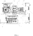
- FIG. 1 a structure of the current power module 100' is illustrated, wherein a high voltage chamber 101' and a low voltage chamber 102' of the power module 100' are arranged in parallel and next to each other, a high voltage unit 10' is located in the high voltage chamber, a low voltage unit 20' and a transformer 30' are located in the low voltage chamber 102', and the high voltage unit 10' and the transformer 30' are connected by a cable 40'. Moreover, a fan unit 50' is on a surface of the high voltage chamber 101' and the low voltage chamber 102'.
- Such structure has the following disadvantages.
- Sequential arrangment of internal structure of the module causes a large height, so that the power module is not easy to be carried.
- the high voltage chamber is deep, which lead to difficulty in connecting and fixing the cable and the optical fiber.
- mask-type housing insulation of the housing causes a large size, a heavier weight and a high cost of the module.
- the current power module product commonly has the following deficiencies.
- the power devices are arranged unreasonably, and layout of the transformer is placed obliquely, which lead to waste of space, and a low power density.
- a total wind tunnel is long, and wind resistance is large, such that improvement of heat dissipation capability of the product is limited.
- the number of cooling fins is large, and the cooling fins are scattered, such that assembly is complicated.
- Shape of the insulating housing is complicated, the mold is complicated, and accuracy of the insulating housing is low.
- An object of the invention is to provide a power module and a power conversion device, which can solve at least one or more deficiencies of the prior art, and can efficiently improve a power density of the power module while simplifying procedures of assembling and fabricating, thereby better conforming to market demand, and improving product competitiveness.
- the invention provides a power module, comprising: a primary converting unit comprising a first active device unit; a secondary converting unit comprising a second active device unit; a transformer comprising a primary unit and a secondary unit, wherein the primary unit is connected to the primary converting unit, and the secondary unit is connected to the secondary converting unit; a first heat dissipating unit on which the primary unit and the first active device unit are disposed; a second heat dissipating unit on which the secondary unit and the second active device unit are disposed; and an insulating plate comprising an insulating plate body and a semi-conducting layer disposed on a surface of the insulating plate body; wherein the primary converting unit, the primary unit and the first heat dissipating unit are located at a first side of the insulating plate, the secondary converting unit, the secondary unit and the second heat dissipating unit are located at a second side of the insulating plate, and the semi-conducting layer covers projections of
- the primary unit and the first active device unit are located at a same side of the first heat dissipating unit, and the secondary unit and the second active device unit are located at a same side of the second heat dissipating unit.
- the primary converting unit further comprises a first passive device unit
- the secondary converting unit further comprises a second passive device unit
- the first active device unit and the first passive device unit are stacked, and the second active device unit and the second passive device unit are stacked.
- the first passive device unit and the first heat dissipating unit are disposed side by side, and the second passive device unit and the second heat dissipating unit are disposed side by side.
- the primary unit and the first active device unit are located at two opposite sides of the first heat dissipating unit, and the secondary unit and the second active device unit are located at two opposite sides of the second heat dissipating unit.
- the power module further comprises: a first insulating housing inside which the primary converting unit, the first heat dissipating unit and the primary unit are disposed.
- a section of the first insulating housing is a C-shape
- the first insulating housing is spliced, or integrated with the insulating plate to form a first housing
- an outer surface of the first housing is sprayed with a zinc spraying layer except a region where the semi-conducting layer is formed.
- the zinc spraying layer is grounded.
- the power module further comprises: a second insulating housing inside which the secondary converting unit, the second heat dissipating unit and the secondary unit are disposed.
- a section of the second insulating housing is a C-shape, and the second insulating housing is spliced with the insulating plate.
- the first heat dissipating unit and/or the second heat dissipating unit are liquid-cooling heat dissipating units.
- the first heat dissipating unit and/or the second heat dissipating unit are air-cooling heat dissipating units
- the power module further comprises a fan unit correspondingly disposed at an end of the insulating plate.
- the fan unit comprises a first fan and a second fan correspondingly disposed at a first end of the insulating plate, and lactated at both sides of the insulating plate, respectively.
- the invention further provides a power conversion device, comprising: a cabinet; and a plurality of power modules as described above, arranged side by side in the cabinet.
- the phrases “one”, “a(an)”, “the”, “said” and “at least one” refer to one or more factors/components/the like.
- the terms “include”, “comprise” and “have” refer to an open and included meaning, and refer to additional factors/components/the like, in addition to the listed factors/components/the like.
- the embodiments may use relative phrases, such as, “upper” or “lower” to describe a relative relation of one signed component over another component. It shall be understood that if the signed device reverses to turn upside down, the described component on an “upper” side will become a component on a “lower” side.
- the terms “first”, “second” and the like in the claims are only used as signs, instead of numeral limitations to objects.
- a power module 100-1 in the first preferable embodiment of the invention comprises a primary converting unit 10, a secondary converting unit 20, a transformer 30, a first heat dissipating unit 41, a second heat dissipating unit 42 and an insulating plate 50.
- the primary converting unit 10 may comprise a first active device unit 11.
- the secondary converting unit 20 may comprise a second active device unit 21.
- the transformer 30 may comprise a primary unit 31 and a secondary unit 32, wherein the primary unit 31 is connected to the primary converting unit 10, and the secondary unit 32 is connected to the secondary converting unit 20.
- the primary unit 31 and the first active device unit 11 are disposed at the first heat dissipating unit 41, and the secondary unit 32 and the second active device unit 21 are disposed at the second heat dissipating unit 42.
- the insulating plate 50 may comprise an insulating plate body and a semi-conducting layer disposed on a surface of the insulating plate body.
- a semi-conducting layer (not shown) can be coated on two opposite surfaces 51 and 52 at left and right side of the insulating plate 50, respectively.
- the primary converting unit 10, the primary unit 31 and the first heat dissipating unit 41 are located at a first side (e.g., a left side) of the insulating plate 50, and the secondary converting unit 20, the secondary unit 32 and the second heat dissipating unit 42 are located at a second side (e.g., a right side) of the insulating plate 50.
- the semi-conducting layer covers projections of the transformer 30, the primary converting unit 10 and the secondary converting unit 20 on the insulating plate 50.
- the primary converting unit 10 may further comprise a first passive device unit 12, and the first active device unit 11 and the first passive device unit 12 may be stacked.
- the secondary converting unit 20 may further comprise a second passive device unit 22, and the second active device unit 21 and the second passive device unit 22 may be stacked.
- the primary unit 31 and the first active device unit 11 may be located on the same side of the first heat dissipating unit 41, as shown in FIGS. 2B , 2E and 2F .
- the secondary unit 32 and the second active device unit 21 may be located on the same side of the second heat dissipating unit 42.
- the power module 100-1 may further comprise a housing 60.
- the housing 60 may be an insulating housing, and may be a hollow rectangular structure. More preferably, the insulating plate 50 and the housing 60 are integrally formed. A hollow space of the housing 60 is divided by the insulating plate 50 into left and right accommodating spaces 610 and 620.
- the primary converting unit 10, the first heat dissipating unit 41 and the primary unit 31, for example, may form a high voltage unit HV of the power module and the high voltage unit HV is arranged in the accommodating space 610.
- the secondary converting unit 20, the second heat dissipating unit 42 and the secondary unit 32 may form a low voltage unit LV of the power module and the low voltage unit LV is arranged in the accommodating space 620.
- an outer lateral surface of the housing 60 may be sprayed with a zinc spraying layer (not shown).
- FIG. 2C it illustrates a structure of one preferable circuit of the power module according to the invention.
- the circuit comprises a transformer T, a primary converting unit at a high-voltage side, and a secondary converting unit at a low-voltage side.
- a primary side and an inductor connected thereto (a leakage inductor of the transformer in this embodiment) of the transformer T for example, form the primary unit 31 of the transformer 30 in FIG. 2B
- a secondary side of the transformer T for example, form the secondary unit 32 of the transformer 30 in FIG. 2B .
- a circuit 11-1 including a plurality of transistors and diodes and a circuit 11-2 including a plurality of transistors in the primary converting unit may be encapsulated as the first active device unit 11 of the primary converting unit 10 in FIG. 2B
- a circuit 12-1 including a plurality of capacitors and a circuit 12-2 including primary capacitors in the primary converting unit may be encapsulated as the first passive device unit 12 of the primary converting unit 10 in FIG. 2B
- a circuit including a plurality of transistors in the secondary converting unit for example, may be encapsulated as the second active device unit 21 of the secondary converting unit 20 in FIG.
- FIG. 2C only illustrates the structure of one preferable circuit of the invention, but it shall be understood that the circuit of the power module of the invention is not limited thereto, and the invention is not limited thereto.
- the first heat dissipating unit 41 and/or the second heat dissipating unit 42 may be liquid-cooling heat dissipating units.
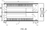
- the first heat dissipating unit 41 and/or the second heat dissipating unit 42 may be air-cooling heat dissipating units, and in this case, the power module 100-1 may further comprise a fan unit 70, as shown in FIG. 2E , and the fan unit 70 may be disposed at one end (e.g., right end) of the insulating plate 50 correspondingly.
- the fan unit 70 may comprise a first fan and a second fan disposed at a first end (e.g., a right end) of the insulating plate 50 correspondingly, and located at both sides of the insulating plate 50, respectively.
- Airflow may be generated by the fan unit 70, and may flow along an airflow direction AF in FIG. 2E to cool unit devices in the accommodating spaces 610 and 620.
- the first heat dissipating unit 41 and/or the second heat dissipating unit 42 may also be compatible with both air-cooling and liquid-cooling heat dissipation.
- a first insulating region IA1 and a second insulating region IA2 may also be formed at left and right ends of the housing 60, respectively.
- the primary converting unit 10 and the secondary converting unit 20, and the primary unit 31 and the secondary unit 32 of the transformer 30 can be arranged closely to the insulating plate 50. Therefore, requirement for electrical safety can be satisfied and a size of the power unit can be reduced. Moreover, the invention enables components to be highly matched by separating the active units from the passive units.
- the power device and the transformer of the power module in the first preferable embodiment can realize concentrated heat dissipation, and have few cooling components (in a case of liquid-cooling heat dissipation, Ingress Protection (IP) grade of the power unit can be improved), thereby simplifying assembly.
- the transformer can be pre-assembled with the heat dissipating units, and the installation is easy.
- the primary and secondary units of the transformer and the primary and secondary converting units can be assembled outside the housing, thereby simplifying connection. Shape of the insulating plate is regular, structure of the mold is simple, and accuracy is high.
- the power module in the first preferable embodiment further improves heat dissipation capability by optimizing the wind tunnel and reducing the wind resistance. Moreover, it can realize compatibility of air-cooling and liquid-cooling heat dissipation.
- the high voltage unit (as shown in FIG. 2E ) and the low voltage unit (as shown in FIG. 2E ) of the power module in the first preferable embodiment are replaced by structures shown in FIG. 3A .
- the first passive device unit 12 and the first heat dissipating unit 41 may be disposed side by side, as shown in FIG. 3A
- the second passive device unit 22 and the second heat dissipating unit 42 may also be disposed side by side (not shown).
- the power module in the second preferable embodiment may narrow a width W (as shown in FIG. 3B ) by arranging the passive device units and the heat dissipating units side by side, such that a width of the power module also can be narrowed to be suitable for a cabinet with a small width.
- a power module 100-3 in the third preferable embodiment of the invention differs from the power module 100-1 in the first preferable embodiment in that the housing 60 includes a first insulating housing 61 and a second insulating housing 62.
- a section of the first insulating housing 61 may be a C-shape
- the first insulating housing 61 may be spliced with the insulating plate 50 to form a first housing, and may also be integrated with the insulating plate 50 to form a first housing.
- a section of the second insulating housing 62 for example, may be a C-shape, and the second insulating housing 62 may be spliced with the insulating plate 50.
- the first active device unit 11 and the first passive device unit 12 of the primary converting unit, the first heat dissipating unit 41 and the primary unit 31 of the transformer may form a high voltage unit HV, and the high voltage unit HV is placed inside the first insulating housing 61, i.e., in the accommodating space 610.
- the second active device unit 21 and the second passive device unit 22 of the secondary converting unit, the second heat dissipating unit 42 and the secondary unit 32 of the transformer for example, may form a low voltage unit LV, and the low voltage unit LV is placed inside the second insulating housing 62, i.e., in the accommodating space 620.
- the power module 100-3 in the third preferable embodiment may be further sprayed with a zinc spraying layer 63 on an outer surface of the first housing except a region where the semi-conducting layer is formed.
- the zinc spraying layer 63 may be grounded.
- the power module 100-3 in the third preferable embodiment is grounded through the zinc spraying layer 63, so it is safe to touch.
- the power module 100-3 in the third preferable embodiment may also improve a partial discharge voltage of the power module.
- a power module 100-4 in the fourth preferable embodiment of the invention differs from the power module 100-1 in the first preferable embodiment in that the primary unit 31 of the transformer and the first active device unit 11 of the primary converting unit 10 are located at two opposite sides of the first heat dissipating unit 41, respectively, and the secondary unit 32 of the transformer and the second active device unit 21 of the secondary converting unit 20 are located at two opposite sides of the second heat dissipating unit 42, respectively.
- the primary converting unit 10 further comprises a first passive device unit 12, and the first active device unit 11 and the first passive device unit 12 are stacked.
- the secondary converting unit 20 further comprises a second passive device unit 22, and the second active device unit 21 and the second passive device unit 22 are stacked.
- the power module 100-4 in the fourth preferable embodiment can fully make use of two surfaces at two opposite sides of the heat dissipating unit, thereby reducing a size of the heat dissipating unit, such that a size of the insulating plate 50 coated with the semi-conducting layer can be reduced.
- FIGS. 6A and 6B illustrate a structure of a power conversion device 600 in the invention, comprising a cabinet 601 and a plurality of power modules (100-1, 100-3, or 100-4, etc.).
- the single power module for example, may be divided into left and right sides, the left side is high voltage, and the right side is low voltage.
- these power modules are arranged in parallel in the cabinet 601, and an extremely small gap is reserved among the modules after being sprayed with the zinc spraying layer and grounded, such that electrical insulation requirement can be satisfied, and a volume of the cabinet can be reduced.
Landscapes
- Engineering & Computer Science (AREA)
- Microelectronics & Electronic Packaging (AREA)
- Physics & Mathematics (AREA)
- Thermal Sciences (AREA)
- Power Engineering (AREA)
- Dc-Dc Converters (AREA)
Abstract
Description
- The invention relates to the technical field of electric power, and particularly to a power module and a power conversion device.
- With gradual growth of market demand for electric vehicles, production and sales of electric vehicles are continuously increased, and have a trendency to exceed those of the traditional vehicles. Moreover, demand for charging facilities which function as important accessories, is also increasing rapidly, and performance required by the market is also continuously improved.
- Meanwhile, since our country classifies data center into new infrastructure, rapid construction of big data center, which functions as infrastructure of intelligent economic base, becomes an inevitably demand. The IT investment of Chinese data center in 2019 has reached RMB 369.81 billion, and it is predicted that investment in 2020 will be increased by 12.7%, and reach RMB 416.68 billion. As is predicted, investment in 2025 will reach RMB 707.09 billion, so demand for power equipment of the data center also faces explosive growth.
- As a core compoment in the power equipment of electric vehicles and data centers, the power module also faces greater challenge and higher requirement. As shown in
FIG. 1 , a structure of the current power module 100' is illustrated, wherein a high voltage chamber 101' and a low voltage chamber 102' of the power module 100' are arranged in parallel and next to each other, a high voltage unit 10' is located in the high voltage chamber, a low voltage unit 20' and a transformer 30' are located in the low voltage chamber 102', and the high voltage unit 10' and the transformer 30' are connected by a cable 40'. Moreover, a fan unit 50' is on a surface of the high voltage chamber 101' and the low voltage chamber 102'. Such structure has the following disadvantages. (1) Sequential arrangment of internal structure of the module causes a large height, so that the power module is not easy to be carried. The high voltage chamber is deep, which lead to difficulty in connecting and fixing the cable and the optical fiber. (2) mask-type housing insulation of the housing causes a large size, a heavier weight and a high cost of the module. - In addition, the current power module product commonly has the following deficiencies. (1) The power devices are arranged unreasonably, and layout of the transformer is placed obliquely, which lead to waste of space, and a low power density. (2) A total wind tunnel is long, and wind resistance is large, such that improvement of heat dissipation capability of the product is limited. (3) The number of cooling fins is large, and the cooling fins are scattered, such that assembly is complicated. (4) Shape of the insulating housing is complicated, the mold is complicated, and accuracy of the insulating housing is low.
- An object of the invention is to provide a power module and a power conversion device, which can solve at least one or more deficiencies of the prior art, and can efficiently improve a power density of the power module while simplifying procedures of assembling and fabricating, thereby better conforming to market demand, and improving product competitiveness.
- To realize the object, the invention provides a power module, comprising: a primary converting unit comprising a first active device unit; a secondary converting unit comprising a second active device unit; a transformer comprising a primary unit and a secondary unit, wherein the primary unit is connected to the primary converting unit, and the secondary unit is connected to the secondary converting unit; a first heat dissipating unit on which the primary unit and the first active device unit are disposed; a second heat dissipating unit on which the secondary unit and the second active device unit are disposed; and an insulating plate comprising an insulating plate body and a semi-conducting layer disposed on a surface of the insulating plate body; wherein the primary converting unit, the primary unit and the first heat dissipating unit are located at a first side of the insulating plate, the secondary converting unit, the secondary unit and the second heat dissipating unit are located at a second side of the insulating plate, and the semi-conducting layer covers projections of the transformer, the primary converting unit and the secondary converting unit on the insulating plate.
- In one embodiment of the invention, the primary unit and the first active device unit are located at a same side of the first heat dissipating unit, and the secondary unit and the second active device unit are located at a same side of the second heat dissipating unit.
- In one embodiment of the invention, the primary converting unit further comprises a first passive device unit, and the secondary converting unit further comprises a second passive device unit.
- In one embodiment of the invention, the first active device unit and the first passive device unit are stacked, and the second active device unit and the second passive device unit are stacked.
- In one embodiment of the invention, the first passive device unit and the first heat dissipating unit are disposed side by side, and the second passive device unit and the second heat dissipating unit are disposed side by side.
- In one embodiment of the invention, the primary unit and the first active device unit are located at two opposite sides of the first heat dissipating unit, and the secondary unit and the second active device unit are located at two opposite sides of the second heat dissipating unit.
- In one embodiment of the invention, the power module further comprises: a first insulating housing inside which the primary converting unit, the first heat dissipating unit and the primary unit are disposed.
- In one embodiment of the invention, a section of the first insulating housing is a C-shape, the first insulating housing is spliced, or integrated with the insulating plate to form a first housing, and an outer surface of the first housing is sprayed with a zinc spraying layer except a region where the semi-conducting layer is formed.
- In one embodiment of the invention, the zinc spraying layer is grounded.
- In one embodiment of the invention, the power module further comprises: a second insulating housing inside which the secondary converting unit, the second heat dissipating unit and the secondary unit are disposed.
- In one embodiment of the invention, a section of the second insulating housing is a C-shape, and the second insulating housing is spliced with the insulating plate.
- In one embodiment of the invention, the first heat dissipating unit and/or the second heat dissipating unit are liquid-cooling heat dissipating units.
- In one embodiment of the invention, the first heat dissipating unit and/or the second heat dissipating unit are air-cooling heat dissipating units, and the power module further comprises a fan unit correspondingly disposed at an end of the insulating plate.
- In one embodiment of the invention, the fan unit comprises a first fan and a second fan correspondingly disposed at a first end of the insulating plate, and lactated at both sides of the insulating plate, respectively.
- To realize the object, the invention further provides a power conversion device, comprising: a cabinet; and a plurality of power modules as described above, arranged side by side in the cabinet.
- The exemplary embodiments will be described in detail with reference to the accompanying drawings, through which the above and other features and advantages of the invention will become more apparent.
-
FIG. 1 is a structural diagram of the current power module. -
FIG. 2A is a structural diagram of a power module in the first preferable embodiment of the invention. -
FIG. 2B is a schematic diagram of an assembled structure of the power module ofFIG. 2A after removing a housing. -
FIG. 2C is a structural diagram of one preferable circuit of the power module according to the invention. -
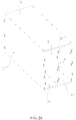
FIG. 2D is a structural diagram of the housing in the power module ofFIG. 2A . -
FIG. 2E is a schematic diagram of a sectional structure, viewing from top, of the power module ofFIG. 2A , wherein one end of the power module is further provided with a fan unit. -
FIG. 2F is a structural diagram of a primary converting unit, a primary unit of a transformer and a first heat dissipating unit after being assembled, wherein a first active device unit and a first passive device unit of the primary converting unit are stacked. -
FIG. 3A is a structural diagram of a primary converting unit, a primary unit of a transformer and a first heat dissipating unit of a power module in the second preferable embodiment of the invention after being assembled, wherein a first active device unit and a first passive device unit of the primary converting unit are disposed side by side. -
FIG. 3B is a side view ofFIG. 3A . -
FIG. 4A is a structural diagram of a power module in the third preferable embodiment of the invention. -
FIG. 4B is a structural diagram of a housing in the power module ofFIG. 4A . -
FIG. 5A is a structural diagram of a power module in the fourth preferable embodiment of the invention. -
FIG. 5B is a structural diagram of a primary converting unit, a primary unit of a transformer and a first heat dissipating unit in the power module ofFIG. 5A after being assembled, wherein a first active device unit of the primary converting unit and the primary unit of the transformer are located on two opposite sides of the first heat dissipating unit. -
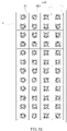
FIG. 6A is a structural diagram of a preferable power conversion device according to the invention. -
FIG. 6B is a sectional view of a lateral surface of the power conversion device ofFIG. 6A . - The exemplary embodiments will now be described more fully with reference to the accompanying drawings. However, the exemplary embodiments can be implemented in various forms and shall not be understood as being limited to the embodiments set forth herein; on the contrary, these embodiments are provided so that this invention will be thorough and complete, and the conception of exemplary embodiments will be fully conveyed to those skilled in the art. In the drawings, the same reference sign denotes the same or similar structure, so their detailed description will be omitted.
- When factors/components/the like described and/or illustrated here are introduced, the phrases "one", "a(an)", "the", "said" and "at least one" refer to one or more factors/components/the like. The terms "include", "comprise" and "have" refer to an open and included meaning, and refer to additional factors/components/the like, in addition to the listed factors/components/the like. The embodiments may use relative phrases, such as, "upper" or "lower" to describe a relative relation of one signed component over another component. It shall be understood that if the signed device reverses to turn upside down, the described component on an "upper" side will become a component on a "lower" side. In addition, the terms "first", "second" and the like in the claims are only used as signs, instead of numeral limitations to objects.
- As shown in
FIGS. 2A-2E , a power module 100-1 in the first preferable embodiment of the invention comprises a primary convertingunit 10, a secondary convertingunit 20, atransformer 30, a firstheat dissipating unit 41, a secondheat dissipating unit 42 and an insulatingplate 50. The primary convertingunit 10 may comprise a firstactive device unit 11. The secondary convertingunit 20 may comprise a secondactive device unit 21. Thetransformer 30 may comprise aprimary unit 31 and asecondary unit 32, wherein theprimary unit 31 is connected to the primary convertingunit 10, and thesecondary unit 32 is connected to the secondary convertingunit 20. Theprimary unit 31 and the firstactive device unit 11 are disposed at the firstheat dissipating unit 41, and thesecondary unit 32 and the secondactive device unit 21 are disposed at the secondheat dissipating unit 42. The insulatingplate 50 may comprise an insulating plate body and a semi-conducting layer disposed on a surface of the insulating plate body. For example, referring toFIGS. 2A , a semi-conducting layer (not shown) can be coated on twoopposite surfaces plate 50, respectively. The primary convertingunit 10, theprimary unit 31 and the firstheat dissipating unit 41 are located at a first side (e.g., a left side) of the insulatingplate 50, and the secondary convertingunit 20, thesecondary unit 32 and the secondheat dissipating unit 42 are located at a second side (e.g., a right side) of the insulatingplate 50. Moreover, the semi-conducting layer covers projections of thetransformer 30, the primary convertingunit 10 and the secondary convertingunit 20 on the insulatingplate 50. - As shown in
FIGS. 2B ,2E and2F , in this embodiment, the primary convertingunit 10 may further comprise a firstpassive device unit 12, and the firstactive device unit 11 and the firstpassive device unit 12 may be stacked. The secondary convertingunit 20 may further comprise a secondpassive device unit 22, and the secondactive device unit 21 and the secondpassive device unit 22 may be stacked. - Preferably, the
primary unit 31 and the firstactive device unit 11 may be located on the same side of the firstheat dissipating unit 41, as shown inFIGS. 2B ,2E and2F . Thesecondary unit 32 and the secondactive device unit 21 may be located on the same side of the secondheat dissipating unit 42. - In this embodiment, the power module 100-1 may further comprise a
housing 60. Thehousing 60, for example, may be an insulating housing, and may be a hollow rectangular structure. More preferably, the insulatingplate 50 and thehousing 60 are integrally formed. A hollow space of thehousing 60 is divided by the insulatingplate 50 into left and rightaccommodating spaces unit 10, the firstheat dissipating unit 41 and theprimary unit 31, for example, may form a high voltage unit HV of the power module and the high voltage unit HV is arranged in theaccommodating space 610. The secondary convertingunit 20, the secondheat dissipating unit 42 and thesecondary unit 32, for example, may form a low voltage unit LV of the power module and the low voltage unit LV is arranged in theaccommodating space 620. Preferably, an outer lateral surface of thehousing 60 may be sprayed with a zinc spraying layer (not shown). - As shown in
FIG. 2C , it illustrates a structure of one preferable circuit of the power module according to the invention. The circuit comprises a transformer T, a primary converting unit at a high-voltage side, and a secondary converting unit at a low-voltage side. Referring toFIG. 2B , a primary side and an inductor connected thereto (a leakage inductor of the transformer in this embodiment) of the transformer T, for example, form theprimary unit 31 of thetransformer 30 inFIG. 2B , and a secondary side of the transformer T, for example, form thesecondary unit 32 of thetransformer 30 inFIG. 2B . A circuit 11-1 including a plurality of transistors and diodes and a circuit 11-2 including a plurality of transistors in the primary converting unit, for example, may be encapsulated as the firstactive device unit 11 of the primary convertingunit 10 inFIG. 2B , and a circuit 12-1 including a plurality of capacitors and a circuit 12-2 including primary capacitors in the primary converting unit, for example, may be encapsulated as the firstpassive device unit 12 of the primary convertingunit 10 inFIG. 2B . A circuit including a plurality of transistors in the secondary converting unit, for example, may be encapsulated as the secondactive device unit 21 of the secondary convertingunit 20 inFIG. 2B , and a circuit including one capacitor in the secondary converting unit, for example, may be encapsulated as the secondpassive device unit 22 of the secondary convertingunit 20 inFIG. 2B .FIG. 2C only illustrates the structure of one preferable circuit of the invention, but it shall be understood that the circuit of the power module of the invention is not limited thereto, and the invention is not limited thereto. - In this embodiment, the first
heat dissipating unit 41 and/or the secondheat dissipating unit 42, for example, may be liquid-cooling heat dissipating units. In other embodiments, the firstheat dissipating unit 41 and/or the secondheat dissipating unit 42, for example, may be air-cooling heat dissipating units, and in this case, the power module 100-1 may further comprise afan unit 70, as shown inFIG. 2E , and thefan unit 70 may be disposed at one end (e.g., right end) of the insulatingplate 50 correspondingly. Preferably, thefan unit 70 may comprise a first fan and a second fan disposed at a first end (e.g., a right end) of the insulatingplate 50 correspondingly, and located at both sides of the insulatingplate 50, respectively. Airflow may be generated by thefan unit 70, and may flow along an airflow direction AF inFIG. 2E to cool unit devices in theaccommodating spaces heat dissipating unit 41 and/or the secondheat dissipating unit 42 may also be compatible with both air-cooling and liquid-cooling heat dissipation. - In this embodiment, as shown in
FIG. 2E , after the high voltage unit HV and the low voltage unit LV are assembled with thehousing 60, a first insulating region IA1 and a second insulating region IA2 may also be formed at left and right ends of thehousing 60, respectively. - By sharing the insulating
plate 50 coated with a semi-conducting layer, the primary convertingunit 10 and the secondary convertingunit 20, and theprimary unit 31 and thesecondary unit 32 of thetransformer 30 can be arranged closely to the insulatingplate 50. Therefore, requirement for electrical safety can be satisfied and a size of the power unit can be reduced. Moreover, the invention enables components to be highly matched by separating the active units from the passive units. - The power device and the transformer of the power module in the first preferable embodiment can realize concentrated heat dissipation, and have few cooling components (in a case of liquid-cooling heat dissipation, Ingress Protection (IP) grade of the power unit can be improved), thereby simplifying assembly. Moreover, the transformer can be pre-assembled with the heat dissipating units, and the installation is easy. The primary and secondary units of the transformer and the primary and secondary converting units can be assembled outside the housing, thereby simplifying connection. Shape of the insulating plate is regular, structure of the mold is simple, and accuracy is high.
- The power module in the first preferable embodiment further improves heat dissipation capability by optimizing the wind tunnel and reducing the wind resistance. Moreover, it can realize compatibility of air-cooling and liquid-cooling heat dissipation.
- In a power module 100-2 of the second preferable embodiment of the invention, the high voltage unit (as shown in
FIG. 2E ) and the low voltage unit (as shown inFIG. 2E ) of the power module in the first preferable embodiment, for example, are replaced by structures shown inFIG. 3A . For example, the firstpassive device unit 12 and the firstheat dissipating unit 41 may be disposed side by side, as shown inFIG. 3A , and the secondpassive device unit 22 and the secondheat dissipating unit 42 may also be disposed side by side (not shown). - The power module in the second preferable embodiment may narrow a width W (as shown in
FIG. 3B ) by arranging the passive device units and the heat dissipating units side by side, such that a width of the power module also can be narrowed to be suitable for a cabinet with a small width. - As shown in
FIGS. 4A and4B , a power module 100-3 in the third preferable embodiment of the invention differs from the power module 100-1 in the first preferable embodiment in that thehousing 60 includes a first insulatinghousing 61 and a second insulatinghousing 62. A section of the first insulatinghousing 61, for example, may be a C-shape, the first insulatinghousing 61 may be spliced with the insulatingplate 50 to form a first housing, and may also be integrated with the insulatingplate 50 to form a first housing. A section of the second insulatinghousing 62, for example, may be a C-shape, and the second insulatinghousing 62 may be spliced with the insulatingplate 50. The firstactive device unit 11 and the firstpassive device unit 12 of the primary converting unit, the firstheat dissipating unit 41 and theprimary unit 31 of the transformer, for example, may form a high voltage unit HV, and the high voltage unit HV is placed inside the first insulatinghousing 61, i.e., in theaccommodating space 610. The secondactive device unit 21 and the secondpassive device unit 22 of the secondary converting unit, the secondheat dissipating unit 42 and thesecondary unit 32 of the transformer, for example, may form a low voltage unit LV, and the low voltage unit LV is placed inside the second insulatinghousing 62, i.e., in theaccommodating space 620. - Preferably, the power module 100-3 in the third preferable embodiment may be further sprayed with a
zinc spraying layer 63 on an outer surface of the first housing except a region where the semi-conducting layer is formed. Thezinc spraying layer 63 may be grounded. - The power module 100-3 in the third preferable embodiment is grounded through the
zinc spraying layer 63, so it is safe to touch. The power module 100-3 in the third preferable embodiment may also improve a partial discharge voltage of the power module. - As shown in
FIGS. 5A and5B , a power module 100-4 in the fourth preferable embodiment of the invention differs from the power module 100-1 in the first preferable embodiment in that theprimary unit 31 of the transformer and the firstactive device unit 11 of the primary convertingunit 10 are located at two opposite sides of the firstheat dissipating unit 41, respectively, and thesecondary unit 32 of the transformer and the secondactive device unit 21 of the secondary convertingunit 20 are located at two opposite sides of the secondheat dissipating unit 42, respectively. - In this embodiment, the primary converting
unit 10 further comprises a firstpassive device unit 12, and the firstactive device unit 11 and the firstpassive device unit 12 are stacked. The secondary convertingunit 20 further comprises a secondpassive device unit 22, and the secondactive device unit 21 and the secondpassive device unit 22 are stacked. - The power module 100-4 in the fourth preferable embodiment can fully make use of two surfaces at two opposite sides of the heat dissipating unit, thereby reducing a size of the heat dissipating unit, such that a size of the insulating
plate 50 coated with the semi-conducting layer can be reduced. -
FIGS. 6A and6B illustrate a structure of apower conversion device 600 in the invention, comprising acabinet 601 and a plurality of power modules (100-1, 100-3, or 100-4, etc.). The single power module, for example, may be divided into left and right sides, the left side is high voltage, and the right side is low voltage. Moreover, these power modules are arranged in parallel in thecabinet 601, and an extremely small gap is reserved among the modules after being sprayed with the zinc spraying layer and grounded, such that electrical insulation requirement can be satisfied, and a volume of the cabinet can be reduced.
Claims (17)
- A power module (100-1, 100-2, 100-3, 100-4), comprising:a primary converting unit (10) comprising a first active device unit (11);a secondary converting unit (20) comprising a second active device unit (21);a transformer (30) comprising a primary unit (31) and a secondary unit (32), wherein the primary unit (31) is connected to the primary converting unit (10), and the secondary unit (32) is connected to the secondary converting unit (20);a first heat dissipating unit (41) on which the primary unit (31) and the first active device unit (11) are disposed;a second heat dissipating unit (42) on which the secondary unit (32) and the second active device unit (21) are disposed; andan insulating plate (50) comprising an insulating plate body and a semi-conducting layer disposed on a surface of the insulating plate body; whereinthe primary converting unit (10), the primary unit (31) and the first heat dissipating unit (41) are located at a first side of the insulating plate (50),the secondary converting unit (20), the secondary unit (32) and the second heat dissipating unit (42) are located at a second side of the insulating plate (50), andthe semi-conducting layer covers projections of the transformer (30), the primary converting unit (10) and the secondary converting unit (20) on the insulating plate (50).
- The power module according to claim 1, wherein the primary unit (31) and the first active device unit (11) are located at a same side of the first heat dissipating unit (41), and the secondary unit (32) and the second active device unit (21) are located at a same side of the second heat dissipating unit (42).
- The power module according to claim 2, wherein the primary converting unit (10) further comprises a first passive device unit (12), and the secondary converting unit (20) further comprises a second passive device unit (22).
- The power module according to claim 3, wherein the first active device unit (11) and the first passive device unit (12) are stacked, and the second active device unit (21) and the second passive device unit (22) are stacked.
- The power module according to claim 3, wherein the first passive device unit (12) and the first heat dissipating unit (41) are disposed side by side, and the second passive device unit (22) and the second heat dissipating unit (42) are disposed side by side.
- The power module according to claim 1, wherein the primary unit (31) and the first active device unit (11) are located at two opposite sides of the first heat dissipating unit (41), and the secondary unit (32) and the second active device unit (21) are located at two opposite sides of the second heat dissipating unit (42).
- The power module according to claim 6, wherein the primary converting unit (10) further comprises a first passive device unit (12), and the secondary converting unit (20) further comprises a second passive device unit (22).
- The power module according to claim 7, wherein the first active device unit (11) and the first passive device unit (12) are stacked, and the second active device unit (21) and the second passive device unit (22) are stacked.
- The power module according to any one of claims 1 to 8, further comprising:
a first insulating housing (61) inside which the primary converting unit (10), the first heat dissipating unit (41) and the primary unit (31) are disposed. - The power module according to claim 9, wherein a section of the first insulating housing (61) is a C-shape, the first insulating housing (61) is spliced, or integrated with the insulating plate (50) to form a first housing, and an outer surface of the first housing is sprayed with a zinc spraying layer except a region where the semi-conducting layer is formed.
- The power module according to claim 10, wherein the zinc spraying layer is grounded.
- The power module according to claim 10, further comprising:
a second insulating housing (62) inside which the secondary converting unit (20), the second heat dissipating unit (42) and the secondary unit (32) are disposed. - The power module according to claim 12, wherein a section of the second insulating housing (62) is a C-shape, and the second insulating housing (62) is spliced with the insulating plate (50).
- The power module according to claim 1, wherein the first heat dissipating unit (41) and/or the second heat dissipating unit (42) are liquid-cooling heat dissipating units.
- The power module according to claim 1, wherein the first heat dissipating unit (41) and/or the second heat dissipating unit (42) are air-cooling heat dissipating units, and the power module further comprises a fan unit correspondingly disposed at an end of the insulating plate (50).
- The power module according to claim 15, wherein the fan unit comprises a first fan and a second fan correspondingly disposed at a first end of the insulating plate (50), and lactated at both sides of the insulating plate (50), respectively.
- A power conversion device (600), comprising:a cabinet (601); anda plurality of power modules (100-1, 100-2, 100-3, 100-4) according to claim 1, arranged in the cabinet side by side.
Applications Claiming Priority (1)
| Application Number | Priority Date | Filing Date | Title |
|---|---|---|---|
| CN202011231927.8A CN114465445B (en) | 2020-11-06 | 2020-11-06 | Power module and power conversion device |
Publications (2)
| Publication Number | Publication Date |
|---|---|
| EP4009753A1 true EP4009753A1 (en) | 2022-06-08 |
| EP4009753B1 EP4009753B1 (en) | 2023-08-30 |
Family
ID=78211959
Family Applications (1)
| Application Number | Title | Priority Date | Filing Date |
|---|---|---|---|
| EP21202667.8A Active EP4009753B1 (en) | 2020-11-06 | 2021-10-14 | Power module and power conversion device |
Country Status (3)
| Country | Link |
|---|---|
| US (1) | US11757363B2 (en) |
| EP (1) | EP4009753B1 (en) |
| CN (1) | CN114465445B (en) |
Cited By (2)
| Publication number | Priority date | Publication date | Assignee | Title |
|---|---|---|---|---|
| EP4312474A1 (en) * | 2022-07-26 | 2024-01-31 | Delta Electronics (Shanghai) Co., Ltd. | Shielded insulating shell and electronic device |
| EP4394821A1 (en) * | 2022-12-27 | 2024-07-03 | Delta Electronics (Shanghai) Co., Ltd. | Power module |
Families Citing this family (3)
| Publication number | Priority date | Publication date | Assignee | Title |
|---|---|---|---|---|
| CN117098348A (en) * | 2022-05-11 | 2023-11-21 | 台达电子工业股份有限公司 | Load-bearing structure of high and low voltage conversion circuit |
| US20240164071A1 (en) * | 2022-11-10 | 2024-05-16 | Caterpillar Inc. | Power electronic systems packaged using common heat sink and enclosure |
| IT202200026742A1 (en) * | 2022-12-23 | 2024-06-23 | Friem S P A | ELECTRONIC POWER CONVERTER APPARATUS COMPRISING OVERLAP CONVERTER MODULES AND A FORCED VENTILATION COOLING UNIT |
Citations (4)
| Publication number | Priority date | Publication date | Assignee | Title |
|---|---|---|---|---|
| CN101710793A (en) * | 2009-10-27 | 2010-05-19 | 成都汇能高科电器有限公司 | High-frequency power supply device for uniformly outputting multiple groups of currents |
| US20170207607A1 (en) * | 2016-01-20 | 2017-07-20 | Lsis Co., Ltd. | Distributing panel |
| EP3618206A1 (en) * | 2018-08-30 | 2020-03-04 | Delta Electronics, Inc. | Power supply system |
| CN110890831A (en) * | 2018-09-07 | 2020-03-17 | 中车株洲电力机车研究所有限公司 | High-voltage module for power electronic traction transformer |
Family Cites Families (8)
| Publication number | Priority date | Publication date | Assignee | Title |
|---|---|---|---|---|
| JP4922840B2 (en) * | 2007-06-05 | 2012-04-25 | 株式会社日立製作所 | Switching power supply |
| US20090267466A1 (en) * | 2008-04-28 | 2009-10-29 | Meter Devices Company, Inc. | Primary enclosure for electric power meters |
| US8000052B2 (en) * | 2008-08-11 | 2011-08-16 | International Business Machines Corporation | Cartridge refresh and verify |
| ATE515780T1 (en) * | 2008-09-26 | 2011-07-15 | Bruker Biospin Sa | HIGH VOLTAGE UP DRY POWER TRANSFORMER AND POWER SUPPLY UNIT WITH AT LEAST ONE OF THESE TRANSFORMERS |
| CN106953502B (en) | 2016-01-05 | 2020-06-09 | 特变电工新疆新能源股份有限公司 | Electric energy router |
| KR102047890B1 (en) * | 2019-02-18 | 2019-12-02 | 주식회사 디텍 | LLC Resonant Power Supply |
| CN210380629U (en) * | 2019-07-29 | 2020-04-21 | 广东安朴电力技术有限公司 | Power electronic transformer power module heat radiation structure and power module |
| CN210669866U (en) * | 2019-10-31 | 2020-06-02 | 台达电子企业管理(上海)有限公司 | Power module |
-
2020
- 2020-11-06 CN CN202011231927.8A patent/CN114465445B/en active Active
-
2021
- 2021-09-28 US US17/449,090 patent/US11757363B2/en active Active
- 2021-10-14 EP EP21202667.8A patent/EP4009753B1/en active Active
Patent Citations (4)
| Publication number | Priority date | Publication date | Assignee | Title |
|---|---|---|---|---|
| CN101710793A (en) * | 2009-10-27 | 2010-05-19 | 成都汇能高科电器有限公司 | High-frequency power supply device for uniformly outputting multiple groups of currents |
| US20170207607A1 (en) * | 2016-01-20 | 2017-07-20 | Lsis Co., Ltd. | Distributing panel |
| EP3618206A1 (en) * | 2018-08-30 | 2020-03-04 | Delta Electronics, Inc. | Power supply system |
| CN110890831A (en) * | 2018-09-07 | 2020-03-17 | 中车株洲电力机车研究所有限公司 | High-voltage module for power electronic traction transformer |
Cited By (2)
| Publication number | Priority date | Publication date | Assignee | Title |
|---|---|---|---|---|
| EP4312474A1 (en) * | 2022-07-26 | 2024-01-31 | Delta Electronics (Shanghai) Co., Ltd. | Shielded insulating shell and electronic device |
| EP4394821A1 (en) * | 2022-12-27 | 2024-07-03 | Delta Electronics (Shanghai) Co., Ltd. | Power module |
Also Published As
| Publication number | Publication date |
|---|---|
| US11757363B2 (en) | 2023-09-12 |
| CN114465445A (en) | 2022-05-10 |
| US20220149743A1 (en) | 2022-05-12 |
| EP4009753B1 (en) | 2023-08-30 |
| CN114465445B (en) | 2024-05-14 |
Similar Documents
| Publication | Publication Date | Title |
|---|---|---|
| EP4009753B1 (en) | Power module and power conversion device | |
| CN208781901U (en) | Secondary battery module and secondary battery cooling frame | |
| JP6696869B2 (en) | Quick charger | |
| EP2220663B1 (en) | Heat dissipating means for circuit-breaker and circuit-breaker with such heat dissipating means | |
| US11683900B2 (en) | Power conversion system | |
| US11158998B1 (en) | Heat sink for power supply panel | |
| RU2744933C2 (en) | Planar transformer layer, assembly of layers for planar transformer and planar transformer | |
| JPH08294266A (en) | Power module and power converter | |
| CN113329587A (en) | Power conversion device | |
| CN220914233U (en) | Power module, vehicle-mounted charging device, integrated controller and vehicle | |
| US12407268B2 (en) | Power module of isolated converter | |
| CN112440705A (en) | Power assembly | |
| WO2019245148A1 (en) | Converter | |
| JP2018042337A (en) | Power converter | |
| CN113014067A (en) | Power module assembly and converter | |
| WO2024198729A1 (en) | Power device | |
| US20250381866A1 (en) | On-board charger and vehicle | |
| CN102017039B (en) | Heat dissipating means for circuit-breaker and circuit-breaker with such heat dissipating means | |
| WO2023043249A1 (en) | Converter | |
| JP2023502205A (en) | converter | |
| CN222507304U (en) | A high thermal conductivity inductive magnetic device and power supply equipment | |
| KR102769790B1 (en) | A DC-DC converter device for common power control for high-voltage hydrogen fuel cell vehicles and electric vehicles with fanless air cooling function | |
| CN222995488U (en) | Battery pack cover, first battery pack, second battery pack and electrical equipment | |
| CN222213875U (en) | Magnetic element and electrical equipment | |
| CN221126320U (en) | Extension socket structure of integrated charger |
Legal Events
| Date | Code | Title | Description |
|---|---|---|---|
| PUAI | Public reference made under article 153(3) epc to a published international application that has entered the european phase |
Free format text: ORIGINAL CODE: 0009012 |
|
| STAA | Information on the status of an ep patent application or granted ep patent |
Free format text: STATUS: THE APPLICATION HAS BEEN PUBLISHED |
|
| AK | Designated contracting states |
Kind code of ref document: A1 Designated state(s): AL AT BE BG CH CY CZ DE DK EE ES FI FR GB GR HR HU IE IS IT LI LT LU LV MC MK MT NL NO PL PT RO RS SE SI SK SM TR |
|
| STAA | Information on the status of an ep patent application or granted ep patent |
Free format text: STATUS: REQUEST FOR EXAMINATION WAS MADE |
|
| 17P | Request for examination filed |
Effective date: 20221122 |
|
| RBV | Designated contracting states (corrected) |
Designated state(s): AL AT BE BG CH CY CZ DE DK EE ES FI FR GB GR HR HU IE IS IT LI LT LU LV MC MK MT NL NO PL PT RO RS SE SI SK SM TR |
|
| GRAP | Despatch of communication of intention to grant a patent |
Free format text: ORIGINAL CODE: EPIDOSNIGR1 |
|
| STAA | Information on the status of an ep patent application or granted ep patent |
Free format text: STATUS: GRANT OF PATENT IS INTENDED |
|
| RIC1 | Information provided on ipc code assigned before grant |
Ipc: H05K 7/20 20060101ALI20230308BHEP Ipc: H05K 7/14 20060101AFI20230308BHEP |
|
| INTG | Intention to grant announced |
Effective date: 20230329 |
|
| GRAS | Grant fee paid |
Free format text: ORIGINAL CODE: EPIDOSNIGR3 |
|
| GRAA | (expected) grant |
Free format text: ORIGINAL CODE: 0009210 |
|
| STAA | Information on the status of an ep patent application or granted ep patent |
Free format text: STATUS: THE PATENT HAS BEEN GRANTED |
|
| AK | Designated contracting states |
Kind code of ref document: B1 Designated state(s): AL AT BE BG CH CY CZ DE DK EE ES FI FR GB GR HR HU IE IS IT LI LT LU LV MC MK MT NL NO PL PT RO RS SE SI SK SM TR |
|
| P01 | Opt-out of the competence of the unified patent court (upc) registered |
Effective date: 20230721 |
|
| REG | Reference to a national code |
Ref country code: GB Ref legal event code: FG4D |
|
| REG | Reference to a national code |
Ref country code: CH Ref legal event code: EP |
|
| REG | Reference to a national code |
Ref country code: DE Ref legal event code: R096 Ref document number: 602021004697 Country of ref document: DE |
|
| RAP4 | Party data changed (patent owner data changed or rights of a patent transferred) |
Owner name: DELTA ELECTRONICS (SHANGHAI) CO., LTD. |
|
| REG | Reference to a national code |
Ref country code: IE Ref legal event code: FG4D |
|
| REG | Reference to a national code |
Ref country code: NL Ref legal event code: FP |
|
| REG | Reference to a national code |
Ref country code: LT Ref legal event code: MG9D |
|
| REG | Reference to a national code |
Ref country code: AT Ref legal event code: MK05 Ref document number: 1607169 Country of ref document: AT Kind code of ref document: T Effective date: 20230830 |
|
| PG25 | Lapsed in a contracting state [announced via postgrant information from national office to epo] |
Ref country code: GR Free format text: LAPSE BECAUSE OF FAILURE TO SUBMIT A TRANSLATION OF THE DESCRIPTION OR TO PAY THE FEE WITHIN THE PRESCRIBED TIME-LIMIT Effective date: 20231201 |
|
| PG25 | Lapsed in a contracting state [announced via postgrant information from national office to epo] |
Ref country code: IS Free format text: LAPSE BECAUSE OF FAILURE TO SUBMIT A TRANSLATION OF THE DESCRIPTION OR TO PAY THE FEE WITHIN THE PRESCRIBED TIME-LIMIT Effective date: 20231230 |
|
| PG25 | Lapsed in a contracting state [announced via postgrant information from national office to epo] |
Ref country code: SE Free format text: LAPSE BECAUSE OF FAILURE TO SUBMIT A TRANSLATION OF THE DESCRIPTION OR TO PAY THE FEE WITHIN THE PRESCRIBED TIME-LIMIT Effective date: 20230830 Ref country code: RS Free format text: LAPSE BECAUSE OF FAILURE TO SUBMIT A TRANSLATION OF THE DESCRIPTION OR TO PAY THE FEE WITHIN THE PRESCRIBED TIME-LIMIT Effective date: 20230830 Ref country code: NO Free format text: LAPSE BECAUSE OF FAILURE TO SUBMIT A TRANSLATION OF THE DESCRIPTION OR TO PAY THE FEE WITHIN THE PRESCRIBED TIME-LIMIT Effective date: 20231130 Ref country code: LV Free format text: LAPSE BECAUSE OF FAILURE TO SUBMIT A TRANSLATION OF THE DESCRIPTION OR TO PAY THE FEE WITHIN THE PRESCRIBED TIME-LIMIT Effective date: 20230830 Ref country code: LT Free format text: LAPSE BECAUSE OF FAILURE TO SUBMIT A TRANSLATION OF THE DESCRIPTION OR TO PAY THE FEE WITHIN THE PRESCRIBED TIME-LIMIT Effective date: 20230830 Ref country code: IS Free format text: LAPSE BECAUSE OF FAILURE TO SUBMIT A TRANSLATION OF THE DESCRIPTION OR TO PAY THE FEE WITHIN THE PRESCRIBED TIME-LIMIT Effective date: 20231230 Ref country code: HR Free format text: LAPSE BECAUSE OF FAILURE TO SUBMIT A TRANSLATION OF THE DESCRIPTION OR TO PAY THE FEE WITHIN THE PRESCRIBED TIME-LIMIT Effective date: 20230830 Ref country code: GR Free format text: LAPSE BECAUSE OF FAILURE TO SUBMIT A TRANSLATION OF THE DESCRIPTION OR TO PAY THE FEE WITHIN THE PRESCRIBED TIME-LIMIT Effective date: 20231201 Ref country code: FI Free format text: LAPSE BECAUSE OF FAILURE TO SUBMIT A TRANSLATION OF THE DESCRIPTION OR TO PAY THE FEE WITHIN THE PRESCRIBED TIME-LIMIT Effective date: 20230830 Ref country code: AT Free format text: LAPSE BECAUSE OF FAILURE TO SUBMIT A TRANSLATION OF THE DESCRIPTION OR TO PAY THE FEE WITHIN THE PRESCRIBED TIME-LIMIT Effective date: 20230830 |
|
| PG25 | Lapsed in a contracting state [announced via postgrant information from national office to epo] |
Ref country code: PL Free format text: LAPSE BECAUSE OF FAILURE TO SUBMIT A TRANSLATION OF THE DESCRIPTION OR TO PAY THE FEE WITHIN THE PRESCRIBED TIME-LIMIT Effective date: 20230830 |
|
| PG25 | Lapsed in a contracting state [announced via postgrant information from national office to epo] |
Ref country code: ES Free format text: LAPSE BECAUSE OF FAILURE TO SUBMIT A TRANSLATION OF THE DESCRIPTION OR TO PAY THE FEE WITHIN THE PRESCRIBED TIME-LIMIT Effective date: 20230830 |
|
| PG25 | Lapsed in a contracting state [announced via postgrant information from national office to epo] |
Ref country code: SM Free format text: LAPSE BECAUSE OF FAILURE TO SUBMIT A TRANSLATION OF THE DESCRIPTION OR TO PAY THE FEE WITHIN THE PRESCRIBED TIME-LIMIT Effective date: 20230830 Ref country code: RO Free format text: LAPSE BECAUSE OF FAILURE TO SUBMIT A TRANSLATION OF THE DESCRIPTION OR TO PAY THE FEE WITHIN THE PRESCRIBED TIME-LIMIT Effective date: 20230830 Ref country code: ES Free format text: LAPSE BECAUSE OF FAILURE TO SUBMIT A TRANSLATION OF THE DESCRIPTION OR TO PAY THE FEE WITHIN THE PRESCRIBED TIME-LIMIT Effective date: 20230830 Ref country code: EE Free format text: LAPSE BECAUSE OF FAILURE TO SUBMIT A TRANSLATION OF THE DESCRIPTION OR TO PAY THE FEE WITHIN THE PRESCRIBED TIME-LIMIT Effective date: 20230830 Ref country code: DK Free format text: LAPSE BECAUSE OF FAILURE TO SUBMIT A TRANSLATION OF THE DESCRIPTION OR TO PAY THE FEE WITHIN THE PRESCRIBED TIME-LIMIT Effective date: 20230830 Ref country code: CZ Free format text: LAPSE BECAUSE OF FAILURE TO SUBMIT A TRANSLATION OF THE DESCRIPTION OR TO PAY THE FEE WITHIN THE PRESCRIBED TIME-LIMIT Effective date: 20230830 Ref country code: SK Free format text: LAPSE BECAUSE OF FAILURE TO SUBMIT A TRANSLATION OF THE DESCRIPTION OR TO PAY THE FEE WITHIN THE PRESCRIBED TIME-LIMIT Effective date: 20230830 Ref country code: PT Free format text: LAPSE BECAUSE OF FAILURE TO SUBMIT A TRANSLATION OF THE DESCRIPTION OR TO PAY THE FEE WITHIN THE PRESCRIBED TIME-LIMIT Effective date: 20240102 |
|
| PG25 | Lapsed in a contracting state [announced via postgrant information from national office to epo] |
Ref country code: IT Free format text: LAPSE BECAUSE OF FAILURE TO SUBMIT A TRANSLATION OF THE DESCRIPTION OR TO PAY THE FEE WITHIN THE PRESCRIBED TIME-LIMIT Effective date: 20230830 Ref country code: MC Free format text: LAPSE BECAUSE OF FAILURE TO SUBMIT A TRANSLATION OF THE DESCRIPTION OR TO PAY THE FEE WITHIN THE PRESCRIBED TIME-LIMIT Effective date: 20230830 |
|
| REG | Reference to a national code |
Ref country code: DE Ref legal event code: R097 Ref document number: 602021004697 Country of ref document: DE |
|
| REG | Reference to a national code |
Ref country code: BE Ref legal event code: MM Effective date: 20231031 |
|
| PG25 | Lapsed in a contracting state [announced via postgrant information from national office to epo] |
Ref country code: LU Free format text: LAPSE BECAUSE OF NON-PAYMENT OF DUE FEES Effective date: 20231014 |
|
| PG25 | Lapsed in a contracting state [announced via postgrant information from national office to epo] |
Ref country code: LU Free format text: LAPSE BECAUSE OF NON-PAYMENT OF DUE FEES Effective date: 20231014 |
|
| PLBE | No opposition filed within time limit |
Free format text: ORIGINAL CODE: 0009261 |
|
| STAA | Information on the status of an ep patent application or granted ep patent |
Free format text: STATUS: NO OPPOSITION FILED WITHIN TIME LIMIT |
|
| PG25 | Lapsed in a contracting state [announced via postgrant information from national office to epo] |
Ref country code: FR Free format text: LAPSE BECAUSE OF NON-PAYMENT OF DUE FEES Effective date: 20231030 Ref country code: SI Free format text: LAPSE BECAUSE OF FAILURE TO SUBMIT A TRANSLATION OF THE DESCRIPTION OR TO PAY THE FEE WITHIN THE PRESCRIBED TIME-LIMIT Effective date: 20230830 |
|
| 26N | No opposition filed |
Effective date: 20240603 |
|
| PG25 | Lapsed in a contracting state [announced via postgrant information from national office to epo] |
Ref country code: BE Free format text: LAPSE BECAUSE OF NON-PAYMENT OF DUE FEES Effective date: 20231031 |
|
| PG25 | Lapsed in a contracting state [announced via postgrant information from national office to epo] |
Ref country code: IE Free format text: LAPSE BECAUSE OF NON-PAYMENT OF DUE FEES Effective date: 20231014 |
|
| PG25 | Lapsed in a contracting state [announced via postgrant information from national office to epo] |
Ref country code: IE Free format text: LAPSE BECAUSE OF NON-PAYMENT OF DUE FEES Effective date: 20231014 |
|
| PG25 | Lapsed in a contracting state [announced via postgrant information from national office to epo] |
Ref country code: BG Free format text: LAPSE BECAUSE OF FAILURE TO SUBMIT A TRANSLATION OF THE DESCRIPTION OR TO PAY THE FEE WITHIN THE PRESCRIBED TIME-LIMIT Effective date: 20230830 |
|
| PG25 | Lapsed in a contracting state [announced via postgrant information from national office to epo] |
Ref country code: BG Free format text: LAPSE BECAUSE OF FAILURE TO SUBMIT A TRANSLATION OF THE DESCRIPTION OR TO PAY THE FEE WITHIN THE PRESCRIBED TIME-LIMIT Effective date: 20230830 |
|
| REG | Reference to a national code |
Ref country code: CH Ref legal event code: PL |
|
| PG25 | Lapsed in a contracting state [announced via postgrant information from national office to epo] |
Ref country code: CH Free format text: LAPSE BECAUSE OF NON-PAYMENT OF DUE FEES Effective date: 20241031 |
|
| PG25 | Lapsed in a contracting state [announced via postgrant information from national office to epo] |
Ref country code: CY Free format text: LAPSE BECAUSE OF FAILURE TO SUBMIT A TRANSLATION OF THE DESCRIPTION OR TO PAY THE FEE WITHIN THE PRESCRIBED TIME-LIMIT; INVALID AB INITIO Effective date: 20211014 |
|
| PGFP | Annual fee paid to national office [announced via postgrant information from national office to epo] |
Ref country code: NL Payment date: 20250814 Year of fee payment: 5 |
|
| PG25 | Lapsed in a contracting state [announced via postgrant information from national office to epo] |
Ref country code: TR Free format text: LAPSE BECAUSE OF FAILURE TO SUBMIT A TRANSLATION OF THE DESCRIPTION OR TO PAY THE FEE WITHIN THE PRESCRIBED TIME-LIMIT Effective date: 20230830 |
|
| PGFP | Annual fee paid to national office [announced via postgrant information from national office to epo] |
Ref country code: DE Payment date: 20250819 Year of fee payment: 5 |
|
| PG25 | Lapsed in a contracting state [announced via postgrant information from national office to epo] |
Ref country code: HU Free format text: LAPSE BECAUSE OF FAILURE TO SUBMIT A TRANSLATION OF THE DESCRIPTION OR TO PAY THE FEE WITHIN THE PRESCRIBED TIME-LIMIT; INVALID AB INITIO Effective date: 20211014 |