EP4009521A1 - Filter circuit using polyphase filter with dynamic range enhancement - Google Patents
Filter circuit using polyphase filter with dynamic range enhancement Download PDFInfo
- Publication number
- EP4009521A1 EP4009521A1 EP21207863.8A EP21207863A EP4009521A1 EP 4009521 A1 EP4009521 A1 EP 4009521A1 EP 21207863 A EP21207863 A EP 21207863A EP 4009521 A1 EP4009521 A1 EP 4009521A1
- Authority
- EP
- European Patent Office
- Prior art keywords
- filter
- output
- voltage
- input signals
- signals
- Prior art date
- Legal status (The legal status is an assumption and is not a legal conclusion. Google has not performed a legal analysis and makes no representation as to the accuracy of the status listed.)
- Withdrawn
Links
Images


Classifications
-
- H—ELECTRICITY
- H03—ELECTRONIC CIRCUITRY
- H03H—IMPEDANCE NETWORKS, e.g. RESONANT CIRCUITS; RESONATORS
- H03H11/00—Networks using active elements
- H03H11/02—Multiple-port networks
- H03H11/16—Networks for phase shifting
- H03H11/22—Networks for phase shifting providing two or more phase shifted output signals, e.g. n-phase output
-
- H—ELECTRICITY
- H03—ELECTRONIC CIRCUITRY
- H03H—IMPEDANCE NETWORKS, e.g. RESONANT CIRCUITS; RESONATORS
- H03H11/00—Networks using active elements
- H03H11/02—Multiple-port networks
- H03H11/04—Frequency selective two-port networks
-
- H—ELECTRICITY
- H03—ELECTRONIC CIRCUITRY
- H03H—IMPEDANCE NETWORKS, e.g. RESONANT CIRCUITS; RESONATORS
- H03H11/00—Networks using active elements
- H03H11/02—Multiple-port networks
- H03H11/16—Networks for phase shifting
- H03H11/20—Two-port phase shifters providing an adjustable phase shift
-
- H—ELECTRICITY
- H03—ELECTRONIC CIRCUITRY
- H03H—IMPEDANCE NETWORKS, e.g. RESONANT CIRCUITS; RESONATORS
- H03H7/00—Multiple-port networks comprising only passive electrical elements as network components
- H03H7/18—Networks for phase shifting
- H03H7/20—Two-port phase shifters providing an adjustable phase shift
-
- H—ELECTRICITY
- H03—ELECTRONIC CIRCUITRY
- H03H—IMPEDANCE NETWORKS, e.g. RESONANT CIRCUITS; RESONATORS
- H03H7/00—Multiple-port networks comprising only passive electrical elements as network components
- H03H7/18—Networks for phase shifting
- H03H7/21—Networks for phase shifting providing two or more phase shifted output signals, e.g. n-phase output
-
- H—ELECTRICITY
- H03—ELECTRONIC CIRCUITRY
- H03K—PULSE TECHNIQUE
- H03K5/00—Manipulating of pulses not covered by one of the other main groups of this subclass
- H03K5/15—Arrangements in which pulses are delivered at different times at several outputs, i.e. pulse distributors
- H03K5/15013—Arrangements in which pulses are delivered at different times at several outputs, i.e. pulse distributors with more than two outputs
- H03K5/1506—Arrangements in which pulses are delivered at different times at several outputs, i.e. pulse distributors with more than two outputs with parallel driven output stages; with synchronously driven series connected output stages
Definitions
- the present invention relates to a filter design, and more particularly, to a filter circuit using a polyphase filter with dynamic range enhancement.
- a conventional passive polyphase filter includes a circuit constructed in a ring shape using four resistors and four capacitors, wherein the resistors and the capacitors are alternately connected in series.
- the conventional passive polyphase filter includes first and second input terminals and first through fourth output terminals, wherein an input signal with a predetermined frequency is differentially received by the first input terminal and the second input terminal, and four output signals with the same predetermined frequency but different phases are outputted from the first through fourth output terminals, respectively.
- the resistors may have the same resistance value that is deviated from a nominal value due to certain factors
- the capacitors may have the same capacitance value that is deviated from a nominal value due to certain factors.
- the output signals of the conventional passive polyphase filter suffer from a phase error introduced by imperfection of resistors and/or capacitors.
- One of the objectives of the claimed invention is to provide a filter circuit using a polyphase filter with dynamic range enhancement.
- One of the benefits of using the proposed polyphase filter with dynamic range enhancement is that the phase error at the polyphase filter outputs can be calibrated without introducing degradation of the filter performance.
- an exemplary filter circuit includes a polyphase filter arranged to generate a plurality of output signals with different phases according to a plurality of input signals.
- the polyphase filter includes a switch circuit and a feed-forward capacitor.
- the switch circuit has a control terminal arranged to receive a control voltage, a first connection terminal arranged to output one of the output signals, and a second connection terminal arranged to receive one of the input signals.
- the feed-forward capacitor has a first plate coupled to the second connection terminal of the switch circuit and a second plate coupled to the control terminal of the switch circuit.
- an exemplary filter circuit includes a polyphase filter arranged to generate a plurality of output signals with different phases according to a plurality of input signals.
- the polyphase filter includes a continuous-time bootstrapped switch circuit, having a control terminal arranged to receive a control voltage, a first connection terminal arranged to output one of the output signals, and a second connection terminal arranged to receive one of the input signals.
- an exemplary filter circuit includes a polyphase filter arranged to generate a plurality of output signals with different phases according to a plurality of input signals.
- the polyphase filter includes a switch circuit and a high-pass filter.
- the switch circuit has a control terminal arranged to receive a control voltage, a first connection terminal arranged to output one of the output signals, and a second connection terminal arranged to receive one of the input signals.
- the high-pass filter has an input port coupled to the second connection terminal of the switch circuit and an output port coupled to the control terminal of the switch circuit, and arranged to apply high-pass filtering to said one of the input signals for generating a filter output at the output port, wherein the filter output is involved in setting the control voltage.
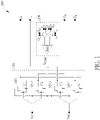
- FIG. 1 is a diagram illustrating a filter circuit with phase error calibration according to an embodiment of the present invention.
- the filter circuit 100 includes a polyphase filter 102 and a phase detector 104.
- the polyphase filter 102 is a circuit designed to generate a plurality of output signals I p , I n , Q p , Q n with different phases according to a plurality of input signals Vip and Vin. Ideally, when the input signals Vip and Vin form a differential input (i.e.
- the output signals I p , I n , Q p , Q n are quadrature signals, such that the output signals I p and Q p have a 90° phase difference therebetween, the output signals I n and Q n have a 90° phase difference therebetween, the output signals Q p and I n have a 90° phase difference therebetween, and the output signals Q n and I p have a 90° phase difference therebetween.
- the polyphase filter 102 is an active polyphase filter including a plurality of capacitors C1, C2, C3, C4 and a plurality of switch circuits implemented by metal-oxide-semiconductor (MOS) transistors such as N-channel metal-oxide-semiconductor (NMOS) transistors MN1, MN2, MN3, MN4.
- MOS metal-oxide-semiconductor
- NMOS N-channel metal-oxide-semiconductor
- Each of the NMOS transistors MN1-MN4 is used to act as a resistor when being turned on by a control voltage at a control terminal (i.e. a gate voltage at a gate terminal) . Since the active polyphase filter architecture is known to those skilled in the pertinent art, further description is omitted here for brevity.
- the filter circuit 100 includes the phase detector 104 that is a circuit designed to generate a tuning voltage Vtune in response to a phase error of the output signals I p , I n , Q p , Q n , wherein the same tuning voltage Vtune is supplied to gate terminals of the NMOS transistors MN1-MN4 for tuning the gate voltages of the NMOS transistors MN1-MN4. Since an on-resistance R on of an NMOS transistor depends on a gate-source voltage of the NMOS transistor, tuning the control voltages (i.e.
- the gate voltages of the NMOS transistors MN1-MN4 can achieve the objective of adjusting the on-resistance R on of each of the NMOS transistors MN1-MN4. In this way, the phase error of the output signals I p , I n , Q p , Q n can be reduced or cancelled by properly controlling the tuning voltage Vtune.
- the tuning voltage Vtune applied to the gate terminals of the NMOS transistors MN1-MN4 prevents any of the input signals Vip and Vin from having a rail-to-rail dynamic range, which degrades the jitter performance of the polyphase filter 102.
- the NMOS switch needs to be turned on for providing an on-resistance when the input signal Vip (or Vin) has a logic high level.
- the highest voltage of the input signal Vip (or Vin) fails to reach the supply voltage VDD.
- the present invention proposes a polyphase filter with dynamic range enhancement.
- FIG. 2 is a diagram illustrating a polyphase filter with dynamic range enhancement according to an embodiment of the present invention.
- FIG. 3 is a diagram illustrating a filter circuit using the polyphase filter shown in FIG. 2 according to an embodiment of the present invention.
- the filter circuit 100 shown in FIG. 1 may be modified to have the polyphase filter 102 replaced with the polyphase filter 200 to benefit from a dynamic range enhancement technique employed by the polyphase filter 200.
- the filter circuit 300 includes the proposed polyphase filter 200 shown in FIG. 2 and the phase detector 104 shown in FIG. 1 .
- polyphase filters 102 and 200 The major difference between the polyphase filters 102 and 200 is that additional circuit elements, including feed-forward capacitors C_ff1, C_ff2, C_ff3, C_ff4 and resistors R1, R2, R3, R4, are employed by the polyphase filter 200.
- additional circuit elements including feed-forward capacitors C_ff1, C_ff2, C_ff3, C_ff4 and resistors R1, R2, R3, R4, are employed by the polyphase filter 200.
- the proposed polyphase filter 200 is an active polyphase filter having switch circuits implemented by MOS transistors such as NMOS transistors MN1, MN2, MN3, MN4, where each of the NMOS transistors MN1-MN4 possesses an on-resistance R on when being turned on by a control voltage (gate voltage).
- MOS transistors such as NMOS transistors MN1, MN2, MN3, MN4, where each of the NMOS transistors MN1-MN4 possesses an on-resistance R on when being turned on by a control voltage (gate voltage).
- gate voltage gate voltage
- resistors needed by the polyphase filter 200 can be realized by the turned-on NMOS switches.
- the NMOS transistor MN1 it has a control terminal (i.e. gate terminal), a first connection terminal (i.e. drain terminal), and a second connection terminal (i.e. source terminal), wherein the first connection terminal (i.e.
- the feed-forward capacitor C_ff1 has a first plate N11 coupled to the second connection terminal (i.e. source terminal) of the NMOS transistor MN1, and has a second plate N12 coupled to the control terminal (i.e. gate terminal) of the NMOS transistor MN1.
- the resistor R1 is coupled between the tuning voltage Vtune and the control terminal (i.e. gate terminal) of the NMOS transistor MN1.
- the resistor R1 has one end for receiving the tuning voltage Vtune and the other end coupled to the control terminal (i.e. gate terminal) of the NMOS transistor MN1.
- the NMOS transistor MN2 has a control terminal (i.e. gate terminal), a first connection terminal (i.e. drain terminal), and a second connection terminal (i.e. source terminal), wherein the first connection terminal (i.e. drain terminal) is arranged to generate and output the output signal Q p , and the second connection terminal (i.e. source terminal) is arranged to receive the input signal Vip.
- the feed-forward capacitor C_ff2 has a first plate N21 coupled to the second connection terminal (i.e. source terminal) of the NMOS transistor MN2, and has a second plate N22 coupled to the control terminal (i.e. gate terminal) of the NMOS transistor MN2.
- the resistor R2 is coupled between the tuning voltage Vtune and the control terminal (i.e. gate terminal) of the NMOS transistor MN2. Specifically, the resistor R2 has one end for receiving the tuning voltage Vtune and the other end coupled to the control terminal (i.e. gate terminal) of the NMOS transistor MN2.
- the NMOS transistor MN3 has a control terminal (i.e. gate terminal), a first connection terminal (i.e. drain terminal), and a second connection terminal (i.e. source terminal), wherein the first connection terminal (i.e. drain terminal) is arranged to generate and output the output signal I n , and the second connection terminal (i.e. source terminal) is arranged to receive the input signal Vin.
- the feed-forward capacitor C_ff3 has a first plate N31 coupled to the second connection terminal (i.e. source terminal) of the NMOS transistor MN3, and has a second plate N32 coupled to the control terminal (i.e. gate terminal) of the NMOS transistor MN3.
- the resistor R3 is coupled between the tuning voltage and the control terminal (i.e. gate terminal) of the NMOS transistor MN3. Specifically, the resistor R3 has one end for receiving the tuning voltage Vtune and the other end coupled to the control terminal (i.e. gate terminal) of the NMOS transistor MN3.
- the NMOS transistor MN4 has a control terminal (i.e. gate terminal), a first connection terminal (i.e. drain terminal), and a second connection terminal (i.e. source terminal), wherein the first connection terminal (i.e. drain terminal) is arranged to generate and output the output signal Q n , and the second connection terminal (i.e. source terminal) is arranged to receive the input signal Vin.
- the feed-forward capacitor C_ff4 has a first plate N41 coupled to the second connection terminal (i.e. source terminal) of the NMOS transistor MN4, and has a second plate N42 coupled to the control terminal (i.e. gate terminal) of the NMOS transistor MN4.
- the resistor R4 is coupled between the tuning voltage and the control terminal (i.e. gate terminal) of the NMOS transistor MN4. Specifically, the resistor R4 has one end for receiving the tuning voltage Vtune and the other end coupled to the control terminal (i.e. gate terminal) of the NMOS transistor MN4.
- the input signals Vip and Vin form a differential input and therefore have a 180° phase difference therebetween, and/or the input signals Vip and Vin may be clock signals (e.g. local oscillator (LO) signals) generated from a clock generator.
- LO local oscillator
- the polyphase filter 200 may be used to generate the output signals I p , I n , Q p , Q n as LO signals with different phases.
- the input signals Vip and Vin may be a differential LO signal
- the output signal I p may serve as an LO signal with a 0° phase
- the output signal Q p may serve as an LO signal with a 90° phase
- the output signal I n may serve as an LO signal with a 180° phase
- the output signal Q n may serve as an LO signal with a 270° phase.
- a high-pass filter 202 is formed by the feed-forward capacitor C_ff1 and the resistor R1.
- the high-pass filter 202 has an input port (i.e. first plate N11 of feed-forward capacitor C1) coupled to the second connection terminal (i.e. source terminal) of the NMOS transistor MN1 and an output port (i.e. second plate N12 of feed-forward capacitor C1) coupled to the control terminal (i.e. gate terminal) of the NMOS transistor MN1, and is arranged to apply high-pass filtering to the input signal Vip for generating a filter output at the output port N12.
- the input signal Vip is a high-frequency signal such as an LO signal.
- the input signal Vip is passed to the output port N12 through the high-pass filter 202, and is involved in setting the control voltage at the control terminal (i.e. gate terminal) of the NMOS transistor MN1.
- a high-pass filter 204 is formed by the feed-forward capacitor C_ff2 and the resistor R2.
- the high-pass filter 204 has an input port (i.e. first plate N21 of feed-forward capacitor C2) coupled to the second connection terminal (i.e. source terminal) of the NMOS transistor MN2 and an output port (i.e. second plate N22 of feed-forward capacitor C2) coupled to the control terminal (i.e. gate terminal) of the NMOS transistor MN2, and is arranged to apply high-pass filtering to the input signal Vip for generating a filter output at the output port N22.
- the input signal Vip is a high-frequency signal such as an LO signal.
- the input signal Vip is passed to the output port N22 through the high-pass filter 204, and is involved in setting the control voltage at the control terminal (i.e. gate terminal) of the NMOS transistor MN2.
- a high-pass filter 206 is formed by the feed-forward capacitor C_ff3 and the resistor R3.
- the high-pass filter 206 has an input port (i.e. first plate N31 of feed-forward capacitor C3) coupled to the second connection terminal (i.e. source terminal) of the NMOS transistor MN3 and an output port (i.e. second plate N32 of feed-forward capacitor C3) coupled to the control terminal (i.e. gate terminal) of the NMOS transistor MN3, and is arranged to apply high-pass filtering to the input signal Vin for generating a filter output at the output port N32.
- the input signal Vin is a high-frequency signal such as an LO signal.
- the input signal Vin is passed to the output port N32 through the high-pass filter 206, and is involved in setting the control voltage at the control terminal (i.e. gate terminal) of the NMOS transistor MN3.
- a high-pass filter 208 is formed by the feed-forward capacitor C_ff4 and the resistor R4.
- the high-pass filter 208 has an input port (i.e. first plate N41 of feed-forward capacitor C4) coupled to the second connection terminal (i.e. source terminal) of the NMOS transistor MN4 and an output port (i.e. second plate N42 of feed-forward capacitor C4) coupled to the control terminal (i.e. gate terminal) of the NMOS transistor MN4, and is arranged to apply high-pass filtering to the input signal Vin for generating a filter output at the output port N42.
- the input signal Vin is a high-frequency signal such as an LO signal.
- the input signal Vin is passed to the output port N42 through the high-pass filter 208, and is involved in setting the control voltage at the control terminal (i.e. gate terminal) of the NMOS transistor MN4.
- the NMOS transistors MN1-MN4 can be turned into continuous-time bootstrapped switch circuits. Specifically, the arrangement of the feed-forward capacitor C_ff1 bootstraps the gate voltage of the NMOS transistor MN1 to the source voltage of the NMOS transistor MN1, thus allowing the two voltages to change in unison. Since the tuning voltage Vtune is coupled to the control terminal (i.e. gate terminal) of the NMOS transistor MN1 via the resistor R1, the tuning voltage Vtune is also involved in setting the control voltage (gate voltage) of the NMOS transistor MN1.
- the arrangement of the feed-forward capacitor C_ff2 bootstraps the gate voltage of the NMOS transistor MN2 to the source voltage of the NMOS transistor MN2, thus allowing the two voltages to change in unison.
- the tuning voltage Vtune is coupled to the control terminal (i.e. gate terminal) of the NMOS transistor MN2 via the resistor R2, the tuning voltage Vtune is also involved in setting the control voltage (gate voltage) of the NMOS transistor MN2.
- the control voltage (gate voltage) of the NMOS transistor MN2 may be set by Vtune+Vip. Since the gate-source voltage V GS is fixed at Vtune (i.e.
- the arrangement of the feed-forward capacitor C_ff3 bootstraps the gate voltage of the NMOS transistor MN3 to the source voltage of the NMOS transistor MN3, thus allowing the two voltages to change in unison.
- the tuning voltage Vtune is coupled to the control terminal (i.e. gate terminal) of the NMOS transistor MN3 via the resistor R3, the tuning voltage Vtune is also involved in setting the control voltage (gate voltage) of the NMOS transistor MN3.
- the control voltage (gate voltage) of the NMOS transistor MN3 may be set by Vtune+Vin. Since the gate-source voltage V GS is fixed at Vtune (i.e.
- the arrangement of the feed-forward capacitor C_ff4 bootstraps the gate voltage of the NMOS transistor MN4 to the source voltage of the NMOS transistor MN4, thus allowing the two voltages to change in unison.
- the tuning voltage Vtune is coupled to the control terminal (i.e. gate terminal) of the NMOS transistor MN4 via the resistor R4, the tuning voltage Vtune is also involved in setting the control voltage (gate voltage) of the NMOS transistor MN4.
- the control voltage (gate voltage) of the NMOS transistor MN4 may be set by Vtune+Vin. Since the gate-source voltage V GS is fixed at Vtune (i.e.
- a filter circuit using the proposed polyphase filter with dynamic range enhancement may be employed by a clock generator such as a quadrature LO signal generator.
- a clock generator such as a quadrature LO signal generator.
- this is for illustrative purposes only, and is not meant to be a limitation of the present invention. In practice, any application that adopts a filter circuit using the proposed polyphase filter with dynamic range enhancement falls within the scope of the present invention.
- the present invention may also be defined by means of the following numbered clauses.
Landscapes
- Physics & Mathematics (AREA)
- Nonlinear Science (AREA)
- Networks Using Active Elements (AREA)
Abstract
Description
- This application claims the benefit of
U.S. provisional application No. 63/120,756, filed on 12/03/2020 - The present invention relates to a filter design, and more particularly, to a filter circuit using a polyphase filter with dynamic range enhancement.
- A conventional passive polyphase filter includes a circuit constructed in a ring shape using four resistors and four capacitors, wherein the resistors and the capacitors are alternately connected in series. In addition, the conventional passive polyphase filter includes first and second input terminals and first through fourth output terminals, wherein an input signal with a predetermined frequency is differentially received by the first input terminal and the second input terminal, and four output signals with the same predetermined frequency but different phases are outputted from the first through fourth output terminals, respectively. However, the resistors may have the same resistance value that is deviated from a nominal value due to certain factors, and/or the capacitors may have the same capacitance value that is deviated from a nominal value due to certain factors. As a result, the output signals of the conventional passive polyphase filter suffer from a phase error introduced by imperfection of resistors and/or capacitors. There is a need for an innovative polyphase filter design that is capable of calibrating the phase error with less impact on the filter performance.
- One of the objectives of the claimed invention is to provide a filter circuit using a polyphase filter with dynamic range enhancement. One of the benefits of using the proposed polyphase filter with dynamic range enhancement is that the phase error at the polyphase filter outputs can be calibrated without introducing degradation of the filter performance.
- According to a first aspect of the present invention, an exemplary filter circuit is disclosed. The exemplary filter circuit includes a polyphase filter arranged to generate a plurality of output signals with different phases according to a plurality of input signals. The polyphase filter includes a switch circuit and a feed-forward capacitor. The switch circuit has a control terminal arranged to receive a control voltage, a first connection terminal arranged to output one of the output signals, and a second connection terminal arranged to receive one of the input signals. The feed-forward capacitor has a first plate coupled to the second connection terminal of the switch circuit and a second plate coupled to the control terminal of the switch circuit.
- According to a second aspect of the present invention, an exemplary filter circuit is disclosed. The exemplary filter circuit includes a polyphase filter arranged to generate a plurality of output signals with different phases according to a plurality of input signals. The polyphase filter includes a continuous-time bootstrapped switch circuit, having a control terminal arranged to receive a control voltage, a first connection terminal arranged to output one of the output signals, and a second connection terminal arranged to receive one of the input signals.
- According to a third aspect of the present invention, an exemplary filter circuit is disclosed. The exemplary filter circuit includes a polyphase filter arranged to generate a plurality of output signals with different phases according to a plurality of input signals. The polyphase filter includes a switch circuit and a high-pass filter. The switch circuit has a control terminal arranged to receive a control voltage, a first connection terminal arranged to output one of the output signals, and a second connection terminal arranged to receive one of the input signals. The high-pass filter has an input port coupled to the second connection terminal of the switch circuit and an output port coupled to the control terminal of the switch circuit, and arranged to apply high-pass filtering to said one of the input signals for generating a filter output at the output port, wherein the filter output is involved in setting the control voltage.
- These and other objectives of the present invention will no doubt become obvious to those of ordinary skill in the art after reading the following detailed description of the preferred embodiment that is illustrated in the various figures and drawings.
-
-
FIG. 1 is a diagram illustrating a filter circuit with phase error calibration according to an embodiment of the present invention. -
FIG. 2 is a diagram illustrating a polyphase filter with dynamic range enhancement according to an embodiment of the present invention. -
FIG. 3 is a diagram illustrating a filter circuit using the polyphase filter shown inFIG. 2 according to an embodiment of the present invention. - Certain terms are used throughout the following description and claims, which refer to particular components. As one skilled in the art will appreciate, electronic equipment manufacturers may refer to a component by different names. This document does not intend to distinguish between components that differ in name but not in function. In the following description and in the claims, the terms "include" and "comprise" are used in an open-ended fashion, and thus should be interpreted to mean "include, but not limited to ...". Also, the term "couple" is intended to mean either an indirect or direct electrical connection. Accordingly, if one device is coupled to another device, that connection may be through a direct electrical connection, or through an indirect electrical connection via other devices and connections.
-
FIG. 1 is a diagram illustrating a filter circuit with phase error calibration according to an embodiment of the present invention. Thefilter circuit 100 includes apolyphase filter 102 and aphase detector 104. Thepolyphase filter 102 is a circuit designed to generate a plurality of output signals Ip, In, Qp, Qn with different phases according to a plurality of input signals Vip and Vin. Ideally, when the input signals Vip and Vin form a differential input (i.e. the input signals Vip and Vin have a 180° phase difference therebetween), the output signals Ip, In, Qp, Qn are quadrature signals, such that the output signals Ip and Qp have a 90° phase difference therebetween, the output signals In and Qn have a 90° phase difference therebetween, the output signals Qp and In have a 90° phase difference therebetween, and the output signals Qn and Ip have a 90° phase difference therebetween. - As shown in
FIG. 1 , thepolyphase filter 102 is an active polyphase filter including a plurality of capacitors C1, C2, C3, C4
and a plurality of switch circuits implemented by metal-oxide-semiconductor (MOS) transistors such as N-channel metal-oxide-semiconductor (NMOS) transistors MN1, MN2, MN3, MN4. Each of the NMOS transistors MN1-MN4 is used to act as a resistor when being turned on by a control voltage at a control terminal (i.e. a gate voltage at a gate terminal) . Since the active polyphase filter architecture is known to those skilled in the pertinent art, further description is omitted here for brevity. - To address the phase error issue encountered by the
polyphase filter 102, thefilter circuit 100 includes thephase detector 104 that is a circuit designed to generate a tuning voltage Vtune in response to a phase error of the output signals Ip, In, Qp, Qn, wherein the same tuning voltage Vtune is supplied to gate terminals of the NMOS transistors MN1-MN4 for tuning the gate voltages of the NMOS transistors MN1-MN4. Since an on-resistance Ron of an NMOS transistor depends on a gate-source voltage of the NMOS transistor, tuning the control voltages (i.e. gate voltages) of the NMOS transistors MN1-MN4 can achieve the objective of adjusting the on-resistance Ron of each of the NMOS transistors MN1-MN4. In this way, the phase error of the output signals Ip, In, Qp, Qn can be reduced or cancelled by properly controlling the tuning voltage Vtune. - However, the tuning voltage Vtune applied to the gate terminals of the NMOS transistors MN1-MN4 prevents any of the input signals Vip and Vin from having a rail-to-rail dynamic range, which degrades the jitter performance of the
polyphase filter 102. For example, the NMOS switch needs to be turned on for providing an on-resistance when the input signal Vip (or Vin) has a logic high level. Hence, the highest voltage of the input signal Vip (or Vin) fails to reach the supply voltage VDD. To address this issue, the present invention proposes a polyphase filter with dynamic range enhancement. - Please refer to
FIG. 2 in conjunction withFIG. 3 .FIG. 2 is a diagram illustrating a polyphase filter with dynamic range enhancement according to an embodiment of the present invention.FIG. 3 is a diagram illustrating a filter circuit using the polyphase filter shown inFIG. 2 according to an embodiment of the present invention. Thefilter circuit 100 shown inFIG. 1 may be modified to have thepolyphase filter 102 replaced with thepolyphase filter 200 to benefit from a dynamic range enhancement technique employed by thepolyphase filter 200. Taking the embodiment shown inFIG. 3 for example, thefilter circuit 300 includes the proposedpolyphase filter 200 shown inFIG. 2 and thephase detector 104 shown inFIG. 1 . The major difference between thepolyphase filters polyphase filter 200. - The proposed
polyphase filter 200 is an active polyphase filter having switch circuits implemented by MOS transistors such as NMOS transistors MN1, MN2, MN3, MN4, where each of the NMOS transistors MN1-MN4 possesses an on-resistance Ron when being turned on by a control voltage (gate voltage). In other words, resistors needed by thepolyphase filter 200 can be realized by the turned-on NMOS switches. Regarding the NMOS transistor MN1, it has a control terminal (i.e. gate terminal), a first connection terminal (i.e. drain terminal), and a second connection terminal (i.e. source terminal), wherein the first connection terminal (i.e. drain terminal) is arranged to generate and output the output signal Ip, and the second connection terminal (i.e. source terminal) is arranged to receive the input signal Vip. The feed-forward capacitor C_ff1 has a first plate N11 coupled to the second connection terminal (i.e. source terminal) of the NMOS transistor MN1, and has a second plate N12 coupled to the control terminal (i.e. gate terminal) of the NMOS transistor MN1. In addition, the resistor R1 is coupled between the tuning voltage Vtune and the control terminal (i.e. gate terminal) of the NMOS transistor MN1. Specifically, the resistor R1 has one end for receiving the tuning voltage Vtune and the other end coupled to the control terminal (i.e. gate terminal) of the NMOS transistor MN1. - Regarding the NMOS transistor MN2, it has a control terminal (i.e. gate terminal), a first connection terminal (i.e. drain terminal), and a second connection terminal (i.e. source terminal), wherein the first connection terminal (i.e. drain terminal) is arranged to generate and output the output signal Qp, and the second connection terminal (i.e. source terminal) is arranged to receive the input signal Vip. The feed-forward capacitor C_ff2 has a first plate N21 coupled to the second connection terminal (i.e. source terminal) of the NMOS transistor MN2, and has a second plate N22 coupled to the control terminal (i.e. gate terminal) of the NMOS transistor MN2. In addition, the resistor R2 is coupled between the tuning voltage Vtune and the control terminal (i.e. gate terminal) of the NMOS transistor MN2. Specifically, the resistor R2 has one end for receiving the tuning voltage Vtune and the other end coupled to the control terminal (i.e. gate terminal) of the NMOS transistor MN2.
- Regarding the NMOS transistor MN3, it has a control terminal (i.e. gate terminal), a first connection terminal (i.e. drain terminal), and a second connection terminal (i.e. source terminal), wherein the first connection terminal (i.e. drain terminal) is arranged to generate and output the output signal In, and the second connection terminal (i.e. source terminal) is arranged to receive the input signal Vin. The feed-forward capacitor C_ff3 has a first plate N31 coupled to the second connection terminal (i.e. source terminal) of the NMOS transistor MN3, and has a second plate N32 coupled to the control terminal (i.e. gate terminal) of the NMOS transistor MN3. In addition, the resistor R3 is coupled between the tuning voltage and the control terminal (i.e. gate terminal) of the NMOS transistor MN3. Specifically, the resistor R3 has one end for receiving the tuning voltage Vtune and the other end coupled to the control terminal (i.e. gate terminal) of the NMOS transistor MN3.
- Regarding the NMOS transistor MN4, it has a control terminal (i.e. gate terminal), a first connection terminal (i.e. drain terminal), and a second connection terminal (i.e. source terminal), wherein the first connection terminal (i.e. drain terminal) is arranged to generate and output the output signal Qn, and the second connection terminal (i.e. source terminal) is arranged to receive the input signal Vin. The feed-forward capacitor C_ff4 has a first plate N41 coupled to the second connection terminal (i.e. source terminal) of the NMOS transistor MN4, and has a second plate N42 coupled to the control terminal (i.e. gate terminal) of the NMOS transistor MN4. In addition, the resistor R4 is coupled between the tuning voltage and the control terminal (i.e. gate terminal) of the NMOS transistor MN4. Specifically, the resistor R4 has one end for receiving the tuning voltage Vtune and the other end coupled to the control terminal (i.e. gate terminal) of the NMOS transistor MN4.
- In this embodiment, all of the feed-forward capacitors C_ff1-C_ff4 may have the same capacitance value CHPF, that is, C_eff1=C_eff2=C_eff3=C_eff1=CHPF, and all of the resistors R1-R4 may have the same resistance value RHPF, that is, R1=R2=R3=R4=RHPF. In some embodiments of the present invention, the input signals Vip and Vin form a differential input and therefore have a 180° phase difference therebetween, and/or the input signals Vip and Vin may be clock signals (e.g. local oscillator (LO) signals) generated from a clock generator. Hence, in a wireless communication application, the
polyphase filter 200 may be used to generate the output signals Ip, In, Qp, Qn as LO signals with different phases. For example, the input signals Vip and Vin may be a differential LO signal, the output signal Ip may serve as an LO signal with a 0° phase, the output signal Qp may serve as an LO signal with a 90° phase, the output signal In may serve as an LO signal with a 180° phase, and the output signal Qn may serve as an LO signal with a 270° phase. - A high-
pass filter 202 is formed by the feed-forward capacitor C_ff1 and the resistor R1. The high-pass filter 202 has an input port (i.e. first plate N11 of feed-forward capacitor C1) coupled to the second connection terminal (i.e. source terminal) of the NMOS transistor MN1 and an output port (i.e. second plate N12 of feed-forward capacitor C1) coupled to the control terminal (i.e. gate terminal) of the NMOS transistor MN1, and is arranged to apply high-pass filtering to the input signal Vip for generating a filter output at the output port N12. In this embodiment, the input signal Vip is a high-frequency signal such as an LO signal. Hence, the input signal Vip is passed to the output port N12 through the high-pass filter 202, and is involved in setting the control voltage at the control terminal (i.e. gate terminal) of the NMOS transistor MN1. - Similarly, a high-
pass filter 204 is formed by the feed-forward capacitor C_ff2 and the resistor R2. The high-pass filter 204 has an input port (i.e. first plate N21 of feed-forward capacitor C2) coupled to the second connection terminal (i.e. source terminal) of the NMOS transistor MN2 and an output port (i.e. second plate N22 of feed-forward capacitor C2) coupled to the control terminal (i.e. gate terminal) of the NMOS transistor MN2, and is arranged to apply high-pass filtering to the input signal Vip for generating a filter output at the output port N22. In this embodiment, the input signal Vip is a high-frequency signal such as an LO signal. Hence, the input signal Vip is passed to the output port N22 through the high-pass filter 204, and is involved in setting the control voltage at the control terminal (i.e. gate terminal) of the NMOS transistor MN2. - A high-
pass filter 206 is formed by the feed-forward capacitor C_ff3 and the resistor R3. The high-pass filter 206 has an input port (i.e. first plate N31 of feed-forward capacitor C3) coupled to the second connection terminal (i.e. source terminal) of the NMOS transistor MN3 and an output port (i.e. second plate N32 of feed-forward capacitor C3) coupled to the control terminal (i.e. gate terminal) of the NMOS transistor MN3, and is arranged to apply high-pass filtering to the input signal Vin for generating a filter output at the output port N32. In this embodiment, the input signal Vin is a high-frequency signal such as an LO signal. Hence, the input signal Vin is passed to the output port N32 through the high-pass filter 206, and is involved in setting the control voltage at the control terminal (i.e. gate terminal) of the NMOS transistor MN3. - A high-pass filter 208 is formed by the feed-forward capacitor C_ff4 and the resistor R4. The high-pass filter 208 has an input port (i.e. first plate N41 of feed-forward capacitor C4) coupled to the second connection terminal (i.e. source terminal) of the NMOS transistor MN4 and an output port (i.e. second plate N42 of feed-forward capacitor C4) coupled to the control terminal (i.e. gate terminal) of the NMOS transistor MN4, and is arranged to apply high-pass filtering to the input signal Vin for generating a filter output at the output port N42. In this embodiment, the input signal Vin is a high-frequency signal such as an LO signal. Hence, the input signal Vin is passed to the output port N42 through the high-pass filter 208, and is involved in setting the control voltage at the control terminal (i.e. gate terminal) of the NMOS transistor MN4.
- With the use of feed-forward capacitors C_ff1-C_ff4, the NMOS transistors MN1-MN4 can be turned into continuous-time bootstrapped switch circuits. Specifically, the arrangement of the feed-forward capacitor C_ff1 bootstraps the gate voltage of the NMOS transistor MN1 to the source voltage of the NMOS transistor MN1, thus allowing the two voltages to change in unison. Since the tuning voltage Vtune is coupled to the control terminal (i.e. gate terminal) of the NMOS transistor MN1 via the resistor R1, the tuning voltage Vtune is also involved in setting the control voltage (gate voltage) of the NMOS transistor MN1. For example, the control voltage (gate voltage) of the NMOS transistor MN1 may be set by Vtune+Vip. Since the gate-source voltage VGS is fixed at Vtune (i.e. VGS=Vtune+Vip-Vip=Vtune) regardless of the voltage level of the input signal Vip, the on-resistance Ron of the NMOS transistor MN1 is kept constant, and the input signal Vip received by the NMOS transistor MN1 is allowed to have a rail-to-rail dynamic range.
- Similarly, the arrangement of the feed-forward capacitor C_ff2 bootstraps the gate voltage of the NMOS transistor MN2 to the source voltage of the NMOS transistor MN2, thus allowing the two voltages to change in unison. Since the tuning voltage Vtune is coupled to the control terminal (i.e. gate terminal) of the NMOS transistor MN2 via the resistor R2, the tuning voltage Vtune is also involved in setting the control voltage (gate voltage) of the NMOS transistor MN2. For example, the control voltage (gate voltage) of the NMOS transistor MN2 may be set by Vtune+Vip. Since the gate-source voltage VGS is fixed at Vtune (i.e. VGS=Vtune+Vip-Vip=Vtune) regardless of the voltage level of the input signal Vip, the on-resistance Ron of the NMOS transistor MN2 is kept constant, and the input signal Vip received by the NMOS transistor MN2 is allowed to have a rail-to-rail dynamic range.
- The arrangement of the feed-forward capacitor C_ff3 bootstraps the gate voltage of the NMOS transistor MN3 to the source voltage of the NMOS transistor MN3, thus allowing the two voltages to change in unison. Since the tuning voltage Vtune is coupled to the control terminal (i.e. gate terminal) of the NMOS transistor MN3 via the resistor R3, the tuning voltage Vtune is also involved in setting the control voltage (gate voltage) of the NMOS transistor MN3. For example, the control voltage (gate voltage) of the NMOS transistor MN3 may be set by Vtune+Vin. Since the gate-source voltage VGS is fixed at Vtune (i.e. VGS=Vtune+Vin-Vin=Vtune) regardless of the voltage level of the input signal Vin, the on-resistance Ron of the NMOS transistor MN3 is kept constant, and the input signal Vin received by the NMOS transistor MN3 is allowed to have a rail-to-rail dynamic range.
- The arrangement of the feed-forward capacitor C_ff4 bootstraps the gate voltage of the NMOS transistor MN4 to the source voltage of the NMOS transistor MN4, thus allowing the two voltages to change in unison. Since the tuning voltage Vtune is coupled to the control terminal (i.e. gate terminal) of the NMOS transistor MN4 via the resistor R4, the tuning voltage Vtune is also involved in setting the control voltage (gate voltage) of the NMOS transistor MN4. For example, the control voltage (gate voltage) of the NMOS transistor MN4 may be set by Vtune+Vin. Since the gate-source voltage VGS is fixed at Vtune (i.e. VGS=Vtune+Vin-Vin=Vtune) regardless of the voltage level of the input signal Vin, the on-resistance Ron of the NMOS transistor MN4 is kept constant, and the input signal Vin received by the NMOS transistor MN4 is allowed to have a rail-to-rail dynamic range.
- In the above embodiment, a filter circuit using the proposed polyphase filter with dynamic range enhancement may be employed by a clock generator such as a quadrature LO signal generator. However, this is for illustrative purposes only, and is not meant to be a limitation of the present invention. In practice, any application that adopts a filter circuit using the proposed polyphase filter with dynamic range enhancement falls within the scope of the present invention.
- Those skilled in the art will readily observe that numerous modifications and alterations of the device and method may be made while retaining the teachings of the invention. Accordingly, the above disclosure should be construed as limited only by the metes and bounds of the appended claims.
- The present invention may also be defined by means of the following numbered clauses.
- 1. A filter circuit comprising:
- a polyphase filter, arranged to generate a plurality of output signals with different phases according to a plurality of input signals,
- wherein the polyphase filter comprises:
- a switch circuit, having a control terminal arranged to receive a control voltage, a first connection terminal arranged to output one of the plurality of output signals, and a second connection terminal arranged to receive one of the plurality of input signals; and
- a feed-forward capacitor, having a first plate coupled to the second connection terminal of the switch circuit and a second plate coupled to the control terminal of the switch circuit.
- 2. The filter circuit of clause 1, further comprising:
- a phase detector, arranged to generate a tuning voltage in response to a phase error of the plurality of output signals;
- wherein the polyphase filter further comprises:
a resistor, having a first end arranged to receive the tuning voltage and a second end coupled to the control terminal of the switch circuit, wherein the tuning voltage is involved in setting the control voltage.
- 3. The filter circuit of clause 1, wherein the plurality of input signals comprise a differential input.
- 4. The filter circuit of clause 1, wherein the plurality of input signals comprise clock signals.
- 5. The filter circuit of clause 1, wherein the switch circuit is a metal-oxide-semiconductor (MOS) transistor.
- 6. The filter circuit of clause 5, wherein the MOS transistor has a fixed on-resistance, regardless of a voltage level of said one of the plurality of input signals.
- 7. A filter circuit comprising:
- a polyphase filter, arranged to generate a plurality of output signals with different phases according to a plurality of input signals,
- wherein the polyphase filter comprises:
a continuous-time bootstrapped switch circuit, having a control terminal arranged to receive a control voltage, a first connection terminal arranged to output one of the plurality of output signals, and a second connection terminal arranged to receive one of the plurality of input signals.
- 8. The filter circuit of clause 7, further comprising:
- a phase detector, arranged to generate a tuning voltage in response to a phase error of the plurality of output signals;
- wherein the polyphase filter further comprises:
a resistor, having a first end arranged to receive the tuning voltage and a second end coupled to the control terminal of the continuous-time bootstrapped switch.
- 9. The filter circuit of clause 7, wherein the plurality of input signals comprise a differential input.
- 10. The filter circuit of clause 7, wherein the plurality of input signals comprise clock signals.
- 11. A filter circuit comprising:
- a polyphase filter, arranged to generate a plurality of output signals with different phases according to a plurality of input signals,
- wherein the polyphase filter comprises:
- a switch circuit, having a control terminal arranged to receive a control voltage, a first connection terminal arranged to output one of the plurality of output signals, and a second connection terminal arranged to receive one of the plurality of input signals; and
- a high-pass filter, having an input port coupled to the second connection terminal of the switch circuit and an output port coupled to the control terminal of the switch circuit, and arranged to apply high-pass filtering to said one of the plurality of input signals for generating a filter output at the output port, wherein the filter output is involved in setting the control voltage.
- 12. The filter circuit of clause 11, further comprising:
- a phase detector, arranged to generate a tuning voltage in response to a phase error of the plurality of output signals;
- wherein the tuning voltage is also involved in setting the control voltage.
- 13. The filter circuit of clause 11, wherein the plurality of input signals comprise a differential input.
- 14. The filter circuit of clause 11, wherein the plurality of input signals comprise clock signals.
- 15. The filter circuit of clause 11, wherein the switch circuit is a metal-oxide-semiconductor (MOS) transistor.
- 16. The filter circuit of clause 15, wherein the MOS transistor has a fixed on-resistance, regardless of a voltage level of said one of the plurality of input signals.
Claims (15)
- A filter circuit (100) comprising:
a polyphase filter (102, 200), arranged to generate a plurality of output signals with different phases according to a plurality of input signals, wherein the polyphase filter (102, 200) comprises:a switch circuit, having a control terminal arranged to receive a control voltage, a first connection terminal arranged to output one of the plurality of output signals, and a second connection terminal arranged to receive one of the plurality of input signals; anda feed-forward capacitor (C_ff1, C_ff2, C_ff3, C_ff4), having a first plate coupled to the second connection terminal of the switch circuit and a second plate coupled to the control terminal of the switch circuit. - The filter circuit (100) of claim 1, further comprising:a phase detector, arranged to generate a tuning voltage in response to a phase error of the plurality of output signals;wherein the polyphase filter (102, 200) further comprises:
a resistor (R1, R2, R3, R4), having a first end arranged to receive the tuning voltage and a second end coupled to the control terminal of the switch circuit, wherein the tuning voltage is involved in setting the control voltage. - The filter circuit (100) of claim 1, wherein the plurality of input signals comprise a differential input.
- The filter circuit (100) of claim 1, wherein the plurality of input signals comprise clock signals.
- The filter circuit (100) of claim 1, wherein the switch circuit is a metal-oxide-semiconductor, MOS, transistor.
- The filter circuit (100) of claim 5, wherein the MOS transistor has a fixed on-resistance, regardless of a voltage level of said one of the plurality of input signals.
- A filter circuit (100) comprising:
a polyphase filter (102, 200), arranged to generate a plurality of output signals with different phases according to a plurality of input signals, wherein the polyphase filter (102, 200) comprises:
a continuous-time bootstrapped switch circuit, having a control terminal arranged to receive a control voltage, a first connection terminal arranged to output one of the plurality of output signals, and a second connection terminal arranged to receive one of the plurality of input signals. - The filter circuit (100) of claim 7, further comprising:a phase detector, arranged to generate a tuning voltage in response to a phase error of the plurality of output signals;wherein the polyphase filter (102, 200) further comprises:
a resistor (R1, R2, R3, R4), having a first end arranged to receive the tuning voltage and a second end coupled to the control terminal of the continuous-time bootstrapped switch. - The filter circuit (100) of claim 7, wherein the plurality of input signals comprise a differential input; or
wherein the plurality of input signals comprise clock signals. - A filter circuit (100) comprising:
a polyphase filter (102, 200), arranged to generate a plurality of output signals with different phases according to a plurality of input signals, wherein the polyphase filter (102, 200) comprises:a switch circuit, having a control terminal arranged to receive a control voltage, a first connection terminal arranged to output one of the plurality of output signals, and a second connection terminal arranged to receive one of the plurality of input signals; anda high-pass filter (202, 204, 206, 208), having an input port coupled to the second connection terminal of the switch circuit and an output port coupled to the control terminal of the switch circuit, and arranged to apply high-pass filtering to said one of the plurality of input signals for generating a filter output at the output port, wherein the filter output is involved in setting the control voltage. - The filter circuit (100) of claim 10, further comprising:a phase detector (104), arranged to generate a tuning voltage in response to a phase error of the plurality of output signals;wherein the tuning voltage is also involved in setting the control voltage.
- The filter circuit (100) of claim 10, wherein the plurality of input signals comprise a differential input.
- The filter circuit (100) of claim 10, wherein the plurality of input signals comprise clock signals.
- The filter circuit of claim 10, wherein the switch circuit is a metal-oxide-semiconductor, MOS, transistor.
- The filter circuit (100) of claim 14, wherein the MOS transistor has a fixed on-resistance, regardless of a voltage level of said one of the plurality of input signals.
Applications Claiming Priority (2)
| Application Number | Priority Date | Filing Date | Title |
|---|---|---|---|
| US202063120756P | 2020-12-03 | 2020-12-03 | |
| US17/503,385 US20220182040A1 (en) | 2020-12-03 | 2021-10-18 | Filter circuit using polyphase filter with dynamic range enhancement |
Publications (1)
| Publication Number | Publication Date |
|---|---|
| EP4009521A1 true EP4009521A1 (en) | 2022-06-08 |
Family
ID=78617226
Family Applications (1)
| Application Number | Title | Priority Date | Filing Date |
|---|---|---|---|
| EP21207863.8A Withdrawn EP4009521A1 (en) | 2020-12-03 | 2021-11-11 | Filter circuit using polyphase filter with dynamic range enhancement |
Country Status (4)
| Country | Link |
|---|---|
| US (1) | US20220182040A1 (en) |
| EP (1) | EP4009521A1 (en) |
| CN (1) | CN114598297A (en) |
| TW (1) | TWI792709B (en) |
Citations (6)
| Publication number | Priority date | Publication date | Assignee | Title |
|---|---|---|---|---|
| JPS58103219A (en) * | 1981-12-15 | 1983-06-20 | Toshiba Corp | Variable linear resistance |
| US5563545A (en) * | 1992-03-03 | 1996-10-08 | Anadigics, Inc. | Low cost monolithic GaAs upconverter chip |
| US20060055442A1 (en) * | 2004-09-16 | 2006-03-16 | Matsushita Electric Industrial Co., Ltd. | Phase shifting device |
| US20140086364A1 (en) * | 2012-09-27 | 2014-03-27 | Analog Devices, Inc. | Apparatus and methods for quadrature clock signal generation |
| CN104300931A (en) * | 2013-07-16 | 2015-01-21 | 陕西北斗恒通信息科技有限公司 | Bandwidth-adjustable passive multiphase filter circuit |
| US20160065179A1 (en) * | 2014-08-28 | 2016-03-03 | Qualcomm Incorporated | High accuracy millimeter wave/radio frequency wideband in-phase and quadrature generation |
Family Cites Families (5)
| Publication number | Priority date | Publication date | Assignee | Title |
|---|---|---|---|---|
| US20040196089A1 (en) * | 2003-04-02 | 2004-10-07 | O'donnell John J. | Switching device |
| US7728650B2 (en) * | 2007-06-15 | 2010-06-01 | Qualcomm Incorporated | Switches with passive bootstrap of control signal |
| US8008988B1 (en) * | 2008-02-20 | 2011-08-30 | Triquint Semiconductor, Inc. | Radio frequency switch with improved intermodulation distortion through use of feed forward capacitor |
| US9106202B2 (en) * | 2013-04-17 | 2015-08-11 | Linear Technology Corporation | Poly-phase filter with phase tuning |
| CN108702140B (en) * | 2016-02-17 | 2021-07-16 | 三菱电机株式会社 | Polyphase Filters and Filter Circuits |
-
2021
- 2021-10-18 US US17/503,385 patent/US20220182040A1/en not_active Abandoned
- 2021-11-11 EP EP21207863.8A patent/EP4009521A1/en not_active Withdrawn
- 2021-11-24 TW TW110143734A patent/TWI792709B/en active
- 2021-11-26 CN CN202111423817.6A patent/CN114598297A/en not_active Withdrawn
Patent Citations (6)
| Publication number | Priority date | Publication date | Assignee | Title |
|---|---|---|---|---|
| JPS58103219A (en) * | 1981-12-15 | 1983-06-20 | Toshiba Corp | Variable linear resistance |
| US5563545A (en) * | 1992-03-03 | 1996-10-08 | Anadigics, Inc. | Low cost monolithic GaAs upconverter chip |
| US20060055442A1 (en) * | 2004-09-16 | 2006-03-16 | Matsushita Electric Industrial Co., Ltd. | Phase shifting device |
| US20140086364A1 (en) * | 2012-09-27 | 2014-03-27 | Analog Devices, Inc. | Apparatus and methods for quadrature clock signal generation |
| CN104300931A (en) * | 2013-07-16 | 2015-01-21 | 陕西北斗恒通信息科技有限公司 | Bandwidth-adjustable passive multiphase filter circuit |
| US20160065179A1 (en) * | 2014-08-28 | 2016-03-03 | Qualcomm Incorporated | High accuracy millimeter wave/radio frequency wideband in-phase and quadrature generation |
Non-Patent Citations (1)
| Title |
|---|
| SUNG HO WANG ET AL: "A 5-GHz band I/Q clock generator using a self-calibration technique", EURPOEAN SOLID-STATE CIRCUITS CONFERENCE, September 2002 (2002-09-01), pages 807 - 810, XP031919660 * |
Also Published As
| Publication number | Publication date |
|---|---|
| TWI792709B (en) | 2023-02-11 |
| US20220182040A1 (en) | 2022-06-09 |
| TW202224345A (en) | 2022-06-16 |
| CN114598297A (en) | 2022-06-07 |
Similar Documents
| Publication | Publication Date | Title |
|---|---|---|
| KR100299740B1 (en) | Filter circuit | |
| US6710644B2 (en) | Low pass filter corner frequency tuning circuit and method | |
| US20080272851A1 (en) | LC voltage controlled oscillator with tunable capacitance unit | |
| US7830285B2 (en) | Circuit with calibration circuit portion | |
| US11276912B2 (en) | Magnetic balun/transformer with post processing adjustments | |
| CN110784177B (en) | Voltage controlled oscillator, PLL circuit and CDR device | |
| US6882216B2 (en) | On-chip high-pass filter with large time constant | |
| US7755398B2 (en) | Time constant calibration device and related method thereof | |
| EP3182583A2 (en) | Oscillator scheme capable of reducing far-out phase noise and closed-in phase noise | |
| US9634561B1 (en) | Programmable charge pump | |
| Ler et al. | Compact, High-$ Q $, and Low-Current Dissipation CMOS Differential Active Inductor | |
| WO2006035372A1 (en) | Frequency-tunable oscillator arrangement | |
| US20220182040A1 (en) | Filter circuit using polyphase filter with dynamic range enhancement | |
| CN110858750B (en) | Charge pump circuit and related method | |
| KR19980086435A (en) | Correction circuit and electronic circuit device having the same | |
| CN115833787B (en) | CMOS active polyphase filter with adjustable suppression frequency | |
| WO2005117260A1 (en) | High voltage switch using low voltage cmos transistors | |
| EP1629594A1 (en) | Improvements in or relating to transconductor circuits | |
| US9255963B2 (en) | Built-in self-test circuit for voltage controlled oscillator | |
| US20070096799A1 (en) | Complex band-pass filter | |
| US7777579B2 (en) | Local oscillation generator with mixer having reduced signal power consumption | |
| US7164311B2 (en) | Method and apparatus for tuning GMC filter | |
| KR100274154B1 (en) | High low-noise ring oscillator delay cell | |
| US12088299B2 (en) | Clock distribution with transimpedance amplifier and biquad filter | |
| TWI831581B (en) | Transconductance amplifier of high linearity and common-mode rejection |
Legal Events
| Date | Code | Title | Description |
|---|---|---|---|
| PUAI | Public reference made under article 153(3) epc to a published international application that has entered the european phase |
Free format text: ORIGINAL CODE: 0009012 |
|
| STAA | Information on the status of an ep patent application or granted ep patent |
Free format text: STATUS: THE APPLICATION HAS BEEN PUBLISHED |
|
| AK | Designated contracting states |
Kind code of ref document: A1 Designated state(s): AL AT BE BG CH CY CZ DE DK EE ES FI FR GB GR HR HU IE IS IT LI LT LU LV MC MK MT NL NO PL PT RO RS SE SI SK SM TR |
|
| STAA | Information on the status of an ep patent application or granted ep patent |
Free format text: STATUS: REQUEST FOR EXAMINATION WAS MADE |
|
| 17P | Request for examination filed |
Effective date: 20221207 |
|
| RBV | Designated contracting states (corrected) |
Designated state(s): AL AT BE BG CH CY CZ DE DK EE ES FI FR GB GR HR HU IE IS IT LI LT LU LV MC MK MT NL NO PL PT RO RS SE SI SK SM TR |
|
| P01 | Opt-out of the competence of the unified patent court (upc) registered |
Effective date: 20230607 |
|
| STAA | Information on the status of an ep patent application or granted ep patent |
Free format text: STATUS: EXAMINATION IS IN PROGRESS |
|
| 17Q | First examination report despatched |
Effective date: 20250410 |
|
| STAA | Information on the status of an ep patent application or granted ep patent |
Free format text: STATUS: THE APPLICATION HAS BEEN WITHDRAWN |
|
| 18W | Application withdrawn |
Effective date: 20250523 |