EP4009340A1 - Capacitor structure with via embedded in porous medium - Google Patents
Capacitor structure with via embedded in porous medium Download PDFInfo
- Publication number
- EP4009340A1 EP4009340A1 EP20306479.5A EP20306479A EP4009340A1 EP 4009340 A1 EP4009340 A1 EP 4009340A1 EP 20306479 A EP20306479 A EP 20306479A EP 4009340 A1 EP4009340 A1 EP 4009340A1
- Authority
- EP
- European Patent Office
- Prior art keywords
- layer
- region
- pores
- conductive
- porous
- Prior art date
- Legal status (The legal status is an assumption and is not a legal conclusion. Google has not performed a legal analysis and makes no representation as to the accuracy of the status listed.)
- Granted
Links
Images







Classifications
-
- H—ELECTRICITY
- H01—ELECTRIC ELEMENTS
- H01G—CAPACITORS; CAPACITORS, RECTIFIERS, DETECTORS, SWITCHING DEVICES, LIGHT-SENSITIVE OR TEMPERATURE-SENSITIVE DEVICES OF THE ELECTROLYTIC TYPE
- H01G4/00—Fixed capacitors; Processes of their manufacture
- H01G4/002—Details
- H01G4/228—Terminals
-
- H—ELECTRICITY
- H10—SEMICONDUCTOR DEVICES; ELECTRIC SOLID-STATE DEVICES NOT OTHERWISE PROVIDED FOR
- H10D—INORGANIC ELECTRIC SEMICONDUCTOR DEVICES
- H10D1/00—Resistors, capacitors or inductors
- H10D1/01—Manufacture or treatment
- H10D1/041—Manufacture or treatment of capacitors having no potential barriers
- H10D1/043—Manufacture or treatment of capacitors having no potential barriers using patterning processes to form electrode extensions, e.g. etching
-
- H—ELECTRICITY
- H01—ELECTRIC ELEMENTS
- H01G—CAPACITORS; CAPACITORS, RECTIFIERS, DETECTORS, SWITCHING DEVICES, LIGHT-SENSITIVE OR TEMPERATURE-SENSITIVE DEVICES OF THE ELECTROLYTIC TYPE
- H01G4/00—Fixed capacitors; Processes of their manufacture
- H01G4/002—Details
- H01G4/018—Dielectrics
- H01G4/06—Solid dielectrics
- H01G4/08—Inorganic dielectrics
- H01G4/10—Metal-oxide dielectrics
-
- H—ELECTRICITY
- H01—ELECTRIC ELEMENTS
- H01G—CAPACITORS; CAPACITORS, RECTIFIERS, DETECTORS, SWITCHING DEVICES, LIGHT-SENSITIVE OR TEMPERATURE-SENSITIVE DEVICES OF THE ELECTROLYTIC TYPE
- H01G4/00—Fixed capacitors; Processes of their manufacture
- H01G4/33—Thin- or thick-film capacitors (thin- or thick-film circuits; capacitors without a potential-jump or surface barrier specially adapted for integrated circuits, details thereof, multistep manufacturing processes therefor)
-
- H—ELECTRICITY
- H10—SEMICONDUCTOR DEVICES; ELECTRIC SOLID-STATE DEVICES NOT OTHERWISE PROVIDED FOR
- H10D—INORGANIC ELECTRIC SEMICONDUCTOR DEVICES
- H10D1/00—Resistors, capacitors or inductors
- H10D1/60—Capacitors
- H10D1/68—Capacitors having no potential barriers
- H10D1/692—Electrodes
- H10D1/711—Electrodes having non-planar surfaces, e.g. formed by texturisation
- H10D1/716—Electrodes having non-planar surfaces, e.g. formed by texturisation having vertical extensions
Definitions
- the present invention relates to the field of integration and, more particularly, to electronic products, related semiconductor products, and their methods of manufacture.
- Silicon passive integration technologies are nowadays accessible for industrial design.
- the PICS technology developed by Murata Integrated Passive Solutions allows integrating high density capacitive components into a silicon substrate. According to this technology, tens or even hundreds of passive components can be efficiently integrated into a silicon die.
- PAA embedded structures as described above result from embedding a structure (e.g., a MIM capacitive stack) inside a porous region above a substrate, such as a silicon wafer.
- a structure e.g., a MIM capacitive stack
- the porous region results from anodizing a layer of metal, such as aluminum, deposited above the substrate. The anodization converts the aluminum layer into porous anodic alumina.
- the porous region is formed with any shape (as viewed from the top) and extends across the alumina layer in a direction perpendicular to the wafer surface.
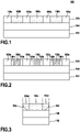
- FIG. 1 illustrates in a cross-section view a conventional layout 100 for embedding a capacitor structure into a porous region.
- the underlying structure may include a substrate 102, a conductive layer 104 above the substrate 104, and a metal layer 106 above the conductive layer 104.
- the metal layer 106 is anodized in defined regions 106b, leaving regions 106a non-anodized. Typically, this is done by applying a hard mask layer (not shown) on top of metal layer 106 to mask the areas corresponding to regions 106a. The masking shields these areas from contact with the anodization electrolyte. The porous region is thus formed in the regions 106b where the hard mask layer is open. Capacitive structures are then embedded into one or more the regions 106b as desired.
- each of regions 106b in fact consists of a region 106c and of two lateral regions 106d.
- the region 106c corresponds to a region in which the pores are well-formed, i.e., they are substantially uniform and extend all the way down to the conductive layer 104. In practice, some of the pores of region 106c may need to be etched at the bottom to ensure they are fully open, but generally these pores are adequate to have a MIM stack deposed into them.
- regions 106d correspond to regions in which the pores are malformed with high probability and, as such, are inadequate for receiving the MIM stack.
- the pore malformation in regions 106d is due to these regions being adjacent to the interfaces between each region 106 and its surrounding regions 106a.
- a hard mask is formed over the defined regions 106a to shield them from anodization.
- the proximity of regions 106d to this hard mask leads to a gradually decreasing anodization electric field in these regions. The closer to the hard mask edge, the weaker the anodization electric field is and the lower the pore formation is.
- MIM deposition and particularly deposition of the conductive M layers, is done using thermal Atomic Layer Deposition (ALD).
- ALD thermal Atomic Layer Deposition
- Precursors for such conductive layer deposition e.g., for conductive materials like TiN, MoN, WN, etc. are chlorine-based and induce corrosion into aluminum.
- the width of the regions 106d is correlated to the thickness of the metal layer 106 being anodized (the thicker the metal layer, the wider the regions 106d). Approximately, the width of the region 106d is 3 times the thickness of the metal layer 106.
- the width of ledge 302 may be reduced by additional control of the anodization process. For example, the process may be allowed to continue a longer time. However, this comes at the risk of weakening the interface between layers 104 and 106, leading to delamination of portions of layer 106. In particular, as the anodization process is allowed to run for a longer time, it becomes difficult to control the oxidization of the layer 104, and particularly to constrain oxidization of the layer 104 in the horizontal direction in between the pores. When the pores are subsequently etched (during a step of opening the bottoms of the pores), the interface between layers 104 and 106 becomes weak causing layer 106 to delaminate.
- regions 106a may be provided in structure 100 in order to form electrical vias to contact, from the top, the bottom electrodes of the capacitive structures embedded into regions 106b. Additionally, some of the regions 106a may be provided at the edges of the wafer in proximity to the dicing lanes, areas of the wafer in which no capacitive structures are built.
- ESR Equivalent Series Resistance
- ESL Equivalent Series Inductance
- ledge 302 (and of regions 106d) however is problematic when a large number of electrical vias are needed in the capacitor structure. Indeed, as shown in FIG. 4 , whenever a region 106a of effective width d1 is present between two porous regions 106b, a width d2, much greater than d1, is needed as regions 106d are lost. In practice, the inventors of the present invention have observed that implementing an electric via of effective width d1 of 15 microns may require up to 100 microns of lateral footprint, as the regions 106d may each be up to 30 microns (and with process overlay rules requiring further spacing).
- FIG. 5 is a top view 500 illustrating the effective capacitance area resulting from the conventional structure 100 of FIG. 1 .
- the area 502 corresponds to the wafer area in which a capacitance structure is built. Area 502 may correspond to the regions 106c described above.
- areas 504 are wafer areas that are not used for capacitance structures. Areas 504 may correspond to the regions 106a and 106d described above.
- the area 506 corresponds to the dicing area of the wafer.
- the effective capacitance area is much lower than the total area of the wafer according to conventional structure 100.
- FIG. 6 illustrates the ratio of the effective capacitance area to the total area as a function of capacitor surface area according to an example implementation.
- the example implementation assumes an effective via width (d1) of 15 microns and a width of 30 microns for each of regions 106d.
- the ratio of effective/total area is below 80% for capacitors smaller than 0.25 mm 2 .
- the ratio decreases to below 70% for capacitors under 0.1 mm 2 and to below 50% for capacitors under 0.04 mm 2 .
- the present invention has been made in the light of the above problems.
- the present invention provides a capacitor structure, comprising:
- the capacitor structure comprises, in the porous layer, both a region for forming a capacitance and a region for providing a via through the capacitor structure.
- the via may be used to contact the conductive layer, which may serve as a bottom of electrode of the capacitor structure.
- both the MIM structure and the via are provided in the same porous layer reduces the lateral footprint of the via within the capacitor structure. As such, the effective utilization of the porous layer as well as the effective capacitance area within the capacitor structure are increased.
- porous regions with residual underlying metal are reduced.
- porous regions may be prone to corrosion, their reduction improves the reliability of the capacitor structure.
- the porous layer comprises a third region which pores are empty, the third region separating the first region and the second region.
- the third region may help keep the MIM structure electrically isolated from the conductive wires.
- the third region with its empty pores may also reduce mechanical stress within the capacitor structure.
- the third region may be immediately adjacent to the first region and immediately adjacent to the second region.
- the third region may thus help satisfy overlay fabrication rules.
- the bottom ends of the pores of the porous layer open onto the conductive layer. This allows for contact between components embedded into the pores and the conductive layer underlying the porous layer.
- the MIM structure disposed in the pores of the second region comprises a first metal layer, disposed conformally into the second region, an insulator layer disposed conformally over the first metal layer, and a second metal layer disposed conformally over the insulator layer.
- the first metal layer contacts the conductive layer at the bottom of each pore of the second region
- the bottom ends of the conductive wires contact the conductive layer at the bottom of the pores of the first region.
- the conductive layer may form the bottom electrode of the capacitor structure.
- the conductive wires form a via through the capacitor structure for contacting the bottom electrode of the capacitor structure.
- the conductive layer comprises a first layer and a second layer, the second layer disposed between the first layer and the porous layer.
- the first layer is made of aluminum, though other metals may be used.
- the second layer is made of tungsten or titanium.
- the second layer serves as an etch barrier layer for protecting the first layer during formation by anodization of the porous layer. This ensures that the first layer is not anodized, ensuring it retains a high conductivity.
- the second layer is discontinuous and open under the first region and/or the second region of the porous layer.
- the opening of the second layer under the first region and/or the second region may be performed to ensure direct contact between the first metal layer of the MIM structure and the conductive layer and/or between the conductive wires and the conductive layer.
- the porous layer is made of anodic aluminum oxide (AAO).
- AAO anodic aluminum oxide
- the substrate may be made of silicon, glass, or a polymer.
- the substrate may be made of silicon and may have a field oxide layer between itself and the conductive layer.
- the conductive layer maybe a composite layer of an aluminum or copper layer and a barrier layer like titanium or tungsten.
- the capacitor structure comprises a metal layer, above the conductive layer, surrounding the porous layer from the sides.
- the metal layer may be a remnant of the initial metal layer that is anodized to form the porous layer.
- the metal layer may surround the edges of the porous layer.
- the metal layer may further comprise islands inside the porous layer.
- the number and position of the metal islands may be chosen by design before anodization to form the porous layer. Specifically, the metal islands are selected to ensure an anodization that is as uniform as possible.
- the capacitor structure comprises a first conductive layer in contact with the MIM structure; and a second conductive layer, isolated from the first conductive layer, in contact with the top ends of the conductive wires.
- the first conductive layer may serve as a top electrode of the capacitor structure.
- the second conductive layer may serve as a contact to the bottom electrode of the capacitor structure.
- the present invention also provides a method of fabricating a capacitor structure, comprising:
- forming the conductive wires in the pores of the first region comprises:
- the conductive wires may be made of nickel or copper.
- forming the MIM structure in the pores of the second region comprises:
- the method also comprises:
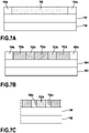
- FIG. 7A illustrates in a cross-section view a proposed layout 700 for embedding a capacitor structure into a porous region according to an embodiment.
- the underlying structure is assumed to include a substrate 102, a conductive layer 104 above the substrate 102, and a metal layer 106 above the conductive layer 104.
- the metal layer 106 may be anodized to form a continuous porous layer 702.
- the continuous porous layer 702 may be designed to extend over the entirety of the wafer surface.
- a wafer-level anodization may be used to obtain the porous layer 702.
- Such an embodiment may be suitable in the case that a uniform anodization across the wafer can be ensured. This can be done by selecting the layer 104 such that it enables a uniform charge distribution across the wafer. In an example experiment, uniform charge distribution across the wafer was obtained using a layer of tungsten of 300 nm as the layer 104.
- regions 106a of the metal layer 106 may be left non-anodized. Regions 106a may be located at the edges of the die and/or in the dicing street (beyond the edge of the die or at the edge of the wafer).
- the metal layer 106 may be left non-anodized in a few islands within the porous layer 702.
- the non-anodized metal islands may be in the form of a sparse metal grid within the porous layer 702.
- Such an embodiment may be suitable in the case that the die is isolated (e.g. by a field oxide) from the wafer backside.
- the non-anodized metal islands help ensure that the anodic voltage is provided in a uniform manner across the wafer.
- the porous layer 702 is then partitioned between regions 702a designed for receiving capacitive structures, and regions 702b designed for serving as electrical vias in the capacitor structure.
- regions 702a a MIM stack may be deposited into the pores.
- conductive wires may be formed in the pores to provide the electrical vias vertically through the structure.
- the conductive wires may be grown using electrochemical deposition (ECD) inside the pores of the regions 702b.
- ECD electrochemical deposition
- the effective utilization of the wafer area is increased substantially. Indeed, as a porous to non-porous transition is no longer needed to implement an electrical via, the via can now be placed much closer to an adjacent functional MIM structure. As such, the lateral footprint of a via can be reduced significantly.
- isolation may be needed between regions 702a and 702b, for example due to process overlay rules.
- a small portion 702c of region 702a e.g., 5-10 microns
- the isolation region neither a MIM structure nor conductive wires are built.
- the pores of the region 702c may be left empty.
- electrical vias may be needed in great numbers in the capacitor structure to provide contact redundancy and/or for ESR/ESL control.
- the proposed layout can thus have a substantial impact on the effective capacitance resulting from the structure.
- Figure 8 is a top view 800 illustrating the effective capacitance area resulting from the proposed layout according to an embodiment.
- the area 802 corresponds to the wafer area in which a capacitance structure is built.
- Area 802 may correspond to the regions 702a shown in FIG. 7B be above.
- areas 804 are wafer areas in which vias are built. Areas 804 may correspond to regions 702b illustrated in FIG. 7B above. In another embodiment, areas 804 may correspond to regions 702b and 702c as shown in FIG. 7c illustrated in FIG. 7C above.
- the area 808 corresponds to the dicing area of the wafer.
- areas 806 corresponding to regions of non-anodized metal may be provided. As mentioned above, these regions may be provided for the purpose of enhancing the anodization process across the wafer. Alternatively, areas 806 may correspond to wafer areas in which vias are built, similar to areas 804.
- the effective capacitive area is significantly increased relative to the total area of the wafer, as compared to the conventional layout illustrated in FIG. 5 .
- FIG. 9 shows the ratio of the effective capacitance area to the total wafer area as a function of capacitor surface area according to an example implementation.
- the line 902 corresponds to performance using the layout of the present invention
- the line 904 corresponds to performance using the conventional layout.
- the utilization ratio increases significantly for all capacitor values. For smaller structures, the increase may be as high as 100%, doubling capacitive density. This kind of improvement may also be observed in a structure with high contact redundancy.
- FIGs. 10A-10K illustrate an example process for producing a capacitor structure in accordance with the proposed layout, according to an embodiment. This example process is provided for the purpose of illustration only and is not limiting of embodiments of the present invention.
- the process begins by forming a stack including a substrate 102, a conductive layer 104 above the substrate, and a metal layer 106 above the conductive layer 106.
- the conductive layer 104 comprises a first layer and a second layer, with the second layer disposed between the first layer and the metal layer 106.
- the first layer is made of aluminum and the second layer is made of tungsten.
- the metal layer 106 may be made of aluminum.
- the process includes anodizing some or all of the metal layer 106 to form a porous layer 108 above the conductive layer 104.
- the porous layer 108 has pores that extend perpendicularly from a top surface of the porous layer 108 toward the conductive layer 104.
- the porous layer 108 is made of anodic aluminum oxide (AAO).
- metal layer 106 is anodized in its entirety. While this embodiment is possible, in practice a small portion of metal layer 106 may be left non-anodized at the edges of the die and/or in the dicing street.
- the porous layer 108 has well-formed pores, i.e., they are substantially uniform and extend all the way down, substantially perpendicularly, to the conductive layer 104.
- an extra etching step may be used to ensure that the pores are fully open onto the conductive layer 104.
- a first hard mask layer 132 is applied over the porous layer 108.
- the first hard mask layer 132 is patterned to have openings over a defined first region 110 of the porous layer 108.
- the material for first hard mask layer 132 may be selected so as to be highly non-conformal to avoid that it enters into the pores of the porous layer 108.
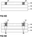
- conductive wires are formed in the pores of the first region 110.
- the conductive wires are grown by electrochemical deposition (ECD).
- the conductive wires may be made of nickel or copper, for example.
- the bottom ends of the conductive wires contact the conductive layer 104 at the bottoms of the pores of the first region 110.
- the first hard mask layer 132 is then removed, and a second hard mask layer 112 is applied and patterned as shown in FIG. 10E .
- the second hard mask layer 110 is patterned so as to cover the first region 110 of the porous layer as well as an adjacent third region 130 of the porous region.
- the third region 130 will serve as an isolation region according to this embodiment.
- a MIM structure is disposed into the pores of a second region 120 of the porous layer 108.
- the second region 120 corresponds to the region of the porous layer 108 that is not covered by the second hard mask 110, i.e., outside of the first region 110 and the third region 130.
- this includes depositing the MIM structure into the porous layer 108 and over the second hard mask 112.
- the top metal layer of the MIM structure may be etched over the first region 110 and the third region 130 as shown in FIG. 10F .
- the MIM structure comprises a first metal layer (114), disposed conformally into the second region (120), an insulator layer (116) disposed conformally over the first metal layer (114), and a second metal layer (118) disposed conformally over the insulator layer (116).
- the first metal layer contacts the conductive layer 104 at the bottom of each pore of the second region 120.
- a first conductive layer 122 may be formed over the MIM structure.
- the first conductive layer 122 may be etched over the first region 110 and the third region 130 as shown in FIG. 10G .
- the first conductive layer 122 may serve as a top electrode of the capacitor structure.
- the MIM structure (the first metal layer 114 and the insulator 116) and the second hard mask 112 are etched over at least a section of the first region 110 of the porous layer. This exposes the top ends of at least some of the conductive wires built into the first region 110 of the porous layer.
- an insulation layer 124 is formed over the first conductive layer 122.
- the insulation layer 124 fully covers (encapsulates) the first conductive layer 122.
- a second conductive layer 126 is formed.
- the second conductive layer 126 covers the exposed section of the first region 110 and at least a portion of the insulation layer 124.
- the second conductive layer 126 is in contact with the exposed top ends of at least some of the conductive wires.
- the second conductive layer may serve as a contact to the bottom electrode of the capacitor structure.
- a passivation layer 128 may be formed over the structure.
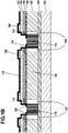
- FIG. 11 illustrates an example capacitor structure 1100 according to an embodiment.
- Example structure 1100 is provided for the purpose of illustration and is not limiting of embodiments.
- Capacitor structure 1100 may be obtained using the process described above.
- capacitor structure 1100 includes a porous layer that comprises a first region 110, a second region 120, and a third region 130.
- conductive wires are disposed in the pores of the porous layer, providing a vertical electrical via through the structure.
- the bottom ends of the conductive wires contact a conductive layer 104 at the bottom of the pores of the first region 110.
- a MIM structure is formed in the pores of the porous layer, providing a capacitor in the structure.
- the third region 130 separates the first region 110 and the second region 120. In embodiment, the third region 130 isolates the first region 110 and the second region 120. In an embodiment, the pores of the third region 130 are empty.
- the conductive layer 104 comprises a first layer and a second layer, the second layer disposed between the first layer and the porous layer.
- the second layer is discontinuous and open under the first region 110 and/or the second region 120 of the porous layer.
Landscapes
- Engineering & Computer Science (AREA)
- Power Engineering (AREA)
- Microelectronics & Electronic Packaging (AREA)
- Manufacturing & Machinery (AREA)
- Chemical & Material Sciences (AREA)
- Inorganic Chemistry (AREA)
- Semiconductor Integrated Circuits (AREA)
Abstract
Description
- The present invention relates to the field of integration and, more particularly, to electronic products, related semiconductor products, and their methods of manufacture.
- Silicon passive integration technologies are nowadays accessible for industrial design. For example, the PICS technology developed by Murata Integrated Passive Solutions allows integrating high density capacitive components into a silicon substrate. According to this technology, tens or even hundreds of passive components can be efficiently integrated into a silicon die.
- In their work titled "Nanotubular metal-insulator-metal capacitor arrays for energy storage" (published in Natural technology, May 2009), P. Banerjee et al. describe a metal-insulator-metal (MIM) structure formed in a porous anodic material, such as porous anodic alumina (PAA) for example. The successive layers of metal, insulator, and then metal follow the contours of the porous material resulting in the MIM structure being embedded inside the pores of the porous material. Banerjee's PAA embedded structure however suffers from high Equivalent Series Resistance (ESR) and limited capacitance density due to the PAA thickness that can be deposited by Atomic Layer Deposition (ALD).
- A structure by F. Voiron et al. that improves Banerjee's ESR and capacitance is described in international application publication
WO 2015/063420 A1 . Voiron's structure results in highly integrated capacitance that may be used in a variety of applications. In this structure the bottoms of the pores are opened and the lower metal layer of the MIM structure contacts a conductive layer that underlies the porous region, providing electrical contact and reducing ESR. - Generally, PAA embedded structures as described above result from embedding a structure (e.g., a MIM capacitive stack) inside a porous region above a substrate, such as a silicon wafer. Typically, the porous region results from anodizing a layer of metal, such as aluminum, deposited above the substrate. The anodization converts the aluminum layer into porous anodic alumina. Typically, the porous region is formed with any shape (as viewed from the top) and extends across the alumina layer in a direction perpendicular to the wafer surface.
-
FIG. 1 illustrates in a cross-section view aconventional layout 100 for embedding a capacitor structure into a porous region. The underlying structure may include asubstrate 102, aconductive layer 104 above thesubstrate 104, and ametal layer 106 above theconductive layer 104. - According to the
conventional layout 100, themetal layer 106 is anodized indefined regions 106b, leavingregions 106a non-anodized. Typically, this is done by applying a hard mask layer (not shown) on top ofmetal layer 106 to mask the areas corresponding toregions 106a. The masking shields these areas from contact with the anodization electrolyte. The porous region is thus formed in theregions 106b where the hard mask layer is open. Capacitive structures are then embedded into one or more theregions 106b as desired. - In practice, however, the effective structure resulting the conventional layout of
FIG. 1 is different. Indeed, as shown inFIG. 2 , and in more detail inFIG. 3 , each ofregions 106b in fact consists of aregion 106c and of twolateral regions 106d. - The
region 106c corresponds to a region in which the pores are well-formed, i.e., they are substantially uniform and extend all the way down to theconductive layer 104. In practice, some of the pores ofregion 106c may need to be etched at the bottom to ensure they are fully open, but generally these pores are adequate to have a MIM stack deposed into them. - In contrast, the
regions 106d correspond to regions in which the pores are malformed with high probability and, as such, are inadequate for receiving the MIM stack. - The pore malformation in
regions 106d is due to these regions being adjacent to the interfaces between eachregion 106 and its surroundingregions 106a. In fact, as mentioned above, during anodization, a hard mask is formed over thedefined regions 106a to shield them from anodization. The proximity ofregions 106d to this hard mask leads to a gradually decreasing anodization electric field in these regions. The closer to the hard mask edge, the weaker the anodization electric field is and the lower the pore formation is. - The effect of this phenomenon is that the pores in
regions 106d stop in aresidual aluminum ledge 302, rather than extending all the way down to theconductive layer 104. The fact that the pores inregions 106d end inledge 302 is another reason for them being inadequate for receiving the MIM stack. In practice, MIM deposition, and particularly deposition of the conductive M layers, is done using thermal Atomic Layer Deposition (ALD). Precursors for such conductive layer deposition (e.g., for conductive materials like TiN, MoN, WN, etc.) are chlorine-based and induce corrosion into aluminum. - In practice, the width of the
regions 106d is correlated to the thickness of themetal layer 106 being anodized (the thicker the metal layer, the wider theregions 106d). Approximately, the width of theregion 106d is 3 times the thickness of themetal layer 106. - The width of ledge 302 (and of
regions 106d) may be reduced by additional control of the anodization process. For example, the process may be allowed to continue a longer time. However, this comes at the risk of weakening the interface betweenlayers layer 106. In particular, as the anodization process is allowed to run for a longer time, it becomes difficult to control the oxidization of thelayer 104, and particularly to constrain oxidization of thelayer 104 in the horizontal direction in between the pores. When the pores are subsequently etched (during a step of opening the bottoms of the pores), the interface betweenlayers layer 106 to delaminate. - In implementation, some of
regions 106a may be provided instructure 100 in order to form electrical vias to contact, from the top, the bottom electrodes of the capacitive structures embedded intoregions 106b. Additionally, some of theregions 106a may be provided at the edges of the wafer in proximity to the dicing lanes, areas of the wafer in which no capacitive structures are built. - It is usually desirable to provide contact redundancy by providing several vias to contact a given bottom electrode. In addition, in some cases, the addition of electrical vias may be needed to improve electrical performance. For example, it is desired to reduce the Equivalent Series Resistance (ESR) and the Equivalent Series Inductance (ESL) of the capacitor structure. The addition of electrical vias can help reduce both ESR and ESL. This is particularly true for smaller size capacitors (e.g., below ¼ mm2) where capacitance parallelization is lower than for greater size capacitor structures.
- The presence of ledge 302 (and of
regions 106d) however is problematic when a large number of electrical vias are needed in the capacitor structure. Indeed, as shown inFIG. 4 , whenever aregion 106a of effective width d1 is present between twoporous regions 106b, a width d2, much greater than d1, is needed asregions 106d are lost. In practice, the inventors of the present invention have observed that implementing an electric via of effective width d1 of 15 microns may require up to 100 microns of lateral footprint, as theregions 106d may each be up to 30 microns (and with process overlay rules requiring further spacing). -
FIG. 5 is atop view 500 illustrating the effective capacitance area resulting from theconventional structure 100 ofFIG. 1 . In particular, thearea 502 corresponds to the wafer area in which a capacitance structure is built.Area 502 may correspond to theregions 106c described above. Conversely,areas 504 are wafer areas that are not used for capacitance structures.Areas 504 may correspond to theregions area 506 corresponds to the dicing area of the wafer. - As shown in
FIG. 5 , the effective capacitance area is much lower than the total area of the wafer according toconventional structure 100. This is further shown inFIG. 6 , which illustrates the ratio of the effective capacitance area to the total area as a function of capacitor surface area according to an example implementation. The example implementation assumes an effective via width (d1) of 15 microns and a width of 30 microns for each ofregions 106d. - As shown, the ratio of effective/total area is below 80% for capacitors smaller than 0.25 mm2. The ratio decreases to below 70% for capacitors under 0.1 mm2 and to below 50% for capacitors under 0.04 mm2.
- The present invention has been made in the light of the above problems.
- The present invention provides a capacitor structure, comprising:
- a substrate;
- a conductive layer above the substrate; and
- a porous layer, above the conductive layer, having pores that extend perpendicularly from a top surface of the porous layer toward the conductive layer,
- characterized in that the porous layer comprises a first region in which pores conductive wires are disposed, and a second region in which pores a metal-insulator-metal (MIM) structure is disposed.
- The conductive wires form a via through the capacitor structure. As such, the capacitor structure comprises, in the porous layer, both a region for forming a capacitance and a region for providing a via through the capacitor structure.
- The via may be used to contact the conductive layer, which may serve as a bottom of electrode of the capacitor structure.
- The fact that both the MIM structure and the via are provided in the same porous layer reduces the lateral footprint of the via within the capacitor structure. As such, the effective utilization of the porous layer as well as the effective capacitance area within the capacitor structure are increased.
- In addition, as transitions from porous to non-porous regions (e.g., non-anodized metal) within the capacitor structure are reduced, porous regions with residual underlying metal are reduced. As such porous regions may be prone to corrosion, their reduction improves the reliability of the capacitor structure.
- In an embodiment, the porous layer comprises a third region which pores are empty, the third region separating the first region and the second region. The third region may help keep the MIM structure electrically isolated from the conductive wires. The third region with its empty pores may also reduce mechanical stress within the capacitor structure.
- The third region may be immediately adjacent to the first region and immediately adjacent to the second region. The third region may thus help satisfy overlay fabrication rules.
- In an embodiment, the bottom ends of the pores of the porous layer open onto the conductive layer. This allows for contact between components embedded into the pores and the conductive layer underlying the porous layer.
- In an embodiment, the MIM structure disposed in the pores of the second region comprises a first metal layer, disposed conformally into the second region, an insulator layer disposed conformally over the first metal layer, and a second metal layer disposed conformally over the insulator layer. The first metal layer contacts the conductive layer at the bottom of each pore of the second region
- In an embodiment, the bottom ends of the conductive wires contact the conductive layer at the bottom of the pores of the first region. The conductive layer may form the bottom electrode of the capacitor structure. As such, the conductive wires form a via through the capacitor structure for contacting the bottom electrode of the capacitor structure.
- In an embodiment, the conductive layer comprises a first layer and a second layer, the second layer disposed between the first layer and the porous layer.
- In an embodiment, the first layer is made of aluminum, though other metals may be used.
- In an embodiment, the second layer is made of tungsten or titanium. In an embodiment, the second layer serves as an etch barrier layer for protecting the first layer during formation by anodization of the porous layer. This ensures that the first layer is not anodized, ensuring it retains a high conductivity.
- In an embodiment, the second layer is discontinuous and open under the first region and/or the second region of the porous layer. The opening of the second layer under the first region and/or the second region may be performed to ensure direct contact between the first metal layer of the MIM structure and the conductive layer and/or between the conductive wires and the conductive layer.
- In an embodiment, the porous layer is made of anodic aluminum oxide (AAO).
- In an embodiment, the substrate may be made of silicon, glass, or a polymer.
- In another embodiment, the substrate may be made of silicon and may have a field oxide layer between itself and the conductive layer. The conductive layer maybe a composite layer of an aluminum or copper layer and a barrier layer like titanium or tungsten.
- In an embodiment, the capacitor structure comprises a metal layer, above the conductive layer, surrounding the porous layer from the sides. The metal layer may be a remnant of the initial metal layer that is anodized to form the porous layer. The metal layer may surround the edges of the porous layer.
- In another embodiment, the metal layer may further comprise islands inside the porous layer. The number and position of the metal islands may be chosen by design before anodization to form the porous layer. Specifically, the metal islands are selected to ensure an anodization that is as uniform as possible.
- In an embodiment, the capacitor structure comprises
a first conductive layer in contact with the MIM structure; and
a second conductive layer, isolated from the first conductive layer, in contact with the top ends of the conductive wires. - The first conductive layer may serve as a top electrode of the capacitor structure. The second conductive layer may serve as a contact to the bottom electrode of the capacitor structure.
- In another aspect, the present invention also provides a method of fabricating a capacitor structure, comprising:
- forming a porous layer above a conductive layer, the porous layer having pores that extend perpendicularly from a top surface of the porous layer toward the conductive layer;
- forming conductive wires in the pores of a first region of the porous layer, the bottom ends of the conductive wires contacting the conductive layer at the bottoms of the pores of the first region;
- forming a metal-insulator-metal (MIM) structure in the pores of a second region of the porous layer;
- In an embodiment, forming the conductive wires in the pores of the first region comprises:
- depositing a first hard mask over the porous layer, the first hard mask being open over the first region;
- growing the conductive wires in the pores of the first region by electro-chemical deposition (ECD).
- In an embodiment, the conductive wires may be made of nickel or copper.
- In an embodiment, forming the MIM structure in the pores of the second region comprises:
- removing the first hard mask;
- depositing a second hard mask covering the first region and an adjacent third region (130) of the porous layer; and
- depositing the MIM structure into the porous layer and the second hard mask.
- In an embodiment, the method also comprises:
- forming a first conductive layer over the MIM structure;
- etching the MIM structure and the second hard mask over at least a section of the first region to expose the top ends of at least some of the conductive wires;
- forming an insulation layer over the first conductive layer, the insulator layer fully covering the first conductive layer; and
- forming a second conductive layer over the top-end exposed conductive wires and at least a portion of the insulation layer, the second conductive layer in contact with the top ends of said at least some of the conductive wires.
- Further features and advantages of the present invention will become apparent from the following description of certain embodiments thereof, given by way of illustration only, not limitation, with reference to the accompanying drawings in which:
-
FIG. 1 illustrates in a cross-section view a conventional layout for embedding a capacitor structure into a porous template; -
FIG. 2 illustrates in a cross-section view the effective structure resulting from the conventional structure offigure 1 ; -
FIG. 3 shows an enlarged view of a section of the effective structure ofFIG. 2 ; -
FIG. 4 shows in a cross-section view a via formed in the effective structure ofFIG. 2 ; -
FIG. 5 is a top view illustrates the effective capacitance area resulting from the conventional structure ofFIG. 1 ; -
FIG. 6 illustrates the ratio of the effective capacitance area to the total area as a function of capacitor surface area for the convention structure ofFIG. 1 ; -
FIGs. 7A-7C illustrate in a cross-section view a proposed layout for embedding a capacitor structure into a porous template according to an embodiment; -
FIG. 8 illustrates the effective capacitance area resulting from the proposed layout according to an environment; -
FIG. 9 illustrates the impact of the proposed layout on the ratio of net to raw capacitance; -
FIGs. 10A-10K illustrate a process for producing a capacitor structure in accordance with the proposed layout, according to an embodiment; -
FIG. 11 illustrates an example capacitor structure according to an environment. -
FIG. 7A illustrates in a cross-section view a proposed layout 700 for embedding a capacitor structure into a porous region according to an embodiment. As above, the underlying structure is assumed to include asubstrate 102, aconductive layer 104 above thesubstrate 102, and ametal layer 106 above theconductive layer 104. - As shown in
FIG. 7A , rather than defining, within themetal layer 106, interleaving anodized and non-anodized regions, themetal layer 106 may be anodized to form a continuousporous layer 702. - In an embodiment, the continuous
porous layer 702 may be designed to extend over the entirety of the wafer surface. For example, in one implementation, a wafer-level anodization may be used to obtain theporous layer 702. Such an embodiment may be suitable in the case that a uniform anodization across the wafer can be ensured. This can be done by selecting thelayer 104 such that it enables a uniform charge distribution across the wafer. In an example experiment, uniform charge distribution across the wafer was obtained using a layer of tungsten of 300 nm as thelayer 104. - In another embodiment, as shown in
FIG. 7A ,certain regions 106a of themetal layer 106 may be left non-anodized.Regions 106a may be located at the edges of the die and/or in the dicing street (beyond the edge of the die or at the edge of the wafer). - In another environment, the
metal layer 106 may be left non-anodized in a few islands within theporous layer 702. The non-anodized metal islands may be in the form of a sparse metal grid within theporous layer 702. Such an embodiment may be suitable in the case that the die is isolated (e.g. by a field oxide) from the wafer backside. The non-anodized metal islands help ensure that the anodic voltage is provided in a uniform manner across the wafer. - As shown in
FIG. 7B , theporous layer 702 is then partitioned betweenregions 702a designed for receiving capacitive structures, andregions 702b designed for serving as electrical vias in the capacitor structure. In theregions 702a, a MIM stack may be deposited into the pores. In theregions 702b, conductive wires may be formed in the pores to provide the electrical vias vertically through the structure. In an embodiment, the conductive wires may be grown using electrochemical deposition (ECD) inside the pores of theregions 702b. - By using the layout 700, the effective utilization of the wafer area is increased substantially. Indeed, as a porous to non-porous transition is no longer needed to implement an electrical via, the via can now be placed much closer to an adjacent functional MIM structure. As such, the lateral footprint of a via can be reduced significantly.
- In practice, some isolation may be needed between
regions FIG. 7C , when aregion 702a is adjacent to aregion 702b in which a via is to be built, asmall portion 702c ofregion 702a (e.g., 5-10 microns) may be designated as an isolation region. In the isolation region, neither a MIM structure nor conductive wires are built. In an embodiment, the pores of theregion 702c may be left empty. - However, the lateral footprint of a via remains very small. In experiments, the inventors have observed that an electric via with an effective width of 15 microns may require a lateral footprint of only 27 microns. This may be reduced further with better photolithographic alignment.
- As mentioned above, electrical vias may be needed in great numbers in the capacitor structure to provide contact redundancy and/or for ESR/ESL control. By substantially reducing the lateral footprint of a via, the proposed layout can thus have a substantial impact on the effective capacitance resulting from the structure.
-
Figure 8 is atop view 800 illustrating the effective capacitance area resulting from the proposed layout according to an embodiment. In particular, thearea 802 corresponds to the wafer area in which a capacitance structure is built.Area 802 may correspond to theregions 702a shown inFIG. 7B be above. Conversely,areas 804 are wafer areas in which vias are built.Areas 804 may correspond toregions 702b illustrated inFIG. 7B above. In another embodiment,areas 804 may correspond toregions FIG. 7c illustrated inFIG. 7C above. Thearea 808 corresponds to the dicing area of the wafer. - Optionally,
areas 806 corresponding to regions of non-anodized metal may be provided. As mentioned above, these regions may be provided for the purpose of enhancing the anodization process across the wafer. Alternatively,areas 806 may correspond to wafer areas in which vias are built, similar toareas 804. - As shown in
FIG. 8 , the effective capacitive area is significantly increased relative to the total area of the wafer, as compared to the conventional layout illustrated inFIG. 5 . This is further illustrated inFIG. 9 , which shows the ratio of the effective capacitance area to the total wafer area as a function of capacitor surface area according to an example implementation. Particularly, inFIG. 9 , theline 902 corresponds to performance using the layout of the present invention, whereas theline 904 corresponds to performance using the conventional layout. As shown, the utilization ratio increases significantly for all capacitor values. For smaller structures, the increase may be as high as 100%, doubling capacitive density. This kind of improvement may also be observed in a structure with high contact redundancy. -
FIGs. 10A-10K illustrate an example process for producing a capacitor structure in accordance with the proposed layout, according to an embodiment. This example process is provided for the purpose of illustration only and is not limiting of embodiments of the present invention. - As shown in
FIG. 10A , the process begins by forming a stack including asubstrate 102, aconductive layer 104 above the substrate, and ametal layer 106 above theconductive layer 106. - In an embodiment, the
conductive layer 104 comprises a first layer and a second layer, with the second layer disposed between the first layer and themetal layer 106. In an embodiment, the first layer is made of aluminum and the second layer is made of tungsten. Themetal layer 106 may be made of aluminum. - Next, as shown in
FIG. 10B , the process includes anodizing some or all of themetal layer 106 to form aporous layer 108 above theconductive layer 104. Theporous layer 108 has pores that extend perpendicularly from a top surface of theporous layer 108 toward theconductive layer 104. When themetal layer 106 is made of aluminum, theporous layer 108 is made of anodic aluminum oxide (AAO). - In
FIG. 10B , it is illustrated that themetal layer 106 is anodized in its entirety. While this embodiment is possible, in practice a small portion ofmetal layer 106 may be left non-anodized at the edges of the die and/or in the dicing street. - Because of the proposed layout, a uniform anodization can be obtained across the wafer. As such, the
porous layer 108 has well-formed pores, i.e., they are substantially uniform and extend all the way down, substantially perpendicularly, to theconductive layer 104. In practice, an extra etching step may be used to ensure that the pores are fully open onto theconductive layer 104. - Next, as shown in
FIG. 10C , a firsthard mask layer 132 is applied over theporous layer 108. The firsthard mask layer 132 is patterned to have openings over a definedfirst region 110 of theporous layer 108. - Preferably, the material for first
hard mask layer 132 may be selected so as to be highly non-conformal to avoid that it enters into the pores of theporous layer 108. - Subsequently, as shown in
FIG. 10D , conductive wires are formed in the pores of thefirst region 110. In an embodiment, the conductive wires are grown by electrochemical deposition (ECD). The conductive wires may be made of nickel or copper, for example. In an embodiment, the bottom ends of the conductive wires contact theconductive layer 104 at the bottoms of the pores of thefirst region 110. - The first
hard mask layer 132 is then removed, and a secondhard mask layer 112 is applied and patterned as shown inFIG. 10E . Specifically, the secondhard mask layer 110 is patterned so as to cover thefirst region 110 of the porous layer as well as an adjacentthird region 130 of the porous region. As further described below, thethird region 130 will serve as an isolation region according to this embodiment. - Next, as shown in
FIG. 10F , a MIM structure is disposed into the pores of asecond region 120 of theporous layer 108. According to this embodiment, thesecond region 120 corresponds to the region of theporous layer 108 that is not covered by the secondhard mask 110, i.e., outside of thefirst region 110 and thethird region 130. - In an embodiment, this includes depositing the MIM structure into the
porous layer 108 and over the secondhard mask 112. In an embodiment, the top metal layer of the MIM structure may be etched over thefirst region 110 and thethird region 130 as shown inFIG. 10F . - The deposition of the MIM structure into the pores of the
second region 120 is highly conformal. In an embodiment, the MIM structure comprises a first metal layer (114), disposed conformally into the second region (120), an insulator layer (116) disposed conformally over the first metal layer (114), and a second metal layer (118) disposed conformally over the insulator layer (116). In an embodiment, the first metal layer contacts theconductive layer 104 at the bottom of each pore of thesecond region 120. - Next, as shown in
FIG. 10G , a firstconductive layer 122 may be formed over the MIM structure. The firstconductive layer 122 may be etched over thefirst region 110 and thethird region 130 as shown inFIG. 10G . In an embodiment, the firstconductive layer 122 may serve as a top electrode of the capacitor structure. - Subsequently, as shown in
FIG. 10H , the MIM structure (thefirst metal layer 114 and the insulator 116) and the secondhard mask 112 are etched over at least a section of thefirst region 110 of the porous layer. This exposes the top ends of at least some of the conductive wires built into thefirst region 110 of the porous layer. - Next, as shown in
FIG. 10I , aninsulation layer 124 is formed over the firstconductive layer 122. Theinsulation layer 124 fully covers (encapsulates) the firstconductive layer 122. - Then, as shown in
FIG. 10J , a secondconductive layer 126 is formed. The secondconductive layer 126 covers the exposed section of thefirst region 110 and at least a portion of theinsulation layer 124. The secondconductive layer 126 is in contact with the exposed top ends of at least some of the conductive wires. In an embodiment, the second conductive layer may serve as a contact to the bottom electrode of the capacitor structure. - Finally, as shown in
FIG. 10K , apassivation layer 128 may be formed over the structure. -
FIG. 11 illustrates anexample capacitor structure 1100 according to an embodiment.Example structure 1100 is provided for the purpose of illustration and is not limiting of embodiments.Capacitor structure 1100 may be obtained using the process described above. - As shown,
capacitor structure 1100 includes a porous layer that comprises afirst region 110, asecond region 120, and athird region 130. - In the
first region 110, conductive wires are disposed in the pores of the porous layer, providing a vertical electrical via through the structure. The bottom ends of the conductive wires contact aconductive layer 104 at the bottom of the pores of thefirst region 110. - In the
second region 120, a MIM structure is formed in the pores of the porous layer, providing a capacitor in the structure. - The
third region 130 separates thefirst region 110 and thesecond region 120. In embodiment, thethird region 130 isolates thefirst region 110 and thesecond region 120. In an embodiment, the pores of thethird region 130 are empty. - In an embodiment, the
conductive layer 104 comprises a first layer and a second layer, the second layer disposed between the first layer and the porous layer. In an embodiment, the second layer is discontinuous and open under thefirst region 110 and/or thesecond region 120 of the porous layer. - Although the present invention has been described above with reference to certain specific embodiments, it will be understood that the invention is not limited by the particularities of the specific embodiments. Numerous variations, modifications and developments may be made in the above-described embodiments within the scope of the appended claims.
Claims (15)
- A capacitor structure (1100), comprising:a substrate (102);a conductive layer (104) above the substrate (102); anda porous layer, above the conductive layer (104), having pores that extend perpendicularly from a top surface of the porous layer toward the conductive layer (104),characterized in that the porous layer comprises a first region (110) in which pores conductive wires are disposed, and a second region (120) in which pores a metal-insulator-metal (MIM) structure is disposed.
- The capacitor structure (1100) of claim 1, wherein the porous layer comprises a third region (130) which pores are empty, the third region (130) separating the first region (110) and the second region (120).
- The capacitor structure (1100) of claim 1, wherein the third region (130) is immediately adjacent to the first region (110) and immediately adjacent to the second region (120).
- The capacitor structure (1100) of any of claims 1-3, wherein the MIM structure disposed in the pores of the second region (120) comprises a first metal layer, disposed conformally into the second region (120), an insulator layer disposed conformally over the first metal layer, and a second metal layer disposed conformally over the insulator layer, and wherein the first metal layer contacts the conductive layer (104) at the bottom of each pore of the second region (120).
- The capacitor structure (1100) of any of claims 1-4, wherein the bottom ends of the conductive wires contact the conductive layer (104) at the bottom of the pores of the first region (110).
- The capacitor structure (1100) of any of claims 1-5, wherein the conductive layer (104) comprises a first layer and a second layer, the second layer disposed between the first layer and the porous layer.
- The capacitor structure (1100) of claim 6, wherein the first layer is made of aluminum and the second layer is made of tungsten.
- The capacitor structure (100) of claim 6, wherein the second layer is discontinuous and open under the first region (110) and/or the second region (120) of the porous layer.
- The capacitor structure (100) of any of claims 1-8, wherein the porous layer is made of anodic aluminum oxide (AAO).
- The capacitor structure (100) of any of claims 1-9, comprising:
a metal layer (106a), above the conductive layer (104), surrounding the porous layer from the sides. - The capacitor structure (100) of any of claims 1-10, comprising:a first conductive layer (122) in contact with the MIM structure; anda second conductive layer (124), isolated from the first conductive layer (122), in contact with the top ends of the conductive wires.
- A method of fabricating a capacitor structure, comprising:forming a porous layer (108) above a conductive layer (104), the porous layer (108) having pores that extend perpendicularly from a top surface of the porous layer (108) toward the conductive layer (104);forming conductive wires in the pores of a first region (110) of the porous layer, the bottom ends of the conductive wires contacting the conductive layer (104) at the bottoms of the pores of the first region (110);forming a metal-insulator-metal (MIM) structure in the pores of a second region (120) of the porous layer;
- The method of claim 12, wherein forming the conductive wires in the pores of the first region (110) comprises:depositing a first hard mask (132) over the porous layer (108), the first hard mask (132) being open over the first region (110);growing the conductive wires in the pores of the first region (110) by electro-chemical deposition (ECD).
- The method of claim 13, wherein forming the MIM structure in the pores of the second region (120) comprises:removing the first hard mask (132);depositing a second hard mask (112) covering the first region (110) and an adjacent third region (130) of the porous layer (108); anddepositing the MIM structure into the porous layer (108) and over the second hard mask (112).
- The method of claim 14, comprising:forming a first conductive layer (122) over the MIM structure;etching the MIM structure and the second hard mask (112) over a section of the first region (110) to expose the first region (110) in said section;forming an insulation layer (124) over the first conductive layer (122), the insulator layer (124) fully covering the first conductive layer (122); andforming a second conductive layer (126) over the exposed section of the first region (110) and at least a portion of the insulation layer (124), the second conductive layer (126) in contact with the top ends of said at least some of the conductive wires.
Priority Applications (4)
| Application Number | Priority Date | Filing Date | Title |
|---|---|---|---|
| EP20306479.5A EP4009340B1 (en) | 2020-12-02 | 2020-12-02 | Capacitor structure with via embedded in porous medium |
| TW110139900A TWI884329B (en) | 2020-12-02 | 2021-10-27 | Capacitor structure with via embedded in porous medium and a method of fabricating such a capacitor structure |
| PCT/IB2021/060801 WO2022118133A1 (en) | 2020-12-02 | 2021-11-22 | Capacitor structure with via embedded in porous medium |
| US18/328,059 US12431291B2 (en) | 2020-12-02 | 2023-06-02 | Capacitor structure with via embedded in porous medium |
Applications Claiming Priority (1)
| Application Number | Priority Date | Filing Date | Title |
|---|---|---|---|
| EP20306479.5A EP4009340B1 (en) | 2020-12-02 | 2020-12-02 | Capacitor structure with via embedded in porous medium |
Publications (2)
| Publication Number | Publication Date |
|---|---|
| EP4009340A1 true EP4009340A1 (en) | 2022-06-08 |
| EP4009340B1 EP4009340B1 (en) | 2023-06-28 |
Family
ID=73839000
Family Applications (1)
| Application Number | Title | Priority Date | Filing Date |
|---|---|---|---|
| EP20306479.5A Active EP4009340B1 (en) | 2020-12-02 | 2020-12-02 | Capacitor structure with via embedded in porous medium |
Country Status (4)
| Country | Link |
|---|---|
| US (1) | US12431291B2 (en) |
| EP (1) | EP4009340B1 (en) |
| TW (1) | TWI884329B (en) |
| WO (1) | WO2022118133A1 (en) |
Cited By (1)
| Publication number | Priority date | Publication date | Assignee | Title |
|---|---|---|---|---|
| EP4668314A1 (en) | 2024-06-17 | 2025-12-24 | pSemi Corporation | An electrical device for measuring an electrical parameter of a conductive layer to be characterized including multiple 2d capacitors |
Families Citing this family (2)
| Publication number | Priority date | Publication date | Assignee | Title |
|---|---|---|---|---|
| US12573553B2 (en) * | 2023-11-27 | 2026-03-10 | Dell Products L.P. | Selectively enhancing the resonance frequency and quality factor of on-chip capacitors |
| US20250364183A1 (en) * | 2024-05-21 | 2025-11-27 | Dell Products L.P. | Enhancing the quality factor of planar capacitors without impacting the resonance frequency |
Citations (3)
| Publication number | Priority date | Publication date | Assignee | Title |
|---|---|---|---|---|
| WO2015063420A1 (en) | 2013-10-29 | 2015-05-07 | Ipdia | Structure with an improved capacitor |
| US20170316881A1 (en) * | 2016-04-29 | 2017-11-02 | The Regents Of The University Of California | Electronic substrates and interposers made from nanoporous films |
| EP3680931A1 (en) * | 2019-01-08 | 2020-07-15 | Murata Manufacturing Co., Ltd. | Method for forming product structure having porous regions and lateral encapsulation |
Family Cites Families (9)
| Publication number | Priority date | Publication date | Assignee | Title |
|---|---|---|---|---|
| US6689643B2 (en) * | 2002-04-25 | 2004-02-10 | Chartered Semiconductor Manufacturing Ltd. | Adjustable 3D capacitor |
| US8385046B2 (en) * | 2006-11-01 | 2013-02-26 | The Arizona Board Regents | Nano scale digitated capacitor |
| JP5330376B2 (en) * | 2007-05-10 | 2013-10-30 | アイピーディーアイエイ | Integrated device, method of manufacturing the same, and system-in-package |
| WO2009078225A1 (en) * | 2007-12-14 | 2009-06-25 | Murata Manufacturing Co., Ltd. | Method for fabricating thin-film laminated capacitor |
| JP5460155B2 (en) * | 2009-07-14 | 2014-04-02 | 新光電気工業株式会社 | Capacitor and wiring board |
| JP5931594B2 (en) * | 2012-06-07 | 2016-06-08 | 太陽誘電株式会社 | Capacitor |
| US9991333B1 (en) * | 2017-02-09 | 2018-06-05 | Taiwan Semiconductor Manufacturing Co., Ltd. | Metal-insulator-metal (MIM) capacitor structure and method for forming the same |
| EP3570307A1 (en) * | 2018-05-18 | 2019-11-20 | Murata Manufacturing Co., Ltd. | Integrated energy storage component |
| JP2021114531A (en) * | 2020-01-17 | 2021-08-05 | 株式会社村田製作所 | Semiconductor device |
-
2020
- 2020-12-02 EP EP20306479.5A patent/EP4009340B1/en active Active
-
2021
- 2021-10-27 TW TW110139900A patent/TWI884329B/en active
- 2021-11-22 WO PCT/IB2021/060801 patent/WO2022118133A1/en not_active Ceased
-
2023
- 2023-06-02 US US18/328,059 patent/US12431291B2/en active Active
Patent Citations (3)
| Publication number | Priority date | Publication date | Assignee | Title |
|---|---|---|---|---|
| WO2015063420A1 (en) | 2013-10-29 | 2015-05-07 | Ipdia | Structure with an improved capacitor |
| US20170316881A1 (en) * | 2016-04-29 | 2017-11-02 | The Regents Of The University Of California | Electronic substrates and interposers made from nanoporous films |
| EP3680931A1 (en) * | 2019-01-08 | 2020-07-15 | Murata Manufacturing Co., Ltd. | Method for forming product structure having porous regions and lateral encapsulation |
Non-Patent Citations (1)
| Title |
|---|
| P. BANERJEE: "Natural technology", May 2009, article "Nanotubular metal-insulator-metal capacitor arrays for energy storage" |
Cited By (2)
| Publication number | Priority date | Publication date | Assignee | Title |
|---|---|---|---|---|
| EP4668314A1 (en) | 2024-06-17 | 2025-12-24 | pSemi Corporation | An electrical device for measuring an electrical parameter of a conductive layer to be characterized including multiple 2d capacitors |
| WO2025262543A1 (en) | 2024-06-17 | 2025-12-26 | Psemi Corporation | Method for manufacturing an integrated device comprising an anodizable layer |
Also Published As
| Publication number | Publication date |
|---|---|
| WO2022118133A1 (en) | 2022-06-09 |
| WO2022118133A4 (en) | 2022-08-11 |
| EP4009340B1 (en) | 2023-06-28 |
| US20230307185A1 (en) | 2023-09-28 |
| TWI884329B (en) | 2025-05-21 |
| US12431291B2 (en) | 2025-09-30 |
| TW202223948A (en) | 2022-06-16 |
Similar Documents
| Publication | Publication Date | Title |
|---|---|---|
| US11316006B2 (en) | Porous region structure and method of manufacture thereof | |
| US12371808B2 (en) | Method for forming product structure having porous regions and lateral encapsulation | |
| US12431291B2 (en) | Capacitor structure with via embedded in porous medium | |
| TWI819150B (en) | Nanowire structure enhanced for stack deposition and methods of manufacturing electronic products including the same | |
| US20230138497A1 (en) | Nanowire array structures for integration, products incorporating the structures, and methods of manufacture thereof | |
| US12336241B2 (en) | Manufacturing method of a nanowire-based structure and capacitor array component including the structure | |
| US20240321946A1 (en) | Integrated device having plugged up pores in an island or a protuberance, and corresponding method | |
| US20240213018A1 (en) | Method of manufacturing an integrated device compising anodic porous oxide with limited roughness | |
| US12406811B2 (en) | Device having an anodic porous region surrounded by a trench having an electrical isolation barrier | |
| EP4730946A1 (en) | Method of forming an integrated device by patterning a barrier after anodization | |
| EP4432812A1 (en) | Method of forming an integrated device with multiple capacitors by patterning a barrier after anodization | |
| CN116601729A (en) | Capacitor structure with vias embedded in porous media | |
| EP4668314A1 (en) | An electrical device for measuring an electrical parameter of a conductive layer to be characterized including multiple 2d capacitors | |
| US12476051B2 (en) | High-density capacitive device and method for manufacturing such a device | |
| EP4738402A1 (en) | Electrical device comprising a capacitor formed using a porous structure and conductive wires | |
| EP4641598A1 (en) | An energy storage component comprising a capacitor or an ionic capacitor, with a buffer layer in a peripheral region |
Legal Events
| Date | Code | Title | Description |
|---|---|---|---|
| PUAI | Public reference made under article 153(3) epc to a published international application that has entered the european phase |
Free format text: ORIGINAL CODE: 0009012 |
|
| STAA | Information on the status of an ep patent application or granted ep patent |
Free format text: STATUS: THE APPLICATION HAS BEEN PUBLISHED |
|
| AK | Designated contracting states |
Kind code of ref document: A1 Designated state(s): AL AT BE BG CH CY CZ DE DK EE ES FI FR GB GR HR HU IE IS IT LI LT LU LV MC MK MT NL NO PL PT RO RS SE SI SK SM TR |
|
| STAA | Information on the status of an ep patent application or granted ep patent |
Free format text: STATUS: REQUEST FOR EXAMINATION WAS MADE |
|
| 17P | Request for examination filed |
Effective date: 20220909 |
|
| RBV | Designated contracting states (corrected) |
Designated state(s): AL AT BE BG CH CY CZ DE DK EE ES FI FR GB GR HR HU IE IS IT LI LT LU LV MC MK MT NL NO PL PT RO RS SE SI SK SM TR |
|
| GRAP | Despatch of communication of intention to grant a patent |
Free format text: ORIGINAL CODE: EPIDOSNIGR1 |
|
| STAA | Information on the status of an ep patent application or granted ep patent |
Free format text: STATUS: GRANT OF PATENT IS INTENDED |
|
| RIC1 | Information provided on ipc code assigned before grant |
Ipc: H10N 97/00 20230101ALI20230119BHEP Ipc: H01G 4/33 20060101ALI20230119BHEP Ipc: H01G 4/10 20060101AFI20230119BHEP |
|
| INTG | Intention to grant announced |
Effective date: 20230207 |
|
| GRAS | Grant fee paid |
Free format text: ORIGINAL CODE: EPIDOSNIGR3 |
|
| GRAA | (expected) grant |
Free format text: ORIGINAL CODE: 0009210 |
|
| STAA | Information on the status of an ep patent application or granted ep patent |
Free format text: STATUS: THE PATENT HAS BEEN GRANTED |
|
| AK | Designated contracting states |
Kind code of ref document: B1 Designated state(s): AL AT BE BG CH CY CZ DE DK EE ES FI FR GB GR HR HU IE IS IT LI LT LU LV MC MK MT NL NO PL PT RO RS SE SI SK SM TR |
|
| REG | Reference to a national code |
Ref country code: CH Ref legal event code: EP |
|
| REG | Reference to a national code |
Ref country code: AT Ref legal event code: REF Ref document number: 1583467 Country of ref document: AT Kind code of ref document: T Effective date: 20230715 |
|
| REG | Reference to a national code |
Ref country code: IE Ref legal event code: FG4D |
|
| REG | Reference to a national code |
Ref country code: DE Ref legal event code: R096 Ref document number: 602020012995 Country of ref document: DE |
|
| REG | Reference to a national code |
Ref country code: LT Ref legal event code: MG9D |
|
| PG25 | Lapsed in a contracting state [announced via postgrant information from national office to epo] |
Ref country code: SE Free format text: LAPSE BECAUSE OF FAILURE TO SUBMIT A TRANSLATION OF THE DESCRIPTION OR TO PAY THE FEE WITHIN THE PRESCRIBED TIME-LIMIT Effective date: 20230628 Ref country code: NO Free format text: LAPSE BECAUSE OF FAILURE TO SUBMIT A TRANSLATION OF THE DESCRIPTION OR TO PAY THE FEE WITHIN THE PRESCRIBED TIME-LIMIT Effective date: 20230928 |
|
| REG | Reference to a national code |
Ref country code: NL Ref legal event code: MP Effective date: 20230628 |
|
| REG | Reference to a national code |
Ref country code: AT Ref legal event code: MK05 Ref document number: 1583467 Country of ref document: AT Kind code of ref document: T Effective date: 20230628 |
|
| PG25 | Lapsed in a contracting state [announced via postgrant information from national office to epo] |
Ref country code: RS Free format text: LAPSE BECAUSE OF FAILURE TO SUBMIT A TRANSLATION OF THE DESCRIPTION OR TO PAY THE FEE WITHIN THE PRESCRIBED TIME-LIMIT Effective date: 20230628 Ref country code: NL Free format text: LAPSE BECAUSE OF FAILURE TO SUBMIT A TRANSLATION OF THE DESCRIPTION OR TO PAY THE FEE WITHIN THE PRESCRIBED TIME-LIMIT Effective date: 20230628 Ref country code: LV Free format text: LAPSE BECAUSE OF FAILURE TO SUBMIT A TRANSLATION OF THE DESCRIPTION OR TO PAY THE FEE WITHIN THE PRESCRIBED TIME-LIMIT Effective date: 20230628 Ref country code: LT Free format text: LAPSE BECAUSE OF FAILURE TO SUBMIT A TRANSLATION OF THE DESCRIPTION OR TO PAY THE FEE WITHIN THE PRESCRIBED TIME-LIMIT Effective date: 20230628 Ref country code: HR Free format text: LAPSE BECAUSE OF FAILURE TO SUBMIT A TRANSLATION OF THE DESCRIPTION OR TO PAY THE FEE WITHIN THE PRESCRIBED TIME-LIMIT Effective date: 20230628 Ref country code: GR Free format text: LAPSE BECAUSE OF FAILURE TO SUBMIT A TRANSLATION OF THE DESCRIPTION OR TO PAY THE FEE WITHIN THE PRESCRIBED TIME-LIMIT Effective date: 20230929 |
|
| PG25 | Lapsed in a contracting state [announced via postgrant information from national office to epo] |
Ref country code: FI Free format text: LAPSE BECAUSE OF FAILURE TO SUBMIT A TRANSLATION OF THE DESCRIPTION OR TO PAY THE FEE WITHIN THE PRESCRIBED TIME-LIMIT Effective date: 20230628 |
|
| PG25 | Lapsed in a contracting state [announced via postgrant information from national office to epo] |
Ref country code: SK Free format text: LAPSE BECAUSE OF FAILURE TO SUBMIT A TRANSLATION OF THE DESCRIPTION OR TO PAY THE FEE WITHIN THE PRESCRIBED TIME-LIMIT Effective date: 20230628 |
|
| PG25 | Lapsed in a contracting state [announced via postgrant information from national office to epo] |
Ref country code: ES Free format text: LAPSE BECAUSE OF FAILURE TO SUBMIT A TRANSLATION OF THE DESCRIPTION OR TO PAY THE FEE WITHIN THE PRESCRIBED TIME-LIMIT Effective date: 20230628 |
|
| PG25 | Lapsed in a contracting state [announced via postgrant information from national office to epo] |
Ref country code: IS Free format text: LAPSE BECAUSE OF FAILURE TO SUBMIT A TRANSLATION OF THE DESCRIPTION OR TO PAY THE FEE WITHIN THE PRESCRIBED TIME-LIMIT Effective date: 20231028 |
|
| PG25 | Lapsed in a contracting state [announced via postgrant information from national office to epo] |
Ref country code: SM Free format text: LAPSE BECAUSE OF FAILURE TO SUBMIT A TRANSLATION OF THE DESCRIPTION OR TO PAY THE FEE WITHIN THE PRESCRIBED TIME-LIMIT Effective date: 20230628 Ref country code: SK Free format text: LAPSE BECAUSE OF FAILURE TO SUBMIT A TRANSLATION OF THE DESCRIPTION OR TO PAY THE FEE WITHIN THE PRESCRIBED TIME-LIMIT Effective date: 20230628 Ref country code: RO Free format text: LAPSE BECAUSE OF FAILURE TO SUBMIT A TRANSLATION OF THE DESCRIPTION OR TO PAY THE FEE WITHIN THE PRESCRIBED TIME-LIMIT Effective date: 20230628 Ref country code: PT Free format text: LAPSE BECAUSE OF FAILURE TO SUBMIT A TRANSLATION OF THE DESCRIPTION OR TO PAY THE FEE WITHIN THE PRESCRIBED TIME-LIMIT Effective date: 20231030 Ref country code: IS Free format text: LAPSE BECAUSE OF FAILURE TO SUBMIT A TRANSLATION OF THE DESCRIPTION OR TO PAY THE FEE WITHIN THE PRESCRIBED TIME-LIMIT Effective date: 20231028 Ref country code: ES Free format text: LAPSE BECAUSE OF FAILURE TO SUBMIT A TRANSLATION OF THE DESCRIPTION OR TO PAY THE FEE WITHIN THE PRESCRIBED TIME-LIMIT Effective date: 20230628 Ref country code: EE Free format text: LAPSE BECAUSE OF FAILURE TO SUBMIT A TRANSLATION OF THE DESCRIPTION OR TO PAY THE FEE WITHIN THE PRESCRIBED TIME-LIMIT Effective date: 20230628 Ref country code: CZ Free format text: LAPSE BECAUSE OF FAILURE TO SUBMIT A TRANSLATION OF THE DESCRIPTION OR TO PAY THE FEE WITHIN THE PRESCRIBED TIME-LIMIT Effective date: 20230628 Ref country code: AT Free format text: LAPSE BECAUSE OF FAILURE TO SUBMIT A TRANSLATION OF THE DESCRIPTION OR TO PAY THE FEE WITHIN THE PRESCRIBED TIME-LIMIT Effective date: 20230628 |
|
| PG25 | Lapsed in a contracting state [announced via postgrant information from national office to epo] |
Ref country code: PL Free format text: LAPSE BECAUSE OF FAILURE TO SUBMIT A TRANSLATION OF THE DESCRIPTION OR TO PAY THE FEE WITHIN THE PRESCRIBED TIME-LIMIT Effective date: 20230628 |
|
| REG | Reference to a national code |
Ref country code: DE Ref legal event code: R097 Ref document number: 602020012995 Country of ref document: DE |
|
| PG25 | Lapsed in a contracting state [announced via postgrant information from national office to epo] |
Ref country code: DK Free format text: LAPSE BECAUSE OF FAILURE TO SUBMIT A TRANSLATION OF THE DESCRIPTION OR TO PAY THE FEE WITHIN THE PRESCRIBED TIME-LIMIT Effective date: 20230628 |
|
| PLBE | No opposition filed within time limit |
Free format text: ORIGINAL CODE: 0009261 |
|
| STAA | Information on the status of an ep patent application or granted ep patent |
Free format text: STATUS: NO OPPOSITION FILED WITHIN TIME LIMIT |
|
| PG25 | Lapsed in a contracting state [announced via postgrant information from national office to epo] |
Ref country code: IT Free format text: LAPSE BECAUSE OF FAILURE TO SUBMIT A TRANSLATION OF THE DESCRIPTION OR TO PAY THE FEE WITHIN THE PRESCRIBED TIME-LIMIT Effective date: 20230628 |
|
| 26N | No opposition filed |
Effective date: 20240402 |
|
| PG25 | Lapsed in a contracting state [announced via postgrant information from national office to epo] |
Ref country code: SI Free format text: LAPSE BECAUSE OF FAILURE TO SUBMIT A TRANSLATION OF THE DESCRIPTION OR TO PAY THE FEE WITHIN THE PRESCRIBED TIME-LIMIT Effective date: 20230628 |
|
| REG | Reference to a national code |
Ref country code: CH Ref legal event code: PL |
|
| PG25 | Lapsed in a contracting state [announced via postgrant information from national office to epo] |
Ref country code: LU Free format text: LAPSE BECAUSE OF NON-PAYMENT OF DUE FEES Effective date: 20231202 |
|
| PG25 | Lapsed in a contracting state [announced via postgrant information from national office to epo] |
Ref country code: MC Free format text: LAPSE BECAUSE OF FAILURE TO SUBMIT A TRANSLATION OF THE DESCRIPTION OR TO PAY THE FEE WITHIN THE PRESCRIBED TIME-LIMIT Effective date: 20230628 |
|
| REG | Reference to a national code |
Ref country code: BE Ref legal event code: MM Effective date: 20231231 |
|
| PG25 | Lapsed in a contracting state [announced via postgrant information from national office to epo] |
Ref country code: MC Free format text: LAPSE BECAUSE OF FAILURE TO SUBMIT A TRANSLATION OF THE DESCRIPTION OR TO PAY THE FEE WITHIN THE PRESCRIBED TIME-LIMIT Effective date: 20230628 Ref country code: LU Free format text: LAPSE BECAUSE OF NON-PAYMENT OF DUE FEES Effective date: 20231202 |
|
| REG | Reference to a national code |
Ref country code: IE Ref legal event code: MM4A |
|
| PG25 | Lapsed in a contracting state [announced via postgrant information from national office to epo] |
Ref country code: IE Free format text: LAPSE BECAUSE OF NON-PAYMENT OF DUE FEES Effective date: 20231202 |
|
| PG25 | Lapsed in a contracting state [announced via postgrant information from national office to epo] |
Ref country code: BE Free format text: LAPSE BECAUSE OF NON-PAYMENT OF DUE FEES Effective date: 20231231 |
|
| PG25 | Lapsed in a contracting state [announced via postgrant information from national office to epo] |
Ref country code: CH Free format text: LAPSE BECAUSE OF NON-PAYMENT OF DUE FEES Effective date: 20231231 |
|
| PG25 | Lapsed in a contracting state [announced via postgrant information from national office to epo] |
Ref country code: IE Free format text: LAPSE BECAUSE OF NON-PAYMENT OF DUE FEES Effective date: 20231202 Ref country code: CH Free format text: LAPSE BECAUSE OF NON-PAYMENT OF DUE FEES Effective date: 20231231 Ref country code: BE Free format text: LAPSE BECAUSE OF NON-PAYMENT OF DUE FEES Effective date: 20231231 |
|
| PG25 | Lapsed in a contracting state [announced via postgrant information from national office to epo] |
Ref country code: BG Free format text: LAPSE BECAUSE OF FAILURE TO SUBMIT A TRANSLATION OF THE DESCRIPTION OR TO PAY THE FEE WITHIN THE PRESCRIBED TIME-LIMIT Effective date: 20230628 |
|
| PG25 | Lapsed in a contracting state [announced via postgrant information from national office to epo] |
Ref country code: BG Free format text: LAPSE BECAUSE OF FAILURE TO SUBMIT A TRANSLATION OF THE DESCRIPTION OR TO PAY THE FEE WITHIN THE PRESCRIBED TIME-LIMIT Effective date: 20230628 |
|
| PG25 | Lapsed in a contracting state [announced via postgrant information from national office to epo] |
Ref country code: CY Free format text: LAPSE BECAUSE OF FAILURE TO SUBMIT A TRANSLATION OF THE DESCRIPTION OR TO PAY THE FEE WITHIN THE PRESCRIBED TIME-LIMIT; INVALID AB INITIO Effective date: 20201202 |
|
| PG25 | Lapsed in a contracting state [announced via postgrant information from national office to epo] |
Ref country code: HU Free format text: LAPSE BECAUSE OF FAILURE TO SUBMIT A TRANSLATION OF THE DESCRIPTION OR TO PAY THE FEE WITHIN THE PRESCRIBED TIME-LIMIT; INVALID AB INITIO Effective date: 20201202 |
|
| GBPC | Gb: european patent ceased through non-payment of renewal fee |
Effective date: 20241202 |
|
| PG25 | Lapsed in a contracting state [announced via postgrant information from national office to epo] |
Ref country code: GB Free format text: LAPSE BECAUSE OF NON-PAYMENT OF DUE FEES Effective date: 20241202 |
|
| PG25 | Lapsed in a contracting state [announced via postgrant information from national office to epo] |
Ref country code: TR Free format text: LAPSE BECAUSE OF FAILURE TO SUBMIT A TRANSLATION OF THE DESCRIPTION OR TO PAY THE FEE WITHIN THE PRESCRIBED TIME-LIMIT Effective date: 20230628 |
|
| PGFP | Annual fee paid to national office [announced via postgrant information from national office to epo] |
Ref country code: FR Payment date: 20251218 Year of fee payment: 6 |
|
| PGFP | Annual fee paid to national office [announced via postgrant information from national office to epo] |
Ref country code: DE Payment date: 20251231 Year of fee payment: 6 |