EP4009120A1 - Detection device and body-worn device - Google Patents
Detection device and body-worn device Download PDFInfo
- Publication number
- EP4009120A1 EP4009120A1 EP21211012.6A EP21211012A EP4009120A1 EP 4009120 A1 EP4009120 A1 EP 4009120A1 EP 21211012 A EP21211012 A EP 21211012A EP 4009120 A1 EP4009120 A1 EP 4009120A1
- Authority
- EP
- European Patent Office
- Prior art keywords
- circuit board
- optical sensor
- detection device
- holder
- protective glass
- Prior art date
- Legal status (The legal status is an assumption and is not a legal conclusion. Google has not performed a legal analysis and makes no representation as to the accuracy of the status listed.)
- Granted
Links
Images



Classifications
-
- A—HUMAN NECESSITIES
- A61—MEDICAL OR VETERINARY SCIENCE; HYGIENE
- A61B—DIAGNOSIS; SURGERY; IDENTIFICATION
- A61B5/00—Measuring for diagnostic purposes; Identification of persons
- A61B5/02—Detecting, measuring or recording for evaluating the cardiovascular system, e.g. pulse, heart rate, blood pressure or blood flow
- A61B5/024—Measuring pulse rate or heart rate
- A61B5/02438—Measuring pulse rate or heart rate with portable devices, e.g. worn by the patient
-
- A—HUMAN NECESSITIES
- A61—MEDICAL OR VETERINARY SCIENCE; HYGIENE
- A61B—DIAGNOSIS; SURGERY; IDENTIFICATION
- A61B5/00—Measuring for diagnostic purposes; Identification of persons
- A61B5/02—Detecting, measuring or recording for evaluating the cardiovascular system, e.g. pulse, heart rate, blood pressure or blood flow
- A61B5/024—Measuring pulse rate or heart rate
- A61B5/02416—Measuring pulse rate or heart rate using photoplethysmograph signals, e.g. generated by infrared radiation
-
- A—HUMAN NECESSITIES
- A61—MEDICAL OR VETERINARY SCIENCE; HYGIENE
- A61B—DIAGNOSIS; SURGERY; IDENTIFICATION
- A61B5/00—Measuring for diagnostic purposes; Identification of persons
- A61B5/02—Detecting, measuring or recording for evaluating the cardiovascular system, e.g. pulse, heart rate, blood pressure or blood flow
- A61B5/024—Measuring pulse rate or heart rate
- A61B5/02444—Details of sensor
-
- A—HUMAN NECESSITIES
- A61—MEDICAL OR VETERINARY SCIENCE; HYGIENE
- A61B—DIAGNOSIS; SURGERY; IDENTIFICATION
- A61B5/00—Measuring for diagnostic purposes; Identification of persons
- A61B5/68—Arrangements of detecting, measuring or recording means, e.g. sensors, in relation to patient
- A61B5/6801—Arrangements of detecting, measuring or recording means, e.g. sensors, in relation to patient specially adapted to be attached to or worn on the body surface
- A61B5/6802—Sensor mounted on worn items
- A61B5/681—Wristwatch-type devices
-
- G—PHYSICS
- G04—HOROLOGY
- G04G—ELECTRONIC TIME-PIECES
- G04G17/00—Structural details; Housings
- G04G17/02—Component assemblies
- G04G17/04—Mounting of electronic components
-
- G—PHYSICS
- G04—HOROLOGY
- G04G—ELECTRONIC TIME-PIECES
- G04G21/00—Input or output devices integrated in time-pieces
- G04G21/02—Detectors of external physical values, e.g. temperature
- G04G21/025—Detectors of external physical values, e.g. temperature for measuring physiological data
Definitions
- the present disclosure relates to a detection device that detects biological information such as a pulse, and a body-worn device equipped with the detection device.
- the electrode plate 6 On the inner surface of the back cover 5, an electrode plate 6, a cushion member 7, and an insulation sheet (not shown) are provided, as shown in FIG. 3 .
- the electrode plate 6 has a substantially quadrilateral frame shape, and is attached to the inner surface of the back cover 5 by screws.
- the electrode plate 6 is structured such that, when the back cover 5 is attached to the lower part of the case 1, the plurality of contact pieces 6a comes in contact with the circuit section of the module in the case 1.
- the circuit board 13 has a substantially circular plate shape and is made of a hard synthetic resin such as epoxy resin or glass epoxy resin, as shown in FIG. 4 and FIG. 5 .
- a hard synthetic resin such as epoxy resin or glass epoxy resin
- the optical sensor 14 is provided, as shown in FIG. 8 .
- the various types of electronic components 16 are provided, as shown in FIG. 9 .
- this detection device 10 light of a specific wavelength, such as light of the green wavelength, is emitted from the light emitting area 14a of the optical sensor 14 and applied to the skin of an arm. Part of this emitted light is absorbed into blood in blood vessels under the skin, and the remaining light is reflected, received by the light receiving area 14b of the optical sensor 14, and converted into an electric signal, whereby a pulse is detected.
- a specific wavelength such as light of the green wavelength
- this detection device 10 the optical sensor 14 provided on the circuit board 13 is evenly pressed against the protective glass 11 with balance by the energizing force of the energizing members 15 and, even if the case 1 is subjected to an external impact, this impact is buffered by the energizing members 15, so that the circuit board 13 can be prevented from being affected by the impact.
- the energizing members 15 are made of cushioning material, and arranged on outer circumferential areas on the other surface of the circuit board 13, that is, the upper surface of the circuit board 13 while avoiding the area corresponding to the optical sensor 14.
- a portion of the circuit board 13 corresponding to the optical sensor 14 is not pressed when the energizing members 15 force the circuit board 13, whereby the circuit board 13 can be favorably pressed by the energizing force of the energizing members 15 and the optical sensor 14 can be favorably pressed against the protective glass 11.
Landscapes
- Health & Medical Sciences (AREA)
- Life Sciences & Earth Sciences (AREA)
- Physics & Mathematics (AREA)
- Biophysics (AREA)
- General Health & Medical Sciences (AREA)
- Cardiology (AREA)
- Medical Informatics (AREA)
- Pathology (AREA)
- Engineering & Computer Science (AREA)
- Biomedical Technology (AREA)
- Heart & Thoracic Surgery (AREA)
- Molecular Biology (AREA)
- Surgery (AREA)
- Animal Behavior & Ethology (AREA)
- Public Health (AREA)
- Veterinary Medicine (AREA)
- Physiology (AREA)
- General Physics & Mathematics (AREA)
- Measuring Pulse, Heart Rate, Blood Pressure Or Blood Flow (AREA)
Abstract
Description
- The present disclosure relates to a detection device that detects biological information such as a pulse, and a body-worn device equipped with the detection device.
- For example, a detection device for detecting biological information such as a pulse is known which is provided on a back cover attached to the lower part of a case that is called a housing and worn on a part of a body such as an arm, as described in
Japanese Patent Application Laid-Open (Kokai) Publication No. 2005-270543 - One embodiment is a detection device comprising: an exterior member which is provided with a light transmissive transparent portion; a holder which is attached to the exterior member and positioned opposing the transparent portion; a circuit board which is arranged between the exterior member and the holder; an optical sensor which is provided on one surface of the circuit board opposing the transparent portion to detect light; and an energizing member which is arranged between the holder and the circuit board, and forces the circuit board and the optical sensor toward the transparent portion.
- The above and further objects and novel features of the present invention will more fully appear from the following detailed description when the same is read in conjunction with the accompanying drawings. It is to be expressly understood, however, that the drawings are for the purpose of illustration only and are not intended as a definition of the limits of the invention.
-
-
FIG. 1 is an enlarged front view showing an embodiment of a body-worn device; -
FIG. 2 is an enlarged perspective view showing the back surface side of the body-worn device shown inFIG. 1 ; -
FIG. 3 is an enlarged planar view showing the inner surface side of the back cover of the body-worn device shown inFIG. 2 ; -
FIG. 4 is an enlarged cross-sectional view showing a main portion of the back cover taken along the A-A arrow view inFIG. 3 ; -
FIG. 5 is an enlarged cross-sectional view showing the main portion of the back cover taken along the B-B arrow view inFIG. 3 ; -
FIG. 6 is an enlarged perspective view showing a state where a holder for a detection device shown inFIG. 4 andFIG. 5 is attached to the back cover; -
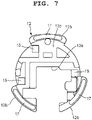
FIG. 7 is an enlarged rear view showing the inner surface side of the holder ofFIG. 6 ; -
FIG. 8 is an enlarged perspective view showing the undersurface side of a circuit board shown inFIG. 6 ; and -
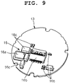
FIG. 9 is an enlarged perspective view showing the upper surface side of the circuit board shown inFIG. 6 . - An embodiment where the present invention has been applied in a body-worn device will hereinafter be described with reference to
FIG. 1 to FIG. 9 . - This body-worn device is a wristwatch type device that is used with it being worn on an arm, and includes a case 1, as shown in
FIG. 1 . To outer circumferential portions of the case 1 on the twelve o'clock side and the six o'clock side,bands 2 are attached so that the case 1 can be worn on a part of a body such as an arm. - Also, on outer circumferential portions of the case 1 which do not correspond to the
bands 2,push button switches 3 are provided, as shown inFIG. 1 . In addition, to the upper opening of the case 1, aglass 4 is attached. Moreover, to the lower part of the case 1, aback cover 5 that is an exterior member is attached by a plurality ofscrews 5b, as shown inFIG. 2 . - Also, inside the case 1, a module (not shown) is provided. This module includes various types of components, such as a display section for displaying biological information such as a pulse and various types of information regarding a time of day, a date, a day of the week, and the like, and a circuit section for electrically controlling the display section.
- On the inner surface of the
back cover 5, anelectrode plate 6, acushion member 7, and an insulation sheet (not shown) are provided, as shown inFIG. 3 . Theelectrode plate 6 has a substantially quadrilateral frame shape, and is attached to the inner surface of theback cover 5 by screws. On theelectrode plate 6, a plurality ofcontact pieces 6a is provided. As a result, theelectrode plate 6 is structured such that, when theback cover 5 is attached to the lower part of the case 1, the plurality ofcontact pieces 6a comes in contact with the circuit section of the module in the case 1. - The
cushion member 7 is structured to be provided on a portion of the inner surface of theback cover 5 and positioned outside the frame part of theelectrode plate 6, and to elastically hold down the module in the case 1 when theback cover 5 is attached to the lower part of the case 1, as shown inFIG. 3 andFIG. 4 . Although not shown in the drawings, the insulation sheet, which insulates adetection device 10 described later, is provided on a portion of the inner surface of theback cover 5 in a manner to be positioned in an area inside the frame part of theelectrode plate 6 excluding areas corresponding toelectronic components 16 of a later-describedcircuit board 13 of thedetection device 10, and covers thedetection device 10. - In the center area of the undersurface of the
back cover 5, aprojection section 8 having a substantially circular disk shape is provided, as shown inFIG. 2 . Thisprojection section 8 is structured to be pressed onto the skin of an arm when the case 1 is worn on the arm with thebands 2. In the inner surface of theprojection section 8, anarrangement recess section 9 is provided in which thedetection device 10 is arranged, as shown inFIG. 3 to FIG. 6 . - The
detection device 10 is configured to detect biological information such as a pulse with the case 1 being worn on an arm by thebands 2, as shown inFIG. 1 andFIG. 2 . More specifically, thedetection device 10 includes aprotective glass 11 which is a light transmissive transparent section and provided on theprojection section 8 of theback cover 5, and aholder 12 which is attached to thearrangement recess section 9 of theback cover 5 in a manner to be positioned opposing theprotective glass 11, as shown inFIG. 4 andFIG. 5 . - This
detection device 10 also includes thecircuit board 13 which is arranged between theholder 12 and the bottom of the arrangement recesssection 9 of theback cover 5, anoptical sensor 14 which is provided on one surface of thecircuit board 13 opposing theprotective glass 11, that is, the undersurface of thecircuit board 13 and detects light of a specific wavelength, and energizingmembers 15 which are arranged between theholder 12 and thecircuit board 13 and force thecircuit board 13 and theoptical sensor 14 toward theprotective glass 11, as shown inFIG. 4 andFIG. 5 . - The
protective glass 11 is fitted from below into anattachment recess section 8a in theprojection section 8 of theback cover 5 via awaterproof packing 11a, as shown inFIG. 4 andFIG. 5 . Here, thisprotective glass 11 is attached to the inner surface of theattachment recess section 8a, or more specifically, the ceiling surface of theattachment recess section 8a with a first two-sidedadhesive tape 11b. As a result, thisprotective glass 11 is structured to be pressed onto the skin of an arm together with theprojection section 8 of theback cover 5 when the case 1 is worn on the arm by thebands 2. - In this embodiment, in an area between the
attachment recess section 8a of theprojection section 8 and the arrangement recesssections 9 of theback cover 5, athrough hole 5a which connects these sections is provided, as shown inFIG. 4 andFIG. 5 . Accordingly, the first two-sidedadhesive tape 11b is formed in a substantially ring shape whose inner diameter is greater than that of thethrough hole 5a. That is, this first two-sidedadhesive tape 11b is structured to be provided on the ceiling surface of theattachment recess section 8a and positioned around the outer circumference of the throughhole 5a so that thethrough hole 5a is not closed. - The
circuit board 13 has a substantially circular plate shape and is made of a hard synthetic resin such as epoxy resin or glass epoxy resin, as shown inFIG. 4 andFIG. 5 . On the undersurface (the surface shown inFIG. 8 ) of thecircuit board 13, that is, on the back surface of thecircuit board 13, theoptical sensor 14 is provided, as shown inFIG. 8 . Also, on the upper surface (the surface shown inFIG. 9 ) of thecircuit board 13, that is, on the front surface of thecircuit board 13, the various types ofelectronic components 16 are provided, as shown inFIG. 9 . - These various types of
electronic components 16 includes an Integrated Circuit (IC)chip 16a which electrically controls theoptical sensor 14, aconnector 16b to which a flexible wiring substrate (not shown) is connected, and otherplural components 16c which are necessary for thedetection device 10 to detect biological information, as shown inFIG. 9 . - The
optical sensor 14 and the various types ofelectronic components 16 described above are attached and electrically connected to a plurality ofcircuit patterns 13a on the upper surface and undersurface of thecircuit board 13 by soldering, as shown inFIG. 4 andFIG. 5 . This plurality ofcircuit patterns 13a, that is, thecircuit pattern 13a on the upper surface and thecircuit pattern 13a on the undersurface are electrically connected by a plurality of through holes (not shown) provided in thecircuit board 13. - The
circuit board 13 is structured such that the flexible wiring substrate (not shown) is connected to theconnector 16b of theelectronic components 16 in the state shown inFIG. 3 , and electrically connected to the circuit section of the module in the case 1 through connection holes in the insulation sheet (not shown). - The
optical sensor 14, which detects pulses, has a substantially quadrangular plate shape and is provided on a substantially center portion of the undersurface (the surface shown inFIG. 8 ) of thecircuit board 13, as shown inFIG. 8 . Thisoptical sensor 14 is structured such that it is arranged in the throughhole 5a between theattachment recess section 8a of theprojection section 8 of theback cover 5 and the arrangement recesssection 9 of theback cover 5 and its undersurface comes in close contact with the upper surface of theprotective glass 11, as shown inFIG. 4 andFIG. 5 . - That is, the
optical sensor 14 is formed such that its thickness is greater than the axial length (depth) of the throughhole 5a, as shown inFIG. 4 andFIG. 5 . As a result, when theoptical sensor 14 is arranged in thethrough hole 5a with it being attached to the undersurface of thecircuit board 13, the lower part of theoptical sensor 14 projects under thethrough hole 5a. Accordingly, when the upper surface of theprotective glass 11 is pressed against the undersurface of theoptical sensor 14, thecircuit board 13 is pressed upward from the bottom of the arrangement recesssection 9. - Also, the
optical sensor 14 has alight emitting area 14a and alight receiving area 14b, as shown inFIG. 8 . Thelight emitting area 14a, which includes a light emitting element such as a Light Emitting Diode (LED), is structured to emit light of a specific wavelength, such as light of the green wavelength. Thelight receiving area 14b, which includes a light receiving element such as a Photo Diode (PD), is structured to receive reflected light derived by light from thelight emitting area 14a being applied to and reflecting on an arm, and convert the reflected light into an electric signal. - That is, the
optical sensor 14 is structured such that, when light of a specific wavelength is emitted from thelight emitting area 14a ofFIG. 8 to an arm with the case 1 ofFIG. 2 being worn on the arm by thebands 2, part of the emitted light is absorbed into blood in blood vessels, and the remaining light is reflected on the arm and received by thelight receiving area 14b. - Here, the amount of blood in the blood vessels varies every time the heart beats, and therefore the amount of reflected light resulting from the emitted light varies in accordance with the variation in the amount of blood. The above-described
optical sensor 14 is structured to receive a varied amount of reflected light by thelight receiving area 14b shown inFIG. 8 , convert it into an electric signal, and thereby detect a pulse. - On the other hand, the
holder 12 has a substantially circular plate shape and is made of a hard synthetic resin, as shown inFIG. 3 to FIG. 7 . Thisholder 12 is formed such that its thickness is sufficiently greater than the thickness of thecircuit board 13 and substantially equal to the depth of thearrangement recess section 9 formed in the inner surface of theback cover 5. Also, thisholder 12 is structured such that it is provided with aboard housing section 12c where thecircuit board 13 is arranged, and thecircuit board 13 is arranged in thisboard housing section 12c without protruding downward. - Outer
circumferential portions 12b of thisholder 12 downwardly project lower than thecircuit board 13, and the undersurfaces of these projecting outercircumferential portions 12b are attached to the bottom of thearrangement recess section 9 of theback cover 5 with second two-sidedadhesive tapes 17, whereby theholder 12 is fixed in thearrangement recess section 9 of theback cover 5, as shown inFIG. 4 to FIG. 7 . In this embodiment, the second two-sidedadhesive tapes 17 are applied to plural undersurface areas of the outercircumferential portions 12b of theholder 12, or more specifically, three areas including an area between the eleven o'clock side and the one o'clock side, an area between the three o'clock side and the five o'clock side, and an area between the seven o'clock side and the nine o'clock side, as shown inFIG. 7 . - Also, this
holder 12 is provided with anopening section 12a corresponding to theoptical sensor 14 and the various types ofelectronic components 16 provided on thecircuit board 13, as shown inFIG. 4 to FIG. 7 . More specifically, theopening section 12a is a substantially quadrangular hole formed by part of theholder 12 from its substantially center portion to its outer circumferential rim portion on the six o' clock side being cut out. - As a result of this structure, when the
holder 12 is attached to the bottom of thearrangement recess section 9 of theback cover 5 with thecircuit board 13 being arranged in theboard housing section 12c in theholder 12, the various types ofelectronic components 16 provided on the upper surface of thecircuit board 13 are arranged in theopening section 12a of theholder 12, and theoptical sensor 14 provided on the undersurface of thecircuit board 13 is arranged corresponding to theopening section 12a of theholder 12, as shown inFIG. 3 to FIG. 7 . - The energizing
members 15 are made of cushioning material, as shown inFIG. 4 andFIG. 7 . However, they may be spring members such as coil springs or plate springs. Each of the energizingmembers 15 is structured to force thecircuit board 13 toward theprotective glass 11, that is, the bottom of thearrangement recess section 9 of theback cover 5. These energizingmembers 15 are arranged in compressed states in areas between the undersurface of theholder 12 and the upper surface of thecircuit board 13 while avoiding an area corresponding to theoptical sensor 14 and the various types ofelectronic components 16 provided on thecircuit board 13. - That is, on the inner surface of the
board housing section 12c of theholder 12, these energizingmembers 15 are provided in a plurality of areas, or more specifically, three areas that are located around the outer periphery of theopening section 12a on a substantially three o'clock side, a substantially nine o'clock side, and a substantially eleven o'clock side, and do not include areas corresponding to the second two-sidedadhesive tapes 17 on theholder 12 and the area corresponding to theoptical sensor 14 and the various types ofelectronic components 16 provided on thecircuit board 13, as shown inFIG. 7 . - As a result of this structure, while being compressed by the
holder 12 fixed in thearrangement recess section 9 of theback cover 5, the energizingmembers 15 force thecircuit board 13 toward the bottom of thearrangement recess section 9 of theback cover 5 such that thecircuit board 13 is evenly pressed with balance, and thereby press the undersurface of theoptical sensor 14 on thecircuit board 13 against the upper surface of theprotective glass 11 such that the undersurface of theoptical sensor 14 is evenly pressed with balance and comes in close contact with the upper surface of theprotective glass 11, as shown inFIG. 4 andFIG. 7 . In this embodiment, the fitting force of theprotective glass 11 with respect to theattachment recess section 8a of theback cover 5 is greater than the energizing force of the energizingmembers 15. - As a result, the
circuit board 13 is structured to be held between theprotective glass 11 and theholder 12 when the undersurface of theoptical sensor 14 is pressed against the upper surface of theprotective glass 11 by the energizing force of the energizingmembers 15 in the compressed states, and thereby arranged in a floating state in thearrangement recess section 9 without coming in contact with the bottom surface of thearrangement recess section 9 and the inner surface of theboard housing section 12c of theholder 12, as shown inFIG. 4 . - Here, since the thickness of the
optical sensor 14 in a vertical direction is greater than the axial length (depth) of the throughhole 5a provided between theattachment recess section 8a in theprojection section 8 of theback cover 5 and thearrangement recess section 9 of theback cover 5, the lower part of theoptical sensor 14 downwardly protrudes from the throughhole 5a when theoptical sensor 14 is inserted into the throughhole 5a, as shown inFIG. 4 andFIG. 5 . As a result of this structure, the undersurface of theoptical sensor 14 is pressed by the upper surface of theprotective glass 11, whereby thecircuit board 13 is pressed above the bottom of thearrangement recess section 9. - As a result, the
circuit board 13 is structured to be held between theprotective glass 11 and theholder 12 and arranged in the floating state in theboard housing section 12c of theholder 12 in thearrangement recess section 9 without its undersurface coming in contact with the bottom surface of thearrangement recess section 9 and its upper surface coming in contact with the inner surface of theboard housing section 12c of theholder 12, as shown inFIG. 4 . - Next, the mechanism of this body-worn device is described.
- When this body-worn device is to be used, first, the case 1 is worn on an arm by the
bands 2 with theback cover 5 of the case 1 being arranged on the arm. Here, theprojection section 8 of theback cover 5 is pressed against and comes in close contact with the skin of the arm with theprotective glass 11 on theprojection section 8 being pressed onto the skin. - In this state, one of the plurality of push button switches 3 on the case 1 is operated to switch the current mode to a pulse detection mode, whereby the
detection device 10 provided in theback cover 5 starts pulse detection. In this detection, light of a specific wavelength, such as light of the green wavelength, is emitted from thelight emitting area 14a of theoptical sensor 14 of thedetection device 10, and applied to the skin of the arm through theprotective glass 11. - Here, since the
protective glass 11 has been pressed onto and is in close contact with the skin of the arm, external light from outside the case 1 is blocked and only the light of the specific wavelength from thelight emitting area 14a is applied to the skin of the arm. Part of this applied light is absorbed into blood in blood vessels under the skin and the remaining light is reflected. This reflected light is received by thelight receiving area 14b of theoptical sensor 14 through theprotective glass 11 and converted into an electrical signal. - Here, blood in the blood vessels flows with pulses. Accordingly, the amount of blood therein varies every time the heart beats. Thus, the amount of reflected light resulting from the emitted light of the specific wavelength varies in accordance with the variation in the amount of blood, and a varied amount of reflected light is received by the
light receiving area 14b of theoptical sensor 14 through theprotective glass 11. This light received by thelight receiving area 14b is converted into an electrical signal, and a pulse is measured by an integrated circuit chip 15a of theelectronic components 16 on thecircuit board 13 on the basis of the electrical signal. - Also, here, the
circuit board 13 has been forced toward theprotective glass 11 by the energizingmembers 15 in the compressed states, and the undersurface of theoptical sensor 14 provided on thecircuit board 13 is in close contact with the upper surface ofprotective glass 11. Accordingly, in the pulse detection by thedetection device 10, the light of the specific wavelength emitted from thelight emitting area 14a of theoptical sensor 14 is prevented from being reflected on the upper surface of theprotective glass 11. That is, light reflection thereon can be suppressed. - More specifically, if the light of the specific wavelength emitted from the
light emitting area 14a is reflected on the upper surface of theprotective glass 11, this reflected light is received by thelight receiving area 14b as noise, or in other words, as light other than that reflected on the skin of the arm. By this light reflection on the upper surface of theprotective glass 11 being suppressed, the light emitted from thelight emitting area 14a can be efficiently applied to the skin of the arm through theprotective glass 11, which enhances the detection performance. - In this
detection device 10, when the undersurface of theoptical sensor 14 is pressed against the upper surface of theprotective glass 11 by the energizing force of the energizingmembers 15, thecircuit board 13 is held between theprotective glass 11 and theholder 12 and thereby arranged in the floating state in thearrangement recess section 9 without coming in contact with the bottom surface of thearrangement recess section 9 and the inner surface of theboard housing section 12c of theholder 12. - As a result of this structure, in this
detection device 10, theoptical sensor 14 provided on thecircuit board 13 is evenly pressed against theprotective glass 11 with balance by the energizing force of the energizingmembers 15. In addition, in the case of thisdetection device 10, when the case 1 is subjected to an external impact, this impact is buffered by the energizingmembers 15, and therefore thecircuit board 13 is not affected by the impact. By this structure as well, the detection performance of thedetection device 10 is enhanced. - In
Japanese Patent Application Laid-Open (Kokai) Publication No. 2005-270543 - This detection device disclosed in
Japanese Patent Application Laid-Open (Kokai) Publication No. 2005-270543 - However, this detection device has a problem in that, because of the structure where the flexible substrate is attached to the back cover and the optical sensor is positioned close to the protective glass by the resilience of the flexible substrate, the contact state of the optical sensor with respect to the protective glass is unstable, and therefore it is difficult to reliably and favorably bring the optical sensor into close contact with the protective glass.
- In contrast, the
detection device 10 in the body-worn device of the present embodiment includes theback cover 5 which is an exterior member and having theprotective glass 11 that is a light transmissive transparent section, theholder 12 which is attached to theback cover 5 in a manner to be positioned opposing theprotective glass 11, thecircuit board 13 which is arranged between theback cover 5 and theholder 12, theoptical sensor 14 which is provided on one surface of thecircuit board 13 opposing theprotective glass 11, that is, the undersurface of thecircuit board 13 and detects light of a specific wavelength, and the energizingmembers 15 which are arranged between theholder 12 and thecircuit board 13 and force thecircuit board 13 and theoptical sensor 14 toward theprotective glass 11, whereby theoptical sensor 14 can be favorably brought into close contact with theprotective glass 11. - More specifically, in this
detection device 10, thecircuit board 13 arranged between theback cover 5 and theholder 12 is forced toward theprotective glass 11 by the energizingmembers 15 and, by the energizing force of these energizingmembers 15, presses theoptical sensor 14 against theprotective glass 11. As a result of this structure, theoptical sensor 14 can be reliably and favorably brought into close contact with theprotective glass 11 in a stable state. - In this
detection device 10 of the present embodiment, theoptical sensor 14 includes thelight emitting area 14a and thelight receiving area 14b. Light emitted from thelight emitting area 14a is applied to a part of a body such as an arm, and reflected light resulting from this applied light is received by thelight receiving area 14b, whereby biological information such as a pulse is detected. - More specifically, in the case of this
detection device 10, light of a specific wavelength, such as light of the green wavelength, is emitted from thelight emitting area 14a of theoptical sensor 14 and applied to the skin of an arm. Part of this emitted light is absorbed into blood in blood vessels under the skin, and the remaining light is reflected, received by thelight receiving area 14b of theoptical sensor 14, and converted into an electric signal, whereby a pulse is detected. - Here, blood in the blood vessels flows with pulses. Accordingly, the amount of blood therein varies every time the heart beats . Thus, the amount of reflected light resulting from the emitted light of the specific wavelength varies in accordance with the variation in the amount of blood, and a varied amount of reflected light is received by the
light receiving area 14b of theoptical sensor 14 in thedetection device 10. This reflected light received by thelight receiving area 14b is converted into an electrical signal, and a pulse is measured by the integrated circuit chip 15a of theelectronic components 16 on thecircuit board 13 on the basis of the electrical signal. - Also, in this
detection device 10, theoptical sensor 14 is pressed against theprotective glass 11 by the energizing force of the energizingmembers 15 forcing thecircuit board 13, whereby theoptical sensor 14 is reliably and favorably brought into close contact with theprotective glass 11 in the stable state. Accordingly, in thisdetection device 10, light reflection on the upper surface of theprotective glass 11 when light emitted by theoptical sensor 14 passes through theprotective glass 11, that is, reflected light to be taken as noise can be suppressed, which enhances the detection performance. - That is, in this
detection device 10, since the undersurface of theoptical sensor 14 is in close contact with the upper surface of theprotective glass 11, light reflection on the upper surface of theprotective glass 11 when light emitted by thelight emitting area 14a of theoptical sensor 14 passes through theprotective glass 11, that is, reflected light to be taken as noise is suppressed, whereby the light emitted by thelight emitting area 14a efficiently passes through theprotective glass 11 and is favorably applied to the skin of an arm. - As a result of this structure, in this
detection device 10, a situation can be prevented in which, when light reflected on a part of a body such as an arm after passing through theprotective glass 11 is to be received by theoptical sensor 14, light reflected on the upper surface of theprotective glass 11 and existing as noise, that is, light other than that reflected on the skin of the arm is received. Thus, the detection performance of thedetection device 10 is further enhanced. - Also, in this
detection device 10, thecircuit board 13 is arranged in the floating state where it is not in contact with theback cover 5 that is an exterior member and theholder 12. As a result of this structure, theoptical sensor 14 provided on thecircuit board 13 is evenly pressed against theprotective glass 11 with balance by the energizing force of the energizingmembers 15. In addition, when the case 1 is subjected to an external impact, this impact is buffered by the energizingmembers 15, so that thecircuit board 13 can be prevented from being affected by the impact. By this structure as well, the detection performance of thedetection device 10 is enhanced. - That is, in this
detection device 10, thecircuit board 13 held between theprotective glass 11 and theholder 12 with the undersurface of theoptical sensor 14 being pressed against the upper surface of theprotective glass 11 by the energizing force of the energizingmembers 15 is in the floating state in thearrangement recess section 9 without being in contact with the bottom surface of thearrangement recess section 9 and the inner surface of theboard housing section 12c of theholder 12. - As a result of this structure, in this
detection device 10, theoptical sensor 14 provided on thecircuit board 13 is evenly pressed against theprotective glass 11 with balance by the energizing force of the energizingmembers 15 and, even if the case 1 is subjected to an external impact, this impact is buffered by the energizingmembers 15, so that thecircuit board 13 can be prevented from being affected by the impact. - Also, in the case of this
detection device 10, the energizingmembers 15 are made of cushioning material, and arranged on outer circumferential areas on the other surface of thecircuit board 13, that is, the upper surface of thecircuit board 13 while avoiding the area corresponding to theoptical sensor 14. As a result of this structure, a portion of thecircuit board 13 corresponding to theoptical sensor 14 is not pressed when the energizingmembers 15 force thecircuit board 13, whereby thecircuit board 13 can be favorably pressed by the energizing force of the energizingmembers 15 and theoptical sensor 14 can be favorably pressed against theprotective glass 11. - That is, in this
detection device 10, the energizingmembers 15 are arranged on the plurality of outer circumferential areas on the upper surface of thecircuit board 13, or more specifically, three areas on a substantially three o'clock side, a substantially nine o'clock side, and a substantially eleven o'clock side, whereby thecircuit board 13 excluding its portion corresponding to theoptical sensor 14 and the various types ofelectronic components 16 provided on thecircuit board 13 is evenly pressed with balance by the energizing force of the energizingmembers 15. As a result of this structure, theoptical sensor 14 can be further reliably and favorably brought into close contact with theprotective glass 11 in the stable state. - Here, in this
detection device 10, the energizingmembers 15 are arranged in the compressed states in the areas between theholder 12 and thecircuit board 13. As a result, by the energizing force of these energizingmembers 15, thecircuit board 13 is further evenly pressed with balance, whereby theoptical sensor 14 can be further reliably and favorably brought into close contact with theprotective glass 11 in the stable state. - Also, in this
detection device 10, theopening section 12a corresponding to theoptical sensor 14 is formed in theholder 12. By thisopening section 12a of theholder 12, the portion of thecircuit board 13 corresponding to theoptical sensor 14 is not pressed even when thecircuit board 13 is forced by the energizingmembers 15 arranged between theholder 12 and thecircuit board 13, whereby theoptical sensor 14 can be favorably arranged on theprotective glass 11 by the energizingmembers 15 without being affected by theholder 12. - In the case of this
detection device 10, in theopening section 12a, theelectronic components 16 provided on the other surface of thecircuit board 13, that is, the upper surface of thecircuit board 13 while avoiding the energizingmembers 15 is arranged. As a result of this structure, when thecircuit board 13 is arranged in theholder 12, theelectronic components 16 of thecircuit board 13 are arranged in theopening section 12a of theholder 12, and thereby can be prevented from coming in contact with theholder 12. - In the above-described embodiment, as the transparent section which is light transmissive, the
protective glass 11 is used. However, the present invention is not limited thereto, and a light transmissive plate made of a synthetic resin, such as Polymethyl methacrylate (PMMA) or Polycarbonate (PC), may be adopted. Also, for example, a transparent material provided with a film through which light of a specific wavelength passes or a filter layer such as an evaporated film may be adopted as the transparent section. - Also, in the above-described embodiment, the energizing
members 15 are arranged on the plurality of outer circumferential areas on the upper surface of thecircuit board 13. However, the present invention is not limited thereto, and the energizingmembers 15 may be arranged on any portion of the upper surface of thecircuit board 13 as long as it is not a portion corresponding to theoptical sensor 14 and the various types ofelectronic components 16 mounted on thecircuit board 13. - Moreover, in the above-described embodiment, the energizing
members 15 are made of cushioning material. However, the present invention is not limited thereto, and spring members such as extension coil springs may serve as the energizingmembers 15. In that case, a structure in which theprotective glass 11 that is a transparent section is pulled toward theoptical sensor 14 side, a structure in which thecircuit board 13 and theoptical sensor 14 are pulled toward theprotective glass 11, or a structure in which theholder 12 is pulled toward thecircuit board 13 may be adopted. - Furthermore, in the above-described embodiment, the undersurfaces of the outer
circumferential portions 12b of theholder 12 are attached to the bottom of thearrangement recess section 9 of theback cover 5 with the second two-sidedadhesive tapes 17. However, the present invention is not limited thereto, and a structure may be adopted in which theholder 12 is attached to thearrangement recess section 9 of theback cover 5 with fastening members such as screw members. - Still further, in the above-described embodiment, the body-worn device is worn on an arm and used. However, the present invention is not limited thereto, and it may be worn on a part of a body other than arms.
Claims (10)
- A detection device (10) comprising:an exterior member (5) which is provided with a light transmissive transparent portion (11);a holder (12) which is attached to the exterior member (5) and positioned opposing the transparent portion (11);a circuit board (13) which is arranged between the exterior member (5) and the holder (12);an optical sensor (14) which is provided on one surface of the circuit board (13) opposing the transparent portion (11) to detect light; andan energizing member (15) which is arranged between the holder (12) and the circuit board (13), and forces the circuit board (13) and the optical sensor (14) toward the transparent portion (11).
- The detection device (10) according to claim 1, wherein the optical sensor (14) has a light emitting area (14a) and a light receiving area (14b).
- The detection device (10) according to claim 1 or 2, wherein the optical sensor (14) is pressed against the transparent portion (11) by energizing force of the energizing member (15) forcing the circuit board (13).
- The detection device (10) according to any one of claims 1 to 3, wherein the circuit board (13) is arranged in a floating state where the circuit board (13) is not in contact with the exterior member (5) and the holder (12).
- The detection device (10) according to any one of claims 1 to 4, wherein the energizing member (15) is made of cushioning material, and arranged on an outer circumferential area which is on an other surface opposite to the one surface of the circuit board (13) and does not include an area corresponding the optical sensor (14).
- The detection device (10) according to claim 5, wherein the energizing member (15) is in a compressed state when arranged between the holder (12) and the circuit board (13).
- The detection device (10) according to any one of claims 1 to 6, wherein the holder (12) has an opening portion (12a) provided corresponding to the optical sensor (14).
- The detection device (10) according to claim 7, wherein an electronic component (16) provided on an other surface of the circuit board (13) while avoiding the energizing member (15) is arranged in the opening portion (12a).
- The detection device (10) according to any one of claims 1 to 8, wherein light of a specific wavelength passes through the transparent portion (11).
- A body-worn device comprising the detection device (10) according to any one of claims 1 to 9.
Applications Claiming Priority (2)
| Application Number | Priority Date | Filing Date | Title |
|---|---|---|---|
| JP2020200944 | 2020-12-03 | ||
| JP2021051244A JP7242007B2 (en) | 2020-12-03 | 2021-03-25 | Sensing devices and body-worn devices |
Publications (2)
| Publication Number | Publication Date |
|---|---|
| EP4009120A1 true EP4009120A1 (en) | 2022-06-08 |
| EP4009120B1 EP4009120B1 (en) | 2026-02-25 |
Family
ID=78819343
Family Applications (1)
| Application Number | Title | Priority Date | Filing Date |
|---|---|---|---|
| EP21211012.6A Active EP4009120B1 (en) | 2020-12-03 | 2021-11-29 | Detection device and body-worn device |
Country Status (3)
| Country | Link |
|---|---|
| US (2) | US20220175262A1 (en) |
| EP (1) | EP4009120B1 (en) |
| CN (1) | CN114587270B (en) |
Citations (4)
| Publication number | Priority date | Publication date | Assignee | Title |
|---|---|---|---|---|
| JP2005270543A (en) | 2004-03-26 | 2005-10-06 | Seiko Instruments Inc | Biological information measuring device |
| US20070191718A1 (en) * | 2006-02-16 | 2007-08-16 | Hisao Nakamura | Pulse measuring apparatus |
| US20180348048A1 (en) * | 2014-04-07 | 2018-12-06 | PAI Health Inc. | Systems and Methods for Monitoring Physiological Parameters |
| US20190082985A1 (en) * | 2012-06-22 | 2019-03-21 | Fitbit, Inc. | Optical device for determining pulse rate |
Family Cites Families (14)
| Publication number | Priority date | Publication date | Assignee | Title |
|---|---|---|---|---|
| US5249576A (en) * | 1991-10-24 | 1993-10-05 | Boc Health Care, Inc. | Universal pulse oximeter probe |
| US20110054277A1 (en) * | 2008-05-09 | 2011-03-03 | Koninklijke Philips Electronics N.V. | Contactless respiration monitoring of a patient and optical sensor for a photoplethysmography measurement |
| JP6251997B2 (en) * | 2012-09-18 | 2017-12-27 | カシオ計算機株式会社 | Pulse data detection device, pulse data detection method, and pulse data detection program |
| JP5880535B2 (en) * | 2013-12-25 | 2016-03-09 | セイコーエプソン株式会社 | Biological information detection device |
| US9980657B2 (en) * | 2014-05-30 | 2018-05-29 | Microsoft Technology Licensing, Llc | Data recovery for optical heart rate sensors |
| JP2016047086A (en) * | 2014-08-27 | 2016-04-07 | セイコーエプソン株式会社 | Biological information detection device |
| US9696199B2 (en) * | 2015-02-13 | 2017-07-04 | Taiwan Biophotonic Corporation | Optical sensor |
| JP6627374B2 (en) * | 2015-02-17 | 2020-01-08 | カシオ計算機株式会社 | Electronics |
| US10485437B2 (en) * | 2015-03-30 | 2019-11-26 | Bose Corporation | Light guide system for physiological sensor |
| CN206877213U (en) * | 2017-06-05 | 2018-01-12 | 惠州Tcl移动通信有限公司 | Possesses the wearable device of heart rate detecting function |
| TWM561502U (en) * | 2017-12-13 | 2018-06-11 | 正崴精密工業股份有限公司 | Device for measuring human physiological signal |
| FI128165B (en) * | 2018-05-18 | 2019-11-29 | Corle Oy | Body sensor |
| US11158757B2 (en) * | 2018-11-27 | 2021-10-26 | Epistar Corporation | Optical sensing device and optical sensing system thereof comprising a light receiving device capable of receiving a first received wavelength having a largest external quantum efficiency |
| US11213213B2 (en) * | 2019-03-26 | 2022-01-04 | Kotl, Llc | Systems and methods of combined optical coherence tomography and pressure measurement |
-
2021
- 2021-11-29 EP EP21211012.6A patent/EP4009120B1/en active Active
- 2021-12-02 CN CN202111458837.7A patent/CN114587270B/en active Active
- 2021-12-03 US US17/541,887 patent/US20220175262A1/en active Pending
-
2024
- 2024-07-23 US US18/780,914 patent/US20240374156A1/en active Pending
Patent Citations (4)
| Publication number | Priority date | Publication date | Assignee | Title |
|---|---|---|---|---|
| JP2005270543A (en) | 2004-03-26 | 2005-10-06 | Seiko Instruments Inc | Biological information measuring device |
| US20070191718A1 (en) * | 2006-02-16 | 2007-08-16 | Hisao Nakamura | Pulse measuring apparatus |
| US20190082985A1 (en) * | 2012-06-22 | 2019-03-21 | Fitbit, Inc. | Optical device for determining pulse rate |
| US20180348048A1 (en) * | 2014-04-07 | 2018-12-06 | PAI Health Inc. | Systems and Methods for Monitoring Physiological Parameters |
Also Published As
| Publication number | Publication date |
|---|---|
| EP4009120B1 (en) | 2026-02-25 |
| CN114587270B (en) | 2026-01-09 |
| US20240374156A1 (en) | 2024-11-14 |
| CN114587270A (en) | 2022-06-07 |
| US20220175262A1 (en) | 2022-06-09 |
Similar Documents
| Publication | Publication Date | Title |
|---|---|---|
| US5520177A (en) | Oximeter probe | |
| US8787120B2 (en) | Exterior element for a wristwatch | |
| CN109061946B (en) | Display components and electronic equipment | |
| CN100511530C (en) | Keyboard with key supporting structure for portable electronic devices | |
| US20180000362A1 (en) | Biological information measuring module and biological information measuring apparatus | |
| CA2485762A1 (en) | Multi-mode electromagnetic radiaton emitting device | |
| EP4009120B1 (en) | Detection device and body-worn device | |
| JP7242007B2 (en) | Sensing devices and body-worn devices | |
| JP2514414B2 (en) | Light emitting element resin sealing structure for printed circuit board | |
| US20240423492A1 (en) | Detection device and timepiece | |
| CN101609354B (en) | Electronic equipment | |
| JPH09318774A (en) | Sound generator | |
| JP2006292833A (en) | Electronics | |
| CN209996311U (en) | human physiological parameter monitoring components and wearing equipment | |
| JP4655112B2 (en) | Electronic equipment and electronic components | |
| CN110365817B (en) | Housing assembly and mobile terminal | |
| JP2010161020A (en) | Operating input device and electronic device using the same | |
| CN210784285U (en) | Casing, health monitoring device and wearable equipment | |
| CN223054289U (en) | Tea bar machine and operation panel assembly thereof | |
| US12607967B2 (en) | Sensor device and timepiece | |
| HK40096172A (en) | Detection device and timepiece | |
| JP2014181923A (en) | Electronic apparatus | |
| JP6531493B2 (en) | Electronics | |
| JP7494869B2 (en) | Detection devices and clocks | |
| JPH07218913A (en) | Liquid crystal display device with backlight |
Legal Events
| Date | Code | Title | Description |
|---|---|---|---|
| PUAI | Public reference made under article 153(3) epc to a published international application that has entered the european phase |
Free format text: ORIGINAL CODE: 0009012 |
|
| STAA | Information on the status of an ep patent application or granted ep patent |
Free format text: STATUS: REQUEST FOR EXAMINATION WAS MADE |
|
| 17P | Request for examination filed |
Effective date: 20211129 |
|
| AK | Designated contracting states |
Kind code of ref document: A1 Designated state(s): AL AT BE BG CH CY CZ DE DK EE ES FI FR GB GR HR HU IE IS IT LI LT LU LV MC MK MT NL NO PL PT RO RS SE SI SK SM TR |
|
| RBV | Designated contracting states (corrected) |
Designated state(s): AL AT BE BG CH CY CZ DE DK EE ES FI FR GB GR HR HU IE IS IT LI LT LU LV MC MK MT NL NO PL PT RO RS SE SI SK SM TR |
|
| STAA | Information on the status of an ep patent application or granted ep patent |
Free format text: STATUS: EXAMINATION IS IN PROGRESS |
|
| 17Q | First examination report despatched |
Effective date: 20240417 |
|
| REG | Reference to a national code |
Ref country code: DE Ref legal event code: R079 Ipc: G04G0017040000 Ref country code: DE Ref legal event code: R079 Ref document number: 602021048588 Country of ref document: DE Free format text: PREVIOUS MAIN CLASS: G04G0021020000 Ipc: G04G0017040000 |
|
| RIC1 | Information provided on ipc code assigned before grant |
Ipc: G04G 17/04 20060101AFI20250828BHEP Ipc: G04G 21/02 20100101ALI20250828BHEP |
|
| GRAP | Despatch of communication of intention to grant a patent |
Free format text: ORIGINAL CODE: EPIDOSNIGR1 |
|
| STAA | Information on the status of an ep patent application or granted ep patent |
Free format text: STATUS: GRANT OF PATENT IS INTENDED |
|
| INTG | Intention to grant announced |
Effective date: 20251007 |
|
| GRAS | Grant fee paid |
Free format text: ORIGINAL CODE: EPIDOSNIGR3 |
|
| GRAA | (expected) grant |
Free format text: ORIGINAL CODE: 0009210 |
|
| STAA | Information on the status of an ep patent application or granted ep patent |
Free format text: STATUS: THE PATENT HAS BEEN GRANTED |
|
| AK | Designated contracting states |
Kind code of ref document: B1 Designated state(s): AL AT BE BG CH CY CZ DE DK EE ES FI FR GB GR HR HU IE IS IT LI LT LU LV MC MK MT NL NO PL PT RO RS SE SI SK SM TR |
|
| REG | Reference to a national code |
Ref country code: CH Ref legal event code: F10 Free format text: ST27 STATUS EVENT CODE: U-0-0-F10-F00 (AS PROVIDED BY THE NATIONAL OFFICE) Effective date: 20260225 Ref country code: GB Ref legal event code: FG4D |
|
| REG | Reference to a national code |
Ref country code: DE Ref legal event code: R096 Ref document number: 602021048588 Country of ref document: DE |
|
| REG | Reference to a national code |
Ref country code: IE Ref legal event code: FG4D |
|
| REG | Reference to a national code |
Ref country code: NL Ref legal event code: MP Effective date: 20260225 |
|
| PG25 | Lapsed in a contracting state [announced via postgrant information from national office to epo] |
Ref country code: RS Free format text: LAPSE BECAUSE OF FAILURE TO SUBMIT A TRANSLATION OF THE DESCRIPTION OR TO PAY THE FEE WITHIN THE PRESCRIBED TIME-LIMIT Effective date: 20260525 |
|
| PG25 | Lapsed in a contracting state [announced via postgrant information from national office to epo] |
Ref country code: ES Free format text: LAPSE BECAUSE OF FAILURE TO SUBMIT A TRANSLATION OF THE DESCRIPTION OR TO PAY THE FEE WITHIN THE PRESCRIBED TIME-LIMIT Effective date: 20260225 |
|
| PG25 | Lapsed in a contracting state [announced via postgrant information from national office to epo] |
Ref country code: PL Free format text: LAPSE BECAUSE OF FAILURE TO SUBMIT A TRANSLATION OF THE DESCRIPTION OR TO PAY THE FEE WITHIN THE PRESCRIBED TIME-LIMIT Effective date: 20260225 |
|
| PG25 | Lapsed in a contracting state [announced via postgrant information from national office to epo] |
Ref country code: GR Free format text: LAPSE BECAUSE OF FAILURE TO SUBMIT A TRANSLATION OF THE DESCRIPTION OR TO PAY THE FEE WITHIN THE PRESCRIBED TIME-LIMIT Effective date: 20260526 |
|
| REG | Reference to a national code |
Ref country code: LT Ref legal event code: MG9D |
|
| PG25 | Lapsed in a contracting state [announced via postgrant information from national office to epo] |
Ref country code: LT Free format text: LAPSE BECAUSE OF FAILURE TO SUBMIT A TRANSLATION OF THE DESCRIPTION OR TO PAY THE FEE WITHIN THE PRESCRIBED TIME-LIMIT Effective date: 20260225 |
|
| PG25 | Lapsed in a contracting state [announced via postgrant information from national office to epo] |
Ref country code: NO Free format text: LAPSE BECAUSE OF FAILURE TO SUBMIT A TRANSLATION OF THE DESCRIPTION OR TO PAY THE FEE WITHIN THE PRESCRIBED TIME-LIMIT Effective date: 20260525 |
|
| PG25 | Lapsed in a contracting state [announced via postgrant information from national office to epo] |
Ref country code: FI Free format text: LAPSE BECAUSE OF FAILURE TO SUBMIT A TRANSLATION OF THE DESCRIPTION OR TO PAY THE FEE WITHIN THE PRESCRIBED TIME-LIMIT Effective date: 20260225 Ref country code: AT Free format text: LAPSE BECAUSE OF FAILURE TO SUBMIT A TRANSLATION OF THE DESCRIPTION OR TO PAY THE FEE WITHIN THE PRESCRIBED TIME-LIMIT Effective date: 20260225 Ref country code: SE Free format text: LAPSE BECAUSE OF FAILURE TO SUBMIT A TRANSLATION OF THE DESCRIPTION OR TO PAY THE FEE WITHIN THE PRESCRIBED TIME-LIMIT Effective date: 20260225 |
|
| REG | Reference to a national code |
Ref country code: AT Ref legal event code: MK05 Ref document number: 1891533 Country of ref document: AT Kind code of ref document: T Effective date: 20260225 |
|
| PG25 | Lapsed in a contracting state [announced via postgrant information from national office to epo] |
Ref country code: HR Free format text: LAPSE BECAUSE OF FAILURE TO SUBMIT A TRANSLATION OF THE DESCRIPTION OR TO PAY THE FEE WITHIN THE PRESCRIBED TIME-LIMIT Effective date: 20260225 |
|
| PG25 | Lapsed in a contracting state [announced via postgrant information from national office to epo] |
Ref country code: IS Free format text: LAPSE BECAUSE OF FAILURE TO SUBMIT A TRANSLATION OF THE DESCRIPTION OR TO PAY THE FEE WITHIN THE PRESCRIBED TIME-LIMIT Effective date: 20260625 Ref country code: PT Free format text: LAPSE BECAUSE OF FAILURE TO SUBMIT A TRANSLATION OF THE DESCRIPTION OR TO PAY THE FEE WITHIN THE PRESCRIBED TIME-LIMIT Effective date: 20260625 |
|
| PG25 | Lapsed in a contracting state [announced via postgrant information from national office to epo] |
Ref country code: NL Free format text: LAPSE BECAUSE OF FAILURE TO SUBMIT A TRANSLATION OF THE DESCRIPTION OR TO PAY THE FEE WITHIN THE PRESCRIBED TIME-LIMIT Effective date: 20260225 |
|
| PG25 | Lapsed in a contracting state [announced via postgrant information from national office to epo] |
Ref country code: LV Free format text: LAPSE BECAUSE OF FAILURE TO SUBMIT A TRANSLATION OF THE DESCRIPTION OR TO PAY THE FEE WITHIN THE PRESCRIBED TIME-LIMIT Effective date: 20260225 |
|
| PG25 | Lapsed in a contracting state [announced via postgrant information from national office to epo] |
Ref country code: BG Free format text: LAPSE BECAUSE OF FAILURE TO SUBMIT A TRANSLATION OF THE DESCRIPTION OR TO PAY THE FEE WITHIN THE PRESCRIBED TIME-LIMIT Effective date: 20260225 |