EP4008758A2 - Organometallic compound, light-emitting device including organometallic compound, and electronic apparatus including light-emitting device - Google Patents
Organometallic compound, light-emitting device including organometallic compound, and electronic apparatus including light-emitting device Download PDFInfo
- Publication number
- EP4008758A2 EP4008758A2 EP21206644.3A EP21206644A EP4008758A2 EP 4008758 A2 EP4008758 A2 EP 4008758A2 EP 21206644 A EP21206644 A EP 21206644A EP 4008758 A2 EP4008758 A2 EP 4008758A2
- Authority
- EP
- European Patent Office
- Prior art keywords
- group
- substituted
- unsubstituted
- formula
- independently
- Prior art date
- Legal status (The legal status is an assumption and is not a legal conclusion. Google has not performed a legal analysis and makes no representation as to the accuracy of the status listed.)
- Granted
Links
Images


Classifications
-
- H—ELECTRICITY
- H10—SEMICONDUCTOR DEVICES; ELECTRIC SOLID-STATE DEVICES NOT OTHERWISE PROVIDED FOR
- H10K—ORGANIC ELECTRIC SOLID-STATE DEVICES
- H10K85/00—Organic materials used in the body or electrodes of devices covered by this subclass
- H10K85/30—Coordination compounds
- H10K85/341—Transition metal complexes, e.g. Ru(II)polypyridine complexes
- H10K85/346—Transition metal complexes, e.g. Ru(II)polypyridine complexes comprising platinum
-
- C—CHEMISTRY; METALLURGY
- C07—ORGANIC CHEMISTRY
- C07B—GENERAL METHODS OF ORGANIC CHEMISTRY; APPARATUS THEREFOR
- C07B59/00—Introduction of isotopes of elements into organic compounds ; Labelled organic compounds per se
-
- C—CHEMISTRY; METALLURGY
- C07—ORGANIC CHEMISTRY
- C07B—GENERAL METHODS OF ORGANIC CHEMISTRY; APPARATUS THEREFOR
- C07B59/00—Introduction of isotopes of elements into organic compounds ; Labelled organic compounds per se
- C07B59/004—Acyclic, carbocyclic or heterocyclic compounds containing elements other than carbon, hydrogen, halogen, oxygen, nitrogen, sulfur, selenium or tellurium
-
- C—CHEMISTRY; METALLURGY
- C07—ORGANIC CHEMISTRY
- C07F—ACYCLIC, CARBOCYCLIC OR HETEROCYCLIC COMPOUNDS CONTAINING ELEMENTS OTHER THAN CARBON, HYDROGEN, HALOGEN, OXYGEN, NITROGEN, SULFUR, SELENIUM OR TELLURIUM
- C07F15/00—Compounds containing elements of Groups 8, 9, 10 or 18 of the Periodic Table
- C07F15/0006—Compounds containing elements of Groups 8, 9, 10 or 18 of the Periodic Table compounds of the platinum group
- C07F15/0086—Platinum compounds
-
- C—CHEMISTRY; METALLURGY
- C07—ORGANIC CHEMISTRY
- C07F—ACYCLIC, CARBOCYCLIC OR HETEROCYCLIC COMPOUNDS CONTAINING ELEMENTS OTHER THAN CARBON, HYDROGEN, HALOGEN, OXYGEN, NITROGEN, SULFUR, SELENIUM OR TELLURIUM
- C07F5/00—Compounds containing elements of Groups 3 or 13 of the Periodic Table
- C07F5/02—Boron compounds
-
- C—CHEMISTRY; METALLURGY
- C09—DYES; PAINTS; POLISHES; NATURAL RESINS; ADHESIVES; COMPOSITIONS NOT OTHERWISE PROVIDED FOR; APPLICATIONS OF MATERIALS NOT OTHERWISE PROVIDED FOR
- C09K—MATERIALS FOR MISCELLANEOUS APPLICATIONS, NOT PROVIDED FOR ELSEWHERE
- C09K11/00—Luminescent materials, e.g. electroluminescent or chemiluminescent
- C09K11/06—Luminescent materials, e.g. electroluminescent or chemiluminescent containing organic luminescent materials
-
- H—ELECTRICITY
- H10—SEMICONDUCTOR DEVICES; ELECTRIC SOLID-STATE DEVICES NOT OTHERWISE PROVIDED FOR
- H10K—ORGANIC ELECTRIC SOLID-STATE DEVICES
- H10K50/00—Organic light-emitting devices
- H10K50/10—OLEDs or polymer light-emitting diodes [PLED]
- H10K50/11—OLEDs or polymer light-emitting diodes [PLED] characterised by the electroluminescent [EL] layers
-
- H—ELECTRICITY
- H10—SEMICONDUCTOR DEVICES; ELECTRIC SOLID-STATE DEVICES NOT OTHERWISE PROVIDED FOR
- H10K—ORGANIC ELECTRIC SOLID-STATE DEVICES
- H10K50/00—Organic light-emitting devices
- H10K50/10—OLEDs or polymer light-emitting diodes [PLED]
- H10K50/11—OLEDs or polymer light-emitting diodes [PLED] characterised by the electroluminescent [EL] layers
- H10K50/12—OLEDs or polymer light-emitting diodes [PLED] characterised by the electroluminescent [EL] layers comprising dopants
-
- H—ELECTRICITY
- H10—SEMICONDUCTOR DEVICES; ELECTRIC SOLID-STATE DEVICES NOT OTHERWISE PROVIDED FOR
- H10K—ORGANIC ELECTRIC SOLID-STATE DEVICES
- H10K59/00—Integrated devices, or assemblies of multiple devices, comprising at least one organic light-emitting element covered by group H10K50/00
-
- H—ELECTRICITY
- H10—SEMICONDUCTOR DEVICES; ELECTRIC SOLID-STATE DEVICES NOT OTHERWISE PROVIDED FOR
- H10K—ORGANIC ELECTRIC SOLID-STATE DEVICES
- H10K59/00—Integrated devices, or assemblies of multiple devices, comprising at least one organic light-emitting element covered by group H10K50/00
- H10K59/30—Devices specially adapted for multicolour light emission
- H10K59/38—Devices specially adapted for multicolour light emission comprising colour filters or colour changing media [CCM]
-
- H—ELECTRICITY
- H10—SEMICONDUCTOR DEVICES; ELECTRIC SOLID-STATE DEVICES NOT OTHERWISE PROVIDED FOR
- H10K—ORGANIC ELECTRIC SOLID-STATE DEVICES
- H10K59/00—Integrated devices, or assemblies of multiple devices, comprising at least one organic light-emitting element covered by group H10K50/00
- H10K59/40—OLEDs integrated with touch screens
-
- H—ELECTRICITY
- H10—SEMICONDUCTOR DEVICES; ELECTRIC SOLID-STATE DEVICES NOT OTHERWISE PROVIDED FOR
- H10K—ORGANIC ELECTRIC SOLID-STATE DEVICES
- H10K85/00—Organic materials used in the body or electrodes of devices covered by this subclass
- H10K85/40—Organosilicon compounds, e.g. TIPS pentacene
-
- H—ELECTRICITY
- H10—SEMICONDUCTOR DEVICES; ELECTRIC SOLID-STATE DEVICES NOT OTHERWISE PROVIDED FOR
- H10K—ORGANIC ELECTRIC SOLID-STATE DEVICES
- H10K85/00—Organic materials used in the body or electrodes of devices covered by this subclass
- H10K85/60—Organic compounds having low molecular weight
- H10K85/649—Aromatic compounds comprising a hetero atom
- H10K85/654—Aromatic compounds comprising a hetero atom comprising only nitrogen as heteroatom
-
- H—ELECTRICITY
- H10—SEMICONDUCTOR DEVICES; ELECTRIC SOLID-STATE DEVICES NOT OTHERWISE PROVIDED FOR
- H10K—ORGANIC ELECTRIC SOLID-STATE DEVICES
- H10K85/00—Organic materials used in the body or electrodes of devices covered by this subclass
- H10K85/60—Organic compounds having low molecular weight
- H10K85/649—Aromatic compounds comprising a hetero atom
- H10K85/657—Polycyclic condensed heteroaromatic hydrocarbons
- H10K85/6572—Polycyclic condensed heteroaromatic hydrocarbons comprising only nitrogen in the heteroaromatic polycondensed ring system, e.g. phenanthroline or carbazole
-
- H—ELECTRICITY
- H10—SEMICONDUCTOR DEVICES; ELECTRIC SOLID-STATE DEVICES NOT OTHERWISE PROVIDED FOR
- H10K—ORGANIC ELECTRIC SOLID-STATE DEVICES
- H10K85/00—Organic materials used in the body or electrodes of devices covered by this subclass
- H10K85/60—Organic compounds having low molecular weight
- H10K85/658—Organoboranes
-
- C—CHEMISTRY; METALLURGY
- C07—ORGANIC CHEMISTRY
- C07B—GENERAL METHODS OF ORGANIC CHEMISTRY; APPARATUS THEREFOR
- C07B2200/00—Indexing scheme relating to specific properties of organic compounds
- C07B2200/05—Isotopically modified compounds, e.g. labelled
-
- C—CHEMISTRY; METALLURGY
- C09—DYES; PAINTS; POLISHES; NATURAL RESINS; ADHESIVES; COMPOSITIONS NOT OTHERWISE PROVIDED FOR; APPLICATIONS OF MATERIALS NOT OTHERWISE PROVIDED FOR
- C09K—MATERIALS FOR MISCELLANEOUS APPLICATIONS, NOT PROVIDED FOR ELSEWHERE
- C09K2211/00—Chemical nature of organic luminescent or tenebrescent compounds
- C09K2211/10—Non-macromolecular compounds
- C09K2211/1018—Heterocyclic compounds
- C09K2211/1025—Heterocyclic compounds characterised by ligands
- C09K2211/1029—Heterocyclic compounds characterised by ligands containing one nitrogen atom as the heteroatom
-
- C—CHEMISTRY; METALLURGY
- C09—DYES; PAINTS; POLISHES; NATURAL RESINS; ADHESIVES; COMPOSITIONS NOT OTHERWISE PROVIDED FOR; APPLICATIONS OF MATERIALS NOT OTHERWISE PROVIDED FOR
- C09K—MATERIALS FOR MISCELLANEOUS APPLICATIONS, NOT PROVIDED FOR ELSEWHERE
- C09K2211/00—Chemical nature of organic luminescent or tenebrescent compounds
- C09K2211/10—Non-macromolecular compounds
- C09K2211/1018—Heterocyclic compounds
- C09K2211/1025—Heterocyclic compounds characterised by ligands
- C09K2211/1044—Heterocyclic compounds characterised by ligands containing two nitrogen atoms as heteroatoms
-
- C—CHEMISTRY; METALLURGY
- C09—DYES; PAINTS; POLISHES; NATURAL RESINS; ADHESIVES; COMPOSITIONS NOT OTHERWISE PROVIDED FOR; APPLICATIONS OF MATERIALS NOT OTHERWISE PROVIDED FOR
- C09K—MATERIALS FOR MISCELLANEOUS APPLICATIONS, NOT PROVIDED FOR ELSEWHERE
- C09K2211/00—Chemical nature of organic luminescent or tenebrescent compounds
- C09K2211/18—Metal complexes
- C09K2211/185—Metal complexes of the platinum group, i.e. Os, Ir, Pt, Ru, Rh or Pd
-
- H—ELECTRICITY
- H10—SEMICONDUCTOR DEVICES; ELECTRIC SOLID-STATE DEVICES NOT OTHERWISE PROVIDED FOR
- H10K—ORGANIC ELECTRIC SOLID-STATE DEVICES
- H10K2101/00—Properties of the organic materials covered by group H10K85/00
- H10K2101/10—Triplet emission
-
- H—ELECTRICITY
- H10—SEMICONDUCTOR DEVICES; ELECTRIC SOLID-STATE DEVICES NOT OTHERWISE PROVIDED FOR
- H10K—ORGANIC ELECTRIC SOLID-STATE DEVICES
- H10K2101/00—Properties of the organic materials covered by group H10K85/00
- H10K2101/90—Multiple hosts in the emissive layer
Definitions
- One or more embodiments of the present disclosure are directed toward an organometallic compound, a light-emitting device including the organometallic compound, and an electronic apparatus including the light-emitting device.
- Light-emitting devices are self-emission devices that have wide viewing angles, high contrast ratios, short response times, and excellent characteristics in terms of brightness, driving voltage, and/or response speed.
- Light-emitting devices may include a first electrode on a substrate, and a hole transport region, an emission layer, an electron transport region, and a second electrode sequentially stacked on the first electrode. Holes provided from the first electrode may move toward the emission layer through the hole transport region, and electrons provided from the second electrode may move toward the emission layer through the electron transport region. Carriers, such as holes and electrons, may then recombine in the emission layer to produce excitons. These excitons transition from an excited state to a ground state to thereby generate light.
- One or more aspects of embodiments of the present disclosure are directed toward a novel organometallic compound, a light-emitting device including the organometallic compound, and an electronic apparatus including the light-emitting device.
- an organometallic compound is represented by Formula 1.
- a light-emitting device includes a first electrode, a second electrode facing the first electrode, and an interlayer between the first electrode and the second electrode, the interlayer including an emission layer, wherein the light-emitting device includes the organometallic compound represented by Formula 1.
- an electronic apparatus includes the light-emitting device.
- the expression "at least one of a, b and c" indicates only a, only b, only c, both a and b, both a and c, both b and c, all of a, b, and c, or variations thereof. Further, the use of “may” when describing embodiments of the present disclosure refers to “one or more embodiments of the present disclosure”.
- “About” or “approximately,” as used herein, is inclusive of the stated value and means within an acceptable range of deviation for the particular value as determined by one of ordinary skill in the art, considering the measurement in question and the error associated with measurement of the particular quantity (i.e., the limitations of the measurement system). For example, “about” may mean within one or more standard deviations, or within ⁇ 30%, 20%, 10%, 5% of the stated value.
- any numerical range recited herein is intended to include all sub-ranges of the same numerical precision subsumed within the recited range.
- a range of "1.0 to 10.0" is intended to include all subranges between (and including) the recited minimum value of 1.0 and the recited maximum value of 10.0, that is, having a minimum value equal to or greater than 1.0 and a maximum value equal to or less than 10.0, such as, for example, 2.4 to 7.6.
- Any maximum numerical limitation recited herein is intended to include all lower numerical limitations subsumed therein and any minimum numerical limitation recited in this specification is intended to include all higher numerical limitations subsumed therein.
- An organometallic compound is represented by Formula 1:
- M is platinum (Pt), palladium (Pd), nickel (Ni), copper (Cu), silver (Ag), gold (Au), rhodium (Rh), iridium (Ir), ruthenium (Ru), osmium (Os), titanium (Ti), zirconium (Zr), hafnium (Hf), europium (Eu), terbium (Tb), or thulium (Tm).
- M may be Pt, Pd, Ni, Au, Ag, or Cu, but embodiments are not limited thereto.
- M may be Pt, Pd, or Au.
- M may be Pt.
- X 1 is C
- a bond between X 1 and M is a coordinate bond.
- X 2 to X 4 are each independently be C or N, one of a bond between X 2 and M, a bond between X 3 and M, and a bond between X 4 and M is a coordinate bond, and the other two bonds are each a covalent bond.
- X 2 may be C, X 3 may be C, X 4 may be N; X 2 may be C, X 3 may be N, and X 4 may be C; or X 2 may be N, X 3 may be C, and X 4 may be C, but embodiments are not limited thereto.
- X 2 may be C
- X 3 may be C
- X 4 may be N
- a bond between X 2 and M and a bond between X 3 and M may each be a covalent bond
- a bond between X 4 and M may be a coordinate bond.
- Y 1 and Y 2 are each independently C or N.
- Y 1 and Y 2 may each be C.
- CY 2 to CY 4 are each independently a C 3 -C 60 carbocyclic group or a C 1 -C 60 heterocyclic group. In one or more embodiments, CY 2 to CY 4 may each independently be a C 3 -C 30 carbocyclic group or a C 1 -C 20 heterocyclic group.
- CY 2 to CY 4 may each independently be a benzene group, a naphthalene group, an anthracene group, a phenanthrene group, a triphenylene group, a pyrene group, a chrysene group, a cyclopentadiene group, a 1,2,3,4-tetrahydronaphthalene group, a thiophene group, a furan group, an indole group, a benzoborole group, a benzophosphole group, an indene group, a benzosilole group, a benzogermole group, a benzothiophene group, a benzoselenophene group, a benzofuran group, a carbazole group, a dibenzoborole group, a dibenzophosphole group, a fluorene group, a dibenzosilole group, a dibenzogermole group,
- CY 2 may be a group represented by one of Formulae CY2-1 to CY2-9,
- L 1 may be a single bond
- L 2 may be *-O-*' or *-S-*'
- L 3 may be *-N(R 5 )-*'
- L 1 may be a single bond
- L 2 may be *-O-*'
- L 3 may be *-N(R 5 )-*'.
- L 1 may be a single bond
- L 2 may be *-O-*' or *-S-*'
- L 3 may be *-N(R 5 ) - *'
- a1 to a3 may each be 1.
- L 1 may be a single bond
- L 2 may be *-O-*'
- L 3 may be *-N(R 5 ) - *'
- a1 to a3 may each be 1.
- R 1 to R 6 and R 11 are each independently a group represented by Formula 1A, hydrogen, deuterium, -F, -CI, -Br, -I, a hydroxyl group, a cyano group, a nitro group, a C 1 -C 60 (e.g. C 1 -C 20 ) alkyl group unsubstituted or substituted with at least one R 10a , a C 2 -C 60 (e.g. C 2 -C 20 ) alkenyl group unsubstituted or substituted with at least one R 10a , a C 2 -C 60 (e.g.
- C 2 -C 20 alkynyl group unsubstituted or substituted with at least one R 10a , a C 1 -C 60 (e.g. C 1 -C 20 ) alkoxy group unsubstituted or substituted with at least one R 10a , a C 3 -C 60 (e.g. C 3 -C 30 ) carbocyclic group unsubstituted or substituted with at least one R 10a , a C 1 -C 60 (e.g. C 1 -C 20 ) heterocyclic group unsubstituted or substituted with at least one R 10a , a C 6 -C 60 (e.g.
- R 1 in a number of b1, R 2 in a number of b2, R 3 in a number of b3, R 4 in a number of b4, R 5 , and R 6 are optionally bound to each other to form a C 3 -C 60 (e.g. C 3 -C 30 ) carbocyclic group unsubstituted or substituted with at least one R 10a or a C 1 -C 60 (e.g. C 1 -C 20 ) heterocyclic group unsubstituted or substituted with at least one R 10a ,
- R 1 to R 6 and R 11 may each independently be:
- R 1 to R 6 and R 11 may each independently be:
- R 11 may be a group represented by Formula 1A.
- Z 1 and Z 2 are each independently hydrogen, deuterium, -F, -CI, -Br, -I, a hydroxyl group, a cyano group, a nitro group, a C 1 -C 60 (e.g. C 1 -C 20 ) alkyl group unsubstituted or substituted with at least one R 10a , a C 2 -C 60 (e.g. C 2 -C 20 ) alkenyl group unsubstituted or substituted with at least one R 10a , a C 2 -C 60 (e.g.
- C 2 -C 20 alkynyl group unsubstituted or substituted with at least one R 10a , a C 1 -C 60 (e.g. C 1 -C 20 ) alkoxy group unsubstituted or substituted with at least one R 10a , a C 3 -C 60 (e.g. C 3 -C 30 ) carbocyclic group unsubstituted or substituted with at least one R 10a , a C 1 -C 60 (e.g. C 1 -C 20 ) heterocyclic group unsubstituted or substituted with at least one R 10a , a C 6 -C 60 (e.g.
- a 1 is a group represented by Formula 1B.
- c1 indicates the number of A 1 (s), and c1 is an integer from 1 to 5.
- the group represented by Formula 1A may be represented by one of Formulae 1A-1 to 1A-14: wherein, in Formulae 1A-1 to 1A-14,
- Z 11 to Z 15 may each independently be hydrogen, deuterium, -F, -CI, -Br, -I, -CH 2 D, -CHD 2 , -CD 3 , - CH 2 F, -CHF 2 , -CF 3 , a hydroxyl group, a cyano group, a nitro group, a methyl group, an ethyl group, a propyl group, an iso-propyl group, an n-butyl group, an iso-butyl group, a sec-butyl group, a tert-butyl group, an n-pentyl group, a tert-pentyl group, a neo-pentyl group, an iso-pentyl group, a sec-pentyl group, a 3-pentyl group, a sec-isopentyl group, an n-
- the group represented by Formula 1A may be a group represented by Formula 1A-7-1: wherein, in Formula 1A-7-1,
- R 1 in a number of b1, R 2 in a number of b2, R 3 in a number of b3, R 4 in a number of b4, R 5 , R 6 , and R 11 may be deuterium, -CH 2 D, -CHD 2 , -CD 3 , a phenyl group substituted with at least one deuterium, or a group represented by one of Formulae 10-2 to 10-7:
- a moiety represented by Formula 1 may be a group represented by Formula L1-1 or Formula L1-2:
- a moiety represented by Formula 1 may be a group represented by Formula L2-1 or Formula L2-2:
- the organometallic compound may be represented by any one of Formulae 1-1 to 1-4: wherein, in Formulae 1-1 to 1-4,
- R 1a to R 1d , R 2a to R 2c , R 3a , R 3b , R 4a to R 4e , and R 5a to R 5d may each independently be hydrogen, deuterium, - F, -CI, -Br, -I, -CH 2 D, -CHD 2 , -CD 3 , -CH 2 F, -CHF 2 , -CF 3 , a hydroxyl group, a cyano group, a nitro group, a methyl group, an ethyl group, a propyl group, an iso-propyl group, an n-butyl group, an iso-butyl group, a sec-butyl group, a tert-butyl group, an n-pentyl group, a tert-pentyl group, a neo-pentyl group, an iso-pent
- R 1a to R 1d , R 2a to R 2c , R 3a , R 3b , R 4a to R 4e , and R 5a to R 5d may be represented by deuterium, -CH 2 D, - CHD 2 , -CD 3 , or a group represented by one of Formulae 10-1 to 10-7: wherein, in Formulae 10-1 to 10-7,
- the organometallic compound may be one of Compounds BD01 to BD210: wherein, in Compounds BD01 to BD210, D 4 (d 4 ) indicates substitution with four deuteriums (D).
- a triplet (T1) energy level of the A 1 group represented by Formula 1B may be about 0.01 eV or higher than a triplet energy level of another moiety in the molecule. Because a bulky group such as a group represented by Formula 1A is substituted on the ligand, the group represented by Formula 1A may induce steric hindrance to thereby suppress or reduce substituent rotation and maintain structural rigidity of the molecule. Accordingly, when the organometallic compound is used as a dopant, intermolecular interaction between homogeneous or heterogeneous molecules may be suppressed or reduced to thereby suppress or reduce self-aggregation or aggregation with a host material.
- a light-emitting device including the organometallic compound may have improved efficiency and lifespan.
- the organometallic compound represented by Formula 1 may include at least one carbon-deuterium (C-D) bond.
- a C-D bond may have a short bonding length, as compared with a C-H bond, and the binding energy may increase about 13 kcal/mol.
- the internal energy of the organometallic compound may decrease, and stability of the complex molecule may improve. Accordingly, upon energy transition in the molecule, nonradiative transition may be prevented or reduced to thereby improve a photoluminescence quantum yield (PLQY).
- PLQY photoluminescence quantum yield
- a carbene-containing ligand and the group represented by Formula 1A may be disposed (e.g., positioned) to be substantially perpendicular to a carbene-containing core.
- the overall molecular conjugation may be broken or decreased.
- an emission wavelength may be blue-shifted, and thus, when the organometallic compound is applied to a light-emitting device, the light-emitting device may emit deep-blue light. Accordingly, the light-emitting device may exhibit improved colorimetric purity and color reproducibility.
- an electronic device e.g., a light-emitting device, including the organometallic compound may have a low driving voltage, high efficiency, long lifespan, and/or high colorimetric purity.
- At least one of the organometallic compounds represented by Formula 1 may be used in a light-emitting device (e.g., an organic light-emitting device).
- a light-emitting device e.g., an organic light-emitting device
- a light-emitting device includes a first electrode; a second electrode facing the first electrode; an interlayer located between the first electrode and the second electrode and including an emission layer and the organometallic compound represented by Formula 1.
- the organometallic compound may be included in an interlayer, e.g., an emission layer, of the light-emitting device.
- the emission layer may include a host and a dopant, and the dopant may include the organometallic compound.
- the organometallic compound may serve as an emission layer dopant.
- a content (e.g., amount) of the dopant in the emission layer may be in a range of about 0.1 parts to about 49.99 parts by weight, based on 100 parts by weight of the emission layer.
- the emission layer may emit red light, green light, blue light, and/or white light.
- the emission layer may emit blue light. Blue light having a maximum emission wavelength in a range of about 440 nm to about 475 nm may be emitted from the emission layer.
- a bottom emission-based CIE x color-coordinate of the blue light may be in a range of about 0.13 to about 0.14, and a CIE y color-coordinate may be in a range of about 0.06 to about 0.25, but embodiments are not limited thereto.
- the host may include different types (or kinds) of hosts.
- the host may include a hole transporting host and an electron transporting host.
- the host may include an electron transporting host represented by Formula 2, a hole transporting host represented by Formula 3, or any combination thereof: wherein, in Formulae 2 and 3,
- a21 when a21 is 0, (L 21 ) a21 may be a single bond, when a22 is 0, (L 22 ) a22 may be a single bond, when a23 is 0, (L 23 ) a23 may be a single bond, when a24 is 0, (L 24 ) a24 may be a single bond, when a25 is 0, (L 25 ) a25 may be a single bond, and when a26 is 0, (L 26 ) a26 may be a single bond.
- a21 to a26 may each independently be 0 or 1.
- L 21 to L 26 may each independently be a phenylene group unsubstituted or substituted with at least one R 10a .
- CY 31 and CY 32 may each independently be a benzene group, a naphthalene group, an anthracene group, a phenanthrene group, a triphenylene group, a pyrene group, a chrysene group, a cyclopentadiene group, a 1,2,3,4-tetrahydronaphthalene group, a thiophene group, a furan group, an indole group, a benzoborole group, a benzophosphole group, an indene group, a benzosilole group, a benzogermole group, a benzothiophene group, a benzoselenophene group, a benzofuran group, a carbazole group, a dibenzoborole group, a dibenzophosphole group, a fluorene group, a dibenzosilole group, a dibenzogermole group
- R 21 to R 26 and R 31 to R 35 may each independently be:
- R 21 to R 26 may each independently be:
- At least one of R 21 in a number of b21, R 22 in a number of b22, and R 23 in a number of b23 may be: a phenyl group, a carbazolyl group, each unsubstituted or substituted with a phenyl group, a carbazolyl group, Si(Q 1 )(Q 2 )(Q 3 ), or any combination thereof.
- the electron transporting host represented by Formula 2 may include at least one deuterium.
- at least one selected from R 21 to R 26 may be deuterium, or at least one selected from L 21 to L 26 and R 21 to R 26 may be substituted with at least one deuterium.
- the hole transporting host represented by Formula 3 may include at least one deuterium.
- at least one selected from R 31 to R 35 may be deuterium, or at least one selected from L 31 to L 33 and R 31 to R 35 may be substituted with at least one deuterium.
- the electron transporting host represented by Formula 2 may be one of Compounds ETH1 to ETH16
- the hole transporting host represented by Formula 3 may be one of Compounds HTH1 to HTH16, but embodiments are not limited thereto:
- the electron transporting host represented by Formula 2 and the hole transporting host represented by Formula 3 may form an exciplex.
- the host may include the electron transporting host represented by Formula 2 and the hole transporting host represented by Formula 3.
- the electron transporting host and the hole transporting host may form an exciplex.
- a light-emitting device may have high efficiency and long lifespan.
- a content ratio of the electron transporting host to the hole transporting host in the emission layer may be in a range of about 90:10 to about 10:90, for example, about 80:20 to about 20:80, or for example, about 70:30 to about 30:70, but embodiments are not limited thereto.
- the dopant may further include a delayed fluorescent material.
- the delayed fluorescent material may be a compound represented by Formula 4: wherein, in Formula 4,
- An excited triplet energy level of the organometallic compound represented by Formula 1 and an excited triplet energy level of the compound represented by Formula 4 may be small such that dexter energy transition may occur.
- a difference between an excited triplet energy level of the compound represented by Formula 4 and an excited singlet energy level thereof may be very small (e.g., about 0.3 eV or less).
- excitons of the excited triplet energy level may be transferred to excitons of the excited singlet energy level.
- excited triplet excitons transitioned from the organometallic compound may not be quenched and may be transitioned to an excited singlet state, and then transitioned to a ground state.
- an (organic) light-emitting device having high efficiency and long lifespan may be manufactured.
- the compound represented by Formula 4 may be a fluorescence emitter.
- the compound represented by Formula 4 may be a delayed fluorescence dopant.
- W 41 may be N(R 41a ), W 42 may be N(R 42a ), W 43 may be N(R 43 a), and/or W 44 may be N(R 44 a).
- W 41 may be N(R 41a ), and W42 may be N(R 42a ).
- W 41 may be N(R 41a ), W 42 may be N(R 42a ), and W 43 may be N(R 43a ).
- W 41 may be N(R 41a ), W 42 may be N(R 42a ), and W 44 may be N(R 44a ).
- W 42 may be N(R 42a ), W 43 may be N(R 43a ), and W 44 may be N(R44a).
- W 41 may be N(R 41a ), W 42 may be N(R 42a ), W 43 may be N(R 43a ), and W 44 may be N(R 44a).
- W 41 may be N(R 41a ), W 42 may be N(R 42a ), W 43 may be N
- R 47 and R 48 may each be -N(Q 1 )(Q 2 ), wherein Q 1 and Q 2 may each independently be a C 6 -C 60 (e.g. C 6 -C 30 ) aryl group unsubstituted or substituted with deuterium, -F, a cyano group, a C 1 -C 10 alkyl group, a phenyl group, a biphenyl group, or any combination thereof, and b47 and b48 may each be 1.
- Q 1 and Q 2 may each independently be a C 6 -C 60 (e.g. C 6 -C 30 ) aryl group unsubstituted or substituted with deuterium, -F, a cyano group, a C 1 -C 10 alkyl group, a phenyl group, a biphenyl group, or any combination thereof, and b47 and b48 may each be 1.
- the compound represented by Formula 4 may be one of Compounds DFD1 to DFD12, but embodiments are not limited thereto:
- the light-emitting device may include at least one of a first capping layer located outside the first electrode and a second capping layer located outside the second electrode.
- the at least one of the first capping layer and the second capping layer may include the organometallic compound represented by Formula 1.
- the first capping layer and the second capping layer may respectively be understood by referring to the descriptions of the first capping layer and the second capping layer provided herein.
- the at least one of the first capping layer and the second capping layer may have a refractive index of about 1.6 or higher at a wavelength of 589 nanometers (nm).
- an "(interlayer and/or a capping layer) includes at least one organometallic compound” as used herein may be construed as meaning that the "(interlayer and/or the capping layer) may include one organometallic compound of Formula 1 or two or more different organometallic compounds of Formula 1".
- Compound BD01 may only be included in the interlayer as the organometallic compound.
- Compound BD01 may be included in the emission layer of the light-emitting device.
- Compounds BD01 and BD02 may be included in the interlayer as the organometallic compounds.
- Compounds BD01 and BD02 may be included in the same layer (for example, both Compounds BD01 and BD02 may be included in an emission layer) or in different layers (for example, Compound BD01 may be included in an emission layer, and Compound BD02 may be included in an electron transport region).
- an electronic apparatus may include the light-emitting device.
- the electronic apparatus may further include a thin-film transistor.
- the electronic apparatus may further include a thin-film transistor including a source electrode and a drain electrode, and a first electrode of the light-emitting device may be electrically connected (e.g., electrically coupled) to the source electrode or the drain electrode.
- the electronic apparatus may further include a color filter, a color-conversion layer, a touchscreen layer, a polarization layer, or any combination thereof. The electronic apparatus may be understood by referring to the description of the electronic apparatus provided herein.
- FIG. 1 is a schematic view of a light-emitting device 10 according to one or more embodiments.
- the light-emitting device 10 includes a first electrode 110, an interlayer 130, and a second electrode 150.
- a substrate may be additionally located under the first electrode 110 or above the second electrode 150.
- the substrate may be a glass substrate and/or a plastic substrate.
- the substrate may be a flexible substrate including plastic having excellent (or suitable) heat resistance and durability, for example, polyimide, polyethylene terephthalate (PET), polycarbonate, polyethylene naphthalate, polyarylate (PAR), polyetherimide, or any combination thereof.
- the first electrode 110 may be formed by depositing or sputtering, on the substrate, a material for forming the first electrode 110.
- a material for forming the first electrode 110 When the first electrode 110 is an anode, a high work function material that may easily inject holes may be used as a material for a first electrode.
- the first electrode 110 may be a reflective electrode, a semi-transmissive electrode, or a transmissive electrode.
- a material for forming the first electrode 110 may be indium tin oxide (ITO), indium zinc oxide (IZO), tin oxide (SnO 2 ), zinc oxide (ZnO), or any combinations thereof.
- magnesium (Mg) silver (Ag), aluminum (Al), aluminum-lithium (Al-Li), calcium (Ca), magnesium-indium (Mg-In), magnesium-silver (Mg-Ag), or any combination thereof may be used as a material for forming the first electrode 110.
- the first electrode 110 may have a single-layered structure including (e.g., consisting of) a single layer or a multi-layered structure including two or more layers. In some embodiments, the first electrode 110 may have a triple-layered structure of ITO/Ag/ITO.
- the interlayer 130 is on the first electrode 110.
- the interlayer 130 includes an emission layer.
- the interlayer 130 may further include a hole transport region between the first electrode 110 and the emission layer and an electron transport region between the emission layer and the second electrode 150.
- the interlayer 130 may further include metal-containing compounds such as organometallic compounds, inorganic materials such as quantum dots, and/or the like, in addition to one or more suitable organic materials.
- metal-containing compounds such as organometallic compounds, inorganic materials such as quantum dots, and/or the like, in addition to one or more suitable organic materials.
- the interlayer 130 may include: i) at least two emitting units sequentially stacked between the first electrode 110 and the second electrode 150; and ii) a charge-generation layer located between the at least two emitting units.
- the light-emitting device 10 may be a tandem light-emitting device.
- the hole transport region may have i) a single-layered structure including (e.g., consisting of) a single layer including (e.g., consisting of) a single material, ii) a single-layered structure including (e.g., consisting of) a single layer including a plurality of different materials, or iii) a multi-layered structure having a plurality of layers including a plurality of different materials.
- the hole transport region may include a hole injection layer, a hole transport layer, an emission auxiliary layer, an electron blocking layer, or a combination thereof.
- the hole transport region may have a multi-layered structure, e.g., a hole injection layer/hole transport layer structure, a hole injection layer/hole transport layer/emission auxiliary layer structure, a hole injection layer/emission auxiliary layer structure, a hole transport layer/emission auxiliary layer structure, or a hole injection layer/hole transport layer/electron blocking layer structure, wherein the layers of each structure are sequentially stacked on the first electrode 110 in each stated order.
- a multi-layered structure e.g., a hole injection layer/hole transport layer structure, a hole injection layer/hole transport layer/emission auxiliary layer structure, a hole injection layer/emission auxiliary layer structure, or a hole injection layer/hole transport layer/electron blocking layer structure, wherein the layers of each structure are sequentially stacked on the first electrode 110 in each stated order.
- the hole transport region may include the compound represented by Formula 201, the compound represented by Formula 202, or any combination thereof: wherein, in Formulae 201 and 202,
- Formulae 201 and 202 may each include at least one of the groups represented by Formulae CY201 to CY217: wherein, in Formulae CY201 to CY217, R 10b and R 10c may each be understood by referring to the descriptions of R 10a , ring CY 201 to ring CY 204 may each independently be a C 3 -C 20 carbocyclic group or a C 1 -C 20 heterocyclic group, and at least one hydrogen in Formulae CY201 to CY217 may be unsubstituted or substituted with R 10a .
- ring CY 201 to ring CY 204 may each independently be a benzene group, a naphthalene group, a phenanthrene group, or an anthracene group.
- Formulae 201 and 202 may each include at least one of the groups represented by Formula CY201 to CY203.
- Formula 201 may include at least one of groups represented by Formulae CY201 to CY203 and at least one of the groups represented by Formulae CY204 to CY217.
- xa1 may be 1
- R 201 may be a group represented by any one of Formulae CY201 to CY203
- xa2 may be 0
- R 202 may be a group represented by Formulae CY204 to CY207.
- Formula 201 and 202 may each not include groups represented by Formulae CY201 to CY203.
- Formula 201 and 202 may each not include groups represented by Formulae CY201 to CY203, and include at least one of the groups represented by Formulae CY204 to CY217.
- Formula 201 and 202 may each not include groups represented by Formulae CY201 to CY217.
- the hole transport region may include one of Compounds HT1 to HT46, m-MTDATA, TDATA, 2-TNATA, NPB (NPD), ⁇ -NPB, TPD, spiro-TPD, spiro-NPB, methylated-NPB, TAPC, HMTPD, 4,4',4"-tris(N-carbazolyl)triphenylamine (TCTA), polyaniline/dodecylbenzenesulfonic acid (PANI/DBSA), poly(3,4-ethylenedioxythiophene)/poly(4-styrenesulfonate) (PEDOT/PSS), polyaniline/camphorsulfonic acid (PANI/CSA), polyaniline/poly(4-styrenesulfonate (PANI/PSS), or any combination thereof:
- the thickness of the hole transport region may be in a range of about 50 Angstroms ( ⁇ ) to about 10,000 ⁇ , for example, about 100 ⁇ to about 7,000 ⁇ , about 100 ⁇ to about 5,000 ⁇ , about 100 ⁇ to about 4,000 ⁇ or about 100 ⁇ to about 1,000 ⁇ .
- the thickness of the hole injection layer may be in a range of about 100 ⁇ to about 9,000 ⁇ , for example, about 100 ⁇ to about 7,000 ⁇ , about 100 ⁇ to about 5,000 ⁇ , about 100 ⁇ to about 3,000 ⁇ , about 100 ⁇ to about 2,000 ⁇ , about 100 ⁇ to about 1,000 ⁇ or about 500 ⁇ to about 700 ⁇ , and the thickness of the hole transport layer may be in a range of about 50 ⁇ to about 2,000 ⁇ , for example, about 100 ⁇ to about 1,500 ⁇ or about 200 ⁇ to about 400 ⁇ .
- excellent (or improved) hole transport characteristics may be obtained without a substantial increase in driving voltage.
- the emission auxiliary layer may increase light emission efficiency by compensating for an optical resonance distance according to the wavelength of light emitted by an emission layer.
- the electron blocking layer may reduce or eliminate the flow of electrons from an electron transport region.
- the emission auxiliary layer and the electron blocking layer may each independently include any of the aforementioned materials.
- the hole transport region may include a charge generating material, as well as the aforementioned materials, to improve conductive properties of the hole transport region.
- the charge generating material may be substantially homogeneously or non-homogeneously dispersed (for example, as a single layer consisting of charge generating material) in the hole transport region.
- the charge generating material may include, for example, a p-dopant.
- a lowest unoccupied molecular orbital (LUMO) energy level of the p-dopant may be about -3.5 eV or less.
- the p-dopant may include a quinone derivative, a cyano group-containing compound, elements EL1 and/or EL2-containing compound, or any combination thereof.
- Examples of the quinone derivative may include TCNQ, F4-TCNQ, and the like.
- Examples of the cyano group-containing compound may include HAT-CN, a compound represented by Formula 221, and the like: wherein, in Formula 221,
- element EL1 may be metal, metalloid, or a combination thereof, and element EL2 may be non-metal, metalloid, or a combination thereof.
- the metal may include: an alkali metal (e.g., lithium (Li), sodium (Na), potassium (K), rubidium (Rb), cesium (Cs), and/or the like); an alkaline earth metal (e.g., beryllium (Be), magnesium (Mg), calcium (Ca), strontium (Sr), barium (Ba), and/or the like); a transition metal (e.g., titanium (Ti), zirconium (Zr), hafnium (Hf), vanadium (V), niobium (Nb), tantalum (Ta), chromium (Cr), molybdenum (Mo), tungsten (W), manganese (Mn), technetium (Tc), rhenium (Re), iron (Fe), ruthenium (Ru), osmium (Os), cobalt (Co), rhodium (Rh), iridium (Ir), nickel (Ni), palladium (Pd), platinum (P
- Examples of the metalloid may include silicon (Si), antimony (Sb), tellurium (Te), and/or the like.
- non-metal examples include oxygen (O), halogen (e.g., F, CI, Br, I, and/or the like), and/or the like.
- O oxygen
- halogen e.g., F, CI, Br, I, and/or the like
- the elements EL1 and/or EL2-containing compound may include a metal oxide, a metal halide (e.g., metal fluoride, metal chloride, metal bromide, metal iodide, and/or the like), a metalloid halide (e.g., a metalloid fluoride, a metalloid chloride, a metalloid bromide, a metalloid iodide, and/or the like), a metal telluride, or any combination thereof.
- a metal oxide e.g., metal fluoride, metal chloride, metal bromide, metal iodide, and/or the like
- a metalloid halide e.g., a metalloid fluoride, a metalloid chloride, a metalloid bromide, a metalloid iodide, and/or the like
- a metal telluride e.g., a metal telluride, or any combination thereof.
- the metal oxide may include tungsten oxide (e.g., WO, W 2 O 3 , WO 2 , WO 3 , W 2 O 5 , and/or the like), vanadium oxide (e.g., VO, V 2 O 3 , VO 2 , V 2 O 5 , and/or the like), molybdenum oxide (MoO, Mo 2 O 3 , MoO 2 , MoO 3 , Mo 2 O 5 , and/or the like), rhenium oxide (e.g., ReO 3 , and/or the like), and the like.
- tungsten oxide e.g., WO, W 2 O 3 , WO 2 , WO 3 , W 2 O 5 , and/or the like
- vanadium oxide e.g., VO, V 2 O 3 , VO 2 , V 2 O 5 , and/or the like
- metal halide may include alkali metal halide, alkaline earth metal halide, transition metal halide, post-transition metal halide, lanthanide metal halide, and the like.
- alkali metal halide may include LiF, NaF, KF, RbF, CsF, LiCI, NaCl, KCI, RbCI, CsCI, LiBr, NaBr, KBr, RbBr, CsBr, Lil, Nal, Kl, Rbl, Csl, and the like.
- alkaline earth metal halide may include BeF 2 , MgF 2 , CaF 2 , SrF2, BaF2, BeCl 2 , MgCl 2 , CaCl 2 , SrCl 2 , BaCl 2 , BeBr 2 , MgBr 2 , CaBr 2 , SrBr 2 , BaBr 2 , BeI 2 , MgI 2 , CaI 2 , SrI 2 , BaI 2 , and the like.
- transition metal halide may include titanium halide (e.g., TiF 4 , TiCl 4 , TiBr 4 , TiI 4 , and/or the like), zirconium halide (e.g., ZrF 4 , ZrCl 4 , ZrBr 4 , ZrI 4 , and/or the like), hafnium halide (e.g., HfF 4 , HfCl 4 , HfBr 4 , HfI 4 , and/or the like), vanadium halide (e.g., VF 3 , VCl 3 , VBr 3 , VI 3 , and/or the like), niobium halide (e.g., NbF 3 , NbCl 3 , NbBr 3 , NbI 3 , and/or the like), tantalum halide (e.g., TaF 3 , TaCl 3 , TaBr 3 , TaI 3 ,
- Examples of the post-transition metal halide may include zinc halide (e.g., ZnF 2 , ZnCl 2 , ZnBr 2 , ZnI 2 , and/or the like), indium halide (e.g., InI 3 and/or the like), tin halide (e.g., SnI 2 and/or the like), and the like.
- zinc halide e.g., ZnF 2 , ZnCl 2 , ZnBr 2 , ZnI 2 , and/or the like
- indium halide e.g., InI 3 and/or the like
- tin halide e.g., SnI 2 and/or the like
- Examples of the lanthanide metal halide may include YbF, YbF 2 , YbF 3 , SmF 3 , YbCl, YbCl 2 , YbCl 3 , SmCl 3 , YbBr, YbBr 2 , YbBr 3 , SmBr 3 , YbI, YbI 2 , YbI 3 , SmI 3 , and the like.
- metalloid halide examples include antimony halide (e.g., SbCl 5 and/or the like) and the like.
- the metal telluride may include alkali metal telluride (e.g., Li 2 Te, Na 2 Te, K 2 Te, Rb 2 Te, Cs 2 Te, and/or the like), alkaline earth metal telluride (e.g., BeTe, MgTe, CaTe, SrTe, BaTe, and/or the like), transition metal telluride (e.g., TiTe 2 , ZrTe 2 , HfTe 2 , V 2 Te 3 , Nb 2 Te 3 , Ta 2 Te 3 , Cr 2 Te 3 , Mo 2 Te 3 , W 2 Te 3 , MnTe, TcTe, ReTe, FeTe, RuTe, OsTe, CoTe, RhTe, IrTe, NiTe, PdTe, PtTe, Cu 2 Te, CuTe, Ag 2 Te, AgTe, Au 2 Te, and/or the like), post-transition metal telluride (e.g., Z
- the emission layer may be patterned into a red emission layer, a green emission layer, and/or a blue emission layer, according to a sub-pixel.
- the emission layer may have a stacked structure.
- the stacked structure may include two or more layers selected from a red emission layer, a green emission layer, and a blue emission layer.
- the two or more layers may be in direct contact with each other.
- the two or more layers may be separated from each other.
- the emission layer may include two or more materials.
- the two or more materials may include a red light-emitting material, a green light-emitting material, and/or a blue light-emitting material.
- the two or more materials may be mixed with each other in a single layer.
- the two or more materials mixed with each other in the single layer may emit white light.
- the emission layer may include a host and a dopant.
- the dopant may be a phosphorescent dopant, a fluorescent dopant, or any combination thereof.
- the host may include the electron transporting host represented by Formula 2, the hole transporting host represented by Formula 3, or any combination thereof.
- the dopant may include the organometallic compound represented by Formula 1.
- the dopant may further include the compound represented by Formula 4.
- the amount of the dopant in the emission layer may be in a range of about 0.01 parts to about 15 parts by weight based on 100 parts by weight of the host.
- the emission layer may include a quantum dot.
- the emission layer may include a delayed fluorescence material.
- the delayed fluorescence material may serve as a host or a dopant in the emission layer.
- the thickness of the emission layer may be in a range of about 100 ⁇ to about 1,000 ⁇ , and in some embodiments, about 200 ⁇ to about 600 ⁇ . When the thickness of the emission layer is within any of these ranges, improved luminescence characteristics may be obtained without a substantial increase in driving voltage.
- the host may include the electron transporting host represented by Formula 2, the hole transporting host represented by Formula 3, or the compound represented by Formula 301: Formula 301 [Ar 301 ] xb11 -[(L 301 ) xb1 -R 301 ] xb21 , wherein, in Formula 301,
- xb11 in Formula 301 when xb11 in Formula 301 is 2 or greater, at least two Ar 301 (s) may be bound via a single bond.
- the host may include a compound represented by Formula 301-1, a compound represented by Formula 301-2, or any combination thereof: wherein, in Formulae 301-1 to 301-2,
- the host may include an alkaline earth metal complex.
- the host may include a Be complex (e.g., Compound H55), a Mg complex, a Zn complex, or any combination thereof.
- the host may include one of Compounds H1 to H124, 9,10-di(2-naphthyl)anthracene (ADN), 2-methyl-9,10-bis(naphthalen-2-yl)anthracene (MADN), 9,10-di-(2-naphthyl)-2-t-butyl-anthracene (TBADN), 4,4'-bis(N-carbazolyl)-1,1'-biphenyl (CBP), 1,3-di-9-carbazolylbenzene (mCP), 1,3,5-tri(carbazol-9-yl)benzene (TCP), or any combination thereof:
- the phosphorescent dopant may include the organometallic compound represented by Formula 1 described herein.
- the fluorescent dopant may include an amine group-containing compound, a styryl group-containing compound, or any combination thereof.
- the fluorescent dopant may include a compound represented by Formula 501: wherein, in Formula 501,
- Ar 501 may include a condensed ring group (e.g., an anthracene group, a chrysene group, or a pyrene group) in which at least three monocyclic groups are condensed.
- a condensed ring group e.g., an anthracene group, a chrysene group, or a pyrene group
- xd4 in Formula 501 may be 2.
- the fluorescent dopant may include one of Compounds FD1 to FD36, DPVBi, DPAVBi, or any combination thereof:
- the emission layer may include a delayed fluorescence material.
- the delayed fluorescence material described herein may be any suitable compound that may emit delayed fluorescence according to a delayed fluorescence emission mechanism.
- the delayed fluorescence material included in the emission layer may serve as a host or a dopant, depending on types (or kinds) of other materials included in the emission layer.
- a difference between a triplet energy level (eV) of the delayed fluorescence material and a singlet energy level (eV) of the delayed fluorescence material may be about 0 eV or greater and about 0.5 eV or less.
- eV triplet energy level
- eV singlet energy level
- the delayed fluorescence material may include: i) a material including at least one electron donor (e.g., a ⁇ electron-rich C 3 -C 60 ( e.g . C 3 -C 30 ) cyclic group such as a carbazole group and/or the like) and at least one electron acceptor (e.g., a sulfoxide group, a cyano group, a ⁇ electron-deficient nitrogen-containing C 1 -C 60 ( e.g . C 1 -C 30 ) cyclic group, and/or the like), ii) a material including a C 8 -C 60 ( e.g . C 8 -C 30 ) polycyclic group including at least two cyclic groups condensed to each other and sharing boron (B), and/or the like.
- a material including at least one electron donor e.g., a ⁇ electron-rich C 3 -C 60 ( e.g . C 3 -C 30 )
- Examples of the delayed fluorescence material may include Compounds DF1 to DF9:
- the emission layer may include quantum dots.
- quantum dot refers to a crystal of a semiconductor compound and may include any suitable material capable of emitting a light of emission wavelengths of various lengths according to the size of the crystal.
- the diameter of the quantum dot may be, for example, in a range of about 1 nm to about 10 nm.
- Quantum dots may be synthesized by a wet chemical process, a metal organic chemical vapor deposition process, a molecular beam epitaxy process, or any similar suitable process.
- the wet chemical process is a method of growing a quantum dot particle crystal by mixing a precursor material with an organic solvent.
- the organic solvent may naturally serve as a dispersant coordinated on the surface of the quantum dot crystal and control the growth of the crystal.
- the wet chemical process may be easier than the vapor deposition process such as the metal organic chemical vapor deposition (MOCVD) process or the molecular beam epitaxy (MBE) process.
- the growth of quantum dot particles may be controlled with a lower manufacturing cost.
- the quantum dot may include a group II-VI semiconductor compound; a group III-V semiconductor compound; a group III-VI semiconductor compound; a group I-III-VI semiconductor compound; a group IV-VI semiconductor compound; a group IV element, a group IV compound; or any combination thereof.
- Examples of the group II-VI semiconductor compound may include a binary compound such as CdS, CdSe, CdTe, ZnS, ZnSe, ZnTe, ZnO, HgS, HgSe, HgTe, MgSe, and/or MgS; a ternary compound such as CdSeS, CdSeTe, CdSTe, ZnSeS, ZnSeTe, ZnSTe, HgSeS, HgSeTe, HgSTe, CdZnS, CdZnSe, CdZnTe, CdHgS, CdHgSe, CdHgTe, HgZnS, HgZnSe, HgZnTe, MgZnSe, and/or MgZnS; a quaternary compound such as CdZnSeS, CdZnSeTe, CdZnSTe, CdHgSeS,
- Examples of the group III-V semiconductor compound may include a binary compound such as GaN, GaP, GaAs, GaSb, AlN, AlP, AlAs, AlSb, InN, InP, InAs, and/or InSb; a ternary compound such as GaNP, GaNAs, GaNSb, GaPAs, GaPSb, AINP, AINAs, AINSb, AlPAs, AlPSb, InGaP, InNP, InAlP, InNAs, InNSb, InPAs, and/or InPSb; a quaternary compound such as GaAINP, GaAINAs, GaAINSb, GaAlPAs, GaAlPSb, GaInNP, GaInNAs, GaInNSb, GaInPAs, GaInPSb, InAINP, InAINAs, InAINSb, InAIPAs, and/or InAIPSb; and any combination thereof.
- the group III-V semiconductor compound may further include a group II element. Examples of
- Examples of the group III-VI semiconductor compound may include a binary compound such as GaS, GaSe, Ga 2 Se 3 , GaTe, InS, In 2 S 3 , InSe, In 2 Se 3 , InTe, and/or the like; a ternary compound such as InGaS 3 , InGaSe 3 , and/or the like; and any combination thereof.
- Examples of the group I-III-VI semiconductor compound may include a ternary compound such as AgInS, AgInS 2 , CuInS, CuInS 2 , CuGaO 2 , AgGaO 2 , AgAlO 2 , or any combination thereof.
- Examples of the group IV-VI semiconductor compound may include a binary compound such as SnS, SnSe, SnTe, PbS, PbSe, and/or PbTe; a ternary compound such as SnSeS, SnSeTe, SnSTe, PbSeS, PbSeTe, PbSTe, SnPbS, SnPbSe, and/or SnPbTe; a quaternary compound such as SnPbSSe, SnPbSeTe, and/or SnPbSTe; and any combination thereof.
- the group IV element and the group IV compound may be an elementary substance such as Si and/or Ge; a binary compound such as SiC and/or SiGe; or any combination thereof.
- Individual elements included in the multi-element compound such as a binary compound, a ternary compound, and/or a quaternary compound, may be present in a particle thereof at a uniform or non-uniform concentration.
- the quantum dot may have a single structure in which the concentration of each element included in the quantum dot is uniform (or substantially uniform), or a core-shell double structure.
- materials included in the core may be different from materials included in the shell.
- the shell of the quantum dot may serve as a protective layer for preventing or reducing chemical denaturation of the core to maintain semiconductor characteristics and/or as a charging layer for imparting electrophoretic characteristics to the quantum dot.
- the shell may be monolayer or multilayer.
- An interface between a core and a shell may have a concentration gradient where a concentration of elements present in the shell decreases toward the core.
- Examples of the shell of the quantum dot include a metal oxide, a nonmetal oxide, a semiconductor compound, and a combination thereof.
- Examples of the metal oxide and the nonmetal oxide may include: a binary compound such as SiO 2 , Al 2 O 3 , TiO 2 , ZnO, MnO, Mn 2 O 3 , Mn 3 O 4 , CuO, FeO, Fe 2 O 3 , Fe 3 O 4 , CoO, Co 3 O 4 , and/or NiO; a ternary compound such as MgAl 2 O 4 , CoFe 2 O 4 , NiFe 2 O 4 , and/or CoMn 2 O 4 ; and any combination thereof.
- the semiconductor compound may include a group II-VI semiconductor compound; a group III-V semiconductor compound; a group III-VI semiconductor compound; a group I-III-VI semiconductor compound; a group IV-VI semiconductor compound; and any combination thereof.
- the semiconductor compound may be CdS, CdSe, CdTe, ZnS, ZnSe, ZnTe, ZnSeS, ZnTeS, GaAs, GaP, GaSb, HgS, HgSe, HgTe, InAs, InP, InGaP, InSb, AlAs, AlP, AlSb, or any combination thereof.
- the quantum dot may have a full width of half maximum (FWHM) of a spectrum of an emission wavelength of about 45 nm or less, about 40 nm or less, or about 30 nm or less.
- FWHM full width of half maximum
- color purity or color reproducibility may be improved.
- an optical viewing angle may be improved.
- the quantum dot may be, for example, a spherical, pyramidal, multi-arm, and/or cubic nanoparticle, nanotube, nanowire, nanofiber, and/or nanoplate.
- the energy band gap may also be adjusted, thereby obtaining light of various wavelengths in the quantum dot emission layer.
- quantum dots of various sizes a light-emitting device that may emit light of various wavelengths may be realized.
- the size of the quantum dot may be selected such that the quantum dot may emit red, green, and/or blue light.
- the size of the quantum dot may be selected such that the quantum dot may emit white light by combining light of various colors.
- Electron transport region in interlayer 130 is Electron transport region in interlayer 130
- the electron transport region may have i) a single-layered structure including (e.g., consisting of) a single layer including (e.g., consisting of) a single material, ii) a single-layered structure including (e.g., consisting of) a single layer including a plurality of different materials, or iii) a multi-layered structure having a plurality of layers including a plurality of different materials.
- the electron transport region may include a buffer layer, a hole blocking layer, an electron control layer, an electron transport layer, and/or an electron injection layer.
- the electron transport region may have an electron transport layer/electron injection layer structure, a hole blocking layer/electron transport layer/electron injection layer structure, an electron control layer/electron transport layer/electron injection layer structure, or a buffer layer/electron transport layer/electron injection layer structure, wherein the layers of each structure are sequentially stacked on the emission layer in each stated order.
- the electron transport region (e.g., a buffer layer, a hole blocking layer, an electron control layer, and/or an electron transport layer in the electron transport region) may include a metal-free compound including at least one ⁇ electron-deficient nitrogen-containing C 1 -C 60 ( e.g . C 1 -C 30 ) cyclic group.
- the electron transport region may include a compound represented by Formula 601: Formula 601 [Ar 601 ] xe11 -[(L 601 ) xe1 -R 601 ] xe21 , wherein, in Formula 601,
- xe11 in Formula 601 when xe11 in Formula 601 is 2 or greater, at least two Ar 601 (s) may be bound via a single bond.
- Ar 601 may be a substituted or unsubstituted anthracene group.
- the electron transport region may include a compound represented by Formula 601-1: wherein, in Formula 601-1,
- xe1 and xe611 to xe613 may each independently be 0, 1, or 2.
- the electron transport region may include one of Compounds ET1 to ET45, 2,9-dimethyl-4,7-diphenyl-1,10-phenanthroline (BCP), 4,7-diphenyl-1,10-phenanthroline (Bphen), Alq 3 , BAlq, TAZ, NTAZ, or any combination thereof:
- the thickness of the electron transport region may be in a range of about 50 Angstroms ( ⁇ ) to about 5,000 ⁇ , for example, about 100 ⁇ to about 4,000 ⁇ or about 100 ⁇ to about 1,000 ⁇ .
- the thicknesses of the buffer layer, the hole blocking layer, or the electron control layer may each independently be in a range of about 20 ⁇ to about 1,000 ⁇ , for example, about 20 ⁇ to about 700 ⁇ , about 20 ⁇ to about 500 ⁇ , about 20 ⁇ to about 400 ⁇ , about 30 ⁇ to about 400 ⁇ or about 30 ⁇ to about 300 ⁇
- the thickness of the electron transport layer may be in a range of about 100 ⁇ to about 1,000 ⁇ , for example, about 100 ⁇ to about 700 ⁇ , about 100 ⁇ to about 600 ⁇ , about 150 ⁇ to about 600 ⁇ , about 150 ⁇ to about 500 ⁇ or about 300 ⁇ to about 500 ⁇ .
- the electron transport region (for example, the electron transport layer in the electron transport region) may further include, in addition to the materials described above, a metal-containing material.
- the metal-containing material may include an alkali metal complex, an alkaline earth metal complex, or any combination thereof.
- a metal ion of the alkali metal complex may be a lithium (Li) ion, a sodium (Na) ion, a potassium (K) ion, a rubidium (Rb) ion, and/or a cesium (Cs) ion.
- a metal ion of the alkaline earth metal complex may be a beryllium (Be) ion, a magnesium (Mg) ion, a calcium (Ca) ion, a strontium (Sr) ion, and/or a barium (Ba) ion.
- a ligand coordinated with the metal ion of the alkali metal complex and the alkaline earth metal complex may each independently be hydroxyquinoline, hydroxyisoquinoline, hydroxybenzoquinoline, hydroxyacridine, hydroxyphenanthridine, hydroxyphenyloxazole, hydroxyphenylthiazole, hydroxyphenyloxadiazole, hydroxyphenylthiadiazole, hydroxyphenylpyridine, hydroxyphenylbenzimidazole, hydroxyphenylbenzothiazole, bipyridine, phenanthroline, cyclopentadiene, or any combination thereof.
- the metal-containing material may include a Li complex.
- the Li complex may include, e.g., Compound ET-D1 (LiQ) and/or Compound ET-D2:
- the electron transport region may include an electron injection layer that facilitates injection of electrons from the second electrode 150.
- the electron injection layer may be in direct contact with the second electrode 150.
- the electron injection layer may have i) a single-layered structure including (e.g., consisting of) a single layer including (e.g., consisting of) a single material, ii) a single-layered structure including (e.g., consisting of) a single layer including a plurality of different materials, or iii) a multi-layered structure having a plurality of layers including a plurality of different materials.
- the electron injection layer may include an alkali metal, an alkaline earth metal, a rare earth metal, an alkali metal-containing compound, an alkaline earth metal-containing compound, a rare earth metal-containing compound, an alkali metal complex, an alkaline earth metal complex, a rare earth metal complex, or any combination thereof.
- the alkali metal may be Li, Na, K, Rb, Cs or any combination thereof.
- the alkaline earth metal may be Mg, Ca, Sr, Ba, or any combination thereof.
- the rare earth metal may be Sc, Y, Ce, Tb, Yb, Gd, or any combination thereof.
- the alkali metal-containing compound, the alkaline earth metal-containing compound, and the rare earth metal-containing compound may each independently be oxides, halides (e.g., fluorides, chlorides, bromides, and/or iodides), tellurides, or any combination thereof of the alkali metal, the alkaline earth metal, and the rare earth metal, respectively.
- the alkali metal-containing compound may be alkali metal oxides (such as Li 2 O, Cs 2 O, and/or K 2 O), alkali metal halides (such as LiF, NaF, CsF, KF, Lil, Nal, Csl, and/or KI), or any combination thereof.
- the alkaline earth-metal-containing compound may include alkaline earth-metal oxides, such as BaO, SrO, CaO, Ba x Sr 1-x O (wherein x is a real number satisfying 0 ⁇ x ⁇ 1), and/or Ba x Ca 1-x O (wherein x is a real number satisfying 0 ⁇ x ⁇ 1).
- the rare earth metal-containing compound may include YbF 3 , ScF 3 , Sc 2 O 3 , Y 2 O 3 , Ce 2 O 3 , GdF 3 , TbF 3 , YbI 3 , ScI 3 , TbI 3 , or any combination thereof.
- the rare earth metal-containing compound may include a lanthanide metal telluride.
- Examples of the lanthanide metal telluride may include LaTe, CeTe, PrTe, NdTe, PmTe, SmTe, EuTe, GdTe, TbTe, DyTe, HoTe, ErTe, TmTe, YbTe, LuTe, La 2 Te 3 , Ce 2 Te 3 , Pr 2 Te 3 , Nd 2 Te 3 , Pm 2 Te 3 , Sm 2 Te 3 , Eu 2 Te 3 , Gd 2 Te 3 , Tb 2 Te 3 , Dy 2 Te 3 , Ho 2 Te 3 , Er 2 Te 3 , Tm 2 Te 3 , Yb 2 Te 3 , Lu 2 Te 3 , and the like.
- the alkali metal complex, the alkaline earth metal complex, and the rare earth metal complex may include: i) one of ions of the alkali metal, alkaline earth metal, and rare earth metal described above, respectively, and ii) a ligand bound to the metal ion, e.g., hydroxyquinoline, hydroxyisoquinoline, hydroxybenzoquinoline, hydroxyacridine, hydroxyphenanthridine, hydroxyphenyloxazole, hydroxyphenylthiazole, hydroxyphenyloxadiazole, hydroxyphenylthiadiazole, hydroxyphenylpyridine, hydroxyphenylbenzimidazole, hydroxyphenylbenzothiazole, bipyridine, phenanthroline, cyclopentadiene, or any combination thereof.
- a ligand bound to the metal ion e.g., hydroxyquinoline, hydroxyisoquinoline, hydroxybenzoquinoline, hydroxyacridine, hydroxyphenanthridine,
- the electron injection layer may include (e.g., may consist of) an alkali metal, an alkaline earth metal, a rare earth metal, an alkali metal-containing compound, an alkaline earth metal-containing compound, a rare earth metal-containing compound, an alkali metal complex, an alkaline earth metal complex, a rare earth metal complex, or any combination thereof, as described above.
- the electron injection layer may further include an organic material (e.g., a compound represented by Formula 601).
- the electron injection layer may include (e.g., may consist of) i) an alkali metal-containing compound (e.g., alkali metal halide), or ii) a) an alkali metal-containing compound (e.g., alkali metal halide); and b) an alkali metal, an alkaline earth metal, a rare earth metal, or any combination thereof.
- the electron injection layer may be a KI:Yb co-deposition layer, a RbI:Yb co-deposition layer, and/or the like.
- the electron injection layer further includes an organic material
- the alkali metal, the alkaline earth metal, the rare earth metal, the alkali metal-containing compound, the alkaline earth metal-containing compound, the rare earth metal-containing compound, the alkali metal complex, the alkaline earth metal complex, the rare earth metal complex, or any combination thereof may be homogeneously or non-homogeneously dispersed in a matrix including the organic material.
- the thickness of the electron injection layer may be in a range of about 1 ⁇ to about 100 ⁇ , and in some embodiments, about 3 ⁇ to about 90 ⁇ or about 3 ⁇ to about 20 ⁇ . When the thickness of the electron injection layer is within any of these ranges, excellent (or improved) electron injection characteristics may be obtained without a substantial increase in driving voltage.
- the second electrode 150 is on the interlayer 130.
- the second electrode 150 may be a cathode that is an electron injection electrode.
- a material for forming the second electrode 150 may be a material having a low work function, for example, a metal, an alloy, an electrically conductive compound, or any combination thereof.
- the second electrode 150 may include lithium (Li), silver (Ag), magnesium (Mg), aluminum (Al), aluminum-lithium (Al-Li), calcium (Ca), magnesium-indium (Mg-In), magnesium-silver (Mg-Ag), ytterbium (Yb), silver-ytterbium (Ag-Yb), ITO, IZO, or any combination thereof.
- the second electrode 150 may be a transmissive electrode, a semi-transmissive electrode, or a reflective electrode.
- the second electrode 150 may have a single-layered structure, or a multi-layered structure including two or more layers.
- a first capping layer may be located outside the first electrode 110, and/or a second capping layer may be located outside the second electrode 150.
- the light-emitting device 10 may have a structure in which the first capping layer, the first electrode 110, the interlayer 130, and the second electrode 150 are sequentially stacked in this stated order, a structure in which the first electrode 110, the interlayer 130, the second electrode 150, and the second capping layer are sequentially stacked in this stated order, or a structure in which the first capping layer, the first electrode 110, the interlayer 130, the second electrode 150, and the second capping layer are sequentially stacked in this stated order.
- light emitted from the emission layer in the interlayer 130 may pass through the first electrode 110 (which may be a semi-transmissive electrode or a transmissive electrode) and through the first capping layer to the outside, and/or may pass through the second electrode 150 (which may be a semi-transmissive electrode or a transmissive electrode) and through the second capping layer to the outside.
- first electrode 110 which may be a semi-transmissive electrode or a transmissive electrode
- the second electrode 150 which may be a semi-transmissive electrode or a transmissive electrode
- the first capping layer and the second capping layer may improve the external luminescence efficiency based on the principle of constructive interference. Accordingly, the optical extraction efficiency of the light-emitting device 10 may be increased, thus improving luminescence efficiency of the light-emitting device 10.
- the first capping layer and the second capping layer may each include a material having a refractive index of about 1.6 or higher (at 589 nm).
- the first capping layer and the second capping layer may each independently be an organic capping layer including an organic material, an inorganic capping layer including an inorganic material, and/or a composite capping layer including an organic material and an inorganic material.
- At least one of the first capping layer and the second capping layer may each independently include carbocyclic compound(s), heterocyclic compound(s), amine group-containing compound(s), porphine derivative(s), phthalocyanine derivative(s), naphthalocyanine derivative(s), alkali metal complex(es), alkaline earth metal complex(es), or any combination thereof.
- the carbocyclic compound, the heterocyclic compound, and the amine group-containing compound may each independently be optionally substituted with a substituent of O, N, S, Se, Si, F, Cl, Br, I, or any combination thereof.
- at least one of the first capping layer and the second capping layer may each independently include an amine group-containing compound.
- At least one of the first capping layer and the second capping layer may each independently include the compound represented by Formula 201, the compound represented by Formula 202, or any combination thereof.
- At least one of the first capping layer and the second capping layer may each independently include one of Compounds HT28 to HT33, one of Compounds CP1 to CP6, ⁇ -NPB, or any combination thereof:
- the light-emitting device may be included in one or more suitable electronic apparatuses.
- an electronic apparatus including the light-emitting device may be an emission apparatus and/or an authentication apparatus.
- the electronic apparatus may further include, in addition to the light-emitting device, i) a color filter, ii) a color-conversion layer, or iii) a color filter and a color-conversion layer.
- the color filter and/or the color-conversion layer may be disposed (e.g., positioned) in at least one traveling direction of light emitted from the light-emitting device.
- light emitted from the light-emitting device may be blue light or white light.
- the light-emitting device may be understood by referring to the descriptions provided herein.
- the color-conversion layer may include quantum dots.
- the quantum dot may be, for example, the quantum dot described herein.
- the electronic apparatus may include a first substrate.
- the first substrate may include a plurality of sub-pixel areas
- the color filter may include a plurality of color filter areas respectively corresponding to the plurality of sub-pixel areas
- the color-conversion layer may include a plurality of color-conversion areas respectively corresponding to the plurality of sub-pixel areas.
- a pixel defining film may be located between the plurality of sub-pixel areas to define each sub-pixel area.
- the color filter may further include a plurality of color filter areas and light-blocking patterns between the plurality of color filter areas
- the color-conversion layer may further include a plurality of color-conversion areas and light-blocking patterns between the plurality of color-conversion areas.
- the plurality of color filter areas may include: a first area emitting (e.g., to emit) first color light; a second area emitting (e.g., to emit) second color light; and/or a third area emitting (e.g., to emit) third color light, and the first color light, the second color light, and/or the third color light may have different maximum emission wavelengths.
- the first color light may be red light
- the second color light may be green light
- the third color light may be blue light.
- the plurality of color filter areas (or the plurality of color-conversion areas) may include quantum dots.
- the first area may include red quantum dots
- the second area may include green quantum dots
- the third area may not include a quantum dot.
- the quantum dot may be understood by referring to the description of the quantum dot provided herein.
- the first area, the second area, and/or the third area may further include a scatterer.
- the light-emitting device may emit first light, the first area may absorb the first light to emit 1-1 color light, the second area may absorb the first light to emit 2-1 color light, and the third area may absorb the first light to emit 3-1 color light.
- the 1-1 color light, the 2-1 color light, and the 3-1 color light may each have a different maximum emission wavelength.
- the first light may be blue light, the 1-1 color light may be red light, the 2-1 color light may be green light, and the 3-1 light may be blue light.
- the electronic apparatus may further include a thin-film transistor, in addition to the light-emitting device.
- the thin-film transistor may include a source electrode, a drain electrode, and an active layer, wherein one of the source electrode and the drain electrode may be electrically connected (e.g., electrically coupled) to one of the first electrode and the second electrode of the light-emitting device.
- the thin-film transistor may further include a gate electrode, a gate insulating film, and/or the like.
- the active layer may include a crystalline silicon, an amorphous silicon, an organic semiconductor, and/or an oxide semiconductor.
- the electronic apparatus may further include an encapsulation unit for sealing the light-emitting device.
- the encapsulation unit may be located between the color filter and/or the color-conversion layer and the light-emitting device.
- the encapsulation unit may allow light to pass to the outside from the light-emitting device, and may at the same time (e.g., concurrently) prevent or reduce the permeation of air and moisture into the light-emitting device.
- the encapsulation unit may be a sealing substrate including a transparent glass and/or a plastic substrate.
- the encapsulation unit may be a thin-film encapsulating layer including at least one organic layer and/or at least one inorganic layer. When the encapsulation unit is a thin film encapsulating layer, the electronic apparatus may be flexible.
- various functional layers may be disposed (e.g., provided) on the encapsulation unit depending on the use of an electronic apparatus.
- the functional layer may include a touch screen layer, a polarization layer, and the like.
- the touch screen layer may be a resistive touch screen layer, a capacitive touch screen layer, and/or an infrared beam touch screen layer.
- the authentication apparatus may be, for example, a biometric authentication apparatus that identifies an individual according biometric information (e.g., a fingertip, a pupil, and/or the like).
- the authentication apparatus may further include a biometric information collecting unit, in addition to the light-emitting device described above.
- the electronic apparatus may be applicable to various suitable displays, an optical source, lighting, a personal computer (e.g., a mobile personal computer), a cellphone, a digital camera, an electronic note, an electronic dictionary, an electronic game console, a medical device (e.g., an electronic thermometer, a blood pressure meter, a glucometer, a pulse measuring device, a pulse wave measuring device, an electrocardiograph recorder, an ultrasonic diagnosis device, an endoscope display device), a fish finder, various measurement devices, gauges (e.g., gauges of an automobile, an airplane, a ship), a projector, without limitation.
- a personal computer e.g., a mobile personal computer
- a cellphone e.g., a digital camera, an electronic note, an electronic dictionary, an electronic game console
- a medical device e.g., an electronic thermometer, a blood pressure meter, a glucometer, a pulse measuring device, a pulse wave measuring device, an electrocardiograph recorder, an
- FIG. 2 is a schematic cross-sectional view of a light-emitting apparatus according to one or more embodiments.
- a light-emitting apparatus in FIG. 2 may include a substrate 100, a thin-film transistor, a light-emitting device, and an encapsulation unit 300 sealing the light-emitting device.
- the substrate 100 may be a flexible substrate, a glass substrate, and/or a metal substrate.
- a buffer layer 210 may be on the substrate 100.
- the buffer layer 210 may prevent or reduce penetration of impurities through the substrate 100, and may provide a flat surface on the substrate 100.
- a thin-film transistor may be on the buffer layer 210.
- the thin-film transistor may include an active layer 220, a gate electrode 240, a source electrode 260, and a drain electrode 270.
- the active layer 220 may include an inorganic semiconductor such as silicon and/or polysilicon, an organic semiconductor, and/or an oxide semiconductor, and may include a source area, a drain area, and a channel area.
- an inorganic semiconductor such as silicon and/or polysilicon, an organic semiconductor, and/or an oxide semiconductor
- a gate insulating film 230 for insulating the active layer 220 and the gate electrode 240 may be on the active layer 220, and the gate electrode 240 may be on the gate insulating film 230.
- An interlayer insulating film 250 may be on the gate electrode 240.
- the interlayer insulating film 250 may be between the gate electrode 240 and the source electrode 260 and between the gate electrode 240 and the drain electrode 270 to provide insulation therebetween.
- the source electrode 260 and the drain electrode 270 may be on the interlayer insulating film 250.
- the interlayer insulating film 250 and the gate insulating film 230 may be formed to expose the source area and the drain area of the active layer 220, and the source electrode 260 and the drain electrode 270 may be adjacent to the exposed source area and the exposed drain area of the active layer 220.
- Such a thin-film transistor may be electrically connected (e.g., electrically coupled) to a light-emitting device to drive the light-emitting device and may be protected by a passivation layer 280.
- the passivation layer 280 may include an inorganic insulating film, an organic insulating film, or a combination thereof.
- a light-emitting device may be on the passivation layer 280.
- the light-emitting device includes a first electrode 110, an interlayer 130, and a second electrode 150.
- the first electrode 110 may be on the passivation layer 280.
- the passivation layer 280 may not fully cover the drain electrode 270 and may expose a specific or set area of the drain electrode 270, and the first electrode 110 may be disposed to connect (e.g., to electrically couple) to the exposed drain electrode 270.
- a pixel-defining film 290 may be on the first electrode 110.
- the pixel-defining film 290 may expose a specific or set area of the first electrode 110, and the interlayer 130 may be formed in the exposed area.
- the pixel-defining film 290 may include one or more suitable organic insulating materials, inorganic insulating materials, and/or organic/inorganic composite insulating materials.
- the pixel-defining film 290 may be a polyimide and/or a polyacryl organic film.
- some or more layers of the interlayer 130 may extend to the upper portion of the pixel-defining film 290 and may be disposed in the form of a common layer.
- the second electrode 150 may be on the interlayer 130, and a capping layer 170 may be additionally formed on the second electrode 150.
- the capping layer 170 may be formed to cover the second electrode 150.
- the encapsulation unit 300 may be on the capping layer 170.
- the encapsulation unit 300 may be on the light-emitting device to protect a light-emitting device from moisture and/or oxygen.
- the encapsulation unit 300 may include: an inorganic film including silicon nitride (SiN x ), silicon oxide (SiO x ), indium tin oxide, indium zinc oxide, or any combination thereof; an organic film including polyethylene terephthalate, polyethylene naphthalate, polycarbonate, polyimide, polyethylene sulfonate, polyoxy methylene, polyaryllate, hexamethyl disiloxane, an acrylic resin (e.g., polymethyl methacrylate, polyacrylic acid, and/or the like), an epoxy resin (e.g., aliphatic glycidyl ether (AGE) and/or the like), or any combination thereof; or a combination of the inorganic film and the organic film.
- FIG. 3 is a schematic cross-sectional view of another light-emitting apparatus according to one or more embodiments.
- the emission apparatus (e.g., the light-emitting apparatus) shown in FIG. 3 may be substantially identical to the emission apparatus (e.g., the light-emitting apparatus) shown in FIG. 2 , except that a light-shielding pattern 500 and a functional area 400 are additionally located on the encapsulation unit 300.
- the functional area 400 may be i) a color filter area, ii) a color-conversion area, or iii) a combination of a color filter area and a color-conversion area.
- the light-emitting device shown in FIG. 3 included in the emission apparatus may be a tandem light-emitting device.
- the layers constituting the hole transport region, the emission layer, and the layers constituting the electron transport region may each independently be formed in a set or specific region by using one or more suitable methods such as vacuum deposition, spin coating, casting, Langmuir-Blodgett (LB) deposition, ink-jet printing, laser printing, and/or laser-induced thermal imaging.
- suitable methods such as vacuum deposition, spin coating, casting, Langmuir-Blodgett (LB) deposition, ink-jet printing, laser printing, and/or laser-induced thermal imaging.
- the vacuum-deposition may be performed at a deposition temperature in a range of about 100 °C to about 500 °C, at a vacuum degree in a range of about 10 -8 torr to about 10 -3 torr, and at a deposition rate in a range of about 0.01 Angstroms per second ( ⁇ /sec) to about 100 ⁇ /sec, depending on the material to be included in each layer and the structure of each layer to be formed.
- C 3 -C 60 carbocyclic group refers to a cyclic group consisting of carbon atoms only and having 3 to 60 carbon atoms.
- C 1 -C 60 heterocyclic group refers to a cyclic group having 1 to 60 carbon atoms, in addition to a heteroatom other than carbon atoms.
- the C 3 -C 60 carbocyclic group and the C 1 -C 60 heterocyclic group may each independently be a monocyclic group consisting of one ring or a polycyclic group in which at least two rings are condensed.
- the number of ring-forming atoms in the C 1 -C 60 heterocyclic group may be in a range of 3 to 61.
- cyclic group as used herein may include the C 3 -C 60 carbocyclic group and the C 1 -C 60 heterocyclic group.
- cyclic group may each independently be a group condensed with any suitable cyclic group, a monovalent group, and/or a polyvalent group (e.g., a divalent group, a trivalent group, a quadvalent group, or the like), depending on the structure of the formula to which the respective term is applied.
- a "benzene group” may be a benzo group, a phenyl group, a phenylene group, and/or the like, and this may be understood by one of ordinary skill in the art, depending on the structure of the formula including the "benzene group”.
- Examples of the monovalent C 3 -C 60 carbocyclic group and the monovalent C1-C60 heterocyclic group may include a C 3 -C 10 cycloalkyl group, a C 1 -C 10 heterocycloalkyl group, a C 3 -C 10 cycloalkenyl group, a C 1 -C 10 heterocycloalkenyl group, a C 6 -C 60 aryl group, a C 1 -C 60 heteroaryl group, a monovalent non-aromatic condensed polycyclic group, and a monovalent non-aromatic condensed heteropolycyclic group.
- Examples of the divalent C 3 -C 60 carbocyclic group and the divalent C 1 -C 60 heterocyclic group may include a C 3 -C 10 cycloalkylene group, a C 1 -C 10 heterocycloalkylene group, a C 3 -C 10 cycloalkenylene group, a C 1 -C 10 heterocycloalkenylene group, a C 6 -C 60 arylene group, a C 1 -C 60 heteroarylene group, a divalent non-aromatic condensed polycyclic group, and a divalent non-aromatic condensed heteropolycyclic group.
- C 1 -C 60 alkyl group refers to a linear or branched aliphatic saturated hydrocarbon monovalent group having 1 to 60 carbon atoms, and examples thereof include a methyl group, an ethyl group, an n-propyl group, an isopropyl group, an n-butyl group, a sec-butyl group, an isobutyl group, a tert-butyl group, an n-pentyl group, a tert-pentyl group, a neopentyl group, an isopentyl group, a sec-pentyl group, a 3-pentyl group, a sec-isopentyl group, an n-hexyl group, an iso-hexyl group, a sec-hexyl group, a tert-hexyl group, an n-heptyl group, an iso-heptyl group, a sec-isopentyl group
- C 1 -C 60 alkylene group refers to a divalent group having the same structure as the C 1 -C 60 alkyl group. Corresponding definitions apply to other ranges given for the number of carbon atoms in an alkyl/alkylene group.
- C 2 -C 60 alkenyl group refers to a monovalent hydrocarbon group having at least one carbon-carbon double bond in the middle and/or at either terminus of the C 2 -C 60 alkyl group. Examples thereof include an ethenyl group, a propenyl group, and a butenyl group.
- C 2 -C 60 alkenylene group refers to a divalent group having the same structure as the C 2 -C 60 alkenyl group. Corresponding definitions apply to other ranges given for the number of carbon atoms in an alkenyl/alkenylene group.
- C 2 -C 60 alkynyl group refers to a monovalent hydrocarbon group having at least one carbon-carbon triple bond in the middle and/or at either terminus of the C 2 -C 60 alkyl group. Examples thereof include an ethynyl group and a propynyl group.
- C 2 -C 60 alkynylene group refers to a divalent group having the same structure as the C 2 -C 60 alkynyl group. Corresponding definitions apply to other ranges given for the number of carbon atoms in an alkynyl/alkynylene group.
- C 1 -C 60 alkoxy group refers to a monovalent group represented by -OA 101 (wherein A 101 is the C 1 -C 60 alkyl group). Examples thereof include a methoxy group, an ethoxy group, and an isopropyloxy group. Corresponding definitions apply to other ranges given for the number of carbon atoms in an alkoxy group.
- C 3 -C 10 cycloalkyl group refers to a monovalent saturated hydrocarbon monocyclic group including 3 to 10 carbon atoms.
- Examples of the C 3 -C 10 cycloalkyl group as used herein include a cyclopropyl group, a cyclobutyl group, a cyclopentyl group, a cyclohexyl group, a cycloheptyl group, a cyclooctyl group, an adamantyl group, a norbornyl (bicyclo[2.2.1]heptyl) group, a bicyclo[1.1.1]pentyl group, a bicyclo[2.1.1]hexyl group, and a bicyclo[2.2.2]octyl group.
- C 3 -C 10 cycloalkylene group refers to a divalent group having the same structure as the C 3 -C 10 cycloalkyl group.
- C 1 -C 10 heterocycloalkyl group refers to a monovalent cyclic group including at least one heteroatom other than carbon atoms as a ring-forming atom and having 1 to 10 carbon atoms. Examples thereof include a 1,2,3,4-oxatriazolidinyl group, a tetrahydrofuranyl group, and a tetrahydrothiophenyl group.
- C 1 -C 10 heterocycloalkylene group refers to a divalent group having the same structure as the C 1 -C 10 heterocycloalkyl group.
- C 3 -C 16 cycloalkenyl group refers to a monovalent cyclic group that has 3 to 10 carbon atoms and at least one carbon-carbon double bond in its ring, and is not aromatic. Examples thereof include a cyclopentenyl group, a cyclohexenyl group, and a cycloheptenyl group.
- C 3 -C 10 cycloalkenylene group refers to a divalent group having the same structure as the C 3 -C 10 cycloalkenyl group.
- C 1 -C 10 heterocycloalkenyl group refers to a monovalent cyclic group including at least one heteroatom other than carbon atoms as a ring-forming atom, 1 to 10 carbon atoms, and at least one double bond in its ring.
- Examples of the C 1 -C 10 heterocycloalkenyl group include a 4,5-dihydro-1,2,3,4-oxatriazolyl group, a 2,3-dihydrofuranyl group, and a 2,3-dihydrothiophenyl group.
- C 1 -C 10 heterocycloalkylene group refers to a divalent group having the same structure as the C 1 -C 10 heterocycloalkenyl group.
- C 6 -C 60 aryl group refers to a monovalent group having a carbocyclic aromatic system having 6 to 60 carbon atoms.
- Examples of the C 6 -C 60 aryl group include a phenyl group, a pentalenyl group, a naphthyl group, an azulenyl group, an indacenyl group, an acenaphthyl group, a phenalenyl group, a phenanthrenyl group, an anthracenyl group, a fluoranthenyl group, a triphenylenyl group, a pyrenyl group, a chrysenyl group, a perylenyl group, a pentaphenyl group, a heptalenyl group, a naphthacenyl group, a picenyl group, a hexacenyl group, a pentacenyl group,
- C 6 -C 60 arylene group refers to a divalent group having the same structure as the C 6 -C 60 aryl group.
- the respective rings may be fused.
- Corresponding definitions apply to other ranges given for the number of carbon atoms in an aryl/arylene group.
- C 1 -C 60 heteroaryl group refers to a monovalent group having a heterocyclic aromatic system further including at least one heteroatom other than carbon atoms as a ring-forming atom and 1 to 60 carbon atoms.
- Examples of the C 1 -C 60 heteroaryl group include a pyridinyl group, a pyrimidinyl group, a pyrazinyl group, a pyridazinyl group, a triazinyl group, a quinolinyl group, a benzoquinolinyl group, an isoquinolinyl group, a benzoisoquinolinyl group, a quinoxalinyl group, a benzoquinoxalinyl group, a quinazolinyl group, a benzoquinazolinyl group, a cinnolinyl group, a phenanthrolinyl group, a phthalazinyl group, and a naphthyridinyl group.
- C 1 -C 60 heteroarylene group refers to a divalent group having the same structure as the C 1 -C 60 heteroaryl group.
- the respective rings may be fused.
- Corresponding definitions apply to other ranges given for the number of carbon atoms in an heteroaryl/heteroarylene group.
- the term "monovalent non-aromatic condensed polycyclic group” as used herein refers to a monovalent group that has two or more rings condensed and only carbon atoms (e.g., 8 to 60 carbon atoms) as ring forming atoms, wherein the molecular structure when considered as a whole is non-aromatic.
- Examples of the monovalent non-aromatic condensed polycyclic group include an indenyl group, a fluorenyl group, a spiro-bifluorenyl group, a benzofluorenyl group, an indenophenanthrenyl group, and an indenoanthracenyl group.
- divalent non-aromatic condensed polycyclic group refers to a divalent group having substantially the same structure as the monovalent non-aromatic condensed polycyclic group.
- the term "monovalent non-aromatic condensed heteropolycyclic group” as used herein refers to a monovalent group that has two or more condensed rings and at least one heteroatom other than carbon atoms (e.g., 1 to 60 carbon atoms), as a ring-forming atom, wherein the molecular structure when considered as a whole is non-aromatic.
- Examples of the monovalent non-aromatic condensed heteropolycyclic group include a 9,10-dihydroacridinyl group and a 9H-xanthenyl group.
- divalent non-aromatic condensed heteropolycyclic group refers to a divalent group having substantially the same structure as the monovalent non-aromatic condensed heteropolycyclic group.
- C 6 -C 60 aryloxy group refers to a monovalent group represented by -OA 102 (wherein A 102 is the C 6 -C 60 aryl group).
- C 6 -C 60 arylthio group refers to a monovalent group represented by -SA 103 (wherein A 103 is the C 6 -C 60 aryl group). Corresponding definitions apply to other ranges given for the number of carbon atoms in an aryloxy group and an arylthio group.
- R 10a as used herein may be:
- heteroatom refers to any atom other than a carbon atom.
- examples of the heteroatom may include O, S, N, P, Si, B, Ge, Se, and any combination thereof.
- Ph used herein represents a phenyl group
- Me used herein represents a methyl group
- Et used herein represents an ethyl group
- t-Bu a tert Bu
- tert-Bu a tert-Bu
- Bu t a tert-butyl group
- OMe a methoxy group
- biphenyl group as used herein may refer to a phenyl group substituted with a phenyl group.
- the "biphenyl group” may be "a substituted phenyl group” having a "C 6 -C 60 aryl group” as a substituent.
- terphenyl group may refer to a phenyl group substituted with biphenyl group.
- the "terphenyl group” may be "a substituted phenyl group” having a "C 6 -C 60 aryl group substituted with a C 6 -C 60 aryl group” as a substituent.
- a Corning 15 Ohms per square centimeter ( ⁇ /cm 2 ) (1,200 ⁇ ) ITO glass substrate was cut to a size of 50 millimeters (mm) ⁇ 50 mm ⁇ 0.7 mm, sonicated in isopropyl alcohol and pure water for 5 minutes in each solvent, and cleaned by exposure to ultraviolet rays with ozone to use the glass substrate as an anode. Then, the glass substrate was mounted onto a vacuum-deposition apparatus. 2-TNATA was vacuum-deposited on the glass substrate to form a hole injection layer having a thickness of 600 ⁇ .
- NPB 4,4'-bis[N-(1-naphthyl)-N-phenylamino]biphenyl
- ETH1 and Compound HTH15 were mixed at a weight ratio of 3:7 as a mixture host to be deposited on the hole transport layer
- Compound BD04 was used as a dopant (dopant 13 wt%)
- ETH1, HTH15, and BD04 were co-deposited to form an emission layer to a thickness of 400 ⁇ .
- HBL-1 was vacuum-deposited to a thickness of 50 ⁇ to form a hole blocking layer.
- Alq 3 was deposited on the hole blocking layer as an electron transport layer to a thickness of 300 ⁇
- LiF was deposited on the electron transport layer to a thickness of 10 ⁇ as an electron injection layer
- Al was vacuum-deposited to a thickness of 3,000 ⁇ to form a LiF/AI cathode, thereby completing the manufacture of a light-emitting device.
- a light-emitting device was manufactured in substantially the same manner as in Example 1, except that ETH2 and HTH15 were used as a mixture host at a weight ratio of 3:7 to form an emission layer.
- a light-emitting device was manufactured in substantially the same manner as in Example 1, except that ETH2 and HTH15 were used as a mixture host at a weight ratio of 3:7 to form an emission layer, and BD19 was used instead of BD04.
- a light-emitting device was manufactured in substantially the same manner as in Example 1, except that ETH2 and HTH15 were used as a mixture host at a weight ratio of 3:7 to form an emission layer, and BD17 was used instead of BD04.
- a light-emitting device was manufactured in substantially the same manner as in Example 1, except that ETH2 and HTH15 were used as a mixture host at a weight ratio of 3:7 to form an emission layer, and BD22 was used instead of BD04.
- a light-emitting device was manufactured in substantially the same manner as in Example 1, except that ETH2 and HTH15 were used as a mixture host at a weight ratio of 3:7 to form an emission layer, and BD10 was used instead of BD04.
- a light-emitting device was manufactured in substantially the same manner as in Example 1, except that ETH2 and HTH15 were used as a mixture host at a weight ratio of 3:7 to form an emission layer, and BD25 was used instead of BD04.
- a light-emitting device was manufactured in substantially the same manner as in Example 1, except that ETH2 and HTH15 were mixed as a mixture host at a weight ratio of 3:7 to form an emission layer, and BD17 (13 wt%) and a delayed fluorescence dopant DFD7 (0.4 wt%), instead of BD04, were co-deposited to form an emission layer having a thickness of 400 ⁇ .
- a light-emitting device was manufactured in substantially the same manner as in Example 1, except that Compound BD-CE1 was used instead of Compound BD04 to form an emission layer.
- a light-emitting device was manufactured in substantially the same manner as in Example 1, except that Compound BD-CE2 was used instead of Compound BD04 to form an emission layer.
- a light-emitting device was manufactured in substantially the same manner as in Example 1, except that Compound BD-CE3 was used instead of Compound BD04 to form an emission layer.
- a light-emitting device was manufactured in substantially the same manner as in Example 1, except that Compound BD-CE4 was used instead of Compound BD04 to form an emission layer.
- the driving voltage, color coordinates, luminescence efficiency, color-conversion efficiency (luminescence efficiency/CIE y ), maximum emission wavelength (nm), and lifespan (T95) at luminance of 1,000 cd/m 2 of the light-emitting devices manufactured in Examples 1 to 8 and Comparative Examples 1 to 4 were measured by using Keithley source-measure unit (SMU) 236 and a luminance meter PR650. The results thereof are shown in Table 2.
- the lifespan (T95) indicates a time (in hours) that it took for the luminance of each light-emitting device to decline to 95 % of its initial luminance under the same condition.
- Example 1 1,000 4.9 (0.134, 0.181) 22.1 122.3 462 121.0
- Example 2 1,000 4.9 (0.134, 0.181) 22.1 122.3 462 140.0
- Example 3 1,000 4.8 (0.135, 0.177) 22.5 127.1 463 156.0
- Example 4 1,000 4.6 (0.135, 0.183) 23.3 127.8 463 170.2
- Example 5 1,000 4.6 (0.135, 0.56) 21.4 137.1 461 133.0
- Example 6 1,000 4.7 (0.134, 0.171) 23.6 138.1 461 135.0
- Example 7 1,000 4.7 (0.134, 0.171) 23.6 138.1 461 148.3
- Example 8 1,000 4.3 (0.135, 0.135) 20.7 152.9 461 200.4 Comparative Example 1 1,000 4.7 (0.134, 0.193) 22.9 118.5 4
- the light-emitting devices of Examples 1 to 8 were each found to exhibit excellent color-conversion efficiency and long lifespan in a blue emission area, as compared with the light-emitting devices of Comparative Examples 1 to 4.
- the light-emitting device may have excellent (desired) driving voltage, efficiency, colorimetric purity, and/or lifespan.
- a light-emitting device including the organometallic compound may have a low driving voltage, high efficiency, high colorimetric purity, and long lifespan.
Landscapes
- Chemical & Material Sciences (AREA)
- Organic Chemistry (AREA)
- Engineering & Computer Science (AREA)
- Materials Engineering (AREA)
- Physics & Mathematics (AREA)
- Spectroscopy & Molecular Physics (AREA)
- Inorganic Chemistry (AREA)
- Crystallography & Structural Chemistry (AREA)
- Optics & Photonics (AREA)
- Electroluminescent Light Sources (AREA)
Abstract
Description
- One or more embodiments of the present disclosure are directed toward an organometallic compound, a light-emitting device including the organometallic compound, and an electronic apparatus including the light-emitting device.
- Light-emitting devices are self-emission devices that have wide viewing angles, high contrast ratios, short response times, and excellent characteristics in terms of brightness, driving voltage, and/or response speed.
- Light-emitting devices may include a first electrode on a substrate, and a hole transport region, an emission layer, an electron transport region, and a second electrode sequentially stacked on the first electrode. Holes provided from the first electrode may move toward the emission layer through the hole transport region, and electrons provided from the second electrode may move toward the emission layer through the electron transport region. Carriers, such as holes and electrons, may then recombine in the emission layer to produce excitons. These excitons transition from an excited state to a ground state to thereby generate light.
- One or more aspects of embodiments of the present disclosure are directed toward a novel organometallic compound, a light-emitting device including the organometallic compound, and an electronic apparatus including the light-emitting device.
- Additional aspects will be set forth in part in the description which follows and, in part, will be apparent from the description, or may be learned by practice of the presented embodiments of the disclosure.
- According to one or more embodiments, an organometallic compound is represented by Formula 1.


- In Formulae 1, 1A, and 1B,
- M is platinum (Pt), palladium (Pd), nickel (Ni), copper (Cu), silver (Ag), gold (Au), rhodium (Rh), iridium (Ir), ruthenium (Ru), osmium (Os), titanium (Ti), zirconium (Zr), hafnium (Hf), europium (Eu), terbium (Tb), or thulium (Tm),
- X1 is C, and a bond between X1 and M is a coordinate bond,
- X2 to X4, Y1, and Y2 are each independently C or N,
- one of a bond between X2 and M, a bond between X3 and M, and a bond between X4 and M is a coordinate bond, and the other two bonds are each a covalent bond,
- CY2 to CY4 are each independently a C3-C60 carbocyclic group or a C1-C60 heterocyclic group,
- L1 to L3 are each independently a single bond, *-O-*', *-S-*', *-Se-*', *-S(=O)2-*', *-C(R5)(R6)-*', *-C(R5)=*', *=C(R5)-*', *-C(R5)=C(R6)-*', *-C(=O)-*', *-C(=S)-*', *-C≡C-*', *-B(R5)-*', *-N(R5)-*', *-P(R5)-*', *-Si(R5)(R6)-*', *-P(=O)(R5)-*', or *-Ge(R5)(R6)-*',
- a1 to a3 are each independently an integer from 1 to 3,
- R1 to R6 and R11 are each independently a group represented by Formula 1A, hydrogen, deuterium, -F, -CI, -Br, -I, a hydroxyl group, a cyano group, a nitro group, a C1-C60 alkyl group unsubstituted or substituted with at least one R10a, a C2-C60 alkenyl group unsubstituted or substituted with at least one R10a, a C2-C60 alkynyl group unsubstituted or substituted with at least one R10a, a C1-C60 alkoxy group unsubstituted or substituted with at least one R10a, a C3-C60 carbocyclic group unsubstituted or substituted with at least one R10a, a C1-C60 heterocyclic group unsubstituted or substituted with at least one R10a, a C6-C60 aryloxy group unsubstituted or substituted with at least one R10a, a C6-C60 arylthio group unsubstituted or substituted with at least one R10a, -Si(Q1)(Q2)(Q3), -N(Q1)(Q2), -B(Q1)(Q2), -C(=O)(Q1), -S(=O)2(Q1), or - P(=O)(Q1)(Q2),
- at least two groups of R1 in a number of b1, R2 in a number of b2, R3 in a number of b3, R4 in a number of b4, R5, or R6 are optionally bound to each other to form a C3-C60 carbocyclic group unsubstituted or substituted with at least one R10a or a C1-C60 heterocyclic group unsubstituted or substituted with at least one R10a,
- at least one of R11, R1 in a number of b1, R2 in a number of b2, R3 in a number of b3, and R4 in a number of b4 is a group represented by Formula 1A,
- b1 is 1 or 2,
- b2 to b4 are each independently an integer from 1 to 10,
- A1 is a group represented by Formula 1B,
- c1 is an integer from 1 to 5,
- Z1 and Z2 are each independently hydrogen, deuterium, -F, -CI, -Br, -I, a hydroxyl group, a cyano group, a nitro group, a C1-C60 alkyl group unsubstituted or substituted with at least one R10a, a C2-C60 alkenyl group unsubstituted or substituted with at least one R10a, a C2-C60 alkynyl group unsubstituted or substituted with at least one R10a, a C1-C60 alkoxy group unsubstituted or substituted with at least one R10a, a C3-C60 carbocyclic group unsubstituted or substituted with at least one R10a, a C1-C60 heterocyclic group unsubstituted or substituted with at least one R10a, a C6-C60 aryloxy group unsubstituted or substituted with at least one R10a, a C6-C60 arylthio group unsubstituted or substituted with at least one R10a, -Si(Q1)(Q2)(Q3), -N(Q1)(Q2),-B(Q1)(Q2), -C(=O)(Q1), -S(=O)2(Q1), or -P(=O)(Q1)(Q2),
- k1 is an integer from 0 to 4,
- k2 is an integer from 1 to 7,
- * and *' each indicate a binding site to an adjacent atom, and
- R10a is
- deuterium, -F, -CI, -Br, -I, a hydroxyl group, a cyano group, or a nitro group,
- a C1-C60 alkyl group, a C2-C60 alkenyl group, a C2-C60 alkynyl group, or a C1-C60 alkoxy group, each unsubstituted or substituted with deuterium, -F, -CI, -Br, -I, a hydroxyl group, a cyano group, a nitro group, a C3-C60 carbocyclic group, a C1-C60 heterocyclic group, a C6-C60 aryloxy group, a C6-C60 arylthio group, -Si(Q11)(Q12)(Q13),-N(Q11)(Q12), -B(Q11)(Q12), -C(=O)(Q11), -S(=O)2(Q11), -P(=O)(Q11)(Q12), or any combination thereof,
- a C3-C60 carbocyclic group, a C1-C60 heterocyclic group, a C6-C60 aryloxy group, or a C6-C60 arylthio group, each unsubstituted or substituted with deuterium, -F, -CI, -Br, -I, a hydroxyl group, a cyano group, a nitro group, a C1-C60 alkyl group, a C2-C60 alkenyl group, a C2-C60 alkynyl group, a C1-C60 alkoxy group, a C3-C60 carbocyclic group, a C1-C60 heterocyclic group, a C6-C60 aryloxy group, a C6-C60 arylthio group, - Si(Q21)(Q22)(Q23), -N(Q21)(Q22), -B(Q21)(Q22), -C(=O)(Q21), -S(=O)2(Q21),-P(=O)(Q21)(Q22), or any combination thereof, or
- -Si(Q31)(Q32)(Q33), -N(Q31)(Q32), -B(Q31)(Q32), -C(=O)(Q31), -S(=O)2(Q31), or-P(=O)(Q31)(Q32),
- wherein Q1 to Q3, Q11 to Q13, Q21 to Q23, and Q31 to Q33 are each independently hydrogen, deuterium, -F, -CI, -Br, -I, a hydroxyl group, a cyano group, a nitro group, a C1-C60 alkyl group, a C2-C60 alkenyl group, a C2-C60 alkynyl group, a C1-C60 alkoxy group, or a C3-C60 carbocyclic group or a C1-C60 heterocyclic group, each unsubstituted or substituted with deuterium, -F, a cyano group, a C1-C60 alkyl group, a C1-C60 alkoxy group, a phenyl group, a biphenyl group, or any combination thereof.
- According to one or more embodiments, a light-emitting device includes a first electrode, a second electrode facing the first electrode, and an interlayer between the first electrode and the second electrode, the interlayer including an emission layer, wherein the light-emitting device includes the organometallic compound represented by Formula 1.
- According to one or more embodiments, an electronic apparatus includes the light-emitting device.
- At least some of the above and other features of the present invention are set out in the claims.
- The above and other aspects, features, and advantages of embodiments of the disclosure will be more apparent from the following description taken in conjunction with the accompanying drawings, in which:
-
FIG. 1 is a schematic cross-sectional view of a light-emitting device according to one or more embodiments; -
FIG. 2 is a schematic cross-sectional view of an electronic apparatus according to one or more embodiments; and -
FIG. 3 is a schematic cross-sectional view of an electronic apparatus according to one or more other embodiments. - Reference will now be made in more detail to embodiments, examples of which are illustrated in the accompanying drawings, wherein like reference numerals refer to like elements throughout. In this regard, the present embodiments may have different forms and should not be construed as being limited to the descriptions set forth herein. Accordingly, the embodiments are merely described below, by referring to the figures, to explain aspects of the present description. As used herein, the term "and/or" includes any and all combinations of one or more of the associated listed items. As used herein, expressions such as "at least one of", "one of", and "selected from", when preceding a list of elements, modify the entire list of elements and do not modify the individual elements of the list. For example, the expression "at least one of a, b and c" indicates only a, only b, only c, both a and b, both a and c, both b and c, all of a, b, and c, or variations thereof. Further, the use of "may" when describing embodiments of the present disclosure refers to "one or more embodiments of the present disclosure".
- As used herein, the singular forms "a," "an," and "the" are intended to include the plural forms as well, unless the context clearly indicates otherwise.
- It will be further understood that the terms "includes," "including," "comprises," and/or "comprising," when used in this specification, specify the presence of stated features, steps, operations, elements, and/or components, but do not preclude the presence or addition of one or more other features, steps, operations, elements, components, and/or groups thereof.
- As used herein, the terms "use," "using," and "used" may be considered synonymous with the terms "utilize," "utilizing," and "utilized," respectively.
- It will be understood that when an element is referred to as being "on," "connected to," or "coupled to" another element, it may be directly on, connected, or coupled to the other element or one or more intervening elements may also be present. When an element is referred to as being "directly on," "directly connected to," or "directly coupled to" another element, there are no intervening elements present.
As used herein, the terms "substantially", "about", and similar terms are used as terms of approximation and not as terms of degree, and are intended to account for the inherent deviations in measured or calculated values that would be recognized by those of ordinary skill in the art. "About" or "approximately," as used herein, is inclusive of the stated value and means within an acceptable range of deviation for the particular value as determined by one of ordinary skill in the art, considering the measurement in question and the error associated with measurement of the particular quantity (i.e., the limitations of the measurement system). For example, "about" may mean within one or more standard deviations, or within ± 30%, 20%, 10%, 5% of the stated value. - Any numerical range recited herein is intended to include all sub-ranges of the same numerical precision subsumed within the recited range. For example, a range of "1.0 to 10.0" is intended to include all subranges between (and including) the recited minimum value of 1.0 and the recited maximum value of 10.0, that is, having a minimum value equal to or greater than 1.0 and a maximum value equal to or less than 10.0, such as, for example, 2.4 to 7.6. Any maximum numerical limitation recited herein is intended to include all lower numerical limitations subsumed therein and any minimum numerical limitation recited in this specification is intended to include all higher numerical limitations subsumed therein.
- An organometallic compound is represented by Formula 1:


- In Formula 1, M is platinum (Pt), palladium (Pd), nickel (Ni), copper (Cu), silver (Ag), gold (Au), rhodium (Rh), iridium (Ir), ruthenium (Ru), osmium (Os), titanium (Ti), zirconium (Zr), hafnium (Hf), europium (Eu), terbium (Tb), or thulium (Tm).
- In one or more embodiments, in Formula 1, M may be Pt, Pd, Ni, Au, Ag, or Cu, but embodiments are not limited thereto. For example, M may be Pt, Pd, or Au. For example, M may be Pt.
- In Formula 1, X1 is C, and a bond between X1 and M is a coordinate bond.
- In Formula 1, X2 to X4 are each independently be C or N, one of a bond between X2 and M, a bond between X3 and M, and a bond between X4 and M is a coordinate bond, and the other two bonds are each a covalent bond.
- For example, in Formula 1, X2 may be C, X3 may be C, X4 may be N; X2 may be C, X3 may be N, and X4 may be C; or X2 may be N, X3 may be C, and X4 may be C, but embodiments are not limited thereto.
- In one or more embodiments, in Formula 1, X2 may be C, X3 may be C, X4 may be N, a bond between X2 and M, and a bond between X3 and M may each be a covalent bond, and a bond between X4 and M may be a coordinate bond.
- In Formula 1, Y1 and Y2 are each independently C or N.
- In one or more embodiments, Y1 and Y2 may each be C.
- In Formula 1, CY2 to CY4 are each independently a C3-C60 carbocyclic group or a C1-C60 heterocyclic group. In one or more embodiments, CY2 to CY4 may each independently be a C3-C30 carbocyclic group or a C1-C20 heterocyclic group.
- In one or more embodiments, CY2 to CY4 may each independently be a benzene group, a naphthalene group, an anthracene group, a phenanthrene group, a triphenylene group, a pyrene group, a chrysene group, a cyclopentadiene group, a 1,2,3,4-tetrahydronaphthalene group, a thiophene group, a furan group, an indole group, a benzoborole group, a benzophosphole group, an indene group, a benzosilole group, a benzogermole group, a benzothiophene group, a benzoselenophene group, a benzofuran group, a carbazole group, a dibenzoborole group, a dibenzophosphole group, a fluorene group, a dibenzosilole group, a dibenzogermole group, a dibenzothiophene group, a dibenzoselenophene group, a dibenzofuran group, a dibenzothiophene 5-oxide group, a 9H-fluorene-9-one group, a dibenzothiophene 5,5-dioxide group, an azaindole group, an azabenzoborole group, an azabenzophosphole group, an azaindene group, an azabenzosilole group, an azabenzogermole group, an azabenzothiophene group, an azabenzoselenophene group, an azabenzofuran group, an azacarbazole group, an azadibenzoborole group, an azadibenzophosphole group, an azafluorene group, an azadibenzosilole group, an azadibenzogermole group, an azadibenzothiophene group, an azadibenzoselenophene group, an azadibenzofuran group, an azadibenzothiophene 5-oxide group, an aza-9H-fluoren-9-one group, an azadibenzothiophene 5,5-dioxide group, a pyridine group, a pyrimidine group, a pyrazine group, a pyridazine group, a triazine group, a quinoline group, an isoquinoline group, a quinoxaline group, a quinazoline group, a phenanthroline group, a pyrrole group, a pyrazole group, an imidazole group, a triazole group, an oxazole group, an isooxazole group, a thiazole group, an isothiazole group, an oxadiazole group, a thiadiazole group, a tetrazole group, a benzopyrazole group, a benzimidazole group, a benzotriazole, a benzoxazole group, a benzothiazole group, a benzoxadiazole group, a benzothiadiazole group, an indazole group, an imidazopyridine group, an imidazopyrimidine group, an imidazopyrazine group, an imidazopyridazine group, a pyrazolopyridine group, a pyrazolopyrimidine group, a pyrazolopyrazine group, a pyrazolopyridazine group, a 5,6,7,8-tetrahydroisoquinoline group, or a 5,6,7,8-tetrahydroquinoline group.
- In one or more embodiments, in Formula 1, CY2 may be a group represented by one of Formulae CY2-1 to CY2-9,
- CY3 may be a group represented by one of Formulae CY3-1 to CY3-10,
- CY4 may be a group represented by one of Formulae CY4-1 to CY4-9, or
- any combination thereof:


- wherein, in Formulae CY2-1 to CY2-9, CY3-1 to CY3-10, and CY4-1 to CY4-9,
- Z21 to Z27, Z31 to Z37, and Z41 to Z48 are each independently C or N,
- Y21, Y31, and Y41 are each independently N, O, S, C, or Si,
- X2 to X4 are respectively understood by referring to the descriptions of X2 to X4 provided herein,
- * indicates a binding site to M, and
- *' and *" each indicate a binding site to an adjacent atom.
- In Formula 1, L1 to L3 are each independently a single bond, *-O-*', *-S-*', *-Se-*', *-S(=O)2-*', *-C(R5)(R6)-*', *-C(R5)-*, *=C(R5)-*', *-C(R5)=C(R6)-*', *-C(=O)-*', *-C(=S)-*', *-C≡C-*', *-B(R5)-*', *-N(R5)-*', *-P(R5)-*', *-Si(R5)(R6)-*', *-P(=O)(R5)-*', or*-Ge(R5)(R6)-*' ,
a1 to a3 are each independently an integer from 1 to 3. - In one or more embodiments, in Formula 1, L1 may be a single bond, L2 may be *-O-*' or *-S-*', and L3 may be *-N(R5)-*'. In one or more embodiments, in Formula 1, L1 may be a single bond, L2 may be *-O-*', and L3 may be *-N(R5)-*'.
- For example, L1 may be a single bond, L2 may be *-O-*' or *-S-*', L3 may be *-N(R5)-*', and a1 to a3 may each be 1. For example, L1 may be a single bond, L2 may be *-O-*', L3 may be *-N(R5)-*', and a1 to a3 may each be 1.
- In Formula 1, R1 to R6 and R11 are each independently a group represented by Formula 1A, hydrogen, deuterium, -F, -CI, -Br, -I, a hydroxyl group, a cyano group, a nitro group, a C1-C60 (e.g. C1-C20) alkyl group unsubstituted or substituted with at least one R10a, a C2-C60 (e.g. C2-C20) alkenyl group unsubstituted or substituted with at least one R10a, a C2-C60 (e.g. C2-C20) alkynyl group unsubstituted or substituted with at least one R10a, a C1-C60 (e.g. C1-C20) alkoxy group unsubstituted or substituted with at least one R10a, a C3-C60 (e.g. C3-C30) carbocyclic group unsubstituted or substituted with at least one R10a, a C1-C60 (e.g. C1-C20) heterocyclic group unsubstituted or substituted with at least one R10a, a C6-C60 (e.g. C6-C30) aryloxy group unsubstituted or substituted with at least one R10a, a C6-C60 (e.g. C6-C30) arylthio group unsubstituted or substituted with at least one R10a, -Si(Q1)(Q2)(Q3), -N(Q1)(Q2), -B(Q1)(Q2), -C(=O)(Q1), -S(=O)2(Q1), or -P(=O)(Q1)(Q2),
- at least two groups of R1 in a number of b1, R2 in a number of b2, R3 in a number of b3, R4 in a number of b4, R5, and R6 are optionally bound to each other to form a C3-C60 (e.g. C3-C30) carbocyclic group unsubstituted or substituted with at least one R10a or a C1-C60 (e.g. C1-C20) heterocyclic group unsubstituted or substituted with at least one R10a,
- at least one of R11, R1 in a number of b1, R2 in a number of b2, R3 in a number of b3, and R4 in a number of b4 is a group represented by Formula 1A, b1 may be 1 or 2, and b2 to b4 may each independently be an integer from 1 to 10,
- R10a may be:
- deuterium, -F, -CI, -Br, -I, a hydroxyl group, a cyano group, or a nitro group;
- a C1-C60 alkyl group, a C2-C60 alkenyl group, a C2-C60 alkynyl group, or a C1-C60 alkoxy group, each unsubstituted or substituted with deuterium, -F, -CI, -Br, -I, a hydroxyl group, a cyano group, a nitro group, a C3-C60 carbocyclic group, a C1-C60 heterocyclic group, a C6-C60 aryloxy group, a C6-C60 arylthio group, -Si(Q11)(Q12)(Q13),-N(Q11)(Q12), -B(Q11)(Q12), -C(=O)(Q11), -S(=O)2(Q11), -P(=O)(Q11)(Q12), or any combination thereof;
- a C3-C60 carbocyclic group, a C1-C60 heterocyclic group, a C6-C60 aryloxy group, or a C6-C60 arylthio group, each unsubstituted or substituted with deuterium, -F, -CI, - Br, -I, a hydroxyl group, a cyano group, a nitro group, a C1-C60 alkyl group, a C2-C60 alkenyl group, a C2-C60 alkynyl group, a C1-C60 alkoxy group, a C3-C60 carbocyclic group, a C1-C60 heterocyclic group, a C6-C60 aryloxy group, a C6-C60 arylthio group, - Si(Q21)(Q22)(Q23), -N(Q21)(Q22), -B(Q21)(Q22), -C(=O)(Q21), -S(=O)2(Q21),-P(=O)(Q21)(Q22), or any combination thereof; or
- -Si(Q31)(Q32)(Q33), -N(Q31)(Q32), -B(Q31)(Q32), -C(=O)(Q31), -S(=O)2(Q31), or-P(=O)(Q31)(Q32), and
- wherein Q1 to Q3, Q11 to Q13, Q21 to Q23, and Q31 to Q33 may each independently be hydrogen; deuterium; -F; -Cl; -Br; -I; a hydroxyl group; a cyano group; a nitro group; a C1-C60 alkyl group; a C2-C60 alkenyl group; a C2-C60 alkynyl group; a C1-C60 alkoxy group; or a C3-C60 carbocyclic group or a C1-C60 heterocyclic group, each unsubstituted or substituted with deuterium, -F, a cyano group, a C1-C60 alkyl group, a C1-C60 alkoxy group, a phenyl group, a biphenyl group, or any combination thereof.
- In one or more embodiments, in Formula 1, R1 to R6 and R11 may each independently be:
- a group represented by Formula 1A, hydrogen, deuterium, -F, -CI, -Br, -I, - CH2D, -CHD2, -CD3, -CH2F, -CHF2, -CF3, a hydroxyl group, a cyano group, or a nitro group;
- a C1-C60 (e.g. C1-C20) alkyl group or a C1-C60 (e.g. C1-C20) alkoxy group, each unsubstituted or substituted with deuterium, -F, -CI, -Br, -I, -CH2D, -CHD2, -CD3, - CH2F, -CHF2, -CF3, a hydroxyl group, a cyano group, a nitro group, a cyclopentyl group, a cyclohexyl group, a cycloheptyl group, an adamantyl group, a norbornyl group, a norbornenyl group, a cyclopentenyl group, a cyclohexenyl group, a cycloheptenyl group, a phenyl group, a biphenyl group, a naphthyl group, a pyridinyl group, a pyrimidinyl group, or any combination thereof;
- a cyclopentyl group, a cyclohexyl group, a cycloheptyl group, an adamantyl group, a norbornyl group, a norbornenyl group, a cyclopentenyl group, a cyclohexenyl group, a cycloheptenyl group, a phenyl group, a biphenyl group, a terphenyl group, a pentalenyl group, an indenyl group, a naphthyl group, an azulenyl group, an indacenyl group, an acenaphthyl group, a fluorenyl group, a spiro-bifluorenyl group, a benzofluorenyl group, a dibenzofluorenyl group, a phenalenyl group, a phenanthrenyl group, an anthracenyl group, a fluoranthenyl group, a triphenylenyl group, a pyrenyl group, a chrysenyl group, a perylenyl group, a pentacenyl group, a pyrrolyl group, a thiophenyl group, a furanyl group, a silolyl group, an imidazolyl group, a pyrazolyl group, a thiazolyl group, an isothiazolyl group, an oxazolyl group, an isoxazolyl group, a pyridinyl group, a pyrazinyl group, a pyrimidinyl group, a pyridazinyl group, an indolyl group, an isoindolyl group, an indazolyl group, a purinyl group, a quinolinyl group, an isoquinolinyl group, a benzoquinolinyl group, a benzoisoquinolinyl group, a phthalazinyl group, a naphthyridinyl group, a quinoxalinyl group, a benzoquinoxalinyl group, a quinazolinyl group, a benzoquinazolinyl group, a cinnolinyl group, a phenanthridinyl group, an acridinyl group, a phenanthrolinyl group, a phenazinyl group, a benzimidazolyl group, a benzofuranyl group, a benzothiophenyl group, a benzosilolyl group, a benzothiazolyl group, a benzoisothiazolyl group, a benzoxazolyl group, a benzoisoxazolyl group, a triazolyl group, a tetrazolyl group, a thiadiazolyl group, an oxadiazolyl group, a triazinyl group, a carbazolyl group, a dibenzofuranyl group, a dibenzothiophenyl group, a dibenzosilolyl group, a benzocarbazolyl group, a naphthobenzofuranyl group, a naphthobenzothiophenyl group, a naphthobenzosilolyl group, a dibenzocarbazolyl group, a dinaphthofuranyl group, a dinaphthothiophenyl group, a dinaphthosilolyl group, an imidazopyridinyl group, an imidazopyrimidinyl group, an oxazolopyridinyl group, a thiazolopyridinyl group, a benzonaphthyridinyl group, an azafluorenyl group, an azaspiro-bifluorenyl group, an azacarbazolyl group, an azadibenzofuranyl group, an azadibenzothiophenyl group, an azadibenzosilolyl group, an indenopyrrolyl group, an indolopyrrolyl group, an indenocarbazolyl group, or an indolocarbazolyl group, each unsubstituted or substituted with deuterium, -F, -CI, - Br, -I, -CH2D, -CHD2, -CD3, -CH2F, -CHF2, -CF3, a hydroxyl group, a cyano group, a nitro group, a C1-C60 (e.g. C1-C20) alkyl group, a C1-C60 (e.g. C1-C20) alkoxy group, a cyclopentyl group, a cyclohexyl group, a cycloheptyl group, an adamantyl group, a norbornyl group, a norbornenyl group, a cyclopentenyl group, a cyclohexenyl group, a cycloheptenyl group, a phenyl group, a biphenyl group, a terphenyl group, a pentalenyl group, an indenyl group, a naphthyl group, an azulenyl group, an indacenyl group, an acenaphthyl group, a fluorenyl group, a spiro-bifluorenyl group, a benzofluorenyl group, a dibenzofluorenyl group, a phenalenyl group, a phenanthrenyl group, an anthracenyl group, a fluoranthenyl group, a triphenylenyl group, a pyrenyl group, a chrysenyl group, a perylenyl group, a pentacenyl group, a pyrrolyl group, a thiophenyl group, a furanyl group, a silolyl group, an imidazolyl group, a pyrazolyl group, a thiazolyl group, an isothiazolyl group, an oxazolyl group, an isoxazolyl group, a pyridinyl group, a pyrazinyl group, a pyrimidinyl group, a pyridazinyl group, an indolyl group, an isoindolyl group, an indazolyl group, a purinyl group, a quinolinyl group, an isoquinolinyl group, a benzoquinolinyl group, a benzoisoquinolinyl group, a phthalazinyl group, a naphthyridinyl group, a quinoxalinyl group, a benzoquinoxalinyl group, a quinazolinyl group, a benzoquinazolinyl group, a cinnolinyl group, a phenanthridinyl group, an acridinyl group, a phenanthrolinyl group, a phenazinyl group, a benzimidazolyl group, a benzofuranyl group, a benzothiophenyl group, a benzosilolyl group, a benzothiazolyl group, a benzoisothiazolyl group, a benzoxazolyl group, a benzoisoxazolyl group, a triazolyl group, a tetrazolyl group, a thiadiazolyl group, an oxadiazolyl group, a triazinyl group, a carbazolyl group, a dibenzofuranyl group, a dibenzothiophenyl group, a dibenzosilolyl group, a benzocarbazolyl group, a naphthobenzofuranyl group, a naphthobenzothiophenyl group, a naphthobenzosilolyl group, a dibenzocarbazolyl group, a dinaphthofuranyl group, a dinaphthothiophenyl group, a dinaphthosilolyl group, an imidazopyridinyl group, an imidazopyrimidinyl group, an oxazolopyridinyl group, a thiazolopyridinyl group, a benzonaphthyridinyl group, an azafluorenyl group, an azaspiro-bifluorenyl group, an azacarbazolyl group, an azadibenzofuranyl group, an azadibenzothiophenyl group, an azadibenzosilolyl group, an indenopyrrolyl group, an indolopyrrolyl group, an indenocarbazolyl group, an indolocarbazolyl group, - Si(Q31)(Q32)(Q33), -N(Q31)(Q32), -B(Q31)(Q32), -C(=O)(Q31), -S(=O)2(Q31), - P(=O)(Q31)(Q32), or any combination thereof; or
- -Si(Q1)(Q2)(Q3), -N(Q1)(Q2), -B(Q1)(Q2), -C(=O)(Q1), -S(=O)2(Q1), or - P(=O)(Q1)(Q2),
- wherein Q1 to Q3 and Q31 to Q33 are respectively understood by referring to the descriptions of Q1 to Q3 and Q31 to Q33 provided herein.
- In one or more embodiments, in Formula 1, R1 to R6 and R11 may each independently be:
- a group represented by Formula 1A, hydrogen, deuterium, -F, -CI, -Br, -I, - CH2D, -CHD2, -CD3, -CH2F, -CHF2, -CF3, a hydroxyl group, a cyano group, a nitro group, a methyl group, an ethyl group, a propyl group, an iso-propyl group, an n-butyl group, an iso-butyl group, a sec-butyl group, a tert-butyl group, an n-pentyl group, a tert-pentyl group, a neo-pentyl group, an iso-pentyl group, a sec-pentyl group, a 3-pentyl group, a sec-isopentyl group, an n-hexyl group, an iso-hexyl group, a sec-hexyl group, a tert-hexyl group, or a group represented by one selected from the group consisting of Formulae 9-1 to 9-31 and 10-1 to 10-7:


- wherein, in Formulae 9-1 to 9-31 and 10-1 to 10-7,
- "Et" represents an ethyl group,
- "i-Pr" represents an iso-propyl group,
- "t-Bu" represents a tert-butyl group,
- "D" represents deuterium, and
- * indicates a binding site to an adjacent atom.
- In one or more embodiments, in Formula 1, R11 may be a group represented by Formula 1A.
- In Formulae 1A and 1B, Z1 and Z2 are each independently hydrogen, deuterium, -F, -CI, -Br, -I, a hydroxyl group, a cyano group, a nitro group, a C1-C60 (e.g. C1-C20) alkyl group unsubstituted or substituted with at least one R10a, a C2-C60 (e.g. C2-C20) alkenyl group unsubstituted or substituted with at least one R10a, a C2-C60 (e.g. C2-C20) alkynyl group unsubstituted or substituted with at least one R10a, a C1-C60 (e.g. C1-C20) alkoxy group unsubstituted or substituted with at least one R10a, a C3-C60 (e.g. C3-C30) carbocyclic group unsubstituted or substituted with at least one R10a, a C1-C60 (e.g. C1-C20) heterocyclic group unsubstituted or substituted with at least one R10a, a C6-C60 (e.g. C6-C30) aryloxy group unsubstituted or substituted with at least one R10a, a C6-C60 (e.g. C6-C30) arylthio group unsubstituted or substituted with at least one R10a, - Si(Q1)(Q2)(Q3), -N(Q1)(Q2), -B(Q1)(Q2), -C(=O)(Q1), -S(=O)2(Q1), or -P(=O)(Q1)(Q2),
- k1 is an integer from 0 to 4, and
- k2 is an integer from 1 to 7.
- In Formula 1A, A1 is a group represented by Formula 1B.
- In Formula 1A, c1 indicates the number of A1(s), and c1 is an integer from 1 to 5.
- In some embodiments, the group represented by Formula 1A may be represented by one of Formulae 1A-1 to 1A-14:

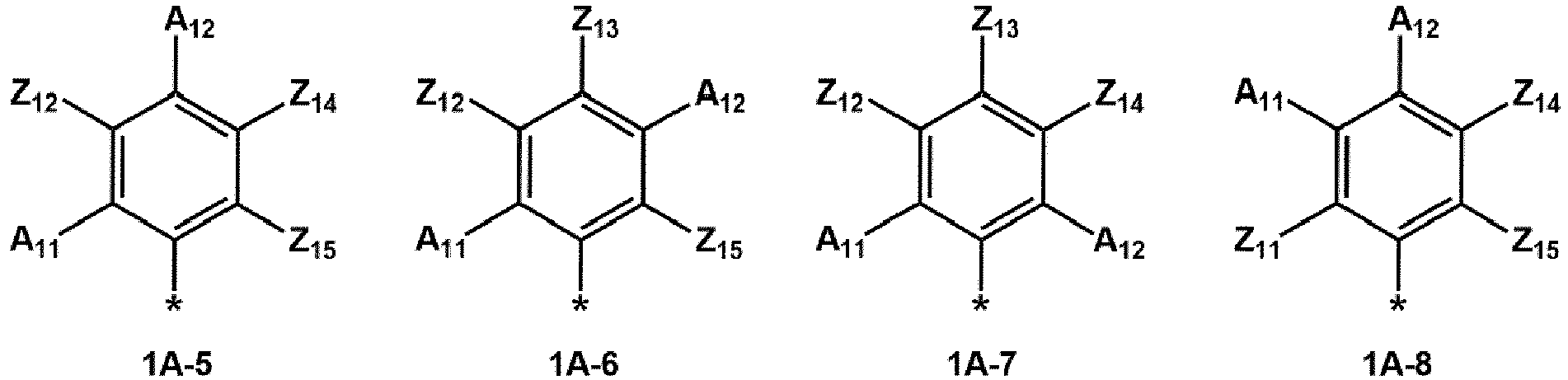


- Z11 to Z15 are each independently understood by referring to the description of Z1 provided herein,
- A11 to A13 are each independently substantially the same as described herein with reference to A1,
- A1 is understood by referring to the description of A1 in Formula 1A, and
- * indicates a binding site to an adjacent atom.
- In one or more embodiments, in Formulae 1A-1 to 1A-14, Z11 to Z15 may each independently be hydrogen, deuterium, -F, -CI, -Br, -I, -CH2D, -CHD2, -CD3, - CH2F, -CHF2, -CF3, a hydroxyl group, a cyano group, a nitro group, a methyl group, an ethyl group, a propyl group, an iso-propyl group, an n-butyl group, an iso-butyl group, a sec-butyl group, a tert-butyl group, an n-pentyl group, a tert-pentyl group, a neo-pentyl group, an iso-pentyl group, a sec-pentyl group, a 3-pentyl group, a sec-isopentyl group, an n-hexyl group, an iso-hexyl group, a sec-hexyl group, or a tert-hexyl group.
- In one or more embodiments, the group represented by Formula 1A may be a group represented by Formula 1A-7-1:

- Z12 to Z14 are each independently understood by referring to the description of Z1 provided herein,
- Z21 and Z22 are each independently understood by referring to the description of Z2 provided herein,
- k21 and k22 are each independently an integer from 1 to 7, and
- * indicates a binding site to an adjacent atom.
- In one or more embodiments, in Formula 1A-7-1,
- Z12 to Z14 may each independently be hydrogen, deuterium, -F, -CI, -Br, -I, - CH2D, -CHD2, -CD3, -CH2F, -CHF2, -CF3, a hydroxyl group, a cyano group, a nitro group, a methyl group, an ethyl group, a propyl group, an iso-propyl group, an n-butyl group, an iso-butyl group, a sec-butyl group, a tert-butyl group, an n-pentyl group, a tert-pentyl group, a neo-pentyl group, an iso-pentyl group, a sec-pentyl group, a 3-pentyl group, a sec-isopentyl group, an n-hexyl group, an iso-hexyl group, a sec-hexyl group, or a tert-hexyl group, and
- Z21 and Z22 may each be hydrogen.
- In one or more embodiments, in Formula 1, at least one of R1 in a number of b1, R2 in a number of b2, R3 in a number of b3, R4 in a number of b4, R5, R6, and R11 may be deuterium, -CH2D, -CHD2, -CD3, a phenyl group substituted with at least one deuterium, or a group represented by one of Formulae 10-2 to 10-7:
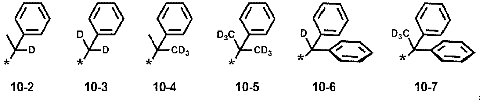
- wherein, in Formulae 10-2 to 10-7,
- "D" represents deuterium, and
- * indicates a binding site to an adjacent atom.
- In one or more embodiments, a moiety represented by


- wherein, in Formulae L1-1 and L1-2,
- R1a to R1d are each independently understood by referring to the description of R1 provided herein,
- R2a to R2c are each independently understood by referring to the description of R2 provided herein,
- M, A1, c1, Z1, and k1 are respectively understood by referring to the descriptions of M, A1, c1, Z1, and k1 provided herein, and
- * indicates a binding site to L2.
- In one or more embodiments, a moiety represented by


- wherein, in Formulae L2-1 and L2-2,
- R3a and R3b are each independently understood by referring to the description of R3 provided herein,
- R4a to R4e are each independently understood by referring to the description of R4 provided herein,
- R5a to R5d are each independently understood by referring to the description of R10a provided herein,
- M is understood by referring to the description of M in Formula 1, and
- * indicates a binding site to L2.
- In one embodiment, the organometallic compound may be represented by any one of Formulae 1-1 to 1-4:

- M, L2, A1, c1, Z1, and k1 are respectively understood by referring to the descriptions of M, L2, A1, c1, Z1, and k1 provided herein,
- R1a to R1d are each independently understood by referring to the description of R1 provided herein,
- R2a to R2c are each independently understood by referring to the description of R2 provided herein,
- R3a and R3b are each independently understood by referring to the description of R3 provided herein,
- R4a to R4e are each independently understood by referring to the description of R4 provided herein, and
- R5a to R5d are each independently understood by referring to the description of R10a provided herein.
- In one or more embodiments, in Formulae 1-1 to 1-4, R1a to R1d, R2a to R2c, R3a, R3b, R4a to R4e, and R5a to R5d may each independently be hydrogen, deuterium, - F, -CI, -Br, -I, -CH2D, -CHD2, -CD3, -CH2F, -CHF2, -CF3, a hydroxyl group, a cyano group, a nitro group, a methyl group, an ethyl group, a propyl group, an iso-propyl group, an n-butyl group, an iso-butyl group, a sec-butyl group, a tert-butyl group, an n-pentyl group, a tert-pentyl group, a neo-pentyl group, an iso-pentyl group, a sec-pentyl group, a 3-pentyl group, a sec-isopentyl group, an n-hexyl group, an iso-hexyl group, a sec-hexyl group, a tert-hexyl group, or a group represented by one selected from the group consisting of Formulae 9-1 to 9-31 and 10-1 to 10-7:


- "Et" represents an ethyl group,
- "i-Pr" represents an iso-propyl group,
- "t-Bu" represents a tert-butyl group,
- "D" represents deuterium, and
- * indicates a binding site to an adjacent atom.
- In some embodiments, in Formula 1-1 to 1-4, at least one of R1a to R1d, R2a to R2c, R3a, R3b, R4a to R4e, and R5a to R5d may be represented by deuterium, -CH2D, - CHD2, -CD3, or a group represented by one of Formulae 10-1 to 10-7:

- "D" represents deuterium, and
- * indicates a binding site to an adjacent atom.
- In one or more embodiments, the organometallic compound may be one of Compounds BD01 to BD210:








- In the organometallic compound represented by Formula 1, a triplet (T1) energy level of the A1 group represented by Formula 1B may be about 0.01 eV or higher than a triplet energy level of another moiety in the molecule. Because a bulky group such as a group represented by Formula 1A is substituted on the ligand, the group represented by Formula 1A may induce steric hindrance to thereby suppress or reduce substituent rotation and maintain structural rigidity of the molecule. Accordingly, when the organometallic compound is used as a dopant, intermolecular interaction between homogeneous or heterogeneous molecules may be suppressed or reduced to thereby suppress or reduce self-aggregation or aggregation with a host material. Due to such a structural characteristic, two types (or kinds) of energy transfer, including metal to ligand charge transfer (3MLCT) and intraligand charge transfer (3ILCT), may be activated. Accordingly, a light-emitting device including the organometallic compound may have improved efficiency and lifespan.
- In addition, the organometallic compound represented by Formula 1 may include at least one carbon-deuterium (C-D) bond. A C-D bond may have a short bonding length, as compared with a C-H bond, and the binding energy may increase about 13 kcal/mol. Thus, the internal energy of the organometallic compound may decrease, and stability of the complex molecule may improve. Accordingly, upon energy transition in the molecule, nonradiative transition may be prevented or reduced to thereby improve a photoluminescence quantum yield (PLQY).
- In the organometallic compound represented by Formula 1, a carbene-containing ligand and the group represented by Formula 1A may be disposed (e.g., positioned) to be substantially perpendicular to a carbene-containing core. Thus, the overall molecular conjugation may be broken or decreased. Accordingly, an emission wavelength may be blue-shifted, and thus, when the organometallic compound is applied to a light-emitting device, the light-emitting device may emit deep-blue light. Accordingly, the light-emitting device may exhibit improved colorimetric purity and color reproducibility.
- Therefore, an electronic device, e.g., a light-emitting device, including the organometallic compound may have a low driving voltage, high efficiency, long lifespan, and/or high colorimetric purity.
- Methods of synthesizing the organometallic compound represented by Formula 1 may be easily understood to those of ordinary skill in the art by referring to Synthesis Examples and Examples described herein.
- At least one of the organometallic compounds represented by Formula 1 may be used in a light-emitting device (e.g., an organic light-emitting device).
- According to one or more embodiments, a light-emitting device includes a first electrode; a second electrode facing the first electrode; an interlayer located between the first electrode and the second electrode and including an emission layer and the organometallic compound represented by Formula 1.
- In some embodiments,
- the first electrode of the light-emitting device may be an anode,
- the second electrode of the light-emitting device may be a cathode,
- the interlayer may further include a hole transport region located between the first electrode and the emission layer, and an electron transport region located between the emission layer and the second electrode,
- the hole transport region may include a hole injection layer, a hole transport layer, an emission auxiliary layer, an electron blocking layer, or any combination thereof, and
- the electron transport region may include a buffer layer, a hole blocking layer, an electron control layer, an electron transport layer, an electron injection layer, or any combination thereof.
- In one or more embodiments, the organometallic compound may be included in an interlayer, e.g., an emission layer, of the light-emitting device.
- In one or more embodiments, the emission layer may include a host and a dopant, and the dopant may include the organometallic compound. For example, the organometallic compound may serve as an emission layer dopant. A content (e.g., amount) of the dopant in the emission layer may be in a range of about 0.1 parts to about 49.99 parts by weight, based on 100 parts by weight of the emission layer.
- The emission layer may emit red light, green light, blue light, and/or white light. In some embodiments, the emission layer may emit blue light. Blue light having a maximum emission wavelength in a range of about 440 nm to about 475 nm may be emitted from the emission layer. A bottom emission-based CIEx color-coordinate of the blue light may be in a range of about 0.13 to about 0.14, and a CIEy color-coordinate may be in a range of about 0.06 to about 0.25, but embodiments are not limited thereto.
- In one or more embodiments, the host may include different types (or kinds) of hosts. In some embodiments, the host may include a hole transporting host and an electron transporting host.
- In one or more embodiments, the host may include an electron transporting host represented by Formula 2, a hole transporting host represented by Formula 3, or any combination thereof:


- [00166] X21 is N or C-(L24)a24-(R24)b24, X22 is N or C-(L25)a25-(R25)b25, and X23 is N or C-(L26)a26-(R26)b26,
- X31 is selected from a single bond, O, S, N(R34), C(R34)(R35), and Si(R34)(R35),
- CY31 and CY32 are each independently a C3-C60 (e.g. C3-C30) carbocyclic group or a C1-C60 (e.g. C1-C20) heterocyclic group,
- L21 to L26 and L31 to L33 are each independently a C3-C60 (e.g. C3-C30) carbocyclic group unsubstituted or substituted with at least one R10a or a C1-C60 (e.g. C1-C20) heterocyclic group unsubstituted or substituted with at least one R10a,
- a21 to a26 and a31 to a33 are each independently an integer from 0 to 5,
- R21 to R26 and R31 to R35 are each independently hydrogen, deuterium, -F, - CI, -Br, -I, a hydroxyl group, a cyano group, a nitro group, a C1-C60 (e.g. C1-C20) alkyl group unsubstituted or substituted with at least one R10a, a C2-C60 (e.g. C2-C20) alkenyl group unsubstituted or substituted with at least one R10a, a C2-C60 (e.g. C2-C20) alkynyl group unsubstituted or substituted with at least one R10a, a C1-C60 (e.g. C1-C20) alkoxy group unsubstituted or substituted with at least one R10a, a C3-C60 (e.g. C3-C30) carbocyclic group unsubstituted or substituted with at least one R10a, a C1-C60 (e.g. C1-C20) heterocyclic group unsubstituted or substituted with at least one R10a, a C6-C60 (e.g. C6-C30) aryloxy group unsubstituted or substituted with at least one R10a, a C6-C60 (e.g. C6-C30) arylthio group unsubstituted or substituted with at least one R10a, - Si(Q1)(Q2)(Q3), -N(Q1)(Q2), -B(Q1)(Q2), -C(=O)(Q1), -S(=O)2(Q1), or -P(=O)(Q1)(Q2),
- b21 to b26, b31 to b33, n31, and n32 are each independently an integer from 1 to 5, and
- R10a and Q1 to Q3 are respectively understood by referring to the descriptions of R10a and Q1 to Q3 provided herein.
- In Formula 2, when a21 is 0, (L21)a21 may be a single bond, when a22 is 0, (L22)a22 may be a single bond, when a23 is 0, (L23)a23 may be a single bond, when a24 is 0, (L24)a24 may be a single bond, when a25 is 0, (L25)a25 may be a single bond, and when a26 is 0, (L26)a26 may be a single bond.
- In some embodiments, in Formula 2, a21 to a26 may each independently be 0 or 1.
- In one or more embodiments, in Formula 2, L21 to L26 may each independently be a phenylene group unsubstituted or substituted with at least one R10a.
- In some embodiments, in Formula 3, CY31 and CY32 may each independently be a benzene group, a naphthalene group, an anthracene group, a phenanthrene group, a triphenylene group, a pyrene group, a chrysene group, a cyclopentadiene group, a 1,2,3,4-tetrahydronaphthalene group, a thiophene group, a furan group, an indole group, a benzoborole group, a benzophosphole group, an indene group, a benzosilole group, a benzogermole group, a benzothiophene group, a benzoselenophene group, a benzofuran group, a carbazole group, a dibenzoborole group, a dibenzophosphole group, a fluorene group, a dibenzosilole group, a dibenzogermole group, a dibenzothiophene group, a dibenzoselenophene group, a dibenzofuran group, a dibenzothiophene 5-oxide group, a 9H-fluorene-9-one group, a dibenzothiophene 5,5-dioxide group, an azaindole group, an azabenzoborole group, an azabenzophosphole group, an azaindene group, an azabenzosilole group, an azabenzogermole group, an azabenzothiophene group, an azabenzoselenophene group, an azabenzofuran group, an azacarbazole group, an azadibenzoborole group, an azadibenzophosphole group, an azafluorene group, an azadibenzosilole group, an azadibenzogermole group, an azadibenzothiophene group, an azadibenzoselenophene group, an azadibenzofuran group, an azadibenzothiophene 5-oxide group, an aza-9H-fluoren-9-one group, an azadibenzothiophene 5,5-dioxide group, a pyridine group, a pyrimidine group, a pyrazine group, a pyridazine group, a triazine group, a quinoline group, an isoquinoline group, a quinoxaline group, a quinazoline group, a phenanthroline group, a pyrrole group, a pyrazole group, an imidazole group, a triazole group, an oxazole group, an isooxazole group, a thiazole group, an isothiazole group, an oxadiazole group, a thiadiazole group, a benzopyrazole group, a benzimidazole group, a benzoxazole group, a benzothiazole group, a benzoxadiazole group, a benzothiadiazole group, a 5,6,7,8-tetrahydroisoquinoline group, or a 5,6,7,8-tetrahydroquinoline group, but embodiments are not limited thereto.
- In one or more embodiments, in Formulae 2 and 3, R21 to R26 and R31 to R35 may each independently be:
- hydrogen, deuterium, -F, -CI, -Br, -I, -CH2D, -CHD2, -CD3, -CH2F, -CHF2, - CF3, a hydroxyl group, a cyano group, or a nitro group;
- a C1-C60 (e.g. C1-C20) alkyl group or a C1-C60 (e.g. C1-C20) alkoxy group, each unsubstituted or substituted with deuterium, -F, -CI, -Br, -I, -CH2D, -CHD2, -CD3, - CH2F, -CHF2, -CF3, a hydroxyl group, a cyano group, a nitro group, a cyclopentyl group, a cyclohexyl group, a cycloheptyl group, an adamantyl group, a norbornyl group, a norbornenyl group, a cyclopentenyl group, a cyclohexenyl group, a cycloheptenyl group, a phenyl group, a biphenyl group, a naphthyl group, a pyridinyl group, a pyrimidinyl group, or any combination thereof;
- a cyclopentyl group, a cyclohexyl group, a cycloheptyl group, an adamantyl group, a norbornyl group, a norbornenyl group, a cyclopentenyl group, a cyclohexenyl group, a cycloheptenyl group, a phenyl group, a biphenyl group, a terphenyl group, a pentalenyl group, an indenyl group, a naphthyl group, an azulenyl group, an indacenyl group, an acenaphthyl group, a fluorenyl group, a spiro-bifluorenyl group, a benzofluorenyl group, a dibenzofluorenyl group, a phenalenyl group, a phenanthrenyl group, an anthracenyl group, a fluoranthenyl group, a triphenylenyl group, a pyrenyl group, a chrysenyl group, a perylenyl group, a pentacenyl group, a pyrrolyl group, a thiophenyl group, a furanyl group, a silolyl group, an imidazolyl group, a pyrazolyl group, a thiazolyl group, an isothiazolyl group, an oxazolyl group, an isoxazolyl group, a pyridinyl group, a pyrazinyl group, a pyrimidinyl group, a pyridazinyl group, an indolyl group, an isoindolyl group, an indazolyl group, a purinyl group, a quinolinyl group, an isoquinolinyl group, a benzoquinolinyl group, a benzoisoquinolinyl group, a phthalazinyl group, a naphthyridinyl group, a quinoxalinyl group, a benzoquinoxalinyl group, a quinazolinyl group, a benzoquinazolinyl group, a cinnolinyl group, a phenanthridinyl group, an acridinyl group, a phenanthrolinyl group, a phenazinyl group, a benzimidazolyl group, a benzofuranyl group, a benzothiophenyl group, a benzosilolyl group, a benzothiazolyl group, a benzoisothiazolyl group, a benzoxazolyl group, a benzoisoxazolyl group, a triazolyl group, a tetrazolyl group, a thiadiazolyl group, an oxadiazolyl group, a triazinyl group, a carbazolyl group, a dibenzofuranyl group, a dibenzothiophenyl group, a dibenzosilolyl group, a benzocarbazolyl group, a naphthobenzofuranyl group, a naphthobenzothiophenyl group, a naphthobenzosilolyl group, a dibenzocarbazolyl group, a dinaphthofuranyl group, a dinaphthothiophenyl group, a dinaphthosilolyl group, an imidazopyridinyl group, an imidazopyrimidinyl group, an oxazolopyridinyl group, a thiazolopyridinyl group, a benzonaphthyridinyl group, an azafluorenyl group, an azaspiro-bifluorenyl group, an azacarbazolyl group, an azadibenzofuranyl group, an azadibenzothiophenyl group, an azadibenzosilolyl group, an indenopyrrolyl group, an indolopyrrolyl group, an indenocarbazolyl group, or an indolocarbazolyl group, each unsubstituted or substituted with deuterium, -F, -CI, - Br, -I, -CH2D, -CHD2, -CD3, -CH2F, -CHF2, -CF3, a hydroxyl group, a cyano group, a nitro group, a C1-C60 (e.g. C1-C20) alkyl group, a C1-C60 (e.g. C1-C20) alkoxy group, a cyclopentyl group, a cyclohexyl group, a cycloheptyl group, an adamantyl group, a norbornyl group, a norbornenyl group, a cyclopentenyl group, a cyclohexenyl group, a cycloheptenyl group, a phenyl group, a biphenyl group, a terphenyl group, a pentalenyl group, an indenyl group, a naphthyl group, an azulenyl group, an indacenyl group, an acenaphthyl group, a fluorenyl group, a spiro-bifluorenyl group, a benzofluorenyl group, a dibenzofluorenyl group, a phenalenyl group, a phenanthrenyl group, an anthracenyl group, a fluoranthenyl group, a triphenylenyl group, a pyrenyl group, a chrysenyl group, a perylenyl group, a pentacenyl group, a pyrrolyl group, a thiophenyl group, a furanyl group, a silolyl group, an imidazolyl group, a pyrazolyl group, a thiazolyl group, an isothiazolyl group, an oxazolyl group, an isoxazolyl group, a pyridinyl group, a pyrazinyl group, a pyrimidinyl group, a pyridazinyl group, an indolyl group, an isoindolyl group, an indazolyl group, a purinyl group, a quinolinyl group, an isoquinolinyl group, a benzoquinolinyl group, a benzoisoquinolinyl group, a phthalazinyl group, a naphthyridinyl group, a quinoxalinyl group, a benzoquinoxalinyl group, a quinazolinyl group, a benzoquinazolinyl group, a cinnolinyl group, a phenanthridinyl group, an acridinyl group, a phenanthrolinyl group, a phenazinyl group, a benzimidazolyl group, a benzofuranyl group, a benzothiophenyl group, a benzosilolyl group, a benzothiazolyl group, a benzoisothiazolyl group, a benzoxazolyl group, a benzoisoxazolyl group, a triazolyl group, a tetrazolyl group, a thiadiazolyl group, an oxadiazolyl group, a triazinyl group, a carbazolyl group, a dibenzofuranyl group, a dibenzothiophenyl group, a dibenzosilolyl group, a benzocarbazolyl group, a naphthobenzofuranyl group, a naphthobenzothiophenyl group, a naphthobenzosilolyl group, a dibenzocarbazolyl group, a dinaphthofuranyl group, a dinaphthothiophenyl group, a dinaphthosilolyl group, an imidazopyridinyl group, an imidazopyrimidinyl group, an oxazolopyridinyl group, a thiazolopyridinyl group, a benzonaphthyridinyl group, an azafluorenyl group, an azaspiro-bifluorenyl group, an azacarbazolyl group, an azadibenzofuranyl group, an azadibenzothiophenyl group, an azadibenzosilolyl group, an indenopyrrolyl group, an indolopyrrolyl group, an indenocarbazolyl group, an indolocarbazolyl group, - Si(Q31)(Q32)(Q33), -N(Q31)(Q32), -B(Q31)(Q32), -C(=O)(Q31), -S(=O)2(Q31),-P(=O)(Q31)(Q32), or any combination thereof; or
- -Si(Q1)(Q2)(Q3), -N(Q1)(Q2), -B(Q1)(Q2), -C(=O)(Q1), -S(=O)2(Q1), or - P(=O)(Q1)(Q2),
- wherein Q1 to Q3 and Q31 to Q33 may respectively be understood by referring to the descriptions of Q1 to Q3 and Q31 to Q33 provided herein.
- In some embodiments, in Formula 2, R21 to R26 may each independently be:
- a phenyl group or a carbazolyl group, each unsubstituted or substituted with a C1-C10 alkyl group, a phenyl group, a carbazolyl group, -Si(Q31)(Q32)(Q33), or any combination thereof; or
-
-Si(Q1)(Q2)(Q3)
, - wherein Q1 to Q3 and Q31 to Q33 may respectively be understood by referring to the descriptions of Q1 to Q3 and Q31 to Q33 provided herein.
- In one or more embodiments, in Formula 2, at least one of R21 in a number of b21, R22 in a number of b22, and R23 in a number of b23 may be: a phenyl group, a carbazolyl group, each unsubstituted or substituted with a phenyl group, a carbazolyl group, Si(Q1)(Q2)(Q3), or any combination thereof.
- In one or more embodiments, the electron transporting host represented by Formula 2 may include at least one deuterium. In some embodiments, at least one selected from R21 to R26 may be deuterium, or at least one selected from L21 to L26 and R21 to R26 may be substituted with at least one deuterium.
- In one or more embodiments, the hole transporting host represented by Formula 3 may include at least one deuterium. In some embodiments, at least one selected from R31 to R35 may be deuterium, or at least one selected from L31 to L33 and R31 to R35 may be substituted with at least one deuterium.
- For example, the electron transporting host represented by Formula 2 may be one of Compounds ETH1 to ETH16, and the hole transporting host represented by Formula 3 may be one of Compounds HTH1 to HTH16, but embodiments are not limited thereto:


- The electron transporting host represented by Formula 2 and the hole transporting host represented by Formula 3 may form an exciplex.
- In one or more embodiments, the host may include the electron transporting host represented by Formula 2 and the hole transporting host represented by Formula 3. In this embodiment, the electron transporting host and the hole transporting host may form an exciplex. Thus, when the electron transporting host and the hole transporting host are used as co-hosts in the emission layer, a light-emitting device may have high efficiency and long lifespan.
- A content ratio of the electron transporting host to the hole transporting host in the emission layer may be in a range of about 90:10 to about 10:90, for example, about 80:20 to about 20:80, or for example, about 70:30 to about 30:70, but embodiments are not limited thereto.
- In one or more embodiments, the dopant may further include a delayed fluorescent material.
- For example, the delayed fluorescent material may be a compound represented by Formula 4:

- W41 is O, S, N(R41a) or C(R41a)(R41b), W42 iS O, S, N(R42a), or C(R42a)(R42b), W43 is O, S, N(R43a), or C(R43a)(R43b), and W44 is O, S, N(R44a), or C(R44a)(R44b),
- R41a, R41b, R42a, R42b, R43a, R43b, R44a, R44b, R45a, R45b, R46, R47, R48, and R49 are each independently hydrogen, deuterium, -F, -CI, -Br, -I, a hydroxyl group, a cyano group, a nitro group, a C1-C60 (e.g. C1-C20) alkyl group unsubstituted or substituted with at least one R10a, a C2-C60 (e.g. C2-C20) alkenyl group unsubstituted or substituted with at least one R10a, a C2-C60 (e.g. C2-C20) alkynyl group unsubstituted or substituted with at least one R10a, a C1-C60 (e.g. C1-C20) alkoxy group unsubstituted or substituted with at least one R10a, a C3-C60 (e.g. C3-C30) carbocyclic group unsubstituted or substituted with at least one R10a, a C1-C60 (e.g. C1-C20) heterocyclic group unsubstituted or substituted with at least one R10a, a C6-C60 (e.g. C6-C30) aryloxy group unsubstituted or substituted with at least one R10a, a C6-C60 (e.g. C6-C30) arylthio group unsubstituted or substituted with at least one R10a, -Si(Q1)(Q2)(Q3), -N(Q1)(Q2), -B(Q1)(Q2), -C(=O)(Q1), - S(=O)2(Q1), or -P(=O)(Q1)(Q2),
- b46 and b49 are each independently an integer from 1 to 4,
- b47 and b48 are each independently an integer from 1 to 3,
- R10a and Q1 to Q3 may respectively be understood by referring to the descriptions of R10a and Q1 to Q3 provided herein.
- An excited triplet energy level of the organometallic compound represented by Formula 1 and an excited triplet energy level of the compound represented by Formula 4 may be small such that dexter energy transition may occur.
- A difference between an excited triplet energy level of the compound represented by Formula 4 and an excited singlet energy level thereof may be very small (e.g., about 0.3 eV or less). Thus, due to reverse intersystem crossing (RISC) mechanism, excitons of the excited triplet energy level may be transferred to excitons of the excited singlet energy level.
- Accordingly, in a case of a light-emitting device further including the compound represented by Formula 4 according to one or more embodiments, excited triplet excitons transitioned from the organometallic compound may not be quenched and may be transitioned to an excited singlet state, and then transitioned to a ground state. Thus, an (organic) light-emitting device having high efficiency and long lifespan may be manufactured.
- In one or more embodiments, the compound represented by Formula 4 may be a fluorescence emitter. For example, the compound represented by Formula 4 may be a delayed fluorescence dopant.
- In one or more embodiments, W41 may be N(R41a), W42 may be N(R42a), W43 may be N(R43a), and/or W44 may be N(R44a). For example, W41 may be N(R41a), and W42 may be N(R42a). For example, W41 may be N(R41a), W42 may be N(R42a), and W43 may be N(R43a). For example, W41 may be N(R41a), W42 may be N(R42a), and W44 may be N(R44a). For example, W42 may be N(R42a), W43 may be N(R43a), and W44 may be N(R44a). For example, W41 may be N(R41a), W42 may be N(R42a), W43 may be N(R43a), and W44 may be N(R44a).
- In one or more embodiments, R47 and R48 may each be -N(Q1)(Q2), wherein Q1 and Q2 may each independently be a C6-C60 (e.g. C6-C30) aryl group unsubstituted or substituted with deuterium, -F, a cyano group, a C1-C10 alkyl group, a phenyl group, a biphenyl group, or any combination thereof, and b47 and b48 may each be 1.
- For example, the compound represented by Formula 4 may be one of Compounds DFD1 to DFD12, but embodiments are not limited thereto:


- In one or more embodiments, the light-emitting device may include at least one of a first capping layer located outside the first electrode and a second capping layer located outside the second electrode. In some embodiments, the at least one of the first capping layer and the second capping layer may include the organometallic compound represented by Formula 1. The first capping layer and the second capping layer may respectively be understood by referring to the descriptions of the first capping layer and the second capping layer provided herein.
- In some embodiments, the at least one of the first capping layer and the second capping layer may have a refractive index of about 1.6 or higher at a wavelength of 589 nanometers (nm).
- The expression that an "(interlayer and/or a capping layer) includes at least one organometallic compound" as used herein may be construed as meaning that the "(interlayer and/or the capping layer) may include one organometallic compound of Formula 1 or two or more different organometallic compounds of Formula 1".
- For example, Compound BD01 may only be included in the interlayer as the organometallic compound. In this embodiment, Compound BD01 may be included in the emission layer of the light-emitting device. In some embodiments, Compounds BD01 and BD02 may be included in the interlayer as the organometallic compounds. In this embodiment, Compounds BD01 and BD02 may be included in the same layer (for example, both Compounds BD01 and BD02 may be included in an emission layer) or in different layers (for example, Compound BD01 may be included in an emission layer, and Compound BD02 may be included in an electron transport region).
- According to one or more embodiments, an electronic apparatus may include the light-emitting device. The electronic apparatus may further include a thin-film transistor. In some embodiments, the electronic apparatus may further include a thin-film transistor including a source electrode and a drain electrode, and a first electrode of the light-emitting device may be electrically connected (e.g., electrically coupled) to the source electrode or the drain electrode. The electronic apparatus may further include a color filter, a color-conversion layer, a touchscreen layer, a polarization layer, or any combination thereof. The electronic apparatus may be understood by referring to the description of the electronic apparatus provided herein.
-
FIG. 1 is a schematic view of a light-emittingdevice 10 according to one or more embodiments. The light-emittingdevice 10 includes afirst electrode 110, aninterlayer 130, and asecond electrode 150. - Hereinafter, the structure of the light-emitting
device 10 according to one or more embodiments and a method of manufacturing the light-emittingdevice 10 according to one or more embodiments will be described in connection withFIG. 1 . - In
FIG. 1 , a substrate may be additionally located under thefirst electrode 110 or above thesecond electrode 150. The substrate may be a glass substrate and/or a plastic substrate. The substrate may be a flexible substrate including plastic having excellent (or suitable) heat resistance and durability, for example, polyimide, polyethylene terephthalate (PET), polycarbonate, polyethylene naphthalate, polyarylate (PAR), polyetherimide, or any combination thereof. - The
first electrode 110 may be formed by depositing or sputtering, on the substrate, a material for forming thefirst electrode 110. When thefirst electrode 110 is an anode, a high work function material that may easily inject holes may be used as a material for a first electrode. - The
first electrode 110 may be a reflective electrode, a semi-transmissive electrode, or a transmissive electrode. When thefirst electrode 110 is a transmissive electrode, a material for forming thefirst electrode 110 may be indium tin oxide (ITO), indium zinc oxide (IZO), tin oxide (SnO2), zinc oxide (ZnO), or any combinations thereof. In some embodiments, when thefirst electrode 110 is a semi-transmissive electrode or a reflective electrode, magnesium (Mg), silver (Ag), aluminum (Al), aluminum-lithium (Al-Li), calcium (Ca), magnesium-indium (Mg-In), magnesium-silver (Mg-Ag), or any combination thereof may be used as a material for forming thefirst electrode 110. - The
first electrode 110 may have a single-layered structure including (e.g., consisting of) a single layer or a multi-layered structure including two or more layers. In some embodiments, thefirst electrode 110 may have a triple-layered structure of ITO/Ag/ITO. - The
interlayer 130 is on thefirst electrode 110. Theinterlayer 130 includes an emission layer. - The
interlayer 130 may further include a hole transport region between thefirst electrode 110 and the emission layer and an electron transport region between the emission layer and thesecond electrode 150. - The
interlayer 130 may further include metal-containing compounds such as organometallic compounds, inorganic materials such as quantum dots, and/or the like, in addition to one or more suitable organic materials. - The
interlayer 130 may include: i) at least two emitting units sequentially stacked between thefirst electrode 110 and thesecond electrode 150; and ii) a charge-generation layer located between the at least two emitting units. When theinterlayer 130 includes the at least two emitting units and the charge generation layer, the light-emittingdevice 10 may be a tandem light-emitting device. - The hole transport region may have i) a single-layered structure including (e.g., consisting of) a single layer including (e.g., consisting of) a single material, ii) a single-layered structure including (e.g., consisting of) a single layer including a plurality of different materials, or iii) a multi-layered structure having a plurality of layers including a plurality of different materials.
- The hole transport region may include a hole injection layer, a hole transport layer, an emission auxiliary layer, an electron blocking layer, or a combination thereof.
- For example, the hole transport region may have a multi-layered structure, e.g., a hole injection layer/hole transport layer structure, a hole injection layer/hole transport layer/emission auxiliary layer structure, a hole injection layer/emission auxiliary layer structure, a hole transport layer/emission auxiliary layer structure, or a hole injection layer/hole transport layer/electron blocking layer structure, wherein the layers of each structure are sequentially stacked on the
first electrode 110 in each stated order. - The hole transport region may include the compound represented by Formula 201, the compound represented by Formula 202, or any combination thereof:


- L201 to L204 may each independently be a C3-C60 (e.g. C3-C30) carbocyclic group unsubstituted or substituted with at least one R10a or a C1-C60 (e.g. C1-C20) heterocyclic group unsubstituted or substituted with at least one R10a,
- L205 may be *-O-*', *-S-*', *-N(Q201)-*', a C1-C20 (e.g. C1-C10) alkylene group unsubstituted or substituted with at least one R10a, a C2-C20 (e.g. C2-C10) alkenylene group unsubstituted or substituted with at least one R10a, a C3-C60 (e.g. C3-C30) carbocyclic group unsubstituted or substituted with at least one R10a, or a C1-C60 (e.g. C1-C20) heterocyclic group unsubstituted or substituted with at least one R10a,
- xa1 to xa4 may each independently be an integer from 0 to 5,
- xa5 may be an integer from 1 to 10,
- R201 to R204 and Q201 may each independently be a C3-C60 (e.g. C3-C30) carbocyclic group unsubstituted or substituted with at least one R10a or a C1-C60 (e.g. C1-C20) heterocyclic group unsubstituted or substituted with at least one R10a,
- R201 and R202 may optionally be bound to each other via a single bond, a C1-C5 alkylene group unsubstituted or substituted with at least one R10a, or a C2-C5 alkenylene group unsubstituted or substituted with at least one R10a to form a C8-C60 (e.g. C8-C30) polycyclic group (e.g., a carbazole group and/or the like) unsubstituted or substituted with at least one R10a (e.g., Compound HT16 described herein),
- R203 and R204 may optionally be bound to each other via a single bond, a C1-C5 alkylene group unsubstituted or substituted with at least one R10a, or a C2-C5 alkenylene group unsubstituted or substituted with at least one R10a to form a C8-C60 (e.g. C8-C30) polycyclic group unsubstituted or substituted with at least one R10a,
- na1 may be an integer from 1 to 4.
- In some embodiments, Formulae 201 and 202 may each include at least one of the groups represented by Formulae CY201 to CY217:


- In some embodiments, in Formulae CY201 to CY217, ring CY201 to ring CY204 may each independently be a benzene group, a naphthalene group, a phenanthrene group, or an anthracene group.
- In one or more embodiments, Formulae 201 and 202 may each include at least one of the groups represented by Formula CY201 to CY203.
- In one or more embodiments, Formula 201 may include at least one of groups represented by Formulae CY201 to CY203 and at least one of the groups represented by Formulae CY204 to CY217.
- In one or more embodiments, in Formula 201, xa1 may be 1, R201 may be a group represented by any one of Formulae CY201 to CY203, xa2 may be 0, and R202 may be a group represented by Formulae CY204 to CY207.
- In one or more embodiments, Formula 201 and 202 may each not include groups represented by Formulae CY201 to CY203.
- In one or more embodiments, Formula 201 and 202 may each not include groups represented by Formulae CY201 to CY203, and include at least one of the groups represented by Formulae CY204 to CY217.
- In one or more embodiments, Formula 201 and 202 may each not include groups represented by Formulae CY201 to CY217.
- In some embodiments, the hole transport region may include one of Compounds HT1 to HT46, m-MTDATA, TDATA, 2-TNATA, NPB (NPD), β-NPB, TPD, spiro-TPD, spiro-NPB, methylated-NPB, TAPC, HMTPD, 4,4',4"-tris(N-carbazolyl)triphenylamine (TCTA), polyaniline/dodecylbenzenesulfonic acid (PANI/DBSA), poly(3,4-ethylenedioxythiophene)/poly(4-styrenesulfonate) (PEDOT/PSS), polyaniline/camphorsulfonic acid (PANI/CSA), polyaniline/poly(4-styrenesulfonate (PANI/PSS), or any combination thereof:


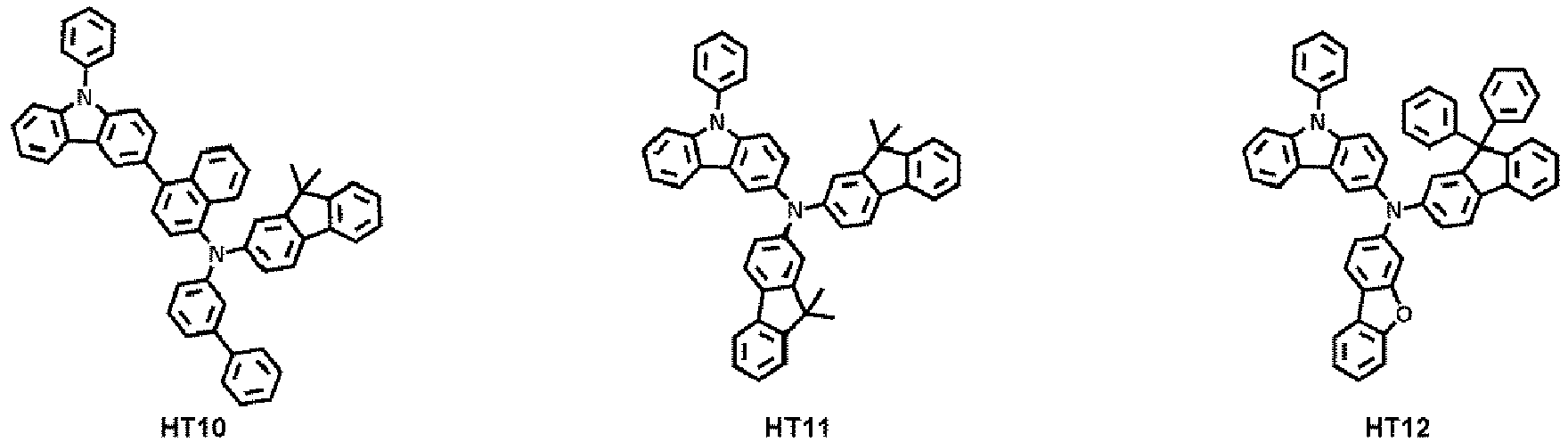


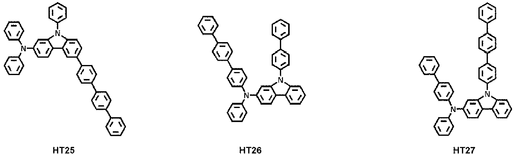


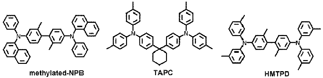
- The thickness of the hole transport region may be in a range of about 50 Angstroms (Å) to about 10,000 Å, for example, about 100 Å to about 7,000 Å, about 100 Å to about 5,000 Å, about 100 Å to about 4,000 Å or about 100 Å to about 1,000 Å. When the hole transport region includes a hole injection layer, a hole transport layer, or any combination thereof, the thickness of the hole injection layer may be in a range of about 100 Å to about 9,000 Å, for example, about 100 Å to about 7,000 Å, about 100 Å to about 5,000 Å, about 100 Å to about 3,000 Å, about 100 Å to about 2,000 Å, about 100 Å to about 1,000 Å or about 500 Å to about 700 Å, and the thickness of the hole transport layer may be in a range of about 50 Å to about 2,000 Å, for example, about 100 Å to about 1,500 Å or about 200 Å to about 400 Å. When the thicknesses of the hole transport region, the hole injection layer, and the hole transport layer are within any of these ranges, excellent (or improved) hole transport characteristics may be obtained without a substantial increase in driving voltage.
- The emission auxiliary layer may increase light emission efficiency by compensating for an optical resonance distance according to the wavelength of light emitted by an emission layer. The electron blocking layer may reduce or eliminate the flow of electrons from an electron transport region. The emission auxiliary layer and the electron blocking layer may each independently include any of the aforementioned materials.
- The hole transport region may include a charge generating material, as well as the aforementioned materials, to improve conductive properties of the hole transport region. The charge generating material may be substantially homogeneously or non-homogeneously dispersed (for example, as a single layer consisting of charge generating material) in the hole transport region.
- The charge generating material may include, for example, a p-dopant.
- In some embodiments, a lowest unoccupied molecular orbital (LUMO) energy level of the p-dopant may be about -3.5 eV or less.
- In some embodiments, the p-dopant may include a quinone derivative, a cyano group-containing compound, elements EL1 and/or EL2-containing compound, or any combination thereof.
- Examples of the quinone derivative may include TCNQ, F4-TCNQ, and the like.
- Examples of the cyano group-containing compound may include HAT-CN, a compound represented by Formula 221, and the like:


- R221 to R223 may each independently be a C3-C60 (e.g. C3-C30) carbocyclic group unsubstituted or substituted with at least one R10a or a C1-C60 (e.g. C1-C20) heterocyclic group unsubstituted or substituted with at least one R10a, and
- at least one of R221 to R223 may each independently be: a C3-C60 (e.g. C3-C30) carbocyclic group or a C1-C60 (e.g. C1-C20) heterocyclic group, each independently substituted with a cyano group; -F; -CI; -Br; -I; a C1-C20 (e.g. C1-C10) alkyl group substituted with a cyano group, -F, -CI, -Br, -I, or any combination thereof; or any combination thereof.
- In the elements EL1 and/or EL2-containing compound, element EL1 may be metal, metalloid, or a combination thereof, and element EL2 may be non-metal, metalloid, or a combination thereof.
- Examples of the metal may include: an alkali metal (e.g., lithium (Li), sodium (Na), potassium (K), rubidium (Rb), cesium (Cs), and/or the like); an alkaline earth metal (e.g., beryllium (Be), magnesium (Mg), calcium (Ca), strontium (Sr), barium (Ba), and/or the like); a transition metal (e.g., titanium (Ti), zirconium (Zr), hafnium (Hf), vanadium (V), niobium (Nb), tantalum (Ta), chromium (Cr), molybdenum (Mo), tungsten (W), manganese (Mn), technetium (Tc), rhenium (Re), iron (Fe), ruthenium (Ru), osmium (Os), cobalt (Co), rhodium (Rh), iridium (Ir), nickel (Ni), palladium (Pd), platinum (Pt), copper (Cu), silver (Ag), gold (Au), and/or the like); post-transition metal (e.g., zinc (Zn), indium (In), tin (Sn), and/or the like); a lanthanide metal (e.g., lanthanum (La), cerium (Ce), praseodymium (Pr), neodymium (Nd), promethium (Pm), samarium (Sm), europium (Eu), gadolinium (Gd), terbium (Tb), dysprosium (Dy), holmium (Ho), erbium (Er), thulium (Tm), ytterbium (Yb), lutetium (Lu), and/or the like); and/or the like.
- Examples of the metalloid may include silicon (Si), antimony (Sb), tellurium (Te), and/or the like.
- Examples of the non-metal may include oxygen (O), halogen (e.g., F, CI, Br, I, and/or the like), and/or the like.
- For example, the elements EL1 and/or EL2-containing compound may include a metal oxide, a metal halide (e.g., metal fluoride, metal chloride, metal bromide, metal iodide, and/or the like), a metalloid halide (e.g., a metalloid fluoride, a metalloid chloride, a metalloid bromide, a metalloid iodide, and/or the like), a metal telluride, or any combination thereof.
- Examples of the metal oxide may include tungsten oxide (e.g., WO, W2O3, WO2, WO3, W2O5, and/or the like), vanadium oxide (e.g., VO, V2O3, VO2, V2O5, and/or the like), molybdenum oxide (MoO, Mo2O3, MoO2, MoO3, Mo2O5, and/or the like), rhenium oxide (e.g., ReO3, and/or the like), and the like.
- Examples of the metal halide may include alkali metal halide, alkaline earth metal halide, transition metal halide, post-transition metal halide, lanthanide metal halide, and the like.
- Examples of the alkali metal halide may include LiF, NaF, KF, RbF, CsF, LiCI, NaCl, KCI, RbCI, CsCI, LiBr, NaBr, KBr, RbBr, CsBr, Lil, Nal, Kl, Rbl, Csl, and the like.
- Examples of the alkaline earth metal halide may include BeF2, MgF2, CaF2, SrF2, BaF2, BeCl2, MgCl2, CaCl2, SrCl2, BaCl2, BeBr2, MgBr2, CaBr2, SrBr2, BaBr2, BeI2, MgI2, CaI2, SrI2, BaI2, and the like.
- Examples of the transition metal halide may include titanium halide (e.g., TiF4, TiCl4, TiBr4, TiI4, and/or the like), zirconium halide (e.g., ZrF4, ZrCl4, ZrBr4, ZrI4, and/or the like), hafnium halide (e.g., HfF4, HfCl4, HfBr4, HfI4, and/or the like), vanadium halide (e.g., VF3, VCl3, VBr3, VI3, and/or the like), niobium halide (e.g., NbF3, NbCl3, NbBr3, NbI3, and/or the like), tantalum halide (e.g., TaF3, TaCl3, TaBr3, TaI3, and/or the like), chromium halide (e.g., CrF3, CrCl3, CrBr3, CrI3, and/or the like), molybdenum halide (e.g., MoF3, MoCl3, MoBr3, MoI3, and/or the like), tungsten halide (e.g., WF3, WCl3, WBr3, WI3, and/or the like), manganese halide (e.g., MnF2, MnCl2, MnBr2, MnI2, and/or the like), technetium halide (e.g., TcF2, TcCl2, TcBr2, TcI2, and/or the like), rhenium halide (e.g., ReF2, ReCl2, ReBr2, ReI2, and/or the like), iron halide (e.g., FeF2, FeCl2, FeBr2, FeI2, and/or the like), ruthenium halide (e.g., RuF2, RuCl2, RuBr2, RuI2, and/or the like), osmium halide (e.g., OsF2, OsCl2, OsBr2, OsI2, and/or the like), cobalt halide (e.g., CoF2, CoCl2, CoBr2, CoI2, and/or the like), rhodium halide (e.g., RhF2, RhCl2, RhBr2, RhI2, and/or the like), iridium halide (e.g., IrF2, IrCl2, IrBr2, IrI2, and/or the like), nickel halide (e.g., NiF2, NiCl2, NiBr2, NiI2, and/or the like), palladium halide (e.g., PdF2, PdCl2, PdBr2, PdI2, and/or the like), platinum halide (e.g., PtF2, PtCl2, PtBr2, PtI2, and/or the like), copper halide (e.g., CuF, CuCI, CuBr, Cul, and/or the like), silver halide (e.g., AgF, AgCI, AgBr, Agl, and/or the like), gold halide (e.g., AuF, AuCI, AuBr, Aul, and/or the like), and the like.
- Examples of the post-transition metal halide may include zinc halide (e.g., ZnF2, ZnCl2, ZnBr2, ZnI2, and/or the like), indium halide (e.g., InI3 and/or the like), tin halide (e.g., SnI2 and/or the like), and the like.
- Examples of the lanthanide metal halide may include YbF, YbF2, YbF3, SmF3, YbCl, YbCl2, YbCl3, SmCl3, YbBr, YbBr2, YbBr3, SmBr3, YbI, YbI2, YbI3, SmI3, and the like.
- Examples of the metalloid halide may include antimony halide (e.g., SbCl5 and/or the like) and the like.
- Examples of the metal telluride may include alkali metal telluride (e.g., Li2Te, Na2Te, K2Te, Rb2Te, Cs2Te, and/or the like), alkaline earth metal telluride (e.g., BeTe, MgTe, CaTe, SrTe, BaTe, and/or the like), transition metal telluride (e.g., TiTe2, ZrTe2, HfTe2, V2Te3, Nb2Te3, Ta2Te3, Cr2Te3, Mo2Te3, W2Te3, MnTe, TcTe, ReTe, FeTe, RuTe, OsTe, CoTe, RhTe, IrTe, NiTe, PdTe, PtTe, Cu2Te, CuTe, Ag2Te, AgTe, Au2Te, and/or the like), post-transition metal telluride (e.g., ZnTe and/or the like), lanthanide metal telluride (e.g., LaTe, CeTe, PrTe, NdTe, PmTe, EuTe, GdTe, TbTe, DyTe, HoTe, ErTe, TmTe, YbTe, LuTe, and/or the like), and the like.
- When the light-emitting
device 10 is a full color light-emitting device, the emission layer may be patterned into a red emission layer, a green emission layer, and/or a blue emission layer, according to a sub-pixel. In one or more embodiments, the emission layer may have a stacked structure. The stacked structure may include two or more layers selected from a red emission layer, a green emission layer, and a blue emission layer. The two or more layers may be in direct contact with each other. In some embodiments, the two or more layers may be separated from each other. In one or more embodiments, the emission layer may include two or more materials. The two or more materials may include a red light-emitting material, a green light-emitting material, and/or a blue light-emitting material. The two or more materials may be mixed with each other in a single layer. The two or more materials mixed with each other in the single layer may emit white light. - The emission layer may include a host and a dopant. The dopant may be a phosphorescent dopant, a fluorescent dopant, or any combination thereof.
- In one or more embodiments, the host may include the electron transporting host represented by Formula 2, the hole transporting host represented by Formula 3, or any combination thereof.
- The dopant may include the organometallic compound represented by Formula 1. In some embodiments, the dopant may further include the compound represented by Formula 4.
- The amount of the dopant in the emission layer may be in a range of about 0.01 parts to about 15 parts by weight based on 100 parts by weight of the host.
- In some embodiments, the emission layer may include a quantum dot.
- The emission layer may include a delayed fluorescence material. The delayed fluorescence material may serve as a host or a dopant in the emission layer.
- The thickness of the emission layer may be in a range of about 100 Å to about 1,000 Å, and in some embodiments, about 200 Å to about 600 Å. When the thickness of the emission layer is within any of these ranges, improved luminescence characteristics may be obtained without a substantial increase in driving voltage.
- The host may include the electron transporting host represented by Formula 2, the hole transporting host represented by Formula 3, or the compound represented by Formula 301:
Formula 301 [Ar301]xb11-[(L301)xb1-R301]xb21,
wherein, in Formula 301, - Ar301 and L301 may each independently be a C3-C60 (e.g. C3-C30) carbocyclic group unsubstituted or substituted with at least one R10a or a C1-C60 (e.g. C1-C20) heterocyclic group unsubstituted or substituted with at least one R10a,
- xb11 may be 1, 2, or 3,
- xb1 may be an integer from 0 to 5,
- R301 may be hydrogen, deuterium, -F, -Cl, -Br, -I, a hydroxyl group, a cyano group, a nitro group, a C1-C60 (e.g. C1-C20) alkyl group unsubstituted or substituted with at least one R10a, a C2-C60 (e.g. C2-C20) alkenyl group unsubstituted or substituted with at least one R10a, a C2-C60 (e.g. C2-C20) alkynyl group unsubstituted or substituted with at least one R10a, a C1-C60 (e.g. C1-C20) alkoxy group unsubstituted or substituted with at least one R10a, a C3-C60 (e.g. C3-C30) carbocyclic group unsubstituted or substituted with at least one R10a, a C1-C60 (e.g. C1-C20) heterocyclic group unsubstituted or substituted with at least one R10a, -Si(Q301)(Q302)(Q303), -N(Q301)(Q302), -B(Q301)(Q302), -C(=O)(Q301), -S(=O)2(Q301), or -P(=O)(Q301)(Q302),
- xb21 may be an integer from 1 to 5, and
- Q301 to Q303 may each be understood by referring to the description of Q1 provided herein.
- In some embodiments, when xb11 in Formula 301 is 2 or greater, at least two Ar301(s) may be bound via a single bond.
- In some embodiments, the host may include a compound represented by Formula 301-1, a compound represented by Formula 301-2, or any combination thereof:


- ring A301 to ring A304 may each independently be a C3-C60 (e.g. C3-C30) carbocyclic group unsubstituted or substituted with at least one R10a or a C1-C60 (e.g. C1-C20) heterocyclic group unsubstituted or substituted with at least one R10a,
- [00293] X301 may be O, S, N-[(L304)xb4-R304], C(R304)(R305), or Si(R304)(R305),
- xb22 and xb23 may each independently be 0, 1, or 2,
- L301, xb1, and R301 may respectively be understood by referring to the descriptions of L301, xb1, and R301 provided herein,
- L302 to L304 may each be understood by referring to the description of L301 provided herein,
- xb2 to xb4 may each be understood by referring to the descriptions of xb1 provided herein, and
- R302 to R305 and R311 to R314 may each be understood by referring to the descriptions of R301 provided herein.
- In some embodiments, the host may include an alkaline earth metal complex. For example, the host may include a Be complex (e.g., Compound H55), a Mg complex, a Zn complex, or any combination thereof.
- In some embodiments, the host may include one of Compounds H1 to H124, 9,10-di(2-naphthyl)anthracene (ADN), 2-methyl-9,10-bis(naphthalen-2-yl)anthracene (MADN), 9,10-di-(2-naphthyl)-2-t-butyl-anthracene (TBADN), 4,4'-bis(N-carbazolyl)-1,1'-biphenyl (CBP), 1,3-di-9-carbazolylbenzene (mCP), 1,3,5-tri(carbazol-9-yl)benzene (TCP), or any combination thereof:


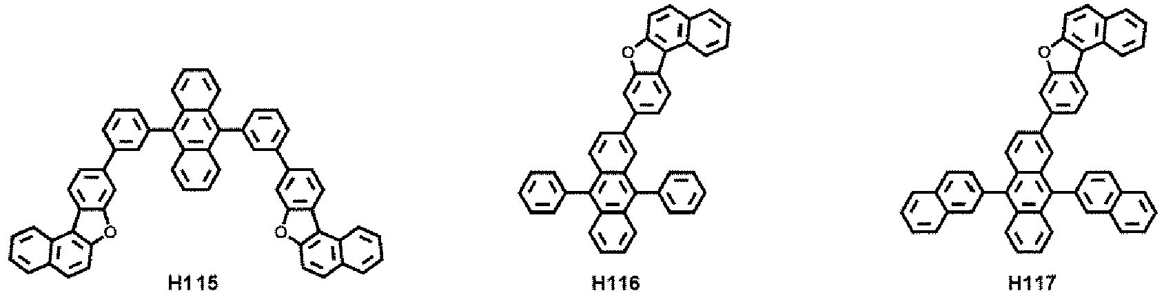


- The phosphorescent dopant may include the organometallic compound represented by Formula 1 described herein.
- The fluorescent dopant may include an amine group-containing compound, a styryl group-containing compound, or any combination thereof.
- In some embodiments, the fluorescent dopant may include a compound represented by Formula 501:

- Ar501, L501 to L503, R501, and R502 may each independently be a C3-C60 (e.g. C3-C30) carbocyclic group unsubstituted or substituted with at least one R10a or a C1-C60 (e.g. C1-C20) heterocyclic group unsubstituted or substituted with at least one R10a,
- xd1 to xd3 may each independently be 0, 1, 2, or 3, and
- xd4 may be 1, 2, 3, 4, 5, or 6.
- In some embodiments, in Formula 501, Ar501 may include a condensed ring group (e.g., an anthracene group, a chrysene group, or a pyrene group) in which at least three monocyclic groups are condensed.
- In some embodiments, xd4 in Formula 501 may be 2.
- In some embodiments, the fluorescent dopant may include one of Compounds FD1 to FD36, DPVBi, DPAVBi, or any combination thereof:
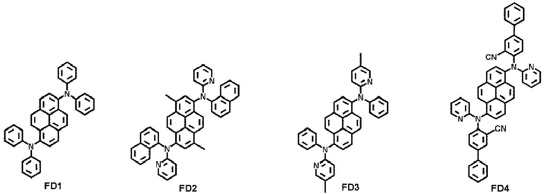


- The emission layer may include a delayed fluorescence material.
- The delayed fluorescence material described herein may be any suitable compound that may emit delayed fluorescence according to a delayed fluorescence emission mechanism.
- The delayed fluorescence material included in the emission layer may serve as a host or a dopant, depending on types (or kinds) of other materials included in the emission layer.
- In some embodiments, a difference between a triplet energy level (eV) of the delayed fluorescence material and a singlet energy level (eV) of the delayed fluorescence material may be about 0 eV or greater and about 0.5 eV or less. When the difference between a triplet energy level (eV) of the delayed fluorescence material and a singlet energy level (eV) of the delayed fluorescence material is within this range, up-conversion from a triplet state to a singlet state in the delayed fluorescence material may effectively (or suitably) occur, thus improving luminescence efficiency and/or the like of the light-emitting
device 10. - In some embodiments, the delayed fluorescence material may include: i) a material including at least one electron donor (e.g., a π electron-rich C3-C60 (e.g. C3-C30) cyclic group such as a carbazole group and/or the like) and at least one electron acceptor (e.g., a sulfoxide group, a cyano group, a π electron-deficient nitrogen-containing C1-C60 (e.g. C1-C30) cyclic group, and/or the like), ii) a material including a C8-C60 (e.g. C8-C30) polycyclic group including at least two cyclic groups condensed to each other and sharing boron (B), and/or the like.
- Examples of the delayed fluorescence material may include Compounds DF1 to DF9:


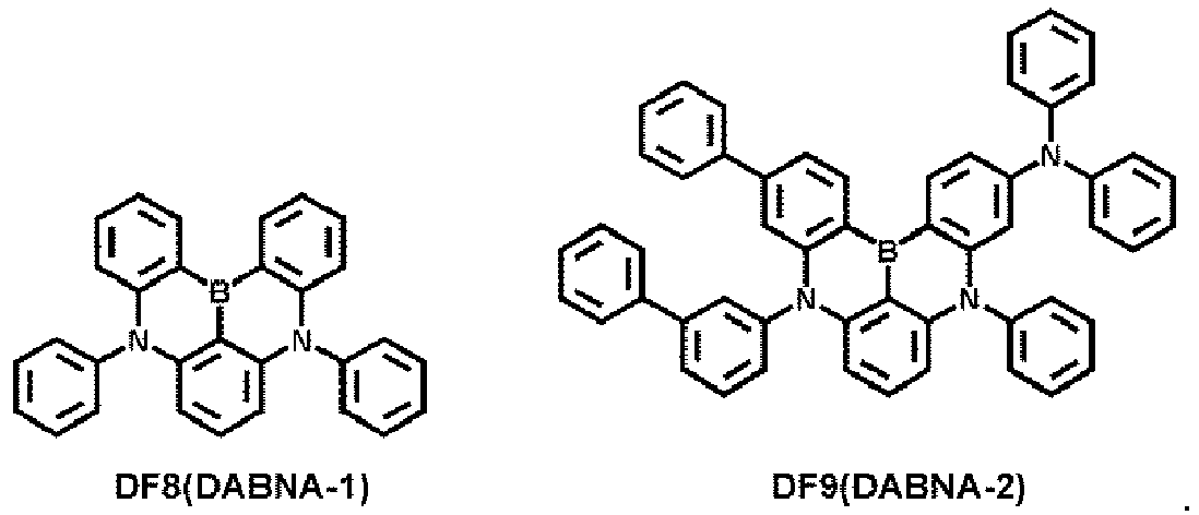
- The emission layer may include quantum dots.
- The term "quantum dot" as used herein refers to a crystal of a semiconductor compound and may include any suitable material capable of emitting a light of emission wavelengths of various lengths according to the size of the crystal.
- The diameter of the quantum dot may be, for example, in a range of about 1 nm to about 10 nm.
- Quantum dots may be synthesized by a wet chemical process, a metal organic chemical vapor deposition process, a molecular beam epitaxy process, or any similar suitable process.
- The wet chemical process is a method of growing a quantum dot particle crystal by mixing a precursor material with an organic solvent. When the crystal grows, the organic solvent may naturally serve as a dispersant coordinated on the surface of the quantum dot crystal and control the growth of the crystal. Thus, the wet chemical process may be easier than the vapor deposition process such as the metal organic chemical vapor deposition (MOCVD) process or the molecular beam epitaxy (MBE) process. Further, the growth of quantum dot particles may be controlled with a lower manufacturing cost.
- The quantum dot may include a group II-VI semiconductor compound; a group III-V semiconductor compound; a group III-VI semiconductor compound; a group I-III-VI semiconductor compound; a group IV-VI semiconductor compound; a group IV element, a group IV compound; or any combination thereof.
- Examples of the group II-VI semiconductor compound may include a binary compound such as CdS, CdSe, CdTe, ZnS, ZnSe, ZnTe, ZnO, HgS, HgSe, HgTe, MgSe, and/or MgS; a ternary compound such as CdSeS, CdSeTe, CdSTe, ZnSeS, ZnSeTe, ZnSTe, HgSeS, HgSeTe, HgSTe, CdZnS, CdZnSe, CdZnTe, CdHgS, CdHgSe, CdHgTe, HgZnS, HgZnSe, HgZnTe, MgZnSe, and/or MgZnS; a quaternary compound such as CdZnSeS, CdZnSeTe, CdZnSTe, CdHgSeS, CdHgSeTe, CdHgSTe, HgZnSeS, HgZnSeTe, and/or HgZnSTe; and any combination thereof.
- Examples of the group III-V semiconductor compound may include a binary compound such as GaN, GaP, GaAs, GaSb, AlN, AlP, AlAs, AlSb, InN, InP, InAs, and/or InSb; a ternary compound such as GaNP, GaNAs, GaNSb, GaPAs, GaPSb, AINP, AINAs, AINSb, AlPAs, AlPSb, InGaP, InNP, InAlP, InNAs, InNSb, InPAs, and/or InPSb; a quaternary compound such as GaAINP, GaAINAs, GaAINSb, GaAlPAs, GaAlPSb, GaInNP, GaInNAs, GaInNSb, GaInPAs, GaInPSb, InAINP, InAINAs, InAINSb, InAIPAs, and/or InAIPSb; and any combination thereof. In some embodiments, the group III-V semiconductor compound may further include a group II element. Examples of the group III-V semiconductor compound further including the group II element may include InZnP, InGaZnP, InAIZnP, and the like.
- Examples of the group III-VI semiconductor compound may include a binary compound such as GaS, GaSe, Ga2Se3, GaTe, InS, In2S3, InSe, In2Se3, InTe, and/or the like; a ternary compound such as InGaS3, InGaSe3, and/or the like; and any combination thereof.
- Examples of the group I-III-VI semiconductor compound may include a ternary compound such as AgInS, AgInS2, CuInS, CuInS2, CuGaO2, AgGaO2, AgAlO2, or any combination thereof.
- Examples of the group IV-VI semiconductor compound may include a binary compound such as SnS, SnSe, SnTe, PbS, PbSe, and/or PbTe; a ternary compound such as SnSeS, SnSeTe, SnSTe, PbSeS, PbSeTe, PbSTe, SnPbS, SnPbSe, and/or SnPbTe; a quaternary compound such as SnPbSSe, SnPbSeTe, and/or SnPbSTe; and any combination thereof.
- The group IV element and the group IV compound may be an elementary substance such as Si and/or Ge; a binary compound such as SiC and/or SiGe; or any combination thereof.
- Individual elements included in the multi-element compound, such as a binary compound, a ternary compound, and/or a quaternary compound, may be present in a particle thereof at a uniform or non-uniform concentration.
- The quantum dot may have a single structure in which the concentration of each element included in the quantum dot is uniform (or substantially uniform), or a core-shell double structure. In some embodiments, materials included in the core may be different from materials included in the shell.
- The shell of the quantum dot may serve as a protective layer for preventing or reducing chemical denaturation of the core to maintain semiconductor characteristics and/or as a charging layer for imparting electrophoretic characteristics to the quantum dot. The shell may be monolayer or multilayer. An interface between a core and a shell may have a concentration gradient where a concentration of elements present in the shell decreases toward the core.
- Examples of the shell of the quantum dot include a metal oxide, a nonmetal oxide, a semiconductor compound, and a combination thereof. Examples of the metal oxide and the nonmetal oxide may include: a binary compound such as SiO2, Al2O3, TiO2, ZnO, MnO, Mn2O3, Mn3O4, CuO, FeO, Fe2O3, Fe3O4, CoO, Co3O4, and/or NiO; a ternary compound such as MgAl2O4, CoFe2O4, NiFe2O4, and/or CoMn2O4; and any combination thereof. Examples of the semiconductor compound may include a group II-VI semiconductor compound; a group III-V semiconductor compound; a group III-VI semiconductor compound; a group I-III-VI semiconductor compound; a group IV-VI semiconductor compound; and any combination thereof. In some embodiments, the semiconductor compound may be CdS, CdSe, CdTe, ZnS, ZnSe, ZnTe, ZnSeS, ZnTeS, GaAs, GaP, GaSb, HgS, HgSe, HgTe, InAs, InP, InGaP, InSb, AlAs, AlP, AlSb, or any combination thereof.
- The quantum dot may have a full width of half maximum (FWHM) of a spectrum of an emission wavelength of about 45 nm or less, about 40 nm or less, or about 30 nm or less. When the FWHM of the quantum dot is within any of these ranges, color purity or color reproducibility may be improved. In addition, because light emitted through the quantum dot is emitted in all directions, an optical viewing angle may be improved.
- In one or more embodiments, the quantum dot may be, for example, a spherical, pyramidal, multi-arm, and/or cubic nanoparticle, nanotube, nanowire, nanofiber, and/or nanoplate.
- By adjusting the size of the quantum dot, the energy band gap may also be adjusted, thereby obtaining light of various wavelengths in the quantum dot emission layer. By using quantum dots of various sizes, a light-emitting device that may emit light of various wavelengths may be realized. In some embodiments, the size of the quantum dot may be selected such that the quantum dot may emit red, green, and/or blue light. In addition, the size of the quantum dot may be selected such that the quantum dot may emit white light by combining light of various colors.
- The electron transport region may have i) a single-layered structure including (e.g., consisting of) a single layer including (e.g., consisting of) a single material, ii) a single-layered structure including (e.g., consisting of) a single layer including a plurality of different materials, or iii) a multi-layered structure having a plurality of layers including a plurality of different materials.
- The electron transport region may include a buffer layer, a hole blocking layer, an electron control layer, an electron transport layer, and/or an electron injection layer.
- In some embodiments, the electron transport region may have an electron transport layer/electron injection layer structure, a hole blocking layer/electron transport layer/electron injection layer structure, an electron control layer/electron transport layer/electron injection layer structure, or a buffer layer/electron transport layer/electron injection layer structure, wherein the layers of each structure are sequentially stacked on the emission layer in each stated order.
- The electron transport region (e.g., a buffer layer, a hole blocking layer, an electron control layer, and/or an electron transport layer in the electron transport region) may include a metal-free compound including at least one π electron-deficient nitrogen-containing C1-C60 (e.g. C1-C30) cyclic group.
- In some embodiments, the electron transport region may include a compound represented by Formula 601:
Formula 601 [Ar601]xe11-[(L601)xe1-R601]xe21,
wherein, in Formula 601, - Ar601 and L601 may each independently be a C3-C60 (e.g. C3-C30) carbocyclic group unsubstituted or substituted with at least one R10a and/or a C1-C60 (e.g. C1-C20) heterocyclic group unsubstituted or substituted with at least one R10a,
- xe11 may be 1, 2, or 3,
- xe1 may be 0, 1, 2, 3, 4, or 5,
- R601 may be a C3-C60 (e.g. C3-C30) carbocyclic group unsubstituted or substituted with at least one R10a, a C1-C60 (e.g. C1-C20) heterocyclic group unsubstituted or substituted with at least one R10a, -Si(Q601)(Q602)(Q603), -C(=O)(Q601),-S(=O)2(Q601), and/or -P(=O)(Q601)(Q602),
- Q601 to Q603 may each be understood by referring to the description of Q1 provided herein,
- xe21 may be 1, 2, 3, 4, or 5, and
- at least one of Ar601, L601, and R601 may each independently be a π electron-deficient nitrogen-containing C1-C60 (e.g. C1-C30) cyclic group unsubstituted or substituted with at least one R10a.
- In some embodiments, when xe11 in Formula 601 is 2 or greater, at least two Ar601(s) may be bound via a single bond.
- In some embodiments, in Formula 601, Ar601 may be a substituted or unsubstituted anthracene group.
- In some embodiments, the electron transport region may include a compound represented by Formula 601-1:

- X614 may be N or C(R614), X615 may be N or C(R615), X616 may be N or C(R616), and at least one selected from X614 to X616 may be N,
- L611 to L613 may each be understood by referring to the description of L601 provided herein,
- xe611 to xe613 may each be understood by referring to the description of xe1 provided herein,
- R611 to R613 may each be understood by referring to the description of R601 provided herein, and
- R614 to R616 may each independently be hydrogen, deuterium, -F, -Cl, -Br, -I, a hydroxyl group, a cyano group, a nitro group, a C1-C20 (e.g. C1-C10) alkyl group, a C1-C20 (e.g. C1-C10) alkoxy group, a C3-C60 (e.g. C3-C30) carbocyclic group unsubstituted or substituted with at least one R10a, and/or a C1-C60 (e.g. C1-C20) heterocyclic group unsubstituted or substituted with at least one R10a.
- For example, in Formulae 601 and 601-1, xe1 and xe611 to xe613 may each independently be 0, 1, or 2.
- The electron transport region may include one of Compounds ET1 to ET45, 2,9-dimethyl-4,7-diphenyl-1,10-phenanthroline (BCP), 4,7-diphenyl-1,10-phenanthroline (Bphen), Alq3, BAlq, TAZ, NTAZ, or any combination thereof:


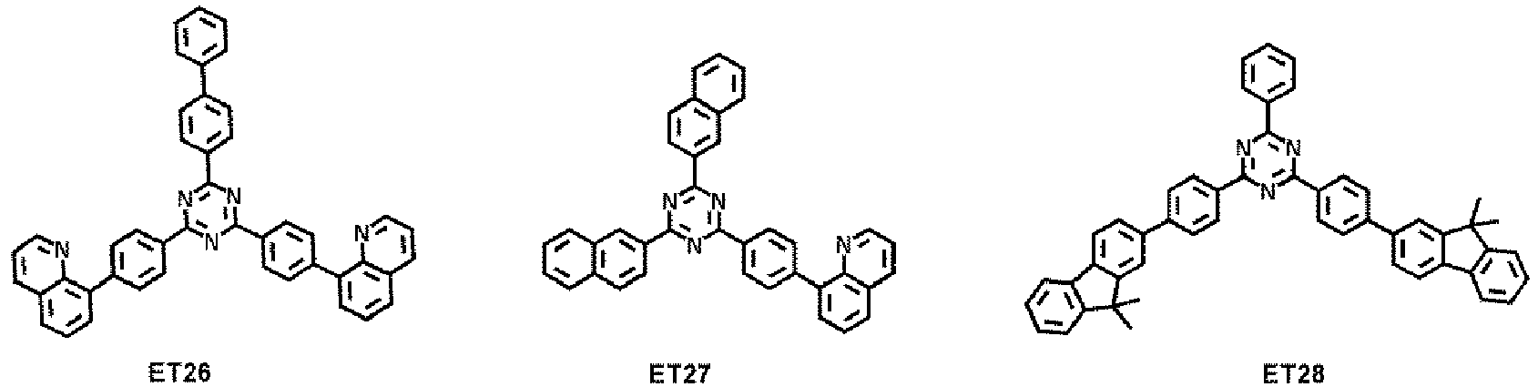


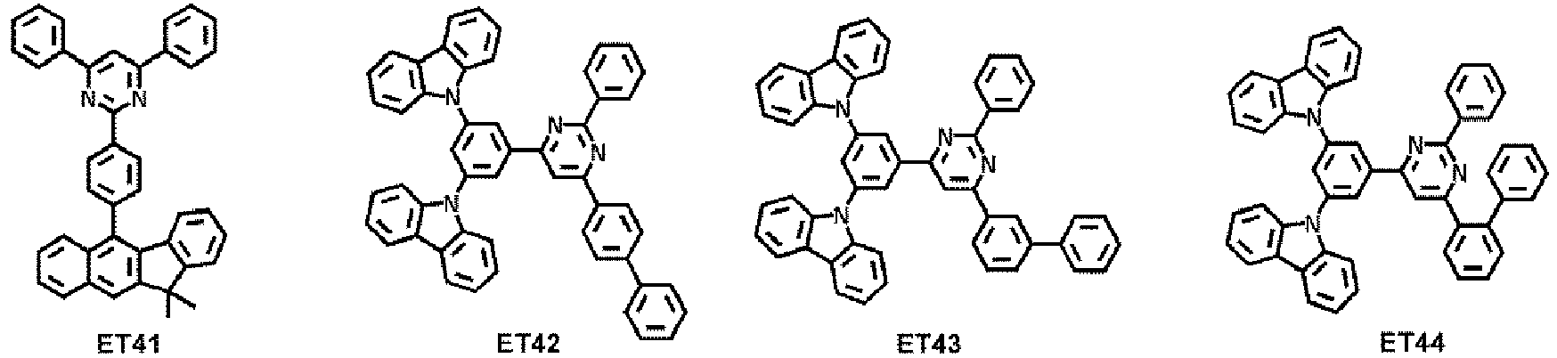


- The thickness of the electron transport region may be in a range of about 50 Angstroms (Å) to about 5,000 Å, for example, about 100 Å to about 4,000 Å or about 100 Å to about 1,000 Å. When the electron transport region includes a buffer layer, a hole blocking layer, an electron control layer, an electron transport layer, or any combination thereof, the thicknesses of the buffer layer, the hole blocking layer, or the electron control layer may each independently be in a range of about 20 Å to about 1,000 Å, for example, about 20 Å to about 700 Å, about 20 Å to about 500 Å, about 20 Å to about 400 Å, about 30 Å to about 400 Å or about 30 Å to about 300 Å, and the thickness of the electron transport layer may be in a range of about 100 Å to about 1,000 Å, for example, about 100 Å to about 700 Å, about 100 Å to about 600 Å, about 150 Å to about 600 Å, about 150 Å to about 500 Å or about 300 Å to about 500 Å. When the thicknesses of the buffer layer, the hole blocking layer, the electron control layer, the electron transport layer, and/or the electron transport region are each within these ranges, excellent (or improved) electron transport characteristics may be obtained without a substantial increase in driving voltage.
- The electron transport region (for example, the electron transport layer in the electron transport region) may further include, in addition to the materials described above, a metal-containing material.
- The metal-containing material may include an alkali metal complex, an alkaline earth metal complex, or any combination thereof. A metal ion of the alkali metal complex may be a lithium (Li) ion, a sodium (Na) ion, a potassium (K) ion, a rubidium (Rb) ion, and/or a cesium (Cs) ion. A metal ion of the alkaline earth metal complex may be a beryllium (Be) ion, a magnesium (Mg) ion, a calcium (Ca) ion, a strontium (Sr) ion, and/or a barium (Ba) ion. A ligand coordinated with the metal ion of the alkali metal complex and the alkaline earth metal complex may each independently be hydroxyquinoline, hydroxyisoquinoline, hydroxybenzoquinoline, hydroxyacridine, hydroxyphenanthridine, hydroxyphenyloxazole, hydroxyphenylthiazole, hydroxyphenyloxadiazole, hydroxyphenylthiadiazole, hydroxyphenylpyridine, hydroxyphenylbenzimidazole, hydroxyphenylbenzothiazole, bipyridine, phenanthroline, cyclopentadiene, or any combination thereof.
- For example, the metal-containing material may include a Li complex. The Li complex may include, e.g., Compound ET-D1 (LiQ) and/or Compound ET-D2:

- The electron transport region may include an electron injection layer that facilitates injection of electrons from the
second electrode 150. The electron injection layer may be in direct contact with thesecond electrode 150. - The electron injection layer may have i) a single-layered structure including (e.g., consisting of) a single layer including (e.g., consisting of) a single material, ii) a single-layered structure including (e.g., consisting of) a single layer including a plurality of different materials, or iii) a multi-layered structure having a plurality of layers including a plurality of different materials.
- The electron injection layer may include an alkali metal, an alkaline earth metal, a rare earth metal, an alkali metal-containing compound, an alkaline earth metal-containing compound, a rare earth metal-containing compound, an alkali metal complex, an alkaline earth metal complex, a rare earth metal complex, or any combination thereof.
- The alkali metal may be Li, Na, K, Rb, Cs or any combination thereof. The alkaline earth metal may be Mg, Ca, Sr, Ba, or any combination thereof. The rare earth metal may be Sc, Y, Ce, Tb, Yb, Gd, or any combination thereof.
- The alkali metal-containing compound, the alkaline earth metal-containing compound, and the rare earth metal-containing compound may each independently be oxides, halides (e.g., fluorides, chlorides, bromides, and/or iodides), tellurides, or any combination thereof of the alkali metal, the alkaline earth metal, and the rare earth metal, respectively.
- The alkali metal-containing compound may be alkali metal oxides (such as Li2O, Cs2O, and/or K2O), alkali metal halides (such as LiF, NaF, CsF, KF, Lil, Nal, Csl, and/or KI), or any combination thereof. The alkaline earth-metal-containing compound may include alkaline earth-metal oxides, such as BaO, SrO, CaO, BaxSr1-xO (wherein x is a real number satisfying 0<x<1), and/or BaxCa1-xO (wherein x is a real number satisfying 0<x<1). The rare earth metal-containing compound may include YbF3, ScF3, Sc2O3, Y2O3, Ce2O3, GdF3, TbF3, YbI3, ScI3, TbI3, or any combination thereof. In some embodiments, the rare earth metal-containing compound may include a lanthanide metal telluride. Examples of the lanthanide metal telluride may include LaTe, CeTe, PrTe, NdTe, PmTe, SmTe, EuTe, GdTe, TbTe, DyTe, HoTe, ErTe, TmTe, YbTe, LuTe, La2Te3, Ce2Te3, Pr2Te3, Nd2Te3, Pm2Te3, Sm2Te3, Eu2Te3, Gd2Te3, Tb2Te3, Dy2Te3, Ho2Te3, Er2Te3, Tm2Te3, Yb2Te3, Lu2Te3, and the like.
- The alkali metal complex, the alkaline earth metal complex, and the rare earth metal complex may include: i) one of ions of the alkali metal, alkaline earth metal, and rare earth metal described above, respectively, and ii) a ligand bound to the metal ion, e.g., hydroxyquinoline, hydroxyisoquinoline, hydroxybenzoquinoline, hydroxyacridine, hydroxyphenanthridine, hydroxyphenyloxazole, hydroxyphenylthiazole, hydroxyphenyloxadiazole, hydroxyphenylthiadiazole, hydroxyphenylpyridine, hydroxyphenylbenzimidazole, hydroxyphenylbenzothiazole, bipyridine, phenanthroline, cyclopentadiene, or any combination thereof.
- The electron injection layer may include (e.g., may consist of) an alkali metal, an alkaline earth metal, a rare earth metal, an alkali metal-containing compound, an alkaline earth metal-containing compound, a rare earth metal-containing compound, an alkali metal complex, an alkaline earth metal complex, a rare earth metal complex, or any combination thereof, as described above. In some embodiments, the electron injection layer may further include an organic material (e.g., a compound represented by Formula 601).
- In some embodiments, the electron injection layer may include (e.g., may consist of) i) an alkali metal-containing compound (e.g., alkali metal halide), or ii) a) an alkali metal-containing compound (e.g., alkali metal halide); and b) an alkali metal, an alkaline earth metal, a rare earth metal, or any combination thereof. In some embodiments, the electron injection layer may be a KI:Yb co-deposition layer, a RbI:Yb co-deposition layer, and/or the like.
- When the electron injection layer further includes an organic material, the alkali metal, the alkaline earth metal, the rare earth metal, the alkali metal-containing compound, the alkaline earth metal-containing compound, the rare earth metal-containing compound, the alkali metal complex, the alkaline earth metal complex, the rare earth metal complex, or any combination thereof may be homogeneously or non-homogeneously dispersed in a matrix including the organic material.
- The thickness of the electron injection layer may be in a range of about 1 Å to about 100 Å, and in some embodiments, about 3 Å to about 90 Å or about 3 Å to about 20 Å. When the thickness of the electron injection layer is within any of these ranges, excellent (or improved) electron injection characteristics may be obtained without a substantial increase in driving voltage.
- The
second electrode 150 is on theinterlayer 130. In one or more embodiments, thesecond electrode 150 may be a cathode that is an electron injection electrode. In this embodiment, a material for forming thesecond electrode 150 may be a material having a low work function, for example, a metal, an alloy, an electrically conductive compound, or any combination thereof. - The
second electrode 150 may include lithium (Li), silver (Ag), magnesium (Mg), aluminum (Al), aluminum-lithium (Al-Li), calcium (Ca), magnesium-indium (Mg-In), magnesium-silver (Mg-Ag), ytterbium (Yb), silver-ytterbium (Ag-Yb), ITO, IZO, or any combination thereof. Thesecond electrode 150 may be a transmissive electrode, a semi-transmissive electrode, or a reflective electrode. - The
second electrode 150 may have a single-layered structure, or a multi-layered structure including two or more layers. - A first capping layer may be located outside the
first electrode 110, and/or a second capping layer may be located outside thesecond electrode 150. In some embodiments, the light-emittingdevice 10 may have a structure in which the first capping layer, thefirst electrode 110, theinterlayer 130, and thesecond electrode 150 are sequentially stacked in this stated order, a structure in which thefirst electrode 110, theinterlayer 130, thesecond electrode 150, and the second capping layer are sequentially stacked in this stated order, or a structure in which the first capping layer, thefirst electrode 110, theinterlayer 130, thesecond electrode 150, and the second capping layer are sequentially stacked in this stated order. - In the light-emitting
device 10, light emitted from the emission layer in theinterlayer 130 may pass through the first electrode 110 (which may be a semi-transmissive electrode or a transmissive electrode) and through the first capping layer to the outside, and/or may pass through the second electrode 150 (which may be a semi-transmissive electrode or a transmissive electrode) and through the second capping layer to the outside. - The first capping layer and the second capping layer may improve the external luminescence efficiency based on the principle of constructive interference. Accordingly, the optical extraction efficiency of the light-emitting
device 10 may be increased, thus improving luminescence efficiency of the light-emittingdevice 10. - The first capping layer and the second capping layer may each include a material having a refractive index of about 1.6 or higher (at 589 nm).
- The first capping layer and the second capping layer may each independently be an organic capping layer including an organic material, an inorganic capping layer including an inorganic material, and/or a composite capping layer including an organic material and an inorganic material.
- At least one of the first capping layer and the second capping layer may each independently include carbocyclic compound(s), heterocyclic compound(s), amine group-containing compound(s), porphine derivative(s), phthalocyanine derivative(s), naphthalocyanine derivative(s), alkali metal complex(es), alkaline earth metal complex(es), or any combination thereof. The carbocyclic compound, the heterocyclic compound, and the amine group-containing compound may each independently be optionally substituted with a substituent of O, N, S, Se, Si, F, Cl, Br, I, or any combination thereof. In some embodiments, at least one of the first capping layer and the second capping layer may each independently include an amine group-containing compound.
- In some embodiments, at least one of the first capping layer and the second capping layer may each independently include the compound represented by Formula 201, the compound represented by Formula 202, or any combination thereof.
- In one or more embodiments, at least one of the first capping layer and the second capping layer may each independently include one of Compounds HT28 to HT33, one of Compounds CP1 to CP6, β-NPB, or any combination thereof:


- The light-emitting device may be included in one or more suitable electronic apparatuses. In some embodiments, an electronic apparatus including the light-emitting device may be an emission apparatus and/or an authentication apparatus.
- The electronic apparatus (e.g., an emission apparatus) may further include, in addition to the light-emitting device, i) a color filter, ii) a color-conversion layer, or iii) a color filter and a color-conversion layer. The color filter and/or the color-conversion layer may be disposed (e.g., positioned) in at least one traveling direction of light emitted from the light-emitting device. For example, light emitted from the light-emitting device may be blue light or white light. The light-emitting device may be understood by referring to the descriptions provided herein. In some embodiments, the color-conversion layer may include quantum dots. The quantum dot may be, for example, the quantum dot described herein.
- The electronic apparatus may include a first substrate. The first substrate may include a plurality of sub-pixel areas, the color filter may include a plurality of color filter areas respectively corresponding to the plurality of sub-pixel areas, and the color-conversion layer may include a plurality of color-conversion areas respectively corresponding to the plurality of sub-pixel areas.
- A pixel defining film may be located between the plurality of sub-pixel areas to define each sub-pixel area.
- The color filter may further include a plurality of color filter areas and light-blocking patterns between the plurality of color filter areas, and the color-conversion layer may further include a plurality of color-conversion areas and light-blocking patterns between the plurality of color-conversion areas.
- The plurality of color filter areas (or the plurality of color-conversion areas) may include: a first area emitting (e.g., to emit) first color light; a second area emitting (e.g., to emit) second color light; and/or a third area emitting (e.g., to emit) third color light, and the first color light, the second color light, and/or the third color light may have different maximum emission wavelengths. In some embodiments, the first color light may be red light, the second color light may be green light, and the third color light may be blue light. In some embodiments, the plurality of color filter areas (or the plurality of color-conversion areas) may include quantum dots. In some embodiments, the first area may include red quantum dots, the second area may include green quantum dots, and the third area may not include a quantum dot. The quantum dot may be understood by referring to the description of the quantum dot provided herein. The first area, the second area, and/or the third area may further include a scatterer.
- In some embodiments, the light-emitting device may emit first light, the first area may absorb the first light to emit 1-1 color light, the second area may absorb the first light to emit 2-1 color light, and the third area may absorb the first light to emit 3-1 color light. In this embodiment, the 1-1 color light, the 2-1 color light, and the 3-1 color light may each have a different maximum emission wavelength. In some embodiments, the first light may be blue light, the 1-1 color light may be red light, the 2-1 color light may be green light, and the 3-1 light may be blue light.
- The electronic apparatus may further include a thin-film transistor, in addition to the light-emitting device. The thin-film transistor may include a source electrode, a drain electrode, and an active layer, wherein one of the source electrode and the drain electrode may be electrically connected (e.g., electrically coupled) to one of the first electrode and the second electrode of the light-emitting device.
- The thin-film transistor may further include a gate electrode, a gate insulating film, and/or the like.
- The active layer may include a crystalline silicon, an amorphous silicon, an organic semiconductor, and/or an oxide semiconductor.
- The electronic apparatus may further include an encapsulation unit for sealing the light-emitting device. The encapsulation unit may be located between the color filter and/or the color-conversion layer and the light-emitting device. The encapsulation unit may allow light to pass to the outside from the light-emitting device, and may at the same time (e.g., concurrently) prevent or reduce the permeation of air and moisture into the light-emitting device. The encapsulation unit may be a sealing substrate including a transparent glass and/or a plastic substrate. The encapsulation unit may be a thin-film encapsulating layer including at least one organic layer and/or at least one inorganic layer. When the encapsulation unit is a thin film encapsulating layer, the electronic apparatus may be flexible.
- In addition to the color filter and/or the color-conversion layer, various functional layers may be disposed (e.g., provided) on the encapsulation unit depending on the use of an electronic apparatus. Examples of the functional layer may include a touch screen layer, a polarization layer, and the like. The touch screen layer may be a resistive touch screen layer, a capacitive touch screen layer, and/or an infrared beam touch screen layer. The authentication apparatus may be, for example, a biometric authentication apparatus that identifies an individual according biometric information (e.g., a fingertip, a pupil, and/or the like).
- The authentication apparatus may further include a biometric information collecting unit, in addition to the light-emitting device described above.
- The electronic apparatus may be applicable to various suitable displays, an optical source, lighting, a personal computer (e.g., a mobile personal computer), a cellphone, a digital camera, an electronic note, an electronic dictionary, an electronic game console, a medical device (e.g., an electronic thermometer, a blood pressure meter, a glucometer, a pulse measuring device, a pulse wave measuring device, an electrocardiograph recorder, an ultrasonic diagnosis device, an endoscope display device), a fish finder, various measurement devices, gauges (e.g., gauges of an automobile, an airplane, a ship), a projector, without limitation.
-
FIG. 2 is a schematic cross-sectional view of a light-emitting apparatus according to one or more embodiments. - A light-emitting apparatus in
FIG. 2 may include asubstrate 100, a thin-film transistor, a light-emitting device, and anencapsulation unit 300 sealing the light-emitting device. - The
substrate 100 may be a flexible substrate, a glass substrate, and/or a metal substrate. Abuffer layer 210 may be on thesubstrate 100. Thebuffer layer 210 may prevent or reduce penetration of impurities through thesubstrate 100, and may provide a flat surface on thesubstrate 100. - A thin-film transistor may be on the
buffer layer 210. The thin-film transistor may include anactive layer 220, agate electrode 240, asource electrode 260, and adrain electrode 270. - The
active layer 220 may include an inorganic semiconductor such as silicon and/or polysilicon, an organic semiconductor, and/or an oxide semiconductor, and may include a source area, a drain area, and a channel area. - A
gate insulating film 230 for insulating theactive layer 220 and thegate electrode 240 may be on theactive layer 220, and thegate electrode 240 may be on thegate insulating film 230. - An interlayer insulating
film 250 may be on thegate electrode 240. Theinterlayer insulating film 250 may be between thegate electrode 240 and thesource electrode 260 and between thegate electrode 240 and thedrain electrode 270 to provide insulation therebetween. - The
source electrode 260 and thedrain electrode 270 may be on theinterlayer insulating film 250. Theinterlayer insulating film 250 and thegate insulating film 230 may be formed to expose the source area and the drain area of theactive layer 220, and thesource electrode 260 and thedrain electrode 270 may be adjacent to the exposed source area and the exposed drain area of theactive layer 220. - Such a thin-film transistor may be electrically connected (e.g., electrically coupled) to a light-emitting device to drive the light-emitting device and may be protected by a
passivation layer 280. Thepassivation layer 280 may include an inorganic insulating film, an organic insulating film, or a combination thereof. A light-emitting device may be on thepassivation layer 280. The light-emitting device includes afirst electrode 110, aninterlayer 130, and asecond electrode 150. - The
first electrode 110 may be on thepassivation layer 280. Thepassivation layer 280 may not fully cover thedrain electrode 270 and may expose a specific or set area of thedrain electrode 270, and thefirst electrode 110 may be disposed to connect (e.g., to electrically couple) to the exposeddrain electrode 270. - A pixel-defining
film 290 may be on thefirst electrode 110. The pixel-definingfilm 290 may expose a specific or set area of thefirst electrode 110, and theinterlayer 130 may be formed in the exposed area. The pixel-definingfilm 290 may include one or more suitable organic insulating materials, inorganic insulating materials, and/or organic/inorganic composite insulating materials. In some embodiments, the pixel-definingfilm 290 may be a polyimide and/or a polyacryl organic film. In one or more embodiments, some or more layers of theinterlayer 130 may extend to the upper portion of the pixel-definingfilm 290 and may be disposed in the form of a common layer. - The
second electrode 150 may be on theinterlayer 130, and acapping layer 170 may be additionally formed on thesecond electrode 150. Thecapping layer 170 may be formed to cover thesecond electrode 150. - The
encapsulation unit 300 may be on thecapping layer 170. Theencapsulation unit 300 may be on the light-emitting device to protect a light-emitting device from moisture and/or oxygen. Theencapsulation unit 300 may include: an inorganic film including silicon nitride (SiNx), silicon oxide (SiOx), indium tin oxide, indium zinc oxide, or any combination thereof; an organic film including polyethylene terephthalate, polyethylene naphthalate, polycarbonate, polyimide, polyethylene sulfonate, polyoxy methylene, polyaryllate, hexamethyl disiloxane, an acrylic resin (e.g., polymethyl methacrylate, polyacrylic acid, and/or the like), an epoxy resin (e.g., aliphatic glycidyl ether (AGE) and/or the like), or any combination thereof; or a combination of the inorganic film and the organic film. -
FIG. 3 is a schematic cross-sectional view of another light-emitting apparatus according to one or more embodiments. - The emission apparatus (e.g., the light-emitting apparatus) shown in
FIG. 3 may be substantially identical to the emission apparatus (e.g., the light-emitting apparatus) shown inFIG. 2 , except that a light-shielding pattern 500 and afunctional area 400 are additionally located on theencapsulation unit 300. Thefunctional area 400 may be i) a color filter area, ii) a color-conversion area, or iii) a combination of a color filter area and a color-conversion area. In some embodiments, the light-emitting device shown inFIG. 3 included in the emission apparatus may be a tandem light-emitting device. - The layers constituting the hole transport region, the emission layer, and the layers constituting the electron transport region may each independently be formed in a set or specific region by using one or more suitable methods such as vacuum deposition, spin coating, casting, Langmuir-Blodgett (LB) deposition, ink-jet printing, laser printing, and/or laser-induced thermal imaging.
- When layers constituting the hole transport region, the emission layer, and layers constituting the electron transport region are each independently formed by vacuum-deposition, the vacuum-deposition may be performed at a deposition temperature in a range of about 100 °C to about 500 °C, at a vacuum degree in a range of about 10-8 torr to about 10-3 torr, and at a deposition rate in a range of about 0.01 Angstroms per second (Å/sec) to about 100 Å/sec, depending on the material to be included in each layer and the structure of each layer to be formed.
- The term "C3-C60 carbocyclic group" as used herein refers to a cyclic group consisting of carbon atoms only and having 3 to 60 carbon atoms. The term "C1-C60 heterocyclic group" as used herein refers to a cyclic group having 1 to 60 carbon atoms, in addition to a heteroatom other than carbon atoms. The C3-C60 carbocyclic group and the C1-C60 heterocyclic group may each independently be a monocyclic group consisting of one ring or a polycyclic group in which at least two rings are condensed. For example, the number of ring-forming atoms in the C1-C60 heterocyclic group may be in a range of 3 to 61.
- The term "cyclic group" as used herein may include the C3-C60 carbocyclic group and the C1-C60 heterocyclic group.
- The term "π electron-rich C3-C60 cyclic group" refers to a cyclic group having 3 to 60 carbon atoms and not including *-N=*' as a ring-forming moiety. The term "π electron-deficient nitrogen-containing C1-C60 cyclic group" as used herein refers to a heterocyclic group having 1 to 60 carbon atoms and *-N=*' as a ring-forming moiety.
- In some embodiments,
- the C3-C60 carbocyclic group may be i) a T1 group or ii) a group in which at least two T1 groups are condensed (for example, the C3-C60 carbocyclic group may be a cyclopentadiene group, an adamantane group, a norbornane group, a benzene group, a pentalene group, a naphthalene group, an azulene group, an indacene group, an acenaphthylene group, a phenalene group, a phenanthrene group, an anthracene group, a fluoranthene group, a triphenylene group, a pyrene group, a chrysene group, a perylene group, a pentaphene group, a heptalene group, a naphthacene group, a picene group, a hexacene group, a pentacene group, a rubicene group, a coronene group, an ovalene group, an indene group, a fluorene group, a spiro-bifluorene group, a benzofluorene group, an indenophenanthrene group, and/or an indenoanthracene group),
- the C1-C60 heterocyclic group may be i) a T2 group, ii) a group in which at least two T2 groups are condensed, or iii) a group in which at least one T2 group is condensed with at least one T1 group (for example, the C1-C60 heterocyclic group may be a pyrrole group, a thiophene group, a furan group, an indole group, a benzoindole group, a naphthoindole group, an isoindole group, a benzoisoindole group, a naphthoisoindole group, a benzosilole group, a benzothiophene group, a benzofuran group, a carbazole group, a dibenzosilole group, a dibenzothiophene group, a dibenzofuran group, an indenocarbazole group, an indolocarbazole group, a benzofurocarbazole group, a benzothienocarbazole group, a benzosilolocarbazole group, a benzoindolocarbazole group, a benzocarbazole group, a benzonaphthofuran group, a benzonapthothiophene group, a benzonaphthosilole group, a benzofurodibenzofuran group, a benzofurodibenzothiophene group, a benzothienodibenzothiophene group, a pyrazole group, an imidazole group, a triazole group, an oxazole group, an isoxazole group, an oxadiazole group, a thiazole group, an isothiazole group, a thiadiazole group, a benzopyrazole group, a benzimidazole group, a benzoxazole group, a benzoisoxazole group, a benzothiazole group, a benzoisothiazole group, a pyridine group, a pyrimidine group, a pyrazine group, a pyridazine group, a triazine group, a quinoline group, an isoquinoline group, a benzoquinoline group, a benzoisoquinoline group, a quinoxaline group, a benzoquinoxaline group, a quinazoline group, a benzoquinazoline group, a phenanthroline group, a cinnoline group, a phthalazine group, a naphthyridine group, an imidazopyridine group, an imidazopyrimidine group, an imidazotriazine group, an imidazopyrazine group, an imidazopyridazine group, an azacarbazole group, an azafluorene group, an azadibenzosilole group, an azadibenzothiophene group, an azadibenzofuran group, and/or the like),
- the π electron-rich C3-C60 cyclic group may be i) a T1 group, ii) a condensed group in which at least two T1 groups are condensed, iii) a T3 group, iv) a condensed group in which at least two T3 groups are condensed, or v) a condensed group in which at least one T3 group is condensed with at least one T1 group (for example, the π electron-rich C3-C60 cyclic group may be a C3-C60 carbocyclic group, a pyrrole group, a thiophene group, a furan group, an indole group, a benzoindole group, a naphthoindole group, an isoindole group, a benzoisoindole group, a naphthoisoindole group, a benzosilole group, a benzothiophene group, a benzofuran group, a carbazole group, a dibenzosilole group, a dibenzothiophene group, a dibenzofuran group, an indenocarbazole group, an indolocarbazole group, a benzofurocarbazole group, a benzothienocarbazole group, a benzosilolocarbazole group, a benzoindolocarbazole group, a benzocarbazole group, a benzonaphthofuran group, a benzonapthothiophene group, a benzonaphthosilole group, a benzofurodibenzofuran group, a benzofurodibenzothiophene group, a benzothienodibenzothiophene group, and/or the like), and
- the π electron-deficient nitrogen-containing C1-C60 cyclic group may be i) a T4 group, ii) a group in which at least twos T4 groups are condensed, iii) a group in which at least one T4 group is condensed with at least one T1 group, iv) a group in which at least one T4 group is condensed with at least one T3 group, or v) a group in which at least one T4 group, at least one T1 group, and at least one T3 group are condensed (for example, the π electron-deficient nitrogen-containing C1-C60 cyclic group may be a pyrazole group, an imidazole group, a triazole group, an oxazole group, an isoxazole group, an oxadiazole group, a thiazole group, an isothiazole group, a thiadiazole group, a benzopyrazole group, a benzimidazole group, a benzoxazole group, a benzoisoxazole group, a benzothiazole group, a benzoisothiazole group, a pyridine group, a pyrimidine group, a pyrazine group, a pyridazine group, a triazine group, a quinoline group, an isoquinoline group, a benzoquinoline group, a benzoisoquinoline group, a quinoxaline group, a benzoquinoxaline group, a quinazoline group, a benzoquinazoline group, a phenanthroline group, a cinnoline group, a phthalazine group, a naphthyridine group, an imidazopyridine group, an imidazopyrimidine group, an imidazotriazine group, an imidazopyrazine group, an imidazopyridazine group, an azacarbazole group, an azafluorene group, an azadibenzosilole group, an azadibenzothiophene group, an azadibenzofuran group, and/or the like),
- wherein the T1 group may be a cyclopropane group, a cyclobutane group, a cyclopentane group, a cyclohexane group, a cycloheptane group, a cyclooctane group, a cyclobutene group, a cyclopentene group, a cyclopentadiene group, a cyclohexene group, a cyclohexadiene group, a cycloheptene group, an adamantane group, a norbornane (or bicyclo[2.2.1]heptane) group, a norbornene group, a bicyclo[1.1.1]pentane group, a bicyclo[2.1.1]hexane group, a bicyclo[2.2.2]octane group, and/or a benzene group,
- the T2 group may be a furan group, a thiophene group, a 1H-pyrrole group, a silole group, a borole group, a 2H-pyrrole group, a 3H-pyrrole group, an imidazole group, a pyrazole group, a triazole group, a tetrazole group, an oxazole group, an isoxazole group, an oxadiazole group, a thiazole group, an isothiazole group, a thiadiazole group, an azasilole group, an azaborole group, a pyridine group, a pyrimidine group, a pyrazine group, a pyridazine group, a triazine group, and/or a tetrazine group,
- the T3 group may be a furan group, a thiophene group, a 1H-pyrrole group, a silole group, and/or a borole group, and
- the T4 group may be a 2H-pyrrole group, a 3H-pyrrole group, an imidazole group, a pyrazole group, a triazole group, a tetrazole group, an oxazole group, an isoxazole group, an oxadiazole group, a thiazole group, an isothiazole group, a thiadiazole group, an azasilole group, an azaborole group, a pyridine group, a pyrimidine group, a pyrazine group, a pyridazine group, a triazine group, and/or a tetrazine group.
- The "cyclic group", "C3-C60 carbocyclic group", "C1-C60 heterocyclic group", "π electron-rich C3-C60 cyclic group", and/or "π electron-deficient nitrogen-containing C1-C60 cyclic group" as used herein may each independently be a group condensed with any suitable cyclic group, a monovalent group, and/or a polyvalent group (e.g., a divalent group, a trivalent group, a quadvalent group, or the like), depending on the structure of the formula to which the respective term is applied. For example, a "benzene group" may be a benzo group, a phenyl group, a phenylene group, and/or the like, and this may be understood by one of ordinary skill in the art, depending on the structure of the formula including the "benzene group".
- Examples of the monovalent C3-C60 carbocyclic group and the monovalent C1-C60 heterocyclic group may include a C3-C10 cycloalkyl group, a C1-C10 heterocycloalkyl group, a C3-C10 cycloalkenyl group, a C1-C10 heterocycloalkenyl group, a C6-C60 aryl group, a C1-C60 heteroaryl group, a monovalent non-aromatic condensed polycyclic group, and a monovalent non-aromatic condensed heteropolycyclic group. Examples of the divalent C3-C60 carbocyclic group and the divalent C1-C60 heterocyclic group may include a C3-C10 cycloalkylene group, a C1-C10 heterocycloalkylene group, a C3-C10 cycloalkenylene group, a C1-C10 heterocycloalkenylene group, a C6-C60 arylene group, a C1-C60 heteroarylene group, a divalent non-aromatic condensed polycyclic group, and a divalent non-aromatic condensed heteropolycyclic group.
- The term "C1-C60 alkyl group" as used herein refers to a linear or branched aliphatic saturated hydrocarbon monovalent group having 1 to 60 carbon atoms, and examples thereof include a methyl group, an ethyl group, an n-propyl group, an isopropyl group, an n-butyl group, a sec-butyl group, an isobutyl group, a tert-butyl group, an n-pentyl group, a tert-pentyl group, a neopentyl group, an isopentyl group, a sec-pentyl group, a 3-pentyl group, a sec-isopentyl group, an n-hexyl group, an iso-hexyl group, a sec-hexyl group, a tert-hexyl group, an n-heptyl group, an iso-heptyl group, a sec-heptyl group, a tert-heptyl group, an n-octyl group, an iso-octyl group, a sec-octyl group, a tert-octyl group, an n-nonyl group, an iso-nonyl group, a sec-nonyl group, a tert-nonyl group, an n-decyl group, an iso-decyl group, a sec-decyl group, and a tert-decyl group. The term "C1-C60 alkylene group" as used herein refers to a divalent group having the same structure as the C1-C60 alkyl group. Corresponding definitions apply to other ranges given for the number of carbon atoms in an alkyl/alkylene group.
- The term "C2-C60 alkenyl group" as used herein refers to a monovalent hydrocarbon group having at least one carbon-carbon double bond in the middle and/or at either terminus of the C2-C60 alkyl group. Examples thereof include an ethenyl group, a propenyl group, and a butenyl group. The term "C2-C60 alkenylene group" as used herein refers to a divalent group having the same structure as the C2-C60 alkenyl group. Corresponding definitions apply to other ranges given for the number of carbon atoms in an alkenyl/alkenylene group.
- The term "C2-C60 alkynyl group" as used herein refers to a monovalent hydrocarbon group having at least one carbon-carbon triple bond in the middle and/or at either terminus of the C2-C60 alkyl group. Examples thereof include an ethynyl group and a propynyl group. The term "C2-C60 alkynylene group" as used herein refers to a divalent group having the same structure as the C2-C60 alkynyl group. Corresponding definitions apply to other ranges given for the number of carbon atoms in an alkynyl/alkynylene group.
- The term "C1-C60 alkoxy group" as used herein refers to a monovalent group represented by -OA101 (wherein A101 is the C1-C60 alkyl group). Examples thereof include a methoxy group, an ethoxy group, and an isopropyloxy group. Corresponding definitions apply to other ranges given for the number of carbon atoms in an alkoxy group.
- The term "C3-C10 cycloalkyl group" as used herein refers to a monovalent saturated hydrocarbon monocyclic group including 3 to 10 carbon atoms. Examples of the C3-C10 cycloalkyl group as used herein include a cyclopropyl group, a cyclobutyl group, a cyclopentyl group, a cyclohexyl group, a cycloheptyl group, a cyclooctyl group, an adamantyl group, a norbornyl (bicyclo[2.2.1]heptyl) group, a bicyclo[1.1.1]pentyl group, a bicyclo[2.1.1]hexyl group, and a bicyclo[2.2.2]octyl group. The term "C3-C10 cycloalkylene group" as used herein refers to a divalent group having the same structure as the C3-C10 cycloalkyl group.
- The term "C1-C10 heterocycloalkyl group" as used herein refers to a monovalent cyclic group including at least one heteroatom other than carbon atoms as a ring-forming atom and having 1 to 10 carbon atoms. Examples thereof include a 1,2,3,4-oxatriazolidinyl group, a tetrahydrofuranyl group, and a tetrahydrothiophenyl group. The term "C1-C10 heterocycloalkylene group" as used herein refers to a divalent group having the same structure as the C1-C10 heterocycloalkyl group.
- The term "C3-C16 cycloalkenyl group" as used herein refers to a monovalent cyclic group that has 3 to 10 carbon atoms and at least one carbon-carbon double bond in its ring, and is not aromatic. Examples thereof include a cyclopentenyl group, a cyclohexenyl group, and a cycloheptenyl group. The term "C3-C10 cycloalkenylene group" as used herein refers to a divalent group having the same structure as the C3-C10 cycloalkenyl group.
- The term "C1-C10 heterocycloalkenyl group" as used herein refers to a monovalent cyclic group including at least one heteroatom other than carbon atoms as a ring-forming atom, 1 to 10 carbon atoms, and at least one double bond in its ring. Examples of the C1-C10 heterocycloalkenyl group include a 4,5-dihydro-1,2,3,4-oxatriazolyl group, a 2,3-dihydrofuranyl group, and a 2,3-dihydrothiophenyl group. The term "C1-C10 heterocycloalkylene group" as used herein refers to a divalent group having the same structure as the C1-C10 heterocycloalkenyl group.
- The term "C6-C60 aryl group" as used herein refers to a monovalent group having a carbocyclic aromatic system having 6 to 60 carbon atoms. Examples of the C6-C60 aryl group include a phenyl group, a pentalenyl group, a naphthyl group, an azulenyl group, an indacenyl group, an acenaphthyl group, a phenalenyl group, a phenanthrenyl group, an anthracenyl group, a fluoranthenyl group, a triphenylenyl group, a pyrenyl group, a chrysenyl group, a perylenyl group, a pentaphenyl group, a heptalenyl group, a naphthacenyl group, a picenyl group, a hexacenyl group, a pentacenyl group, a rubicenyl group, a coronenyl group, and an ovalenyl group. The term "C6-C60 arylene group" as used herein refers to a divalent group having the same structure as the C6-C60 aryl group. When the C6-C60 aryl group and the C6-C60 arylene group each independently include two or more rings, the respective rings may be fused. Corresponding definitions apply to other ranges given for the number of carbon atoms in an aryl/arylene group.
- The term "C1-C60 heteroaryl group" as used herein refers to a monovalent group having a heterocyclic aromatic system further including at least one heteroatom other than carbon atoms as a ring-forming atom and 1 to 60 carbon atoms. Examples of the C1-C60 heteroaryl group include a pyridinyl group, a pyrimidinyl group, a pyrazinyl group, a pyridazinyl group, a triazinyl group, a quinolinyl group, a benzoquinolinyl group, an isoquinolinyl group, a benzoisoquinolinyl group, a quinoxalinyl group, a benzoquinoxalinyl group, a quinazolinyl group, a benzoquinazolinyl group, a cinnolinyl group, a phenanthrolinyl group, a phthalazinyl group, and a naphthyridinyl group. The term "C1-C60 heteroarylene group" as used herein refers to a divalent group having the same structure as the C1-C60 heteroaryl group. When the C1-C60 heteroaryl group and the C1-C60 heteroarylene group each independently include two or more rings, the respective rings may be fused. Corresponding definitions apply to other ranges given for the number of carbon atoms in an heteroaryl/heteroarylene group.
- The term "monovalent non-aromatic condensed polycyclic group" as used herein refers to a monovalent group that has two or more rings condensed and only carbon atoms (e.g., 8 to 60 carbon atoms) as ring forming atoms, wherein the molecular structure when considered as a whole is non-aromatic. Examples of the monovalent non-aromatic condensed polycyclic group include an indenyl group, a fluorenyl group, a spiro-bifluorenyl group, a benzofluorenyl group, an indenophenanthrenyl group, and an indenoanthracenyl group. The term "divalent non-aromatic condensed polycyclic group" as used herein refers to a divalent group having substantially the same structure as the monovalent non-aromatic condensed polycyclic group.
- The term "monovalent non-aromatic condensed heteropolycyclic group" as used herein refers to a monovalent group that has two or more condensed rings and at least one heteroatom other than carbon atoms (e.g., 1 to 60 carbon atoms), as a ring-forming atom, wherein the molecular structure when considered as a whole is non-aromatic. Examples of the monovalent non-aromatic condensed heteropolycyclic group include a 9,10-dihydroacridinyl group and a 9H-xanthenyl group. The term "divalent non-aromatic condensed heteropolycyclic group" as used herein refers to a divalent group having substantially the same structure as the monovalent non-aromatic condensed heteropolycyclic group.
- The term "C6-C60 aryloxy group" as used herein refers to a monovalent group represented by -OA102 (wherein A102 is the C6-C60 aryl group). The term "C6-C60 arylthio group" as used herein refers to a monovalent group represented by -SA103 (wherein A103 is the C6-C60 aryl group). Corresponding definitions apply to other ranges given for the number of carbon atoms in an aryloxy group and an arylthio group.
- The term "R10a" as used herein may be:
- deuterium (-D), -F, -Cl, -Br, -I, a hydroxyl group, a cyano group, or a nitro group;
- a C1-C60 (e.g. C1-C20) alkyl group, a C2-C60 (e.g. C2-C20) alkenyl group, a C2-C60 (e.g. C2-C20) alkynyl group, or a C1-C60 (e.g. C1-C20) alkoxy group, each unsubstituted or substituted with deuterium, -F, -CI, -Br, -I, a hydroxyl group, a cyano group, a nitro group, a C3-C60 (e.g. C3-C30) carbocyclic group, a C1-C60 (e.g. C1-C20) heterocyclic group, a C6-C60 (e.g. C6-C30) aryloxy group, a C6-C60 (e.g. C6-C30) arylthio group, -Si(Q11)(Q12)(Q13), -N(Q11)(Q12), -B(Q11)(Q12), -C(=O)(Q11), -S(=O)2(Q11), - P(=O)(Q11)(Q12), or any combination thereof;
- a C3-C60 (e.g. C3-C30) carbocyclic group, a C1-C60 (e.g. C1-C20) heterocyclic group, a C6-C60 (e.g. C6-C30) aryloxy group, or a C6-C60 (e.g. C6-C30) arylthio group, each unsubstituted or substituted with deuterium, -F, -CI, -Br, -I, a hydroxyl group, a cyano group, a nitro group, a C1-C60 (e.g. C1-C20) alkyl group, a C2-C60 (e.g. C2-C20) alkenyl group, a C2-C60 (e.g. C2-C20) alkynyl group, a C1-C60 (e.g. C1-C20) alkoxy group, a C3-C60 (e.g. C3-C30) carbocyclic group, a C1-C60 (e.g. C1-C20) heterocyclic group, a C6-C60 (e.g. C6-C30) aryloxy group, a C6-C60 (e.g. C6-C30) arylthio group, - Si(Q21)(Q22)(Q23), -N(Q21)(Q22), -B(Q21)(Q22), -C(=O)(Q21), -S(=O)2(Q21), - P(=O)(Q21)(Q22), or any combination thereof; or
- -Si(Q31)(Q32)(Q33), -N(Q31)(Q32), -B(Q31)(Q32), -C(=O)(Q31), -S(=O)2(Q31), or - P(=O)(Q31)(Q32).
- Q1 to Q3, Q11 to Q13, Q21 to Q23, and Q31 to Q33 may each independently be hydrogen; deuterium; -F; -CI; -Br; -I; a hydroxyl group; a cyano group; a nitro group; a C1-C60 (e.g. C1-C20) alkyl group; a C2-C60 (e.g. C2-C20) alkenyl group; a C2-C60 (e.g. C2-C20) alkynyl group; a C1-C60 (e.g. C1-C20) alkoxy group; or a C3-C60 (e.g. C3-C30) carbocyclic group or a C1-C60 (e.g. C1-C20) heterocyclic group, each unsubstituted or substituted with deuterium, -F, a cyano group, a C1-C60 (e.g. C1-C20) alkyl group, a C1-C60 (e.g. C1-C20) alkoxy group, a phenyl group, a biphenyl group, or any combination thereof.
- The term "heteroatom" as used herein refers to any atom other than a carbon atom. Examples of the heteroatom may include O, S, N, P, Si, B, Ge, Se, and any combination thereof.
- "Ph" used herein represents a phenyl group, "Me" used herein represents a methyl group, "Et" used herein represents an ethyl group, "t-Bu", "tertBu", "tert-Bu" or "But" used herein represents a tert-butyl group, and "OMe" used herein represents a methoxy group.
- The term "biphenyl group" as used herein may refer to a phenyl group substituted with a phenyl group. For example, the "biphenyl group" may be "a substituted phenyl group" having a "C6-C60 aryl group" as a substituent.
- The term "terphenyl group" as used herein may refer to a phenyl group substituted with biphenyl group. For example, the "terphenyl group" may be "a substituted phenyl group" having a "C6-C60 aryl group substituted with a C6-C60 aryl group" as a substituent.
- The symbols *, *' and *" as used herein, unless defined otherwise, refer to a binding site to an adjacent atom in a corresponding formula.
- Hereinafter, compounds and a light-emitting device according to one or more embodiments will be described in more detail with reference to Synthesis Examples and Examples. The wording "B was used instead of A" used in describing Synthesis Examples means that an amount of B used was identical to an amount of A used in terms of molar equivalents.
- Compounds 1 to 6 used in the Synthesis Examples are as follows:

- 11.5 grams (g) of 2,6-dibromoaniline (Compound 1) (45.7 millimole (mmol)), 1.1 g of Pd(PPh3)4 (0.9 mmol), K2CO3 (137.1 mmol), and 8.7 g of [1,2]azaborinino[1,2-a][1,2]azaborinin-1-ylboronic acid (50.3 mmol) were added to a reaction vessel, and suspended in 300 milliliters (mL) of toluene and 100 mL of H2O, followed by heating at a temperature of 100 °C for 6 hours. Once the reaction was complete, the temperature was lowered to room temperature, and 300 mL of distilled water was added thereto. Then, an organic layer was extracted therefrom using ethyl acetate, and the extracted organic layer was washed with saturated NaCl aqueous solution, followed by drying using sodium sulfate. The resulting product was subjected to column chromatography to thereby obtain 11.9 g (34.3 mmol) of Intermediate IM-1-1 (yield: 75 %).
- 13.5 g of Intermediate IM-1-2 (33.4 mmol) was synthesized in substantially the same manner as in Synthesis of Intermediate IM-1-1, except that 2,6-dibromo-4-(tert-butyl)aniline (Compound 2) was used instead of 2,6-dibromoaniline (Compound 1) (yield: 73 %).
- 11.9 g of Intermediate IM-1 -1 (34.3 mmol), 9.4 g of 1 -iodo-2-nitrobenzene (37.7 mmol), 0.6 g of Pd2(dba)3 (0.69 mmol), 0.6 g of SPhos (1.37 mmol), and 5.3 g of NaO tert Bu(NaOtBu) (54.9 mmol) were added to a reaction vessel and suspended in 343 mL of toluene, followed by heating at a temperature of 120 °C for 4 hours. Once the reaction was complete, the temperature was lowered to room temperature, and 300 mL of distilled water was added thereto. Then, an organic layer was extracted therefrom using ethyl acetate, and the extracted organic layer was washed with saturated NaCl aqueous solution, followed by drying using sodium sulfate. The resulting product was subjected to column chromatography to thereby obtain 12.5 g (26.8 mmol) of Intermediate IM-2-1 (yield: 78 %).
- 13.1 g of Intermediate IM-2-2 (25.0 mmol) was synthesized in substantially the same manner as in Synthesis of Intermediate IM-2-1, except that Intermediate IM-1-2 was used instead of Intermediate IM-1-1 (yield: 73 %).
- 12.5 g of Intermediate IM-2-1 (26.8 mmol) and 3.2 g of Sn (26.8 mmol) were added to a reaction vessel and suspended in 268 mL of ethanol, followed by adding 3.2 mL of HCl (37 %) dropwise thereto and heating at 80 °C for 10 hours. Once the reaction was complete, the temperature was lowered to room temperature, and 300 mL of distilled water was added thereto. Then, an organic layer was extracted therefrom using ethyl acetate, and the extracted organic layer was washed with saturated NaCl aqueous solution, followed by drying using sodium sulfate. The resulting product was subjected to column chromatography to thereby obtain 9.4 g (21.4 mmol) of Intermediate IM-3-1 (yield: 80 %).
- 10.3 g of Intermediate IM-3-2 (20.9 mmol) was synthesized in substantially the same manner as in Synthesis of Intermediate IM-3-1, except that Intermediate IM-2-2 was used instead of Intermediate IM-2-1 (yield: 78%).

- 5.0 g of Intermediate IM-3-1 (11.4 mmol), 6.1 g of 2-(3-bromo-5-(tert-butyl)phenoxy)-9-(4-(tert-butyl)pyridin-2-yl)-9H-carbazole-5,6,7,8-d 4 (Compound 3) (11.4 mmol), 0.2 g of Pd2(dba)3 (0.2 mmol), 1.9 g of SPhos (4.6 mmol), and 1.7 g of NaO tert Bu (18.2 mmol) were added to a reaction vessel and suspended in 114 mL of toluene, followed by heating at a temperature of 120 °C for 4 hours. Once the reaction was complete, the temperature was lowered to room temperature, and 300 mL of distilled water was added thereto. Then, an organic layer was extracted therefrom using ethyl acetate, and the extracted organic layer was washed with saturated NaCl aqueous solution, followed by drying using sodium sulfate. The resulting product was subjected to column chromatography to thereby obtain 7.6 g (8.6 mmol) of Intermediate IM-4-1 (yield: 75 %).
- 7.8 g of Intermediate IM-4-2 (8.3 mmol) was synthesized in substantially the same manner as in Synthesis of Intermediate IM-4-1, except that Intermediate IM-3-2 was used instead of Intermediate IM-3-1 (yield: 73 %).
- 13.5 g of Intermediate IM-4-3 (15.2 mmol) was synthesized in substantially the same manner as in Synthesis of Intermediate IM-4-2, except that 2-(3-bromophenoxy)-9-(4-(tert-butyl)pyridin-2-yl)-9H-carbazole-5,6,7,8-d 4 (Compound 4), instead of Compound 3, was reacted with Intermediate IM-3-2 (yield: 75 %).
- 8.2 g of Intermediate IM-4-4 (8.4 mmol) was synthesized in substantially the same manner as in Synthesis of Intermediate IM-4-3, except that 2-((5-bromo-[1,1'-biphenyl]-3-yl-2',3',4',5',6'-d5)oxy)-9-(4-(tert-butyl)py-ridin-2-yl)-9H-carbazole-5,6,7,8-d 4 (Compound 5), instead of Compound 4, was reacted with Intermediate IM-3-2 (yield: 74 %).
- 8.4 g of Intermediate IM-4-5 (7.8 mmol) was synthesized in substantially the same manner as in Synthesis of Intermediate IM-4-4, except that 2-((5-bromo-2',4',6'-tri-tert-butyl-[1,1'-biphenyl]-3-yl)oxy)-9-(4-(tert-butyl)-pyridin-2-yl)-9H-carbazole-5,6,7,8-d4 (Compound 6), instead of Compound 5, was reacted with Intermediate IM-3-1, instead of Intermediate IM-3-2 (yield: 68 %).
- 8.4 g of Intermediate IM-4-6 (7.4 mmol) was synthesized in substantially the same manner as in Synthesis of Intermediate IM-4-5, except that 2-((5-bromo-2',4',6'-tri-tert-butyl-[1,1'-biphenyl]-3-yl)oxy)-9-(4-(tert-butyl)-pyridin-2-yl) -9H-carbazole-5,6,7,8-d 4 (Compound 6) was reacted with Intermediate IM-3-2 instead of Intermediate IM-3-1 (yield: 65 %).

- 7.6 g of Intermediate IM-4-1 (8.6 mmol), 86 mL of triethyl orthoformate (516 mmol), and 1.0 mL of HCl (37 %) (10.3 mmol) were added to a reaction vessel, followed by heating at a temperature of 80 °C for 12 hours. Once the reaction was complete, the temperature was cooled to room temperature, and the resulting solid was filtered and washed using ether. Then, the washed solid was dried to thereby obtain 7.2 g (7.7 mmol) of Intermediate IM-5-1 at a yield of 90 %.
- 7.3 g of Intermediate IM-5-2 (7.4 mmol), 6.9 g of Intermediate IM-5-3 (7.4 mmol), 7.4 g of Intermediate IM-5-4 (7.3 mmol), 8.0 g of Intermediate IM-5-5 (7.1 mmol), and 8.4 g of Intermediate IM-5-6 (7.1 mmol) were respectively synthesized in substantially the same manner as in Synthesis of Intermediate IM-5-1, except that Intermediate IM-4-2, Intermediate IM-4-3, Intermediate IM-4-4, Intermediate IM-4-5, and Intermediate IM-4-6 were respectively used instead of Intermediate IM-4-1, at a yield of 86 %, 86 %, 85 %, 83 %, and 82 %, respectively.

- 7.2 g of Intermediate IM-5-1 (7.7 mmol) and 3.8 g of NH4PF6 (23.1 mmol) were added to a reaction vessel, followed by suspension in a mixture solution of 100 mL of methanol and 50 mL of water and stirring at room temperature for 24 hours. Once the reaction was complete, the resulting solid was filtered and washed using ether. Then, the washed solid was dried to thereby obtain 7.0 g (6.9 mmol) of Intermediate IM-6-1 at a yield of 90 %.
- 7.6 g of Intermediate IM-6-2 (6.9 mmol), 6.9 g of Intermediate IM-6-3 (6.8 mmol), 8.0 g of Intermediate IM-6-4 (7.1 mmol), 8.5 g of Intermediate IM-6-5 (6.9 mmol), and 8.8 g of Intermediate IM-6-6 (6.8 mmol) were respectively synthesized in substantially the same manner as in Synthesis of Intermediate IM-6-1, except that Intermediate IM-5-2, Intermediate IM-5-3, Intermediate IM-5-4, Intermediate IM-5-5, and Intermediate IM-5-6 were respectively used instead of Intermediate IM-5-1, at a yield of 90 % 88 % 92 % 90 % and 89 % respectively.

-

- 7.0 g of Intermediate IM-6-1 (6.9 mmol), 2.8 g of dichloro(1,5-cyclooctadiene)platinum (7.6 mmol), and 1.7 g of NaOAc (20.7 mmol) were suspended in 150 mL of 1,4-dioxane, followed by heating at a temperature of 110 °C for 72 hours. Once the reaction was complete, the temperature was cooled to room temperature, 150 mL of distilled water was added thereto, and an organic layer was extracted therefrom using ethyl acetate, and the extracted organic layer was washed using NaCl aqueous solution and dried using MgSO4. The resulting product was subjected to column chromatography to thereby obtain 2.6 g (2.4 mmol) of Compound BD04 (yield: 35 %).
-

- 2.8 g of Compound BD19 (2.4 mmol) was synthesized in substantially the same manner as in Synthesis of Compound BD04, except that Intermediate IM-6-2 was used instead of Intermediate IM-6-1 (yield: 35 %).
-
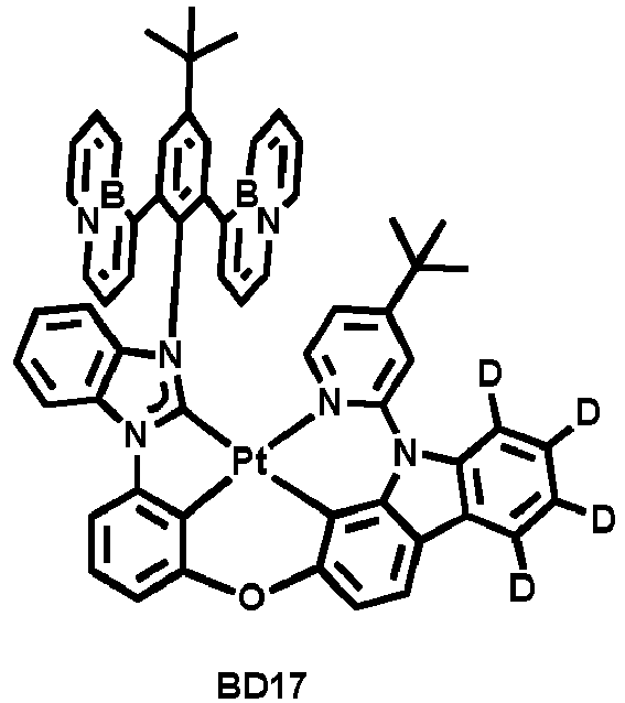
- 2.4 g of Compound BD17 (2.2 mmol) was synthesized in substantially the same manner as in Synthesis of Compound BD04, except that Intermediate IM-6-3 was used instead of Intermediate IM-6-1 (yield: 32 %).
-
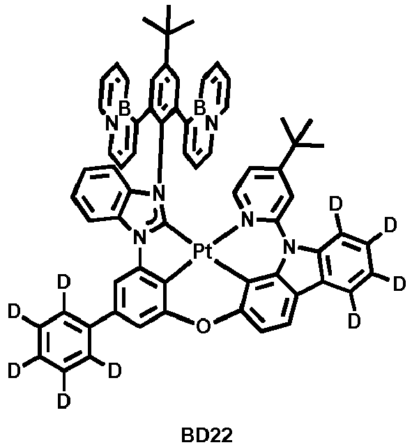
- 2.9 g of Compound BD22 (2.5 mmol) was synthesized in substantially the same manner as in Synthesis of Compound BD04, except that Intermediate IM-6-4 was used instead of Intermediate IM-6-1 (yield: 36 %).
-

- 2.9 g of Compound BD10 (2.3 mmol) was synthesized in substantially the same manner as in Synthesis of Compound BD04, except that Intermediate IM-6-5 was used instead of Intermediate IM-6-1 (yield: 34 %).
-

- 3.2 g of Compound BD25 (2.4 mmol) was synthesized in substantially the same manner as in Synthesis of Compound BD04, except that Intermediate IM-6-6 was used instead of Intermediate IM-6-1 (yield: 35 %).
- Compounds synthesized in Synthesis Examples 17 to 22 were identified by 1H nuclear magnetic resonance (NMR) and matrix-assisted laser desorption/ionization mass spectrometry time-of-flight mass spectroscopy (MALDI-TOF MS). The results thereof are shown in Table 1.
- Methods of synthesizing compounds other than the compounds synthesized in Synthesis Examples 17 to 22 may be easily understood by those skilled in the art by referring to the synthesis pathways and raw materials described above.
Table 1 Compo und 1H NMR (CDCl3, 500 MHz) MALDI-TOF MS [M+| found calc. BD04 δ 9.01 (d, 3JH-H = 6.3 Hz, 1H), 8.08 (s, 1H), 7.86 (d, 3JH-H = 8.3 Hz, 1H), 7.64 (d, 3JH-H = 8.3 Hz, 1H), 7.60-7.40 (m, 3H), 7.32 (d, 3JH-H = 8.2 Hz, 1H), 7.24-7.22 (m, 3H), 7.15-7.00 (m, 2H), 6.89 (d, 3JH-H = 8.2 Hz, 1H), 6.86-6.65 (m, 7H), 6.37 (dd, 3JH-H = 8.1 Hz, 2H), 6.19 (dd, 3JH-H = 6.3 Hz, 4JH-H = 1.7 Hz, 1H), 6.16 (dd, 3JH-H = 8.1 Hz, 2H), 5.32 (dd, 3JH-H = 8.1 Hz, 2H), 1.42 (s, 9H), 1.29 (s, 9H). 1091.41 34 1091.41 31 BD19 δ 9.03 (d, 3JH-H = 6.3 Hz, 1H), 8.01 (s, 1H), 7.86 (d, 3JH-H = 8.3 Hz, 1H), 7.64 (d, 3JH-H = 8.3 Hz, 1H), 7.60-7.40 (m, 2H), 7.32 (d, 3JH-H = 8.2 Hz, 1H), 7.24-7.22 (m, 3H), 7.15-7.00 (m, 2H), 6.89 (d, 3JH-H = 8.2 Hz, 1H), 6.86-6.65 (m, 7H), 6.37 (dd, 3JH-H = 8.1 Hz, 2H), 6.19 (dd, 3JH-H = 6.3 Hz, 4JH-H = 1.7 Hz, 1H), 6.16 (dd, 3JH-H = 8.1 Hz, 2H), 5.32 (dd, 3JH-H = 8.1 Hz, 2H), 1.42 (s, 9H), 1.31 (s, 9H), 1.29 (s, 9H). 1147.47 61 1147.47 57 BD17 δ 9.10 (d, 3JH-H = 6.3 Hz, 1H), 8.12 (s, 1H), 7.88 (d, 3JH-H = 8.3 Hz, 1H), 7.63 (d, 3JH-H = 8.3 Hz, 1H), 7.62-7.41 (m, 3H), 7.31 (d, 3JH-H = 8.2 Hz, 1H), 7.24-7.22 (m, 3H), 7.16-7.01 (m, 2H), 6.87 (d, 3JH-H = 8.2 Hz, 1H), 6.86-6.65 (m, 7H), 6.36 (dd, 3JH-H = 8.1 Hz, 2H), 6.18 (dd, 3JH-H = 6.3 Hz, 4JH-H = 1.7 Hz, 1H), 6.15 (dd, 3JH-H = 8.1 Hz, 2H), 5.34 (dd, 3JH-H = 8.1 Hz, 2H), 1.31 (s, 9H), 1.29 (s, 9H). 1091.41 36 1091.41 31 BD22 δ 9.00 (d, 3JH-H = 6.3 Hz, 1H), 8.03 (s, 1H), 7.87 (d, 3JH-H = 8.3 Hz, 1H), 7.65 (d, 3JH-H = 8.3 Hz, 1H), 7.58-7.38 (m, 2H), 7.30 (d, 3JH-H = 8.2 Hz, 1H), 7.26-7.23 (m, 3H), 7.16-7.01 (m, 2H), 6.87 (d, 3JH-H = 8.2 Hz, 1H), 6.87-6.64 (m, 7H), 6.36 (dd, 3JH-H = 8.1 Hz, 2H), 6.18 (dd, 3JH-H = 6.3 Hz, 4JH-H = 1.7 Hz, 1H), 6.14 (dd, 3JH-H = 8.1 Hz, 2H), 5.31 (dd, 3JH-H = 8.1 Hz, 2H), 1.42 (s, 9H), 1.30 (s, 9H). 1172.47 63 1172.47 58 BD10 δ 9.01 (d, 3JH-H = 6.3 Hz, 1H), 8.08 (s, 1H), 7.84 (d, 3JH-H = 8.3 Hz, 1H), 7.64 (d, 3JH-H = 8.3 Hz, 1H), 7.60-7.41 (m, 2H), 7.29 (d, 3JH-H = 8.2 Hz, 1H), 7.28-7.21 (m, 4H), 7.16-7.00 (m, 4H), 6.89 (d, 3JH-H = 8.2 Hz, 1H), 6.85-6.63 (m, 7H), 6.33 (dd, 3JH-H = 8.1 Hz, 2H), 6.18 (dd, 3JH-H = 6.3 Hz, 4JH-H = 1.7 Hz, 1H), 6.12 (dd, 3JH-H = 8.1 Hz, 2H), 5.26 (dd, 3JH-H = 8.1 Hz, 2H), 1.35 (s, 18H), 1.31 (s, 9H), 1.30 (s, 9H). 1279.57 01 1279.56 96 BD25 δ 9.12 (d, 3JH-H = 6.3 Hz, 1H), 8.02 (s, 1H), 7.86 (d, 3JH-H = 8.3 Hz, 1H), 7.64 (d, 3JH-H = 8.3 Hz, 1H), 7.60-7.41 (m, 2H), 7.29 (d, 3JH-H = 8.2 Hz, 1H), 7.27-7.22 (m, 3H), 7.16-7.00 (m, 4H), 6.88 (d, 3JH-H = 8.2 Hz, 1H), 6.86-6.64 (m, 7H), 6.32 (dd, 3JH-H = 8.1 Hz, 2H), 6.17 (dd, 3JH-H = 6.3 Hz, 4JH-H = 1.7 Hz, 1H), 6.11 (dd, 3JH-H = 8.1 Hz, 2H), 5.28 (dd, 3JH-H = 8.1 Hz, 2H), 1.42 (s, 9H), 1.35 (s, 18H), 1.31 (s, 9H), 1.30 (s, 9H). 1335.63 25 1335.63 22 - A Corning 15 Ohms per square centimeter (Ω/cm2) (1,200 Å) ITO glass substrate was cut to a size of 50 millimeters (mm)×50 mm×0.7 mm, sonicated in isopropyl alcohol and pure water for 5 minutes in each solvent, and cleaned by exposure to ultraviolet rays with ozone to use the glass substrate as an anode. Then, the glass substrate was mounted onto a vacuum-deposition apparatus. 2-TNATA was vacuum-deposited on the glass substrate to form a hole injection layer having a thickness of 600 Å. Then, 4,4'-bis[N-(1-naphthyl)-N-phenylamino]biphenyl (NPB) was vacuum-deposited on the hole injection layer to form a hole transport layer having a thickness of about 300 Å. Compound ETH1 and Compound HTH15 were mixed at a weight ratio of 3:7 as a mixture host to be deposited on the hole transport layer, Compound BD04 was used as a dopant (dopant 13 wt%), and ETH1, HTH15, and BD04 were co-deposited to form an emission layer to a thickness of 400 Å. Subsequently, HBL-1 was vacuum-deposited to a thickness of 50 Å to form a hole blocking layer. Alq3 was deposited on the hole blocking layer as an electron transport layer to a thickness of 300 Å, LiF was deposited on the electron transport layer to a thickness of 10 Å as an electron injection layer, Al was vacuum-deposited to a thickness of 3,000 Å to form a LiF/AI cathode, thereby completing the manufacture of a light-emitting device.


- A light-emitting device was manufactured in substantially the same manner as in Example 1, except that ETH2 and HTH15 were used as a mixture host at a weight ratio of 3:7 to form an emission layer.
- A light-emitting device was manufactured in substantially the same manner as in Example 1, except that ETH2 and HTH15 were used as a mixture host at a weight ratio of 3:7 to form an emission layer, and BD19 was used instead of BD04.
- A light-emitting device was manufactured in substantially the same manner as in Example 1, except that ETH2 and HTH15 were used as a mixture host at a weight ratio of 3:7 to form an emission layer, and BD17 was used instead of BD04.
- A light-emitting device was manufactured in substantially the same manner as in Example 1, except that ETH2 and HTH15 were used as a mixture host at a weight ratio of 3:7 to form an emission layer, and BD22 was used instead of BD04.
- A light-emitting device was manufactured in substantially the same manner as in Example 1, except that ETH2 and HTH15 were used as a mixture host at a weight ratio of 3:7 to form an emission layer, and BD10 was used instead of BD04.
- A light-emitting device was manufactured in substantially the same manner as in Example 1, except that ETH2 and HTH15 were used as a mixture host at a weight ratio of 3:7 to form an emission layer, and BD25 was used instead of BD04.
- A light-emitting device was manufactured in substantially the same manner as in Example 1, except that ETH2 and HTH15 were mixed as a mixture host at a weight ratio of 3:7 to form an emission layer, and BD17 (13 wt%) and a delayed fluorescence dopant DFD7 (0.4 wt%), instead of BD04, were co-deposited to form an emission layer having a thickness of 400 Å.
- A light-emitting device was manufactured in substantially the same manner as in Example 1, except that Compound BD-CE1 was used instead of Compound BD04 to form an emission layer.

- A light-emitting device was manufactured in substantially the same manner as in Example 1, except that Compound BD-CE2 was used instead of Compound BD04 to form an emission layer.

- A light-emitting device was manufactured in substantially the same manner as in Example 1, except that Compound BD-CE3 was used instead of Compound BD04 to form an emission layer.

- A light-emitting device was manufactured in substantially the same manner as in Example 1, except that Compound BD-CE4 was used instead of Compound BD04 to form an emission layer.

- The driving voltage, color coordinates, luminescence efficiency, color-conversion efficiency (luminescence efficiency/CIEy), maximum emission wavelength (nm), and lifespan (T95) at luminance of 1,000 cd/m2 of the light-emitting devices manufactured in Examples 1 to 8 and Comparative Examples 1 to 4 were measured by using Keithley source-measure unit (SMU) 236 and a luminance meter PR650. The results thereof are shown in Table 2. In Table 2, the lifespan (T95) indicates a time (in hours) that it took for the luminance of each light-emitting device to decline to 95 % of its initial luminance under the same condition.
Table 2 Luminance (cd/m2) Driving voltage (V) CIE(x,y) Luminescence efficiency (cd/A) Color-conversion efficiency (cd/A/y) Maximum emission wavelength (nm) Lifespan (T95, hour) Example 1 1,000 4.9 (0.134, 0.181) 22.1 122.3 462 121.0 Example 2 1,000 4.9 (0.134, 0.181) 22.1 122.3 462 140.0 Example 3 1,000 4.8 (0.135, 0.177) 22.5 127.1 463 156.0 Example 4 1,000 4.6 (0.135, 0.183) 23.3 127.8 463 170.2 Example 5 1,000 4.6 (0.135, 0.56) 21.4 137.1 461 133.0 Example 6 1,000 4.7 (0.134, 0.171) 23.6 138.1 461 135.0 Example 7 1,000 4.7 (0.134, 0.171) 23.6 138.1 461 148.3 Example 8 1,000 4.3 (0.135, 0.135) 20.7 152.9 461 200.4 Comparative Example 1 1,000 4.7 (0.134, 0.193) 22.9 118.5 462 45.0 Comparative Example 2 1,000 4.3 (0.199, 0.290) 26.8 92.4 463 4.0 Comparative Example 3 1,000 4.7 (0.136, 0.205) 24.6 120.6 464 35.0 Comparative Example 4 1,000 4.7 (0.134, 0.194) 23.3 115.6 462 28.0 - As shown in Table 2, the light-emitting devices of Examples 1 to 8 were each found to exhibit excellent color-conversion efficiency and long lifespan in a blue emission area, as compared with the light-emitting devices of Comparative Examples 1 to 4.
- When the compound according to one or more embodiments is used in a light-emitting device, the light-emitting device may have excellent (desired) driving voltage, efficiency, colorimetric purity, and/or lifespan.
- As apparent from the foregoing description, a light-emitting device including the organometallic compound may have a low driving voltage, high efficiency, high colorimetric purity, and long lifespan.
- It should be understood that embodiments described herein should be considered in a descriptive sense only and not for purposes of limitation. Descriptions of features or aspects within each embodiment should typically be considered as available for other similar features or aspects in other embodiments. While one or more embodiments have been described with reference to the figures, it will be understood by those of ordinary skill in the art that various changes in form and details may be made therein without departing from the scope of the present disclosure as defined by the following claims and their equivalents.
Claims (15)
- A light-emitting device comprising:a first electrode;a second electrode facing the first electrode; andan interlayer between the first electrode and the second electrode, the interlayer comprising an emission layer,wherein the light-emitting device comprises an organometallic compound represented by Formula 1:

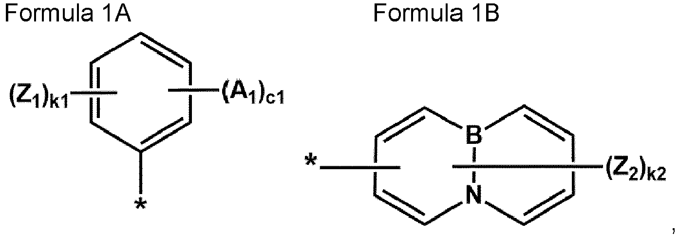 wherein in Formulae 1, 1A, and 1B,M is platinum (Pt), palladium (Pd), copper (Cu), nickel (Ni), silver (Ag), gold (Au), rhodium (Rh), iridium (Ir), ruthenium (Ru), osmium (Os), titanium (Ti), zirconium (Zr), hafnium (Hf), europium (Eu), terbium (Tb), or thulium (Tm),X1 is C, and a bond between X1 and M is a coordinate bond,X2 to X4, Y1, and Y2 are each independently C or N,one of a bond between X2 and M, a bond between X3 and M, and a bond between X4 and M is a coordinate bond, and the other two bonds are each a covalent bond,CY2 to CY4 are each independently a C3-C60 carbocyclic group or a C1-C60 heterocyclic group,L1 to L3 are each independently a single bond, *-O-*', *-S-*', *-Se-*', *-S(=O)2-*', *-C(R5)(R6)-*', *-C(R5)=*', *=C(R5)-*', *-C(R5)=C(R6)-*', *-C(=O)-*', *-C(=S)-*', *-C≡C-*', *-B(R5)-*', *-N(R5)-*', *-P(R5)-*', *-Si(R5)(R6)-*', *-P(=O)(R5)-*', or *-Ge(R5)(R6)-*',a1 to a3 are each independently an integer from 1 to 3,R1 to R6 and R11 are each independently a group represented by Formula 1A, hydrogen, deuterium, -F, -CI, -Br, -I, a hydroxyl group, a cyano group, a nitro group, a C1-C60 alkyl group unsubstituted or substituted with at least one R10a, a C2-C60 alkenyl group unsubstituted or substituted with at least one R10a, a C2-C60 alkynyl group unsubstituted or substituted with at least one R10a, a C1-C60 alkoxy group unsubstituted or substituted with at least one R10a, a C3-C60 carbocyclic group unsubstituted or substituted with at least one R10a, a C1-C60 heterocyclic group unsubstituted or substituted with at least one R10a, a C6-C60 aryloxy group unsubstituted or substituted with at least one R10a, a C6-C60 arylthio group unsubstituted or substituted with at least one R10a, -Si(Q1)(Q2)(Q3), -N(Q1)(Q2), -B(Q1)(Q2), -C(=O)(Q1), -S(=O)2(Q1), or - P(=O)(Q1)(Q2),at least two groups of R1 in a number of b1, R2 in a number of b2, R3 in a number of b3, R4 in a number of b4, R5, and R6 are optionally bound to each other to form a C3-C60 carbocyclic group unsubstituted or substituted with at least one R10a or a C1-C60 heterocyclic group unsubstituted or substituted with at least one R10a,at least one of R11, R1 in a number of b1, R2 in a number of b2, R3 in a number of b3, and R4 in a number of b4 is a group represented by Formula 1A,b1 is 1 or 2,b2 to b4 are each independently an integer from 1 to 10,A1 is a group represented by Formula 1B,c1 is an integer from 1 to 5,Z1 and Z2 are each independently hydrogen, deuterium, -F, -CI, -Br, -I, a hydroxyl group, a cyano group, a nitro group, a C1-C60 alkyl group unsubstituted or substituted with at least one R10a, a C2-C60 alkenyl group unsubstituted or substituted with at least one R10a, a C2-C60 alkynyl group unsubstituted or substituted with at least one R10a, a C1-C60 alkoxy group unsubstituted or substituted with at least one R10a, a C3-C60 carbocyclic group unsubstituted or substituted with at least one R10a, a C1-C60 heterocyclic group unsubstituted or substituted with at least one R10a, a C6-C60 aryloxy group unsubstituted or substituted with at least one R10a, a C6-C60 arylthio group unsubstituted or substituted with at least one R10a, -Si(Q1)(Q2)(Q3), -N(Q1)(Q2), - B(Q1)(Q2), -C(=O)(Q1), -S(=O)2(Q1), or -P(=O)(Q1)(Q2),k1 is an integer from 0 to 4,k2 is an integer from 1 to 7,* and *' each indicate a binding site to an adjacent atom, andR10a is:deuterium, -F, -CI, -Br, -I, a hydroxyl group, a cyano group, or a nitro group;a C1-C60 alkyl group, a C2-C60 alkenyl group, a C2-C60 alkynyl group, or a C1-C60 alkoxy group, each unsubstituted or substituted with deuterium, -F, -CI, -Br, -I, a hydroxyl group, a cyano group, a nitro group, a C3-C60 carbocyclic group, a C1-C60 heterocyclic group, a C6-C60 aryloxy group, a C6-C60 arylthio group, -Si(Q11)(Q12)(Q13), - N(Q11)(Q12), -B(Q11)(Q12), -C(=O)(Q11), -S(=O)2(Q11), -P(=O)(Q11)(Q12), or any combination thereof;a C3-C60 carbocyclic group, a C1-C60 heterocyclic group, a C6-C60 aryloxy group, or a C6-C60 arylthio group, each unsubstituted or substituted with deuterium, -F, -CI, - Br, -I, a hydroxyl group, a cyano group, a nitro group, a C1-C60 alkyl group, a C2-C60 alkenyl group, a C2-C60 alkynyl group, a C1-C60 alkoxy group, a C3-C60 carbocyclic group, a C1-C60 heterocyclic group, a C6-C60 aryloxy group, a C6-C60 arylthio group, - Si(Q21)(Q22)(Q23), -N(Q21)(Q22), -B(Q21)(Q22), -C(=O)(Q21), -S(=O)2(Q21), - P(=O)(Q21)(Q22), or any combination thereof; or-Si(Q31)(Q32)(Q33), -N(Q31)(Q32), -B(Q31)(Q32), -C(=O)(Q31), -S(=O)2(Q31), or - P(=O)(Q31)(Q32), andwherein Q1 to Q3, Q11 to Q13, Q21 to Q23, and Q31 to Q33 are each independently hydrogen; deuterium; -F; -CI; -Br; -I; a hydroxyl group; a cyano group; a nitro group; a C1-C60 alkyl group; a C2-C60 alkenyl group; a C2-C60 alkynyl group; a C1-C60 alkoxy group; or a C3-C60 carbocyclic group or a C1-C60 heterocyclic group, each unsubstituted or substituted with deuterium, -F, a cyano group, a C1-C60 alkyl group, a C1-C60 alkoxy group, a phenyl group, a biphenyl group, or any combination thereof.
 - The light-emitting device of claim 1, wherein the first electrode is an anode,the second electrode is a cathode,the interlayer further comprises a hole transport region between the first electrode and the emission layer, and an electron transport region between the emission layer and the second electrode,the hole transport region comprises a hole injection layer, a hole transport layer, an emission auxiliary layer, an electron blocking layer, or any combination thereof, andthe electron transport region comprises a buffer layer, a hole blocking layer, an electron control layer, an electron transport layer, an electron injection layer, or a combination thereof.
- The light-emitting device of claim 1 or claim 2, wherein
the emission layer comprises the organometallic compound represented by Formula 1. - The light-emitting device of any one of claims 1 to 3, whereinthe emission layer comprises a host and a dopant, andthe dopant comprises the organometallic compound represented by Formula 1.
- The light-emitting device of claim 4, wherein
the host comprises a hole transporting host and an electron transporting host. - The light-emitting device of claim 4, whereinthe host comprises an electron transporting host represented by Formula 2 and a hole transporting host represented by Formula 3:

 wherein, in Formula 2 and Formula 3,X21 is N or C-(L24)a24-(R24)b24, X22 is N or C-(L25)a25-(R25)b25, and X23 is N or C-(L26)a26-(R26)b26,X31 is selected from a single bond, O, S, N(R34), C(R34)(R35), and Si(R34)(R35),CY31 and CY32 are each independently a C3-C60 carbocyclic group or a C1-C60 heterocyclic group,L21 to L26 and L31 to L33 are each independently a C3-C60 carbocyclic group unsubstituted or substituted with at least one R10a or a C1-C60 heterocyclic group unsubstituted or substituted with at least one R10a,a21 to a26 and a31 to a33 are each independently an integer from 0 to 5,R21 to R26 and R31 to R35 are each independently hydrogen, deuterium, -F, -CI, - Br, -I, a hydroxyl group, a cyano group, a nitro group, a C1-C60 alkyl group unsubstituted or substituted with at least one R10a, a C2-C60 alkenyl group unsubstituted or substituted with at least one R10a, a C2-C60 alkynyl group unsubstituted or substituted with at least one R10a, a C1-C60 alkoxy group unsubstituted or substituted with at least one R10a, a C3-C60 carbocyclic group unsubstituted or substituted with at least one R10a, a C1-C60 heterocyclic group unsubstituted or substituted with at least one R10a, a C6-C60 aryloxy group unsubstituted or substituted with at least one R10a, a C6-C60 arylthio group unsubstituted or substituted with at least one R10a, -Si(Q1)(Q2)(Q3), -N(Q1)(Q2), - B(Q1)(Q2), -C(=O)(Q1), -S(=O)2(Q1), or -P(=O)(Q1)(Q2),b21 to b26, b31 to b33, n31, and n32 are each independently an integer from 1 to 5, andR10a is:deuterium, -F, -CI, -Br, -I, a hydroxyl group, a cyano group, or a nitro group;a C1-C60 alkyl group, a C2-C60 alkenyl group, a C2-C60 alkynyl group, or a C1-C60 alkoxy group, each unsubstituted or substituted with deuterium, -F, -CI, -Br, -I, a hydroxyl group, a cyano group, a nitro group, a C3-C60 carbocyclic group, a C1-C60 heterocyclic group, a C6-C60 aryloxy group, a C6-C60 arylthio group, -Si(Q11)(Q12)(Q13), - N(Q11)(Q12), -B(Q11)(Q12), -C(=O)(Q11), -S(=O)2(Q11), -P(=O)(Q11)(Q12), or any combination thereof;a C3-C60 carbocyclic group, a C1-C60 heterocyclic group, a C6-C60 aryloxy group, or a C6-C60 arylthio group, each unsubstituted or substituted with deuterium, -F, -CI, - Br, -I, a hydroxyl group, a cyano group, a nitro group, a C1-C60 alkyl group, a C2-C60 alkenyl group, a C2-C60 alkynyl group, a C1-C60 alkoxy group, a C3-C60 carbocyclic group, a C1-C60 heterocyclic group, a C6-C60 aryloxy group, a C6-C60 arylthio group, - Si(Q21)(Q22)(Q23), -N(Q21)(Q22), -B(Q21)(Q22), -C(=O)(Q21), -S(=O)2(Q21), - P(=O)(Q21)(Q22), or any combination thereof; or-Si(Q31)(Q32)(Q33), -N(Q31)(Q32), -B(Q31)(Q32), -C(=O)(Q31), -S(=O)2(Q31), or - P(=O)(Q31)(Q32), andwherein Q1 to Q3, Q11 to Q13, Q21 to Q23, and Q31 to Q33 are each independently hydrogen; deuterium; -F; -CI; -Br; -I; a hydroxyl group; a cyano group; a nitro group; a C1-C60 alkyl group; a C2-C60 alkenyl group; a C2-C60 alkynyl group; a C1-C60 alkoxy group; or a C3-C60 carbocyclic group or a C1-C60 heterocyclic group, each unsubstituted or substituted with deuterium, -F, a cyano group, a C1-C60 alkyl group, a C1-C60 alkoxy group, a phenyl group, a biphenyl group, or any combination thereof.
 - The light-emitting device of any one of claims 1 to 6, wherein
the light-emitting device further comprises at least one selected from a first capping layer outside the first electrode and a second capping layer outside the second electrode, and the at least one selected from the first capping layer and the second capping layer has a refractive index of about 1.6 or higher at a wavelength of 589 nanometers (nm). - An electronic apparatus comprising the light-emitting device of any one of claims 1 to 7, optionally wherein the electronic apparatus further comprises a color filter, a color-conversion layer, a touchscreen layer, a polarization layer, or any combination thereof.
- An organometallic compound represented by Formula 1:
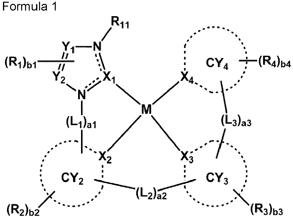
 M is platinum (Pt), palladium (Pd), nickel (Ni), copper (Cu), silver (Ag), gold (Au), rhodium (Rh), iridium (Ir), ruthenium (Ru), osmium (Os), titanium (Ti), zirconium (Zr), hafnium (Hf), europium (Eu), terbium (Tb), or thulium (Tm),X1 is C, and a bond between X1 and M is a coordinate bond,X2 to X4, Y1, and Y2 are each independently C or N,one of a bond between X2 and M, a bond between X3 and M, and a bond between X4 and M is a coordinate bond, and the other two bonds are each a covalent bond,CY2 to CY4 are each independently a C3-C60 carbocyclic group or a C1-C60 heterocyclic group,L1 to L3 are each independently a single bond, *-O-*', *-S-*', *-Se-*', *-S(=O)2-*', *-C(R5)(R6)-*', *-C(R5)=*', *=C(R5)-*', *-C(R5)=C(R6)-*', *-C(=O)-*', *-C(=S)-*', *-C≡C-*', *-B(R5)-*', *-N(R5)-*', *-P(R5)-*', *-Si(R5)(R6)-*', *-P(=O)(R5)-*', or *-Ge(R5)(R6)-*',a1 to a3 are each independently an integer from 1 to 3,R1 to R6 and R11 are each independently a group represented by Formula 1A, hydrogen, deuterium, -F, -CI, -Br, -I, a hydroxyl group, a cyano group, a nitro group, a C1-C60 alkyl group unsubstituted or substituted with at least one R10a, a C2-C60 alkenyl group unsubstituted or substituted with at least one R10a, a C2-C60 alkynyl group unsubstituted or substituted with at least one R10a, a C1-C60 alkoxy group unsubstituted or substituted with at least one R10a, a C3-C60 carbocyclic group unsubstituted or substituted with at least one R10a, a C1-C60 heterocyclic group unsubstituted or substituted with at least one R10a, a C6-C60 aryloxy group unsubstituted or substituted with at least one R10a, a C6-C60 arylthio group unsubstituted or substituted with at least one R10a, -Si(Q1)(Q2)(Q3), -N(Q1)(Q2), -B(Q1)(Q2), -C(=O)(Q1), -S(=O)2(Q1), or - P(=O)(Q1)(Q2),at least two groups of R1 in a number of b1, R2 in a number of b2, R3 in a number of b3, R4 in a number of b4, R5, and R6 are optionally bound to each other to form a C3-C60 carbocyclic group unsubstituted or substituted with at least one R10a or a C1-C60 heterocyclic group unsubstituted or substituted with at least one R10a,at least one of R11, R1 in a number of b1, R2 in a number of b2, R3 in a number of b3, and R4 in a number of b4 is a group represented by Formula 1A,b1 is 1 or 2,b2 to b4 are each independently an integer from 1 to 10,A1 is a group represented by Formula 1B,c1 is an integer from 1 to 5,Z1 and Z2 are each independently hydrogen, deuterium, -F, -CI, -Br, -I, a hydroxyl group, a cyano group, a nitro group, a C1-C60 alkyl group unsubstituted or substituted with at least one R10a, a C2-C60 alkenyl group unsubstituted or substituted with at least one R10a, a C2-C60 alkynyl group unsubstituted or substituted with at least one R10a, a C1-C60 alkoxy group unsubstituted or substituted with at least one R10a, a C3-C60 carbocyclic group unsubstituted or substituted with at least one R10a, a C1-C60 heterocyclic group unsubstituted or substituted with at least one R10a, a C6-C60 aryloxy group unsubstituted or substituted with at least one R10a, a C6-C60 arylthio group unsubstituted or substituted with at least one R10a, -Si(Q1)(Q2)(Q3), -N(Q1)(Q2), - B(Q1)(Q2), -C(=O)(Q1), -S(=O)2(Q1), or -P(=O)(Q1)(Q2),k1 is an integer from 0 to 4,k2 is an integer from 1 to 7,* and *' each indicate a binding site to an adjacent atom, andR10a is:deuterium, -F, -CI, -Br, -I, a hydroxyl group, a cyano group, or a nitro group;a C1-C60 alkyl group, a C2-C60 alkenyl group, a C2-C60 alkynyl group, or a C1-C60 alkoxy group, each unsubstituted or substituted with deuterium, -F, -CI, -Br, -I, a hydroxyl group, a cyano group, a nitro group, a C3-C60 carbocyclic group, a C1-C60 heterocyclic group, a C6-C60 aryloxy group, a C6-C60 arylthio group, -Si(Q11)(Q12)(Q13), - N(Q11)(Q12), -B(Q11)(Q12), -C(=O)(Q11), -S(=O)2(Q11), -P(=O)(Q11)(Q12), or any combination thereof;a C3-C60 carbocyclic group, a C1-C60 heterocyclic group, a C6-C60 aryloxy group, or a C6-C60 arylthio group, each unsubstituted or substituted with deuterium, -F, -CI, - Br, -I, a hydroxyl group, a cyano group, a nitro group, a C1-C60 alkyl group, a C2-C60 alkenyl group, a C2-C60 alkynyl group, a C1-C60 alkoxy group, a C3-C60 carbocyclic group, a C1-C60 heterocyclic group, a C6-C60 aryloxy group, a C6-C60 arylthio group, - Si(Q21)(Q22)(Q23), -N(Q21)(Q22), -B(Q21)(Q22), -C(=O)(Q21), -S(=O)2(Q21), - P(=O)(Q21)(Q22), or any combination thereof; or-Si(Q31)(Q32)(Q33), -N(Q31)(Q32), -B(Q31)(Q32), -C(=O)(Q31), -S(=O)2(Q31), or - P(=O)(Q31)(Q32), andwherein Q1 to Q3, Q11 to Q13, Q21 to Q23, and Q31 to Q33 are each independently hydrogen; deuterium; -F; -CI; -Br; -I; a hydroxyl group; a cyano group; a nitro group; a C1-C60 alkyl group; a C2-C60 alkenyl group; a C2-C60 alkynyl group; a C1-C60 alkoxy group; or a C3-C60 carbocyclic group or a C1-C60 heterocyclic group, each unsubstituted or substituted with deuterium, -F, a cyano group, a C1-C60 alkyl group, a C1-C60 alkoxy group, a phenyl group, a biphenyl group, or any combination thereof.
 - The organometallic compound of claim 9, whereinCY2 is a group represented by one of Formulae CY2-1 to CY2-9,CY3 is a group represented by one of Formulae CY3-1 to CY3-10, and/orCY4 is a group represented by one of Formulae CY4-1 to CY4-9:


 and wherein, in Formulae CY2-1 to CY2-9, CY3-1 to CY3-10, and CY4-1 to CY4-9,Z21 to Z27, Z31 to Z37, and Z41 to Z48 are each independently C or N,Y21, Y31, and Y41 are each independently N, O, S, C, or Si,X2 to X4 are respectively understood by referring to the descriptions of X2 to X4 in Formula 1,* indicates a binding site to M, and*' and *" each indicate a binding site to an adjacent atom.
 - The organometallic compound of claim 9 or claim 10, wherein:(i) L1 is a single bond, L2 is *-O-*' or *-S-*', and L3 is *-N(R5)-*'; and/or(ii) the group represented by Formula 1A is represented by one of Formulae 1A-1 to 1A-14:


 Z11 to Z15 are each independently understood by referring to the description of Z1 in Formula 1A,A11 to A13 are each independently understood by referring to the description of A1 in Formula 1A,A1 is understood by referring to the description of A1 in Formula 1A, and* indicates a binding site to an adjacent atom.
 - The organometallic compound of any one of claims 9 to 11, wherein the group represented by Formula 1A is represented by Formula 1A-7-1:

wherein, in Formula 1A-7-1,Z12 to Z14 are each independently understood by referring to the description of Z1 in Formula 1A,Z21 and Z22 are each independently understood by referring to the description of Z2 in Formula 1B,k21 and k22 are each independently an integer from 1 to 7, and* indicates a binding site to an adjacent atom. - The organometallic compound of any one of claims 9 to 12, wherein:(i) at least one of R1 in a number of b1, R2 in a number of b2, R3 in a number of b3, R4 in a number of b4, R5, R6, and R11 is deuterium, -CH2D, -CHD2, -CD3, a phenyl group substituted with at least one deuterium, or a group represented by one of Formulae 10-2 to 10-7:
 "D" represents deuterium, and* indicates a binding site to an adjacent atom; and/or(ii) a moiety represented by
 R1a to R1d are each independently understood by referring to the description of R1 in Formula 1,R2a to R2c are each independently understood by referring to the description of R2 in Formula 1,M, A1, c1, Z1, and k1 are respectively understood by referring to the descriptions of M, A1, c1, Z1, and k1 in Formulae 1 and 1A, and* indicates a binding site to L2; and/or(iii) a moiety represented by

wherein, in Formulae L2-1 and L2-2,R3a and R3b are each independently understood by referring to the description of R3 in Formula 1,R4a to R4e are each independently understood by referring to the description of R4 in Formula 1,R5a to R5d are each independently understood by referring to the description of R10a in Formula 1,M is understood by referring to the description of M in Formula 1, and* indicates a binding site to L2. - The organometallic compound of any one of claims 9 to 13, wherein the organometallic compound is represented by any one selected from Formulae 1-1 to 1-4:

 M, L2, A1, c1, Z1, and k1 are respectively understood by referring to the descriptions of M, L2, A1, c1, Z1, and k1 in Formulae 1 and 1A,R1a to R1d, R2a to R2c, R3a, R3b, R4a to R4e, and R5a to R5d are each independently hydrogen, deuterium, -F, -CI, -Br, -I, -CH2D, -CHD2, -CD3, -CH2F, -CHF2, -CF3, a hydroxyl group, a cyano group, a nitro group, a methyl group, an ethyl group, a propyl group, an iso-propyl group, an n-butyl group, an iso-butyl group, a sec-butyl group, a tert-butyl group, an n-pentyl group, a tert-pentyl group, a neo-pentyl group, an isopentyl group, a sec-pentyl group, a 3-pentyl group, a sec-isopentyl group, an n-hexyl group, an iso-hexyl group, a sec-hexyl group, a tert-hexyl group, or a group represented by one selected from the group consisting of Formulae 9-1 to 9-31 and 10-1 to 10-7:


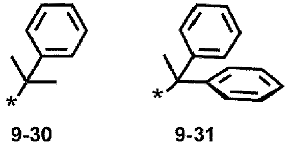

wherein, in Formulae 9-1 to 9-31 and 10-1 to 10-7,"Et" represents an ethyl group,"i-Pr" represents an iso-propyl group,"t-Bu" represents a tert-butyl group,"D" represents deuterium, and* indicates a binding site to an adjacent atom, optionally wherein, in Formulae 1-1 to 1-4, at least one of R1a to R1d, R2a to R2c, R3a, R3b, R4a to R4e, and R5a to R5d is deuterium, -CH2D, -CHD2, -CD3, or a group represented by one of Formulae 10-1 to 10-7: wherein, in Formulae 10-1 to 10-7,"D" represents deuterium, and* indicates a binding site to an adjacent atom.
 - The organometallic compound of claim 9, wherein the organometallic compound is represented by one of Compounds BD01 to BD210:





Applications Claiming Priority (1)
| Application Number | Priority Date | Filing Date | Title |
|---|---|---|---|
| KR1020200166929A KR102779968B1 (en) | 2020-12-02 | 2020-12-02 | Organometallic compound and light emitting device including the same and electronic apparatus including the same |
Publications (3)
| Publication Number | Publication Date |
|---|---|
| EP4008758A2 true EP4008758A2 (en) | 2022-06-08 |
| EP4008758A3 EP4008758A3 (en) | 2022-07-06 |
| EP4008758B1 EP4008758B1 (en) | 2023-09-06 |
Family
ID=78528817
Family Applications (1)
| Application Number | Title | Priority Date | Filing Date |
|---|---|---|---|
| EP21206644.3A Active EP4008758B1 (en) | 2020-12-02 | 2021-11-05 | Organometallic compound, light-emitting device including organometallic compound, and electronic apparatus including light-emitting device |
Country Status (4)
| Country | Link |
|---|---|
| US (1) | US12302744B2 (en) |
| EP (1) | EP4008758B1 (en) |
| KR (1) | KR102779968B1 (en) |
| CN (1) | CN114583071A (en) |
Families Citing this family (3)
| Publication number | Priority date | Publication date | Assignee | Title |
|---|---|---|---|---|
| KR20230111664A (en) * | 2022-01-17 | 2023-07-26 | 삼성디스플레이 주식회사 | Light emitting device and organometallic compound for the light emitting device |
| KR20240055181A (en) * | 2022-10-18 | 2024-04-29 | 삼성디스플레이 주식회사 | Organic photodiode and electronic device comprising organic photodiode and organic light emitting device |
| KR20240113629A (en) * | 2023-01-12 | 2024-07-23 | 삼성디스플레이 주식회사 | Light emitting device including organometallic compound, electronic apparatus including the light emitting device and the organometallic compound |
Family Cites Families (32)
| Publication number | Priority date | Publication date | Assignee | Title |
|---|---|---|---|---|
| US6939624B2 (en) | 2000-08-11 | 2005-09-06 | Universal Display Corporation | Organometallic compounds and emission-shifting organic electrophosphorescence |
| KR100537621B1 (en) | 2004-02-02 | 2005-12-19 | 삼성에스디아이 주식회사 | Iridium compound and organic electroluminescent display device using the same |
| US7393599B2 (en) | 2004-05-18 | 2008-07-01 | The University Of Southern California | Luminescent compounds with carbene ligands |
| KR100730115B1 (en) | 2004-06-23 | 2007-06-19 | 삼성에스디아이 주식회사 | Iridium compound and organic electroluminescent device using same |
| DE102004057072A1 (en) | 2004-11-25 | 2006-06-01 | Basf Ag | Use of Transition Metal Carbene Complexes in Organic Light Emitting Diodes (OLEDs) |
| KR101223717B1 (en) | 2005-04-12 | 2013-01-18 | 삼성디스플레이 주식회사 | Silyl substituted cyclometalated transition metal complex and organic electroluminescence device using the same |
| US9051344B2 (en) | 2005-05-06 | 2015-06-09 | Universal Display Corporation | Stability OLED materials and devices |
| JP2007045742A (en) | 2005-08-10 | 2007-02-22 | Mitsubishi Chemicals Corp | Process for producing transition metal complex and transition metal complex |
| US8106199B2 (en) | 2007-02-13 | 2012-01-31 | Arizona Board Of Regents For And On Behalf Of Arizona State University | Organometallic materials for optical emission, optical absorption, and devices including organometallic materials |
| WO2009086209A2 (en) | 2007-12-21 | 2009-07-09 | Arizona Board Of Regents For And On Behalf Of Arizona State University | Platinum(ii) di(2-pyrazolyl)benzene chloride analogs and uses |
| US8389725B2 (en) | 2008-02-29 | 2013-03-05 | Arizona Board Of Regents For And On Behalf Of Arizona State University | Tridentate platinum (II) complexes |
| WO2010118026A2 (en) | 2009-04-06 | 2010-10-14 | Arizona Board Of Regents Acting For And On Behalf Of Arizona State University | Synthesis of four coordinated platinum complexes and their applications in light emitting devices thereof |
| TWI419955B (en) | 2009-04-23 | 2013-12-21 | Chien Hong Cheng | Β-diketone ancillary ligands and their metal complexes used in organic optolelectronic devices |
| US8586203B2 (en) | 2009-05-20 | 2013-11-19 | Universal Display Corporation | Metal complexes with boron-nitrogen heterocycle containing ligands |
| JP2013530135A (en) | 2010-04-30 | 2013-07-25 | アリゾナ ボード オブ リージェンツ アクティング フォー アンド オン ビハーフ オブ アリゾナ ステイト ユニバーシティ | Synthesis of tetracoordinate palladium complex and its application in light-emitting devices |
| JP2013525436A (en) | 2010-04-30 | 2013-06-20 | アリゾナ ボード オブ リージェンツ アクティング フォー アンド オン ビハーフ オブ アリゾナ ステイト ユニバーシティ | Synthesis of tetracoordinated gold complex and its application in light-emitting devices |
| TWI541247B (en) | 2011-02-18 | 2016-07-11 | 美國亞利桑那州立大學董事會 | Four-coordinate platinum and palladium complex with geometrically distortion charge transfer state and its application in illuminating devices |
| US8883322B2 (en) | 2011-03-08 | 2014-11-11 | Universal Display Corporation | Pyridyl carbene phosphorescent emitters |
| US9221857B2 (en) | 2011-04-14 | 2015-12-29 | Arizona Board Of Regents Acting For And On Behalf Of Arizona State University | Pyridine-oxyphenyl coordinated iridium (III) complexes and methods of making and using |
| WO2012162488A1 (en) | 2011-05-26 | 2012-11-29 | Arizona Board Of Regents Acting For And On Behalf Of Arizona State University | Synthesis of platinum and palladium complexes as narrow-band phosphorescent emitters for full color displays |
| US9231218B2 (en) * | 2012-07-10 | 2016-01-05 | Universal Display Corporation | Phosphorescent emitters containing dibenzo[1,4]azaborinine structure |
| US9312502B2 (en) | 2012-08-10 | 2016-04-12 | Arizona Board Of Regents Acting For And On Behalf Of Arizona State University | Iridium complexes demonstrating broadband emission through controlled geometric distortion and applications thereof |
| US9312505B2 (en) * | 2012-09-25 | 2016-04-12 | Universal Display Corporation | Organic electroluminescent materials and devices |
| CN104232076B (en) | 2013-06-10 | 2019-01-15 | 代表亚利桑那大学的亚利桑那校董会 | Phosphorescent tetradentate metal complexes with improved emission spectra |
| US9224963B2 (en) | 2013-12-09 | 2015-12-29 | Arizona Board Of Regents On Behalf Of Arizona State University | Stable emitters |
| US9871212B2 (en) * | 2014-11-14 | 2018-01-16 | Universal Display Corporation | Organic electroluminescent materials and devices |
| CN104370974B (en) | 2014-12-04 | 2018-01-23 | 南京大学 | One kind is using nitrogen heterocyclic ring Cabbeen as complex of iridium of the second main part and preparation method thereof |
| US11725022B2 (en) | 2017-06-23 | 2023-08-15 | Universal Display Corporation | Organic electroluminescent materials and devices |
| US11552261B2 (en) * | 2017-06-23 | 2023-01-10 | Universal Display Corporation | Organic electroluminescent materials and devices |
| US11802136B2 (en) | 2017-06-23 | 2023-10-31 | Universal Display Corporation | Organic electroluminescent materials and devices |
| EP3508491B1 (en) * | 2018-01-05 | 2020-09-09 | Samsung Electronics Co., Ltd. | Organometallic compound, organic light-emitting device including the same, and diagnostic composition including the same |
| US11476430B2 (en) | 2018-10-15 | 2022-10-18 | Universal Display Corporation | Organic electroluminescent materials and devices |
-
2020
- 2020-12-02 KR KR1020200166929A patent/KR102779968B1/en active Active
-
2021
- 2021-07-28 US US17/443,933 patent/US12302744B2/en active Active
- 2021-11-05 EP EP21206644.3A patent/EP4008758B1/en active Active
- 2021-11-08 CN CN202111312607.XA patent/CN114583071A/en active Pending
Also Published As
| Publication number | Publication date |
|---|---|
| KR20220078010A (en) | 2022-06-10 |
| US20220173338A1 (en) | 2022-06-02 |
| US12302744B2 (en) | 2025-05-13 |
| EP4008758B1 (en) | 2023-09-06 |
| EP4008758A3 (en) | 2022-07-06 |
| CN114583071A (en) | 2022-06-03 |
| KR102779968B1 (en) | 2025-03-13 |
Similar Documents
| Publication | Publication Date | Title |
|---|---|---|
| US20220020939A1 (en) | Light-emitting device and electronic apparatus including the light-emitting device | |
| KR102883832B1 (en) | Organometallic compound, light emitting device including the same and electronic apparatus including the light emitting device | |
| EP4008758B1 (en) | Organometallic compound, light-emitting device including organometallic compound, and electronic apparatus including light-emitting device | |
| US20250081839A1 (en) | Heterocyclic compound, light-emitting device including heterocyclic compound, and electronic apparatus including light-emitting device | |
| US20220336760A1 (en) | Organometallic compound, light-emitting device including organometallic compound, and electronic apparatus including light-emitting device | |
| KR102870801B1 (en) | Organometallic compound and light emitting device including the same and electronic apparatus including the same | |
| EP4142454B1 (en) | Heterocyclic compound and light-emitting device including the heterocyclic compound | |
| CN114262350A (en) | Organometallic compound, light-emitting device including organometallic compound, and electronic apparatus including light-emitting device | |
| CN113801168A (en) | Organometallic compound, light-emitting device including organometallic compound, and electronic device including light-emitting device | |
| EP4219497A1 (en) | Heterocyclic compound, light-emitting device including the heterocyclic compound and electronic apparatus including the light-emitting device | |
| US20230041701A1 (en) | Organometallic compound, light-emitting device including the same, and electronic apparatus including the light-emitting device | |
| KR102897061B1 (en) | A heterocyclic compound and light emitting device comprising the same | |
| KR102867203B1 (en) | Light emitting device, electronic apparatus including the same and organometallic compound | |
| KR102866750B1 (en) | condensed cyclic compound and light emitting device including the same | |
| KR20220141933A (en) | Condensed cylic compound, light emitting device including the condensed cyclic compound and electronic apparatus including the light emitting device | |
| EP4203647B1 (en) | Light-emitting device and electronic apparatus including the same | |
| KR102942301B1 (en) | Heterocyclic compound and light emitting device including the same | |
| US20230240142A1 (en) | Condensed cyclic compound, light-emitting device including the same, and electronic apparatus including the light-emitting device | |
| KR102840570B1 (en) | Light emitting device comprising condensed cyclic compound and electronic apparatus comprising the device | |
| KR102914862B1 (en) | Light emitting device including organometallic compound, electronic apparatus including the light emitting device and the organometallic compound | |
| US20230225189A1 (en) | Light-emitting device including organometallic compound, electronic apparatus including the light-emitting device, and the organometallic compound | |
| US20230140120A1 (en) | Light-emitting device including heterocyclic compound and electronic apparatus including the light-emitting device | |
| US20230116536A1 (en) | Light-emitting device including amine compound, electronic apparatus including light-emitting device, and amine compound | |
| EP4112601A1 (en) | Condensed cyclic compound, light-emitting device including the same, and electronic apparatus including the light-emitting device | |
| US20220293864A1 (en) | Light-emitting device |
Legal Events
| Date | Code | Title | Description |
|---|---|---|---|
| PUAI | Public reference made under article 153(3) epc to a published international application that has entered the european phase |
Free format text: ORIGINAL CODE: 0009012 |
|
| STAA | Information on the status of an ep patent application or granted ep patent |
Free format text: STATUS: THE APPLICATION HAS BEEN PUBLISHED |
|
| PUAL | Search report despatched |
Free format text: ORIGINAL CODE: 0009013 |
|
| AK | Designated contracting states |
Kind code of ref document: A2 Designated state(s): AL AT BE BG CH CY CZ DE DK EE ES FI FR GB GR HR HU IE IS IT LI LT LU LV MC MK MT NL NO PL PT RO RS SE SI SK SM TR |
|
| AK | Designated contracting states |
Kind code of ref document: A3 Designated state(s): AL AT BE BG CH CY CZ DE DK EE ES FI FR GB GR HR HU IE IS IT LI LT LU LV MC MK MT NL NO PL PT RO RS SE SI SK SM TR |
|
| RIC1 | Information provided on ipc code assigned before grant |
Ipc: H01L 51/00 20060101ALI20220530BHEP Ipc: C07F 15/00 20060101ALI20220530BHEP Ipc: C09K 11/06 20060101AFI20220530BHEP |
|
| STAA | Information on the status of an ep patent application or granted ep patent |
Free format text: STATUS: REQUEST FOR EXAMINATION WAS MADE |
|
| 17P | Request for examination filed |
Effective date: 20221114 |
|
| RBV | Designated contracting states (corrected) |
Designated state(s): AL AT BE BG CH CY CZ DE DK EE ES FI FR GB GR HR HU IE IS IT LI LT LU LV MC MK MT NL NO PL PT RO RS SE SI SK SM TR |
|
| GRAP | Despatch of communication of intention to grant a patent |
Free format text: ORIGINAL CODE: EPIDOSNIGR1 |
|
| STAA | Information on the status of an ep patent application or granted ep patent |
Free format text: STATUS: GRANT OF PATENT IS INTENDED |
|
| RIC1 | Information provided on ipc code assigned before grant |
Ipc: C07F 5/02 20060101ALI20230310BHEP Ipc: C07B 59/00 20060101ALI20230310BHEP Ipc: C07F 15/00 20060101ALI20230310BHEP Ipc: C09K 11/06 20060101AFI20230310BHEP |
|
| INTG | Intention to grant announced |
Effective date: 20230331 |
|
| P01 | Opt-out of the competence of the unified patent court (upc) registered |
Effective date: 20230516 |
|
| GRAS | Grant fee paid |
Free format text: ORIGINAL CODE: EPIDOSNIGR3 |
|
| GRAA | (expected) grant |
Free format text: ORIGINAL CODE: 0009210 |
|
| STAA | Information on the status of an ep patent application or granted ep patent |
Free format text: STATUS: THE PATENT HAS BEEN GRANTED |
|
| AK | Designated contracting states |
Kind code of ref document: B1 Designated state(s): AL AT BE BG CH CY CZ DE DK EE ES FI FR GB GR HR HU IE IS IT LI LT LU LV MC MK MT NL NO PL PT RO RS SE SI SK SM TR |
|
| REG | Reference to a national code |
Ref country code: GB Ref legal event code: FG4D |
|
| REG | Reference to a national code |
Ref country code: CH Ref legal event code: EP |
|
| REG | Reference to a national code |
Ref country code: DE Ref legal event code: R096 Ref document number: 602021004930 Country of ref document: DE |
|
| REG | Reference to a national code |
Ref country code: IE Ref legal event code: FG4D |
|
| REG | Reference to a national code |
Ref country code: LT Ref legal event code: MG9D |
|
| REG | Reference to a national code |
Ref country code: NL Ref legal event code: MP Effective date: 20230906 |
|
| PG25 | Lapsed in a contracting state [announced via postgrant information from national office to epo] |
Ref country code: GR Free format text: LAPSE BECAUSE OF FAILURE TO SUBMIT A TRANSLATION OF THE DESCRIPTION OR TO PAY THE FEE WITHIN THE PRESCRIBED TIME-LIMIT Effective date: 20231207 |
|
| PG25 | Lapsed in a contracting state [announced via postgrant information from national office to epo] |
Ref country code: SE Free format text: LAPSE BECAUSE OF FAILURE TO SUBMIT A TRANSLATION OF THE DESCRIPTION OR TO PAY THE FEE WITHIN THE PRESCRIBED TIME-LIMIT Effective date: 20230906 Ref country code: RS Free format text: LAPSE BECAUSE OF FAILURE TO SUBMIT A TRANSLATION OF THE DESCRIPTION OR TO PAY THE FEE WITHIN THE PRESCRIBED TIME-LIMIT Effective date: 20230906 Ref country code: NO Free format text: LAPSE BECAUSE OF FAILURE TO SUBMIT A TRANSLATION OF THE DESCRIPTION OR TO PAY THE FEE WITHIN THE PRESCRIBED TIME-LIMIT Effective date: 20231206 Ref country code: LV Free format text: LAPSE BECAUSE OF FAILURE TO SUBMIT A TRANSLATION OF THE DESCRIPTION OR TO PAY THE FEE WITHIN THE PRESCRIBED TIME-LIMIT Effective date: 20230906 Ref country code: LT Free format text: LAPSE BECAUSE OF FAILURE TO SUBMIT A TRANSLATION OF THE DESCRIPTION OR TO PAY THE FEE WITHIN THE PRESCRIBED TIME-LIMIT Effective date: 20230906 Ref country code: HR Free format text: LAPSE BECAUSE OF FAILURE TO SUBMIT A TRANSLATION OF THE DESCRIPTION OR TO PAY THE FEE WITHIN THE PRESCRIBED TIME-LIMIT Effective date: 20230906 Ref country code: GR Free format text: LAPSE BECAUSE OF FAILURE TO SUBMIT A TRANSLATION OF THE DESCRIPTION OR TO PAY THE FEE WITHIN THE PRESCRIBED TIME-LIMIT Effective date: 20231207 Ref country code: FI Free format text: LAPSE BECAUSE OF FAILURE TO SUBMIT A TRANSLATION OF THE DESCRIPTION OR TO PAY THE FEE WITHIN THE PRESCRIBED TIME-LIMIT Effective date: 20230906 |
|
| REG | Reference to a national code |
Ref country code: AT Ref legal event code: MK05 Ref document number: 1608575 Country of ref document: AT Kind code of ref document: T Effective date: 20230906 |
|
| PG25 | Lapsed in a contracting state [announced via postgrant information from national office to epo] |
Ref country code: NL Free format text: LAPSE BECAUSE OF FAILURE TO SUBMIT A TRANSLATION OF THE DESCRIPTION OR TO PAY THE FEE WITHIN THE PRESCRIBED TIME-LIMIT Effective date: 20230906 |
|
| PG25 | Lapsed in a contracting state [announced via postgrant information from national office to epo] |
Ref country code: IS Free format text: LAPSE BECAUSE OF FAILURE TO SUBMIT A TRANSLATION OF THE DESCRIPTION OR TO PAY THE FEE WITHIN THE PRESCRIBED TIME-LIMIT Effective date: 20240106 |
|
| PG25 | Lapsed in a contracting state [announced via postgrant information from national office to epo] |
Ref country code: AT Free format text: LAPSE BECAUSE OF FAILURE TO SUBMIT A TRANSLATION OF THE DESCRIPTION OR TO PAY THE FEE WITHIN THE PRESCRIBED TIME-LIMIT Effective date: 20230906 |
|
| PG25 | Lapsed in a contracting state [announced via postgrant information from national office to epo] |
Ref country code: ES Free format text: LAPSE BECAUSE OF FAILURE TO SUBMIT A TRANSLATION OF THE DESCRIPTION OR TO PAY THE FEE WITHIN THE PRESCRIBED TIME-LIMIT Effective date: 20230906 |
|
| PG25 | Lapsed in a contracting state [announced via postgrant information from national office to epo] |
Ref country code: SM Free format text: LAPSE BECAUSE OF FAILURE TO SUBMIT A TRANSLATION OF THE DESCRIPTION OR TO PAY THE FEE WITHIN THE PRESCRIBED TIME-LIMIT Effective date: 20230906 Ref country code: RO Free format text: LAPSE BECAUSE OF FAILURE TO SUBMIT A TRANSLATION OF THE DESCRIPTION OR TO PAY THE FEE WITHIN THE PRESCRIBED TIME-LIMIT Effective date: 20230906 Ref country code: IS Free format text: LAPSE BECAUSE OF FAILURE TO SUBMIT A TRANSLATION OF THE DESCRIPTION OR TO PAY THE FEE WITHIN THE PRESCRIBED TIME-LIMIT Effective date: 20240106 Ref country code: ES Free format text: LAPSE BECAUSE OF FAILURE TO SUBMIT A TRANSLATION OF THE DESCRIPTION OR TO PAY THE FEE WITHIN THE PRESCRIBED TIME-LIMIT Effective date: 20230906 Ref country code: EE Free format text: LAPSE BECAUSE OF FAILURE TO SUBMIT A TRANSLATION OF THE DESCRIPTION OR TO PAY THE FEE WITHIN THE PRESCRIBED TIME-LIMIT Effective date: 20230906 Ref country code: CZ Free format text: LAPSE BECAUSE OF FAILURE TO SUBMIT A TRANSLATION OF THE DESCRIPTION OR TO PAY THE FEE WITHIN THE PRESCRIBED TIME-LIMIT Effective date: 20230906 Ref country code: AT Free format text: LAPSE BECAUSE OF FAILURE TO SUBMIT A TRANSLATION OF THE DESCRIPTION OR TO PAY THE FEE WITHIN THE PRESCRIBED TIME-LIMIT Effective date: 20230906 Ref country code: PT Free format text: LAPSE BECAUSE OF FAILURE TO SUBMIT A TRANSLATION OF THE DESCRIPTION OR TO PAY THE FEE WITHIN THE PRESCRIBED TIME-LIMIT Effective date: 20240108 Ref country code: SK Free format text: LAPSE BECAUSE OF FAILURE TO SUBMIT A TRANSLATION OF THE DESCRIPTION OR TO PAY THE FEE WITHIN THE PRESCRIBED TIME-LIMIT Effective date: 20230906 |
|
| PG25 | Lapsed in a contracting state [announced via postgrant information from national office to epo] |
Ref country code: PL Free format text: LAPSE BECAUSE OF FAILURE TO SUBMIT A TRANSLATION OF THE DESCRIPTION OR TO PAY THE FEE WITHIN THE PRESCRIBED TIME-LIMIT Effective date: 20230906 Ref country code: IT Free format text: LAPSE BECAUSE OF FAILURE TO SUBMIT A TRANSLATION OF THE DESCRIPTION OR TO PAY THE FEE WITHIN THE PRESCRIBED TIME-LIMIT Effective date: 20230906 |
|
| REG | Reference to a national code |
Ref country code: DE Ref legal event code: R097 Ref document number: 602021004930 Country of ref document: DE |
|
| PG25 | Lapsed in a contracting state [announced via postgrant information from national office to epo] |
Ref country code: MC Free format text: LAPSE BECAUSE OF FAILURE TO SUBMIT A TRANSLATION OF THE DESCRIPTION OR TO PAY THE FEE WITHIN THE PRESCRIBED TIME-LIMIT Effective date: 20230906 |
|
| PG25 | Lapsed in a contracting state [announced via postgrant information from national office to epo] |
Ref country code: DK Free format text: LAPSE BECAUSE OF FAILURE TO SUBMIT A TRANSLATION OF THE DESCRIPTION OR TO PAY THE FEE WITHIN THE PRESCRIBED TIME-LIMIT Effective date: 20230906 |
|
| PLBE | No opposition filed within time limit |
Free format text: ORIGINAL CODE: 0009261 |
|
| STAA | Information on the status of an ep patent application or granted ep patent |
Free format text: STATUS: NO OPPOSITION FILED WITHIN TIME LIMIT |
|
| PG25 | Lapsed in a contracting state [announced via postgrant information from national office to epo] |
Ref country code: LU Free format text: LAPSE BECAUSE OF NON-PAYMENT OF DUE FEES Effective date: 20231105 |
|
| PG25 | Lapsed in a contracting state [announced via postgrant information from national office to epo] |
Ref country code: MC Free format text: LAPSE BECAUSE OF FAILURE TO SUBMIT A TRANSLATION OF THE DESCRIPTION OR TO PAY THE FEE WITHIN THE PRESCRIBED TIME-LIMIT Effective date: 20230906 Ref country code: LU Free format text: LAPSE BECAUSE OF NON-PAYMENT OF DUE FEES Effective date: 20231105 Ref country code: DK Free format text: LAPSE BECAUSE OF FAILURE TO SUBMIT A TRANSLATION OF THE DESCRIPTION OR TO PAY THE FEE WITHIN THE PRESCRIBED TIME-LIMIT Effective date: 20230906 Ref country code: SI Free format text: LAPSE BECAUSE OF FAILURE TO SUBMIT A TRANSLATION OF THE DESCRIPTION OR TO PAY THE FEE WITHIN THE PRESCRIBED TIME-LIMIT Effective date: 20230906 |
|
| REG | Reference to a national code |
Ref country code: BE Ref legal event code: MM Effective date: 20231130 |
|
| 26N | No opposition filed |
Effective date: 20240607 |
|
| REG | Reference to a national code |
Ref country code: IE Ref legal event code: MM4A |
|
| PG25 | Lapsed in a contracting state [announced via postgrant information from national office to epo] |
Ref country code: IE Free format text: LAPSE BECAUSE OF NON-PAYMENT OF DUE FEES Effective date: 20231105 |
|
| PG25 | Lapsed in a contracting state [announced via postgrant information from national office to epo] |
Ref country code: BE Free format text: LAPSE BECAUSE OF NON-PAYMENT OF DUE FEES Effective date: 20231130 |
|
| PG25 | Lapsed in a contracting state [announced via postgrant information from national office to epo] |
Ref country code: IE Free format text: LAPSE BECAUSE OF NON-PAYMENT OF DUE FEES Effective date: 20231105 Ref country code: BE Free format text: LAPSE BECAUSE OF NON-PAYMENT OF DUE FEES Effective date: 20231130 |
|
| PG25 | Lapsed in a contracting state [announced via postgrant information from national office to epo] |
Ref country code: BG Free format text: LAPSE BECAUSE OF FAILURE TO SUBMIT A TRANSLATION OF THE DESCRIPTION OR TO PAY THE FEE WITHIN THE PRESCRIBED TIME-LIMIT Effective date: 20230906 |
|
| PG25 | Lapsed in a contracting state [announced via postgrant information from national office to epo] |
Ref country code: BG Free format text: LAPSE BECAUSE OF FAILURE TO SUBMIT A TRANSLATION OF THE DESCRIPTION OR TO PAY THE FEE WITHIN THE PRESCRIBED TIME-LIMIT Effective date: 20230906 |
|
| REG | Reference to a national code |
Ref country code: CH Ref legal event code: PL |
|
| REG | Reference to a national code |
Ref country code: CH Ref legal event code: PL |
|
| PG25 | Lapsed in a contracting state [announced via postgrant information from national office to epo] |
Ref country code: CH Free format text: LAPSE BECAUSE OF NON-PAYMENT OF DUE FEES Effective date: 20241130 |
|
| PG25 | Lapsed in a contracting state [announced via postgrant information from national office to epo] |
Ref country code: CY Free format text: LAPSE BECAUSE OF FAILURE TO SUBMIT A TRANSLATION OF THE DESCRIPTION OR TO PAY THE FEE WITHIN THE PRESCRIBED TIME-LIMIT; INVALID AB INITIO Effective date: 20211105 |
|
| PG25 | Lapsed in a contracting state [announced via postgrant information from national office to epo] |
Ref country code: TR Free format text: LAPSE BECAUSE OF FAILURE TO SUBMIT A TRANSLATION OF THE DESCRIPTION OR TO PAY THE FEE WITHIN THE PRESCRIBED TIME-LIMIT Effective date: 20230906 |
|
| PGFP | Annual fee paid to national office [announced via postgrant information from national office to epo] |
Ref country code: DE Payment date: 20251020 Year of fee payment: 5 |
|
| PGFP | Annual fee paid to national office [announced via postgrant information from national office to epo] |
Ref country code: GB Payment date: 20251023 Year of fee payment: 5 |
|
| PGFP | Annual fee paid to national office [announced via postgrant information from national office to epo] |
Ref country code: FR Payment date: 20251021 Year of fee payment: 5 |
|
| PG25 | Lapsed in a contracting state [announced via postgrant information from national office to epo] |
Ref country code: HU Free format text: LAPSE BECAUSE OF FAILURE TO SUBMIT A TRANSLATION OF THE DESCRIPTION OR TO PAY THE FEE WITHIN THE PRESCRIBED TIME-LIMIT; INVALID AB INITIO Effective date: 20211105 |