EP4008045B1 - Method for reducing magnetic field emission for heated seats and other applications - Google Patents
Method for reducing magnetic field emission for heated seats and other applications Download PDFInfo
- Publication number
- EP4008045B1 EP4008045B1 EP20754374.5A EP20754374A EP4008045B1 EP 4008045 B1 EP4008045 B1 EP 4008045B1 EP 20754374 A EP20754374 A EP 20754374A EP 4008045 B1 EP4008045 B1 EP 4008045B1
- Authority
- EP
- European Patent Office
- Prior art keywords
- power mosfet
- gate voltage
- current
- duty cycle
- frequency
- Prior art date
- Legal status (The legal status is an assumption and is not a legal conclusion. Google has not performed a legal analysis and makes no representation as to the accuracy of the status listed.)
- Active
Links
Images



Classifications
-
- H—ELECTRICITY
- H05—ELECTRIC TECHNIQUES NOT OTHERWISE PROVIDED FOR
- H05B—ELECTRIC HEATING; ELECTRIC LIGHT SOURCES NOT OTHERWISE PROVIDED FOR; CIRCUIT ARRANGEMENTS FOR ELECTRIC LIGHT SOURCES, IN GENERAL
- H05B1/00—Details of electric heating devices
- H05B1/02—Automatic switching arrangements specially adapted to apparatus ; Control of heating devices
- H05B1/0202—Switches
- H05B1/0219—Switches actuated by modification of the magnetic properties of a material
-
- H—ELECTRICITY
- H02—GENERATION; CONVERSION OR DISTRIBUTION OF ELECTRIC POWER
- H02M—APPARATUS FOR CONVERSION BETWEEN AC AND AC, BETWEEN AC AND DC, OR BETWEEN DC AND DC, AND FOR USE WITH MAINS OR SIMILAR POWER SUPPLY SYSTEMS; CONVERSION OF DC OR AC INPUT POWER INTO SURGE OUTPUT POWER; CONTROL OR REGULATION THEREOF
- H02M1/00—Details of apparatus for conversion
- H02M1/08—Circuits specially adapted for the generation of control voltages for semiconductor devices incorporated in static converters
-
- B—PERFORMING OPERATIONS; TRANSPORTING
- B60—VEHICLES IN GENERAL
- B60N—SEATS SPECIALLY ADAPTED FOR VEHICLES; VEHICLE PASSENGER ACCOMMODATION NOT OTHERWISE PROVIDED FOR
- B60N2/00—Seats specially adapted for vehicles; Arrangement or mounting of seats in vehicles
- B60N2/56—Heating or ventilating devices
- B60N2/5678—Heating or ventilating devices characterised by electrical systems
- B60N2/5685—Resistance
-
- H—ELECTRICITY
- H02—GENERATION; CONVERSION OR DISTRIBUTION OF ELECTRIC POWER
- H02H—EMERGENCY PROTECTIVE CIRCUIT ARRANGEMENTS
- H02H9/00—Emergency protective circuit arrangements for limiting excess current or voltage without disconnection
- H02H9/02—Emergency protective circuit arrangements for limiting excess current or voltage without disconnection responsive to excess current
-
- H—ELECTRICITY
- H02—GENERATION; CONVERSION OR DISTRIBUTION OF ELECTRIC POWER
- H02H—EMERGENCY PROTECTIVE CIRCUIT ARRANGEMENTS
- H02H9/00—Emergency protective circuit arrangements for limiting excess current or voltage without disconnection
- H02H9/02—Emergency protective circuit arrangements for limiting excess current or voltage without disconnection responsive to excess current
- H02H9/025—Current limitation using field effect transistors
-
- H—ELECTRICITY
- H02—GENERATION; CONVERSION OR DISTRIBUTION OF ELECTRIC POWER
- H02M—APPARATUS FOR CONVERSION BETWEEN AC AND AC, BETWEEN AC AND DC, OR BETWEEN DC AND DC, AND FOR USE WITH MAINS OR SIMILAR POWER SUPPLY SYSTEMS; CONVERSION OF DC OR AC INPUT POWER INTO SURGE OUTPUT POWER; CONTROL OR REGULATION THEREOF
- H02M1/00—Details of apparatus for conversion
- H02M1/32—Means for protecting converters other than automatic disconnection
-
- H—ELECTRICITY
- H02—GENERATION; CONVERSION OR DISTRIBUTION OF ELECTRIC POWER
- H02M—APPARATUS FOR CONVERSION BETWEEN AC AND AC, BETWEEN AC AND DC, OR BETWEEN DC AND DC, AND FOR USE WITH MAINS OR SIMILAR POWER SUPPLY SYSTEMS; CONVERSION OF DC OR AC INPUT POWER INTO SURGE OUTPUT POWER; CONTROL OR REGULATION THEREOF
- H02M1/00—Details of apparatus for conversion
- H02M1/44—Circuits or arrangements for compensating for electromagnetic interference in converters or inverters
-
- H—ELECTRICITY
- H03—ELECTRONIC CIRCUITRY
- H03K—PULSE TECHNIQUE
- H03K17/00—Electronic switching or gating, i.e. not by contact-making and –breaking
- H03K17/16—Modifications for eliminating interference voltages or currents
- H03K17/161—Modifications for eliminating interference voltages or currents in field-effect transistor switches
- H03K17/165—Modifications for eliminating interference voltages or currents in field-effect transistor switches by feedback from the output circuit to the control circuit
-
- H—ELECTRICITY
- H05—ELECTRIC TECHNIQUES NOT OTHERWISE PROVIDED FOR
- H05B—ELECTRIC HEATING; ELECTRIC LIGHT SOURCES NOT OTHERWISE PROVIDED FOR; CIRCUIT ARRANGEMENTS FOR ELECTRIC LIGHT SOURCES, IN GENERAL
- H05B1/00—Details of electric heating devices
- H05B1/02—Automatic switching arrangements specially adapted to apparatus ; Control of heating devices
- H05B1/0227—Applications
- H05B1/023—Industrial applications
- H05B1/0236—Industrial applications for vehicles
- H05B1/0238—For seats
-
- H—ELECTRICITY
- H05—ELECTRIC TECHNIQUES NOT OTHERWISE PROVIDED FOR
- H05B—ELECTRIC HEATING; ELECTRIC LIGHT SOURCES NOT OTHERWISE PROVIDED FOR; CIRCUIT ARRANGEMENTS FOR ELECTRIC LIGHT SOURCES, IN GENERAL
- H05B3/00—Ohmic-resistance heating
- H05B3/0019—Circuit arrangements
-
- H—ELECTRICITY
- H02—GENERATION; CONVERSION OR DISTRIBUTION OF ELECTRIC POWER
- H02M—APPARATUS FOR CONVERSION BETWEEN AC AND AC, BETWEEN AC AND DC, OR BETWEEN DC AND DC, AND FOR USE WITH MAINS OR SIMILAR POWER SUPPLY SYSTEMS; CONVERSION OF DC OR AC INPUT POWER INTO SURGE OUTPUT POWER; CONTROL OR REGULATION THEREOF
- H02M1/00—Details of apparatus for conversion
- H02M1/0045—Converters combining the concepts of switch-mode regulation and linear regulation, e.g. linear pre-regulator to switching converter, linear and switching converter in parallel, same converter or same transistor operating either in linear or switching mode
-
- H—ELECTRICITY
- H03—ELECTRONIC CIRCUITRY
- H03K—PULSE TECHNIQUE
- H03K2217/00—Indexing scheme related to electronic switching or gating, i.e. not by contact-making or -breaking covered by H03K17/00
- H03K2217/0072—Low side switches, i.e. the lower potential [DC] or neutral wire [AC] being directly connected to the switch and not via the load
-
- H—ELECTRICITY
- H05—ELECTRIC TECHNIQUES NOT OTHERWISE PROVIDED FOR
- H05B—ELECTRIC HEATING; ELECTRIC LIGHT SOURCES NOT OTHERWISE PROVIDED FOR; CIRCUIT ARRANGEMENTS FOR ELECTRIC LIGHT SOURCES, IN GENERAL
- H05B2203/00—Aspects relating to Ohmic resistive heating covered by group H05B3/00
- H05B2203/029—Heaters specially adapted for seat warmers
Definitions
- the present invention relates to the operation of power MOSFETs in switching applications to reduce emissions and interference from electromagnetic fields, optionally for use in temperature-controlled vehicle seats.
- the present invention can also reduce the inrush current or starting current for capacitive and inductive loads, providing cost savings for switching operatons.
- Electric seat heaters for motor vehicles include a heat mat for converting electrical energy into heat.
- the heat mat includes a resistive heating element that is positioned close to the trim cover, often in a serpentine pattern.
- Modern heat mats are characterized by a short warm-up phase and an even distribution of heat for providing comfort in cold weather conditions and over long distance driving.
- Heat mats are typically controlled by a power MOSFET.
- the power MOSFET provides a pulse-width-modulated drain source current (I DS ) for regulating the thermal output of the seat mat.
- I DS pulse-width-modulated drain source current
- the electromagnetic emissions or interference can be undesirably high, sometimes exceeding International Commission on Non-Ionizing Radiation Protection (ICNIRP) guidelines for time-varying electromagnetic fields. Since the resistance of the heat mat varies with temperature, the electromagnetic emissions can be especially problematic at lower temperatures, when the het mat resistance is lowered.
- ICNIRP International Commission on Non-Ionizing Radiation Protection
- KR 101 642 761 B1 which relates to a soft start apparatus and method for DC-DC converter.
- EP 1 489 730 A2 which relates to power distribution with digital current control.
- WO 2019/121216 A1 which relates to a switching circuit.
- a system and a method for controlling a power MOSFET for limiting electromagnetic emissions and interference from a load is provided.
- the system and method include a pulse-width-modulated (PWM) control voltage to operate the power MOSFET in accordance with its Ohmic region (linear mode).
- PWM pulse-width-modulated
- a control circuit includes a power MOSFET and a resistive load, for example a heat mat.
- the power MOSFET includes a gate terminal connected to a PWM gate voltage (V GS ) for controlling current through the power MOSFET, which is series connected to the heat mat.
- V GS PWM gate voltage
- the frequency and the duty cycle of the PWM gate voltage (V GS ) are iteratively selected such that the power MOSFET operates only in its Ohmic region, as optionally measured by the rate of change of current (di/dt) through a shunt resistor, for example.
- the present invention can control the rate of change of current (di/dt) and rate or change of voltage (dv/dt) for the resistive load.
- a universal power supply module can provide electromagnetic interference mitigation for a wide range of heat mats by internally calibrating its power MOSFET control voltage without special knowledge of the heat mats.
- Additional embodiments include winding the heater coil in a first direction and in a second, opposite direction, such that the magnetic field is canceled along the length of the heater coil.
- a power MOSFET is used as a switch to control the flow of power to an electrical load, and in particular, a resistive heating element for an electric seat heater.
- a MOSFET is a three-terminal device in which the gate voltage controls the flow of current between a source and a drain.
- the system and method of the present invention limit electromagnetic emissions and interference from the electric seat heater by operating the power MOSFET in its Ohmic region. Before the system and the method are discussed in greater detail, general operation of a power MOSFET in its Ohmic region will now be described.
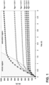
- FIG. 1 the output characteristics of an exemplary power MOSFET are shown, with the drain-source current (I DS ) depicted on the y-axis and the drain-source voltage (V DS ) depicted on the x-axis.
- I DS drain-source current
- V DS drain-source voltage
- the relationship between drain-source current (I DS ) and drain source voltage (V DS ) follows Ohm's law, in that the drain-source current (I DS ) is linearly proportional to the drain-source voltage (V DS ). For this reason, the Ohmic region of the power MOSFET is often referred to as "linear mode.”
- the drain-source current (I DS ) is nearly independent of the drain-source voltage (V DS ) and instead depends heavily on the gate voltage (V GS ). Stated differently, the load current (I DS ) first increases as the load path voltage (V DS ) increases in the Ohmic region, and then increases only slightly or less than proportionally as the load path voltage (V DS ) increases in the saturation region. The point at which saturation begins is higher for higher control voltages (V GS ), for example 100A for a 2.9V control voltage and 800A for a 4V control voltage.
- V GS gate voltage
- PWM pulse-width-modulated
- the control circuit includes a resistive load 10, and in particular, a resistive heating element, that is series connected between a 16V power supply 12 and the drain terminal of a power MOSFET 14.
- the MOSFET source terminal is connected to a shunt resistor 16 for measuring the drain source current (I DS ), which is also the current through the resistive load 10.
- I DS drain source current
- a further shunt resistor 18 is illustrated as being series connected between the power supply 12 and the resistive load 10 for measuring the power output of the power supply 12.
- the gate voltage (V GS ) of the power MOSFET 14 is controlled by actuation of first and second switch elements Q1, Q2, which are depicted as BJT transistors, but can include other switching elements in other embodiments.
- first and second switch elements Q1, Q2 cause the power MOSFET 14 to receive a gate voltage (V GS ) having a desired duty cycle and a desired frequency.
- DC power supply 20 is selectively coupled to the gate terminal of the MOSFET 14 when switching element Q2 is closed, which is in turn responsive to actuation of switching element Q1.
- Switching element Q1 is voltage controlled based on the output of power supply 22, which is optionally microcontroller-controlled. Because the power MOSFET 14 includes short switching times through its Ohmic region, millisecond duty cycle control of the gate voltage (V GS ) is possible in the linear mode, regardless of the load.
- the method includes activating the power MOSFET 14 with a pulse-width-modulated (PWM) gate voltage (V GS ) at a baseline frequency (e.g., 100 kHz) and duty cycle (e.g., 0.02).
- PWM pulse-width-modulated
- the method includes measuring the current (I DS ) in the load path.
- this measurement is performed by measuring the voltage across the shunt resistor 16, which as noted above is series-connected to the resistive load 10.
- the measured current (I DS ) is compared with a current limit value (I DS-Limit ). If the measured current (I DS ) is not less than the current limit value (I DS-Limit ), the method includes maintaining the frequency ( f ) and the duty cycle ( D ) of the pulse-width-modulated gate voltage (V GS ) at step 46.
- the method includes iteratively decreasing (decrementing) the frequency ( f ) and iteratively increasing (incrementing) the duty cycle ( D ).
- the frequency ( f ) can be reduced in 2 kHz decrements to 98 kHz at step 48, and the load current (I DS ) measured at step 50. If the current limit value (I DS-Limit ) is met at decision step 52, the method includes returning to the immediately preceding frequency at step 54.
- the duty cycle is increased at step 56, optionally in increments of 0.02 to a duty cycle ( D ) of 0.04.
- the load current (I DS ) is again measured at step 58 and compared with the current limit value (I DS-Limit ) at decision step 60. If the current limit value (I DS-Limit ) is not met, the frequency ( f ) and duty cycle ( D ) is again iteratively increased at step 48, and the load current (I DS ) is measured at step 50.
- the method includes returning to the immediately preceding duty cycle at step 62.
- the gate voltage is a digital output provided by a controller, for example a proportional-integral-derivative controller.
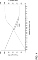
- the frequency ( f ) and duty cycle ( D ) of the gate voltage (V GS ) are plotted as a function of the heat mat current (I DS ) in Figure 4 .
- the pulse-width-modulated gate voltage (V GS ) includes a frequency (solid line) that decreases from 100 kHz to approximately 30 kHz, with a corresponding increase in heat mat current.
- the pulse-width-modulated gate voltage (V GS ) includes a duty cycle (broken line) that increases from zero to approximately unity, with a corresponding increase in heat mat current.
- the linear operating mode of the power MOSFET is shown in Figure 4 as being between 4A and 6.5A.
- the current limit value (I DS-Limit ) is selected to be approximately 6A in this example, ensuring that the power MOSFET operates in its Ohmic region with a gate voltage frequency of between 30 kHz and 50 kHz and a duty cycle (pulse width %) of between 0.3 and 0.6.
- the drain-source voltage (V DS ) and drain-source current (I DS ) for the circuit of Figure 2 are plotted as a function of time in Figure 5 . In this simulation, drain-source current (I DS ) gradually increases from zero (as the gate voltage duty cycle increases from zero) to a maximum of 8A, while the drain source voltage (V DS ) decreases over the same time interval.
- Laboratory testing revealed the ability of the system and method of the present invention to reduce electromagnetic interference.
- electromagnetic emissions were evaluated during turn on and turn off a 7A heat mat.
- the detected emissions were found to be only 77% of ICNIRP guidelines for time-varying electromagnetic fields.
- the detected emissions were found to be only 65% of ICNIRP guidelines for time-varying electromagnetic fields.
- the present system and method was also determined to reduce the start-up current for the heat mat at lower temperatures, resulting in more flexibility for the heat mat.
- the load current rate of change (di/dt) is monitored by the controller as the load current load current (I DS ) gradually increased to the current limit value (I DS-Limit ).
- the load current rate of change (di/dt) is maintained below a predetermined threshold that is stored to computer readable memory, and by extension, the rate of change of the load path voltage (V DS ) is also kept below a predetermined threshold.
- the load current rate of change (di/dt) is monitored through the shunt resistor 16.
- a controller interprets this condition as the transition point between the linear mode and the saturation mode.
- the controller varies the PWM gate voltage (V GS ) and iteratively identifies a range of PWM control voltages for the given load, at which the rate of change in current (di/dt) stays positive (above the threshold) throughout activation of the power MOSFET.
- the gate voltage is between 0 and 2.9V, with a duty cycle between .2 and .8 and a frequency between 20 and 80 kHz. As shown in Figure 4 , for example, a frequency of between about 40 and 60 kHz provided up to 7 A of current to the heat mat, with operation of the MOSFET only in the linear mode.
- the electromagnetic field of the series-connected heat mat was found to be significantly lower by operating the power MOSFET in its linear mode. Because the present method operates iteratively, it is uniquely adapted to dynamically determine the MOSFET's linear mode for a given resistive load, without prior knowledge of the load itself. As a consequence, the present invention can be implemented in combination with a wide variety of heat mats. For example, a universal power supply module can provide EMI-mitigation to a wide range of heat mats by internally calibrating its power MOSFET during regular operation.
- the resistive element can extend in a serpentine pattern in a first direction, and can extend in the same serpentine pattern in a second direction, opposite of the first direction, such that the magnetic field generated by the resistive element is self-canceling.
- the resistive element can double-back within the heat mat, such that at any given point along the serpentine winding, two sections of the resistive element are situated side-by-side.
- the magnetic field generated by the DC current in a first direction is canceled by the magnetic field generated by the DC current in a second, opposite direction.
- the EMI generated by the heat mat is reduced at the load, rather than range of heat mats by internally calibrating its power MOSFET during regular operation.
- the resistive element can extend in a serpentine pattern in a first direction, and can extend in the same serpentine pattern in a second direction, opposite of the first direction, such that the magnetic field generated by the resistive element is self-canceling.
- the resistive element can double-back within the heat mat, such that at any given point along the serpentine winding, two sections of the resistive element are situated side-by-side.
- the magnetic field generated by the DC current in a first direction is canceled by the magnetic field generated by the DC current in a second, opposite direction.
- the EMI generated by the heat mat is reduced at the load, rather than by operation of the power MOSFET in linear mode.
- the heat mat manufactured according to this construction can be used with a power MOSFET in linear mode to further reduce EMI from the heat mat.
Landscapes
- Engineering & Computer Science (AREA)
- Power Engineering (AREA)
- Aviation & Aerospace Engineering (AREA)
- Transportation (AREA)
- Mechanical Engineering (AREA)
- Physics & Mathematics (AREA)
- Electromagnetism (AREA)
- Control Of Voltage And Current In General (AREA)
- Electronic Switches (AREA)
- Control Of Electrical Variables (AREA)
Description
- The present invention relates to the operation of power MOSFETs in switching applications to reduce emissions and interference from electromagnetic fields, optionally for use in temperature-controlled vehicle seats. The present invention can also reduce the inrush current or starting current for capacitive and inductive loads, providing cost savings for switching operatons.
- Electric seat heaters for motor vehicles include a heat mat for converting electrical energy into heat. The heat mat includes a resistive heating element that is positioned close to the trim cover, often in a serpentine pattern. Modern heat mats are characterized by a short warm-up phase and an even distribution of heat for providing comfort in cold weather conditions and over long distance driving.
- Heat mats are typically controlled by a power MOSFET. The power MOSFET provides a pulse-width-modulated drain source current (IDS) for regulating the thermal output of the seat mat. However, when heat mats are energized, the electromagnetic emissions or interference can be undesirably high, sometimes exceeding International Commission on Non-Ionizing Radiation Protection (ICNIRP) guidelines for time-varying electromagnetic fields. Since the resistance of the heat mat varies with temperature, the electromagnetic emissions can be especially problematic at lower temperatures, when the het mat resistance is lowered. Reference may be made to
US 5 550 702 A which relates to adaptive duty-cycle limiting for overload protection of integrated circuits. Reference may be made toKR 101 642 761 B1 EP 1 489 730 A2WO 2019/121216 A1 which relates to a switching circuit. - Accordingly, there remains a continued need for a system and a method for regulating power to a heat mat, or other resistive load, to minimize the resulting electromagnetic field, particularly during turn-on and turn-off of the resistive load.
- The present invention is defined by the appended claims, to which reference should now be made. Specific embodiments are defined in the dependent claims. A system and a method for controlling a power MOSFET for limiting electromagnetic emissions and interference from a load is provided. The system and method include a pulse-width-modulated (PWM) control voltage to operate the power MOSFET in accordance with its Ohmic region (linear mode). By operating the power MOSFET in its Ohmic region, the electromagnetic field generated by the load is reduced, without requiring a dedicated DC/DC converter that would otherwise increase the cost, size, and weight of the electronic control module.
- A control circuit includes a power MOSFET and a resistive load, for example a heat mat. The power MOSFET includes a gate terminal connected to a PWM gate voltage (VGS) for controlling current through the power MOSFET, which is series connected to the heat mat. The frequency and the duty cycle of the PWM gate voltage (VGS) are iteratively selected such that the power MOSFET operates only in its Ohmic region, as optionally measured by the rate of change of current (di/dt) through a shunt resistor, for example. Further the present invention can control the rate of change of current (di/dt) and rate or change of voltage (dv/dt) for the resistive load. For example, a universal power supply module can provide electromagnetic interference mitigation for a wide range of heat mats by internally calibrating its power MOSFET control voltage without special knowledge of the heat mats. Additional embodiments include winding the heater coil in a first direction and in a second, opposite direction, such that the magnetic field is canceled along the length of the heater coil.
- These and other features and advantages of the present invention will become apparent from the following description of the invention, when viewed in accordance with the accompanying drawings and the appended claim.
-
-
Figure 1 is an operating area diagram depicting the output characteristics of a power MOSFET, including an Ohmic (linear) region and a saturation region. -
Figure 2 is a circuit diagram including a frequency (f) and duty cycle (D) controlled power MOSFET for mitigating electromagnetic interference from a resistive load. -
Figure 3 is a flow chart illustrating frequency (f) and duty cycle (D) control of a power MOSFET for mitigating electromagnetic interference from a resistive load. -
Figure 4 is a graph illustrating the gate voltage (VGS) frequency (f) and duty cycle (D) as a function of the heat mat current (IDS). -
Figure 5 is a graph that illustrating the drain-source voltage (VDS) and drain-source current (IDS) as a function of time. - In the present embodiment, a power MOSFET is used as a switch to control the flow of power to an electrical load, and in particular, a resistive heating element for an electric seat heater. As is known in the art, a MOSFET is a three-terminal device in which the gate voltage controls the flow of current between a source and a drain. The system and method of the present invention limit electromagnetic emissions and interference from the electric seat heater by operating the power MOSFET in its Ohmic region. Before the system and the method are discussed in greater detail, general operation of a power MOSFET in its Ohmic region will now be described.
- Referring to
Figure 1 , the output characteristics of an exemplary power MOSFET are shown, with the drain-source current (IDS) depicted on the y-axis and the drain-source voltage (VDS) depicted on the x-axis. In the Ohmic region (at left), the relationship between drain-source current (IDS) and drain source voltage (VDS) follows Ohm's law, in that the drain-source current (IDS) is linearly proportional to the drain-source voltage (VDS). For this reason, the Ohmic region of the power MOSFET is often referred to as "linear mode." - In the saturation region (at right), the drain-source current (IDS) is nearly independent of the drain-source voltage (VDS) and instead depends heavily on the gate voltage (VGS). Stated differently, the load current (IDS) first increases as the load path voltage (VDS) increases in the Ohmic region, and then increases only slightly or less than proportionally as the load path voltage (VDS) increases in the saturation region. The point at which saturation begins is higher for higher control voltages (VGS), for example 100A for a 2.9V control voltage and 800A for a 4V control voltage. In order to reduce electromagnetic interference (EMI) in the load, it is desirable to operate the MOSFET only in its linear mode (Ohmic region) or at the transition between the Ohmic region and the saturation region. As set forth in Part II below, this is achieved by controlling the gate voltage (VGS) duty cycle and frequency. The gate voltage (VGS) is, for example, a pulse-width-modulated (PWM) signal, such that the frequency and duration of the individual control pulses and the time interval between two successive pulses can vary.
- Referring now to
Figure 2 , a control circuit for mitigating EMI by operating a power MOSFET substantially in its Ohmic region is illustrated. The control circuit includes aresistive load 10, and in particular, a resistive heating element, that is series connected between a16V power supply 12 and the drain terminal of apower MOSFET 14. The MOSFET source terminal is connected to ashunt resistor 16 for measuring the drain source current (IDS), which is also the current through theresistive load 10. Afurther shunt resistor 18 is illustrated as being series connected between thepower supply 12 and theresistive load 10 for measuring the power output of thepower supply 12. - As also shown in
Figure 2 , the gate voltage (VGS) of thepower MOSFET 14 is controlled by actuation of first and second switch elements Q1, Q2, which are depicted as BJT transistors, but can include other switching elements in other embodiments. In particular, first and second switch elements Q1, Q2 cause thepower MOSFET 14 to receive a gate voltage (VGS) having a desired duty cycle and a desired frequency.DC power supply 20 is selectively coupled to the gate terminal of theMOSFET 14 when switching element Q2 is closed, which is in turn responsive to actuation of switching element Q1. Switching element Q1 is voltage controlled based on the output ofpower supply 22, which is optionally microcontroller-controlled. Because thepower MOSFET 14 includes short switching times through its Ohmic region, millisecond duty cycle control of the gate voltage (VGS) is possible in the linear mode, regardless of the load. - Operation of the control circuit of
Figure 2 is illustrated in connection with the functional block diagram ofFigure 3 . As noted above, the gate voltage (VGS) duty cycle (D), which is the ratio of the MOSFET on duration to the switching time period, is varied, as is the gate voltage frequency (f). Atstep 40, the method includes activating thepower MOSFET 14 with a pulse-width-modulated (PWM) gate voltage (VGS) at a baseline frequency (e.g., 100 kHz) and duty cycle (e.g., 0.02). Atstep 42, the method includes measuring the current (IDS) in the load path. In the present embodiment, this measurement is performed by measuring the voltage across theshunt resistor 16, which as noted above is series-connected to theresistive load 10. At decision step 44, the measured current (IDS) is compared with a current limit value (IDS-Limit). If the measured current (IDS) is not less than the current limit value (IDS-Limit), the method includes maintaining the frequency (f) and the duty cycle (D) of the pulse-width-modulated gate voltage (VGS) atstep 46. If the measured current (IDS) is less than the current limit value (IDS-Limit), the method includes iteratively decreasing (decrementing) the frequency (f) and iteratively increasing (incrementing) the duty cycle (D). For example, the frequency (f) can be reduced in 2 kHz decrements to 98 kHz at step 48, and the load current (IDS) measured atstep 50. If the current limit value (IDS-Limit) is met atdecision step 52, the method includes returning to the immediately preceding frequency atstep 54. If the current limit value (IDS-Limit) is not met atdecision step 52, the duty cycle is increased atstep 56, optionally in increments of 0.02 to a duty cycle (D) of 0.04. The load current (IDS) is again measured atstep 58 and compared with the current limit value (IDS-Limit) atdecision step 60. If the current limit value (IDS-Limit) is not met, the frequency (f) and duty cycle (D) is again iteratively increased at step 48, and the load current (IDS) is measured atstep 50. If however the load current (IDS) is equal to or greater than the current limit value (IDS-Limit), the method includes returning to the immediately preceding duty cycle atstep 62. In other embodiments, the gate voltage is a digital output provided by a controller, for example a proportional-integral-derivative controller. - To further illustrate frequency and duty cycle control of the power MOSFET, the frequency (f) and duty cycle (D) of the gate voltage (VGS) are plotted as a function of the heat mat current (IDS) in
Figure 4 . As shown inFigure 4 , the pulse-width-modulated gate voltage (VGS) includes a frequency (solid line) that decreases from 100 kHz to approximately 30 kHz, with a corresponding increase in heat mat current. Interleaved with this decrease in frequency, the pulse-width-modulated gate voltage (VGS) includes a duty cycle (broken line) that increases from zero to approximately unity, with a corresponding increase in heat mat current. The linear operating mode of the power MOSFET is shown inFigure 4 as being between 4A and 6.5A. The current limit value (IDS-Limit) is selected to be approximately 6A in this example, ensuring that the power MOSFET operates in its Ohmic region with a gate voltage frequency of between 30 kHz and 50 kHz and a duty cycle (pulse width %) of between 0.3 and 0.6. The drain-source voltage (VDS) and drain-source current (IDS) for the circuit ofFigure 2 are plotted as a function of time inFigure 5 . In this simulation, drain-source current (IDS) gradually increases from zero (as the gate voltage duty cycle increases from zero) to a maximum of 8A, while the drain source voltage (VDS) decreases over the same time interval. - Laboratory testing revealed the ability of the system and method of the present invention to reduce electromagnetic interference. In particular, electromagnetic emissions were evaluated during turn on and turn off a 7A heat mat. During turn on, the detected emissions were found to be only 77% of ICNIRP guidelines for time-varying electromagnetic fields. During turn off, the detected emissions were found to be only 65% of ICNIRP guidelines for time-varying electromagnetic fields. The present system and method was also determined to reduce the start-up current for the heat mat at lower temperatures, resulting in more flexibility for the heat mat.
- In the foregoing mode of operation, the load current rate of change (di/dt) is monitored by the controller as the load current load current (IDS) gradually increased to the current limit value (IDS-Limit). The load current rate of change (di/dt) is maintained below a predetermined threshold that is stored to computer readable memory, and by extension, the rate of change of the load path voltage (VDS) is also kept below a predetermined threshold. As an alternative mode of operation, the load current rate of change (di/dt) is monitored through the
shunt resistor 16. As the rate of change in current (di/dt) slows, i.e., as di/dt falls below a threshold while the gate voltage (VGS) increases, a controller (not shown) interprets this condition as the transition point between the linear mode and the saturation mode. In this case, the controller varies the PWM gate voltage (VGS) and iteratively identifies a range of PWM control voltages for the given load, at which the rate of change in current (di/dt) stays positive (above the threshold) throughout activation of the power MOSFET. In various embodiments, the gate voltage is between 0 and 2.9V, with a duty cycle between .2 and .8 and a frequency between 20 and 80 kHz. As shown inFigure 4 , for example, a frequency of between about 40 and 60 kHz provided up to 7 A of current to the heat mat, with operation of the MOSFET only in the linear mode. - As noted above, the electromagnetic field of the series-connected heat mat was found to be significantly lower by operating the power MOSFET in its linear mode. Because the present method operates iteratively, it is uniquely adapted to dynamically determine the MOSFET's linear mode for a given resistive load, without prior knowledge of the load itself. As a consequence, the present invention can be implemented in combination with a wide variety of heat mats. For example, a universal power supply module can provide EMI-mitigation to a wide range of heat mats by internally calibrating its power MOSFET during regular operation.
- As an alternative solution, the resistive element can extend in a serpentine pattern in a first direction, and can extend in the same serpentine pattern in a second direction, opposite of the first direction, such that the magnetic field generated by the resistive element is self-canceling. Stated differently, the resistive element can double-back within the heat mat, such that at any given point along the serpentine winding, two sections of the resistive element are situated side-by-side. As a result, the magnetic field generated by the DC current in a first direction is canceled by the magnetic field generated by the DC current in a second, opposite direction. In this respect, the EMI generated by the heat mat is reduced at the load, rather than range of heat mats by internally calibrating its power MOSFET during regular operation.
- As an alternative solution, the resistive element can extend in a serpentine pattern in a first direction, and can extend in the same serpentine pattern in a second direction, opposite of the first direction, such that the magnetic field generated by the resistive element is self-canceling. Stated differently, the resistive element can double-back within the heat mat, such that at any given point along the serpentine winding, two sections of the resistive element are situated side-by-side. As a result, the magnetic field generated by the DC current in a first direction is canceled by the magnetic field generated by the DC current in a second, opposite direction. In this respect, the EMI generated by the heat mat is reduced at the load, rather than by operation of the power MOSFET in linear mode. In still further embodiments, the heat mat manufactured according to this construction can be used with a power MOSFET in linear mode to further reduce EMI from the heat mat.
- The above description is that of a current embodiment of the invention. Various alterations and changes can be made without departing from broader aspects of the invention, as defined by the appended claims.
Claims (14)
- A method for pulse-width-modulated, PWM, control of a power MOSFET having a load path, the method comprising:a) providing an electrical load that is series connected with the load path of the power MOSFET;b) activating (40) the power MOSFET with a PWM gate voltage, the PWM gate voltage having a frequency and a duty cycle;c) measuring (42) the current in the load path of the power MOSFET during activation of the power MOSFET;d) comparing (44) the measured current in the load path of the power MOSFET with a current limit value; ande) iteratively decreasing a frequency of the PWM gate voltage and increasing a duty cycle of the PWM gate voltage until the measured current in the load path is determined to exceed the current limit value, measuring the current in the load path after each gate voltage modification, and reverting (54, 62) to an immediately previous frequency or duty cycle of the PWM gate voltage if the measured current is not less than the current limit value.
- The method of claim 1 wherein the electrical load is a resistive element of an electric seat heater.
- The method of claim 1 wherein the electrical load is coupled to a drain terminal or a source terminal of the power MOSFET.
- The method of claim 1 further including a capacitor coupled in parallel between a gate terminal and a source terminal of the power MOSFET.
- The method of claim 1 wherein the varying the frequency and the duty cycle of the PWM gate voltage includes alternately reducing the frequency of the PWM gate voltage and increasing the duty cycle of the PWM gate voltage.
- The method of claim 1 wherein steps b) through e) are performed by a proportional-integral-derivative controller or with reference to a look-up table stored to memory.
- A system for pulse-width-modulated, PWM, control of a power MOSFET, the system comprising:a power MOSFET (14) having a load path;an electrical load (10) that is series connected with the load path of the power MOSFET (14);a current sensor (16) adapted to measure a current value in the load path of the power MOSFET (14);a voltage source (22) adapted to provide a variable PWM gate voltage to the power MOSFET, wherein the voltage source (22) is operable to iteratively decrease a frequency of the PWM gate voltage and iteratively increase a duty cycle of the PWM gate voltage until a measured current in the load path is determined to exceed a current limit value based on the output of the current sensor (16).
- The system of claim 7 wherein the electrical load (10) is a resistive element of an electric seat heater.
- The system of claim 7 wherein the voltage source (22) includes at least one microcontroller-controlled switching element.
- The system of claim 7 wherein the voltage source (22) includes a proportional-integral-derivative controller.
- The system of claim 7 further including a capacitor coupled in parallel between a gate terminal and a source terminal of the power MOSFET (14).
- The system of claim 7 wherein the frequency of the PWM gate voltage is between 20 kHz and 80 kHz and wherein the duty cycle of the PWM gate voltage is between 0.2 and 0.8.
- The system of claim 7 wherein the electrical load (10) is coupled to a drain terminal or a source terminal of the power MOSFET (14).
- The system of claim 7 wherein the electrical load (10) includes a capacitive element or an inductive element.
Applications Claiming Priority (2)
| Application Number | Priority Date | Filing Date | Title |
|---|---|---|---|
| US201962882001P | 2019-08-02 | 2019-08-02 | |
| PCT/IB2020/057272 WO2021024134A1 (en) | 2019-08-02 | 2020-07-31 | Method for reducing magnetic field emission for heated seats and other applications |
Publications (2)
| Publication Number | Publication Date |
|---|---|
| EP4008045A1 EP4008045A1 (en) | 2022-06-08 |
| EP4008045B1 true EP4008045B1 (en) | 2025-06-18 |
Family
ID=72046955
Family Applications (1)
| Application Number | Title | Priority Date | Filing Date |
|---|---|---|---|
| EP20754374.5A Active EP4008045B1 (en) | 2019-08-02 | 2020-07-31 | Method for reducing magnetic field emission for heated seats and other applications |
Country Status (5)
| Country | Link |
|---|---|
| US (1) | US12490344B2 (en) |
| EP (1) | EP4008045B1 (en) |
| CN (1) | CN114223119B (en) |
| ES (1) | ES3038082T3 (en) |
| WO (1) | WO2021024134A1 (en) |
Families Citing this family (4)
| Publication number | Priority date | Publication date | Assignee | Title |
|---|---|---|---|---|
| WO2021024134A1 (en) * | 2019-08-02 | 2021-02-11 | HELLA GmbH & Co. KGaA | Method for reducing magnetic field emission for heated seats and other applications |
| US20230253783A1 (en) * | 2020-07-31 | 2023-08-10 | HELLA GmbH & Co. KGaA | Method for reducing in-rush currents in battery charging applications |
| US11870428B1 (en) * | 2022-08-26 | 2024-01-09 | Infineon Technologies Austria Ag | System and method for pulsed gate control of a transistor |
| EP4734656A1 (en) * | 2024-10-24 | 2026-04-29 | Mahle International GmbH | Method for operating a ptc heater |
Citations (4)
| Publication number | Priority date | Publication date | Assignee | Title |
|---|---|---|---|---|
| US5550702A (en) * | 1994-11-21 | 1996-08-27 | Texas Instruments Incorporated | Adaptive duty-cycle limiting for overload protection of integrated circuits |
| EP1489730A2 (en) * | 2001-05-22 | 2004-12-22 | Powerdsine Limited | Power distribution with digital current control |
| KR101642761B1 (en) * | 2015-01-22 | 2016-08-10 | 주식회사 동운아나텍 | Soft start apparatus and method for dc-dc converter |
| WO2019121216A1 (en) * | 2017-12-18 | 2019-06-27 | Safran Electronics & Defense | Switching circuit |
Family Cites Families (9)
| Publication number | Priority date | Publication date | Assignee | Title |
|---|---|---|---|---|
| EP1261119A3 (en) * | 2001-05-22 | 2003-11-12 | Powerdsine Limited | Power factor corrector with efficient ripple attenuator |
| CN102545567B (en) * | 2010-12-08 | 2014-07-30 | 昂宝电子(上海)有限公司 | Systems and methods for providing overcurrent protection for power converters |
| US9553501B2 (en) * | 2010-12-08 | 2017-01-24 | On-Bright Electronics (Shanghai) Co., Ltd. | System and method providing over current protection based on duty cycle information for power converter |
| DE102012015787B3 (en) | 2012-08-08 | 2013-12-12 | Fairchild Semiconductor Corp. | Gate driver for driving gate of switch, has control input for receiving control signal, where amplified output signal is provided by output for controlling gate of switch, while control device is connected between control input and output |
| CN105027443B (en) | 2013-03-09 | 2018-12-11 | 密克罗奇普技术公司 | Inductive Load Driver Slew Rate Controller |
| CN104660022B (en) * | 2015-02-02 | 2017-06-13 | 昂宝电子(上海)有限公司 | The system and method that overcurrent protection is provided for supply convertor |
| CN107482610A (en) | 2017-07-28 | 2017-12-15 | 浙江大学 | A kind of submarine observation network constant-current supply system based on adjustable duty cycle power balancer |
| WO2021024134A1 (en) * | 2019-08-02 | 2021-02-11 | HELLA GmbH & Co. KGaA | Method for reducing magnetic field emission for heated seats and other applications |
| US20230253783A1 (en) * | 2020-07-31 | 2023-08-10 | HELLA GmbH & Co. KGaA | Method for reducing in-rush currents in battery charging applications |
-
2020
- 2020-07-31 WO PCT/IB2020/057272 patent/WO2021024134A1/en not_active Ceased
- 2020-07-31 ES ES20754374T patent/ES3038082T3/en active Active
- 2020-07-31 EP EP20754374.5A patent/EP4008045B1/en active Active
- 2020-07-31 CN CN202080054337.4A patent/CN114223119B/en active Active
- 2020-07-31 US US17/630,603 patent/US12490344B2/en active Active
Patent Citations (4)
| Publication number | Priority date | Publication date | Assignee | Title |
|---|---|---|---|---|
| US5550702A (en) * | 1994-11-21 | 1996-08-27 | Texas Instruments Incorporated | Adaptive duty-cycle limiting for overload protection of integrated circuits |
| EP1489730A2 (en) * | 2001-05-22 | 2004-12-22 | Powerdsine Limited | Power distribution with digital current control |
| KR101642761B1 (en) * | 2015-01-22 | 2016-08-10 | 주식회사 동운아나텍 | Soft start apparatus and method for dc-dc converter |
| WO2019121216A1 (en) * | 2017-12-18 | 2019-06-27 | Safran Electronics & Defense | Switching circuit |
Also Published As
| Publication number | Publication date |
|---|---|
| WO2021024134A1 (en) | 2021-02-11 |
| EP4008045A1 (en) | 2022-06-08 |
| ES3038082T3 (en) | 2025-10-09 |
| US20220256651A1 (en) | 2022-08-11 |
| CN114223119A (en) | 2022-03-22 |
| CN114223119B (en) | 2026-04-24 |
| US12490344B2 (en) | 2025-12-02 |
Similar Documents
| Publication | Publication Date | Title |
|---|---|---|
| EP4008045B1 (en) | Method for reducing magnetic field emission for heated seats and other applications | |
| CN110971176B (en) | Driver device | |
| EP2668818B1 (en) | Electrical heater, vehicle having an electrical heater and method for controlling an electrical heater | |
| CN105281571B (en) | For the controllable conduction time reduction with the regulator of PFM mode operations | |
| EP3404790B1 (en) | Power supply control device | |
| US8947064B2 (en) | System and method for driving an electronic switch dependent on temperature | |
| US10122254B2 (en) | Devices, systems and processes for average current control | |
| CN111356251B (en) | Method for operating an electric heater | |
| US10135437B2 (en) | Drive control apparatus | |
| US20210184486A1 (en) | Pre-charging circuit and pre-charging method | |
| CN107408884B (en) | Power conversion device and control method for power conversion device | |
| KR20240057349A (en) | Adaptive pre-charge control for electric vehicle dc link capacitor | |
| US20230088339A1 (en) | Method for reducing oscillation during turn on of a power transistor by regulating the gate switching speed control of its complementary power transistor | |
| US20230170790A1 (en) | Method of safely discharging dc link capacitor of multiple phase inverter | |
| CA3140388A1 (en) | Load control device having a closed-loop gate drive circuit | |
| US12614902B2 (en) | Intelligent semiconductor switch | |
| KR20180073636A (en) | Method for controlling the current of an inductive load | |
| CN112752959B (en) | Temperature measurement of power semiconductor switching elements | |
| CN103633972A (en) | Method and device for power controlling or voltage controlling of an electric load device | |
| CN110806767B (en) | Heating device and its temperature control circuit and temperature control method | |
| Laumen et al. | Closed-loop dv/dt control of SiC MOSFETs yielding minimal losses and machine degradation | |
| KR102295580B1 (en) | Controlling apparatus and method for senscing ovecurrent of dc motor for vehicle | |
| CN103715888B (en) | Method for reducing power loss in circuits driving inductive loads | |
| US8525367B2 (en) | Control unit and method for controlling passenger-protection means for a vehicle | |
| EP2704166A1 (en) | Adaptive current control for inductive loads |
Legal Events
| Date | Code | Title | Description |
|---|---|---|---|
| STAA | Information on the status of an ep patent application or granted ep patent |
Free format text: STATUS: UNKNOWN |
|
| STAA | Information on the status of an ep patent application or granted ep patent |
Free format text: STATUS: THE INTERNATIONAL PUBLICATION HAS BEEN MADE |
|
| PUAI | Public reference made under article 153(3) epc to a published international application that has entered the european phase |
Free format text: ORIGINAL CODE: 0009012 |
|
| STAA | Information on the status of an ep patent application or granted ep patent |
Free format text: STATUS: REQUEST FOR EXAMINATION WAS MADE |
|
| 17P | Request for examination filed |
Effective date: 20220128 |
|
| AK | Designated contracting states |
Kind code of ref document: A1 Designated state(s): AL AT BE BG CH CY CZ DE DK EE ES FI FR GB GR HR HU IE IS IT LI LT LU LV MC MK MT NL NO PL PT RO RS SE SI SK SM TR |
|
| DAV | Request for validation of the european patent (deleted) | ||
| DAX | Request for extension of the european patent (deleted) | ||
| STAA | Information on the status of an ep patent application or granted ep patent |
Free format text: STATUS: EXAMINATION IS IN PROGRESS |
|
| 17Q | First examination report despatched |
Effective date: 20240625 |
|
| GRAP | Despatch of communication of intention to grant a patent |
Free format text: ORIGINAL CODE: EPIDOSNIGR1 |
|
| STAA | Information on the status of an ep patent application or granted ep patent |
Free format text: STATUS: GRANT OF PATENT IS INTENDED |
|
| INTG | Intention to grant announced |
Effective date: 20250130 |
|
| GRAS | Grant fee paid |
Free format text: ORIGINAL CODE: EPIDOSNIGR3 |
|
| GRAA | (expected) grant |
Free format text: ORIGINAL CODE: 0009210 |
|
| STAA | Information on the status of an ep patent application or granted ep patent |
Free format text: STATUS: THE PATENT HAS BEEN GRANTED |
|
| AK | Designated contracting states |
Kind code of ref document: B1 Designated state(s): AL AT BE BG CH CY CZ DE DK EE ES FI FR GB GR HR HU IE IS IT LI LT LU LV MC MK MT NL NO PL PT RO RS SE SI SK SM TR |
|
| REG | Reference to a national code |
Ref country code: GB Ref legal event code: FG4D |
|
| REG | Reference to a national code |
Ref country code: CH Ref legal event code: EP |
|
| REG | Reference to a national code |
Ref country code: DE Ref legal event code: R096 Ref document number: 602020052945 Country of ref document: DE |
|
| REG | Reference to a national code |
Ref country code: CH Ref legal event code: EP |
|
| REG | Reference to a national code |
Ref country code: IE Ref legal event code: FG4D |
|
| PGFP | Annual fee paid to national office [announced via postgrant information from national office to epo] |
Ref country code: FR Payment date: 20250623 Year of fee payment: 6 |
|
| PG25 | Lapsed in a contracting state [announced via postgrant information from national office to epo] |
Ref country code: FI Free format text: LAPSE BECAUSE OF FAILURE TO SUBMIT A TRANSLATION OF THE DESCRIPTION OR TO PAY THE FEE WITHIN THE PRESCRIBED TIME-LIMIT Effective date: 20250618 |
|
| PGFP | Annual fee paid to national office [announced via postgrant information from national office to epo] |
Ref country code: ES Payment date: 20250807 Year of fee payment: 6 |
|
| REG | Reference to a national code |
Ref country code: ES Ref legal event code: FG2A Ref document number: 3038082 Country of ref document: ES Kind code of ref document: T3 Effective date: 20251009 |
|
| PGFP | Annual fee paid to national office [announced via postgrant information from national office to epo] |
Ref country code: DE Payment date: 20250618 Year of fee payment: 6 |
|
| REG | Reference to a national code |
Ref country code: LT Ref legal event code: MG9D |
|
| PG25 | Lapsed in a contracting state [announced via postgrant information from national office to epo] |
Ref country code: GR Free format text: LAPSE BECAUSE OF FAILURE TO SUBMIT A TRANSLATION OF THE DESCRIPTION OR TO PAY THE FEE WITHIN THE PRESCRIBED TIME-LIMIT Effective date: 20250919 Ref country code: NO Free format text: LAPSE BECAUSE OF FAILURE TO SUBMIT A TRANSLATION OF THE DESCRIPTION OR TO PAY THE FEE WITHIN THE PRESCRIBED TIME-LIMIT Effective date: 20250918 |
|
| PG25 | Lapsed in a contracting state [announced via postgrant information from national office to epo] |
Ref country code: BG Free format text: LAPSE BECAUSE OF FAILURE TO SUBMIT A TRANSLATION OF THE DESCRIPTION OR TO PAY THE FEE WITHIN THE PRESCRIBED TIME-LIMIT Effective date: 20250618 |
|
| PG25 | Lapsed in a contracting state [announced via postgrant information from national office to epo] |
Ref country code: HR Free format text: LAPSE BECAUSE OF FAILURE TO SUBMIT A TRANSLATION OF THE DESCRIPTION OR TO PAY THE FEE WITHIN THE PRESCRIBED TIME-LIMIT Effective date: 20250618 |
|
| PG25 | Lapsed in a contracting state [announced via postgrant information from national office to epo] |
Ref country code: RS Free format text: LAPSE BECAUSE OF FAILURE TO SUBMIT A TRANSLATION OF THE DESCRIPTION OR TO PAY THE FEE WITHIN THE PRESCRIBED TIME-LIMIT Effective date: 20250918 |
|
| REG | Reference to a national code |
Ref country code: NL Ref legal event code: MP Effective date: 20250618 |
|
| PG25 | Lapsed in a contracting state [announced via postgrant information from national office to epo] |
Ref country code: LV Free format text: LAPSE BECAUSE OF FAILURE TO SUBMIT A TRANSLATION OF THE DESCRIPTION OR TO PAY THE FEE WITHIN THE PRESCRIBED TIME-LIMIT Effective date: 20250618 |
|
| PG25 | Lapsed in a contracting state [announced via postgrant information from national office to epo] |
Ref country code: NL Free format text: LAPSE BECAUSE OF FAILURE TO SUBMIT A TRANSLATION OF THE DESCRIPTION OR TO PAY THE FEE WITHIN THE PRESCRIBED TIME-LIMIT Effective date: 20250618 |
|
| PG25 | Lapsed in a contracting state [announced via postgrant information from national office to epo] |
Ref country code: PT Free format text: LAPSE BECAUSE OF FAILURE TO SUBMIT A TRANSLATION OF THE DESCRIPTION OR TO PAY THE FEE WITHIN THE PRESCRIBED TIME-LIMIT Effective date: 20251020 |
|
| REG | Reference to a national code |
Ref country code: AT Ref legal event code: MK05 Ref document number: 1805124 Country of ref document: AT Kind code of ref document: T Effective date: 20250618 |
|
| PG25 | Lapsed in a contracting state [announced via postgrant information from national office to epo] |
Ref country code: IS Free format text: LAPSE BECAUSE OF FAILURE TO SUBMIT A TRANSLATION OF THE DESCRIPTION OR TO PAY THE FEE WITHIN THE PRESCRIBED TIME-LIMIT Effective date: 20251018 |
|
| PG25 | Lapsed in a contracting state [announced via postgrant information from national office to epo] |
Ref country code: AT Free format text: LAPSE BECAUSE OF FAILURE TO SUBMIT A TRANSLATION OF THE DESCRIPTION OR TO PAY THE FEE WITHIN THE PRESCRIBED TIME-LIMIT Effective date: 20250618 Ref country code: SM Free format text: LAPSE BECAUSE OF FAILURE TO SUBMIT A TRANSLATION OF THE DESCRIPTION OR TO PAY THE FEE WITHIN THE PRESCRIBED TIME-LIMIT Effective date: 20250618 |
|
| PG25 | Lapsed in a contracting state [announced via postgrant information from national office to epo] |
Ref country code: CZ Free format text: LAPSE BECAUSE OF FAILURE TO SUBMIT A TRANSLATION OF THE DESCRIPTION OR TO PAY THE FEE WITHIN THE PRESCRIBED TIME-LIMIT Effective date: 20250618 |
|
| PG25 | Lapsed in a contracting state [announced via postgrant information from national office to epo] |
Ref country code: PL Free format text: LAPSE BECAUSE OF FAILURE TO SUBMIT A TRANSLATION OF THE DESCRIPTION OR TO PAY THE FEE WITHIN THE PRESCRIBED TIME-LIMIT Effective date: 20250618 |
|
| PG25 | Lapsed in a contracting state [announced via postgrant information from national office to epo] |
Ref country code: EE Free format text: LAPSE BECAUSE OF FAILURE TO SUBMIT A TRANSLATION OF THE DESCRIPTION OR TO PAY THE FEE WITHIN THE PRESCRIBED TIME-LIMIT Effective date: 20250618 |
|
| PG25 | Lapsed in a contracting state [announced via postgrant information from national office to epo] |
Ref country code: SK Free format text: LAPSE BECAUSE OF FAILURE TO SUBMIT A TRANSLATION OF THE DESCRIPTION OR TO PAY THE FEE WITHIN THE PRESCRIBED TIME-LIMIT Effective date: 20250618 Ref country code: RO Free format text: LAPSE BECAUSE OF FAILURE TO SUBMIT A TRANSLATION OF THE DESCRIPTION OR TO PAY THE FEE WITHIN THE PRESCRIBED TIME-LIMIT Effective date: 20250618 |
|
| REG | Reference to a national code |
Ref country code: CH Ref legal event code: H13 Free format text: ST27 STATUS EVENT CODE: U-0-0-H10-H13 (AS PROVIDED BY THE NATIONAL OFFICE) Effective date: 20260224 |
|
| PG25 | Lapsed in a contracting state [announced via postgrant information from national office to epo] |
Ref country code: LU Free format text: LAPSE BECAUSE OF NON-PAYMENT OF DUE FEES Effective date: 20250731 |
|
| REG | Reference to a national code |
Ref country code: DE Ref legal event code: R097 Ref document number: 602020052945 Country of ref document: DE |
|
| REG | Reference to a national code |
Ref country code: BE Ref legal event code: MM Effective date: 20250731 |
|
| PG25 | Lapsed in a contracting state [announced via postgrant information from national office to epo] |
Ref country code: MC Free format text: LAPSE BECAUSE OF FAILURE TO SUBMIT A TRANSLATION OF THE DESCRIPTION OR TO PAY THE FEE WITHIN THE PRESCRIBED TIME-LIMIT Effective date: 20250618 |
|
| PG25 | Lapsed in a contracting state [announced via postgrant information from national office to epo] |
Ref country code: DK Free format text: LAPSE BECAUSE OF FAILURE TO SUBMIT A TRANSLATION OF THE DESCRIPTION OR TO PAY THE FEE WITHIN THE PRESCRIBED TIME-LIMIT Effective date: 20250618 |
|
| PG25 | Lapsed in a contracting state [announced via postgrant information from national office to epo] |
Ref country code: BE Free format text: LAPSE BECAUSE OF NON-PAYMENT OF DUE FEES Effective date: 20250731 Ref country code: IT Free format text: LAPSE BECAUSE OF FAILURE TO SUBMIT A TRANSLATION OF THE DESCRIPTION OR TO PAY THE FEE WITHIN THE PRESCRIBED TIME-LIMIT Effective date: 20250618 |
|
| PG25 | Lapsed in a contracting state [announced via postgrant information from national office to epo] |
Ref country code: CH Free format text: LAPSE BECAUSE OF NON-PAYMENT OF DUE FEES Effective date: 20250731 |
|
| PLBE | No opposition filed within time limit |
Free format text: ORIGINAL CODE: 0009261 |
|
| STAA | Information on the status of an ep patent application or granted ep patent |
Free format text: STATUS: NO OPPOSITION FILED WITHIN TIME LIMIT |
|
| REG | Reference to a national code |
Ref country code: CH Ref legal event code: L10 Free format text: ST27 STATUS EVENT CODE: U-0-0-L10-L00 (AS PROVIDED BY THE NATIONAL OFFICE) Effective date: 20260430 |