EP4007462A1 - Method for manufacturing stack components - Google Patents
Method for manufacturing stack components Download PDFInfo
- Publication number
- EP4007462A1 EP4007462A1 EP19939888.4A EP19939888A EP4007462A1 EP 4007462 A1 EP4007462 A1 EP 4007462A1 EP 19939888 A EP19939888 A EP 19939888A EP 4007462 A1 EP4007462 A1 EP 4007462A1
- Authority
- EP
- European Patent Office
- Prior art keywords
- circuit layer
- circuit
- interposer
- stack component
- manufacturing
- Prior art date
- Legal status (The legal status is an assumption and is not a legal conclusion. Google has not performed a legal analysis and makes no representation as to the accuracy of the status listed.)
- Granted
Links
Images

Classifications
-
- H—ELECTRICITY
- H05—ELECTRIC TECHNIQUES NOT OTHERWISE PROVIDED FOR
- H05K—PRINTED CIRCUITS; CASINGS OR CONSTRUCTIONAL DETAILS OF ELECTRIC APPARATUS; MANUFACTURE OF ASSEMBLAGES OF ELECTRICAL COMPONENTS
- H05K3/00—Apparatus or processes for manufacturing printed circuits
- H05K3/46—Manufacturing multilayer circuits
- H05K3/4697—Manufacturing multilayer circuits having cavities, e.g. for mounting components
-
- B—PERFORMING OPERATIONS; TRANSPORTING
- B33—ADDITIVE MANUFACTURING TECHNOLOGY
- B33Y—ADDITIVE MANUFACTURING, i.e. MANUFACTURING OF THREE-DIMENSIONAL [3D] OBJECTS BY ADDITIVE DEPOSITION, ADDITIVE AGGLOMERATION OR ADDITIVE LAYERING, e.g. BY 3D PRINTING, STEREOLITHOGRAPHY OR SELECTIVE LASER SINTERING
- B33Y10/00—Processes of additive manufacturing
-
- H—ELECTRICITY
- H05—ELECTRIC TECHNIQUES NOT OTHERWISE PROVIDED FOR
- H05K—PRINTED CIRCUITS; CASINGS OR CONSTRUCTIONAL DETAILS OF ELECTRIC APPARATUS; MANUFACTURE OF ASSEMBLAGES OF ELECTRICAL COMPONENTS
- H05K1/00—Printed circuits
- H05K1/02—Details
- H05K1/14—Structural association of two or more printed circuits
- H05K1/144—Stacked arrangements of planar printed circuit boards
-
- H—ELECTRICITY
- H05—ELECTRIC TECHNIQUES NOT OTHERWISE PROVIDED FOR
- H05K—PRINTED CIRCUITS; CASINGS OR CONSTRUCTIONAL DETAILS OF ELECTRIC APPARATUS; MANUFACTURE OF ASSEMBLAGES OF ELECTRICAL COMPONENTS
- H05K3/00—Apparatus or processes for manufacturing printed circuits
- H05K3/10—Apparatus or processes for manufacturing printed circuits in which conductive material is applied to the insulating support in such a manner as to form the desired conductive pattern
-
- H—ELECTRICITY
- H05—ELECTRIC TECHNIQUES NOT OTHERWISE PROVIDED FOR
- H05K—PRINTED CIRCUITS; CASINGS OR CONSTRUCTIONAL DETAILS OF ELECTRIC APPARATUS; MANUFACTURE OF ASSEMBLAGES OF ELECTRICAL COMPONENTS
- H05K3/00—Apparatus or processes for manufacturing printed circuits
- H05K3/46—Manufacturing multilayer circuits
-
- H—ELECTRICITY
- H10—SEMICONDUCTOR DEVICES; ELECTRIC SOLID-STATE DEVICES NOT OTHERWISE PROVIDED FOR
- H10W—GENERIC PACKAGES, INTERCONNECTIONS, CONNECTORS OR OTHER CONSTRUCTIONAL DETAILS OF DEVICES COVERED BY CLASS H10
- H10W90/00—Package configurations
-
- B—PERFORMING OPERATIONS; TRANSPORTING
- B33—ADDITIVE MANUFACTURING TECHNOLOGY
- B33Y—ADDITIVE MANUFACTURING, i.e. MANUFACTURING OF THREE-DIMENSIONAL [3D] OBJECTS BY ADDITIVE DEPOSITION, ADDITIVE AGGLOMERATION OR ADDITIVE LAYERING, e.g. BY 3D PRINTING, STEREOLITHOGRAPHY OR SELECTIVE LASER SINTERING
- B33Y80/00—Products made by additive manufacturing
-
- H—ELECTRICITY
- H05—ELECTRIC TECHNIQUES NOT OTHERWISE PROVIDED FOR
- H05K—PRINTED CIRCUITS; CASINGS OR CONSTRUCTIONAL DETAILS OF ELECTRIC APPARATUS; MANUFACTURE OF ASSEMBLAGES OF ELECTRICAL COMPONENTS
- H05K2201/00—Indexing scheme relating to printed circuits covered by H05K1/00
- H05K2201/03—Conductive materials
- H05K2201/0302—Properties and characteristics in general
- H05K2201/0311—Metallic part with specific elastic properties, e.g. bent piece of metal as electrical contact
-
- H—ELECTRICITY
- H05—ELECTRIC TECHNIQUES NOT OTHERWISE PROVIDED FOR
- H05K—PRINTED CIRCUITS; CASINGS OR CONSTRUCTIONAL DETAILS OF ELECTRIC APPARATUS; MANUFACTURE OF ASSEMBLAGES OF ELECTRICAL COMPONENTS
- H05K2201/00—Indexing scheme relating to printed circuits covered by H05K1/00
- H05K2201/04—Assemblies of printed circuits
- H05K2201/042—Stacked spaced PCBs; Planar parts of folded flexible circuits having mounted components in between or spaced from each other
-
- H—ELECTRICITY
- H05—ELECTRIC TECHNIQUES NOT OTHERWISE PROVIDED FOR
- H05K—PRINTED CIRCUITS; CASINGS OR CONSTRUCTIONAL DETAILS OF ELECTRIC APPARATUS; MANUFACTURE OF ASSEMBLAGES OF ELECTRICAL COMPONENTS
- H05K2201/00—Indexing scheme relating to printed circuits covered by H05K1/00
- H05K2201/10—Details of components or other objects attached to or integrated in a printed circuit board
- H05K2201/10227—Other objects, e.g. metallic pieces
- H05K2201/10295—Metallic connector elements partly mounted in a hole of the PCB
- H05K2201/10303—Pin-in-hole mounted pins
-
- H—ELECTRICITY
- H05—ELECTRIC TECHNIQUES NOT OTHERWISE PROVIDED FOR
- H05K—PRINTED CIRCUITS; CASINGS OR CONSTRUCTIONAL DETAILS OF ELECTRIC APPARATUS; MANUFACTURE OF ASSEMBLAGES OF ELECTRICAL COMPONENTS
- H05K3/00—Apparatus or processes for manufacturing printed circuits
- H05K3/46—Manufacturing multilayer circuits
- H05K3/4688—Composite multilayer circuits, i.e. comprising insulating layers having different properties
- H05K3/4694—Partitioned multilayer circuits having adjacent regions with different properties, e.g. by adding or inserting locally circuit layers having a higher circuit density
-
- H—ELECTRICITY
- H10—SEMICONDUCTOR DEVICES; ELECTRIC SOLID-STATE DEVICES NOT OTHERWISE PROVIDED FOR
- H10W—GENERIC PACKAGES, INTERCONNECTIONS, CONNECTORS OR OTHER CONSTRUCTIONAL DETAILS OF DEVICES COVERED BY CLASS H10
- H10W70/00—Package substrates; Interposers; Redistribution layers [RDL]
- H10W70/60—Insulating or insulated package substrates; Interposers; Redistribution layers
- H10W70/611—Insulating or insulated package substrates; Interposers; Redistribution layers for connecting multiple chips together
- H10W70/614—Insulating or insulated package substrates; Interposers; Redistribution layers for connecting multiple chips together the multiple chips being integrally enclosed
-
- H—ELECTRICITY
- H10—SEMICONDUCTOR DEVICES; ELECTRIC SOLID-STATE DEVICES NOT OTHERWISE PROVIDED FOR
- H10W—GENERIC PACKAGES, INTERCONNECTIONS, CONNECTORS OR OTHER CONSTRUCTIONAL DETAILS OF DEVICES COVERED BY CLASS H10
- H10W70/00—Package substrates; Interposers; Redistribution layers [RDL]
- H10W70/60—Insulating or insulated package substrates; Interposers; Redistribution layers
- H10W70/62—Insulating or insulated package substrates; Interposers; Redistribution layers characterised by their interconnections
- H10W70/63—Vias, e.g. via plugs
-
- H—ELECTRICITY
- H10—SEMICONDUCTOR DEVICES; ELECTRIC SOLID-STATE DEVICES NOT OTHERWISE PROVIDED FOR
- H10W—GENERIC PACKAGES, INTERCONNECTIONS, CONNECTORS OR OTHER CONSTRUCTIONAL DETAILS OF DEVICES COVERED BY CLASS H10
- H10W70/00—Package substrates; Interposers; Redistribution layers [RDL]
- H10W70/60—Insulating or insulated package substrates; Interposers; Redistribution layers
- H10W70/67—Insulating or insulated package substrates; Interposers; Redistribution layers characterised by their insulating layers or insulating parts
- H10W70/68—Shapes or dispositions thereof
- H10W70/682—Shapes or dispositions thereof comprising holes having chips therein
-
- H—ELECTRICITY
- H10—SEMICONDUCTOR DEVICES; ELECTRIC SOLID-STATE DEVICES NOT OTHERWISE PROVIDED FOR
- H10W—GENERIC PACKAGES, INTERCONNECTIONS, CONNECTORS OR OTHER CONSTRUCTIONAL DETAILS OF DEVICES COVERED BY CLASS H10
- H10W72/00—Interconnections or connectors in packages
- H10W72/071—Connecting or disconnecting
- H10W72/072—Connecting or disconnecting of bump connectors
-
- H—ELECTRICITY
- H10—SEMICONDUCTOR DEVICES; ELECTRIC SOLID-STATE DEVICES NOT OTHERWISE PROVIDED FOR
- H10W—GENERIC PACKAGES, INTERCONNECTIONS, CONNECTORS OR OTHER CONSTRUCTIONAL DETAILS OF DEVICES COVERED BY CLASS H10
- H10W72/00—Interconnections or connectors in packages
- H10W72/20—Bump connectors, e.g. solder bumps or copper pillars; Dummy bumps; Thermal bumps
- H10W72/241—Dispositions, e.g. layouts
-
- H—ELECTRICITY
- H10—SEMICONDUCTOR DEVICES; ELECTRIC SOLID-STATE DEVICES NOT OTHERWISE PROVIDED FOR
- H10W—GENERIC PACKAGES, INTERCONNECTIONS, CONNECTORS OR OTHER CONSTRUCTIONAL DETAILS OF DEVICES COVERED BY CLASS H10
- H10W90/00—Package configurations
- H10W90/701—Package configurations characterised by the relative positions of pads or connectors relative to package parts
-
- H—ELECTRICITY
- H10—SEMICONDUCTOR DEVICES; ELECTRIC SOLID-STATE DEVICES NOT OTHERWISE PROVIDED FOR
- H10W—GENERIC PACKAGES, INTERCONNECTIONS, CONNECTORS OR OTHER CONSTRUCTIONAL DETAILS OF DEVICES COVERED BY CLASS H10
- H10W90/00—Package configurations
- H10W90/701—Package configurations characterised by the relative positions of pads or connectors relative to package parts
- H10W90/721—Package configurations characterised by the relative positions of pads or connectors relative to package parts of bump connectors
- H10W90/724—Package configurations characterised by the relative positions of pads or connectors relative to package parts of bump connectors between a chip and a stacked insulating package substrate, interposer or RDL
Definitions
- the present specification discloses a technique related to a method for manufacturing a stack component in which stacked circuit layers are electrically connected by an interlayer connection pin.
- the stack component is manufactured by repeating an operation of using multiple printed circuit boards cut to a predetermined size as multiple circuit layers to be stacked, forming a wiring pattern on each printed circuit board, mounting a circuit element such as a semiconductor chip on each printed circuit board, and thereafter stacking a printed circuit board on an upper layer side via an insulating layer on a printed circuit board on a lower layer side, and inserting an interlayer connection pin into a through hole on the stacked printed circuit board on the upper layer side to electrically connect between two layers of printed circuit boards.
- Patent Literature 1 JP-A-2001-352176
- Patent Literature 1 Since the manufacturing method of Patent Literature 1 described above requires many labor-intensive steps, it has a disadvantage that productivity is poor and a manufacturing cost is high. In addition, since a degree of freedom in design is small, and it is not possible to sufficiently meet the demands for variety and high density of the stacking structure.
- a method for manufacturing a stack component in which a circuit element is mounted on at least one circuit layer of multiple circuit layers to be stacked, the circuit layers are electrically connected by an interlayer connection pin, and an interposer is interposed to form a space for inserting the interlayer connection pin between the circuit layers, the method including: a printing step of simultaneously printing and forming the circuit layer and the interposer side by side in a planar manner by a 3D printer; a step of mounting the circuit element on the circuit layer; a step of mounting the interposer on the circuit layer; a step of inserting the interlayer connection pin into the interposer mounted on the circuit layer; and a step of electrically connecting the circuit layer and another circuit layer by the interlayer connection pin by stacking the other circuit layer on the circuit layer via the interposer.
- a circuit layer and an interposer are simultaneously printed and formed side by side in a planar manner by a 3D printer, and then the interposer is mounted on the circuit layer to assemble the stack component.
- the manufacturing method it is possible to efficiently form the circuit layer and the interposer simultaneously, and it is also easy to diversify the variations of the circuit layer and the interposer.
- the interlayer connection pin is inserted into the interposer mounted on the circuit layer to electrically connect the circuit layers, it is also easy to diversify and increase the density of the stacking structure.
- 3D printer (not illustrated) is used to perform a printing step of simultaneously printing and forming circuit layer 11 and interposer 12 side by side in a planar manner on printing stage 10 on which a print object is mounted.
- Interposer 12 functions as a spacer forming a space (insertion hole) for inserting interlayer connection pin 13 between circuit layers 11 to be stacked.
- At least one circuit layer 11 among multiple circuit layers 11 to be stacked is simultaneously printed with interposer 12 side by side in a planar manner, and, in a case of printing multiple circuit layers 11, multiple circuit layers 11 are simultaneously printed and formed with interposer 12 side by side in a planar manner.
- interposers 12 for multiple layers interposers 12 for multiple layers are simultaneously printed and formed with circuit layers 11 side by side in a planar manner.
- the printing step may be divided into two or more steps.
- some of circuit layers 11 and/or some of interposers 12 may be formed by another forming method.
- Insulating layer 11a is formed by printing insulating ink such as UV resin ink.
- Wiring pattern 11b and terminal section 11c are formed by printing a conductive paste, nanosilver ink, or the like.
- Each interposer 12 is formed by printing insulating ink such as UV resin ink in the same manner as insulating layer 11a.
- circuit element 14 such as a semiconductor chip is mounted at a predetermined position on printed circuit layer 11 by a mounting technique, for example, a surface mounting such as flip-chip bonding, wire bonding, or the like, and thus a terminal of circuit element 14 on a lower surface is connected to terminal section 11c of circuit layer 11.
- a mounting technique for example, a surface mounting such as flip-chip bonding, wire bonding, or the like, and thus a terminal of circuit element 14 on a lower surface is connected to terminal section 11c of circuit layer 11.
- small-sized stack component 21 manufactured by the manufacturing method of the embodiment may be mounted at a predetermined position on circuit layer 11.
- interposer 12 formed on printing stage 10 is peeled from printing stage 10, and interposer 12 is mounted and bonded at a predetermined position on circuit layer 11.
- interlayer connection pin 13 is inserted into interposer 12 mounted on circuit layer 11, and a lower end of interlayer connection pin 13 is electrically connected to terminal section 11c of circuit layer 11.
- Interlayer connection pin 13 used in the embodiment includes a spring (not illustrated), and an upper end portion thereof is configured to be extendable and contractible by the spring. Accordingly, in a state in which interlayer connection pin 13 is inserted into interposer 12, the upper end portion of interlayer connection pin 13 protrudes upward from an upper end of interposer 12.
- unit 15 of the first layer is assembled.
- Units 16 of the second layer and subsequent layers are assembled in the same manner. Thereafter, multiple units 15 and 16 are stacked to manufacture a stack component.
- unit 16 on an upper layer side is stacked on unit 15 on a lower layer side
- circuit layer 11 of unit 16 on the upper layer side is stacked on circuit layer 11 of unit 15 on the lower layer side via interposer 12, and thus circuit layer 11 of unit 15 on the lower layer side and circuit layer 11 of unit 16 on the upper layer side are electrically connected by interlayer connection pin 13.
- the upper end portion of interlayer connection pin 13 contacts and is pushed into terminal section 11c of circuit layer 11 of unit 16 on the upper layer side, so that an electrical connection therebetween is ensured.
- unit 16 on the upper layer side only circuit layer 11 may be stacked.
- stack components having various stacking structures illustrated in Figs. 2 to 6 can be assembled.
- a stack component of vertical stacking illustrated in Fig. 2 is a stack component in which two units 15 and 16 are stacked so as to be simply piled up, and only circuit layer 11 on a component surface side is stacked on unit 16 on the upper layer side.
- Units 15, 16 for three or more layers may be vertically stacked, and only circuit layer 11 on the component surface side may be stacked on unit 16 of the uppermost layer.
- a stack component of face-to-face stacking illustrated in Fig. 3 is a stack component in which unit 16 on the upper layer side among two units 15 and 16 is stacked on unit 15 on the lower layer side in a state where unit 16 on the upper layer side is vertically reversed.
- interposer 12 and interlayer connection pin 13 are not mounted, only circuit element 14 is mounted, and circuit layer 11 of unit 16 on the upper layer side is stacked via interposer 12 of unit 15 on the lower layer side.
- the stack component of face-to-face stacking are in a state in which circuit element 14 mounted on circuit layer 11 of unit 16 on the upper layer side is facing downward and is accommodated inside the stack component together with circuit element 14 mounted on circuit layer 11 of unit 15 on the lower layer side.
- a stack component of mixed stacking illustrated in Fig. 4 is a stack component in which small-sized stack component 21 assembled by the manufacturing method of the embodiment is mounted with circuit element 14 side by side on circuit layer 11 of unit 15 on the lower layer side, and circuit layer 11 on the component surface side is stacked on unit 15 on the lower layer side.
- Small-sized stack component 21 to be mounted on circuit layer 11 of unit 15 on the lower layer side may be assembled on circuit layer 11 of unit 15 on the lower layer side, or small-sized stack component 21 assembled at another location may be mounted on circuit layer 11 of unit 15 on the lower layer side.
- Circuit element 14 may be mounted on an upper surface of circuit layer 11 on the component surface side.
- a stack component of stacking in a double-sided plate shape illustrated in Fig. 5 is a stack component simulating a double-sided build-up board, in which circuit element 14 is mounted on a lower surface of circuit layer 11 of unit 15 on the lower layer side, and circuit element 14 is mounted on an upper surface of circuit layer 11 on the component surface side stacked on unit 15 on the lower layer side.
- circuit element 14 is mounted on a lower surface of circuit layer 11 of unit 15 on the lower layer side
- circuit element 14 is mounted on an upper surface of circuit layer 11 on the component surface side stacked on unit 15 on the lower layer side.
- interposer 12 and interlayer connection pin 13 are not mounted, only circuit element 14 is mounted, and circuit layer 11 of unit 16 on the upper layer side is stacked via interposer 12 of unit 15 on the lower layer side.
- the step of mounting circuit elements 14 on circuit layers 11 of each unit 15 and 16 may be performed before, or may be performed after the step of stacking two units 15 and 16.
- a stack component of stacking in the double-sided plate shape illustrated in Fig. 6 is a stack component simulating a double-sided build-up board with a built-in component, and have a configuration in which small-sized stack component 21 is built in between layers of the stack component of stacking in the double-sided plate shape.
- Built-in small-sized stack component 21 may be assembled on circuit layer 11 of unit 15 on the lower layer side, or small-sized stack component 21 assembled at another location may be mounted on circuit layer 11 of unit 15 on the lower layer side.
- Other configurations are the same as those of the stack component of stacking in the double-sided plate shape illustrated in Fig. 5 .
- circuit layer 11 and interposer 12 are simultaneously printed and formed side by side in a planar manner on printing stage 10 by using the 3D printer, interposer 12 peeled from printing stage 10 is mounted on circuit layer 11, and unit 15 (16) is assembled by inserting interlayer connection pin 13 into interposer 12. Accordingly, circuit layer 11 and interposer 12 can be simultaneously and efficiently formed, and variations of circuit layer 11 and interposer 12 can be easily diversified.
- unit 15 (16) for one layer is configured by inserting interlayer connection pin 13 into interposer 12 mounted on circuit layer 11, it is possible to manufacture stack components having various stacking structures illustrated in Figs. 2 to 6 , and it is also easy to diversify and increase the density of the stacking structure.
- the present invention is not limited to the configuration of the above embodiment, and can be implemented with various changes within the range not departing from the gist, such as changing the number of stacks of circuit layers 11 and the number of circuit elements 14 to be mounted, or using interlayer connection pin with no built-in spring.
Landscapes
- Engineering & Computer Science (AREA)
- Manufacturing & Machinery (AREA)
- Microelectronics & Electronic Packaging (AREA)
- Chemical & Material Sciences (AREA)
- Materials Engineering (AREA)
- Production Of Multi-Layered Print Wiring Board (AREA)
- Printing Elements For Providing Electric Connections Between Printed Circuits (AREA)
Abstract
Description
- The present specification discloses a technique related to a method for manufacturing a stack component in which stacked circuit layers are electrically connected by an interlayer connection pin.
- In a conventional method for manufacturing a stack component, as described in Patent Literature 1 (
JP-A-2001-352176 - Patent Literature 1:
JP-A-2001-352176 - Since the manufacturing method of Patent Literature 1 described above requires many labor-intensive steps, it has a disadvantage that productivity is poor and a manufacturing cost is high. In addition, since a degree of freedom in design is small, and it is not possible to sufficiently meet the demands for variety and high density of the stacking structure.
- In order to solve the above problem, there is provided a method for manufacturing a stack component in which a circuit element is mounted on at least one circuit layer of multiple circuit layers to be stacked, the circuit layers are electrically connected by an interlayer connection pin, and an interposer is interposed to form a space for inserting the interlayer connection pin between the circuit layers, the method including: a printing step of simultaneously printing and forming the circuit layer and the interposer side by side in a planar manner by a 3D printer; a step of mounting the circuit element on the circuit layer; a step of mounting the interposer on the circuit layer; a step of inserting the interlayer connection pin into the interposer mounted on the circuit layer; and a step of electrically connecting the circuit layer and another circuit layer by the interlayer connection pin by stacking the other circuit layer on the circuit layer via the interposer.
- In the manufacturing method, a circuit layer and an interposer are simultaneously printed and formed side by side in a planar manner by a 3D printer, and then the interposer is mounted on the circuit layer to assemble the stack component. According to the manufacturing method, it is possible to efficiently form the circuit layer and the interposer simultaneously, and it is also easy to diversify the variations of the circuit layer and the interposer. By adopting a configuration in which the interlayer connection pin is inserted into the interposer mounted on the circuit layer to electrically connect the circuit layers, it is also easy to diversify and increase the density of the stacking structure.
-
-
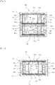
Fig. 1A is a vertical sectional view illustrating a printing step in a method for manufacturing a stack component according to an embodiment. -
Fig. 1B is a vertical sectional view illustrating a circuit element mounting step in the method for manufacturing a stack component according to the embodiment. -
Fig. 1C is a vertical sectional view illustrating an interposer mounting step in the method for manufacturing a stack component according to the embodiment. -
Fig. 1D is a vertical sectional view illustrating an interlayer connection pin inserting step in the method for manufacturing a stack component according to the embodiment. -
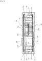
Fig. 2 is a vertical sectional view illustrating a configuration example of a stack component of vertical stacking. -
Fig. 3 is a vertical sectional view illustrating a configuration example of a stack component of face-to-face stacking. -
Fig. 4 is a vertical sectional view illustrating a configuration example of a stack component of mixed stacking. -
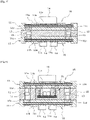
Fig. 5 is a vertical sectional view illustrating a configuration example of a stack component of stacking in a double-sided plate shape. -
Fig. 6 is a vertical sectional view illustrating a configuration example of a stack component of stacking in the double-sided plate shape with a built-in small-sized stack component. - Hereinafter, an embodiment disclosed in the present specification will be described. Each step of a method for manufacturing a stack component of the embodiment will be described with reference to
Figs. 1A to 1D . - First, as illustrated in
Fig. 1A , 3D printer (not illustrated) is used to perform a printing step of simultaneously printing and formingcircuit layer 11 and interposer 12 side by side in a planar manner onprinting stage 10 on which a print object is mounted. Interposer 12 functions as a spacer forming a space (insertion hole) for insertinginterlayer connection pin 13 betweencircuit layers 11 to be stacked. - In the printing step, at least one
circuit layer 11 amongmultiple circuit layers 11 to be stacked is simultaneously printed withinterposer 12 side by side in a planar manner, and, in a case of printingmultiple circuit layers 11,multiple circuit layers 11 are simultaneously printed and formed with interposer 12 side by side in a planar manner. In a case ofprinting interposers 12 for multiple layers, interposers 12 for multiple layers are simultaneously printed and formed withcircuit layers 11 side by side in a planar manner. - In a case where a printing space on
printing stage 10 is insufficient so that all ofmultiple circuit layers 11 andinterposers 12 to be stacked cannot be simultaneously printed side by side in a planar manner, the printing step may be divided into two or more steps. In addition, some ofcircuit layers 11 and/or some ofinterposers 12 may be formed by another forming method. - When each
circuit layer 11 is printed, insulatinglayer 11a,wiring pattern 11b,terminal section 11c, and the like are printed and formed. Insulatinglayer 11a is formed by printing insulating ink such as UV resin ink.Wiring pattern 11b andterminal section 11c are formed by printing a conductive paste, nanosilver ink, or the like. Eachinterposer 12 is formed by printing insulating ink such as UV resin ink in the same manner asinsulating layer 11a. - After the printing step is completed, the process proceeds to a circuit element mounting step, and as illustrated in
Fig. 1B ,circuit element 14 such as a semiconductor chip is mounted at a predetermined position on printedcircuit layer 11 by a mounting technique, for example, a surface mounting such as flip-chip bonding, wire bonding, or the like, and thus a terminal ofcircuit element 14 on a lower surface is connected toterminal section 11c ofcircuit layer 11. As illustrated inFigs. 4 and6 to be described later, small-sizedstack component 21 manufactured by the manufacturing method of the embodiment may be mounted at a predetermined position oncircuit layer 11. - After the circuit element mounting step is completed, the process proceeds to an interposer mounting step, as illustrated in
Fig. 1C ,interposer 12 formed onprinting stage 10 is peeled fromprinting stage 10, andinterposer 12 is mounted and bonded at a predetermined position oncircuit layer 11. - After the interposer mounting step is completed, the proceed proceeds to an interlayer connection pin inserting step, as illustrated in Fig. ID,
interlayer connection pin 13 is inserted intointerposer 12 mounted oncircuit layer 11, and a lower end ofinterlayer connection pin 13 is electrically connected toterminal section 11c ofcircuit layer 11.Interlayer connection pin 13 used in the embodiment includes a spring (not illustrated), and an upper end portion thereof is configured to be extendable and contractible by the spring. Accordingly, in a state in whichinterlayer connection pin 13 is inserted intointerposer 12, the upper end portion ofinterlayer connection pin 13 protrudes upward from an upper end ofinterposer 12. - As described above,
unit 15 of the first layer is assembled.Units 16 of the second layer and subsequent layers are assembled in the same manner. Thereafter,multiple units unit 16 on an upper layer side is stacked onunit 15 on a lower layer side, andcircuit layer 11 ofunit 16 on the upper layer side is stacked oncircuit layer 11 ofunit 15 on the lower layer side viainterposer 12, and thuscircuit layer 11 ofunit 15 on the lower layer side andcircuit layer 11 ofunit 16 on the upper layer side are electrically connected byinterlayer connection pin 13. At this time, the upper end portion ofinterlayer connection pin 13 contacts and is pushed intoterminal section 11c ofcircuit layer 11 ofunit 16 on the upper layer side, so that an electrical connection therebetween is ensured. Instead ofunit 16 on the upper layer side, onlycircuit layer 11 may be stacked. - In the manufacturing method of the embodiment, stack components having various stacking structures illustrated in
Figs. 2 to 6 can be assembled. - A stack component of vertical stacking illustrated in
Fig. 2 is a stack component in which twounits circuit layer 11 on a component surface side is stacked onunit 16 on the upper layer side.Units circuit layer 11 on the component surface side may be stacked onunit 16 of the uppermost layer. - A stack component of face-to-face stacking illustrated in
Fig. 3 is a stack component in whichunit 16 on the upper layer side among twounits unit 15 on the lower layer side in a state whereunit 16 on the upper layer side is vertically reversed. In this case, inunit 16 on the upper layer side,interposer 12 andinterlayer connection pin 13 are not mounted, onlycircuit element 14 is mounted, andcircuit layer 11 ofunit 16 on the upper layer side is stacked viainterposer 12 ofunit 15 on the lower layer side. The stack component of face-to-face stacking are in a state in whichcircuit element 14 mounted oncircuit layer 11 ofunit 16 on the upper layer side is facing downward and is accommodated inside the stack component together withcircuit element 14 mounted oncircuit layer 11 ofunit 15 on the lower layer side. - A stack component of mixed stacking illustrated in
Fig. 4 is a stack component in which small-sized stack component 21 assembled by the manufacturing method of the embodiment is mounted withcircuit element 14 side by side oncircuit layer 11 ofunit 15 on the lower layer side, andcircuit layer 11 on the component surface side is stacked onunit 15 on the lower layer side. Small-sized stack component 21 to be mounted oncircuit layer 11 ofunit 15 on the lower layer side may be assembled oncircuit layer 11 ofunit 15 on the lower layer side, or small-sized stack component 21 assembled at another location may be mounted oncircuit layer 11 ofunit 15 on the lower layer side.Circuit element 14 may be mounted on an upper surface ofcircuit layer 11 on the component surface side. In this case, since small-sized stack component 21 is mounted oncircuit layer 11 ofunit 15 on the lower layer side, multiple types ofinterposers 12 having different lengths (multiple types of interlayer connection pins 13 having different lengths) are mounted oncircuit layer 11 ofunit 15 on the lower layer side. - A stack component of stacking in a double-sided plate shape illustrated in
Fig. 5 is a stack component simulating a double-sided build-up board, in whichcircuit element 14 is mounted on a lower surface ofcircuit layer 11 ofunit 15 on the lower layer side, andcircuit element 14 is mounted on an upper surface ofcircuit layer 11 on the component surface side stacked onunit 15 on the lower layer side. In this case, inunit 16 on the upper layer side,interposer 12 andinterlayer connection pin 13 are not mounted,only circuit element 14 is mounted, andcircuit layer 11 ofunit 16 on the upper layer side is stacked viainterposer 12 ofunit 15 on the lower layer side. The step of mountingcircuit elements 14 oncircuit layers 11 of eachunit units - A stack component of stacking in the double-sided plate shape illustrated in
Fig. 6 is a stack component simulating a double-sided build-up board with a built-in component, and have a configuration in which small-sized stack component 21 is built in between layers of the stack component of stacking in the double-sided plate shape. Built-in small-sized stack component 21 may be assembled oncircuit layer 11 ofunit 15 on the lower layer side, or small-sized stack component 21 assembled at another location may be mounted oncircuit layer 11 ofunit 15 on the lower layer side. Other configurations are the same as those of the stack component of stacking in the double-sided plate shape illustrated inFig. 5 . - According to the method for manufacturing a stack component according to the embodiment described above,
circuit layer 11 andinterposer 12 are simultaneously printed and formed side by side in a planar manner on printingstage 10 by using the 3D printer,interposer 12 peeled from printingstage 10 is mounted oncircuit layer 11, and unit 15 (16) is assembled by insertinginterlayer connection pin 13 intointerposer 12. Accordingly,circuit layer 11 andinterposer 12 can be simultaneously and efficiently formed, and variations ofcircuit layer 11 andinterposer 12 can be easily diversified. In addition, since unit 15 (16) for one layer is configured by insertinginterlayer connection pin 13 intointerposer 12 mounted oncircuit layer 11, it is possible to manufacture stack components having various stacking structures illustrated inFigs. 2 to 6 , and it is also easy to diversify and increase the density of the stacking structure. - It is needless to say that the present invention is not limited to the configuration of the above embodiment, and can be implemented with various changes within the range not departing from the gist, such as changing the number of stacks of circuit layers 11 and the number of
circuit elements 14 to be mounted, or using interlayer connection pin with no built-in spring. - 10: printing stage, 11: circuit layer, 11a: insulating layer, 11b: wiring pattern, 11c: terminal section, 12: interposer, 13: interlayer connection pin, 14: circuit element, 15, 16: unit, 21: small-sized stack component
Claims (10)
- A method for manufacturing a stack component in which a circuit element is mounted on at least one circuit layer of multiple circuit layers to be stacked, the circuit layers are electrically connected by an interlayer connection pin, and an interposer is interposed to form a space for inserting the interlayer connection pin between the circuit layers, the method comprising:a printing step of simultaneously printing and forming the circuit layer and the interposer side by side in a planar manner by a 3D printer;a step of mounting the circuit element on the circuit layer;a step of mounting the interposer on the circuit layer;a step of inserting the interlayer connection pin into the interposer mounted on the circuit layer; anda step of electrically connecting the circuit layer and another circuit layer by the interlayer connection pin by stacking the other circuit layer on the circuit layer via the interposer.
- The method for manufacturing a stack component according to claim 1, wherein
in the printing step, the circuit layers of all layers constituting the stack component and the interposer are simultaneously printed and formed side by side in a planar manner. - The method for manufacturing a stack component according to claim 1, wherein
some of the circuit layers and/or some of the interposers are formed by another printing step or another forming method. - The method for manufacturing a stack component according to any one of claims 1 to 3, wherein
the interlayer connection pin is configured to be extendable and contractible by a spring. - The method for manufacturing a stack component according to any one of claims 1 to 4, wherein
as the interlayer connection pin, multiple types of interlayer connection pins having different lengths are used. - The method for manufacturing a stack component according to any one of claims 1 to 5, wherein
the circuit element and the interposer are mounted on the same surface of the circuit layer. - The method for manufacturing a stack component according to any one of claims 1 to 5, wherein
the circuit element is mounted on one surface of the circuit layer, and the interposer is mounted on the other surface. - The method for manufacturing a stack component according to any one of claims 1 to 7, further comprising:
a step of mounting a circuit element on an upper surface of an uppermost circuit layer and/or on a lower surface of a lowermost circuit layer of the stack component. - The method for manufacturing a stack component according to any one of claims 1 to 8, further comprising:a step of manufacturing a small-sized stack component by the manufacturing method according to any one of claims 1 to 7;a step of mounting the small-sized stack component and an interposer on an upper surface of a circuit layer; anda step of electrically connecting the circuit layer and another circuit layer by an interlayer connection pin by stacking the other circuit layer on the circuit layer via the small-sized stack component and the interposer.
- The method for manufacturing a stack component according to any one of claims 1 to 9, further comprising:
a step of mounting the circuit element on a lower surface of the other circuit layer before stacking the other circuit layer above the circuit layer.
Applications Claiming Priority (1)
| Application Number | Priority Date | Filing Date | Title |
|---|---|---|---|
| PCT/JP2019/029821 WO2021019684A1 (en) | 2019-07-30 | 2019-07-30 | Method for manufacturing stack components |
Publications (3)
| Publication Number | Publication Date |
|---|---|
| EP4007462A1 true EP4007462A1 (en) | 2022-06-01 |
| EP4007462A4 EP4007462A4 (en) | 2022-08-24 |
| EP4007462B1 EP4007462B1 (en) | 2026-01-14 |
Family
ID=74228358
Family Applications (1)
| Application Number | Title | Priority Date | Filing Date |
|---|---|---|---|
| EP19939888.4A Active EP4007462B1 (en) | 2019-07-30 | 2019-07-30 | Method for manufacturing stack components |
Country Status (4)
| Country | Link |
|---|---|
| US (1) | US12119327B2 (en) |
| EP (1) | EP4007462B1 (en) |
| JP (1) | JP7130875B2 (en) |
| WO (1) | WO2021019684A1 (en) |
Families Citing this family (2)
| Publication number | Priority date | Publication date | Assignee | Title |
|---|---|---|---|---|
| WO2022244392A1 (en) | 2021-05-18 | 2022-11-24 | 富士電機株式会社 | Semiconductor device and production method for semiconductor device |
| JPWO2024018615A1 (en) * | 2022-07-22 | 2024-01-25 |
Family Cites Families (7)
| Publication number | Priority date | Publication date | Assignee | Title |
|---|---|---|---|---|
| JPH07193350A (en) * | 1993-12-27 | 1995-07-28 | Kokusai Electric Co Ltd | High frequency signal connection device |
| JP2001352176A (en) | 2000-06-05 | 2001-12-21 | Fuji Xerox Co Ltd | Multilayer printed wiring board and method for manufacturing multilayer printed wiring board |
| JP4888073B2 (en) | 2006-11-16 | 2012-02-29 | セイコーエプソン株式会社 | Manufacturing method of electronic substrate |
| WO2008136251A1 (en) * | 2007-05-02 | 2008-11-13 | Murata Manufacturing Co., Ltd. | Component-incorporating module and its manufacturing method |
| JP2017130553A (en) * | 2016-01-20 | 2017-07-27 | 株式会社ミマキエンジニアリング | Method for manufacturing electronic element installation base material, method for manufacturing electronic component, and molding device |
| CN109314086B (en) | 2016-06-08 | 2022-11-04 | 株式会社富士 | circuit formation method |
| WO2019102522A1 (en) * | 2017-11-21 | 2019-05-31 | 株式会社Fuji | Three-dimensional multi-layer electronic device production method and three-dimensional multi-layer electronic device |
-
2019
- 2019-07-30 US US17/630,870 patent/US12119327B2/en active Active
- 2019-07-30 WO PCT/JP2019/029821 patent/WO2021019684A1/en not_active Ceased
- 2019-07-30 EP EP19939888.4A patent/EP4007462B1/en active Active
- 2019-07-30 JP JP2021536514A patent/JP7130875B2/en active Active
Also Published As
| Publication number | Publication date |
|---|---|
| US20220271010A1 (en) | 2022-08-25 |
| EP4007462A4 (en) | 2022-08-24 |
| JPWO2021019684A1 (en) | 2021-02-04 |
| US12119327B2 (en) | 2024-10-15 |
| JP7130875B2 (en) | 2022-09-05 |
| EP4007462B1 (en) | 2026-01-14 |
| WO2021019684A1 (en) | 2021-02-04 |
Similar Documents
| Publication | Publication Date | Title |
|---|---|---|
| KR101084252B1 (en) | Electronic printed circuit board and its manufacturing method | |
| JP6129415B2 (en) | Detachable electrical connection structure and electrical connection connector, semiconductor package assembly, and electronic device equipped with the same | |
| US8963013B2 (en) | Three dimensional interposer device | |
| US20120018193A1 (en) | Multi layer circuit board and method of manufacturing the same | |
| KR20100106938A (en) | Connector having a lock mechanism for keeping a socket and a header coupled, and method for manufacturing the connector | |
| KR101689547B1 (en) | Method for manufacturing electrical interconnection structure | |
| US20100097770A1 (en) | Printed circuit board and manufacturing method thereof | |
| CN108353500B (en) | Substrate device and method for manufacturing substrate device | |
| US20160270222A1 (en) | Multilayer wiring board and probe card having the same | |
| EP4007462B1 (en) | Method for manufacturing stack components | |
| US20130058032A1 (en) | Portable data storage devices and hosts compliant with multiple communications standards | |
| US20180013219A1 (en) | Matable electrical interconnection structure and electrical device having the same | |
| EP2849226B1 (en) | Semiconductor package | |
| CN100492680C (en) | Multi-layer surface mount light emitting diode | |
| JP4033157B2 (en) | Conducting path forming method | |
| CN101257767A (en) | Printed circuit board and manufacturing method thereof | |
| JP2010114074A (en) | Connector for inserting substrate, and its manufacturing method | |
| US20150380347A1 (en) | Semiconductor device and method of manufacturing semiconductor device | |
| CN214542186U (en) | Packaged chips and mobile terminals | |
| US8304895B2 (en) | Semiconductor package and method of fabricating the same | |
| JP2012109386A (en) | Wiring board | |
| JP4746376B2 (en) | Ceramic multilayer substrate and manufacturing method thereof | |
| JP3189807U (en) | Connector and connector device | |
| KR101251660B1 (en) | Printed circuit board, pcb card using the printed circuit board, method for manufacturing the printed circuit board and the pcb card | |
| JP2001053217A (en) | Stack carrier for three-dimensional semiconductor device and three-dimensional semiconductor device |
Legal Events
| Date | Code | Title | Description |
|---|---|---|---|
| STAA | Information on the status of an ep patent application or granted ep patent |
Free format text: STATUS: THE INTERNATIONAL PUBLICATION HAS BEEN MADE |
|
| PUAI | Public reference made under article 153(3) epc to a published international application that has entered the european phase |
Free format text: ORIGINAL CODE: 0009012 |
|
| STAA | Information on the status of an ep patent application or granted ep patent |
Free format text: STATUS: REQUEST FOR EXAMINATION WAS MADE |
|
| 17P | Request for examination filed |
Effective date: 20220105 |
|
| AK | Designated contracting states |
Kind code of ref document: A1 Designated state(s): AL AT BE BG CH CY CZ DE DK EE ES FI FR GB GR HR HU IE IS IT LI LT LU LV MC MK MT NL NO PL PT RO RS SE SI SK SM TR |
|
| A4 | Supplementary search report drawn up and despatched |
Effective date: 20220725 |
|
| RIC1 | Information provided on ipc code assigned before grant |
Ipc: B33Y 80/00 20150101ALN20220719BHEP Ipc: B33Y 10/00 20150101ALN20220719BHEP Ipc: H05K 1/14 20060101ALI20220719BHEP Ipc: H05K 3/46 20060101AFI20220719BHEP |
|
| DAV | Request for validation of the european patent (deleted) | ||
| DAX | Request for extension of the european patent (deleted) | ||
| P01 | Opt-out of the competence of the unified patent court (upc) registered |
Effective date: 20230328 |
|
| GRAP | Despatch of communication of intention to grant a patent |
Free format text: ORIGINAL CODE: EPIDOSNIGR1 |
|
| STAA | Information on the status of an ep patent application or granted ep patent |
Free format text: STATUS: GRANT OF PATENT IS INTENDED |
|
| RIC1 | Information provided on ipc code assigned before grant |
Ipc: H05K 3/46 20060101AFI20250903BHEP Ipc: H05K 1/14 20060101ALI20250903BHEP Ipc: B33Y 10/00 20150101ALN20250903BHEP Ipc: B33Y 80/00 20150101ALN20250903BHEP |
|
| INTG | Intention to grant announced |
Effective date: 20250917 |
|
| GRAS | Grant fee paid |
Free format text: ORIGINAL CODE: EPIDOSNIGR3 |
|
| GRAA | (expected) grant |
Free format text: ORIGINAL CODE: 0009210 |
|
| STAA | Information on the status of an ep patent application or granted ep patent |
Free format text: STATUS: THE PATENT HAS BEEN GRANTED |
|
| AK | Designated contracting states |
Kind code of ref document: B1 Designated state(s): AL AT BE BG CH CY CZ DE DK EE ES FI FR GB GR HR HU IE IS IT LI LT LU LV MC MK MT NL NO PL PT RO RS SE SI SK SM TR |
|
| REG | Reference to a national code |
Ref country code: CH Ref legal event code: F10 Free format text: ST27 STATUS EVENT CODE: U-0-0-F10-F00 (AS PROVIDED BY THE NATIONAL OFFICE) Effective date: 20260114 Ref country code: GB Ref legal event code: FG4D |
|
| REG | Reference to a national code |
Ref country code: DE Ref legal event code: R096 Ref document number: 602019080487 Country of ref document: DE |
|
| REG | Reference to a national code |
Ref country code: IE Ref legal event code: FG4D |
|
| REG | Reference to a national code |
Ref country code: NL Ref legal event code: MP Effective date: 20260114 |
|
| PG25 | Lapsed in a contracting state [announced via postgrant information from national office to epo] |
Ref country code: NL Free format text: LAPSE BECAUSE OF FAILURE TO SUBMIT A TRANSLATION OF THE DESCRIPTION OR TO PAY THE FEE WITHIN THE PRESCRIBED TIME-LIMIT Effective date: 20260114 |
|
| REG | Reference to a national code |
Ref country code: AT Ref legal event code: MK05 Ref document number: 1877962 Country of ref document: AT Kind code of ref document: T Effective date: 20260114 |
|
| PG25 | Lapsed in a contracting state [announced via postgrant information from national office to epo] |
Ref country code: RS Free format text: LAPSE BECAUSE OF FAILURE TO SUBMIT A TRANSLATION OF THE DESCRIPTION OR TO PAY THE FEE WITHIN THE PRESCRIBED TIME-LIMIT Effective date: 20260414 |
|
| PG25 | Lapsed in a contracting state [announced via postgrant information from national office to epo] |
Ref country code: ES Free format text: LAPSE BECAUSE OF FAILURE TO SUBMIT A TRANSLATION OF THE DESCRIPTION OR TO PAY THE FEE WITHIN THE PRESCRIBED TIME-LIMIT Effective date: 20260114 |
|
| PG25 | Lapsed in a contracting state [announced via postgrant information from national office to epo] |
Ref country code: PL Free format text: LAPSE BECAUSE OF FAILURE TO SUBMIT A TRANSLATION OF THE DESCRIPTION OR TO PAY THE FEE WITHIN THE PRESCRIBED TIME-LIMIT Effective date: 20260114 |
|
| PG25 | Lapsed in a contracting state [announced via postgrant information from national office to epo] |
Ref country code: GR Free format text: LAPSE BECAUSE OF FAILURE TO SUBMIT A TRANSLATION OF THE DESCRIPTION OR TO PAY THE FEE WITHIN THE PRESCRIBED TIME-LIMIT Effective date: 20260415 |
|
| REG | Reference to a national code |
Ref country code: LT Ref legal event code: MG9D |
|
| PG25 | Lapsed in a contracting state [announced via postgrant information from national office to epo] |
Ref country code: LT Free format text: LAPSE BECAUSE OF FAILURE TO SUBMIT A TRANSLATION OF THE DESCRIPTION OR TO PAY THE FEE WITHIN THE PRESCRIBED TIME-LIMIT Effective date: 20260114 |
|
| PG25 | Lapsed in a contracting state [announced via postgrant information from national office to epo] |
Ref country code: NO Free format text: LAPSE BECAUSE OF FAILURE TO SUBMIT A TRANSLATION OF THE DESCRIPTION OR TO PAY THE FEE WITHIN THE PRESCRIBED TIME-LIMIT Effective date: 20260414 |
|
| PG25 | Lapsed in a contracting state [announced via postgrant information from national office to epo] |
Ref country code: SE Free format text: LAPSE BECAUSE OF FAILURE TO SUBMIT A TRANSLATION OF THE DESCRIPTION OR TO PAY THE FEE WITHIN THE PRESCRIBED TIME-LIMIT Effective date: 20260114 Ref country code: FI Free format text: LAPSE BECAUSE OF FAILURE TO SUBMIT A TRANSLATION OF THE DESCRIPTION OR TO PAY THE FEE WITHIN THE PRESCRIBED TIME-LIMIT Effective date: 20260114 Ref country code: AT Free format text: LAPSE BECAUSE OF FAILURE TO SUBMIT A TRANSLATION OF THE DESCRIPTION OR TO PAY THE FEE WITHIN THE PRESCRIBED TIME-LIMIT Effective date: 20260114 |
|
| PG25 | Lapsed in a contracting state [announced via postgrant information from national office to epo] |
Ref country code: HR Free format text: LAPSE BECAUSE OF FAILURE TO SUBMIT A TRANSLATION OF THE DESCRIPTION OR TO PAY THE FEE WITHIN THE PRESCRIBED TIME-LIMIT Effective date: 20260114 |
|
| PG25 | Lapsed in a contracting state [announced via postgrant information from national office to epo] |
Ref country code: PT Free format text: LAPSE BECAUSE OF FAILURE TO SUBMIT A TRANSLATION OF THE DESCRIPTION OR TO PAY THE FEE WITHIN THE PRESCRIBED TIME-LIMIT Effective date: 20260514 Ref country code: IS Free format text: LAPSE BECAUSE OF FAILURE TO SUBMIT A TRANSLATION OF THE DESCRIPTION OR TO PAY THE FEE WITHIN THE PRESCRIBED TIME-LIMIT Effective date: 20260514 |
|
| PG25 | Lapsed in a contracting state [announced via postgrant information from national office to epo] |
Ref country code: LV Free format text: LAPSE BECAUSE OF FAILURE TO SUBMIT A TRANSLATION OF THE DESCRIPTION OR TO PAY THE FEE WITHIN THE PRESCRIBED TIME-LIMIT Effective date: 20260114 |
|
| PG25 | Lapsed in a contracting state [announced via postgrant information from national office to epo] |
Ref country code: BG Free format text: LAPSE BECAUSE OF FAILURE TO SUBMIT A TRANSLATION OF THE DESCRIPTION OR TO PAY THE FEE WITHIN THE PRESCRIBED TIME-LIMIT Effective date: 20260114 |