EP4007298A1 - Digital microphone with low data rate interface - Google Patents
Digital microphone with low data rate interface Download PDFInfo
- Publication number
- EP4007298A1 EP4007298A1 EP21210212.3A EP21210212A EP4007298A1 EP 4007298 A1 EP4007298 A1 EP 4007298A1 EP 21210212 A EP21210212 A EP 21210212A EP 4007298 A1 EP4007298 A1 EP 4007298A1
- Authority
- EP
- European Patent Office
- Prior art keywords
- data rate
- low data
- mems
- feature extraction
- features
- Prior art date
- Legal status (The legal status is an assumption and is not a legal conclusion. Google has not performed a legal analysis and makes no representation as to the accuracy of the status listed.)
- Pending
Links
Images





Classifications
-
- H—ELECTRICITY
- H04—ELECTRIC COMMUNICATION TECHNIQUE
- H04R—LOUDSPEAKERS, MICROPHONES, GRAMOPHONE PICK-UPS OR LIKE ACOUSTIC ELECTROMECHANICAL TRANSDUCERS; ELECTRIC HEARING AIDS; PUBLIC ADDRESS SYSTEMS
- H04R1/00—Details of transducers, loudspeakers or microphones
- H04R1/08—Mouthpieces; Microphones; Attachments therefor
- H04R1/083—Special constructions of mouthpieces
-
- H—ELECTRICITY
- H04—ELECTRIC COMMUNICATION TECHNIQUE
- H04R—LOUDSPEAKERS, MICROPHONES, GRAMOPHONE PICK-UPS OR LIKE ACOUSTIC ELECTROMECHANICAL TRANSDUCERS; ELECTRIC HEARING AIDS; PUBLIC ADDRESS SYSTEMS
- H04R19/00—Electrostatic transducers
- H04R19/005—Electrostatic transducers using semiconductor materials
-
- B—PERFORMING OPERATIONS; TRANSPORTING
- B81—MICROSTRUCTURAL TECHNOLOGY
- B81B—MICROSTRUCTURAL DEVICES OR SYSTEMS, e.g. MICROMECHANICAL DEVICES
- B81B3/00—Devices comprising flexible or deformable elements, e.g. comprising elastic tongues or membranes
- B81B3/0018—Structures acting upon the moving or flexible element for transforming energy into mechanical movement or vice versa, i.e. actuators, sensors, generators
- B81B3/0021—Transducers for transforming electrical into mechanical energy or vice versa
-
- H—ELECTRICITY
- H04—ELECTRIC COMMUNICATION TECHNIQUE
- H04R—LOUDSPEAKERS, MICROPHONES, GRAMOPHONE PICK-UPS OR LIKE ACOUSTIC ELECTROMECHANICAL TRANSDUCERS; ELECTRIC HEARING AIDS; PUBLIC ADDRESS SYSTEMS
- H04R1/00—Details of transducers, loudspeakers or microphones
- H04R1/02—Casings; Cabinets ; Supports therefor; Mountings therein
-
- H—ELECTRICITY
- H04—ELECTRIC COMMUNICATION TECHNIQUE
- H04R—LOUDSPEAKERS, MICROPHONES, GRAMOPHONE PICK-UPS OR LIKE ACOUSTIC ELECTROMECHANICAL TRANSDUCERS; ELECTRIC HEARING AIDS; PUBLIC ADDRESS SYSTEMS
- H04R1/00—Details of transducers, loudspeakers or microphones
- H04R1/02—Casings; Cabinets ; Supports therefor; Mountings therein
- H04R1/04—Structural association of microphone with electric circuitry therefor
-
- H—ELECTRICITY
- H04—ELECTRIC COMMUNICATION TECHNIQUE
- H04R—LOUDSPEAKERS, MICROPHONES, GRAMOPHONE PICK-UPS OR LIKE ACOUSTIC ELECTROMECHANICAL TRANSDUCERS; ELECTRIC HEARING AIDS; PUBLIC ADDRESS SYSTEMS
- H04R19/00—Electrostatic transducers
- H04R19/04—Microphones
-
- B—PERFORMING OPERATIONS; TRANSPORTING
- B81—MICROSTRUCTURAL TECHNOLOGY
- B81B—MICROSTRUCTURAL DEVICES OR SYSTEMS, e.g. MICROMECHANICAL DEVICES
- B81B2201/00—Specific applications of microelectromechanical systems
- B81B2201/02—Sensors
- B81B2201/0257—Microphones or microspeakers
-
- H—ELECTRICITY
- H04—ELECTRIC COMMUNICATION TECHNIQUE
- H04R—LOUDSPEAKERS, MICROPHONES, GRAMOPHONE PICK-UPS OR LIKE ACOUSTIC ELECTROMECHANICAL TRANSDUCERS; ELECTRIC HEARING AIDS; PUBLIC ADDRESS SYSTEMS
- H04R2201/00—Details of transducers, loudspeakers or microphones covered by H04R1/00 but not provided for in any of its subgroups
- H04R2201/003—Mems transducers or their use
Definitions
- the present invention relates generally to a digital microphone with a low data rate interface and to a corresponding method.
- Digital microphones are used convert audio input signals into corresponding digital output signals.
- Typical digital microphones include high data rate interfaces including digital signal processing circuitry in order to convert the audio input signals into high quality digital output signals. Due to the always-on nature of the digital microphone and the high power consumption of the digital circuits in the high data rate interface, the use of the digital microphone in portable devices with battery life limitations can be strongly restricted. Manufacturers and customers desire digital microphones with a low data rate interface in order to reduce power and to extend battery life without a significant loss of performance.
- a MEMS system includes a MEMS device; a feature extraction component coupled to an output of the MEMS device, wherein the feature extraction component is configured to provide a plurality of features of an output signal of the MEMS device; and a low data rate interface coupled to the feature extraction components, wherein the low data rate interface is configured to transmit the plurality of features of the output signal of the MEMS device, and wherein a low data rate of the low data rate interface is determined by a number of the plurality of features transmitted, wherein the MEMS device, the feature extraction component, and the low data rate interface are packaged together in a semiconductor package.
- a conversion method includes converting an environmental change into an output signal using a MEMS device; extracting a plurality of features from the output signal of the MEMS device; and transmitting the plurality of features through a low data rate interface, wherein a low data rate of the low data rate interface is determined by a number of the plurality of features transmitted, and wherein the conversion method is practiced by one or more integrated circuits in a single semiconductor package.
- a MEMS system includes a MEMS microphone; a feature extraction component coupled to an output of the MEMS microphone, wherein the feature extraction component is configured to provide a plurality of features of an output signal of the MEMS microphone; a low data rate interface coupled to the feature extraction component, wherein the low data rate interface is configured to transmit the plurality of features of the output signal of the MEMS device, and wherein a low data rate of the low data rate interface is determined by a number of the plurality of features transmitted; and a codec coupled to the low data rate interface for digitally processing the plurality of transmitted features, wherein the MEMS microphone, the feature extraction component, and the low data rate interface are integrated together on one or more integrated circuits in a single semiconductor package.
- a digital microphone system comprises a MEMS device and an Application Specific Integrated Circuit (ASIC) including a feature extraction component and a low data rate interface coupled to the MEMS device.
- the feature extraction component extracts a plurality of features that highlight the most dominating and discriminating characteristics from the analog output signal of the MEMS devices.
- a high quality replica of the analog digital output can be constructed solely from the plurality of features if desired.
- the detected features can be used in conjunction with voice recognition applications to initiate or perform various functions.
- the feature extraction of the feature extraction component can be conducted in the analog or digital domain.
- the ASIC is coupled to an external audio coder-decoder (codec) that may include one or more applications that include voice activity detection (VAD), keyword detection (KWD), and voice recognition applications.
- codec an external audio coder-decoder
- VAD voice activity detection
- WCD keyword detection
- voice recognition applications voice recognition applications
- VAD voice activity detection
- WCD keyword detection
- voice recognition applications voice recognition applications
- VAD voice activity detection
- WCD keyword detection
- the feature extraction is conducted in the analog domain.
- an analog-to-digital converter is used to convert the analog features into digital features for subsequent digital signal processing in the digital microphone system.
- the power required to perform the analog-to-digital conversion of the analog features is much lower than the power required to perform a full analog-to-digital conversion of an analog audio signal.
- the power can be significantly reduced because the clock rate of the analog-to-digital converter can also be significantly reduced.
- the digital microphone system according to embodiments can be used in many extremely low power applications.
- the power requirements of the digital microphone system can be advantageously reduced to less than forty microwatts, preferably less than thirty microwatts, preferably less than twenty microwatts, and preferably less than ten microwatts.
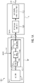
- FIG. 1A is a block diagram of an exemplary system partitioning of a digital microphone system 100A, particularly configured for standard voice recognition applications.
- the digital microphone system 100A includes a digital microphone 102 comprising a MEMS component 104 coupled to an input of ASIC 107 through the analog output 106 of the MEMS component 104.
- the MEMS component 104 can comprise a MEMS microphone component.
- ASIC 107 includes an analog-to-digital converter (ADC) 108 for converting the analog signal at the analog output 106 into a digital code.
- the digital code is typically filtered by a digital filter 110 coupled to the output of ADC 108.
- ASIC 107 typically includes a digital modulator into a single bit digital stream at the digital microphone output 116.
- ASIC 107 receives a clock signal at clock input 114 to distribute to one or more of the ASIC components including ADC 108, digital filter 110, and/or digital modulator 112.
- Microphone system 100A typically includes an audio codec 118 including keyword detection, voice activity detection, or voice recognition applications.
- a codec output 124 provides a digital signal with output data generated by the keyword detection, voice activity detection, or voice recognition application.
- the MEMS microphone 104 senses acoustic signals and the ASIC 107 transmits a single bit signal to a processor (not shown in Figure 1 ).
- the single bit signal can be encoded using Pulse Code Modulation (PCM) or Pulse Density Modulation (PDM).
- PCM Pulse Code Modulation
- PDM Pulse Density Modulation
- DSP component 120 Further digital signal processing functionality is performed such as feature extraction in DSP component 120, and the voice activity detection (VAD), keyword detection (KWD) or voice recognition is performed in voice recognition component 122.
- DSP block 120 has an input coupled to the digital microphone output 116, and voice recognition component 122 has an output coupled to codec output 124.
- a standard digital microphone typically provides a single bit stream at a low data rate (for example 768 kHz in a low power operational mode) or at a high data rate (for example 2.4 to 3 MHz in high performance operational mode).
- the high performance operational mode leads to high power dissipation in ASIC 107 due to the high clock rate required by ADC 108.
- FIG 1B is a graph of CMOS interface power versus frequency for the digital microphone 102 and audio codec 118 of Figure 1A , wherein "interface power" can be defined as the power required by digital microphone 102 to provide the single bit digital stream at digital microphone output 116, which is the interface to further processing circuitry such as audio codec 118.
- interface power can be defined as the power required by digital microphone 102 to provide the single bit digital stream at digital microphone output 116, which is the interface to further processing circuitry such as audio codec 118.
- a 50 pF load capacitance is assumed at digital microphone output 116.
- a power consumption as low as 200 ⁇ W is achieved but further power reduction is required for some battery powered applications.
- the power dissipation of a CMOS interface is depicted versus activity of the interface for two interface voltages.
- a first line 126 represents interface power versus clock frequency at an interface power supply voltage of 1.8 volts.
- a second line 128 represents interface power versus clock frequency at an interface power supply voltage of 1.2 volts.
- a reasonably-sized load capacitance of 50 pf is assumed. At higher clock frequencies, with a load capacitor of 50 pf, the power needed for data communication is significant compared to the digital microphone power.
- Both the clock line 114 and the data line at digital microphone output 116 define the high power requirements at higher frequencies. At a 768 kHz clock rate, for example, interface power requirements are 120 ⁇ W (at 1.8 volts) or 56 ⁇ W (at 1.2 volts).
- What is desired is to reduce the interface data rate and the clock rate significantly, such that the power consumption for the interface can be reduced to single digit ⁇ W numbers, which is less than 10 microwatts.
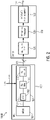
- FIG. 2 is a block diagram of an exemplary system partitioning of a digital microphone system 100B including digital microphone and audio codec 118.
- Digital microphone system 100B is similar to previously described digital microphone system 100A, except that audio codec 118 includes a decimation filter 126.
- audio codec 118 includes a decimation filter 126.
- decimation filter 126 implements a method of observing only a periodic portion of the ADC samples, while ignoring the rest. The result is to reduce the sample rate of ADC 108. For example, a decimate-by-4 mode would mean that the total samples passing through the decimation filter 126 are reduced by a factor of four, while all of the other samples are effectively discarded.
- Digital filtering using decimation filter 126 effectively removes the out-of-band noise from the narrowly defined bandwidth that is set by the decimation ratio.
- An additional aspect of the digital microphone system configuration shown in Figure 2 is that for the feature extraction the audio signal with full quality is not needed, which leads to additional overhead in the digital microphone (for example the high quality ADC 108) and also in subsequent digital signal processing (for example the decimation filter 126). The additional overhead may also increase the power requirements of digital microphone system 100B in high clock rate (high performance) applications.
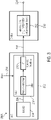
- FIG 3 is a block diagram of a digital microphone system 200A comprising a digital microphone 202 with a low data rate interface and an audio codec 218 according to an embodiment.
- Digital microphone 202 includes a MEMS component such as a MEMS microphone 204, which has an analog output 206.
- the MEMS microphone 204 is coupled to ASIC 207.
- ASIC 207 comprises a feature extraction component 208, which is configured to extract audio features in the analog or digital domain.
- the feature extraction component 208 shown in Figure 4 can include analog, digital, or combined solutions to provide the feature extraction functionality. Specific embodiments of the feature extraction component 208 are described below.
- a low data rate interface component 210 is coupled between the feature extraction component 208 and the output 216 of the digital microphone 202.
- Digital microphone 202 includes a clock input 214 for receiving a clock signal from a processor (not shown in Figure 3 ). The clock signal is then distributed to the feature extraction component 208 and/or the low data rate interface 210.
- the digital microphone system 200A includes an audio codec 218 coupled to the output 216 of digital microphone 202. Audio codec 218 is configured with one or more applications, such as a voice activity detection (VAD), keyword detection (KWD) or voice recognition and generates a corresponding digital signal at codec output 224. Audio codec 218 is described in further detail below.
- VAD Voice Activity Detection
- voice activity detection is sometimes also referred to as a “wake-on-voice” process or a “wake-on-speech” process.
- Key Word Spotting or “Keyword Detection” (KWD) may refer to a process that detects a specific spoken word or phrase.
- key word spotting is also sometimes referred to as a voice trigger.
- the typical design of a VAD algorithm may include: an initial noise reduction stage, e.g.
- spectral subtraction via spectral subtraction; a calculation of features or quantities from a section of the input signal; and the application of a classification rule to classify the section as speech or non-speech, wherein the classification rule is invoked when a value of the calculated feature or quantity exceeds a predetermined threshold.
- Voice recognition can be used to identify a specific speaker, for example in security applications.
- Numerous voice recognition algorithms can be used including using Hidden Markov models, dynamic time warping (DTW)-based speech recognition, training neural networks, and "end-to-end” automatic speech recognition techniques using simplified voice models that can be used at low audio frame rates.
- DTW dynamic time warping
- digital microphone 202 comprises one or more integrated circuits in a semiconductor package.
- the semiconductor package comprises a metal, plastic, glass, or ceramic casing comprising one or more discrete semiconductor devices or integrated circuits. Any suitable type of semiconductor package can be used.
- MEMS microphone 204 comprises a first integrated circuit and ASIC 207 comprises a second integrated circuit coupled to the first integrated circuit.
- a single integrated circuit comprises a common substrate including MEMS microphone 204 and ASIC 207.
- audio codec 218 is external to digital microphone 202.
- digital microphone system 200A shown in Figure 3 advantageously minimizes the additional overhead of the signal processing components shown and described with respect to the exemplary digital microphone system 100A of Figure 1A , and the exemplary digital microphone system 100B of Figure 1B , and significantly reduces the associated power consumption.
- the data at the output 216 of low data interface 210 are encoded with the extracted features of the voice/audio signal detected by MEMS microphone 203, whereas in the exemplary digital microphone systems described above the full digital time domain voice/audio signal is applied to the interface.
- all or part of the feature extraction functionality is located in the digital microphone 202 and the features are transmitted to subsequent processing circuitry. By transmitting only the detected features, the data rate at the interface can be reduced significantly leading to reduced power consumption. Data rates for various encoding techniques are described below with respect the table of Figure 9 .
- Figure 4 illustrates an embodiment digital microphone 200B in which feature extraction is performed in the analog domain, and thus an additional analog-to-digital converter 220 is interposed between the feature extraction component 208 and the low data rate interface 210.
- decimation filter 126 and feature extraction component 120 previously shown in Figure 2 may now be removed from the digital signal processing chain, according to embodiments, reducing product costs and reducing power requirements.
- FIG. 5A is a schematic diagram of a feature extraction component including a biquad filter 500, according to an embodiment.
- the feature extraction component of Figure 5A is suitable for use as the extraction component previously described above.
- the biquad filter 500 includes a first integrator 508 coupled to a second integrator 510.
- the integrators 508 and 510 both have a transfer function of ⁇ o /S, wherein " ⁇ o " is related to the corner frequency of the integrator and "S" is the integrating transfer function in the frequency domain.
- the input of the biquad filter 500 x(t) is coupled to an input 502 of a summer 506.
- the output of summer 506 is coupled to the input of integrator 508.
- the output of integrator 508 is coupled to the output node 504 of the biquad filter, y(t).
- the input of integrator 510 is coupled to output node 504, and the output of integrator 510 is coupled to a negative input of summer 506.
- the output node 504 of the biquad filter is coupled to another negative input of summer 506 through an amplifier 512.
- the gain of the amplifier is set to 1/Q, wherein "Q" is the quality factor of the biquad filter.
- Biquad filter 500 can be implemented in the analog or digital domain. If implemented in the analog domain, a digital-to-analog conversion is required for converting the analog output of biquad filter 500. However, the ADC used for the conversion can be operated with a relatively low sample rate.
- the corner frequency of the integrators 508 and 510, and the gain of amplifier 512 can be adjusted as desired to extract the essential features from the analog signal present at the input node 502.
- the biquad filter 500 shown in Figure 5A can be implemented using, for example, one or more voltage-controlled oscillators (VCOs) as will be described in further detail below, particularly with respect to Figure 6 .
- VCOs produce similar signals obtained from an analog filter, but encoded in the frequency of a square wave instead of in an analog voltage or analog current.
- the output signal y(t) provided by the filter is differential, i.e. there is a square wave for the positive signal and another square wave for the negative signal. These square waves are generated in the internal VCOs of the filters as is described in further detail below.
- an averaging circuit is used. This averaging circuit may comprise a counter counting up with the positive signal and counting down with the negative signal. The absolute value of this counter taken periodically represents the average power of the output of the filter and this can be used as the feature value.
- An averaging circuit is described below with respect to Figure 5B .
- An averaging circuit including, for example a counter and an absolute value circuit, is used to average the filtered signal at node 504, y(t), to produce the useful information for extracting the feature values.
- a schematic diagram of an averaging circuit 520 is shown in Figure 5B having a counter 522 coupled to input node 502, which is the differential output nodes 504P and 504N of biquad filter 500 shown in Figure 5A .
- the positive output signal node 504P is coupled to the "UP" counter input of counter 522, and the negative output signal node 504N is coupled to the "DOWN" counter input of counter 522.
- the counter 522 is coupled to a first register 524.
- Register 524 also receives a clock signal at node 526 whose frequency rate determines the update rate of the feature extraction.
- Register 524 is coupled to an absolute value circuit 530.
- the absolute value may be calculated by simply stripping the sign bit of the output of register 524; other methods of determining an absolute value, however, may also be used.
- other non-linear functions can be applied instead of an absolute value function, such as a squaring function.
- the absolute value circuit is coupled to an additional integrator circuit 532.
- Integrator circuit 532 can be implemented as an accumulator circuit including an arithmetic logic unit (ALU) having a first input coupled to the absolute value circuit 530, and a second input coupled to an output of the ALU.
- ALU arithmetic logic unit
- the integrator circuit is coupled to a second register 534.
- the output of register 534 is coupled to output node 528, which provides the output feature values.
- Register 534 also receives a clock signal at node 536 whose frequency rate periodically updates the output feature value at node 528.
- any suitable counters can be used for counter 522 and any suitable registers can be used for register 524 and for register 534.
- Other types of arrangements of the components shown in averaging circuit 520 may be used, and other types of averaging circuits may also be used.
- the feature extraction algorithm can be based on autocorrelation coefficients.
- Another approach is based on a band pass filter bank, implemented with a voltage-controlled oscillator (VCO). VCO and autocorrelation coefficient feature extraction embodiments are described below with respect to Figure 6 and Figure 7 .
- FIG 6 is a schematic diagram of a feature extraction component 600 including a voltage-controlled oscillator and a counter, according an embodiment.
- the VCO-based feature extraction component 600 is similar in configuration to the biquad filter 500 shown in Figure 5 .
- each of the integrators are implemented with a VCO and counter configuration that is described in further detail below.
- the feature extraction component 600 includes a summer having a positive input coupled to input node 602 for receiving an analog input signal x(t).
- the output of summer 608 is coupled to a first integrator 612A.
- the output of first integrator 612A is coupled to an amplifier 618A having a gain "G".
- the output of amplifier 618A is coupled to output node 604 for providing a digital output, y(t).
- a second integrator 612B has an input coupled to output node 604 and an output coupled to an input of amplifier 618B having a gain "G".
- the output of amplifier 618B is coupled to a negative input of summer 608.
- the digital output signal y(t) is fed back to another negative input of summer 608 through amplifier 610 having a gain of 1/Q, wherein "Q" is the quality factor of the VCO-based feature extraction component 600.
- the digital output signal y(t) at output node 604 is coupled to the input of an averaging circuit 630, which provides the output feature values at node 632.
- Averaging circuit 630 can be similar to averaging circuit 520 shown in Figure 5B in an embodiment. However, any suitable averaging circuits can also be used.
- the corner frequency of the integrators 612A and 612B, and the gain of amplifiers 618A, 618B, and 610 can be adjusted as desired to extract the essential features from the analog signal present at the input node 602.
- the first integrator 612A includes a first VCO 614A having an output coupled to an "up" counter input of counter 616A designated C 1 .
- a “down” counter input of counter 616A receives a clock signal 606 designated “f o ".
- the output of counter 616A is coupled to the input of amplifier 618A.
- the second integrator 612B includes a second VCO 614B having an output coupled to an "up” counter input of counter 616B designated C2.
- a “down” counter input of counter 616A receives the clock signal 606 designated "f o ".
- the output of counter 616B is coupled to the input of amplifier 618B.
- the VCO implementation shown in Figure 6 has an advantage of not requiring an analog to digital conversion prior to the filter bank, which operates on the frequency encoded signal (from the VCO).
- the VCO-based filters behave similar to analog band pass filters but their operation uses digital, frequency encoded signals that are processed by VCO oscillators and digital primitives.
- Voice band energy is estimated in the digital domain without requiring an explicit analog-to-digital converter for power estimation, as the signal energy can be measured by counting pulses at the filter output.
- the ADC 220 shown in Figure 4 is thus not required in the VCO implementation shown in Figure 6 .
- the mostly digital nature of the VCO implementation shown in Figure 6 allows the use of a subnanometer semiconductor fabrication technology for all of the digital microphone system electronics.
- the digital microphone 202 and the audio codec 218 shown in Figure 3 and Figure 4 can be integrated together on a single subnanometer integrated circuit having a common substrate.
- digital microphone 202 can be integrated on a first integrated circuit
- audio codec 218 can be integrated on a second integrated circuit coupled to the first integrated circuit.
- FIG. 7 is a block diagram of a feature extraction component 700 comprising an auto-correlation component, according to an embodiment.
- the autocorrelation algorithm is a measure of the similarities of the analog or digital signal with a replica copy containing a time lag.
- the autocorrelation based feature extraction comprises an autocorrelation function in combination with a Fast Fourier Transformation (FFT) function.
- FFT Fast Fourier Transformation
- the feature extraction component 700 (without the FFT function) can be implemented in its entirety inside of the digital microphone.
- a part of the autocorrelation feature extraction component 700 could also be implemented in the audio codec, e.g. the calculation of the autocorrelation coefficients in the digital microphone as well as the FFT function.
- the feature extraction component 700 includes an input node 702 for receiving an analog input signal 702.
- a multiplier 712 includes a first input for receiving the input signal 702, x(t).
- the multiplier 712 includes a second input 708 for receiving a time-delayed replica of the input signal, x(t- ⁇ ), wherein ⁇ is the delay value.
- the output of multiplier 712 generates the product of the two input signals, which is equal to x(t) ⁇ x(t- ⁇ ).
- the output signal of multiplier 712 is averaged over a time interval T by averaging circuit 716 to generate the autocorrelation signal at output node 704.
- the formula for calculating the autocorrelation coefficient "Ac" is equal to 1/T ⁇ ⁇ x(t) ⁇ x(t- ⁇ ) dt from zero to T, wherein T is the selected time interval.
- the autocorrelation coefficients "Ac" can be calculated in the analog or digital domain.
- Averaging circuit 716 can be similar to averaging circuit 520 shown in Figure 5B . However, any suitable averaging circuit can also be used.
- ⁇ there is one autocorrelation coefficient (Ac), and the product of the input signal and the delay input signal is averaged over the time interval T.
- Typical numbers for autocorrelation coefficients for voice applications are 16 to 20 autocorrelation coefficients, wherein 16 to 20 delays " ⁇ i" are applied.
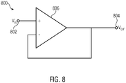
- FIG 8 is a schematic diagram of a buffer amplifier 800 that can be used in the low data rate interface 210 shown in Figure 3 and Figure 4 , according to an embodiment.
- buffer amplifier 800 includes an operational amplifier 806 having a positive input for receiving an input voltage V IN , which is the output voltage of the feature extraction component 208 shown for example in Figure 3 and Figure 4 .
- Operational amplifier 806 also has an output node 804 for generating an output voltage V OUT that is fed back to a negative input to provide a unity gain buffer amplifier configuration.
- Output node 804 is coupled to the output node 216 of the digital microphone 202 shown in Figure 3 and Figure 4 .
- Other types of amplifiers can be used in place of the amplifier 800 shown in Figure 8 , such as amplifiers without feedback.
- Other low data rate interfaces can include additional components other than a single unit gain amplifier.
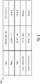
- Figure 9 is a table 900 of clock rates and data rates for various microphone interfaces.
- Table 900 four types of encoding schemes are shown for a digital microphone and the corresponding interface clock rate and data rate at the interface output is shown.
- a comparison related to the amount of data to be transmitted in each of the four types of encoding schemes is represented in Table 900.
- Typical digital microphones provide pulse-density modulation (PDM) data at 768 kHz (for VAD, KWD, and voice recognition applications), which is used as a reference. With pulse-code modulation (PCM) data transmission a data rate reduction of a factor of three can be achieved.
- PDM pulse-density modulation
- PCM pulse-code modulation
- Two clock rates and two data rates are shown for two corresponding feature extraction cases are shown in table 900 for comparison with the PDM and PCM cases previously described.
- Two corner cases (Case 1 and Case 2) are shown in table 900.
- Case 1 forty (40) features are calculated out of frames with 10 ms length and in Case 2, twenty (20) features are calculated out of frames with 20 ms length.
- Table 900 shows that the amount of data at the interface can be reduced significantly if features are transmitted instead of the digital audio signal, according to embodiments described herein.
- an interface clock rate of only 100 Hz (for a 16 bit interface) and a data rate of only 64 kbit per second is needed for transmitting forty features.
- FIG 10 is a block diagram of a low data rate method 1000 associated with a digital microphone, according to an embodiment.
- the low data rate method 1000 can include a conversion method comprising converting an environmental change into an output signal using a MEMS device in method step 1002; extracting a plurality of features from the output signal of the MEMS device in method step 1004; and transmitting the plurality of features through a low data rate interface, wherein a low data rate of the low data rate interface is determined by a number of the plurality of features transmitted, and wherein the conversion method is practiced by one or more integrated circuits in a single semiconductor package in method step 1006.
- FIG 11 is a block diagram of a digital microphone system 1100, according to an embodiment.
- Digital microphone system 1100 includes a digital microphone 1110 including a MEMS device and corresponding ASIC in a single package 1102.
- the MEMS device can comprise an audio microphone for detecting audio signals in the audio band, generally from 20 to 20 KHz, or a pressure detector for detecting pressure signals at the lower end of the audio band or even lower frequency pressure signals.
- the output of MEMS device and corresponding ASIC in package 1102 is coupled to an audio codec 1104, in an embodiment.
- the MEMS device and corresponding ASIC in package 1102 can comprise one or more integrated circuits.
- audio codec 1104 is external to MEMS device and ASIC in package 1102.
- Digital microphone system 1100 also includes a processor 1106 for providing clock signals and control signals to digital microphone 1110, and for receiving data from digital microphone 1100.
- battery 1108 provides power for processor 1106 and digital microphone 1110.
- processor 1106 and digital microphone 1110 can be integrated together on a single integrated circuit, or in two separate integrated circuits.
- product configurations for the digital microphone system 1100 can be used including in cell phones, smart phones, headsets, clocks, and smart speaker product configurations, among numerous other product configurations.
- Advantages of the embodiments described herein include a reduced power consumption (power savings) in the digital microphone (including power reduction due to reduced clock at the interface, and elimination of the overhead needed for high audio quality digital signal processing is not needed), a reduced frequency system clock is possible (which maybe required by customers for certain applications and in certain operating modes), and reduced signal processing complexity in the subsequent digital signal processor (since no decimation filter is required, and no or a reduced amount of feature extraction is required).
- a MEMS device, a feature extraction component, and a low data rate interface are packaged together in a semiconductor package. At least the feature extraction component and the low data rate interface are integrated together in a single integrated circuit in an embodiment.
Landscapes
- Engineering & Computer Science (AREA)
- Physics & Mathematics (AREA)
- Acoustics & Sound (AREA)
- Signal Processing (AREA)
- Chemical & Material Sciences (AREA)
- Analytical Chemistry (AREA)
- Computer Hardware Design (AREA)
- Microelectronics & Electronic Packaging (AREA)
- Circuit For Audible Band Transducer (AREA)
Abstract
Description
- The present invention relates generally to a digital microphone with a low data rate interface and to a corresponding method.
- Digital microphones are used convert audio input signals into corresponding digital output signals. Typical digital microphones include high data rate interfaces including digital signal processing circuitry in order to convert the audio input signals into high quality digital output signals. Due to the always-on nature of the digital microphone and the high power consumption of the digital circuits in the high data rate interface, the use of the digital microphone in portable devices with battery life limitations can be strongly restricted. Manufacturers and customers desire digital microphones with a low data rate interface in order to reduce power and to extend battery life without a significant loss of performance.
- According to an embodiment, A MEMS system includes a MEMS device; a feature extraction component coupled to an output of the MEMS device, wherein the feature extraction component is configured to provide a plurality of features of an output signal of the MEMS device; and a low data rate interface coupled to the feature extraction components, wherein the low data rate interface is configured to transmit the plurality of features of the output signal of the MEMS device, and wherein a low data rate of the low data rate interface is determined by a number of the plurality of features transmitted, wherein the MEMS device, the feature extraction component, and the low data rate interface are packaged together in a semiconductor package.
- According to another embodiment, a conversion method includes converting an environmental change into an output signal using a MEMS device; extracting a plurality of features from the output signal of the MEMS device; and transmitting the plurality of features through a low data rate interface, wherein a low data rate of the low data rate interface is determined by a number of the plurality of features transmitted, and wherein the conversion method is practiced by one or more integrated circuits in a single semiconductor package.
- According to another embodiment, A MEMS system includes a MEMS microphone; a feature extraction component coupled to an output of the MEMS microphone, wherein the feature extraction component is configured to provide a plurality of features of an output signal of the MEMS microphone; a low data rate interface coupled to the feature extraction component, wherein the low data rate interface is configured to transmit the plurality of features of the output signal of the MEMS device, and wherein a low data rate of the low data rate interface is determined by a number of the plurality of features transmitted; and a codec coupled to the low data rate interface for digitally processing the plurality of transmitted features, wherein the MEMS microphone, the feature extraction component, and the low data rate interface are integrated together on one or more integrated circuits in a single semiconductor package.
- For a more complete understanding of the present invention, and the advantages thereof, reference is now made to the following descriptions taken in conjunction with the accompanying drawings, in which:
-
Figure 1A is a block diagram of an exemplary system partitioning of a digital microphone and a codec including keyword detection, voice activity detection, or voice recognition applications; -
Figure 1B is a graph of CMOS interface power versus frequency for the digital microphone and codec ofFigure 1A ; -
Figure 2 is a block diagram of an exemplary system partitioning of a digital microphone and a codec including a decimation filter; -
Figure 3 is a block diagram of a digital microphone with a low data rate interface and a codec according to an embodiment; -
Figure 4 is a more detailed version of the block diagram inFigure 3 , according to an embodiment; -
Figure 5A is a schematic diagram of a feature extraction component including a biquad filter, according to an embodiment; -
Figure 5B is a schematic diagram of an averaging circuit for averaging the output of the feature extraction component shown inFigure 5A , according to an embodiment; -
Figure 6 is a schematic diagram of a feature extraction component including a voltage-controlled oscillator, a counter, and an averaging circuit, according an embodiment; -
Figure 7 is a block diagram of a feature extraction component comprising an auto-correlation component and an averaging circuit, according to an embodiment; -
Figure 8 is a schematic diagram of a buffer amplifier that can be used in the low data rate interface, according to an embodiment; -
Figure 9 is a table of clock rates and data rates for various microphone interfaces; -
Figure 10 is a block diagram of a low data rate method associated with a digital microphone, according to an embodiment; and -
Figure 11 is a block diagram of a digital microphone system, according to an embodiment. - The making and using of the presently preferred embodiments are discussed in detail below. It should be appreciated, however, that the present invention provides many applicable inventive concepts that can be embodied in a wide variety of specific contexts. The specific embodiments discussed are merely illustrative of specific ways to make and use the invention, and do not limit the scope of the invention.
- According to embodiments, a digital microphone system comprises a MEMS device and an Application Specific Integrated Circuit (ASIC) including a feature extraction component and a low data rate interface coupled to the MEMS device. The feature extraction component extracts a plurality of features that highlight the most dominating and discriminating characteristics from the analog output signal of the MEMS devices. In an embodiment, a high quality replica of the analog digital output can be constructed solely from the plurality of features if desired. In other embodiments, the detected features can be used in conjunction with voice recognition applications to initiate or perform various functions. The feature extraction of the feature extraction component can be conducted in the analog or digital domain. In embodiments, the ASIC is coupled to an external audio coder-decoder (codec) that may include one or more applications that include voice activity detection (VAD), keyword detection (KWD), and voice recognition applications. The low data rate of the low data rate interface is advantageously provided by transmitting only a plurality of features from the feature extraction component through the low rate interface to the codec. Typically, the amount of data associated with the transmitted features is much less than the amount of data associated with a digitally converted analog signal using a high clock rate. Thus, the data rate of the digital microphone system can be reduced.
- In some embodiments, the feature extraction is conducted in the analog domain. Thus, an analog-to-digital converter is used to convert the analog features into digital features for subsequent digital signal processing in the digital microphone system. However, the power required to perform the analog-to-digital conversion of the analog features is much lower than the power required to perform a full analog-to-digital conversion of an analog audio signal. The power can be significantly reduced because the clock rate of the analog-to-digital converter can also be significantly reduced. Thus, the digital microphone system according to embodiments can be used in many extremely low power applications. In embodiments, the power requirements of the digital microphone system can be advantageously reduced to less than forty microwatts, preferably less than thirty microwatts, preferably less than twenty microwatts, and preferably less than ten microwatts.
-
Figure 1A is a block diagram of an exemplary system partitioning of adigital microphone system 100A, particularly configured for standard voice recognition applications. Thedigital microphone system 100A includes adigital microphone 102 comprising aMEMS component 104 coupled to an input ofASIC 107 through theanalog output 106 of theMEMS component 104. TheMEMS component 104 can comprise a MEMS microphone component. ASIC 107 includes an analog-to-digital converter (ADC) 108 for converting the analog signal at theanalog output 106 into a digital code. The digital code is typically filtered by adigital filter 110 coupled to the output ofADC 108. Finally, ASIC 107 typically includes a digital modulator into a single bit digital stream at thedigital microphone output 116. ASIC 107 receives a clock signal atclock input 114 to distribute to one or more of the ASICcomponents including ADC 108,digital filter 110, and/ordigital modulator 112.Microphone system 100A typically includes anaudio codec 118 including keyword detection, voice activity detection, or voice recognition applications. Acodec output 124 provides a digital signal with output data generated by the keyword detection, voice activity detection, or voice recognition application. InFigure 1A , the MEMSmicrophone 104 senses acoustic signals and the ASIC 107 transmits a single bit signal to a processor (not shown inFigure 1 ). The single bit signal can be encoded using Pulse Code Modulation (PCM) or Pulse Density Modulation (PDM). Further digital signal processing functionality is performed such as feature extraction inDSP component 120, and the voice activity detection (VAD), keyword detection (KWD) or voice recognition is performed invoice recognition component 122.DSP block 120 has an input coupled to thedigital microphone output 116, andvoice recognition component 122 has an output coupled tocodec output 124. - One aspect of the digital microphone system shown in
Figure 1A is the high power consumption due to the high clock rate used the analog-to-digital conversion performed by ADC 108. A standard digital microphone typically provides a single bit stream at a low data rate (for example 768 kHz in a low power operational mode) or at a high data rate (for example 2.4 to 3 MHz in high performance operational mode). The high performance operational mode leads to high power dissipation in ASIC 107 due to the high clock rate required by ADC 108. -
Figure 1B is a graph of CMOS interface power versus frequency for thedigital microphone 102 andaudio codec 118 ofFigure 1A , wherein "interface power" can be defined as the power required bydigital microphone 102 to provide the single bit digital stream atdigital microphone output 116, which is the interface to further processing circuitry such asaudio codec 118. InFigure 1B a 50 pF load capacitance is assumed atdigital microphone output 116. In state of the art microphones, a power consumption as low as 200 µW is achieved but further power reduction is required for some battery powered applications. InFigure 1B the power dissipation of a CMOS interface is depicted versus activity of the interface for two interface voltages. Afirst line 126 represents interface power versus clock frequency at an interface power supply voltage of 1.8 volts. Asecond line 128 represents interface power versus clock frequency at an interface power supply voltage of 1.2 volts. A reasonably-sized load capacitance of 50 pf is assumed. At higher clock frequencies, with a load capacitor of 50 pf, the power needed for data communication is significant compared to the digital microphone power. Both theclock line 114 and the data line atdigital microphone output 116 define the high power requirements at higher frequencies. At a 768 kHz clock rate, for example, interface power requirements are 120µW (at 1.8 volts) or 56 µW (at 1.2 volts). - What is desired is to reduce the interface data rate and the clock rate significantly, such that the power consumption for the interface can be reduced to single digit µW numbers, which is less than 10 microwatts.
-
Figure 2 is a block diagram of an exemplary system partitioning of adigital microphone system 100B including digital microphone andaudio codec 118.Digital microphone system 100B is similar to previously describeddigital microphone system 100A, except thataudio codec 118 includes adecimation filter 126. In some digital microphone systems include a decimation filter for receiving the single bit digital stream atdigital microphone output 116.Decimation filter 126 implements a method of observing only a periodic portion of the ADC samples, while ignoring the rest. The result is to reduce the sample rate ofADC 108. For example, a decimate-by-4 mode would mean that the total samples passing through thedecimation filter 126 are reduced by a factor of four, while all of the other samples are effectively discarded. Digital filtering usingdecimation filter 126 effectively removes the out-of-band noise from the narrowly defined bandwidth that is set by the decimation ratio. An additional aspect of the digital microphone system configuration shown inFigure 2 is that for the feature extraction the audio signal with full quality is not needed, which leads to additional overhead in the digital microphone (for example the high quality ADC 108) and also in subsequent digital signal processing (for example the decimation filter 126). The additional overhead may also increase the power requirements ofdigital microphone system 100B in high clock rate (high performance) applications. -
Figure 3 is a block diagram of adigital microphone system 200A comprising adigital microphone 202 with a low data rate interface and anaudio codec 218 according to an embodiment.Digital microphone 202 includes a MEMS component such as aMEMS microphone 204, which has ananalog output 206. TheMEMS microphone 204 is coupled toASIC 207. In an embodiment,ASIC 207 comprises afeature extraction component 208, which is configured to extract audio features in the analog or digital domain. Thefeature extraction component 208 shown inFigure 4 can include analog, digital, or combined solutions to provide the feature extraction functionality. Specific embodiments of thefeature extraction component 208 are described below. A low datarate interface component 210 is coupled between thefeature extraction component 208 and theoutput 216 of thedigital microphone 202. A specific embodiment of the low datarate interface component 210 is described below.Digital microphone 202 includes aclock input 214 for receiving a clock signal from a processor (not shown inFigure 3 ). The clock signal is then distributed to thefeature extraction component 208 and/or the lowdata rate interface 210. In an embodiment, thedigital microphone system 200A includes anaudio codec 218 coupled to theoutput 216 ofdigital microphone 202.Audio codec 218 is configured with one or more applications, such as a voice activity detection (VAD), keyword detection (KWD) or voice recognition and generates a corresponding digital signal atcodec output 224.Audio codec 218 is described in further detail below. - "Voice Activity Detection" (VAD) as used herein, is associated with a process to detect voice or speech within an input audio or pressure signal (and might not include keyword or phrase detection). The phrase "voice activity detection" is sometimes also referred to as a "wake-on-voice" process or a "wake-on-speech" process. The phrase "Key Word Spotting ("KWS") or "Keyword Detection" (KWD) may refer to a process that detects a specific spoken word or phrase. The phrase "key word spotting" is also sometimes referred to as a voice trigger. The typical design of a VAD algorithm may include: an initial noise reduction stage, e.g. via spectral subtraction; a calculation of features or quantities from a section of the input signal; and the application of a classification rule to classify the section as speech or non-speech, wherein the classification rule is invoked when a value of the calculated feature or quantity exceeds a predetermined threshold.
- Voice recognition can be used to identify a specific speaker, for example in security applications. Numerous voice recognition algorithms can be used including using Hidden Markov models, dynamic time warping (DTW)-based speech recognition, training neural networks, and "end-to-end" automatic speech recognition techniques using simplified voice models that can be used at low audio frame rates.
- In embodiments,
digital microphone 202 comprises one or more integrated circuits in a semiconductor package. In embodiments, the semiconductor package comprises a metal, plastic, glass, or ceramic casing comprising one or more discrete semiconductor devices or integrated circuits. Any suitable type of semiconductor package can be used. In an embodiment,MEMS microphone 204 comprises a first integrated circuit andASIC 207 comprises a second integrated circuit coupled to the first integrated circuit. In other embodiments, a single integrated circuit comprises a common substrate includingMEMS microphone 204 andASIC 207. In embodiments,audio codec 218 is external todigital microphone 202. - According to embodiments,
digital microphone system 200A shown inFigure 3 advantageously minimizes the additional overhead of the signal processing components shown and described with respect to the exemplarydigital microphone system 100A ofFigure 1A , and the exemplarydigital microphone system 100B ofFigure 1B , and significantly reduces the associated power consumption. In the configuration shown inFigure 3 , the data at theoutput 216 oflow data interface 210 are encoded with the extracted features of the voice/audio signal detected by MEMS microphone 203, whereas in the exemplary digital microphone systems described above the full digital time domain voice/audio signal is applied to the interface. - According to embodiments, all or part of the feature extraction functionality is located in the
digital microphone 202 and the features are transmitted to subsequent processing circuitry. By transmitting only the detected features, the data rate at the interface can be reduced significantly leading to reduced power consumption. Data rates for various encoding techniques are described below with respect the table ofFigure 9 . -
Figure 4 illustrates an embodimentdigital microphone 200B in which feature extraction is performed in the analog domain, and thus an additional analog-to-digital converter 220 is interposed between thefeature extraction component 208 and the lowdata rate interface 210. - In the
audio codec 218, thedecimation filter 126 andfeature extraction component 120 previously shown inFigure 2 may now be removed from the digital signal processing chain, according to embodiments, reducing product costs and reducing power requirements. -
Figure 5A is a schematic diagram of a feature extraction component including abiquad filter 500, according to an embodiment. The feature extraction component ofFigure 5A is suitable for use as the extraction component previously described above. Thebiquad filter 500 includes afirst integrator 508 coupled to asecond integrator 510. Theintegrators input 502 of asummer 506. The output ofsummer 506 is coupled to the input ofintegrator 508. The output ofintegrator 508 is coupled to theoutput node 504 of the biquad filter, y(t). The input ofintegrator 510 is coupled tooutput node 504, and the output ofintegrator 510 is coupled to a negative input ofsummer 506. Theoutput node 504 of the biquad filter is coupled to another negative input ofsummer 506 through anamplifier 512. The gain of the amplifier is set to 1/Q, wherein "Q" is the quality factor of the biquad filter.Biquad filter 500 can be implemented in the analog or digital domain. If implemented in the analog domain, a digital-to-analog conversion is required for converting the analog output ofbiquad filter 500. However, the ADC used for the conversion can be operated with a relatively low sample rate. - The corner frequency of the
integrators amplifier 512 can be adjusted as desired to extract the essential features from the analog signal present at theinput node 502. - The
biquad filter 500 shown inFigure 5A can be implemented using, for example, one or more voltage-controlled oscillators (VCOs) as will be described in further detail below, particularly with respect toFigure 6 . The VCOs produce similar signals obtained from an analog filter, but encoded in the frequency of a square wave instead of in an analog voltage or analog current. In an embodiment, the output signal y(t) provided by the filter is differential, i.e. there is a square wave for the positive signal and another square wave for the negative signal. These square waves are generated in the internal VCOs of the filters as is described in further detail below. To extract the audio feature value of the input signal, an averaging circuit is used. This averaging circuit may comprise a counter counting up with the positive signal and counting down with the negative signal. The absolute value of this counter taken periodically represents the average power of the output of the filter and this can be used as the feature value. One implementation of an averaging circuit is described below with respect toFigure 5B . - An averaging circuit including, for example a counter and an absolute value circuit, is used to average the filtered signal at
node 504, y(t), to produce the useful information for extracting the feature values. A schematic diagram of an averagingcircuit 520 is shown inFigure 5B having acounter 522 coupled toinput node 502, which is thedifferential output nodes biquad filter 500 shown inFigure 5A . The positiveoutput signal node 504P is coupled to the "UP" counter input ofcounter 522, and the negativeoutput signal node 504N is coupled to the "DOWN" counter input ofcounter 522. Thecounter 522 is coupled to afirst register 524.Register 524 also receives a clock signal atnode 526 whose frequency rate determines the update rate of the feature extraction.Register 524 is coupled to anabsolute value circuit 530. In some embodiments, the absolute value may be calculated by simply stripping the sign bit of the output ofregister 524; other methods of determining an absolute value, however, may also be used. In alternative embodiments, other non-linear functions can be applied instead of an absolute value function, such as a squaring function. The absolute value circuit is coupled to anadditional integrator circuit 532.Integrator circuit 532 can be implemented as an accumulator circuit including an arithmetic logic unit (ALU) having a first input coupled to theabsolute value circuit 530, and a second input coupled to an output of the ALU. The integrator circuit is coupled to asecond register 534. The output ofregister 534 is coupled tooutput node 528, which provides the output feature values.Register 534 also receives a clock signal atnode 536 whose frequency rate periodically updates the output feature value atnode 528. In embodiments, any suitable counters can be used forcounter 522 and any suitable registers can be used forregister 524 and forregister 534. Other types of arrangements of the components shown in averagingcircuit 520 may be used, and other types of averaging circuits may also be used. - For the feature extraction of the digital microphone described herein, several different efficient feature extraction algorithms are available. For example, the feature extraction algorithm can be based on autocorrelation coefficients. Another approach is based on a band pass filter bank, implemented with a voltage-controlled oscillator (VCO). VCO and autocorrelation coefficient feature extraction embodiments are described below with respect to
Figure 6 andFigure 7 . -
Figure 6 is a schematic diagram of afeature extraction component 600 including a voltage-controlled oscillator and a counter, according an embodiment. The VCO-basedfeature extraction component 600 is similar in configuration to thebiquad filter 500 shown inFigure 5 . In pertinent part, each of the integrators are implemented with a VCO and counter configuration that is described in further detail below. Thefeature extraction component 600 includes a summer having a positive input coupled toinput node 602 for receiving an analog input signal x(t). The output ofsummer 608 is coupled to afirst integrator 612A. The output offirst integrator 612A is coupled to anamplifier 618A having a gain "G". The output ofamplifier 618A is coupled tooutput node 604 for providing a digital output, y(t). Asecond integrator 612B has an input coupled tooutput node 604 and an output coupled to an input ofamplifier 618B having a gain "G". The output ofamplifier 618B is coupled to a negative input ofsummer 608. The digital output signal y(t) is fed back to another negative input ofsummer 608 throughamplifier 610 having a gain of 1/Q, wherein "Q" is the quality factor of the VCO-basedfeature extraction component 600. The digital output signal y(t) atoutput node 604 is coupled to the input of an averagingcircuit 630, which provides the output feature values atnode 632. Averagingcircuit 630 can be similar to averagingcircuit 520 shown inFigure 5B in an embodiment. However, any suitable averaging circuits can also be used. - The corner frequency of the
integrators amplifiers input node 602. - The
first integrator 612A includes afirst VCO 614A having an output coupled to an "up" counter input ofcounter 616A designated C1. A "down" counter input ofcounter 616A receives aclock signal 606 designated "fo". The output ofcounter 616A is coupled to the input ofamplifier 618A. Thesecond integrator 612B includes asecond VCO 614B having an output coupled to an "up" counter input ofcounter 616B designated C2. A "down" counter input ofcounter 616A receives theclock signal 606 designated "fo". The output ofcounter 616B is coupled to the input ofamplifier 618B. - The VCO implementation shown in
Figure 6 has an advantage of not requiring an analog to digital conversion prior to the filter bank, which operates on the frequency encoded signal (from the VCO). As a consequence, the VCO-based filters behave similar to analog band pass filters but their operation uses digital, frequency encoded signals that are processed by VCO oscillators and digital primitives. - Voice band energy is estimated in the digital domain without requiring an explicit analog-to-digital converter for power estimation, as the signal energy can be measured by counting pulses at the filter output. The
ADC 220 shown inFigure 4 is thus not required in the VCO implementation shown inFigure 6 . The mostly digital nature of the VCO implementation shown inFigure 6 allows the use of a subnanometer semiconductor fabrication technology for all of the digital microphone system electronics. For example, thedigital microphone 202 and theaudio codec 218 shown inFigure 3 andFigure 4 can be integrated together on a single subnanometer integrated circuit having a common substrate. Alternatively,digital microphone 202 can be integrated on a first integrated circuit, andaudio codec 218 can be integrated on a second integrated circuit coupled to the first integrated circuit. -
Figure 7 is a block diagram of afeature extraction component 700 comprising an auto-correlation component, according to an embodiment. In general, the autocorrelation algorithm is a measure of the similarities of the analog or digital signal with a replica copy containing a time lag. In general the autocorrelation based feature extraction comprises an autocorrelation function in combination with a Fast Fourier Transformation (FFT) function. The feature extraction component 700 (without the FFT function) can be implemented in its entirety inside of the digital microphone. However, a part of the autocorrelationfeature extraction component 700 could also be implemented in the audio codec, e.g. the calculation of the autocorrelation coefficients in the digital microphone as well as the FFT function. - The
feature extraction component 700 includes aninput node 702 for receiving ananalog input signal 702. Amultiplier 712 includes a first input for receiving theinput signal 702, x(t). Themultiplier 712 includes asecond input 708 for receiving a time-delayed replica of the input signal, x(t-τ), wherein τ is the delay value. Thus, the output ofmultiplier 712 generates the product of the two input signals, which is equal to x(t) × x(t-τ). The output signal ofmultiplier 712 is averaged over a time interval T by averagingcircuit 716 to generate the autocorrelation signal atoutput node 704. The formula for calculating the autocorrelation coefficient "Ac" is equal to 1/T × ∫ x(t)∗x(t-τ) dt from zero to T, wherein T is the selected time interval. The autocorrelation coefficients "Ac" can be calculated in the analog or digital domain. Averagingcircuit 716 can be similar to averagingcircuit 520 shown inFigure 5B . However, any suitable averaging circuit can also be used. - For every delay τ there is one autocorrelation coefficient (Ac), and the product of the input signal and the delay input signal is averaged over the time interval T. Typical numbers for autocorrelation coefficients for voice applications are 16 to 20 autocorrelation coefficients, wherein 16 to 20 delays "τi" are applied. Typically, the features in the 8 kHz range are calculated (therefore sampled with a 16 KHz clock signal) and for the calculation of the autocorrelation coefficients inter multiples of 1/16 kHz are used as the delays, for example τ1 = 1/16 kHz, τ2 = 2∗11, τ3 = 3∗τ1, ..., τ20 = 20∗τ1.
-
Figure 8 is a schematic diagram of abuffer amplifier 800 that can be used in the lowdata rate interface 210 shown inFigure 3 andFigure 4 , according to an embodiment. In an embodiment,buffer amplifier 800 includes anoperational amplifier 806 having a positive input for receiving an input voltage VIN, which is the output voltage of thefeature extraction component 208 shown for example inFigure 3 andFigure 4 .Operational amplifier 806 also has anoutput node 804 for generating an output voltage VOUT that is fed back to a negative input to provide a unity gain buffer amplifier configuration.Output node 804 is coupled to theoutput node 216 of thedigital microphone 202 shown inFigure 3 andFigure 4 . Other types of amplifiers can be used in place of theamplifier 800 shown inFigure 8 , such as amplifiers without feedback. Other low data rate interfaces can include additional components other than a single unit gain amplifier. -
Figure 9 is a table 900 of clock rates and data rates for various microphone interfaces. In Table 900, four types of encoding schemes are shown for a digital microphone and the corresponding interface clock rate and data rate at the interface output is shown. A comparison related to the amount of data to be transmitted in each of the four types of encoding schemes is represented in Table 900. Typical digital microphones provide pulse-density modulation (PDM) data at 768 kHz (for VAD, KWD, and voice recognition applications), which is used as a reference. With pulse-code modulation (PCM) data transmission a data rate reduction of a factor of three can be achieved. - Two clock rates and two data rates are shown for two corresponding feature extraction cases are shown in table 900 for comparison with the PDM and PCM cases previously described. Two corner cases (
Case 1 and Case 2) are shown in table 900. InCase 1, forty (40) features are calculated out of frames with 10 ms length and inCase 2, twenty (20) features are calculated out of frames with 20 ms length. Table 900 shows that the amount of data at the interface can be reduced significantly if features are transmitted instead of the digital audio signal, according to embodiments described herein. InCase 1, an interface clock rate of only 100 Hz (for a 16 bit interface) and a data rate of only 64 kbit per second is needed for transmitting forty features. InCase 2, an interface clock rate of only 50 Hz (for a 16 bit interface) and a data rate of only 16 kbit per second is needed for transmitting twenty features. Different clock rates will correspond to other data rates, including low data rates equal to 256 kbit per second, 192 kbit per second, 128 kbit per second, or 64 kbit per second. -
Figure 10 is a block diagram of a lowdata rate method 1000 associated with a digital microphone, according to an embodiment. The lowdata rate method 1000 can include a conversion method comprising converting an environmental change into an output signal using a MEMS device inmethod step 1002; extracting a plurality of features from the output signal of the MEMS device inmethod step 1004; and transmitting the plurality of features through a low data rate interface, wherein a low data rate of the low data rate interface is determined by a number of the plurality of features transmitted, and wherein the conversion method is practiced by one or more integrated circuits in a single semiconductor package inmethod step 1006. -
Figure 11 is a block diagram of adigital microphone system 1100, according to an embodiment.Digital microphone system 1100 includes adigital microphone 1110 including a MEMS device and corresponding ASIC in asingle package 1102. In an embodiment, the MEMS device can comprise an audio microphone for detecting audio signals in the audio band, generally from 20 to 20 KHz, or a pressure detector for detecting pressure signals at the lower end of the audio band or even lower frequency pressure signals. The output of MEMS device and corresponding ASIC inpackage 1102 is coupled to anaudio codec 1104, in an embodiment. The MEMS device and corresponding ASIC inpackage 1102 can comprise one or more integrated circuits. In anembodiment audio codec 1104 is external to MEMS device and ASIC inpackage 1102. Whileaudio codec 1104 is shown to be part ofdigital microphone 1110, at least part ofaudio codec 1104 may be included inprocessor 1106, in embodiments.Digital microphone system 1100 also includes aprocessor 1106 for providing clock signals and control signals todigital microphone 1110, and for receiving data fromdigital microphone 1100. In a portable embodiment,battery 1108 provides power forprocessor 1106 anddigital microphone 1110. In embodiments,processor 1106 anddigital microphone 1110 can be integrated together on a single integrated circuit, or in two separate integrated circuits. Various product configurations for thedigital microphone system 1100 can be used including in cell phones, smart phones, headsets, clocks, and smart speaker product configurations, among numerous other product configurations. - Advantages of the embodiments described herein include a reduced power consumption (power savings) in the digital microphone (including power reduction due to reduced clock at the interface, and elimination of the overhead needed for high audio quality digital signal processing is not needed), a reduced frequency system clock is possible (which maybe required by customers for certain applications and in certain operating modes), and reduced signal processing complexity in the subsequent digital signal processor (since no decimation filter is required, and no or a reduced amount of feature extraction is required).
- In conclusion, an implementation of a digital microphone and a digital microphone system has been described herein that implements the analog input signal feature extraction (or at least a part of the feature extraction) and transmits the extracted features instead of a high quality digitally encoded audio signal. In embodiments, a MEMS device, a feature extraction component, and a low data rate interface are packaged together in a semiconductor package. At least the feature extraction component and the low data rate interface are integrated together in a single integrated circuit in an embodiment.
- Example embodiments of the present invention are summarized here. Other embodiments can also be understood from the entirety of the specification and the claims filed herein.
- Example 1. According to an embodiment, a MEMS system includes a MEMS device; a feature extraction component coupled to an output of the MEMS device, wherein the feature extraction component is configured to provide a plurality of features of an output signal of the MEMS device; and a low data rate interface coupled to the feature extraction components, wherein the low data rate interface is configured to transmit the plurality of features of the output signal of the MEMS device, and wherein a low data rate of the low data rate interface is determined by a number of the plurality of features transmitted, wherein the MEMS device, the feature extraction component, and the low data rate interface are packaged together in a semiconductor package.
- Example 2. The MEMS system of Example 1, wherein a total power dissipation of the MEMS system is less than forty microwatts.
- Example 3. The MEMS system of any of the above examples, wherein the MEMS device comprises a first integrated circuit, and the feature extraction component and the low data rate interface are integrated together on a second integrated circuit coupled to the first integrated circuit.
- Example 4. The MEMS system of any of the above examples, wherein the low data rate is equal to 256 kbit per second, 192 kbit per second, 128 kbit per second, or 64 kbit per second.
- Example 5. The MEMS system of any of the above examples, wherein the MEMS device comprises a microphone or a pressure sensor.
- Example 6. The MEMS system of any of the above examples, wherein the feature extraction component comprises a bi-quad filter.
- Example 7. The MEMS system of any of the above examples, wherein the feature extraction component comprises a voltage-controlled oscillator coupled to a counter.
- Example 8. The MEMS system of any of the above examples, wherein the feature extraction component comprises an auto-correlation component.
- Example 9. The MEMS system of any of the above examples, wherein the feature extraction component comprises an input for receiving a clock signal.
- Example 10. The MEMS system of any of the above examples, further comprising an analog-to-digital converter interposed between the feature extraction component and the low data rate interface.
- Example 11. According to an embodiment, a conversion method includes converting an environmental change into an output signal using a MEMS device; extracting a plurality of features from the output signal of the MEMS device; and transmitting the plurality of features through a low data rate interface, wherein a low data rate of the low data rate interface is determined by a number of the plurality of features transmitted, and wherein the conversion method is practiced by one or more integrated circuits in a single semiconductor package.
- Example 12. The conversion method of Example 11, wherein a total power dissipation of the one or more integrated circuits is less than forty microwatts.
- Example 13. The conversion method of any of the above examples, wherein the low data rate is equal to 256 kbit per second, 192 kbit per second, 128 kbit per second, or 64 kbit per second.
- Example 14. The conversion method of any of the above examples, wherein extracting the plurality of features from the output signal of the MEMS device comprises filtering the output signal of the MEMS device, or determining auto-correlation features of the output signal of the MEMS device.
- Example 15. The MEMS system of any of the above examples, wherein the environmental change comprises an audio wave having a frequency in the audio band, or a pressure wave having a frequency below the audio band.
- Example 16. According to an embodiment, a MEMS system includes a MEMS microphone; a feature extraction component coupled to an output of the MEMS microphone, wherein the feature extraction component is configured to provide a plurality of features of an output signal of the MEMS microphone; a low data rate interface coupled to the feature extraction component, wherein the low data rate interface is configured to transmit the plurality of features of the output signal of the MEMS device, and wherein a low data rate of the low data rate interface is determined by a number of the plurality of features transmitted; and a codec coupled to the low data rate interface for digitally processing the plurality of transmitted features, wherein the MEMS microphone, the feature extraction component, and the low data rate interface are integrated together on one or more integrated circuits in a single semiconductor package.
- Example 17. The MEMS system of Example 16, wherein a total power dissipation of the one or more integrated circuits is less than forty microwatts.
- Example 18. The MEMS system of any of the above examples, wherein the codec is configured to provide a voice activity detection function.
- Example 19. The MEMS system of any of the above examples, wherein the codec is configured to provide a keyword detection function.
- Example 20. The MEMS system of any of the above examples, wherein the codec is configured to provide a voice recognition function.
- While this invention has been described with reference to illustrative embodiments, this description is not intended to be construed in a limiting sense. Various modifications and combinations of the illustrative embodiments, as well as other embodiments of the invention, will be apparent to persons skilled in the art upon reference to the description. It is therefore intended that the appended claims encompass any such modifications or embodiments.
Claims (15)
- A MEMS system comprising:a MEMS device;a feature extraction component coupled to an output of the MEMS device, wherein the feature extraction component is configured to provide a plurality of features of an output signal of the MEMS device; anda low data rate interface coupled to the feature extraction components, wherein the low data rate interface is configured to transmit the plurality of features of the output signal of the MEMS device, and wherein a low data rate of the low data rate interface is determined by a number of the plurality of features transmitted,wherein the MEMS device, the feature extraction component, and the low data rate interface are packaged together in a semiconductor package.
- The MEMS system of claim 1, wherein a total power dissipation of the MEMS system is less than forty microwatts.
- The MEMS system of claim 1 or 2, wherein the MEMS device comprises a first integrated circuit, and the feature extraction component and the low data rate interface are integrated together on a second integrated circuit coupled to the first integrated circuit.
- The MEMS system of any of the preceding claims, wherein the low data rate is equal to 256 kbit per second, 192 kbit per second, 128 kbit per second, or 64 kbit per second.
- The MEMS system of any of the preceding claims, wherein the MEMS device comprises a microphone or a pressure sensor.
- The MEMS system of any of the preceding claims, wherein the feature extraction component comprises at least one of a bi-quad filter, of a voltage-controlled oscillator coupled to a counter, of an auto-correlation component, and of an input for receiving a clock signal.
- The MEMS system of any of the preceding claims, further comprising an analog-to-digital converter interposed between the feature extraction component and the low data rate interface.
- A conversion method comprising:converting an environmental change into an output signal using a MEMS device;extracting a plurality of features from the output signal of the MEMS device; andtransmitting the plurality of features through a low data rate interface, wherein a low data rate of the low data rate interface is determined by a number of the plurality of features transmitted, and wherein the conversion method is practiced by one or more integrated circuits in a single semiconductor package.
- The conversion method of claim 8, wherein a total power dissipation of the one or more integrated circuits is less than forty microwatts.
- The conversion method of claim 8 or 9, wherein the low data rate is equal to 256 kbit per second, 192 kbit per second, 128 kbit per second, or 64 kbit per second.
- The conversion method of any of claims 8 to 10, wherein extracting the plurality of features from the output signal of the MEMS device comprises filtering the output signal of the MEMS device, or determining auto-correlation features of the output signal of the MEMS device.
- The MEMS system of any of the preceding claims, wherein the environmental change comprises an audio wave having a frequency in the audio band, or a pressure wave having a frequency below the audio band.
- A MEMS system comprising:a MEMS microphone;a feature extraction component coupled to an output of the MEMS microphone, wherein the feature extraction component is configured to provide a plurality of features of an output signal of the MEMS microphone;a low data rate interface coupled to the feature extraction component, wherein the low data rate interface is configured to transmit the plurality of features of the output signal of the MEMS device, and wherein a low data rate of the low data rate interface is determined by a number of the plurality of features transmitted; anda codec coupled to the low data rate interface for digitally processing the plurality of transmitted features,wherein the MEMS microphone, the feature extraction component, and the low data rate interface are integrated together on one or more integrated circuits in a single semiconductor package.
- The MEMS system of claim 13, wherein a total power dissipation of the one or more integrated circuits is less than forty microwatts.
- The MEMS system of claim 13 or 14, wherein the codec is configured to provide at least one of a voice activity detection function, of a keyword detection function, and of a voice recognition function.
Applications Claiming Priority (1)
| Application Number | Priority Date | Filing Date | Title |
|---|---|---|---|
| US17/106,983 US11582560B2 (en) | 2020-11-30 | 2020-11-30 | Digital microphone with low data rate interface |
Publications (1)
| Publication Number | Publication Date |
|---|---|
| EP4007298A1 true EP4007298A1 (en) | 2022-06-01 |
Family
ID=78789721
Family Applications (1)
| Application Number | Title | Priority Date | Filing Date |
|---|---|---|---|
| EP21210212.3A Pending EP4007298A1 (en) | 2020-11-30 | 2021-11-24 | Digital microphone with low data rate interface |
Country Status (3)
| Country | Link |
|---|---|
| US (1) | US11582560B2 (en) |
| EP (1) | EP4007298A1 (en) |
| CN (1) | CN114584907A (en) |
Citations (1)
| Publication number | Priority date | Publication date | Assignee | Title |
|---|---|---|---|---|
| US20180005636A1 (en) * | 2014-12-23 | 2018-01-04 | Cirrus Logic International Semiconductor Ltd. | Microphone unit comprising integrated speech analysis |
Family Cites Families (1)
| Publication number | Priority date | Publication date | Assignee | Title |
|---|---|---|---|---|
| US9542933B2 (en) * | 2013-03-08 | 2017-01-10 | Analog Devices Global | Microphone circuit assembly and system with speech recognition |
-
2020
- 2020-11-30 US US17/106,983 patent/US11582560B2/en active Active
-
2021
- 2021-11-09 CN CN202111318000.2A patent/CN114584907A/en active Pending
- 2021-11-24 EP EP21210212.3A patent/EP4007298A1/en active Pending
Patent Citations (1)
| Publication number | Priority date | Publication date | Assignee | Title |
|---|---|---|---|---|
| US20180005636A1 (en) * | 2014-12-23 | 2018-01-04 | Cirrus Logic International Semiconductor Ltd. | Microphone unit comprising integrated speech analysis |
Non-Patent Citations (1)
| Title |
|---|
| GUTIERREZ ERIC ET AL: "VCO-based Feature Extraction Architecture for Low Power Speech Recognition Applications", 2019 IEEE 62ND INTERNATIONAL MIDWEST SYMPOSIUM ON CIRCUITS AND SYSTEMS (MWSCAS), IEEE, 4 August 2019 (2019-08-04), pages 1175 - 1178, XP033653032, DOI: 10.1109/MWSCAS.2019.8885088 * |
Also Published As
| Publication number | Publication date |
|---|---|
| US20220174424A1 (en) | 2022-06-02 |
| US11582560B2 (en) | 2023-02-14 |
| CN114584907A (en) | 2022-06-03 |
Similar Documents
| Publication | Publication Date | Title |
|---|---|---|
| EP3000241B1 (en) | Vad detection microphone and method of operating the same | |
| CN111933158B (en) | Microphone unit including integrated speech analysis | |
| US10332544B2 (en) | Microphone and corresponding digital interface | |
| CN108694959B (en) | Voice energy detection | |
| US9111548B2 (en) | Synchronization of buffered data in multiple microphones | |
| CN104252860B (en) | Speech recognition | |
| US9332345B1 (en) | Use of microphone capacitance as a switched capacitor in an input network of a delta-sigma modulator | |
| US9711166B2 (en) | Decimation synchronization in a microphone | |
| CN111465981B (en) | Analog voice activity detector system and method | |
| US11172312B2 (en) | Acoustic activity detecting microphone | |
| US9467774B2 (en) | System and method for a PCM interface for a capacitive signal source | |
| CN105830463A (en) | Vad detection apparatus and method of operating the same | |
| CN106104686B (en) | Methods in Microphone, Microphone-Component, Microphone-Device | |
| US11582560B2 (en) | Digital microphone with low data rate interface | |
| CN114930451B (en) | Background noise estimation and voice activity detection system | |
| CN110310635B (en) | Voice processing circuit and electronic equipment | |
| Yang et al. | Ultra-low-power intelligent acoustic sensing using cochlea-inspired feature extraction and dnn classification | |
| Gruden et al. | Using spectral subtraction for suppression of noise in speech signals with analog integrated circuits | |
| Hellgren | Feedback Cancellation in Hearing Aids with Filtered-X LMS |
Legal Events
| Date | Code | Title | Description |
|---|---|---|---|
| PUAI | Public reference made under article 153(3) epc to a published international application that has entered the european phase |
Free format text: ORIGINAL CODE: 0009012 |
|
| STAA | Information on the status of an ep patent application or granted ep patent |
Free format text: STATUS: THE APPLICATION HAS BEEN PUBLISHED |
|
| AK | Designated contracting states |
Kind code of ref document: A1 Designated state(s): AL AT BE BG CH CY CZ DE DK EE ES FI FR GB GR HR HU IE IS IT LI LT LU LV MC MK MT NL NO PL PT RO RS SE SI SK SM TR |
|
| STAA | Information on the status of an ep patent application or granted ep patent |
Free format text: STATUS: REQUEST FOR EXAMINATION WAS MADE |
|
| 17P | Request for examination filed |
Effective date: 20220628 |
|
| RBV | Designated contracting states (corrected) |
Designated state(s): AL AT BE BG CH CY CZ DE DK EE ES FI FR GB GR HR HU IE IS IT LI LT LU LV MC MK MT NL NO PL PT RO RS SE SI SK SM TR |
|
| STAA | Information on the status of an ep patent application or granted ep patent |
Free format text: STATUS: EXAMINATION IS IN PROGRESS |
|
| 17Q | First examination report despatched |
Effective date: 20230517 |
|
| REG | Reference to a national code |
Ref country code: DE Ref legal event code: R079 Free format text: PREVIOUS MAIN CLASS: H04R0001080000 Ipc: H04R0001040000 |
|
| GRAP | Despatch of communication of intention to grant a patent |
Free format text: ORIGINAL CODE: EPIDOSNIGR1 |
|
| STAA | Information on the status of an ep patent application or granted ep patent |
Free format text: STATUS: GRANT OF PATENT IS INTENDED |
|
| RIC1 | Information provided on ipc code assigned before grant |
Ipc: H04R 1/04 20060101AFI20260312BHEP Ipc: H04R 1/08 20060101ALI20260312BHEP Ipc: H04R 19/00 20060101ALN20260312BHEP Ipc: H04R 19/04 20060101ALN20260312BHEP |
|
| INTG | Intention to grant announced |
Effective date: 20260324 |