EP4007164A1 - Distortion compensation device and distortion compensation method - Google Patents
Distortion compensation device and distortion compensation method Download PDFInfo
- Publication number
- EP4007164A1 EP4007164A1 EP21805228.0A EP21805228A EP4007164A1 EP 4007164 A1 EP4007164 A1 EP 4007164A1 EP 21805228 A EP21805228 A EP 21805228A EP 4007164 A1 EP4007164 A1 EP 4007164A1
- Authority
- EP
- European Patent Office
- Prior art keywords
- sample
- sub
- interpolation
- signal
- dpd
- Prior art date
- Legal status (The legal status is an assumption and is not a legal conclusion. Google has not performed a legal analysis and makes no representation as to the accuracy of the status listed.)
- Withdrawn
Links
- 238000000034 method Methods 0.000 title claims description 16
- 238000005070 sampling Methods 0.000 claims abstract description 153
- 238000012545 processing Methods 0.000 claims abstract description 84
- 230000004044 response Effects 0.000 claims description 10
- 230000003111 delayed effect Effects 0.000 description 32
- 238000004364 calculation method Methods 0.000 description 31
- 238000010586 diagram Methods 0.000 description 21
- 238000005516 engineering process Methods 0.000 description 19
- 230000003446 memory effect Effects 0.000 description 18
- 230000006870 function Effects 0.000 description 16
- 108010076504 Protein Sorting Signals Proteins 0.000 description 13
- 230000005540 biological transmission Effects 0.000 description 13
- 230000008859 change Effects 0.000 description 11
- 239000000969 carrier Substances 0.000 description 8
- 230000000694 effects Effects 0.000 description 7
- 230000002776 aggregation Effects 0.000 description 6
- 238000004220 aggregation Methods 0.000 description 6
- 238000006467 substitution reaction Methods 0.000 description 6
- 230000001934 delay Effects 0.000 description 5
- 230000009467 reduction Effects 0.000 description 5
- 230000003044 adaptive effect Effects 0.000 description 4
- 238000004891 communication Methods 0.000 description 4
- 238000009795 derivation Methods 0.000 description 4
- 238000011156 evaluation Methods 0.000 description 4
- 230000008569 process Effects 0.000 description 3
- 230000004931 aggregating effect Effects 0.000 description 2
- 238000006243 chemical reaction Methods 0.000 description 2
- 230000006872 improvement Effects 0.000 description 2
- 101100421144 Danio rerio selenoo1 gene Proteins 0.000 description 1
- 101100202896 Mus musculus Selenoo gene Proteins 0.000 description 1
- 230000003466 anti-cipated effect Effects 0.000 description 1
- 230000015556 catabolic process Effects 0.000 description 1
- 238000010276 construction Methods 0.000 description 1
- 230000003247 decreasing effect Effects 0.000 description 1
- 238000006731 degradation reaction Methods 0.000 description 1
- 238000012217 deletion Methods 0.000 description 1
- 230000037430 deletion Effects 0.000 description 1
- 230000001419 dependent effect Effects 0.000 description 1
- 230000010354 integration Effects 0.000 description 1
- 238000005259 measurement Methods 0.000 description 1
- 230000007246 mechanism Effects 0.000 description 1
- 238000012986 modification Methods 0.000 description 1
- 230000004048 modification Effects 0.000 description 1
- 230000010355 oscillation Effects 0.000 description 1
- 238000004088 simulation Methods 0.000 description 1
- 230000001629 suppression Effects 0.000 description 1
Images







Classifications
-
- H—ELECTRICITY
- H03—ELECTRONIC CIRCUITRY
- H03F—AMPLIFIERS
- H03F1/00—Details of amplifiers with only discharge tubes, only semiconductor devices or only unspecified devices as amplifying elements
- H03F1/32—Modifications of amplifiers to reduce non-linear distortion
- H03F1/3241—Modifications of amplifiers to reduce non-linear distortion using predistortion circuits
- H03F1/3247—Modifications of amplifiers to reduce non-linear distortion using predistortion circuits using feedback acting on predistortion circuits
-
- H—ELECTRICITY
- H04—ELECTRIC COMMUNICATION TECHNIQUE
- H04B—TRANSMISSION
- H04B1/00—Details of transmission systems, not covered by a single one of groups H04B3/00 - H04B13/00; Details of transmission systems not characterised by the medium used for transmission
- H04B1/02—Transmitters
- H04B1/04—Circuits
- H04B1/0475—Circuits with means for limiting noise, interference or distortion
-
- H—ELECTRICITY
- H03—ELECTRONIC CIRCUITRY
- H03F—AMPLIFIERS
- H03F1/00—Details of amplifiers with only discharge tubes, only semiconductor devices or only unspecified devices as amplifying elements
- H03F1/32—Modifications of amplifiers to reduce non-linear distortion
- H03F1/3241—Modifications of amplifiers to reduce non-linear distortion using predistortion circuits
- H03F1/3258—Modifications of amplifiers to reduce non-linear distortion using predistortion circuits based on polynomial terms
-
- H—ELECTRICITY
- H03—ELECTRONIC CIRCUITRY
- H03F—AMPLIFIERS
- H03F3/00—Amplifiers with only discharge tubes or only semiconductor devices as amplifying elements
- H03F3/189—High-frequency amplifiers, e.g. radio frequency amplifiers
-
- H—ELECTRICITY
- H03—ELECTRONIC CIRCUITRY
- H03F—AMPLIFIERS
- H03F3/00—Amplifiers with only discharge tubes or only semiconductor devices as amplifying elements
- H03F3/20—Power amplifiers, e.g. Class B amplifiers, Class C amplifiers
- H03F3/24—Power amplifiers, e.g. Class B amplifiers, Class C amplifiers of transmitter output stages
-
- H—ELECTRICITY
- H04—ELECTRIC COMMUNICATION TECHNIQUE
- H04B—TRANSMISSION
- H04B1/00—Details of transmission systems, not covered by a single one of groups H04B3/00 - H04B13/00; Details of transmission systems not characterised by the medium used for transmission
- H04B1/02—Transmitters
- H04B1/04—Circuits
- H04B1/0483—Transmitters with multiple parallel paths
-
- H—ELECTRICITY
- H03—ELECTRONIC CIRCUITRY
- H03F—AMPLIFIERS
- H03F2200/00—Indexing scheme relating to amplifiers
- H03F2200/451—Indexing scheme relating to amplifiers the amplifier being a radio frequency amplifier
-
- H—ELECTRICITY
- H04—ELECTRIC COMMUNICATION TECHNIQUE
- H04B—TRANSMISSION
- H04B1/00—Details of transmission systems, not covered by a single one of groups H04B3/00 - H04B13/00; Details of transmission systems not characterised by the medium used for transmission
- H04B1/02—Transmitters
- H04B1/04—Circuits
- H04B2001/0408—Circuits with power amplifiers
- H04B2001/0425—Circuits with power amplifiers with linearisation using predistortion
-
- H—ELECTRICITY
- H04—ELECTRIC COMMUNICATION TECHNIQUE
- H04B—TRANSMISSION
- H04B1/00—Details of transmission systems, not covered by a single one of groups H04B3/00 - H04B13/00; Details of transmission systems not characterised by the medium used for transmission
- H04B1/02—Transmitters
- H04B1/04—Circuits
- H04B2001/0408—Circuits with power amplifiers
- H04B2001/0433—Circuits with power amplifiers with linearisation using feedback
Definitions
- the present disclosure relates to a distortion compensation apparatus and a distortion compensation method that compensate for distortion of a power amplifier in a transmission apparatus such as a base station used in a wireless communication system.
- a transmission apparatus in a wireless communication system includes a power amplifier amplifying power of a transmission signal. While the power amplifier is required to operate in a region as close to saturation as possible for improvement of power efficiency, linearity of the power amplifier and power efficiency are in a trade-off relation.
- the transmission apparatus includes a distortion compensation apparatus in order to enhance linearity and power efficiency simultaneously.
- the distortion compensation apparatus is used for the purpose of suppressing non-linear distortion generated in the power amplifier during high-efficiency operation and reducing an adjacent channel leakage ratio (ACLR) due to non-linear distortion outside a carrier band (out-of-band) and error vector magnitude (EVM) due to non-linear distortion within the carrier band (in-band).
- ACLR adjacent channel leakage ratio
- EVM error vector magnitude
- Schemes used in a distortion compensation apparatus include a digital predistortion (DPD) scheme.
- DPD-based distortion compensation apparatus enhances linearity of an output signal of a power amplifier and thereby suppresses output distortion by previously adding a signal with an inverse characteristic of non-linear distortion of the power amplifier to an input signal of the power amplifier.
- the output distortion of the power amplifier includes not only distortion due to memoryless non-linearity dependent only on an input signal at a certain time but also distortion due to a memory effect occurring due to bias current and an input signal at a timing shifted relative to the input signal at a certain time. Furthermore, the memory effect in the power amplifier becomes more noticeable as the bandwidth of the input signal increases, and performance of the DPD is thereby limited.
- Examples of proposed specific signal processing performed by the DPD in order to compensate for distortion due to the aforementioned memory effect include inverse distortion generation processing based on a series-based scheme such as a Volterra series, a memory polynomial, and a generalized memory polynomial.
- Non Patent Literature 1 and Non Patent Literature 2 propose the memory polynomial structure and the generalized memory polynomial structure.
- the memory polynomial structure is a Volterra series simplified for the purpose of minimizing the number of coefficients in a trade-off relation with compensation performance.
- the generalized memory polynomial structure generalizes and extends a time shift amount of a memory effect term for an input signal at a certain time to a leading term in addition to a lagging term for improvement of performance of the memory polynomial structure.
- Non Patent Literature 2 proposes a generalized memory polynomial model representing a non-linear model of a specific power amplifier based on an actual measurement or a circuit simulation.
- band widening by a factor of 5 to 20 compared with existing 4th generation (4G) is required even in standardization for prerelease 5G Phase 1 in the 3rd Generation Partnership Project (3GPP); and, in particular, 800 MHz is required as a maximum system bandwidth in the submillimeter wave/millimeter wave band.
- 5G Phase 1 it is agreed to aggregate carriers by intra-band contiguous carrier aggregation in order to achieve the system bandwidth of 800 MHz in the submillimeter wave/millimeter wave band. For example, aggregation of eight carriers each having a channel bandwidth (Ch BW) of 100 MHz with a sub-carrier spacing (SCS) of 60 kHz, the number of sub-carriers 1500 to 1584, and an FFT size of 2048 is considered. Alternatively, aggregation of four carriers each having a channel bandwidth of 200 MHz with a sub-carrier spacing of 60 kHz, the number of sub-carriers 3000 to 3168, and an FFT size of 2048 is considered.
- Ch BW channel bandwidth
- SCS sub-carrier spacing
- aggregation of two carriers each having a channel bandwidth of 400 MHz with sub-carrier spacing of 120 kHz, the number of sub-carriers 3000 to 3168, and an FFT size of 4096 is considered.
- the system bandwidth of 800 MHz is achieved by aggregating carriers by intra-band contiguous carrier aggregation as described above, operation at an extremely high sampling frequency of 983.04 MHz is required in order to process a baseband signal in the total bandwidth of 800 MHz after carrier aggregation even when distortion compensation is not performed.
- a maximum operating frequency (referred to as Fmax.) exceeding 1 GHz in the FPGA is an anticipated value achieved by the next 7 nm or 5 nm process or later to be released in the future. Accordingly, under the condition of using an FPGA based on the current process, it is required to employ a two-phase poly-phase structure also in the operation at 983.04 MHz without performing the aforementioned distortion compensation and operate a chain of each phase at 1/2 of the aforementioned sampling frequency 983.04 MHz.
- the 3GPP has introduced scales being an ACLR of a base station (BS) and an adjacent channel interference ratio (ACIR) based on adjacent channel selectivity (ACS) of user equipment (UE) in terms of adjacent channel interference; and as for an ACLR standard for a BS, the ACLR standard of a BS in frequency bands at 24GHz or higher is relaxed to 28 dBc (for a 24.24 to 33.4 GHz band) and 26 dBc (for a 37 to 52.6 GHz band). Therefore, the system bandwidth of 800 MHz may be achieved without assuming distortion compensation exclusively for the ACLR standard based on non-linear distortion outside the carrier band (out-of-band) in the submillimeter wave/millimeter wave band.
- ACIR adjacent channel interference ratio
- ACS adjacent channel selectivity
- UE user equipment
- EVM error vector magnitude
- DL down link
- FR2 frequency range 2
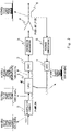
- Fig. 2 is a block diagram illustrating a configuration of a distortion compensation apparatus according to the related art in a transmission apparatus.
- the distortion compensation apparatus includes a digital predistorter (DPD) 1, a digital/analog (DA) converter 2, a transmission upconverter 3, a power amplifier 4, a directional coupler 5, a feedback downconverter 6, an analog/digital (AD) converter 7, and an interpolation circuit 8.
- DPD digital predistorter
- DA digital/analog
- AD analog/digital
- An input signal (baseband signal) x(n) of the distortion compensation apparatus is upsampled by the interpolation circuit 8 in a previous stage of the DPD 1, and upsampled x u (n) is input to the DPD 1.
- the upsampling by the interpolation circuit 8 increases a sampling rate (sampling frequency) of the input signal x(n) and expands the bandwidth of a digital signal for distortion compensation in the DPD 1.
- Setting of the ratio of the operating frequency (sampling frequency) of the DPD 1 to the modulation bandwidth of the input signal x(n) is determined by a multiplying factor of the upsampling by the interpolation circuit 8.
- Upsampling an input signal to a DPD in a previous stage of the DPD and inputting the upsampled signal to the DPD is a technology described in, for example, Patent Literatures 1 and 2.
- a distortion compensation apparatus upsampling an input signal of a DPD in a previous stage of the DPD is hereinafter referred to as an upsampling distortion compensation apparatus as appropriate.
- a DPD to which an upsampled input signal is input in a previous stage thereof in an upsampling distortion compensation apparatus is referred to as an upsampling DPD as appropriate.
- x u (n) acquired by twofold-upsampling, by the interpolation circuit 8 a sampling frequency of 983.04 MHz required for processing an input signal x(n) with a bandwidth of 800 MHz in the aforementioned submillimeter wave/millimeter wave band is input to the DPD 1.
- the operating frequency of the DPD 1 that is, the bandwidth of a digital signal for distortion compensation is 1.96608 GHz being 2.4576 times the bandwidth 800 MHz of the input signal x(n).
- the DPD 1 performs processing (distortion compensation processing) of generating y u (n) by previously adding a signal with an inverse characteristic of non-linear distortion of the power amplifier 4 to input upsampled x u (n) and outputs generated y u (n) to the DA converter 2. Details of the DPD 1 are described later.
- the DA converter 2 DA converts the output signal y u (n) of the DPD 1 from a digital signal into an analog signal and outputs the DA converted analog signal to the transmission upconverter 3.
- the transmission upconverter 3 upconverts an analog signal from the DA converter 2 into a radio frequency (RF) signal and outputs the upconverted RF signal to the power amplifier 4.
- RF radio frequency
- the directional coupler 5 feeds back part of an RF signal being amplified by and being output from the power amplifier 4 and outputs the signal as a feedback RF signal for output observation.
- the feedback RF signal acquired by the directional coupler 5 is fed back to the DPD 1 through the feedback downconverter 6 and the analog/digital (AD) converter 7.
- the feedback downconverter 6 downconverts a feedback RF signal from the directional coupler 5 and outputs the downconverted signal to the AD converter 7.
- the AD converter 7 AD converts a signal from the feedback downconverter 6 from an analog signal into a digital signal and feeds back the AD converted digital signal to the DPD 1 as a feedback signal z u (n).
- the DPD 1 performs the aforementioned distortion compensation processing by using a feedback signal z u (n) from the AD converter 7. Specifically, the DPD 1 includes an LUT and updates the LUT according to the feedback signal z u (n). Then, in the aforementioned distortion compensation processing, the DPD 1 calculates a signal with an inverse characteristic of non-linear distortion of the power amplifier 4 by using the updated LUT and generates y u (n) by adding the calculated signal to x u (n). Details of the LUT are described later.
- an interpolation DAC is used as the DA converter 2 in Fig. 2 (the DA converter 2 is hereinafter referred to as an interpolation DA converter 2 as appropriate) for the purpose of eliminating the need for compensation for a DC offset resulting from imperfection of an analog quadrature modulator and an image caused by a quadrature error, and simplifying a radio circuit.
- the interpolation DA converter is a DA converter incorporating an interpolation function and a digital quadrature modulator function.
- the aforementioned interpolation DA converter is used not only for the purpose of achieving the aforementioned digital quadrature modulation but also as a DA converter even when the digital quadrature modulation is not performed.
- the aforementioned interpolation DA converter can relax required performance of an analog filter required for an output part of a DA converter and is generally used not only as a discrete DA converter but also as a DA converter incorporated in an application-specific general-purpose IC requiring miniaturization and integration, for the purpose of performing over sampling providing a miniaturization effect.
- the aforementioned digital quadrature modulation scheme is a technology described in Non Patent Literature 3.
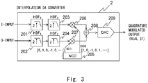
- Fig. 3 is a block diagram illustrating a functional example of the interpolation DA converter 2.
- the interpolation DA converter 2 is configured to provide the digital quadrature modulation function as follows. First, the interpolation DA converter 2 is operated at a sampling clock rate four times the sampling frequency of input I- and Q-signals, and each of the input I- and Q-signals is fourfold interpolated.
- a complex multiplier 206 complex-multiplies the fourfold-interpolated I-signal by an I-phase sine signal (such as 0, 1, 0, -1, 0, ...) from a numerical controlled oscillator (NCO) 205.
- NCO numerical controlled oscillator
- a complex multiplier 207 complex-multiplies the fourfold-interpolated Q-signal by a Q-phase cosine signal (such as 1, 0, -1, 0, 1, ...) from the NCO 205.
- a digital quadrature modulated signal is acquired by adding the signals complex-multiplied by the complex multipliers 206 and 207, respectively, by an adder 208. Then, the digital quadrature modulated signal is converted into an analog signal by one (single-channel) DA conversion unit 209. Thus, a quadrature modulated real intermediate frequency (IF) signal at an IF frequency 1/4 of the sampling clock rate of the interpolation DA converter 2 is output.
- IF real intermediate frequency
- the interpolation DA converter 2 is configured to provide a fourfold interpolation function by connecting two twofold interpolation circuits each zero-stuffing an input signal and then eliminating an image by an interpolation half-band filter.
- the aforementioned half-band filter is used for twofold interpolation or decimation to half in an application for processing a multirate signal. About half of coefficients of the aforementioned half-band filter are equal to zero, and therefore the half-band filter is implemented in a poly-phase form.
- the interpolation DA converter 2 incorporates, as twofold interpolation circuits in an initial stage (first stage), a half-band filter 1 201 and a half-band filter 1 202 for initial-stage twofold interpolation and incorporates, as twofold interpolation circuits in a subsequent stage (second stage), a half-band filter 2 203 and a half-band filter 2 204 for subsequent-stage fourfold interpolation.
- Each of the half-band filters is an interpolation half-band filter with an 80% Nyquist passband.
- Each of the half-band filter 1 201 and the half-band filter 1 202 for initial-stage twofold interpolation is generally a finite impulse response (FIR) filter with 59 taps or so
- each of the half-band filter 2 203 and the half-band filter 2 204 for subsequent-stage fourfold interpolation is an FIR filter with 23 taps or so.
- FIR finite impulse response
- the transmission upconverter 3 in a subsequent stage of the interpolation DA converter 2 has only to convert a real IF signal output from the interpolation DA converter 2 into an RF signal, and an analog quadrature modulator is not required. Accordingly, employment of the interpolation DA converter 2 produces an effect that the radio circuit can be simplified and, furthermore, that processing of compensating for a DC offset resulting from imperfection of an analog quadrature modulator and an image due to a quadrature error can be deleted.
- the interpolation circuit 8 is deleted and upsampling for the DPD 1 is not performed for the purpose of reducing the operating frequency of the DPD 1 itself in order to address the aforementioned second problem related to device performance.
- the operating frequency of the DPD 1 for the input signal bandwidth of 800 MHz in the submillimeter wave/millimeter wave band remains 983.04 MHz being required for processing the input signal x(n) with the 800 MHz bandwidth and being merely 1.2288 times the bandwidth of the input signal x(n), as illustrated in Fig. 6 (details thereof are described later).
- Non Patent Literature 4 proposes a DPD scheme that can narrow the bandwidth of a feedback path in which an AD converter is placed in order to relax a requirement for the AD converter for the purpose of cost reduction of a distortion compensation apparatus.
- Non Patent Literature 4 proposes a DPD scheme that can reduce the sampling frequency of an AD converter for a feedback path to 368.64 MHz by limiting the bandwidth of a feedback signal for output observation of a power amplifier to 100 MHz by a band-pass filter (BPF) for an input signal with a modulation bandwidth of 100 MHz, as illustrated in Fig. 1 .
- BPF band-pass filter
- the technology disclosed in Non Patent Literature 4 operates the DPD at a sampling frequency 3.68 times the bandwidth of the input signal.
- Patent Literature 1 proposes a band-limited Volterra series-based DPD scheme as a means for reducing sampling frequencies of an AD converter for a feedback path, a DA converter for transmission, and a DPD for the purpose of additional cost reduction of a distortion compensation apparatus.
- Patent Literature 1 proposes a DPD scheme that can reduce the sampling frequency of the DPD from 500 MHz according to the related art to 200 MHz with this configuration.
- the technology disclosed in Patent Literature 1 operates the DPD at a sampling frequency twice the bandwidth of the input signal.
- a non-linear processing unit is provided in a previous stage of a bandwidth limitation unit bandwidth-limiting the distortion compensation signal within a pre-set bandwidth.
- the non-linear processing unit needs to generate higher order non-linear distortion and a higher order memory effect for compensation that are not yet limited and are to be output within the bandwidth after bandwidth limitation, based on a Volterra series parameter. Therefore, while the sampling frequency of hardware is reduced to 200 MHz in the non-linear processing unit, high-speed operation is required of a calculation processor in the non-linear processing unit (although not being explicitly described in Patent Literature 1).
- a non-linearity processing calculation processor provided by a microprocessor such as a CPU or an embedded processor is required to operate at a frequency five times the bandwidth of the input signal.
- Patent Literature 2 proposes a DPD subsystem that can improve a distortion compensation characteristic without increasing sampling rates of an AD converter for a feedback path and a DA converter for transmission relative to the related art.
- a DPD subsystem includes a DPD main body, an interpolation circuit placed in a previous stage of the DPD main body as a pre-DPD processor, and a decimation circuit placed in a subsequent stage of the DPD main body as a post-DPD processor.
- This configuration allows sampling rates at the input and the output of the DPD subsystem to be not apparently changed from those according to the related art and allows sampling rates of an AD converter for a feedback path and a DA converter for transmission to be identical to those according to the related art.
- an interpolation circuit is provided in the DPD subsystem, as described above. Therefore, the technology disclosed in Patent Literature 2 is nothing other than a technology for operating the DPD main body at a sampling frequency twice the rate of the input signal even when an interpolation ratio L takes a minimum value of 2.
- Patent Literature 2 can be considered as a bandwidth-limiting DPD in which the interpolation circuit and the decimation circuit based on hardware substitute for the processing performed by the non-linearity processing calculation processor disclosed in Patent Literature 1 in order to perform bandwidth limitation after the aforementioned higher order non-linear distortion and higher order memory effect for compensation in the technology disclosed in Patent Literature 1 are generated.
- the input signal (baseband signal) x(n) of the distortion compensation apparatus illustrated in Fig. 2 is upsampled in the previous stage of the DPD 1 by the interpolation circuit 8, and upsampled x u (n) is input to the DPD 1.
- the upsampling by the interpolation circuit 8 increases the sampling rate (sampling frequency) of the input signal x(n) and expands a digital signal bandwidth for distortion compensation in the DPD 1.
- An upsampling ratio by the interpolation circuit 8 is assumed to be 2
- the operating frequency of the DPD 1 at this time is equal to 2.4576 times the bandwidth 800 MHz of the input signal x(n).
- the DPD 1 generates y u (n) by previously adding a signal with an inverse characteristic of non-linear distortion of the power amplifier 4 to input upsampled x u (n).
- the output signal y u (n) of the DPD 1 is a result of calculating the following equation (1) for the upsampled input signal x u (n) of the DPD 1.
- L is referred to as a memory order or the number of memory taps. Therefore, the time shift amount 1 of the aforementioned memory effect term is hereinafter referred to as a memory tap for convenience.
- Fig. 4 illustrates a block diagram when calculation of the aforementioned equation (4) in the DPD 1 according to the related art is performed by, for example, a hardware function.
- the DPD 1 in Fig. 4 performs calculation of the aforementioned equation (4).
- the DPD 1 in Fig. 4 includes 1-sample delay devices 301a, 301b, 301c, 301d, 301e, and 301f, amplitude address calculation circuits 302a, 302b, 302c, 302d, 302e, 302f, and 302g, look up tables (LUTs) 303a, 303b, 303c, 303d, 303e, 303f, and 303g, complex multipliers 304a, 304b, 304c, 304d, 304e, 304f, and 304g, and an adder 305.
- Fig. 4 is omitted.
- the technique based on the approximation model can be considered as an extended configuration of a related art based on a Wiener-Hammerstein model illustrated in Fig. 2(c) in Non Patent Literature 1, the configuration including three pieces of the model connected in parallel.
- Equation (2) is transformed into an approximation model based on a combination of a polynomial with a reduced number of coefficients and an FIR filter and is expressed by the following equation (5). It is assumed that L (memory order) is reduced from 7 given in the aforementioned equation (3) before reduction in the number of coefficients.
- Equation (5) can be expressed by the following equation (6).
- Equation (6) can be expressed by the following equation (7).
- Equation (8) By delaying n in the equation (7) by three samples, the equation can be expressed by the following equation (8).
- Fig. 5 illustrates a block diagram when calculation of the aforementioned equation (8) in the DPD 1 with a reduced number of coefficients is configured by, for example, a hardware function.
- the DPD 1 in Fig. 5 performs calculation of the aforementioned equation (8).
- the DPD 1 in Fig. 5 includes 1-sample delay devices 401a and 401b, amplitude address calculation circuits 402a, 402b, and 402c, LUTs 403a, 403b, and 403c, complex multipliers 404a, 404b, and 404c, an FIR filter 0 405a, an FIR filter 1 405b, an FIR filter 2 405c, and an adder 406.
- each of the FIR filter 0 405a, the FIR filter 1 405b, and the FIR filter 2 405c includes 1-sample delay devices 411a, 411b, 411c, and 411d, complex multipliers 412a, 412b, 412c, 412d, and 412e, and an adder 413.
- a polynomial x u n ⁇ l S ⁇ K l S x u n ⁇ l S with a reduced number of coefficients at the outputs of the complex multipliers 404a, 404b, and 404c for each term of a memory tap l s in the aforementioned equation (8) is substituted by a function d u (n-l s ) as expressed in the following equation (9) in Fig. 5 .
- x u n ⁇ l S ⁇ K l S x u n ⁇ l S d u n ⁇ l S
- the 1-sample delay devices 401a and 401b From an upsampled input signal x u (n) of the DPD 1 at a certain sampling timing, the 1-sample delay devices 401a and 401b generate x u (n), x u (n-1), and x u (n-2) delayed in steps of one sample.
- the amplitude address calculation circuits 402a, 402b, and 402c calculate LUT amplitude addresses corresponding to amplitudes
- the LUTs 403a, 403b, and 403c are referred to based on the LUT amplitude address for each signal delayed in steps of one sample, and an output signal of each LUT related to the LUT amplitude address is acquired. Then, the complex multipliers 404a, 404b, and 404c complex-multiply the output signals of the LUTs by the signals each delayed in steps of one sample.
- the 1-sample delay devices 411a, 411b, 411c, and 411d generate du(n-l s ), d u (n-l s -1), d u (n-l s -2), d u (n-l s -3), and d u (n-l s -4) delayed in steps of one sample from input d u (n-l s ).
- the output signals of the FIR filter 0 405a, the FIR filter 1 405b, and the FIR filter 2 405c are eventually added by the adder 406 and the added signal is output from the DPD 1 as the polynomial with a reduced number of coefficients expressed by the aforementioned equation (8).
- RMSE root mean square error
- the aforementioned error evaluation function is a normalized root mean square error (NRMSE) as indicated in the following equation (10) and is equivalent to error vector magnitude (EVM) of the feedback signal z u (n) for x u (n).
- an upsampling distortion compensation apparatus based on an interpolation circuit to which the aforementioned equation (8) and the configuration in Fig. 5 are applied is considered.
- the upsampling distortion compensation apparatus based on the interpolation circuit can achieve a 30% reduction in the number of coefficients compared with a DPD to which the aforementioned equation (4) and the configuration in Fig. 4 according to the related art are applied.
- Fig. 6 is a block diagram of a distortion compensation apparatus in which the interpolation circuit 8 illustrated in Fig. 2 is deleted and DPD upsampling is not performed in order to address the second problem of the related art related to device performance in the distortion compensation apparatus.
- FIG. 6 A difference between Fig. 6 and previously described Fig. 2 in terms of configuration is that, with deletion of the interpolation circuit 8, an input signal x(n) not undergoing DPD upsampling directly becomes an input signal of the DPD 1. Further, another difference between Fig. 6 and Fig. 2 in terms of configuration is that while the DPD 1 generates and outputs y(n) acquired by previously adding a signal with an inverse characteristic of non-linear distortion of the power amplifier 4 to input x(n), the sampling frequencies of the output signal y(n) and the input signal x(n) of the DPD 1 are identical.
- the operating frequency of the DPD 1 for a 800 MHz bandwidth of the input signal x(n) in the aforementioned submillimeter wave/millimeter wave band is 983.04 MHz required for processing a baseband input signal in the 800 MHz bandwidth. Therefore, the ratio of the operating frequency of the DPD 1 to the bandwidth of the input signal x(n) is 1.2288, which is less than that of the related art wherein the ratio of the operating frequency of the DPD 1 to the bandwidth of the input signal x(n) is two.
- the input signal x(n) with an 800 MHz bandwidth and the output signal y(n) of the DPD 1 in Fig. 6 are signals sampled at a sampling frequency of 983.04 MHz.
- the maximum frequency of an amplitude envelope change in the input signal x(n) with a modulation bandwidth of 800 MHz is 800 MHz.
- the maximum frequency of an amplitude envelope change in the input signal x(n) is close to the sampling frequency, there is a problem that a change in an amplitude envelope of a signal interpolated by the interpolation DA converter 2 deviates from a change in an amplitude envelope of the signal before interpolation.
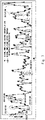
- Fig. 7 illustrates a comparison between amplitude changes of a signal with an 800 MHz bandwidth at a sampling frequency 983.04 MHz before interpolation and amplitude changes of the signal after the signal is twofold-upsampled at a sampling frequency 1.96608 GHz by twofold interpolation processing.
- the aforementioned twofold interpolation processing is processing performed by the initial-stage twofold interpolation circuit zero-stuffing an input signal and then eliminating an image by the interpolation half-band filter in the aforementioned interpolation DA converter 2 illustrated in Fig. 3 .
- a sample point interpolated in a sample spacing of a signal before interpolation is generated by the aforementioned twofold interpolation.
- samples causing considerable deviation between an amplitude envelope change between samples in the signal before the interpolation and an amplitude envelope change of the signal after the twofold interpolation exist (samples causing considerable deviation are surrounded by double broken lines in Fig. 7 ).
- Fig. 8 illustrates a comparison between amplitude changes of a signal twofold-upsampled at a sampling frequency 1.96608 GHz by the aforementioned twofold interpolation processing and amplitude changes of the signal fourfold-upsampled at a sampling frequency 3.93216 GHz by further performing the twofold interpolation processing on the signal.
- the twofold interpolation processing added for the aforementioned fourfold-upsampling is processing performed by the twofold interpolation circuit in the subsequent stage in the aforementioned interpolation DA converter 2 illustrated in Fig. 3 .
- the DPD 1 generates the output signal y(n) of the DPD 1 at a sampling frequency of 983.04 MHz by the input signal x(n) and the feedback signal z(n) at the same sampling frequency.
- an envelope of a modulated signal input to the power amplifier 4 is equal to an envelope of a modulated signal converted into an analog signal after y(n) is interpolated by the interpolation DA converter 2. Therefore, in compensation for distortion generated in the power amplifier 4, a sample point interpolated by the interpolation DA converter 2 needs to be taken into consideration particularly for compensation for a memory effect affected by samples before and after a certain sample point.
- the interpolated sample point is a sub-sample point interpolated between sample points for the DPD 1 operating at a sampling rate before the interpolation and therefore cannot be reflected in a distortion compensation signal for compensation for the memory effect.
- Patent Literature 3 a technology allowing compensation for a memory effect within a carrier band caused by a sub-sample memory tap between sample points in a DPD is proposed in Patent Literature 3.
- the technology disclosed in Patent Literature 3 is described below with reference to drawings.
- Fig. 9 illustrates a block diagram of a configuration example of a DPD 1 disclosed in Patent Literature 3.
- the DPD 1 according to Patent Literature 3 corresponds to the DPD 1 in the distortion compensation apparatus illustrated in Fig. 6 .
- the distortion compensation apparatus illustrated in Fig. 6 has a configuration in which the interpolation circuit 8 in Fig. 2 is deleted and DPD upsampling is not performed, in order to address the aforementioned second problem of the related art related to device performance in the distortion compensation apparatus.
- the distortion compensation apparatus illustrated in Fig. 6 does not perform DPD upsampling processing in the previous stage of the DPD 1 and operates at a non-upsampled and low sampling rate.
- the distortion compensation apparatus illustrated in Fig. 6 can compensate for a memory effect caused by a sub-sample memory tap between sample points in the DPD 1 generated by the interpolation DA converter 2 in the subsequent stage of the DPD 1.
- a signal being generated from a sample signal sequence of non-upsampled input signals of the DPD 1 by pseudo-interpolation and a sub-sample shift and corresponding to twofold-upsampled x u (n-l s ) in the aforementioned equation (8) is denoted by a pseudo-interpolation signal x u '(n-l s ).
- a signal being generated by this x u '(n-l s ) and a sub-sample FIR filter including a sub-sample delay tap and corresponding to the twofold-upsampled y u (n-3) acquired in the aforementioned equation (8) is denoted by y u '(n-3).
- x u (n-l s -r s ) in the aforementioned equation (8) is substituted by x u '(n-l s -r s ), and y u (n-3) is substituted by y u '(n-3).
- Memory taps l s are 0, +1, and +2, and FIR taps r s are 0, +1, +2, +3, and +4 in the equation (11); and each tap represents a twofold-upsampled sample shift amount. Accordingly, the aforementioned memory taps correspond to sub-sample shifts of 0, +0.5, and +1, and the aforementioned FIR taps correspond to sub-sample shifts of 0, +0.5, +1, +1.5, and +2 for the DPD 1 operating at a non-upsampled sampling rate.
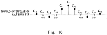
- Fig. 10 illustrates an example of tap coefficients of a twofold-interpolation half-band FIR filter incorporated in the interpolation DA converter 2.
- the center tap of the half-band FIR filter is the i-th tap
- the number of taps is (2i-1)
- tap coefficients are C 1 , C 2 , ..., C i-1 , Ci, C i+1 , ..., and C 2i-1 .
- about half of the tap coefficients of the half-band FIR filter are equal to zero, and the filter is generally configured with 59 taps or so.
- Fig. 10 illustrates only 11 taps including the center tap and the center tap ⁇ 5 taps.
- Fig. 11 illustrates a timing chart illustrating the twofold interpolation processing in the interpolation DA converter 2.
- the twofold interpolation processing is processing of performing zero-stuffing between samplings of the input signal x(n), then eliminating an image through the twofold-interpolation half-band FIR filter illustrated in Fig. 10 , and acquiring a twofold-interpolated output signal x u (n).
- a sampling timing n+1 after the twofold interpolation is a sampling timing at which a sample before the interpolation does not exist. Therefore, in derivation of x u (n+1) at the sampling timing n+1, only i taps other than the center tap and zero-coefficient taps out of (2i-1) taps of the aforementioned twofold-interpolation half-band FIR filter are effective coefficients for the sample signal sequence before the interpolation. Therefore, for example, by using tap coefficients of the 11 taps simplified for the sake of description in Fig. 10 and Fig. 11 , x u (n+1) can be expressed by the following equation (13) for the sample signal sequence before the interpolation.
- x u n + 1 C i ⁇ 5 ⁇ x n ⁇ 2 + C i ⁇ 3 ⁇ x n ⁇ 1 + C i ⁇ 1 ⁇ x n + C i + 1 ⁇ x n + 1 + C i + 3 ⁇ x n + 2 + C i + 5 ⁇ x n + 3
- a sampling timing n-1 after the twofold interpolation is also a sampling timing at which a sample before the interpolation does not exist. Therefore, in derivation of x u (n-1) at the sampling timing n-1, only i taps other than the center tap and the zero-coefficient taps out of the (2i-1) taps of the aforementioned twofold-interpolation half-band FIR filter are effective coefficients for the sample signal sequence before the interpolation. Therefore, for example, by using tap coefficients of the 11 taps simplified for the sake of description in Fig. 10 and Fig. 11 , x u (n-1) can be expressed by the following equation (14) for the sample signal sequence before the interpolation.
- x u n ⁇ 1 C i ⁇ 5 ⁇ x n ⁇ 3 + C i ⁇ 3 ⁇ x n ⁇ 2 + C i ⁇ 1 ⁇ x n ⁇ 1 + C i + 1 ⁇ x n + C i + 3 ⁇ x n + 1 + C i + 5 ⁇ x n + 2
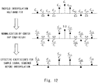
- the purpose of acquiring tap coefficients of the aforementioned pseudo-interpolation filters is not actually performing the twofold interpolation processing illustrated in Fig. 11 on the example of tap coefficients of the twofold-interpolation half-band FIR filter illustrated in Fig. 10 .
- effective coefficients of i taps to be multiplied at the sampling timing before the interpolation are acquired.
- a pseudo-interpolation signal x u '(n+1) can be expressed by the following equation (15).
- a pseudo-interpolation signal x u '(n-1) can be expressed by the following equation (16).
- a pseudo-interpolation/sub-sample-shift filter corresponding to a pseudo-interpolation/sub-sample-shift filter 101b in Fig. 9
- the aforementioned pseudo-interpolation/sub-sample-shift filter has a configuration in which an I-phase tap coefficient and a Q-phase tap coefficient are identical and complex-multiplication is not required.
- sub-sample memory taps ⁇ 0.5 for the DPD 1 operating at the non-upsampled sampling rate are acquired in each path in which the aforementioned pseudo-interpolation/sub-sample-shift filter is placed.
- i denoting the number of taps of the aforementioned pseudo-interpolation/sub-sample-shift filter is an example of the number of taps assumed for (2i-1) taps of the twofold-interpolation half-band FIR filter in the interpolation DA converter 2 but is not restrictive.
- i 30 according to the aforementioned example.
- the number of taps i of the aforementioned pseudo-interpolation/sub-sample-shift filter may be decreased without affecting performance, for the purpose of reducing the circuit size of the aforementioned pseudo-interpolation/sub-sample-shift filter.
- Fig. 13A illustrates an impulse response example of a 0.5-sample delay filter in a case of a delay being a non-integer relative to a sample, for example, the delay being 0.5 samples.
- an impulse response s(n) is an infinite impulse response (IIR) instead of a finite impulse response (FIR), as indicated in the following equation (17).
- IIR infinite impulse response
- FIR finite impulse response
- the circuit size of a filter is reduced by limiting the number of taps to a finite number of taps j.
- an intra-passband ripple occurs.
- processing of multiplication by a window function centered on the delayed point is required.
- the processing involves a narrowed passband, and therefore there is a trade-off relation between the number of taps and a characteristic.
- Fig. 13B illustrates a frequency characteristic of an amount of filter attenuation for the number of taps j when a 0.5-sample delay filter is configured with an FIR filter by limiting the number of tap coefficients to a finite number and performing multiplication by a window function.
- a sub-sample delay filter (corresponding to a sub-sample delay filter 111 in Fig. 9 ) is a filter for distortion compensation within the aforementioned 800 MHz carrier bandwidth. Therefore, when an amount of attenuation at a one-side 400 MHz offset point is to be suppressed to 0.5 dB or less, an example of the number of taps j required for the sub-sample delay filter is 14 taps or more.
- the sub-sample delay filter is a filter simply giving a sub-sample delay. Therefore, when one j-tap 0.5-sample delay filter is provided in one path, a 1.5-sample delay is achievable by placing a 1-sample delay device in a subsequent stage of the 0.5-sample delay filter.
- the aforementioned sub-sample delay filter has a configuration in which an I-phase tap coefficient and a Q-phase tap coefficient are identical and complex-multiplication is not required.
- a signal delayed by 0.5 samples relative to the aforementioned signal delayed by (j/2-1) samples by the aforementioned sub-sample delay filter and a signal delayed by 1.5 samples by further delaying the signal delayed by 0.5 samples by one sample in sampling in the DPD 1 is output.
- a signal delayed by (j/2-1) samples in sampling in the DPD 1 and signals further delayed by one sample and two samples relative to the signal, respectively, in sampling in the DPD 1 is output.
- a signal corresponding to the aforementioned equation (11) can be provided by a polynomial structure with a reduced number of coefficients including a pseudo-interpolation/sub-sample-shift filter and a sub-sample FIR filter including a sub-sample delay filter.
- the calculation corresponding to the equation (19) in which a substitution of a twofold-upsampling rate is made can be achieved by calculating the following equation (20) at a sampling rate of the DPD 1 operating at a non-twofold-upsampled sampling rate.
- the aforementioned equation (20) can be achieved without twofold-upsampling from a sample signal sequence of non-upsampled input signals of the DPD 1 by a polynomial structure including the aforementioned pseudo-interpolation/sub-sample-shift filter and an FIR filter including the aforementioned sub-sample delay filter.
- the DPD 1 according to Patent Literature 3 illustrated in Fig. 9 includes a polynomial structure including the aforementioned pseudo-interpolation/sub-sample-shift filter and an FIR filter being placed in a subsequent stage of the polynomial structure and including the aforementioned sub-sample delay filter.
- Fig. 9 described above illustrates a configuration example of the DPD 1 according to Patent Literature 3 in a case of the calculation of the aforementioned equation (20) being configured by, for example, a hardware function.
- the DPD 1 according to Patent Literature 3 illustrated in Fig. 9 is specifically described below.
- the DPD 1 according to Patent Literature 3 illustrated in Fig. 9 corresponds to the DPD 1 in the distortion compensation apparatus illustrated in Fig. 6.
- Fig. 6 illustrates a configuration example of the distortion compensation apparatus proposed in the present example embodiment.
- the distortion compensation apparatus illustrated in Fig. 6 has a configuration in which the interpolation circuit 8 illustrated in Fig. 2 is deleted and DPD upsampling is not performed, in order to address the aforementioned second problem of the related art related to device performance of the distortion compensation apparatus.
- the DPD 1 according to Patent Literature 3 illustrated in Fig. 9 includes the pseudo-interpolation/sub-sample-shift filters 101a and 101b each configured with an i-tap FIR filter and also includes an i/2-sample delay device 102, a 1-sample delay device 103, amplitude address calculation circuits 104a, 104b, and 104c, LUTs 105a, 105b, and 105c, complex multipliers 106a, 106b, and 106c, an FIR filter 0 107a, an FIR filter 1 107b, an FIR filter 2 107c, and an adder 108.
- each of the FIR filter 0 107a, the FIR filter 1 107b, and the FIR filter 2 107c includes a sub-sample delay filter 111 configured with an j-tap FIR filter and also includes a (j/2-1)-sample delay device 112, 1-sample delay devices 113a, 113b, and 113c, complex multipliers 114a, 114b, 114c, 114d, and 114e, and an adder 115.
- Each of the pseudo-interpolation/sub-sample-shift filters 101a and 101b pseudo-interpolates a sub-sample point between sample points of a signal input to the filter and shifts the pseudo-interpolated sub-sample point by a sub-sample; and each filter is an example of a pseudo-interpolation/sub-sample-shift processing unit.
- the i/2-sample delay device 102 delays a sample point of a signal input to the device by i/2 samples and is an example of a first delay device.
- the amplitude address calculation circuit 104a, the LUT 105a, the complex multiplier 106a, and the FIR filter 0 107a are placed in a subsequent stage of the pseudo-interpolation/sub-sample-shift filter 101a.
- the amplitude address calculation circuit 104b, the LUT 105b, the complex multiplier 106b, and the FIR filter 1 107b are placed in a subsequent stage of the i/2-sample delay device 102.
- the 1-sample delay device 103 is placed in a previous stage of the pseudo-interpolation/sub-sample-shift filter 101b, and the amplitude address calculation circuit 104c, the LUT 105c, the complex multiplier 106c, and the FIR filter 2 107c are placed in a subsequent stage of the pseudo-interpolation/sub-sample-shift filter 101b.
- the 1-sample delay device 103 delays a sample point of a signal input to the device by one sample.
- the adder 108 is placed in a subsequent stage of the FIR filter 0 107a, the FIR filter 1 107b, and the FIR filter 2 107c.
- the adder 108 is an example of a first adder.
- a polynomial structure is defined as a structure from the beginning to the complex multiplier 106a in a path in which the pseudo-interpolation/sub-sample-shift filter 101a is placed. The same applies to other paths.
- each of the FIR filter 0 107a, the FIR filter 1 107b, and the FIR filter 2 107c two paths (second paths) are branched in parallel from an input stage of the FIR filter, and the sub-sample delay filter 111 and the (j/2-1)-sample delay device 112 are placed in the two paths, respectively.
- the sub-sample delay filter 111 delays a sample point of a signal input to the filter by a sub-sample.
- the (j/2-1)-sample delay device 112 delays a sample point of a signal input to the device by (j/2-1) samples and is an example of a second delay device.
- the 1-sample delay devices 113a and 113b connected in series are placed in a subsequent stage of the (j/2-1)-sample delay device 112. Further, the 1-sample delay device 113a is placed in parallel with the complex multiplier 114a in a subsequent stage of the (j/2-1)-sample delay device 112, the 1-sample delay device 113b is placed in parallel with the complex multiplier 114b in a subsequent stage of the 1-sample delay device 113a, and the complex multiplier 114c is placed in a subsequent stage of the 1-sample delay device 113b. The 1-sample delay device 113c is placed in a subsequent stage of the sub-sample delay filter 111.
- the 1-sample delay device 113c is placed in parallel with the complex multiplier 114d in a subsequent stage of the sub-sample delay filter 111, and the complex multiplier 114e is placed in a subsequent stage of the 1-sample delay device 113c.
- Each of the 1-sample delay devices 113a, 113b, and 113c delays a sample point of a signal input to the device by one sample.
- the adder 115 is placed in a subsequent stage of the complex multipliers 114a, 114b, 114c, 114d, and 114e.
- the adder 115 is an example of a second adder.
- the sample amount of each delay described above is a value at the sampling rate of the DPD 1 operating at a non-upsampled sampling rate.
- a polynomial x n ⁇ i 2 + 1 2 ⁇ l S 2 ⁇ K l S x n ⁇ i 2 + 1 2 ⁇ l S 2 at each output of the complex multipliers 106a, 106b, and 106c for each term of the memory tap l s in the aforementioned equation (20) is substituted by a function d n ⁇ i 2 + 1 2 ⁇ l S 2 as expressed by the following equation (21).
- x n ⁇ i 2 + 1 2 ⁇ l S 2 ⁇ K l s x n ⁇ i 2 + 1 2 ⁇ l S 2 d n ⁇ i 2 + 1 2 ⁇ l S 2
- the pseudo-interpolation/sub-sample-shift filter 101a generates x n ⁇ i 2 + 1 2 at the sampling rate of the DPD 1, the signal corresponding to a twofold-interpolated signal x u '(n-i+1) delayed by (i-1) samples in sampling after twofold interpolation, from an input signal x(n) of the DPD 1 at a certain sampling timing.
- the 1-sample delay device 103 and the pseudo-interpolation/sub-sample-shift filter 101b generate x n ⁇ i 2 ⁇ 1 2 at the sampling rate of the DPD 1, the signal corresponding to a twofold-interpolated signal x u '(n-i-1) delayed by (i+1) samples in sampling after twofold interpolation.
- each signal x n ⁇ i 2 + 1 2 , x n ⁇ i 2 , x n ⁇ i 2 ⁇ 1 2 corresponding to delaying in steps of one sample in sampling after twofold interpolation is generated.
- the amplitude address calculation circuits 104a, 104b, and 104c calculate LUT amplitude addresses corresponding to amplitudes x n ⁇ i 2 + 1 2 , x n ⁇ i 2 , x n ⁇ i 2 ⁇ 1 2 of the signals, respectively.
- the LUT 105a, 105b, or 105c is referred to based on a LUT amplitude address for a signal corresponding to delaying in steps of one sample in sampling after the aforementioned twofold interpolation, and an output signal of each LUT related to the LUT amplitude address is acquired. Then, the complex multipliers 106a, 106b, and 106c complex-multiply output signals of the LUTs by signals correspond to delaying in steps of one sample in sampling after the aforementioned twofold interpolation, respectively.
- the (j/2-1)-sample delay device 112 outputs d n ⁇ i 2 + 1 2 ⁇ l S 2 ⁇ j 2 + 1 corresponding to a signal delayed by (j-2) samples in sampling after twofold interpolation.
- the sub-sample delay filter 111 configured with a j-tap FIR filter outputs d n ⁇ i 2 + 1 2 ⁇ l S 2 ⁇ j 2 + 1 2 corresponding to a signal delayed by (j-1) samples in sampling after twofold interpolation.
- the 1-sample delay device 113a in the subsequent stage of the (j/2-1)-sample delay device 112 outputs d n ⁇ i 2 + 1 2 ⁇ l S 2 ⁇ j 2 corresponding to a signal delayed by j samples in sampling after twofold interpolation.
- the 1-sample delay device 113c in the subsequent stage of the sub-sample delay filter 111 outputs d n ⁇ i 2 + 1 2 ⁇ l S 2 ⁇ j 2 ⁇ 1 2 corresponding to a signal delayed by (j+1) samples in sampling after twofold interpolation.
- the 1-sample delay device 113b in the subsequent stage of the 1-sample delay device 113a outputs d n ⁇ i 2 + 1 2 ⁇ l S 2 ⁇ j 2 ⁇ 1 corresponding to a signal delayed by (j+2) samples in sampling after twofold interpolation.
- the signals complex-multiplied by the complex multipliers 114a, 114d, 114b, 114e, and 114c, respectively, are added by the adder 115.
- the output signals of the FIR filter 0 107a, the FIR filter 1 107b, and the FIR filter 2 107c are eventually added by the adder 108, and the added signal is output from the DPD 1 as a polynomial expressed by the aforementioned equation (20) with a reduced number of coefficients.
- the tap coefficients of the pseudo-interpolation/sub-sample-shift filters 101a and 101b and the tap coefficients of the sub-sample delay filter 111 are known fixed coefficients and do not need to be changed.
- the i/2-sample delay device 102 is a fixed delay device determined by the number of taps i of the pseudo-interpolation/sub-sample-shift filters 101a and 101b.
- the (j/2-1)-sample delay device 112 is a fixed delay device determined by the number of taps j of the sub-sample delay filter 111.
- the number of power series coefficients in the LUTs 105a, 105b, and 105c and the number of tap coefficients of the FIR filter 0 107a, the FIR filter 1 107b, and the FIR filter 2 107c that need to be derived and updated by adaptive control are identical to the number of coefficients in the aforementioned equation (8) in which the number of coefficients is reduced by 30% and the configuration illustrated in Fig. 5 , in comparison with the related art.
- x u (n) and z u (n) in the aforementioned equation (10) are substituted by x(n) and z(n), respectively, based on Fig. 6 , in order to adapt to the configuration in which DPD upsampling is not performed.
- the DPD 1 operating at a sampling rate before interpolation by the interpolation DA converter 2 in the subsequent stage of the DPD 1 cannot generate a distortion compensation signal compensating for a memory effect within a carrier band for a sub-sample.
- a distortion compensation signal compensating for a memory effect within the carrier band for a sub-sample for the DPD 1 can be generated by the sub-sample memory taps provided by the pseudo-interpolation/sub-sample-shift filters 101a and 101b and the sub-sample FIR taps provided by the sub-sample delay filter 111.
- the DPD 1 according to Patent Literature 3 illustrated in Fig. 9 is premised on operation at a low sampling rate for sampling an input signal not DPD upsampled in a previous stage of the DPD 1.
- the DPD 1 according to Patent Literature 3 illustrated in Fig. 9 can generate, for example, a signal corresponding to the twofold-upsampled signal x u (n-l s ) in the aforementioned equation (8) with a reduced number of coefficients and Fig. 5 from a sample signal sequence of non-upsampled input signals of the DPD 1.
- the DPD 1 according to Patent Literature 3 illustrated in Fig. 9 can provide, for example, an FIR filter equivalent to the FIR filter 0 405a, the FIR filter 1 405b, and the FIR filter 2 405c in Fig. 5 operating at a twofold sampling frequency.
- the DPD 1 according to Patent Literature 3 illustrated in Fig. 9 not only compensates for distortion due to a sample point but also compensates for distortion due to a sub-sample point between sample points for the DPD 1.
- the distortion compensation apparatus according to Patent Literature 3 illustrated in Fig. 9 is a distortion compensation apparatus operating at a low sampling rate without performing DPD upsampling processing in a previous stage of the DPD 1, the apparatus can reduce an amount of coefficient calculation and can also reduce the operating frequency of the DPD 1 and sampling rates of the DA converter 2 and the AD converter 7, compared with the upsampling distortion compensation apparatus according to the related art. Furthermore, the distortion compensation apparatus can compensate for a memory effect within a carrier band due to a sub-sample memory tap between sample points in the DPD 1 and therefore can achieve target compensation performance.
- Patent Literature 3 mentions an application example of a cross-term configuration in which combinations of complex multiplication of a signal x n ⁇ i 2 + 1 2 ⁇ l S 2 corresponding to delaying in steps of one sample in sampling after twofold interpolation by each LUT output K l S x n ⁇ i 2 + 1 2 ⁇ l S 2 by the complex multipliers 106a, 106b, and 106c are fixed to multiplications of terms with different memory tap l s values.
- an object of the present disclosure is to provide a distortion compensation apparatus and a distortion compensation method that can give a degree of freedom to a combination in a cross-term-based complex multiplication configuration with a small amount of circuit addition without increasing the number of coefficients.
- a distortion compensation apparatus configured to compensate for non-linear distortion of a power amplifier and includes:
- a distortion compensation method is a distortion compensation method by a distortion compensation apparatus configured to compensate for non-linear distortion of a power amplifier and includes:
- the present disclosure produces an effect of providing a distortion compensation apparatus and a distortion compensation method that can give a degree of freedom to a combination in a cross-term-based complex-multiplication configuration with a small amount of circuit addition without increasing the number of coefficients.
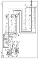
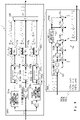
- Fig. 1A and Fig. 1B illustrate block diagrams of a configuration example of a DPD 1 according to the present example embodiment.
- Fig. 1A illustrates a configuration example of the DPD 1 according to the present example embodiment
- Fig. 1B illustrates a configuration example of an FIR filter 0 107a, an FIR filter 1 107b, and an FIR filter 2 107c in the DPD 1 according to the present example embodiment.
- the DPD 1 according to the present example embodiment illustrated in Fig. 1A and Fig. 1B includes a multiplexer 0 109a, a multiplexer 1 109b, and a multiplexer 2 109c in addition to the DPD 1 according to Patent Literature 3 illustrated in Fig. 9 .
- a multiplexer is generally a circuit mechanism selecting or aggregating two or more inputs and outputting one resulting signal.
- Each of the multiplexer 0 109a, the multiplexer 1 109b, and the multiplexer 2 109c according to the present disclosure is a multiplexer as a data selector and, for example, includes three lines of data inputs and one line of a data output.
- Each of the multiplexer 0 109a, the multiplexer 1 109b, and the multiplexer 2 109c selects one line from among the three lines of input signals and set the selected one line as an output signal in accordance with each of selection control signals SELo, SEL 1 , and SEL 2 .
- a memory tap of, in sampling after twofold interpolation, a signal selected by a multiplexer for each path from among the output of the pseudo-interpolation/sub-sample-shift filter 101a, the output of the i/2-sample delay device 102, and the output of the pseudo-interpolation/sub-sample-shift filter 101b, is expressed as m ls .
- One of 0, 1, and 2 is selected as m ls in the example in Fig. 1A and Fig. 1B .
- the LUTs 105a, 105b, and 105c are referred to, and output signals of the LUTs 105a, 105b, and 105c related to the LUT amplitude addresses, respectively, are acquired.
- the complex multipliers 106a, 106b, and 106c complex-multiply the output signals of the LUTs by signals corresponding to delaying in steps of one sample in sampling after twofold interpolation, respectively.
- the output signal of each FIR tap r s corresponding to delaying in steps of one sample in the aforementioned sampling after twofold interpolation is expressed as follows. x n + 3 ⁇ i ⁇ j ⁇ m l S ⁇ r S 2 ⁇ K l S x n + 3 ⁇ i ⁇ j ⁇ l S ⁇ r S 2
- the output signals of the FIR filter 0 107a, the FIR filter 1 107b, and the FIR filter 2 107c are eventually added by an adder 108.
- the result of the addition by the adder 108 corresponds to the equation (20) in the DPD 1 according to Patent Literature 3 illustrated in Fig. 9 and is output from the DPD 1 as a polynomial with a reduced number of coefficients expressed by the following equation (23) in the DPD 1 according to the present example embodiment.
- the distortion compensation apparatus can reduce an amount of coefficient calculation and can reduce the operating frequency of the DPD 1 and the sampling rates of the DA converter 2 and the AD converter 7, compared with the upsampling distortion compensation apparatus according to the related art.
- the number of memory taps l s and m ls , and the number of FIR taps r s indicated in the aforementioned example embodiment are examples and are not restrictive.
- the number of memory taps l s and m ls are set to 3
- the number of FIR taps r s is set to 5 as an example of approximating a seventh-order memory polynomial model in the aforementioned example embodiment
- the seventh-order memory polynomial model may be approximated by setting the number of memory taps l s and m ls to 5 and the number of FIR taps r s to 3. Further, permitting increase in the circuit size and the amount of coefficient calculation, the aforementioned number of taps may be increased.
Landscapes
- Engineering & Computer Science (AREA)
- Power Engineering (AREA)
- Physics & Mathematics (AREA)
- Computer Networks & Wireless Communication (AREA)
- Signal Processing (AREA)
- Nonlinear Science (AREA)
- Algebra (AREA)
- General Physics & Mathematics (AREA)
- Mathematical Analysis (AREA)
- Mathematical Optimization (AREA)
- Pure & Applied Mathematics (AREA)
- Amplifiers (AREA)
Abstract
Description
- The present disclosure relates to a distortion compensation apparatus and a distortion compensation method that compensate for distortion of a power amplifier in a transmission apparatus such as a base station used in a wireless communication system.
- A transmission apparatus in a wireless communication system includes a power amplifier amplifying power of a transmission signal. While the power amplifier is required to operate in a region as close to saturation as possible for improvement of power efficiency, linearity of the power amplifier and power efficiency are in a trade-off relation. Thus, the transmission apparatus includes a distortion compensation apparatus in order to enhance linearity and power efficiency simultaneously. The distortion compensation apparatus is used for the purpose of suppressing non-linear distortion generated in the power amplifier during high-efficiency operation and reducing an adjacent channel leakage ratio (ACLR) due to non-linear distortion outside a carrier band (out-of-band) and error vector magnitude (EVM) due to non-linear distortion within the carrier band (in-band).
- Schemes used in a distortion compensation apparatus include a digital predistortion (DPD) scheme. A DPD-based distortion compensation apparatus enhances linearity of an output signal of a power amplifier and thereby suppresses output distortion by previously adding a signal with an inverse characteristic of non-linear distortion of the power amplifier to an input signal of the power amplifier.
- The output distortion of the power amplifier includes not only distortion due to memoryless non-linearity dependent only on an input signal at a certain time but also distortion due to a memory effect occurring due to bias current and an input signal at a timing shifted relative to the input signal at a certain time. Furthermore, the memory effect in the power amplifier becomes more noticeable as the bandwidth of the input signal increases, and performance of the DPD is thereby limited.
- Examples of proposed specific signal processing performed by the DPD in order to compensate for distortion due to the aforementioned memory effect include inverse distortion generation processing based on a series-based scheme such as a Volterra series, a memory polynomial, and a generalized memory polynomial.
- DPD based on the Volterra series has a problem that it is extremely difficult to implement the DPD on actual hardware since complexity of the DPD increases exponentially in some cases. Therefore, in order to overcome the problem, for example,
Non Patent Literature 1 andNon Patent Literature 2 propose the memory polynomial structure and the generalized memory polynomial structure. The memory polynomial structure is a Volterra series simplified for the purpose of minimizing the number of coefficients in a trade-off relation with compensation performance. The generalized memory polynomial structure generalizes and extends a time shift amount of a memory effect term for an input signal at a certain time to a leading term in addition to a lagging term for improvement of performance of the memory polynomial structure. - A signal processing apparatus performing calculation equivalent to a power series by using a look up table (LUT) is generally proposed as hardware for providing the memory polynomial structure and the generalized memory polynomial structure. Further, for example,
Non Patent Literature 2 proposes a generalized memory polynomial model representing a non-linear model of a specific power amplifier based on an actual measurement or a circuit simulation. However, the generalized memory polynomial model disclosed inNon Patent Literature 2 requires derivation of an inverse system for an extremely large number of non-linear model coefficients at a maximum of 8 (non-linear order: 0 to 7) × 7 (memory order: 7) × 2 (I-phase and Q-phase: 2) = 112. Therefore, the generalized memory polynomial model disclosed inNon Patent Literature 2 has a first problem of the related art that an enormous amount of calculation is still required even when signal processing is performed based on a simplified generalized memory polynomial structure. - Next, a problem involved in changes in technology trends is described.
- In order to achieve high-capacity communication in a 5th generation (5G) wireless communication system, band widening by a factor of 5 to 20 compared with existing 4th generation (4G) is required even in standardization for
prerelease 5G Phase 1 in the 3rd Generation Partnership Project (3GPP); and, in particular, 800 MHz is required as a maximum system bandwidth in the submillimeter wave/millimeter wave band. - In
5G Phase 1, it is agreed to aggregate carriers by intra-band contiguous carrier aggregation in order to achieve the system bandwidth of 800 MHz in the submillimeter wave/millimeter wave band. For example, aggregation of eight carriers each having a channel bandwidth (Ch BW) of 100 MHz with a sub-carrier spacing (SCS) of 60 kHz, the number of sub-carriers 1500 to 1584, and an FFT size of 2048 is considered. Alternatively, aggregation of four carriers each having a channel bandwidth of 200 MHz with a sub-carrier spacing of 60 kHz, the number of sub-carriers 3000 to 3168, and an FFT size of 2048 is considered. Further alternatively, aggregation of two carriers each having a channel bandwidth of 400 MHz with sub-carrier spacing of 120 kHz, the number of sub-carriers 3000 to 3168, and an FFT size of 4096 is considered. However, when the system bandwidth of 800 MHz is achieved by aggregating carriers by intra-band contiguous carrier aggregation as described above, operation at an extremely high sampling frequency of 983.04 MHz is required in order to process a baseband signal in the total bandwidth of 800 MHz after carrier aggregation even when distortion compensation is not performed. - For example, when the aforementioned baseband signal processing is achieved by a field programmable gate array (FPGA), a maximum operating frequency (referred to as Fmax.) exceeding 1 GHz in the FPGA is an anticipated value achieved by the next 7 nm or 5 nm process or later to be released in the future. Accordingly, under the condition of using an FPGA based on the current process, it is required to employ a two-phase poly-phase structure also in the operation at 983.04 MHz without performing the aforementioned distortion compensation and operate a chain of each phase at 1/2 of the aforementioned sampling frequency 983.04 MHz.
- As a 5G standardization trend for the submillimeter wave/millimeter wave band, the 3GPP has introduced scales being an ACLR of a base station (BS) and an adjacent channel interference ratio (ACIR) based on adjacent channel selectivity (ACS) of user equipment (UE) in terms of adjacent channel interference; and as for an ACLR standard for a BS, the ACLR standard of a BS in frequency bands at 24GHz or higher is relaxed to 28 dBc (for a 24.24 to 33.4 GHz band) and 26 dBc (for a 37 to 52.6 GHz band). Therefore, the system bandwidth of 800 MHz may be achieved without assuming distortion compensation exclusively for the ACLR standard based on non-linear distortion outside the carrier band (out-of-band) in the submillimeter wave/millimeter wave band.
- However, an effect on error vector magnitude (EVM) remains in terms of non-linear distortion within a carrier band (in-band). Application of 256 quadrature amplitude modulation (QAM) to a down link (DL) and specification of the EVM standard 3.5% at the time of the application also in the frequency range 2 (FR2) in the submillimeter wave/millimeter wave band are under study toward Release-16 for
next 5G Phase 2 in the 3GPP. In order to satisfy the EVM standard 3.5% for 256 QAM application including an effect of phase noise of a local (local oscillation) signal for a radio circuit in the submillimeter wave/millimeter wave band and EVM degradation involved in an effect of a peak factor suppression signal of a signal, approximately 40 dBc needs to be achieved as signal to noise ratio (SNR) allocation based on non-linear distortion within the carrier band. Therefore, distortion compensation for compensating for non-linear distortion within the carrier band is particularly required. - When distortion compensation is performed, k-th-order non-linearity generally generates a distortion component occupying a bandwidth k times a modulation bandwidth of an input signal (= a maximum frequency of an amplitude envelope change of the input signal). Therefore, DPD compensating for the distortion component across the entire bandwidth is required to operate at a sampling frequency k times the modulation bandwidth of the input signal. For example, an operating frequency (sampling frequency) of approximately 4 GHz is required of DPD compensating for up to fifth-order non-linearity for an input signal bandwidth of 800 MHz in the submillimeter wave/millimeter wave band. Further, even when compensation is limited to third-order or lower non-linearity, an operating frequency of approximately 2.4 GHz is required of the DPD. Therefore, there is a second problem of the related art that the system requirement for the operating frequency of DPD exceeds a performance trend of an actually provided device.
- Next, specific problems of the related art are described with reference to drawings.
-
Fig. 2 is a block diagram illustrating a configuration of a distortion compensation apparatus according to the related art in a transmission apparatus. - As illustrated in
Fig. 2 , the distortion compensation apparatus includes a digital predistorter (DPD) 1, a digital/analog (DA)converter 2, atransmission upconverter 3, apower amplifier 4, adirectional coupler 5, afeedback downconverter 6, an analog/digital (AD)converter 7, and an interpolation circuit 8. - An input signal (baseband signal) x(n) of the distortion compensation apparatus is upsampled by the interpolation circuit 8 in a previous stage of the
DPD 1, and upsampled xu(n) is input to theDPD 1. The upsampling by the interpolation circuit 8 increases a sampling rate (sampling frequency) of the input signal x(n) and expands the bandwidth of a digital signal for distortion compensation in theDPD 1. Setting of the ratio of the operating frequency (sampling frequency) of theDPD 1 to the modulation bandwidth of the input signal x(n) is determined by a multiplying factor of the upsampling by the interpolation circuit 8. - Upsampling an input signal to a DPD in a previous stage of the DPD and inputting the upsampled signal to the DPD is a technology described in, for example,
Patent Literatures - For example, it is assumed that xu(n) acquired by twofold-upsampling, by the interpolation circuit 8, a sampling frequency of 983.04 MHz required for processing an input signal x(n) with a bandwidth of 800 MHz in the aforementioned submillimeter wave/millimeter wave band is input to the
DPD 1. In this case, the operating frequency of theDPD 1, that is, the bandwidth of a digital signal for distortion compensation is 1.96608 GHz being 2.4576 times the bandwidth 800 MHz of the input signal x(n). - The
DPD 1 performs processing (distortion compensation processing) of generating yu(n) by previously adding a signal with an inverse characteristic of non-linear distortion of thepower amplifier 4 to input upsampled xu(n) and outputs generated yu(n) to theDA converter 2. Details of theDPD 1 are described later. - The
DA converter 2 DA converts the output signal yu(n) of theDPD 1 from a digital signal into an analog signal and outputs the DA converted analog signal to thetransmission upconverter 3. - The transmission upconverter 3 upconverts an analog signal from the
DA converter 2 into a radio frequency (RF) signal and outputs the upconverted RF signal to thepower amplifier 4. - The
directional coupler 5 feeds back part of an RF signal being amplified by and being output from thepower amplifier 4 and outputs the signal as a feedback RF signal for output observation. The feedback RF signal acquired by thedirectional coupler 5 is fed back to theDPD 1 through thefeedback downconverter 6 and the analog/digital (AD)converter 7. - The feedback downconverter 6 downconverts a feedback RF signal from the
directional coupler 5 and outputs the downconverted signal to theAD converter 7. - The
AD converter 7 AD converts a signal from thefeedback downconverter 6 from an analog signal into a digital signal and feeds back the AD converted digital signal to theDPD 1 as a feedback signal zu(n). - The
DPD 1 performs the aforementioned distortion compensation processing by using a feedback signal zu(n) from theAD converter 7. Specifically, theDPD 1 includes an LUT and updates the LUT according to the feedback signal zu(n). Then, in the aforementioned distortion compensation processing, theDPD 1 calculates a signal with an inverse characteristic of non-linear distortion of thepower amplifier 4 by using the updated LUT and generates yu(n) by adding the calculated signal to xu(n). Details of the LUT are described later. - In recent years, an interpolation DAC is used as the
DA converter 2 inFig. 2 (theDA converter 2 is hereinafter referred to as aninterpolation DA converter 2 as appropriate) for the purpose of eliminating the need for compensation for a DC offset resulting from imperfection of an analog quadrature modulator and an image caused by a quadrature error, and simplifying a radio circuit. The interpolation DA converter is a DA converter incorporating an interpolation function and a digital quadrature modulator function. - The aforementioned interpolation DA converter is used not only for the purpose of achieving the aforementioned digital quadrature modulation but also as a DA converter even when the digital quadrature modulation is not performed. For example, the aforementioned interpolation DA converter can relax required performance of an analog filter required for an output part of a DA converter and is generally used not only as a discrete DA converter but also as a DA converter incorporated in an application-specific general-purpose IC requiring miniaturization and integration, for the purpose of performing over sampling providing a miniaturization effect.
- For example, the aforementioned digital quadrature modulation scheme is a technology described in
Non Patent Literature 3. -
Fig. 3 is a block diagram illustrating a functional example of theinterpolation DA converter 2. - The
interpolation DA converter 2 is configured to provide the digital quadrature modulation function as follows. First, theinterpolation DA converter 2 is operated at a sampling clock rate four times the sampling frequency of input I- and Q-signals, and each of the input I- and Q-signals is fourfold interpolated. Acomplex multiplier 206 complex-multiplies the fourfold-interpolated I-signal by an I-phase sine signal (such as 0, 1, 0, -1, 0, ...) from a numerical controlled oscillator (NCO) 205. Further, acomplex multiplier 207 complex-multiplies the fourfold-interpolated Q-signal by a Q-phase cosine signal (such as 1, 0, -1, 0, 1, ...) from theNCO 205. Then, a digital quadrature modulated signal is acquired by adding the signals complex-multiplied by thecomplex multipliers adder 208. Then, the digital quadrature modulated signal is converted into an analog signal by one (single-channel) DAconversion unit 209. Thus, a quadrature modulated real intermediate frequency (IF) signal at an IFfrequency 1/4 of the sampling clock rate of theinterpolation DA converter 2 is output. - The
interpolation DA converter 2 is configured to provide a fourfold interpolation function by connecting two twofold interpolation circuits each zero-stuffing an input signal and then eliminating an image by an interpolation half-band filter. - The aforementioned half-band filter is used for twofold interpolation or decimation to half in an application for processing a multirate signal. About half of coefficients of the aforementioned half-band filter are equal to zero, and therefore the half-band filter is implemented in a poly-phase form.
- The
interpolation DA converter 2 incorporates, as twofold interpolation circuits in an initial stage (first stage), a half-band filter 1 201 and a half-band filter 1 202 for initial-stage twofold interpolation and incorporates, as twofold interpolation circuits in a subsequent stage (second stage), a half-band filter 2 203 and a half-band filter 2 204 for subsequent-stage fourfold interpolation. Each of the half-band filters is an interpolation half-band filter with an 80% Nyquist passband. Each of the half-band filter 1 201 and the half-band filter 1 202 for initial-stage twofold interpolation is generally a finite impulse response (FIR) filter with 59 taps or so, and each of the half-band filter 2 203 and the half-band filter 2 204 for subsequent-stage fourfold interpolation is an FIR filter with 23 taps or so. - By employment of the
interpolation DA converter 2, thetransmission upconverter 3 in a subsequent stage of theinterpolation DA converter 2 has only to convert a real IF signal output from theinterpolation DA converter 2 into an RF signal, and an analog quadrature modulator is not required. Accordingly, employment of theinterpolation DA converter 2 produces an effect that the radio circuit can be simplified and, furthermore, that processing of compensating for a DC offset resulting from imperfection of an analog quadrature modulator and an image due to a quadrature error can be deleted. - It is assumed in the distortion compensation apparatus according to the related art illustrated in
Fig. 2 that the interpolation circuit 8 is deleted and upsampling for theDPD 1 is not performed for the purpose of reducing the operating frequency of theDPD 1 itself in order to address the aforementioned second problem related to device performance. With this configuration, for example, the operating frequency of theDPD 1 for the input signal bandwidth of 800 MHz in the submillimeter wave/millimeter wave band remains 983.04 MHz being required for processing the input signal x(n) with the 800 MHz bandwidth and being merely 1.2288 times the bandwidth of the input signal x(n), as illustrated inFig. 6 (details thereof are described later). - Next, difficulty in providing the configuration assumed above in which the interpolation circuit 8 is deleted is described with reference to the related art for comparison.
- An AD converter generally has a relatively lower sampling rate than that of a DA converter and is rate-limiting in terms of performance. Then, for example,
Non Patent Literature 4 proposes a DPD scheme that can narrow the bandwidth of a feedback path in which an AD converter is placed in order to relax a requirement for the AD converter for the purpose of cost reduction of a distortion compensation apparatus. -
Non Patent Literature 4 proposes a DPD scheme that can reduce the sampling frequency of an AD converter for a feedback path to 368.64 MHz by limiting the bandwidth of a feedback signal for output observation of a power amplifier to 100 MHz by a band-pass filter (BPF) for an input signal with a modulation bandwidth of 100 MHz, as illustrated inFig. 1 . However, the technology disclosed inNon Patent Literature 4 operates the DPD at a sampling frequency 3.68 times the bandwidth of the input signal. - On the other hand, for example,
Patent Literature 1 proposes a band-limited Volterra series-based DPD scheme as a means for reducing sampling frequencies of an AD converter for a feedback path, a DA converter for transmission, and a DPD for the purpose of additional cost reduction of a distortion compensation apparatus. - In the technology disclosed in
Patent Literature 1, a distortion compensation signal is generated for an input signal with a modulation bandwidth of 100 MHz by a DPD based on a band-limited Volterra series model. Further, distortion outside the band of a filter bandwidth-limiting the distortion compensation signal generated by the DPD is suppressed by a BPF according to the related art placed in an output part of a power amplifier.Patent Literature 1 proposes a DPD scheme that can reduce the sampling frequency of the DPD from 500 MHz according to the related art to 200 MHz with this configuration. However, the technology disclosed inPatent Literature 1 operates the DPD at a sampling frequency twice the bandwidth of the input signal. - In the technology disclosed in
Patent Literature 1, a non-linear processing unit is provided in a previous stage of a bandwidth limitation unit bandwidth-limiting the distortion compensation signal within a pre-set bandwidth. The non-linear processing unit needs to generate higher order non-linear distortion and a higher order memory effect for compensation that are not yet limited and are to be output within the bandwidth after bandwidth limitation, based on a Volterra series parameter. Therefore, while the sampling frequency of hardware is reduced to 200 MHz in the non-linear processing unit, high-speed operation is required of a calculation processor in the non-linear processing unit (although not being explicitly described in Patent Literature 1). For example, it is assumed that higher order non-linear distortion and a higher order memory effect for compensation equalizing compensation performance within the limited bandwidth with that at the 500 MHz sampling according to the related art are generated. In this case, a non-linearity processing calculation processor provided by a microprocessor such as a CPU or an embedded processor is required to operate at a frequency five times the bandwidth of the input signal. - In addition,
Patent Literature 2 proposes a DPD subsystem that can improve a distortion compensation characteristic without increasing sampling rates of an AD converter for a feedback path and a DA converter for transmission relative to the related art. - In the technology disclosed in
Patent Literature 2, a DPD subsystem includes a DPD main body, an interpolation circuit placed in a previous stage of the DPD main body as a pre-DPD processor, and a decimation circuit placed in a subsequent stage of the DPD main body as a post-DPD processor. This configuration allows sampling rates at the input and the output of the DPD subsystem to be not apparently changed from those according to the related art and allows sampling rates of an AD converter for a feedback path and a DA converter for transmission to be identical to those according to the related art. However, in practice, an interpolation circuit is provided in the DPD subsystem, as described above. Therefore, the technology disclosed inPatent Literature 2 is nothing other than a technology for operating the DPD main body at a sampling frequency twice the rate of the input signal even when an interpolation ratio L takes a minimum value of 2. - Further, the technology disclosed in
Patent Literature 2 can be considered as a bandwidth-limiting DPD in which the interpolation circuit and the decimation circuit based on hardware substitute for the processing performed by the non-linearity processing calculation processor disclosed inPatent Literature 1 in order to perform bandwidth limitation after the aforementioned higher order non-linear distortion and higher order memory effect for compensation in the technology disclosed inPatent Literature 1 are generated. - As described above, for example, in order to perform distortion compensation on an input signal (baseband) with an 800 MHz bandwidth in the aforementioned submillimeter wave/millimeter wave band, 1.6 GHz being twice the bandwidth 800 MHz of the input signal is required as an operating frequency of the DPD even in the technology disclosed in
Patent Literature 1. Further, 1.966 GHz being the bandwidth 800 MHz of an input signal × 2.4576 (= input signal rate 983.04 MHz × 2) is required as an operating frequency of the DPD in the technology disclosed inPatent Literature 2. - Next, in order to illustrate distortion compensation performance of the related art as a reference, a distortion compensation characteristic of the upsampling distortion compensation apparatus illustrated in
Fig. 2 including a twofold interpolation circuit 8 in a previous stage of theDPD 1 for an input signal (= input signal rate 983.04 MHz) with a 800 MHz bandwidth in the aforementioned submillimeter wave/millimeter wave band is described by using a non-linear model of a specific power amplifier. - The input signal (baseband signal) x(n) of the distortion compensation apparatus illustrated in
Fig. 2 is upsampled in the previous stage of theDPD 1 by the interpolation circuit 8, and upsampled xu(n) is input to theDPD 1. The upsampling by the interpolation circuit 8 increases the sampling rate (sampling frequency) of the input signal x(n) and expands a digital signal bandwidth for distortion compensation in theDPD 1. An upsampling ratio by the interpolation circuit 8 is assumed to be 2, and the operating frequency of theDPD 1 is assumed to be the input signal rate 983.04 MHz × 2 = 1.96608 GHz. The operating frequency of theDPD 1 at this time is equal to 2.4576 times the bandwidth 800 MHz of the input signal x(n). - The
DPD 1 generates yu(n) by previously adding a signal with an inverse characteristic of non-linear distortion of thepower amplifier 4 to input upsampled xu(n). - When a generalized memory polynomial structure is applied in the
DPD 1, the output signal yu(n) of theDPD 1 is a result of calculating the following equation (1) for the upsampled input signal xu(n) of theDPD 1.
- A
time shift amount 1 of a memory effect term in the equation (1) is a time shift amount in the unit of a sampling cycle (= 1/sampling frequency) (in other words, a sample shift amount) in the output signal yu(n) of theDPD 1. Furthermore, the aforementioned time shift amount for an input signal at a certain sampling timing is generalized and extended to a leading term in addition to a lagging term in a generalized memory polynomial. Therefore, 1 may take a value from

- Note that L is referred to as a memory order or the number of memory taps. Therefore, the
time shift amount 1 of the aforementioned memory effect term is hereinafter referred to as a memory tap for convenience. - When a power series calculation for each term of the
memory tap 1 in the aforementioned equation (1)

memory tap 1 for each term based on a look up table (LUT) as hardware instead of a direct calculation by a calculation processor, the equation (1) can be expressed by the following equation (2).
- In a term at 1 = 0 in the equation (2), the time shift amount of the output signal of the
DPD 1 relative to the input signal of theDPD 1 is zero. Therefore, a polynomial at 1 = 0 corresponds to a memoryless polynomial. - By specifically giving L = 7 to the aforementioned equation (2) and further making a substitution of l = ls-3 for the
time shift amount 1, the equation (2) can be expressed by the following equation (3).
- By delaying n in the aforementioned equation (3) by three samples, the equation can be expressed by the following equation (4).

- Note that the time shift amount of the output signal of the
DPD 1 relative to the input signal of theDPD 1 is zero in terms at ls = 3 (that is, 1 = 0) in the equation (3) and the equation (4). Therefore, a polynomial at ls = 3 corresponds to a memoryless polynomial. -
Fig. 4 illustrates a block diagram when calculation of the aforementioned equation (4) in theDPD 1 according to the related art is performed by, for example, a hardware function. - The
DPD 1 inFig. 4 performs calculation of the aforementioned equation (4). TheDPD 1 inFig. 4 includes 1-sample delay devices address calculation circuits complex multipliers adder 305. Detailed description ofFig. 4 is omitted. - When the equation (4) and the configuration in
Fig. 4 are applied, assuming a non-linear order to be 0 to 7 and a memory order (the number of memory taps) to be 7, it is required to derive an inverse system for 8 × 7 × 2 = 112 non-linear model coefficients as (I-phase and Q-phase) complex coefficients. - In order to reduce the number of coefficients in addressing the first problem of the aforementioned related art that an enormous amount of calculation is required, a technique for expressing a seventh-order memory polynomial model providing the aforementioned equation (4) and
Fig. 4 by an approximation model based on a combination of a three-tap polynomial and a five-tap FIR filter is introduced. - There is no example of the technique based on the approximation model disclosed in a literature or the like related to the related art. However, the technique based on the approximation model can be considered as an extended configuration of a related art based on a Wiener-Hammerstein model illustrated in Fig. 2(c) in
Non Patent Literature 1, the configuration including three pieces of the model connected in parallel. - The aforementioned equation (2) is transformed into an approximation model based on a combination of a polynomial with a reduced number of coefficients and an FIR filter and is expressed by the following equation (5). It is assumed that L (memory order) is reduced from 7 given in the aforementioned equation (3) before reduction in the number of coefficients.

- Similarly to the aforementioned equation (2), the time shift amount of the output signal of the
DPD 1 relative to the input signal of theDPD 1 is zero in a term at 1 = 0 and r = 0 in the equation (5). Therefore, a polynomial at 1 = 0 and r = 0 corresponds to a memoryless polynomial. - When L = 3 taps and R = 5 taps are given to the aforementioned equation (5) in order to specifically reduce the number of coefficients, the equation (5) can be expressed by the following equation (6).

- Furthermore, by making a substitution of l = ls-1 on the
time shift amount 1 and a substitution of r = rs-2 on r, the equation (6) can be expressed by the following equation (7).
- By delaying n in the equation (7) by three samples, the equation can be expressed by the following equation (8).

- Note that the time shift amount of the output signal of the
DPD 1 relative to the input signal of theDPD 1 is zero in a term at ls = 1 (that is, 1 = 0) and rs = 2 (that is, r = 0) in the equation (7) and the equation (8). Therefore, a polynomial at ls = 1 and rs = 2 corresponds to a memoryless polynomial. -
Fig. 5 illustrates a block diagram when calculation of the aforementioned equation (8) in theDPD 1 with a reduced number of coefficients is configured by, for example, a hardware function. - The
DPD 1 inFig. 5 performs calculation of the aforementioned equation (8). TheDPD 1 inFig. 5 includes 1-sample delay devices address calculation circuits LUTs complex multipliers FIR filter 0 405a, anFIR filter 1 405b, anFIR filter 2 405c, and anadder 406. Furthermore, each of theFIR filter 0 405a, theFIR filter 1 405b, and theFIR filter 2 405c includes 1-sample delay devices complex multipliers adder 413. - For simplification of description, a polynomial

complex multipliers Fig. 5 .
- From an upsampled input signal xu(n) of the
DPD 1 at a certain sampling timing, the 1-sample delay devices address calculation circuits LUTs complex multipliers complex multipliers FIR filter 0 405a, theFIR filter 1 405b, and theFIR filter 2 405c as a polynomial du(n-ls) with a reduced number of coefficients for each term of the memory tap ls = 0, 1, or 2. TheFIR filter 0 405a is related to the memory tap ls = 0. TheFIR filter 1 405b is related to the memory tap ls = 1. TheFIR filter 2 405c is related to the memory tap ls = 2. - In each of the
FIR filter 0 405a,FIR filter 1 405b, andFIR filter 2 405c, the 1-sample delay devices complex multipliers complex multipliers adder 413. The signal added by theadder 413 is output from each of theFIR filter 0 405a, theFIR filter 1 405b, and theFIR filter 2 405c as
- The output signal of the
FIR filter 0 405a related to the memory tap ls = 0 is as follows.
- The output signal of the
FIR filter 1 405b related to the memory tap ls = 1 is as follows.
- The output signal of the
FIR filter 2 405c related to the memory tap ls = 2 is as follows.
- The output signals of the
FIR filter 0 405a, theFIR filter 1 405b, and theFIR filter 2 405c are eventually added by theadder 406 and the added signal is output from theDPD 1 as the polynomial with a reduced number of coefficients expressed by the aforementioned equation (8). - Assuming the non-linear order to be 0 to 7, the memory order (the number of memory taps) to be 3, and the number of FIR taps to be 5 when the equation (8) and the configuration in
Fig. 5 are applied, an inverse system for (8 + 5) × 3 × 2 = 78 non-linear model coefficients may be derived as (I-phase and Q-phase) complex coefficients. Therefore, a 30% reduction in the number of coefficients can be achieved compared with the case of applying the aforementioned equation (4) and the configuration inFig. 4 (the number of coefficients being 112). - The (8 × 3 × 2 = 48) power series coefficients and the (5 × 3 × 2 = 30) tap coefficients of the
FIR filter 0 405a, theFIR filter 1 405b, and theFIR filter 2 405c in theLUTs LUTs reference DPD 1 to the root mean square (RMS) value of the N samples of input signals xu(n) as an error evaluation function. - The aforementioned error evaluation function is a normalized root mean square error (NRMSE) as indicated in the following equation (10) and is equivalent to error vector magnitude (EVM) of the feedback signal zu(n) for xu(n).

-
- Patent Literature 1:
United States Patent No. 9209753 - Patent Literature 2:
United States Patent No. 8537041 - Patent Literature 3:
Japanese Unexamined Patent Application Publication No. 2019-125863 -
- Non Patent Literature 1: D. R. Morgan, Z. Ma, J. Kim, M. G. Zierdt, and J. Pastalan, "A Generalized Memory Polynomial Model for Digital Predistortion of RF Power Amplifiers," IEEE Transactions on Signal Processing, vol. 54, no. 10, pp. 3852-3860, Oct. 2006
- Non Patent Literature 2: 3GPP TR 38.803, V14.1.0 (2017-06), Technical Report, "3rd Generation Partnership Project; Technical Specification Group Radio Access Network; Study on new radio access technology: Radio Frequency (RF) and coexistence aspects," Annex A: PA models
- Non Patent Literature 3: V. Leung, and L. Larson, "Improved Digital-IF Transmitter Architecture for Highly Integrated W-CDMA Mobile Terminals," IEEE Transactions on Vehicular Technology, vol. 54, no. 1, pp. 20-32, Jan. 2005 Non Patent Literature 4: Y. Liu, W. Pan, S. Shao, and Y. Tang, "A New Digital Predistortion for Wideband Power Amplifiers With Constrained Feedback Bandwidth," IEEE Microwave and Wireless Components Letters, vol. 23, no. 12, pp. 683-685, Dec. 2013
- As described above, in order to reduce the number of coefficients for addressing the first problem of the related art that an enormous amount of calculation is required, introduction of an upsampling distortion compensation apparatus based on an interpolation circuit to which the aforementioned equation (8) and the configuration in
Fig. 5 are applied is considered. The upsampling distortion compensation apparatus based on the interpolation circuit can achieve a 30% reduction in the number of coefficients compared with a DPD to which the aforementioned equation (4) and the configuration inFig. 4 according to the related art are applied. - However, twofold-upsampling to 1.96608 GHz is performed by the interpolation circuit 8 in the previous stage of the
DPD 1 in the upsampling distortion compensation apparatus based on the interpolation circuit to which the aforementioned equation (8) and the configuration inFig. 5 are applied, and therefore the system requirement for the operating frequency of theDPD 1 exceeds the performance trend of an actually provided device, as described above. Therefore, the aforementioned second problem remains unsolved. -
Fig. 6 is a block diagram of a distortion compensation apparatus in which the interpolation circuit 8 illustrated inFig. 2 is deleted and DPD upsampling is not performed in order to address the second problem of the related art related to device performance in the distortion compensation apparatus. - A difference between
Fig. 6 and previously describedFig. 2 in terms of configuration is that, with deletion of the interpolation circuit 8, an input signal x(n) not undergoing DPD upsampling directly becomes an input signal of theDPD 1. Further, another difference betweenFig. 6 andFig. 2 in terms of configuration is that while theDPD 1 generates and outputs y(n) acquired by previously adding a signal with an inverse characteristic of non-linear distortion of thepower amplifier 4 to input x(n), the sampling frequencies of the output signal y(n) and the input signal x(n) of theDPD 1 are identical. - Since DPD upsampling is not performed in the case of the configuration illustrated in
Fig. 6 , the operating frequency of theDPD 1 for a 800 MHz bandwidth of the input signal x(n) in the aforementioned submillimeter wave/millimeter wave band is 983.04 MHz required for processing a baseband input signal in the 800 MHz bandwidth. Therefore, the ratio of the operating frequency of theDPD 1 to the bandwidth of the input signal x(n) is 1.2288, which is less than that of the related art wherein the ratio of the operating frequency of theDPD 1 to the bandwidth of the input signal x(n) is two. - Next, a problem of the distortion compensation apparatus with the configuration in
Fig. 6 in which the interpolation circuit 8 is deleted and DPD upsampling is not performed is described. - The input signal x(n) with an 800 MHz bandwidth and the output signal y(n) of the
DPD 1 inFig. 6 are signals sampled at a sampling frequency of 983.04 MHz. The maximum frequency of an amplitude envelope change in the input signal x(n) with a modulation bandwidth of 800 MHz is 800 MHz. However, when the maximum frequency of an amplitude envelope change in the input signal x(n) is close to the sampling frequency, there is a problem that a change in an amplitude envelope of a signal interpolated by theinterpolation DA converter 2 deviates from a change in an amplitude envelope of the signal before interpolation. -
Fig. 7 illustrates a comparison between amplitude changes of a signal with an 800 MHz bandwidth at a sampling frequency 983.04 MHz before interpolation and amplitude changes of the signal after the signal is twofold-upsampled at a sampling frequency 1.96608 GHz by twofold interpolation processing. The aforementioned twofold interpolation processing is processing performed by the initial-stage twofold interpolation circuit zero-stuffing an input signal and then eliminating an image by the interpolation half-band filter in the aforementionedinterpolation DA converter 2 illustrated inFig. 3 . - A sample point interpolated in a sample spacing of a signal before interpolation is generated by the aforementioned twofold interpolation. However, samples causing considerable deviation between an amplitude envelope change between samples in the signal before the interpolation and an amplitude envelope change of the signal after the twofold interpolation exist (samples causing considerable deviation are surrounded by double broken lines in
Fig. 7 ). - Next,
Fig. 8 illustrates a comparison between amplitude changes of a signal twofold-upsampled at a sampling frequency 1.96608 GHz by the aforementioned twofold interpolation processing and amplitude changes of the signal fourfold-upsampled at a sampling frequency 3.93216 GHz by further performing the twofold interpolation processing on the signal. Note that the twofold interpolation processing added for the aforementioned fourfold-upsampling is processing performed by the twofold interpolation circuit in the subsequent stage in the aforementionedinterpolation DA converter 2 illustrated inFig. 3 . - There is no big difference between the amplitude envelope changes of the signal after twofold interpolation and the amplitude envelope changes of the signal after fourfold interpolation.
- The above tells that when the maximum frequency of an amplitude envelope change is close to the sampling frequency (for example, the ratio of the sampling frequency to the bandwidth of the input signal is less than 2), an amplitude envelope change of the interpolated signal deviates from an amplitude envelope change of the signal before the interpolation.
- As described above, when the interpolation circuit is deleted and DPD upsampling is not performed, a problem that deviation in amplitude envelope change occurs between a signal interpolated by the
interpolation DA converter 2 in the subsequent stage of theDPD 1 and a signal before interpolation processed by theDPD 1 is observed. The problem does not need to be considered in the distortion compensation apparatus in which anupsampling DPD 1 based on interpolation according to the related art is employed and twofold or higher upsampling is performed in the previous stage of theDPD 1 and is a problem to be solved unique to the distortion compensation apparatus in which DPD upsampling is not performed. - In
Fig. 6 , theDPD 1 generates the output signal y(n) of theDPD 1 at a sampling frequency of 983.04 MHz by the input signal x(n) and the feedback signal z(n) at the same sampling frequency. However, an envelope of a modulated signal input to thepower amplifier 4 is equal to an envelope of a modulated signal converted into an analog signal after y(n) is interpolated by theinterpolation DA converter 2. Therefore, in compensation for distortion generated in thepower amplifier 4, a sample point interpolated by theinterpolation DA converter 2 needs to be taken into consideration particularly for compensation for a memory effect affected by samples before and after a certain sample point. However, the interpolated sample point is a sub-sample point interpolated between sample points for theDPD 1 operating at a sampling rate before the interpolation and therefore cannot be reflected in a distortion compensation signal for compensation for the memory effect. - The aforementioned problem is specifically described. A memory tap in the equation (8) and the configuration in
Fig. 5 performing the aforementioned twofold-DPD upsampling indicates a sample shift amount in the unit of the sampling cycle (= 1/sampling frequency) after twofold-upsampling at 1.96608 GHz in the previous stage of theDPD 1. Accordingly, for example, a memory tap ls = 1 in the aforementioned equation (8) is a memory tap of a sub-sample corresponding to a memory tap = 0.5 for theDPD 1 operating at a sampling frequency 983.04 MHz in the configuration illustrated inFig. 6 in which the interpolation circuit is deleted and DPD upsampling is not performed.
Therefore, the memory tap ls = 1 is not handled as a memory tap by theDPD 1 operating at the sampling frequency 983.04 MHz and therefore cannot be reflected in a distortion compensation signal for compensation for the memory effect. - As described above, when a configuration in which the interpolation circuit in the previous stage of the DPD is deleted and DPD upsampling is not performed is applied, and the DPD is operated at a sampling frequency 1.2288 times the input signal bandwidth 800 MHz, it is difficult to achieve target compensation performance by the DPD and the distortion compensation apparatus according to the related art.
- Thus, a technology allowing compensation for a memory effect within a carrier band caused by a sub-sample memory tap between sample points in a DPD is proposed in
Patent Literature 3. The technology disclosed inPatent Literature 3 is described below with reference to drawings. -
Fig. 9 illustrates a block diagram of a configuration example of aDPD 1 disclosed inPatent Literature 3. TheDPD 1 according toPatent Literature 3 corresponds to theDPD 1 in the distortion compensation apparatus illustrated inFig. 6 . As described above, the distortion compensation apparatus illustrated inFig. 6 has a configuration in which the interpolation circuit 8 inFig. 2 is deleted and DPD upsampling is not performed, in order to address the aforementioned second problem of the related art related to device performance in the distortion compensation apparatus. - First, an outline of the
DPD 1 according toPatent Literature 3 is described. - As described above, the distortion compensation apparatus illustrated in
Fig. 6 does not perform DPD upsampling processing in the previous stage of theDPD 1 and operates at a non-upsampled and low sampling rate. When the following (A) and (B) are achieved, even the distortion compensation apparatus illustrated inFig. 6 can compensate for a memory effect caused by a sub-sample memory tap between sample points in theDPD 1 generated by theinterpolation DA converter 2 in the subsequent stage of theDPD 1. -
- (A) Generating a signal corresponding to the twofold-upsampled signal xu(n-ls) in the aforementioned equation (8) and
Fig. 5 in which the number of coefficients is reduced, from a sample signal sequence of non-upsampled input signals of theDPD 1. - (B) Providing, without twofold-upsampling, an FIR filter equivalent to the
FIR filter 0 405a, theFIR filter 1 405b, and theFIR filter 2 405c illustrated inFig. 5 operating at the twofold sampling frequency. - In the following equation (11), a signal being generated from a sample signal sequence of non-upsampled input signals of the
DPD 1 by pseudo-interpolation and a sub-sample shift and corresponding to twofold-upsampled xu(n-ls) in the aforementioned equation (8) is denoted by a pseudo-interpolation signal xu'(n-ls). Further, in the following equation (11), a signal being generated by this xu'(n-ls) and a sub-sample FIR filter including a sub-sample delay tap and corresponding to the twofold-upsampled yu(n-3) acquired in the aforementioned equation (8) is denoted by yu'(n-3). Furthermore, in the following equation (11), xu(n-ls-rs) in the aforementioned equation (8) is substituted by xu'(n-ls-rs), and yu(n-3) is substituted by yu'(n-3). A means for achieving the following equation (11) without twofold-upsampling is described below.
- Memory taps ls are 0, +1, and +2, and FIR taps rs are 0, +1, +2, +3, and +4 in the equation (11); and each tap represents a twofold-upsampled sample shift amount. Accordingly, the aforementioned memory taps correspond to sub-sample shifts of 0, +0.5, and +1, and the aforementioned FIR taps correspond to sub-sample shifts of 0, +0.5, +1, +1.5, and +2 for the
DPD 1 operating at a non-upsampled sampling rate. - First, a means for generating xu'(n-ls) corresponding to the memory taps ls = 0, +1, and +2 at the FIR tap rs = 0 in the aforementioned equation (11) from a sample signal sequence of non-upsampled input signals of the
DPD 1 is described. -
Fig. 10 illustrates an example of tap coefficients of a twofold-interpolation half-band FIR filter incorporated in theinterpolation DA converter 2. - It is assumed that the center tap of the half-band FIR filter is the i-th tap, the number of taps is (2i-1), and tap coefficients are C1, C2, ..., Ci-1, Ci, Ci+1, ..., and C2i-1. As described above, about half of the tap coefficients of the half-band FIR filter are equal to zero, and the filter is generally configured with 59 taps or so. For simplification of illustration and description,
Fig. 10 illustrates only 11 taps including the center tap and the center tap ±5 taps. -
Fig. 11 illustrates a timing chart illustrating the twofold interpolation processing in theinterpolation DA converter 2. - For example, assuming a signal before interpolation to be an input signal x(n), the twofold interpolation processing is processing of performing zero-stuffing between samplings of the input signal x(n), then eliminating an image through the twofold-interpolation half-band FIR filter illustrated in
Fig. 10 , and acquiring a twofold-interpolated output signal xu(n). - As described above, the twofold interpolation processing is processing of performing zero-stuffing between samplings before interpolation and then make the signal pass through the half-band FIR filter. Therefore, in derivation of a twofold-interpolated sample xu(n) at a certain sampling timing n at which a sample before interpolation exists, only the center tap coefficient Ci of the aforementioned twofold-interpolation half-band FIR filter is an effective coefficient for a sample signal sequence before the interpolation. Therefore, xu(n) can be expressed by the following equation (12) for the sample signal sequence before the interpolation.

- Next, unlike the aforementioned sampling timing n, a sampling timing n+1 after the twofold interpolation is a sampling timing at which a sample before the interpolation does not exist. Therefore, in derivation of xu(n+1) at the sampling timing n+1, only i taps other than the center tap and zero-coefficient taps out of (2i-1) taps of the aforementioned twofold-interpolation half-band FIR filter are effective coefficients for the sample signal sequence before the interpolation. Therefore, for example, by using tap coefficients of the 11 taps simplified for the sake of description in
Fig. 10 andFig. 11 , xu(n+1) can be expressed by the following equation (13) for the sample signal sequence before the interpolation.
- Furthermore, unlike the aforementioned sampling timing n, a sampling timing n-1 after the twofold interpolation is also a sampling timing at which a sample before the interpolation does not exist. Therefore, in derivation of xu(n-1) at the sampling timing n-1, only i taps other than the center tap and the zero-coefficient taps out of the (2i-1) taps of the aforementioned twofold-interpolation half-band FIR filter are effective coefficients for the sample signal sequence before the interpolation. Therefore, for example, by using tap coefficients of the 11 taps simplified for the sake of description in
Fig. 10 andFig. 11 , xu(n-1) can be expressed by the following equation (14) for the sample signal sequence before the interpolation.
- Next,
Fig. 12 illustrates a procedure for acquiring tap coefficients of a pseudo-interpolation filter (corresponding to pseudo-interpolation/sub-sample-shift filters Fig. 9 ) for acquiring sub-sample memory taps = ±0.5 for theDPD 1 operating at a non-upsampled sampling rate, the tap coefficients being indicated in the aforementioned equation (13) and equation (14). - The purpose of acquiring tap coefficients of the aforementioned pseudo-interpolation filters is not actually performing the twofold interpolation processing illustrated in
Fig. 11 on the example of tap coefficients of the twofold-interpolation half-band FIR filter illustrated inFig. 10 . The purpose of acquiring tap coefficients of the aforementioned pseudo-interpolation filters is acquiring effective coefficients multiplied by a sample signal sequence of input signals of theDPD 1 before interpolation at a sampling timing before the interpolation in order to acquire sub-sample memory taps = ±0.5 for theDPD 1 operating at a non-upsampled sampling rate. - At a sampling timing at which a sample before interpolation exists, every coefficient is normalized by the center tap coefficient Ci in such a way that xu(n) = x(n) (in other words, Ci = 1.0) in the aforementioned equation (12) holds, and then the center tap and zero-coefficient taps are removed. Thus, effective coefficients of i taps to be multiplied at the sampling timing before the interpolation are acquired. The acquired effective coefficients are tap coefficients of an i-tap pseudo-interpolation filter for acquiring sub-sample memory taps = ±0.5 for the
DPD 1 operating at the non-upsampled sampling rate. - Accordingly, by normalizing every coefficient in the aforementioned equation (13) by the center tap coefficient Ci, a pseudo-interpolation signal xu'(n+1) can be expressed by the following equation (15). Furthermore, by normalizing every coefficient in the aforementioned equation (14) by the center tap coefficient Ci, a pseudo-interpolation signal xu'(n-1) can be expressed by the following equation (16).


- A processing delay of the aforementioned i-tap pseudo-interpolation filter is (i-1) samples in sampling after twofold interpolation, that is, (i/2-0.5) converted to sampling in the
DPD 1 operating at the non-upsampled sampling rate. Therefore, when i/2 samples are delayed relative to the input in sampling in theDPD 1 in a path related to a sub-sample memory tap = 0 in which the aforementioned pseudo-interpolation filter is not placed, the aforementioned pseudo-interpolation filter in a path in which the aforementioned pseudo-interpolation filter is placed is a pseudo-interpolation/sub-sample-shift filter (corresponding to a pseudo-interpolation/sub-sample-shift filter 101a inFig. 9 ) for acquiring a sub-sample memory tap ahead of the aforementioned path related to the sub-sample memory tap = 0 by 0.5 samples, that is, a sub-sample memory tap = -0.5 for theDPD 1. Further, when the aforementioned pseudo-interpolation filter is placed after one sample is delayed relative to the input in sampling in theDPD 1, the aforementioned pseudo-interpolation filter placed after the aforementioned 1-sample delay is a pseudo-interpolation/sub-sample-shift filter (corresponding to a pseudo-interpolation/sub-sample-shift filter 101b inFig. 9 ) for acquiring a sub-sample memory tap behind the aforementioned path related to the sub-sample memory tap = 0 by 0.5 samples, that is, a sub-sample memory tap = +0.5 for the DPD. - Note that the aforementioned pseudo-interpolation/sub-sample-shift filter has a configuration in which an I-phase tap coefficient and a Q-phase tap coefficient are identical and complex-multiplication is not required.
- From the above, sub-sample memory taps = ±0.5 for the
DPD 1 operating at the non-upsampled sampling rate are acquired in each path in which the aforementioned pseudo-interpolation/sub-sample-shift filter is placed. Further, sub-sample memory taps corresponding to -0.5, 0, and +0.5 can be provided by including a path related to the sub-sample memory tap = 0 in which the aforementioned pseudo-interpolation/sub-sample-shift filter is not placed. The sub-sample memory taps corresponding to -0.5, 0, and +0.5 correspond to the memory taps 1 = -1, 0, and +1 after twofold-upsampling in the aforementioned equation (6). Therefore, by making a substitution of l = ls-1 for thetime shift amount 1, similarly to substitutions from the aforementioned equation (6) to the aforementioned equation (7) and the aforementioned equation (8), xu'(n-ls) corresponding to the memory taps ls = 0, +1, and +2 in the aforementioned equation (11) is acquired. - Note that i denoting the number of taps of the aforementioned pseudo-interpolation/sub-sample-shift filter is an example of the number of taps assumed for (2i-1) taps of the twofold-interpolation half-band FIR filter in the
interpolation DA converter 2 but is not restrictive. As described above, when a common twofold-interpolation half-band FIR filter has 59 taps, i = 30 according to the aforementioned example. However, in practice, the number of taps i of the aforementioned pseudo-interpolation/sub-sample-shift filter may be decreased without affecting performance, for the purpose of reducing the circuit size of the aforementioned pseudo-interpolation/sub-sample-shift filter. - Second, a means for acquiring sub-sample FIR taps = 0, +0.5, +1, +1.5, and +2 in the aforementioned equation (11) in sampling in the
DPD 1 operating at a non-upsampled sampling rate is described. -
Fig. 13A illustrates an impulse response example of a 0.5-sample delay filter in a case of a delay being a non-integer relative to a sample, for example, the delay being 0.5 samples. - When a delay τ is a non-integer relative to a sample, an impulse response s(n) is an infinite impulse response (IIR) instead of a finite impulse response (FIR), as indicated in the following equation (17).

- Accordingly, in terms of practical implementation, the circuit size of a filter is reduced by limiting the number of taps to a finite number of taps j. When the number of taps of a sub-sample delay IIR filter is limited, an intra-passband ripple occurs. In order to suppress the intra-passband ripple, processing of multiplication by a window function centered on the delayed point is required. However, the processing involves a narrowed passband, and therefore there is a trade-off relation between the number of taps and a characteristic.
-
Fig. 13B illustrates a frequency characteristic of an amount of filter attenuation for the number of taps j when a 0.5-sample delay filter is configured with an FIR filter by limiting the number of tap coefficients to a finite number and performing multiplication by a window function. - A sub-sample delay filter (corresponding to a
sub-sample delay filter 111 inFig. 9 ) is a filter for distortion compensation within the aforementioned 800 MHz carrier bandwidth. Therefore, when an amount of attenuation at a one-side 400 MHz offset point is to be suppressed to 0.5 dB or less, an example of the number of taps j required for the sub-sample delay filter is 14 taps or more. - However, unlike the aforementioned pseudo-interpolation/sub-sample-shift filter, the sub-sample delay filter is a filter simply giving a sub-sample delay. Therefore, when one j-tap 0.5-sample delay filter is provided in one path, a 1.5-sample delay is achievable by placing a 1-sample delay device in a subsequent stage of the 0.5-sample delay filter.
- A processing delay of the aforementioned j-tap sub-sample delay filter is (j-1) samples in sampling after twofold interpolation, that is, (j/2-0.5) converted to sampling in the
DPD 1 operating at the non-upsampled sampling rate. Therefore, when (j/2-1) samples are delayed relative to an input of the FIR filter in sampling in theDPD 1 in a path in which the aforementioned sub-sample delay filter is not placed, a signal passing through the aforementioned sub-sample delay filter is a signal delayed by 0.5 samples relative to the signal delayed by (j/2-1) samples. Therefore, the aforementioned sub-sample delay filter is a sub-sample delay filter for acquiring a sub-sample FIR tap = +0.5 for theDPD 1. - Note that the aforementioned sub-sample delay filter has a configuration in which an I-phase tap coefficient and a Q-phase tap coefficient are identical and complex-multiplication is not required.
- In a path in which the aforementioned sub-sample delay filter is placed, a signal delayed by 0.5 samples relative to the aforementioned signal delayed by (j/2-1) samples by the aforementioned sub-sample delay filter and a signal delayed by 1.5 samples by further delaying the signal delayed by 0.5 samples by one sample in sampling in the
DPD 1 is output. On the other hand, in a path in which the aforementioned sub-sample delay filter is not placed, a signal delayed by (j/2-1) samples in sampling in theDPD 1 and signals further delayed by one sample and two samples relative to the signal, respectively, in sampling in theDPD 1 is output. Thus, signals with amounts of delay in sampling in theDPD 1 being 0 samples, 0.5 samples, one sample, 1.5 samples, and two samples relative to the aforementioned signal delayed by (j/2-1)samples can be acquired, and as a result, five taps being sub-sample FIR taps = 0, +0.5, +1, +1.5, and +2 can be provided. With the five taps, an FIR filter corresponding to the FIR taps rs = 0, + 1, +2, +3, and +4 and operating at a twofold sampling frequency can be provided without twofold-upsampling. - As described above, a signal corresponding to the aforementioned equation (11) can be provided by a polynomial structure with a reduced number of coefficients including a pseudo-interpolation/sub-sample-shift filter and a sub-sample FIR filter including a sub-sample delay filter.
- In practice, with addition of the aforementioned pseudo-interpolation/sub-sample-shift filter and the aforementioned sub-sample delay filter, a total amount of delay being (i-1)+(j-2) samples is a processing delay of the input signal of the
DPD 1 also added at ls = 0 and rs = 0 for a certain sampling timing n, the total amount of delay being acquired by adding (i-1) samples being an amount of delay of the aforementioned pseudo-interpolation/sub-sample-shift filter in sampling after twofold interpolation and (j-2) samples being an amount of delay in sampling after twofold interpolation converted from a delay of (j/2-1) samples in sampling in theDPD 1 added to a path in which the aforementioned sub-sample delay filter is not placed. Therefore, the aforementioned equation (11) becomes the following equation (18).
- By further simplifying the equation (18), the following equation (19) is acquired.

- Specifically, the calculation corresponding to the equation (19) in which a substitution of a twofold-upsampling rate is made can be achieved by calculating the following equation (20) at a sampling rate of the
DPD 1 operating at a non-twofold-upsampled sampling rate.
- A polynomial at ls = 1 and rs = 2 at which the time shift amount of the output signal of the
DPD 1 relative to the input signal of theDPD 1 is zero corresponds to a memoryless polynomial also in the equation (20), similarly to the aforementioned equation (8). - As described above, it is confirmed that the aforementioned equation (20) can be achieved without twofold-upsampling from a sample signal sequence of non-upsampled input signals of the
DPD 1 by a polynomial structure including the aforementioned pseudo-interpolation/sub-sample-shift filter and an FIR filter including the aforementioned sub-sample delay filter. - The
DPD 1 according toPatent Literature 3 illustrated inFig. 9 includes a polynomial structure including the aforementioned pseudo-interpolation/sub-sample-shift filter and an FIR filter being placed in a subsequent stage of the polynomial structure and including the aforementioned sub-sample delay filter. The configuration, practicability thereof being confirmed above, achieves the aforementioned equation (20) without twofold-upsampling from a sample signal sequence of non-upsampled input signals of theDPD 1. -
Fig. 9 described above illustrates a configuration example of theDPD 1 according toPatent Literature 3 in a case of the calculation of the aforementioned equation (20) being configured by, for example, a hardware function. TheDPD 1 according toPatent Literature 3 illustrated inFig. 9 is specifically described below. - As described above, the
DPD 1 according toPatent Literature 3 illustrated inFig. 9 corresponds to theDPD 1 in the distortion compensation apparatus illustrated inFig. 6. Fig. 6 illustrates a configuration example of the distortion compensation apparatus proposed in the present example embodiment. As described above, the distortion compensation apparatus illustrated inFig. 6 has a configuration in which the interpolation circuit 8 illustrated inFig. 2 is deleted and DPD upsampling is not performed, in order to address the aforementioned second problem of the related art related to device performance of the distortion compensation apparatus. - The
DPD 1 according toPatent Literature 3 illustrated inFig. 9 includes the pseudo-interpolation/sub-sample-shift filters sample delay device 102, a 1-sample delay device 103, amplitudeaddress calculation circuits LUTs complex multipliers FIR filter 0 107a, anFIR filter 1 107b, anFIR filter 2 107c, and anadder 108. Furthermore, each of theFIR filter 0 107a, theFIR filter 1 107b, and theFIR filter 2 107c includes asub-sample delay filter 111 configured with an j-tap FIR filter and also includes a (j/2-1)-sample delay device 112, 1-sample delay devices complex multipliers adder 115. - In the
DPD 1 according toPatent Literature 3 illustrated inFig. 9 , three paths (first paths) are branched in parallel from an input stage of theDPD 1, and the pseudo-interpolation/sub-sample-shift filter 101a, the i/2-sample delay device 102, and the pseudo-interpolation/sub-sample-shift filter 101b are placed in the three paths, respectively. - Each of the pseudo-interpolation/sub-sample-
shift filters sample delay device 102 delays a sample point of a signal input to the device by i/2 samples and is an example of a first delay device. - The amplitude
address calculation circuit 104a, theLUT 105a, thecomplex multiplier 106a, and theFIR filter 0 107a are placed in a subsequent stage of the pseudo-interpolation/sub-sample-shift filter 101a. The amplitudeaddress calculation circuit 104b, theLUT 105b, thecomplex multiplier 106b, and theFIR filter 1 107b are placed in a subsequent stage of the i/2-sample delay device 102. The 1-sample delay device 103 is placed in a previous stage of the pseudo-interpolation/sub-sample-shift filter 101b, and the amplitudeaddress calculation circuit 104c, theLUT 105c, thecomplex multiplier 106c, and theFIR filter 2 107c are placed in a subsequent stage of the pseudo-interpolation/sub-sample-shift filter 101b. The 1-sample delay device 103 delays a sample point of a signal input to the device by one sample. Furthermore, theadder 108 is placed in a subsequent stage of theFIR filter 0 107a, theFIR filter 1 107b, and theFIR filter 2 107c. Theadder 108 is an example of a first adder. For example, a polynomial structure is defined as a structure from the beginning to thecomplex multiplier 106a in a path in which the pseudo-interpolation/sub-sample-shift filter 101a is placed. The same applies to other paths. - In each of the
FIR filter 0 107a, theFIR filter 1 107b, and theFIR filter 2 107c, two paths (second paths) are branched in parallel from an input stage of the FIR filter, and thesub-sample delay filter 111 and the (j/2-1)-sample delay device 112 are placed in the two paths, respectively. - The
sub-sample delay filter 111 delays a sample point of a signal input to the filter by a sub-sample. The (j/2-1)-sample delay device 112 delays a sample point of a signal input to the device by (j/2-1) samples and is an example of a second delay device. - The 1-
sample delay devices sample delay device 112. Further, the 1-sample delay device 113a is placed in parallel with thecomplex multiplier 114a in a subsequent stage of the (j/2-1)-sample delay device 112, the 1-sample delay device 113b is placed in parallel with thecomplex multiplier 114b in a subsequent stage of the 1-sample delay device 113a, and thecomplex multiplier 114c is placed in a subsequent stage of the 1-sample delay device 113b. The 1-sample delay device 113c is placed in a subsequent stage of thesub-sample delay filter 111. Further, the 1-sample delay device 113c is placed in parallel with thecomplex multiplier 114d in a subsequent stage of thesub-sample delay filter 111, and thecomplex multiplier 114e is placed in a subsequent stage of the 1-sample delay device 113c. Each of the 1-sample delay devices adder 115 is placed in a subsequent stage of thecomplex multipliers adder 115 is an example of a second adder. - The sample amount of each delay described above is a value at the sampling rate of the
DPD 1 operating at a non-upsampled sampling rate. - Further in
Fig. 9 , for simplification of description, a polynomial
complex multipliers 

- The operation of the
DPD 1 according toPatent Literature 3 illustrated inFig. 9 is described below. - The pseudo-interpolation/sub-sample-
shift filter 101a generates
DPD 1, the signal corresponding to a twofold-interpolated signal xu'(n-i+1) delayed by (i-1) samples in sampling after twofold interpolation, from an input signal x(n) of theDPD 1 at a certain sampling timing. - Further, the i/2-
sample delay device 102 generates
DPD 1, the signal corresponding to a signal xu'(n-i) delayed by i samples (= i/2 × 2 samples) in sampling after twofold interpolation. - Furthermore, the 1-
sample delay device 103 and the pseudo-interpolation/sub-sample-shift filter 101b generate
DPD 1, the signal corresponding to a twofold-interpolated signal xu'(n-i-1) delayed by (i+1) samples in sampling after twofold interpolation. - Thus, each signal

- With regard to the aforementioned signals, the amplitude
address calculation circuits 
- The
LUT complex multipliers complex multipliers FIR filter 0 107a, theFIR filter 1 107b, and theFIR filter 2 107c, respectively, as a polynomial for each term of a memory tap ls = 0, 1, or 2
FIR filter 0 107a is related to the memory tap ls = 0 in sampling after twofold interpolation. TheFIR filter 1 107b is related to the memory tap ls = 1 in sampling after twofold interpolation. TheFIR filter 2 107c is related to the memory tap ls = 2 in sampling after twofold interpolation. - For an input

FIR filter 0 107a, theFIR filter 1 107b, and theFIR filter 2 107c outputs each signal described below related to each of FIR taps rs = 0, 1, 2, 3, and 4 in sampling after twofold interpolation. - At the FIR tap rs = 0, the (j/2-1)-
sample delay device 112 outputs
- At the FIR tap rs = 1, the
sub-sample delay filter 111 configured with a j-tap FIR filter outputs
- At the FIR tap rs = 2, the 1-
sample delay device 113a in the subsequent stage of the (j/2-1)-sample delay device 112 outputs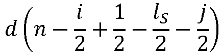
- At the FIR tap rs = 3, the 1-
sample delay device 113c in the subsequent stage of thesub-sample delay filter 111 outputs
- At the FIR tap rs = 4, the 1-
sample delay device 113b in the subsequent stage of the 1-sample delay device 113a outputs
- A generalized expression of the output from each of the aforementioned five taps in the FIRls related to each memory tap ls with the memory tap ls (= 0, 1, or 2) and the FIR tap rs (= 0, 1, 2, 3, or 4) as variables is as follows.

- In other words, the output signal of each FIR tap rs corresponding to delaying in steps of one sample in sampling after the aforementioned twofold interpolation is expressed as follows.

- Each of the
complex multipliers complex multipliers adder 115. The signal added by theadder 115 is output from each of theFIR filter 0 107a, theFIR filter 1 107b, and theFIR filter 2 107c as
- At this time, the output signal of the
FIR filter 0 107a related to the memory tap ls = 0 is as follows.
- The output signal of the
FIR filter 1 107b related to the memory tap ls = 1 is as follows.
- The output signal of the
FIR filter 2 107c related to the memory tap ls = 2 is as follows.
- The output signals of the
FIR filter 0 107a, theFIR filter 1 107b, and theFIR filter 2 107c are eventually added by theadder 108, and the added signal is output from theDPD 1 as a polynomial expressed by the aforementioned equation (20) with a reduced number of coefficients. - As described above, the tap coefficients of the pseudo-interpolation/sub-sample-
shift filters sub-sample delay filter 111 are known fixed coefficients and do not need to be changed. - Further, the i/2-
sample delay device 102 is a fixed delay device determined by the number of taps i of the pseudo-interpolation/sub-sample-shift filters sample delay device 112 is a fixed delay device determined by the number of taps j of thesub-sample delay filter 111. - Accordingly, in the
DPD 1 according toPatent Literature 3 illustrated inFig. 9 , the number of power series coefficients in theLUTs FIR filter 0 107a, theFIR filter 1 107b, and theFIR filter 2 107c that need to be derived and updated by adaptive control are identical to the number of coefficients in the aforementioned equation (8) in which the number of coefficients is reduced by 30% and the configuration illustrated inFig. 5 , in comparison with the related art. - First, for the purpose of comparison, an example of, in a distortion compensation apparatus not performing DPD upsampling, using a signal with a system bandwidth of 800 MHz at a sampling frequency of 983.04 MHz as an input signal of the
DPD 1 without upsampling and operating theDPD 1 by adaptive control with the following equation (22) as an error evaluation function by applying the aforementioned equation (8) and the configuration inFig. 5 is described.
- Note that, in the equation (22), xu(n) and zu(n) in the aforementioned equation (10) are substituted by x(n) and z(n), respectively, based on
Fig. 6 , in order to adapt to the configuration in which DPD upsampling is not performed. - With the aforementioned equation (8) and the configuration in
Fig. 5 , theDPD 1 operating at a sampling rate before interpolation by theinterpolation DA converter 2 in the subsequent stage of theDPD 1 cannot generate a distortion compensation signal compensating for a memory effect within a carrier band for a sub-sample. - On the other hand, a case of using a signal with a system bandwidth of 800 MHz at a sampling frequency of 983.04 MHz as an input signal of the
DPD 1 without upsampling, similarly to the above but operating theDPD 1 by adaptive control with the aforementioned equation (22) as an error evaluation function by applying the aforementioned equation (20) and the configuration inFig. 9 is considered. In this case, as indicated in the description of the aforementioned equation (20) and the configuration inFig. 9 , a distortion compensation signal compensating for a memory effect within the carrier band for a sub-sample for theDPD 1 can be generated by the sub-sample memory taps provided by the pseudo-interpolation/sub-sample-shift filters sub-sample delay filter 111. - As described above, the
DPD 1 according toPatent Literature 3 illustrated inFig. 9 is premised on operation at a low sampling rate for sampling an input signal not DPD upsampled in a previous stage of theDPD 1. - By using a polynomial structure including the pseudo-interpolation/sub-sample-
shift filters DPD 1 according toPatent Literature 3 illustrated inFig. 9 can generate, for example, a signal corresponding to the twofold-upsampled signal xu(n-ls) in the aforementioned equation (8) with a reduced number of coefficients andFig. 5 from a sample signal sequence of non-upsampled input signals of theDPD 1. - Further, by using the
FIR filter 0 107a, theFIR filter 1 107b, and theFIR filter 2 107c each including thesub-sample delay filter 111, the FIR filters being placed in a subsequent stage of the polynomial structure, theDPD 1 according toPatent Literature 3 illustrated inFig. 9 can provide, for example, an FIR filter equivalent to theFIR filter 0 405a, theFIR filter 1 405b, and theFIR filter 2 405c inFig. 5 operating at a twofold sampling frequency. - Therefore, by using the aforementioned polynomial structure, and the
FIR filter 0 107a, theFIR filter 1 107b, and theFIR filter 2 107c, theDPD 1 according toPatent Literature 3 illustrated inFig. 9 not only compensates for distortion due to a sample point but also compensates for distortion due to a sub-sample point between sample points for theDPD 1. - Accordingly, while the distortion compensation apparatus according to
Patent Literature 3 illustrated inFig. 9 is a distortion compensation apparatus operating at a low sampling rate without performing DPD upsampling processing in a previous stage of theDPD 1, the apparatus can reduce an amount of coefficient calculation and can also reduce the operating frequency of theDPD 1 and sampling rates of theDA converter 2 and theAD converter 7, compared with the upsampling distortion compensation apparatus according to the related art. Furthermore, the distortion compensation apparatus can compensate for a memory effect within a carrier band due to a sub-sample memory tap between sample points in theDPD 1 and therefore can achieve target compensation performance. - While the
DPD 1 according toPatent Literature 3 illustrated inFig. 9 has been described above, the technology according toPatent Literature 3 has another problem. - With regard to the polynomial structure according to
Patent Literature 3,Patent Literature 3 mentions an application example of a cross-term configuration in which combinations of complex multiplication of a signal
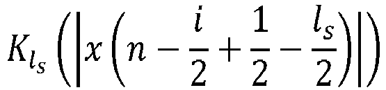
complex multipliers - However, in construction of a power amplifier model optimum for distortion compensation, a complex multiplication configuration based on fixed cross terms has a problem that a degree of freedom does not exist in the configuration, and hardware in which memory taps for each combination of cross terms to be complex-multiplied are changed for each amplifier to be compensated is required.
- On the other hand, when a circuit configuration is generalized in such a way as to support any cross-term combination, there remains another problem that the circuit becomes complex, and the primary purpose of achieving target compensation performance while reducing the number of coefficients cannot be achieved.
- In view of the problems described above, an object of the present disclosure is to provide a distortion compensation apparatus and a distortion compensation method that can give a degree of freedom to a combination in a cross-term-based complex multiplication configuration with a small amount of circuit addition without increasing the number of coefficients.
- In order to solve the aforementioned problems, a distortion compensation apparatus according to the present disclosure is a distortion compensation apparatus configured to compensate for non-linear distortion of a power amplifier and includes:
- an AD converter configured to feed back and analog/digital (AD) convert an output signal of the power amplifier and output the AD converted signal as a feedback signal;
- a digital predistorter configured to perform distortion compensation processing on an input signal by using the feedback signal and output the signal undergoing distortion compensation processing; and
- a DA converter configured to be provided between the digital predistorter and the power amplifier, digital/analog (DA) convert an output signal of the digital predistorter, and output the DA converted signal to the power amplifier,
- wherein the digital predistorter
- operates at a sampling rate for sampling the input signal not upsampled in a previous stage of the digital predistorter,
- includes:
- a polynomial structure configured to include a pseudo-interpolation/sub-sample-shift processing unit configured to pseudo-interpolate a sample point between sample points of the input signal and shift the pseudo-interpolated sample point by a sub-sample and include a multiplexer configured to select a combination of a sub-sample shift amount in complex-multiplication of a signal itself acquired by processing the input signal by the pseudo-interpolation/sub-sample-shift processing unit by an output of a look up table related to an amplitude address corresponding to an amplitude of a signal acquired by processing the input signal by the pseudo-interpolation/sub-sample-shift processing unit; and
- a finite impulse response (FIR) filter configured to be provided in a subsequent stage of the polynomial structure and include a sub-sample delay filter delaying a sample point of the input signal by a sub-sample, and
- compensates for distortion due to a sample point of the input signal and compensates for distortion due to a sub-sample point between sample points of the input signal for the digital predistorter, by using the polynomial structure and the FIR filter.
- In order to solve the aforementioned problems, a distortion compensation method according to the present disclosure is a distortion compensation method by a distortion compensation apparatus configured to compensate for non-linear distortion of a power amplifier and includes:
- in a digital predistorter, performing distortion compensation processing on an input signal by using a feedback signal acquired by feeding back and analog/digital (AD) converting an output signal of the power amplifier, and outputting the signal undergoing distortion compensation processing; and
- digital/analog (DA) converting an output signal of the digital predistorter and outputting the DA converted signal to the power amplifier,
- wherein the digital predistorter
- operates at a sampling rate for sampling the input signal not upsampled in a previous stage of the digital predistorter,
- includes:
- a polynomial structure configured to include a pseudo-interpolation/sub-sample-shift processing unit configured to pseudo-interpolate a sample point between sample points of the input signal and shift the pseudo-interpolated sample point by a sub-sample and include a multiplexer configured to select a combination of a sub-sample shift amount in complex-multiplication of a signal itself acquired by processing the input signal by the pseudo-interpolation/sub-sample-shift processing unit by an output of a look up table related to an amplitude address corresponding to an amplitude of a signal acquired by processing the input signal by the pseudo-interpolation/sub-sample-shift processing unit; and
- a finite impulse response (FIR) filter configured to be provided in a subsequent stage of the polynomial structure and include a sub-sample delay filter delaying a sample point of the input signal by a sub-sample, and
- compensates for distortion due to a sample point of the input signal and compensates for distortion due to a sub-sample point between sample points of the input signal for the digital predistorter, by using the polynomial structure and the FIR filter.
- The present disclosure produces an effect of providing a distortion compensation apparatus and a distortion compensation method that can give a degree of freedom to a combination in a cross-term-based complex-multiplication configuration with a small amount of circuit addition without increasing the number of coefficients.
-
-
Fig. 1A is a block diagram illustrating a configuration example of a DPD according to an example embodiment of the present disclosure. -
Fig. 1B is a block diagram illustrating a configuration example of an FIR filter in the DPD according to the example embodiment of the present disclosure. -
Fig. 2 is a block diagram illustrating a configuration example of a distortion compensation apparatus according to a related art. -
Fig. 3 is a block diagram illustrating a functional example of an interpolation DA converter. -
Fig. 4 is a block diagram illustrating a configuration example of a DPD in the distortion compensation apparatus according to the related art illustrated inFig. 2 . -
Fig. 5 is a block diagram illustrating a configuration example of a DPD acquired by applying a measure for reducing the number of coefficients to the DPD according to the related art illustrated inFig. 4 . -
Fig. 6 is a block diagram illustrating a configuration example of a distortion compensation apparatus in which an interpolation circuit is deleted and DPD upsampling is not performed. -
Fig. 7 is a diagram illustrating a comparison example between amplitude changes of a signal in an 800 MHz bandwidth at a sampling frequency of 983.04 MHz before interpolation and amplitude changes of a signal acquired by twofold-upsampling the signal at a sampling frequency of 1.96608 GHz by twofold interpolation processing. -
Fig. 8 is a diagram illustrating a comparison example between amplitude changes of a signal twofold-upsampled at a sampling frequency of 1.96608 GHz by twofold interpolation processing and amplitude changes of a signal acquired by further fourfold-upsampling the signal at a sampling frequency of 3.93216 GHz by twofold interpolation processing. -
Fig. 9 is a block diagram illustrating a configuration example of a DPD disclosed inPatent Literature 3. -
Fig. 10 is a diagram illustrating an example of tap coefficients of a twofold-interpolation half-band FIR filter incorporated in an interpolation DA converter. -
Fig. 11 is a timing chart illustrating an example of twofold interpolation processing in the interpolation DA converter. -
Fig. 12 is a diagram illustrating an example of a procedure for acquiring tap coefficients of a pseudo-interpolation filter for acquiring sub-sample memory taps = ±0.5 for a DPD operating at a non-upsampled sampling rate. -
Fig. 13A is a diagram illustrating an example of an impulse response of a 0.5-sample delay filter in a case of a delay being a non-integer relative to a sample. -
Fig. 13B is a diagram illustrating an example of a frequency characteristic of an amount of filter attenuation for the number of taps when a 0.5-sample delay filter is configured with an FIR filter. - An example embodiment of the present disclosure is described below with reference to drawings.
-
Fig. 1A andFig. 1B illustrate block diagrams of a configuration example of aDPD 1 according to the present example embodiment.Fig. 1A illustrates a configuration example of theDPD 1 according to the present example embodiment, andFig. 1B illustrates a configuration example of anFIR filter 0 107a, anFIR filter 1 107b, and anFIR filter 2 107c in theDPD 1 according to the present example embodiment. - The
DPD 1 according to the present example embodiment illustrated inFig. 1A andFig. 1B includes amultiplexer 0 109a, amultiplexer 1 109b, and amultiplexer 2 109c in addition to theDPD 1 according toPatent Literature 3 illustrated inFig. 9 . - The
multiplexer 0 109a is a multiplexer that can select a signal to be complex-multiplied by an output of aLUT 105a by acomplex multiplier 106a in a path related to a memory tap ls = 0, that is, a path in which the pseudo-interpolation/sub-sample-shift filter 101a, an amplitudeaddress calculation circuit 104a, and theLUT 105a are placed from among an output of a pseudo-interpolation/sub-sample-shift filter 101a, an output of an i/2-sample delay device 102, and an output of a pseudo-interpolation/sub-sample-shift filter 101b. - The
multiplexer 1 109b is a multiplexer that can select a signal to be complex-multiplied by an output of aLUT 105b by acomplex multiplier 106b in a path related to a memory tap ls = 1, that is, a path in which the i/2-sample delay device 102, an amplitudeaddress calculation circuit 104b, and theLUT 105b are placed from among the output of the pseudo-interpolation/sub-sample-shift filter 101a, the output of the i/2-sample delay device 102, and the output of the pseudo-interpolation/sub-sample-shift filter 101b. - The
multiplexer 2 109c is a multiplexer that can select a signal to be complex-multiplied by an output of aLUT 105c by acomplex multiplier 106c in a path related to a memory tap ls = 2, that is, a path in which the pseudo-interpolation/sub-sample-shift filter 101b, an amplitudeaddress calculation circuit 104c, and theLUT 105c are placed from among the output of the pseudo-interpolation/sub-sample-shift filter 101a, the output of the i/2-sample delay device 102, and the output of the pseudo-interpolation/sub-sample-shift filter 101b. - A multiplexer is generally a circuit mechanism selecting or aggregating two or more inputs and outputting one resulting signal. Each of the multiplexer0 109a, the
multiplexer 1 109b, and themultiplexer 2 109c according to the present disclosure is a multiplexer as a data selector and, for example, includes three lines of data inputs and one line of a data output. Each of the multiplexer0 109a, themultiplexer 1 109b, and themultiplexer 2 109c selects one line from among the three lines of input signals and set the selected one line as an output signal in accordance with each of selection control signals SELo, SEL1, and SEL2. - In a path related to a memory tap ls (ls = 0, 1, or 2), a memory tap of, in sampling after twofold interpolation, a signal selected by a multiplexer for each path from among the output of the pseudo-interpolation/sub-sample-
shift filter 101a, the output of the i/2-sample delay device 102, and the output of the pseudo-interpolation/sub-sample-shift filter 101b, is expressed as mls. - Specifically, the memory tap of a signal output selected by the
multiplexer 0 109a for the path related to ls = 0 is mls = mo. The memory tap of a signal output selected by themultiplexer 1 109b for the path related to ls = 1 is mls = mi. The memory tap of a signal output selected by themultiplexer 2 109c for the path related to ls = 2 is mls = m2. One of 0, 1, and 2 is selected as mls in the example inFig. 1A andFig. 1B . - In the configuration according to the present example embodiment, based on LUT amplitude addresses for signals corresponding to delaying in steps of one sample in sampling after twofold interpolation, the
LUTs LUTs complex multipliers complex multipliers DPD 1 according to the present example embodiment, that is, an output for each term of the memory tap ls in a polynomial structure is as follows.
- The memory tap mls (mls = 0, 1, or 2) in the path related to the memory tap ls (ls = 0, 1, or 2) can be selected by the
multiplexer 0 109a for the path related to ls = 0, themultiplexer 1 109b for the path related to ls = 1, or themultiplexer 2 109c for the path related to ls = 2. - The results of complex-multiplication by the
complex multipliers FIR filter 0 107a, theFIR filter 1 107b, and theFIR filter 2 107c, respectively, as a polynomial
FIR filter 0 107a is related to the memory tap ls = 0 in sampling after twofold interpolation. TheFIR filter 1 107b is related to the memory tap ls = 1 in sampling after twofold interpolation. TheFIR filter 2 107c is related to the memory tap ls = 2 in sampling after twofold interpolation. - From an input signal

FIR filter 0 107a, theFIR filter 1 107b, and theFIR filter 2 107c outputs signals described below related to FIR taps rs = 0, 1, 2, 3, and 4, respectively, in sampling after twofold interpolation. - At the FIR tap rs = 0,

sample delay device 112 in sampling after twofold interpolation is output. - At the FIR tap rs = 1,

sub-sample delay filter 111 configured with a j-tap FIR filter in sampling after twofold interpolation is output. - At the FIR tap rs = 2,

sample delay device 113a in a subsequent stage of the (j/2-1)-sample delay device 112 in sampling after twofold interpolation is output. - At the FIR tap rs = 3,

sample delay device 113c in a subsequent stage of thesub-sample delay filter 111 in sampling after twofold interpolation is output. - At the FIR tap rs = 4,

sample delay device 113b in a subsequent stage of the 1-sample delay device 113a in sampling after twofold interpolation is output. - A generalized expression of the output from each of the aforementioned five taps in the FIRls related to each memory tap ls with the memory tap ls (= 0, 1, or 2) and the FIR tap rs (= 0, 1, 2, 3, or 4) as variables is as follows.

- In other words, the output signal of each FIR tap rs corresponding to delaying in steps of one sample in the aforementioned sampling after twofold interpolation is expressed as follows.

- Each of the
complex multipliers complex multipliers adder 115. The signal added by theadder 115 is output from each of theFIR filter 0 107a, theFIR filter 1 107b, and theFIR filter 2 107c as
- At this time, the output signal of the
FIR filter 0 107a related to the memory tap ls = 0 is as follows.
- The output signal of the
FIR filter 1 107b related to the memory tap ls = 1 is as follows.
- The output signal of the
FIR filter 2 107c related to the, memory tap ls = 2 is as follows.
- The output signals of the
FIR filter 0 107a, theFIR filter 1 107b, and theFIR filter 2 107c are eventually added by anadder 108. The result of the addition by theadder 108 corresponds to the equation (20) in theDPD 1 according toPatent Literature 3 illustrated inFig. 9 and is output from theDPD 1 as a polynomial with a reduced number of coefficients expressed by the following equation (23) in theDPD 1 according to the present example embodiment.
- As described above, the
DPD 1 according to the present example embodiment can freely select a value of a memory tap mls (mls = 0, 1, or 2) being identical to or different from a value of ls for a path related to a memory tap ls (ls = 0, 1, or 2) by a polynomial structure including a multiplexer selecting a combination of sub-sample shift amounts and selection control on the multiplexer. - Accordingly, while being a distortion compensation apparatus not performing DPD upsampling processing in a previous stage of the
DPD 1 and operating at a low sampling rate, the distortion compensation apparatus according to the present example embodiment can reduce an amount of coefficient calculation and can reduce the operating frequency of theDPD 1 and the sampling rates of theDA converter 2 and theAD converter 7, compared with the upsampling distortion compensation apparatus according to the related art. Furthermore, in compensation for a memory effect within a carrier band due to a sub-sample memory tap between sample points in theDPD 1, a degree of freedom can be given to a combination of complex-multiplication configurations based on cross terms with different memory taps (= sub-sample shift amounts) by a polynomial structure including a multiplexer selecting a combination of sub-sample shift amounts and selection control on the multiplexer, without increasing the number of coefficients and with a small amount of circuit addition. Therefore, a power amplifier model optimum for distortion compensation can be constructed, and target compensation performance can be achieved. - While various aspects of the present disclosure have been described above with reference to the example embodiments, the present disclosure is not limited to the aforementioned example embodiments. Various changes and modifications in each aspect of the present disclosure that may be understood by a person skilled in the art may be made to the configurations and details of the present invention within the scope of the present invention.
- For example, the number of memory taps ls and mls, and the number of FIR taps rs indicated in the aforementioned example embodiment are examples and are not restrictive. For example, while the number of memory taps ls and mls are set to 3, and the number of FIR taps rs is set to 5 as an example of approximating a seventh-order memory polynomial model in the aforementioned example embodiment, the seventh-order memory polynomial model may be approximated by setting the number of memory taps ls and mls to 5 and the number of FIR taps rs to 3. Further, permitting increase in the circuit size and the amount of coefficient calculation, the aforementioned number of taps may be increased.
- This application claims priority based on
Japanese Patent Application No. 2020-083960 filed on May 12, 2020 -
- 1 DIGITAL PREDISTORTER (DPD)
- 2 DIGITAL/ANALOG (DA) CONVERTER
- 3 TRANSMISSION UPCONVERTER
- 4 POWER AMPLIFIER
- 5 DIRECTIONAL COUPLER
- 6 FEEDBACK DOWNCONVERTER
- 7 ANALOG/DIGITAL (AD) CONVERTER
- 101a, 101b PSEUDO-INTERPOLATION/SUB-SAMPLE-SHIFT FILTER
- 102 i/2-SAMPLE DELAY DEVICE
- 103 1-SAMPLE DELAY DEVICE
- 104a, 104b, 104c AMPLITUDE ADDRESS CALCULATION CIRCUIT
- 105a, 105b, 105c LOOK UP TABLE (LUT)
- 106a, 106b, 106c COMPLEX MULTIPLIER
- 107a FIR FILTER0
- 107b FIR FILTER1
- 107c FIR FILTER2
- 108 ADDER
- 109a MULTIPLEXER0
- 109b MULTIPLEXER1
- 109c MULTIPLEXER2
- 111 SUB-SAMPLE DELAY FILTER
- 112 (j/2-1)-SAMPLE DELAY DEVICE
- 113a, 113b, 113c 1-SAMPLE DELAY DEVICE
- 114a, 114b, 114c, 114d, 114e COMPLEX MULTIPLIER
- 115 ADDER
- 201, 202 HALF-BAND FILTER1
- 203, 204 HALF-BAND FILTER2
- 205 NUMERICAL CONTROLLED OSCILLATOR (NCO)
- 206, 207 COMPLEX MULTIPLIER
- 208 ADDER
- 209 DA CONVERSION UNIT
Claims (6)
- A distortion compensation apparatus configured to compensate for non-linear distortion of a power amplifier, the distortion compensation apparatus comprising:an AD converter configured to feed back and analog/digital (AD) convert an output signal of the power amplifier and output the AD converted signal as a feedback signal;a digital predistorter configured to perform distortion compensation processing on an input signal by using the feedback signal and output the signal undergoing distortion compensation processing; anda DA converter configured to be provided between the digital predistorter and the power amplifier, digital/analog (DA) convert an output signal of the digital predistorter, and output the DA converted signal to the power amplifier,wherein the digital predistorteroperates at a sampling rate for sampling the input signal not upsampled in a previous stage of the digital predistorter,includes:a polynomial structure configured to include a pseudo-interpolation/sub-sample-shift processing unit configured to pseudo-interpolate a sample point between sample points of the input signal and shift the pseudo-interpolated sample point by a sub-sample and include a multiplexer configured to select a combination of a sub-sample shift amount in complex-multiplication of a signal itself acquired by processing the input signal by the pseudo-interpolation/sub-sample-shift processing unit by an output of a look up table related to an amplitude address corresponding to an amplitude of a signal acquired by processing the input signal by the pseudo-interpolation/sub-sample-shift processing unit; anda finite impulse response (FIR) filter configured to be provided in a subsequent stage of the polynomial structure and include a sub-sample delay filter delaying a sample point of the input signal by a sub-sample, andcompensates for distortion due to a sample point of the input signal and compensates for distortion due to a sub-sample point between sample points of the input signal for the digital predistorter, by using the polynomial structure and the FIR filter.
- The distortion compensation apparatus according to Claim 1, wherein the digital predistorterincludes:a plurality of the FIR filters; anda first adder configured to add and output respective output signals of a plurality of the FIR filters andhas a configuration in which a plurality of first paths of the polynomial structure are branched in parallel from an input stage of the digital predistorter, a plurality of the FIR filters are placed in a subsequent stage of a plurality of the first path, respectively, and the first adder is placed in a subsequent stage of a plurality of the FIR filters, andthe pseudo-interpolation/sub-sample-shift processing unit is placed in the first path.
- The distortion compensation apparatus according to Claim 2, wherein a plurality of the first paths include:the first path in which the pseudo-interpolation/sub-sample-shift processing unit is placed; andthe first path in which the pseudo-interpolation/sub-sample-shift processing unit is not placed.
- The distortion compensation apparatus according to Claim 3, whereinthe pseudo-interpolation/sub-sample-shift processing unit is a filter with a fixed tap coefficient, anda first delay device with an amount of delay determined by the number of taps of the pseudo-interpolation/sub-sample-shift processing unit is placed in the first path in which the pseudo-interpolation/sub-sample-shift processing unit is not placed.
- The distortion compensation apparatus according to Claim 4, wherein the multiplexer selects a signal to be complex-multiplied by an output of the look up table from either of an output of the pseudo-interpolation/sub-sample-shift processing unit in a plurality of the first paths and an output of the first delay device.
- A distortion compensation method by a distortion compensation apparatus configured to compensate for non-linear distortion of a power amplifier, the distortion compensation method comprising:in a digital predistorter, performing distortion compensation processing on an input signal by using a feedback signal acquired by feeding back and analog/digital (AD) converting an output signal of the power amplifier, and outputting the signal undergoing distortion compensation processing; anddigital/analog (DA) converting an output signal of the digital predistorter and outputting the DA converted signal to the power amplifier,wherein the digital predistorteroperates at a sampling rate for sampling the input signal not upsampled in a previous stage of the digital predistorter,includes:a polynomial structure configured to include a pseudo-interpolation/sub-sample-shift processing unit configured to pseudo-interpolate a sample point between sample points of the input signal and shift the pseudo-interpolated sample point by a sub-sample and include a multiplexer configured to select a combination of a sub-sample shift amount in complex-multiplication of a signal itself acquired by processing the input signal by the pseudo-interpolation/sub-sample-shift processing unit by an output of a look up table related to an amplitude address corresponding to an amplitude of a signal acquired by processing the input signal by the pseudo-interpolation/sub-sample-shift processing unit; anda finite impulse response (FIR) filter configured to be provided in a subsequent stage of the polynomial structure and include a sub-sample delay filter delaying a sample point of the input signal by a sub-sample, andcompensates for distortion due to a sample point of the input signal and compensates for distortion due to a sub-sample point between sample points of the input signal for the digital predistorter, by using the polynomial structure and the FIR filter.
Applications Claiming Priority (2)
| Application Number | Priority Date | Filing Date | Title |
|---|---|---|---|
| JP2020083960 | 2020-05-12 | ||
| PCT/JP2021/011096 WO2021229913A1 (en) | 2020-05-12 | 2021-03-18 | Distortion compensation device and distortion compensation method |
Publications (2)
| Publication Number | Publication Date |
|---|---|
| EP4007164A1 true EP4007164A1 (en) | 2022-06-01 |
| EP4007164A4 EP4007164A4 (en) | 2022-11-23 |
Family
ID=78525709
Family Applications (1)
| Application Number | Title | Priority Date | Filing Date |
|---|---|---|---|
| EP21805228.0A Withdrawn EP4007164A4 (en) | 2020-05-12 | 2021-03-18 | Distortion compensation device and distortion compensation method |
Country Status (4)
| Country | Link |
|---|---|
| US (1) | US11777543B2 (en) |
| EP (1) | EP4007164A4 (en) |
| JP (1) | JP7364062B2 (en) |
| WO (1) | WO2021229913A1 (en) |
Families Citing this family (1)
| Publication number | Priority date | Publication date | Assignee | Title |
|---|---|---|---|---|
| FI20225668A1 (en) * | 2022-07-14 | 2024-01-15 | Nokia Solutions & Networks Oy | Predistortion method |
Family Cites Families (8)
| Publication number | Priority date | Publication date | Assignee | Title |
|---|---|---|---|---|
| GB2376584B (en) * | 2001-06-15 | 2005-02-16 | Wireless Systems Int Ltd | Signal correction techniques |
| US8537041B2 (en) | 2011-05-12 | 2013-09-17 | Andrew Llc | Interpolation-based digital pre-distortion architecture |
| CN102893399B (en) | 2012-05-24 | 2015-09-09 | 华为技术有限公司 | Predistortion correction method, predistortion correction device, transmitter and base station |
| PT3528787T (en) | 2016-10-21 | 2026-03-11 | Amgen Inc | Pharmaceutical formulations and methods for producing them. |
| US11005430B2 (en) | 2017-03-02 | 2021-05-11 | Sumitomo Electric Industries, Ltd. | Distortion compensation device and distortion compensation method |
| CN107895074A (en) | 2017-11-08 | 2018-04-10 | 重庆工程职业技术学院 | A kind of mixing double frequency digital pre-distortion model method based on DDR |
| JP7024420B2 (en) | 2018-01-12 | 2022-02-24 | 日本電気株式会社 | Strain compensation device and strain compensation method |
| JP2020083960A (en) | 2018-11-20 | 2020-06-04 | Nok株式会社 | Anisotropic conductive adhesive and current cut-off device |
-
2021
- 2021-03-18 EP EP21805228.0A patent/EP4007164A4/en not_active Withdrawn
- 2021-03-18 JP JP2022522535A patent/JP7364062B2/en active Active
- 2021-03-18 US US17/636,457 patent/US11777543B2/en active Active
- 2021-03-18 WO PCT/JP2021/011096 patent/WO2021229913A1/en not_active Ceased
Also Published As
| Publication number | Publication date |
|---|---|
| WO2021229913A1 (en) | 2021-11-18 |
| EP4007164A4 (en) | 2022-11-23 |
| US20220311462A1 (en) | 2022-09-29 |
| JP7364062B2 (en) | 2023-10-18 |
| US11777543B2 (en) | 2023-10-03 |
| JPWO2021229913A1 (en) | 2021-11-18 |
Similar Documents
| Publication | Publication Date | Title |
|---|---|---|
| JP7024420B2 (en) | Strain compensation device and strain compensation method | |
| US11245429B2 (en) | System and method for increasing bandwidth for digital predistortion in multi-channel wideband communication systems | |
| US10218392B2 (en) | Wide bandwidth digital predistortion system with reduced sampling rate | |
| US6298097B1 (en) | Amplifier with wideband digital predistortion | |
| CN103188199B (en) | A kind of broadband despicking method and device based on fraction delay CPG | |
| US11563409B2 (en) | Configurable non-linear filter for digital pre-distortion | |
| US9385764B2 (en) | Digital pre-distortion for high bandwidth signals | |
| CN111436225A (en) | Predistortion circuit, method for generating a predistorted baseband signal, control circuit for a predistortion circuit, method for determining parameters of a predistortion circuit, and apparatus and method for predistorting a baseband signal | |
| WO2001039367A1 (en) | Method and apparatus for generating a radio frequency signal | |
| US7570707B2 (en) | Digital delay element for delay mismatch cancellation in wireless polar transmitters | |
| US11757475B2 (en) | Low-complexity inverse sinc for RF sampling transmitters | |
| EP4007164A1 (en) | Distortion compensation device and distortion compensation method | |
| JP5731325B2 (en) | Modulator and amplifier using the same | |
| TWI854750B (en) | Digital pre-distortion circuit and method for generating a digital pre-distortion signal | |
| Jaraut et al. | Complexity and numerical stability investigation in concurrent dual-band modeling of ultra-wideband power amplifiers for harmonically related signals | |
| Chen et al. | Broadband doherty power amplifier and linearization | |
| CN119448948A (en) | Digital predistortion circuit and method for generating predistortion signal | |
| EP2040375A1 (en) | Power amplifier module and method of generating a drain voltage for a power amplifier | |
| Murillo-Fuentes et al. | Applying GCMAC to predistortion in GSM base stations | |
| Abdelnaby | Behavioral Modeling of RF Power Amplifiers Using Reduced Sampling Rate | |
| SI23781A (en) | Device for compensation of non-linearity broadband amplifier | |
| HK1195829A (en) | System and method for increasing bandwidth for digital predistortion in multi-channel wideband communication systems |
Legal Events
| Date | Code | Title | Description |
|---|---|---|---|
| STAA | Information on the status of an ep patent application or granted ep patent |
Free format text: STATUS: THE INTERNATIONAL PUBLICATION HAS BEEN MADE |
|
| PUAI | Public reference made under article 153(3) epc to a published international application that has entered the european phase |
Free format text: ORIGINAL CODE: 0009012 |
|
| STAA | Information on the status of an ep patent application or granted ep patent |
Free format text: STATUS: REQUEST FOR EXAMINATION WAS MADE |
|
| 17P | Request for examination filed |
Effective date: 20220225 |
|
| AK | Designated contracting states |
Kind code of ref document: A1 Designated state(s): AL AT BE BG CH CY CZ DE DK EE ES FI FR GB GR HR HU IE IS IT LI LT LU LV MC MK MT NL NO PL PT RO RS SE SI SK SM TR |
|
| STAA | Information on the status of an ep patent application or granted ep patent |
Free format text: STATUS: THE APPLICATION HAS BEEN WITHDRAWN |
|
| A4 | Supplementary search report drawn up and despatched |
Effective date: 20221021 |
|
| RIC1 | Information provided on ipc code assigned before grant |
Ipc: H03F 3/24 20060101ALI20221017BHEP Ipc: H03F 3/189 20060101ALI20221017BHEP Ipc: H03F 1/32 20060101AFI20221017BHEP |
|
| 18W | Application withdrawn |
Effective date: 20221101 |