EP4006964A1 - Electronic device - Google Patents
Electronic device Download PDFInfo
- Publication number
- EP4006964A1 EP4006964A1 EP21207688.9A EP21207688A EP4006964A1 EP 4006964 A1 EP4006964 A1 EP 4006964A1 EP 21207688 A EP21207688 A EP 21207688A EP 4006964 A1 EP4006964 A1 EP 4006964A1
- Authority
- EP
- European Patent Office
- Prior art keywords
- semiconductor layer
- electronic device
- layer
- disposed
- transistor
- Prior art date
- Legal status (The legal status is an assumption and is not a legal conclusion. Google has not performed a legal analysis and makes no representation as to the accuracy of the status listed.)
- Pending
Links
Images


Classifications
-
- H—ELECTRICITY
- H10—SEMICONDUCTOR DEVICES; ELECTRIC SOLID-STATE DEVICES NOT OTHERWISE PROVIDED FOR
- H10D—INORGANIC ELECTRIC SEMICONDUCTOR DEVICES
- H10D84/00—Integrated devices formed in or on semiconductor substrates that comprise only semiconducting layers, e.g. on Si wafers or on GaAs-on-Si wafers
- H10D84/01—Manufacture or treatment
-
- H—ELECTRICITY
- H10—SEMICONDUCTOR DEVICES; ELECTRIC SOLID-STATE DEVICES NOT OTHERWISE PROVIDED FOR
- H10D—INORGANIC ELECTRIC SEMICONDUCTOR DEVICES
- H10D84/00—Integrated devices formed in or on semiconductor substrates that comprise only semiconducting layers, e.g. on Si wafers or on GaAs-on-Si wafers
- H10D84/01—Manufacture or treatment
- H10D84/02—Manufacture or treatment characterised by using material-based technologies
- H10D84/05—Manufacture or treatment characterised by using material-based technologies using Group III-V technology
-
- H—ELECTRICITY
- H10—SEMICONDUCTOR DEVICES; ELECTRIC SOLID-STATE DEVICES NOT OTHERWISE PROVIDED FOR
- H10D—INORGANIC ELECTRIC SEMICONDUCTOR DEVICES
- H10D1/00—Resistors, capacitors or inductors
- H10D1/60—Capacitors
- H10D1/62—Capacitors having potential barriers
- H10D1/64—Variable-capacitance diodes, e.g. varactors
-
- H—ELECTRICITY
- H10—SEMICONDUCTOR DEVICES; ELECTRIC SOLID-STATE DEVICES NOT OTHERWISE PROVIDED FOR
- H10D—INORGANIC ELECTRIC SEMICONDUCTOR DEVICES
- H10D30/00—Field-effect transistors [FET]
- H10D30/40—FETs having zero-dimensional [0D], one-dimensional [1D] or two-dimensional [2D] charge carrier gas channels
- H10D30/47—FETs having zero-dimensional [0D], one-dimensional [1D] or two-dimensional [2D] charge carrier gas channels having two-dimensional [2D] charge carrier gas channels, e.g. nanoribbon FETs or high electron mobility transistors [HEMT]
- H10D30/471—High electron mobility transistors [HEMT] or high hole mobility transistors [HHMT]
- H10D30/475—High electron mobility transistors [HEMT] or high hole mobility transistors [HHMT] having wider bandgap layer formed on top of lower bandgap active layer, e.g. undoped barrier HEMTs such as i-AlGaN/GaN HEMTs
-
- H—ELECTRICITY
- H10—SEMICONDUCTOR DEVICES; ELECTRIC SOLID-STATE DEVICES NOT OTHERWISE PROVIDED FOR
- H10D—INORGANIC ELECTRIC SEMICONDUCTOR DEVICES
- H10D84/00—Integrated devices formed in or on semiconductor substrates that comprise only semiconducting layers, e.g. on Si wafers or on GaAs-on-Si wafers
- H10D84/01—Manufacture or treatment
- H10D84/0123—Integrating together multiple components covered by H10D12/00 or H10D30/00, e.g. integrating multiple IGBTs
-
- H—ELECTRICITY
- H10—SEMICONDUCTOR DEVICES; ELECTRIC SOLID-STATE DEVICES NOT OTHERWISE PROVIDED FOR
- H10D—INORGANIC ELECTRIC SEMICONDUCTOR DEVICES
- H10D84/00—Integrated devices formed in or on semiconductor substrates that comprise only semiconducting layers, e.g. on Si wafers or on GaAs-on-Si wafers
- H10D84/80—Integrated devices formed in or on semiconductor substrates that comprise only semiconducting layers, e.g. on Si wafers or on GaAs-on-Si wafers characterised by the integration of at least one component covered by groups H10D12/00 or H10D30/00, e.g. integration of IGFETs
- H10D84/811—Combinations of field-effect devices and one or more diodes, capacitors or resistors
- H10D84/813—Combinations of field-effect devices and capacitor only
-
- H—ELECTRICITY
- H10—SEMICONDUCTOR DEVICES; ELECTRIC SOLID-STATE DEVICES NOT OTHERWISE PROVIDED FOR
- H10D—INORGANIC ELECTRIC SEMICONDUCTOR DEVICES
- H10D84/00—Integrated devices formed in or on semiconductor substrates that comprise only semiconducting layers, e.g. on Si wafers or on GaAs-on-Si wafers
- H10D84/60—Integrated devices formed in or on semiconductor substrates that comprise only semiconducting layers, e.g. on Si wafers or on GaAs-on-Si wafers characterised by the integration of at least one component covered by groups H10D10/00 or H10D18/00, e.g. integration of BJTs
- H10D84/611—Combinations of BJTs and one or more of diodes, resistors or capacitors
- H10D84/613—Combinations of vertical BJTs and one or more of diodes, resistors or capacitors
- H10D84/615—Combinations of vertical BJTs and one or more of resistors or capacitors
Definitions
- the disclosure relates to an electronic device, and more particularly, to an electronic device that may simplify manufacturing process, reduce costs, or reduce dimensions.
- Electronic devices or tiling electronic devices have been widely used in mobile phones, televisions, monitors, tablet computers, car displays, wearable devices, and desktop computers. With the vigorous development of electronic devices, the quality requirements for electronic devices is higher.
- the disclosure provides an electronic device having the effects of simplifying manufacturing process, reducing costs, or reducing dimensions.
- an electronic device includes a substrate, a transistor, and a variable capacitor.
- the transistor is disposed on the substrate.
- the variable capacitor is disposed on the substrate and adjacent to the transistor.
- a material of the transistor and a material of the variable capacitor both include a III-V semiconductor material.
- first, second, third... may be used to describe various constituent elements, the constituent elements are not limited to these terms. These terms are used to distinguish a single constituent element from other constituent elements in the specification. The same terms may not be used in the claims, and the elements in the claims may be replaced with first, second, third...according to the order stated by the elements in the claims. Therefore, in the following description, the first constituent element may be the second constituent element in the claims.
- connection may mean that two structures are in direct contact, or that two structures are not in direct contact and there are other structures located between these two structures.
- bonding and connecting may also include a case where both structures are movable or both structures are fixed.
- coupled includes any direct and indirect electrical connection means.
- An electronic device of the disclosure may include a display device, an antenna device, a sensing device, a light-emitting device, a touch device, or a tiling device, but is not limited thereto.
- the electronic device may include a bendable or flexible electronic device.
- the appearance of the electronic device may be rectangular, circular, polygonal, a shape with a curved edge, or other suitable shapes.
- the display device may, for example, include a light-emitting diode (LED), liquid crystal, fluorescence, phosphor, quantum dot (QD), other suitable materials, or a combination of the above, but is not limited thereto.
- the LED may include, for example, an organic LED (OLED), inorganic light-emitting diode, mini LED, micro LED, or quantum dot (QD) LED (QLED, QDLED), other suitable materials, or any combination of the above, but is not limited thereto.
- the display device may also include, for example, a tiling display device, but is not limited thereto.
- the antenna device may be, for example, an antenna, but is not limited thereto.
- the antenna device may include, for example, an antenna tiling device, but is not limited thereto. It should be noted that the electronic device may be any combination of the above, but is not limited thereto.
- the appearance of the electronic device may be rectangular, circular, polygonal, a shape with a curved edge, or other suitable shapes.
- the electronic device may have a peripheral system such as a driving system, a control system, a light source system, a shelf system, etc., to support a display device, an antenna device, or a tiling device.
- a peripheral system such as a driving system, a control system, a light source system, a shelf system, etc., to support a display device, an antenna device, or a tiling device.
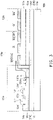
- FIG. 1A is a schematic cross-sectional view of an electronic device of an embodiment of the disclosure.
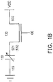
- FIG. 1B is a schematic circuit diagram of the electronic device of FIG. 1A .
- an electronic device 100 of the present embodiment may include a substrate 110, a transistor 120, and a variable capacitor 130.
- the transistor 120 is disposed on the substrate 110.
- the variable capacitor 130 is disposed on the substrate 110, and the variable capacitor 130 is adjacent to the transistor 120.
- the variable capacitor 130 and the transistor 120 are disposed on the same substrate 110.
- there is no other active element or passive element between the variable capacitor 130 and the transistor 120 but the disclosure is not limited thereto.
- the material of the transistor 120 and the material of the variable capacitor 130 both include a III-V semiconductor material.
- the III-V semiconductor material is, for example, gallium arsenide (GaAs), indium arsenide (InAs), aluminum arsenide (AlAs), indium gallium arsenide (InGaAs), aluminum gallium arsenide (AlGaAs), indium aluminum gallium arsenide (InAlGaAs), aluminum nitride (AlN), gallium nitride (GaN), aluminum gallium nitride (AlGaN), indium gallium nitride (InGaN), aluminum indium nitride (AlInN), aluminum indium gallium nitride (AlGaInN), the above materials doped with an N-type dopant, the above materials doped with a P-type dopant, or a combination of the above, but is not limited thereto.
- GaAs gallium arsenide
- InAs aluminum arsenide
- AlAs indium gallium ars
- the substrate 110 may include a rigid substrate, a flexible substrate, or a combination of the above.
- the material of the substrate 110 may include glass, quartz, sapphire, a semiconductor containing an arsenic compound (such as gallium arsenide, but not limited to), ceramic, polycarbonate (PC), polyimide (PI), polyethylene terephthalate (PET), other suitable substrate materials, or a combination of the above, but is not limited thereto.
- the material of the substrate 110 is, for example, a semiconductor containing gallium arsenide, but is not limited thereto.
- the transistor 120 may be a high electron mobility transistor (HEMT) or a heterojunction bipolar transistor (HBT), but is not limited thereto.
- HEMT high electron mobility transistor
- HBT heterojunction bipolar transistor
- the transistor 120 includes a buffer layer 121, a first semiconductor material layer 122, a second semiconductor material layer 123, a heavily-doped semiconductor layer 124 (including a first region 1241 and a second region 1242), a gate GE, a source SD1, and a drain SD2.
- the manufacturing method of the buffer layer 121, the first semiconductor material layer 122, the second semiconductor material layer 123, and the heavily-doped semiconductor layer 124 for example, is first manufacturing by an epitaxy process, and then patterning by lithography etching.
- the method of the epitaxy process is, for example, metal-organic chemical vapor deposition (MOCVD), but is not limited thereto.
- the buffer layer 121 is disposed on the substrate 110.
- the material of the buffer layer 121 includes a III-V semiconductor material.
- the material of the buffer layer 121 is gallium arsenide, but is not limited thereto.
- the first semiconductor material layer 122 is disposed on the buffer layer 121.
- the first semiconductor material layer 122 and the substrate 110 are respectively located at opposite sides of the buffer layer 121.
- the material of the first semiconductor material layer 122 includes a III-V semiconductor material.
- the material of the first semiconductor material layer 122 is aluminum gallium arsenide, but is not limited thereto.
- the heterojunction between the first semiconductor material layer 122 and the buffer layer 121 may have a two-dimensional electron gas (2DEG) 125.
- the second semiconductor material layer 123 is disposed on the first semiconductor material layer 122.
- the second semiconductor material layer 123 and the buffer layer 121 are respectively located at two opposite sides of the first semiconductor material layer 122.
- the material of the second-type semiconductor material layer 123 includes a III-V semiconductor material doped with an N-type dopant or a III-V semiconductor material doped with a P-type dopant.
- the material of the second-type semiconductor material layer 123 is N-type aluminum gallium arsenide, but is not limited thereto.
- the heavily-doped semiconductor layer 124 includes the first region 1241 and the second region 1242.
- the first region 1241 and the second region 1242 of the heavily-doped semiconductor layer 124 are respectively disposed on the second semiconductor material layer 123.
- the first region 1241 and the second region 1242 of the heavily-doped semiconductor layer 124 are physically separated from each other.
- the heavily-doped semiconductor layer 124 and the first semiconductor material layer 122 are respectively located at two opposite sides of the second semiconductor material layer 123.
- the material of the heavily-doped semiconductor layer 124 includes a III-V semiconductor material doped with an N-type dopant or a III-V semiconductor material doped with a P-type dopant.
- the material of the heavily-doped semiconductor layer 124 is N-type gallium arsenide, but is not limited thereto.
- the gate GE is disposed on the second semiconductor material layer 123.
- the gate GE is in contact with the second semiconductor material layer 123.
- the gate GE and the first semiconductor material layer 122 are respectively located at two opposite sides of the second semiconductor material layer 123.
- the gate GE is located between the first region 1241 and the second region 1242 of the heavily-doped semiconductor layer 124.
- the material of the gate GE includes gold, platinum, silver, titanium, chromium, palladium, nickel, other suitable metal materials, or an alloy or combination of the above materials, but is not limited thereto.
- the source SD1 and the drain SD2 are respectively disposed on the first region 1241 and the second region 1242 of the heavily-doped semiconductor layer 124.
- the source SD1 and the second semiconductor material layer 123 are respectively located at two opposite sides of the first region 1241 of the heavily-doped semiconductor layer 124.
- the drain SD2 and the second semiconductor material layer 123 are respectively located at two opposite sides of the second region 1242 of the heavily-doped semiconductor layer 124.
- An ohmic contact may be formed between the source SD1 and the first region 1241 of the heavily-doped semiconductor layer 124, and an ohmic contact may be formed between the drain SD2 and the second region 1242 of the heavily-doped semiconductor layer 124.
- the material of the source SD1 and the drain SD2 includes gold, platinum, silver, titanium, chromium, palladium, nickel, other metal materials that may form an ohmic contact with the heavily-doped semiconductor layer 124, or an alloy or combination of the above materials, but is not limited thereto.
- variable capacitor 130 may be a variable capacitance diode (varactor), but is not limited thereto.
- the variable capacitor 130 includes the first region 1241 of the heavily-doped semiconductor layer 124, a lightly-doped semiconductor layer 131, a first electrode 132, and a second electrode 133.
- the manufacturing method of the lightly-doped semiconductor layer 131 is, for example, first manufacturing using an epitaxy process, and then patterning by lithography etching.
- the method of the epitaxy process is, for example, metal-organic chemical vapor deposition (MOCVD), but is not limited thereto.
- the first region 1241 of the heavily-doped semiconductor layer 124 is disposed on the substrate 110.
- the lightly-doped semiconductor layer 131 is disposed on the first region 1241 of the heavily-doped semiconductor layer 124.
- the lightly-doped semiconductor layer 131 and the second semiconductor material layer 123 are respectively located at two opposite sides of the first region 1241 of the heavily-doped semiconductor layer 124.
- the material of the lightly-doped semiconductor layer 131 includes a III-V semiconductor material doped with an N-type dopant or a III-V semiconductor material doped with a P-type dopant.
- the material of the lightly-doped semiconductor layer 131 is N-type gallium arsenide, but is not limited thereto.
- the doping concentration of the dopant in the lightly-doped semiconductor layer 131 is less than the doping concentration of the dopant in the heavily-doped semiconductor layer 124.
- the first electrode 132 is disposed on the first region 1241 of the heavily-doped semiconductor layer 124, and the first electrode 132 may be electrically connected to the first region 1241 of the heavily-doped semiconductor layer 124.
- the source SD1 of the transistor 120 may be regarded as the first electrode 132 of the variable capacitor 130. That is, the source SD1 of the transistor 120 and the first electrode 132 of the variable capacitor 130 may share the same metal electrode, but is not limited thereto.
- the material of the first electrode 132 is the same as the material of the source electrode SD1, and therefore is not repeated herein.
- the second electrode 133 is disposed on the lightly-doped semiconductor layer 131.
- the junction between the second electrode 133 and the lightly-doped semiconductor layer 131 may have a depletion region 134, and the variable capacitor 130 may also serve as a Schottky diode.
- the material of the second electrode 133 includes gold, platinum, silver, titanium, chromium, palladium, nickel, other metal materials that may form a Schottky contact with the lightly-doped semiconductor layer 131, or an alloy or combination of the above materials, but is not limited thereto.
- the transistor 120 may be electrically connected to the variable capacitor 130, the transistor 120 may be used as a switching element and have a switch function, and the variable capacitor 130 may be used as a capacitive storage element and have the function of adjusting capacitance.
- the voltage of the gate GE may be used to adjust the position of the Fermi level and control the electron concentration of the two-dimensional electron gas 125, so that the transistor 120 is turned on or off.
- a high voltage signal VCC provided to the drain SD2 of the transistor 120 may be transmitted to the source SD1 and the first electrode 132 via a channel formed by the two-dimensional electron gas 125; then, the signal is transferred to the lightly-doped semiconductor layer 131 of the variable capacitor 130 via the first region 1241 of the heavily-doped semiconductor layer 124; then, since the depletion region 134 may be formed at the junction between the second electrode 133 that is grounded (or connected to a low voltage signal) and the lightly-doped semiconductor layer 131, the variable capacitor 130 may store capacitance.
- the storage capacity of the variable capacitor 130 may be changed by adjusting the size of the depletion region 134.
- the depletion region 134 is smaller, and the storable capacitance of the variable capacitor 130 is smaller; conversely, when a reverse bias is provided to the lightly-doped semiconductor layer 131 of the variable capacitor 130, the depletion region 134 is larger, and the storable capacitance of the variable capacitor 130 is larger.
- the material of the transistor 120 and the material of the variable capacitor 130 in the electronic device 100 both include a III-V semiconductor material, and both the transistor 120 and the variable capacitor 130 may be manufactured by an epitaxy process with lithography etching, in the present embodiment, the transistor 120 and the variable capacitor 130 may be formed on the same substrate 110 together, and then the transistor 120 and the variable capacitor 130 are integrated on the same substrate 110.
- a process using a III-V semiconductor material may also reduce manufacturing costs.
- the source SD1 of the transistor 120 and the first electrode 132 of the variable capacitor 130 may share the same metal electrode, there is no need to additionally provide another metal electrode and a pad bonded with the other metal electrode.
- the transistor 120 since the transistor 120 may be electrically connected to the variable capacitor 130, and the transistor 120 and the variable capacitor 130 may share the same metal electrode (i.e., the second electrode 133) that is grounded (or connected to a low voltage signal), it may not be necessary to additionally provide another metal electrode that is grounded (or connected to a low voltage signal) and a pad bonded with the other metal electrode that is grounded (or connected to a low voltage signal).
- the transistor 120 and the variable capacitor 130 may be integrated on the same substrate 110 and share the same metal electrode (i.e., the source SD1 and the first electrode 132) and the same metal electrode that is grounded (or connected to a low voltage signal) (i.e., the second electrode 133), the number of metal electrodes and corresponding pads may be reduced or space may be saved, so that the electronic device 100 of the present embodiment has the effect of simplifying manufacturing process, reducing costs, or reducing dimensions.
- FIG. 2 is a schematic cross-sectional view of an electronic device of another embodiment of the disclosure. Please refer to FIG. 1A and FIG. 2 at the same time.
- An electronic device 100a of the present embodiment is substantially similar to the electronic device 100 of FIG. 1A . Therefore, the same and similar members in the two embodiments are not repeated herein.
- the electronic device 100a of the present embodiment is different from the electronic device 100 mainly in that, in the electronic device 100a of the present embodiment, a variable capacitor 130a does not have a Schottky contact, nor is it a Schottky diode.
- the variable capacitor 130a includes a first-type semiconductor layer 135, a first part 1361 of a second-type semiconductor layer 136, a first-type pad 132a, a second-type pad 133a, and an insulating layer 137.
- the first-type semiconductor layer 135 is disposed on a substrate 110a.
- the material of the first-type semiconductor layer 135 includes a III-V semiconductor material.
- the material of the first-type semiconductor layer 135 is, for example, N-type gallium nitride, but is not limited thereto.
- the second-type semiconductor layer 136 includes the first part 1361 and a second part 1362.
- the first part 1361 and the second part 1362 of the second-type semiconductor layer 136 are physically separated from each other.
- the first part 1361 of the second-type semiconductor layer 136 is disposed on the first-type semiconductor layer 135.
- the first part 1361 of the second-type semiconductor layer 136 and the substrate 110a are respectively located at two opposite sides of the first-type semiconductor layer 135.
- the material of the second-type semiconductor layer 136 includes a III-V semiconductor material.
- the material of the second-type semiconductor layer 136 is, for example, P-type gallium nitride, but is not limited thereto.
- the junction between the first-type semiconductor layer 135 and the first part 1361 of the second-type semiconductor layer 136 may have a depletion region 134a.
- the material of the substrate 110a is, for example, sapphire, but is not limited thereto.
- the first-type pad 132a is disposed on the first-type semiconductor layer 135, and the first-type pad 132a may be electrically connected to the first-type semiconductor layer 135.
- the first-type pad 132a is disposed between the first part 1361 and the second part 1362 of the second-type semiconductor layer 136.
- the first-type pad 132a is in contact with the first-type semiconductor layer 135, and the first-type pad 132a is not in contact with the second-type semiconductor layer 136.
- the second-type pad 133a is disposed on the first part 1361 of the second-type semiconductor layer 136, and the second-type pad 133a may be electrically connected to the first part 1361 of the second-type semiconductor layer 136.
- the conductivity type of the first-type pad 132a is different from the conductivity type of the second-type pad 133a.
- the material of the first-type pad 132a and the second-type pad 133a may include silver, copper, aluminum, molybdenum, tungsten, gold, chromium, nickel, platinum, titanium, iridium, rhodium, indium, bismuth, other suitable metals, or an alloy or combination of the above materials, but is not limited thereto.
- the insulating layer 137 is disposed on the second-type pad 133a, the insulating layer 137 may be extended along a side surface 133al at two sides of the second-type pad 133a and an upper surface 1361a of the first part 1361 and cover part of the upper surface 1361a of the first part 1361, and the insulating layer 137 may also be extended along a side surface 1361b of the first part 1361 and be filled in a gap G between the first part 1361 and the first-type pad 132a.
- the insulating layer 137 has an opening 1371 to expose part of the second-type pad 133a.
- the insulating layer 137 may have a single-layer or multi-layer structure, and may include, for example, an organic material, an inorganic material (such as silicon nitride), or a combination of the above, but is not limited thereto.
- a transistor 120a includes the second part 1362 of the second-type semiconductor layer 136, a semiconductor material layer 122a, the gate GE, the source SD1, and the drain SD2.
- the second part 1362 of the second-type semiconductor layer 136 is disposed on the first-type semiconductor layer 135.
- the second part 1362 of the second-type semiconductor layer 136 and the first-type semiconductor layer 135 are respectively located at two opposite sides of the substrate 110a.
- the semiconductor material layer 122a is disposed on the second part 1362 of the second-type semiconductor layer 136.
- the semiconductor material layer 122a and the first-type semiconductor layer 135 are respectively located at two opposite sides of the second part 1362 of the second-type semiconductor layer 136.
- the material of the semiconductor material layer 122a includes a III-V semiconductor material.
- the material of the semiconductor material layer 122a is aluminum gallium nitride, but is not limited thereto.
- the heterojunction between the semiconductor material layer 122a and the second part 1362 of the second-type semiconductor layer 136 may have a two-dimensional electron gas 125a.
- the gate GE is disposed on the semiconductor material layer 122a.
- the source SD1 and the drain SD2 are respectively disposed on the semiconductor material layer 122a.
- the gate GE is located between the source SD1 and the drain SD2.
- the gate GE (or the source SD1 or the drain SD2) and the second part 1362 of the second-type semiconductor layer 136 are respectively located at two opposite sides of the semiconductor material layer 122a.
- the source SD1 of the transistor 120a may be regarded as the first-type pad 132a of the variable capacitor 130a.
- the material of the transistor 120a and the material of the variable capacitor 130a both include a III-V semiconductor material
- the first-type semiconductor layer 135, the second-type semiconductor layer 136, and the semiconductor material layer 122a may all be manufactured by an epitaxy process with lithography etching, and the transistor 120a and the variable capacitor 130a may be formed together on the same substrate 110a.
- FIG. 3 is a schematic cross-sectional view of an electronic device of another embodiment of the disclosure. Please refer to FIG. 2 and FIG. 3 at the same time.
- An electronic device 100b of the present embodiment is substantially similar to the electronic device 100a of FIG. 2 . Therefore, the same and similar members in the two embodiments are not repeated herein.
- the electronic device 100b of the present embodiment is different from the electronic device 100a mainly in that the electronic device 100b of the present embodiment further includes a transistor 120b.
- the transistor 120b includes the second part 1362 of the second-type semiconductor layer 136, the semiconductor material layer 122a, a gate GE', a source SD1', and a drain SD2'.
- the gate GE', the source SD1', and the drain SD2' are respectively disposed on the semiconductor material layer 122a.
- the gate GE' is located between the source SD1' and the drain SD2'.
- the drain SD2 of the transistor 120a and the source SD1' of the transistor 120b are located between the gate GE of the transistor 120a and the gate GE' of the transistor 120b.
- the drain SD2 of the transistor 120a and the source SD1' of the transistor 120b may share the same metal electrode, thereby reducing the number of pads.
- the transistor 120a and the transistor 120b may be connected in series and used as a switching element together, so that the overall control effect of the switching element may be improved or leakage issue may be alleviated.
- the material of the transistor and the material of the variable capacitor in the electronic device both include a III-V semiconductor material
- the transistor and the variable capacitor may be formed on the same substrate together.
- a process using a III-V semiconductor material may also reduce manufacturing costs.
- the source of the transistor and the first electrode of the variable capacitor may share the same metal electrode, and the transistor and the variable capacitor may share the same metal electrode (i.e., the second electrode) that is grounded (or connected to a low voltage signal), the number of metal electrodes and corresponding pads may be reduced or space may be saved, so that the electronic device of the present embodiment has the effect of simplifying manufacturing process, reducing costs, or reducing dimensions.
Landscapes
- Junction Field-Effect Transistors (AREA)
- Semiconductor Integrated Circuits (AREA)
Abstract
Description
- The disclosure relates to an electronic device, and more particularly, to an electronic device that may simplify manufacturing process, reduce costs, or reduce dimensions.
- Electronic devices or tiling electronic devices have been widely used in mobile phones, televisions, monitors, tablet computers, car displays, wearable devices, and desktop computers. With the vigorous development of electronic devices, the quality requirements for electronic devices is higher.
- The disclosure provides an electronic device having the effects of simplifying manufacturing process, reducing costs, or reducing dimensions.
- According to an embodiment of the disclosure, an electronic device includes a substrate, a transistor, and a variable capacitor. The transistor is disposed on the substrate. The variable capacitor is disposed on the substrate and adjacent to the transistor. A material of the transistor and a material of the variable capacitor both include a III-V semiconductor material.
- The accompanying drawings are included to provide a further understanding of the disclosure, and are incorporated in and constitute a part of this specification. The drawings illustrate embodiments of the disclosure and, together with the description, serve to explain the principles of the disclosure.
-
FIG. 1A is a schematic cross-sectional view of an electronic device of an embodiment of the disclosure. -
FIG. 1B is a schematic circuit diagram of the electronic device ofFIG. 1A . -
FIG. 2 is a schematic cross-sectional view of an electronic device of another embodiment of the disclosure. -
FIG. 3 is a schematic cross-sectional view of an electronic device of another embodiment of the disclosure. - The disclosure may be understood by referring to the following detailed description in conjunction with the accompanying drawings. It should be noted that in order to facilitate understanding to the reader and to simplify the drawings, the multiple drawings in the disclosure depict a part of the electronic device, and certain elements in the drawings are not drawn to actual scale. In addition, the number and size of each element in the figures are for illustration, and are not intended to limit the scope of the disclosure.
- In the following description and claims, the words "including" and "containing" and the like are open words, so they should be interpreted as meaning "including but not limited to..."
- It should be understood that when an element or film layer is referred to as "on" or "connected to" to another element or film layer, the element or film layer may be directly on the other element or film layer or directly connected to the other element or layer, or there is an inserted element or film layer between the two (indirect case). Conversely, when an element is referred to as "directly" on or "directly connected" to another element or film layer, there is no intervening element or film layer between the two.
- Although the terms first, second, third...may be used to describe various constituent elements, the constituent elements are not limited to these terms. These terms are used to distinguish a single constituent element from other constituent elements in the specification. The same terms may not be used in the claims, and the elements in the claims may be replaced with first, second, third...according to the order stated by the elements in the claims. Therefore, in the following description, the first constituent element may be the second constituent element in the claims.
- In some embodiments of the disclosure, terms such as "connection", "interconnection", etc. regarding bonding and connection, unless specifically defined, may mean that two structures are in direct contact, or that two structures are not in direct contact and there are other structures located between these two structures. Moreover, the terms bonding and connecting may also include a case where both structures are movable or both structures are fixed. In addition, the term "coupled" includes any direct and indirect electrical connection means.
- An electronic device of the disclosure may include a display device, an antenna device, a sensing device, a light-emitting device, a touch device, or a tiling device, but is not limited thereto. The electronic device may include a bendable or flexible electronic device. The appearance of the electronic device may be rectangular, circular, polygonal, a shape with a curved edge, or other suitable shapes. The display device may, for example, include a light-emitting diode (LED), liquid crystal, fluorescence, phosphor, quantum dot (QD), other suitable materials, or a combination of the above, but is not limited thereto. The LED may include, for example, an organic LED (OLED), inorganic light-emitting diode, mini LED, micro LED, or quantum dot (QD) LED (QLED, QDLED), other suitable materials, or any combination of the above, but is not limited thereto. The display device may also include, for example, a tiling display device, but is not limited thereto. The antenna device may be, for example, an antenna, but is not limited thereto. The antenna device may include, for example, an antenna tiling device, but is not limited thereto. It should be noted that the electronic device may be any combination of the above, but is not limited thereto. In addition, the appearance of the electronic device may be rectangular, circular, polygonal, a shape with a curved edge, or other suitable shapes. The electronic device may have a peripheral system such as a driving system, a control system, a light source system, a shelf system, etc., to support a display device, an antenna device, or a tiling device. Hereinafter, an electronic device is used to illustrate the content of the disclosure, but the disclosure is not limited thereto.
- It should be noted that in the following embodiments, the features in several different embodiments may be replaced, recombined, and mixed to complete other embodiments without departing from the spirit of the disclosure. As long as the features between the embodiments do not violate the spirit of the disclosure or conflict with each other, they may be mixed and used arbitrarily.
- Hereinafter, reference will be made in detail to exemplary embodiments of the disclosure, and examples of the exemplary embodiments are illustrated in the figures. Wherever possible, the same reference numerals are used in the figures and the descriptions to refer to the same or similar portions.
-
FIG. 1A is a schematic cross-sectional view of an electronic device of an embodiment of the disclosure.FIG. 1B is a schematic circuit diagram of the electronic device ofFIG. 1A . - Referring to
FIG. 1A , anelectronic device 100 of the present embodiment may include asubstrate 110, atransistor 120, and avariable capacitor 130. Thetransistor 120 is disposed on thesubstrate 110. Thevariable capacitor 130 is disposed on thesubstrate 110, and thevariable capacitor 130 is adjacent to thetransistor 120. In other words, thevariable capacitor 130 and thetransistor 120 are disposed on thesame substrate 110. In some embodiments, there is no other active element or passive element between thevariable capacitor 130 and thetransistor 120, but the disclosure is not limited thereto. In the present embodiment, the material of thetransistor 120 and the material of thevariable capacitor 130 both include a III-V semiconductor material. In particular, the III-V semiconductor material is, for example, gallium arsenide (GaAs), indium arsenide (InAs), aluminum arsenide (AlAs), indium gallium arsenide (InGaAs), aluminum gallium arsenide (AlGaAs), indium aluminum gallium arsenide (InAlGaAs), aluminum nitride (AlN), gallium nitride (GaN), aluminum gallium nitride (AlGaN), indium gallium nitride (InGaN), aluminum indium nitride (AlInN), aluminum indium gallium nitride (AlGaInN), the above materials doped with an N-type dopant, the above materials doped with a P-type dopant, or a combination of the above, but is not limited thereto. Thesubstrate 110 may include a rigid substrate, a flexible substrate, or a combination of the above. In the present embodiment, the material of thesubstrate 110 may include glass, quartz, sapphire, a semiconductor containing an arsenic compound (such as gallium arsenide, but not limited to), ceramic, polycarbonate (PC), polyimide (PI), polyethylene terephthalate (PET), other suitable substrate materials, or a combination of the above, but is not limited thereto. For example, the material of thesubstrate 110 is, for example, a semiconductor containing gallium arsenide, but is not limited thereto. - In the present embodiment, the
transistor 120 may be a high electron mobility transistor (HEMT) or a heterojunction bipolar transistor (HBT), but is not limited thereto. An HEMT is exemplified in the following description. - Specifically, in the present embodiment, the
transistor 120 includes abuffer layer 121, a firstsemiconductor material layer 122, a secondsemiconductor material layer 123, a heavily-doped semiconductor layer 124 (including afirst region 1241 and a second region 1242), a gate GE, a source SD1, and a drain SD2. In particular, the manufacturing method of thebuffer layer 121, the firstsemiconductor material layer 122, the secondsemiconductor material layer 123, and the heavily-dopedsemiconductor layer 124, for example, is first manufacturing by an epitaxy process, and then patterning by lithography etching. The method of the epitaxy process is, for example, metal-organic chemical vapor deposition (MOCVD), but is not limited thereto. - In the present embodiment, the
buffer layer 121 is disposed on thesubstrate 110. The material of thebuffer layer 121 includes a III-V semiconductor material. For example, the material of thebuffer layer 121 is gallium arsenide, but is not limited thereto. - In the present embodiment, the first
semiconductor material layer 122 is disposed on thebuffer layer 121. The firstsemiconductor material layer 122 and thesubstrate 110 are respectively located at opposite sides of thebuffer layer 121. The material of the firstsemiconductor material layer 122 includes a III-V semiconductor material. For example, the material of the firstsemiconductor material layer 122 is aluminum gallium arsenide, but is not limited thereto. Moreover, in the present embodiment, since electrons may be highly accumulated at the heterojunction between the firstsemiconductor material layer 122 and thebuffer layer 121, the heterojunction between the firstsemiconductor material layer 122 and thebuffer layer 121 may have a two-dimensional electron gas (2DEG) 125. - In the present embodiment, the second
semiconductor material layer 123 is disposed on the firstsemiconductor material layer 122. The secondsemiconductor material layer 123 and thebuffer layer 121 are respectively located at two opposite sides of the firstsemiconductor material layer 122. The material of the second-typesemiconductor material layer 123 includes a III-V semiconductor material doped with an N-type dopant or a III-V semiconductor material doped with a P-type dopant. For example, the material of the second-typesemiconductor material layer 123 is N-type aluminum gallium arsenide, but is not limited thereto. - In the present embodiment, the heavily-doped
semiconductor layer 124 includes thefirst region 1241 and thesecond region 1242. Thefirst region 1241 and thesecond region 1242 of the heavily-dopedsemiconductor layer 124 are respectively disposed on the secondsemiconductor material layer 123. Thefirst region 1241 and thesecond region 1242 of the heavily-dopedsemiconductor layer 124 are physically separated from each other. The heavily-dopedsemiconductor layer 124 and the firstsemiconductor material layer 122 are respectively located at two opposite sides of the secondsemiconductor material layer 123. The material of the heavily-dopedsemiconductor layer 124 includes a III-V semiconductor material doped with an N-type dopant or a III-V semiconductor material doped with a P-type dopant. For example, the material of the heavily-dopedsemiconductor layer 124 is N-type gallium arsenide, but is not limited thereto. - In the present embodiment, the gate GE is disposed on the second
semiconductor material layer 123. The gate GE is in contact with the secondsemiconductor material layer 123. The gate GE and the firstsemiconductor material layer 122 are respectively located at two opposite sides of the secondsemiconductor material layer 123. The gate GE is located between thefirst region 1241 and thesecond region 1242 of the heavily-dopedsemiconductor layer 124. The material of the gate GE includes gold, platinum, silver, titanium, chromium, palladium, nickel, other suitable metal materials, or an alloy or combination of the above materials, but is not limited thereto. - In the present embodiment, the source SD1 and the drain SD2 are respectively disposed on the
first region 1241 and thesecond region 1242 of the heavily-dopedsemiconductor layer 124. The source SD1 and the secondsemiconductor material layer 123 are respectively located at two opposite sides of thefirst region 1241 of the heavily-dopedsemiconductor layer 124. The drain SD2 and the secondsemiconductor material layer 123 are respectively located at two opposite sides of thesecond region 1242 of the heavily-dopedsemiconductor layer 124. An ohmic contact may be formed between the source SD1 and thefirst region 1241 of the heavily-dopedsemiconductor layer 124, and an ohmic contact may be formed between the drain SD2 and thesecond region 1242 of the heavily-dopedsemiconductor layer 124. The material of the source SD1 and the drain SD2 includes gold, platinum, silver, titanium, chromium, palladium, nickel, other metal materials that may form an ohmic contact with the heavily-dopedsemiconductor layer 124, or an alloy or combination of the above materials, but is not limited thereto. - In the present embodiment, the
variable capacitor 130 may be a variable capacitance diode (varactor), but is not limited thereto. Specifically, in the present embodiment, thevariable capacitor 130 includes thefirst region 1241 of the heavily-dopedsemiconductor layer 124, a lightly-doped semiconductor layer 131, afirst electrode 132, and asecond electrode 133. In particular, the manufacturing method of the lightly-doped semiconductor layer 131 is, for example, first manufacturing using an epitaxy process, and then patterning by lithography etching. The method of the epitaxy process is, for example, metal-organic chemical vapor deposition (MOCVD), but is not limited thereto. - In the present embodiment, the
first region 1241 of the heavily-dopedsemiconductor layer 124 is disposed on thesubstrate 110. The lightly-doped semiconductor layer 131 is disposed on thefirst region 1241 of the heavily-dopedsemiconductor layer 124. The lightly-doped semiconductor layer 131 and the secondsemiconductor material layer 123 are respectively located at two opposite sides of thefirst region 1241 of the heavily-dopedsemiconductor layer 124. The material of the lightly-doped semiconductor layer 131 includes a III-V semiconductor material doped with an N-type dopant or a III-V semiconductor material doped with a P-type dopant. For example, the material of the lightly-doped semiconductor layer 131 is N-type gallium arsenide, but is not limited thereto. In addition, in the present embodiment, the doping concentration of the dopant in the lightly-doped semiconductor layer 131 is less than the doping concentration of the dopant in the heavily-dopedsemiconductor layer 124. - In the present embodiment, the
first electrode 132 is disposed on thefirst region 1241 of the heavily-dopedsemiconductor layer 124, and thefirst electrode 132 may be electrically connected to thefirst region 1241 of the heavily-dopedsemiconductor layer 124. In the present embodiment, the source SD1 of thetransistor 120 may be regarded as thefirst electrode 132 of thevariable capacitor 130. That is, the source SD1 of thetransistor 120 and thefirst electrode 132 of thevariable capacitor 130 may share the same metal electrode, but is not limited thereto. In the present embodiment, the material of thefirst electrode 132 is the same as the material of the source electrode SD1, and therefore is not repeated herein. - In the present embodiment, the
second electrode 133 is disposed on the lightly-doped semiconductor layer 131. In addition, since a Schottky contact may be formed between thesecond electrode 133 and the lightly-doped semiconductor layer 131, the junction between thesecond electrode 133 and the lightly-doped semiconductor layer 131 may have adepletion region 134, and thevariable capacitor 130 may also serve as a Schottky diode. In the present embodiment, the material of thesecond electrode 133 includes gold, platinum, silver, titanium, chromium, palladium, nickel, other metal materials that may form a Schottky contact with the lightly-doped semiconductor layer 131, or an alloy or combination of the above materials, but is not limited thereto. - Referring to both
FIG. 1A andFIG. 1B , in theelectronic device 100 of the present embodiment, thetransistor 120 may be electrically connected to thevariable capacitor 130, thetransistor 120 may be used as a switching element and have a switch function, and thevariable capacitor 130 may be used as a capacitive storage element and have the function of adjusting capacitance. Specifically, the voltage of the gate GE may be used to adjust the position of the Fermi level and control the electron concentration of the two-dimensional electron gas 125, so that thetransistor 120 is turned on or off. When thetransistor 120 is turned on, a high voltage signal VCC provided to the drain SD2 of thetransistor 120 may be transmitted to the source SD1 and thefirst electrode 132 via a channel formed by the two-dimensional electron gas 125; then, the signal is transferred to the lightly-doped semiconductor layer 131 of thevariable capacitor 130 via thefirst region 1241 of the heavily-dopedsemiconductor layer 124; then, since thedepletion region 134 may be formed at the junction between thesecond electrode 133 that is grounded (or connected to a low voltage signal) and the lightly-doped semiconductor layer 131, thevariable capacitor 130 may store capacitance. - In the present embodiment, the storage capacity of the
variable capacitor 130 may be changed by adjusting the size of thedepletion region 134. For example, when a forward bias is provided to the lightly-doped semiconductor layer 131 of thevariable capacitor 130, thedepletion region 134 is smaller, and the storable capacitance of thevariable capacitor 130 is smaller; conversely, when a reverse bias is provided to the lightly-doped semiconductor layer 131 of thevariable capacitor 130, thedepletion region 134 is larger, and the storable capacitance of thevariable capacitor 130 is larger. - In the present embodiment, since the material of the
transistor 120 and the material of thevariable capacitor 130 in theelectronic device 100 both include a III-V semiconductor material, and both thetransistor 120 and thevariable capacitor 130 may be manufactured by an epitaxy process with lithography etching, in the present embodiment, thetransistor 120 and thevariable capacitor 130 may be formed on thesame substrate 110 together, and then thetransistor 120 and thevariable capacitor 130 are integrated on thesame substrate 110. In addition, compared with a general silicon wafer process, a process using a III-V semiconductor material may also reduce manufacturing costs. - In the present embodiment, since the source SD1 of the
transistor 120 and thefirst electrode 132 of thevariable capacitor 130 may share the same metal electrode, there is no need to additionally provide another metal electrode and a pad bonded with the other metal electrode. Moreover, since thetransistor 120 may be electrically connected to thevariable capacitor 130, and thetransistor 120 and thevariable capacitor 130 may share the same metal electrode (i.e., the second electrode 133) that is grounded (or connected to a low voltage signal), it may not be necessary to additionally provide another metal electrode that is grounded (or connected to a low voltage signal) and a pad bonded with the other metal electrode that is grounded (or connected to a low voltage signal). In other words, since thetransistor 120 and thevariable capacitor 130 may be integrated on thesame substrate 110 and share the same metal electrode (i.e., the source SD1 and the first electrode 132) and the same metal electrode that is grounded (or connected to a low voltage signal) (i.e., the second electrode 133), the number of metal electrodes and corresponding pads may be reduced or space may be saved, so that theelectronic device 100 of the present embodiment has the effect of simplifying manufacturing process, reducing costs, or reducing dimensions. - Other embodiments are provided below for illustration. It should be noted here that the following embodiments adopt the reference numerals and part of the content of the above embodiments, wherein the same reference numerals are used to represent the same or similar elements, and the description of the same technical content is omitted. For the description of the omitted parts, reference may be made to the above embodiments, which is not repeated in the following embodiments.
-
FIG. 2 is a schematic cross-sectional view of an electronic device of another embodiment of the disclosure. Please refer toFIG. 1A andFIG. 2 at the same time. Anelectronic device 100a of the present embodiment is substantially similar to theelectronic device 100 ofFIG. 1A . Therefore, the same and similar members in the two embodiments are not repeated herein. Theelectronic device 100a of the present embodiment is different from theelectronic device 100 mainly in that, in theelectronic device 100a of the present embodiment, avariable capacitor 130a does not have a Schottky contact, nor is it a Schottky diode. - Specifically, referring to
FIG. 2 , in theelectronic device 100a of the present embodiment, thevariable capacitor 130a includes a first-type semiconductor layer 135, afirst part 1361 of a second-type semiconductor layer 136, a first-type pad 132a, a second-type pad 133a, and an insulatinglayer 137. In particular, the first-type semiconductor layer 135 is disposed on asubstrate 110a. The material of the first-type semiconductor layer 135 includes a III-V semiconductor material. For example, the material of the first-type semiconductor layer 135 is, for example, N-type gallium nitride, but is not limited thereto. - The second-
type semiconductor layer 136 includes thefirst part 1361 and asecond part 1362. Thefirst part 1361 and thesecond part 1362 of the second-type semiconductor layer 136 are physically separated from each other. Thefirst part 1361 of the second-type semiconductor layer 136 is disposed on the first-type semiconductor layer 135. Thefirst part 1361 of the second-type semiconductor layer 136 and thesubstrate 110a are respectively located at two opposite sides of the first-type semiconductor layer 135. The material of the second-type semiconductor layer 136 includes a III-V semiconductor material. For example, the material of the second-type semiconductor layer 136 is, for example, P-type gallium nitride, but is not limited thereto. In the present embodiment, since the conductivity type of the first-type semiconductor layer 135 is different from the conductivity type of the second-type semiconductor layer 136, the junction between the first-type semiconductor layer 135 and thefirst part 1361 of the second-type semiconductor layer 136 may have adepletion region 134a. In the present embodiment, the material of thesubstrate 110a is, for example, sapphire, but is not limited thereto. - The first-
type pad 132a is disposed on the first-type semiconductor layer 135, and the first-type pad 132a may be electrically connected to the first-type semiconductor layer 135. The first-type pad 132a is disposed between thefirst part 1361 and thesecond part 1362 of the second-type semiconductor layer 136. The first-type pad 132a is in contact with the first-type semiconductor layer 135, and the first-type pad 132a is not in contact with the second-type semiconductor layer 136. The second-type pad 133a is disposed on thefirst part 1361 of the second-type semiconductor layer 136, and the second-type pad 133a may be electrically connected to thefirst part 1361 of the second-type semiconductor layer 136. In the present embodiment, the conductivity type of the first-type pad 132a is different from the conductivity type of the second-type pad 133a. The material of the first-type pad 132a and the second-type pad 133a may include silver, copper, aluminum, molybdenum, tungsten, gold, chromium, nickel, platinum, titanium, iridium, rhodium, indium, bismuth, other suitable metals, or an alloy or combination of the above materials, but is not limited thereto. - The insulating
layer 137 is disposed on the second-type pad 133a, the insulatinglayer 137 may be extended along a side surface 133al at two sides of the second-type pad 133a and anupper surface 1361a of thefirst part 1361 and cover part of theupper surface 1361a of thefirst part 1361, and the insulatinglayer 137 may also be extended along aside surface 1361b of thefirst part 1361 and be filled in a gap G between thefirst part 1361 and the first-type pad 132a. The insulatinglayer 137 has anopening 1371 to expose part of the second-type pad 133a. The insulatinglayer 137 may have a single-layer or multi-layer structure, and may include, for example, an organic material, an inorganic material (such as silicon nitride), or a combination of the above, but is not limited thereto. - In the present embodiment, a
transistor 120a includes thesecond part 1362 of the second-type semiconductor layer 136, asemiconductor material layer 122a, the gate GE, the source SD1, and the drain SD2. In particular, thesecond part 1362 of the second-type semiconductor layer 136 is disposed on the first-type semiconductor layer 135. Thesecond part 1362 of the second-type semiconductor layer 136 and the first-type semiconductor layer 135 are respectively located at two opposite sides of thesubstrate 110a. - The
semiconductor material layer 122a is disposed on thesecond part 1362 of the second-type semiconductor layer 136. Thesemiconductor material layer 122a and the first-type semiconductor layer 135 are respectively located at two opposite sides of thesecond part 1362 of the second-type semiconductor layer 136. The material of thesemiconductor material layer 122a includes a III-V semiconductor material. For example, the material of thesemiconductor material layer 122a is aluminum gallium nitride, but is not limited thereto. Moreover, in the present embodiment, since electrons may be accumulated at a high degree at the heterojunction between thesemiconductor material layer 122a and thesecond part 1362 of the second-type semiconductor layer 136, the heterojunction between thesemiconductor material layer 122a and thesecond part 1362 of the second-type semiconductor layer 136 may have a two-dimensional electron gas 125a. - The gate GE is disposed on the
semiconductor material layer 122a. The source SD1 and the drain SD2 are respectively disposed on thesemiconductor material layer 122a. The gate GE is located between the source SD1 and the drain SD2. The gate GE (or the source SD1 or the drain SD2) and thesecond part 1362 of the second-type semiconductor layer 136 are respectively located at two opposite sides of thesemiconductor material layer 122a. In the present embodiment, the source SD1 of thetransistor 120a may be regarded as the first-type pad 132a of thevariable capacitor 130a. - In the present embodiment, since the material of the
transistor 120a and the material of thevariable capacitor 130a both include a III-V semiconductor material, the first-type semiconductor layer 135, the second-type semiconductor layer 136, and thesemiconductor material layer 122a may all be manufactured by an epitaxy process with lithography etching, and thetransistor 120a and thevariable capacitor 130a may be formed together on thesame substrate 110a. -
FIG. 3 is a schematic cross-sectional view of an electronic device of another embodiment of the disclosure. Please refer toFIG. 2 andFIG. 3 at the same time. Anelectronic device 100b of the present embodiment is substantially similar to theelectronic device 100a ofFIG. 2 . Therefore, the same and similar members in the two embodiments are not repeated herein. Theelectronic device 100b of the present embodiment is different from theelectronic device 100a mainly in that theelectronic device 100b of the present embodiment further includes atransistor 120b. - Specifically, referring to
FIG. 3 , in theelectronic device 100b of the present embodiment, thetransistor 120b includes thesecond part 1362 of the second-type semiconductor layer 136, thesemiconductor material layer 122a, a gate GE', a source SD1', and a drain SD2'. In particular, the gate GE', the source SD1', and the drain SD2' are respectively disposed on thesemiconductor material layer 122a. The gate GE' is located between the source SD1' and the drain SD2'. The drain SD2 of thetransistor 120a and the source SD1' of thetransistor 120b are located between the gate GE of thetransistor 120a and the gate GE' of thetransistor 120b. In particular, the drain SD2 of thetransistor 120a and the source SD1' of thetransistor 120b may share the same metal electrode, thereby reducing the number of pads. Moreover, in the present embodiment, thetransistor 120a and thetransistor 120b may be connected in series and used as a switching element together, so that the overall control effect of the switching element may be improved or leakage issue may be alleviated. - Based on the above, in the electronic device of an embodiment of the disclosure, since the material of the transistor and the material of the variable capacitor in the electronic device both include a III-V semiconductor material, the transistor and the variable capacitor may be formed on the same substrate together. In addition, compared with a general silicon wafer process, a process using a III-V semiconductor material may also reduce manufacturing costs. In addition, since the source of the transistor and the first electrode of the variable capacitor may share the same metal electrode, and the transistor and the variable capacitor may share the same metal electrode (i.e., the second electrode) that is grounded (or connected to a low voltage signal), the number of metal electrodes and corresponding pads may be reduced or space may be saved, so that the electronic device of the present embodiment has the effect of simplifying manufacturing process, reducing costs, or reducing dimensions.
Claims (15)
- An electronic device (100, 100a, 100b), comprising:a substrate (110, 110a);a transistor (120, 120a, 120b) disposed on the substrate (110, 110a); anda variable capacitor (130, 130a) disposed on the substrate (110, 110a) and adjacent to the transistor (120, 120a, 120b),wherein a material of the transistor (120, 120a, 120b) and a material of the variable capacitor (130, 130a) both comprise a III-V semiconductor material.
- The electronic device (100, 100a, 100b) of claim 1, wherein the transistor (120, 120a, 120b) is a high electron mobility transistor and the variable capacitor (130, 130a) is a variable capacitance diode.
- The electronic device (100a, 100b) of claim 2, wherein the variable capacitor comprises:a first-type semiconductor layer (135) disposed on the substrate (110a);a first part (1361) of a second-type semiconductor layer (136) disposed on the first-type semiconductor layer (135);a first-type pad (132a) disposed on the first-type semiconductor layer (135) and electrically connected to the first-type semiconductor layer (135); anda second-type pad (133a) disposed on the first part (1361) of the second-type semiconductor layer (136) and electrically connected to the first part (1361) of the second-type semiconductor layer (136).
- The electronic device (100a, 100b) of claim 3, wherein a conductivity type of the first-type semiconductor layer (135) is different from a conductivity type of the second-type semiconductor layer (136).
- The electronic device (100a, 100b) of claim 3, wherein the transistor comprises:a second part (1362) of the second-type semiconductor layer (136) disposed on the first-type semiconductor layer (135);a semiconductor material layer (122a) disposed on the second part (1362) of the second-type semiconductor layer (136);a gate (GE, GE') disposed on the semiconductor material layer (122a); anda source (SD1, SD1') and a drain (SD2, SD2') respectively disposed on the semiconductor material layer (122a).
- The electronic device (100a, 100b) of claim 3, wherein the first-type pad (132a) is in contact with the first-type semiconductor layer (135).
- The electronic device (100a, 100b) of claim 3, wherein the first-type pad (132a) is not in contact with the second-type semiconductor layer (136).
- The electronic device (100a, 100b) of claim 3, wherein a junction between the first-type semiconductor layer (135) and the first part (1361) of the second-type semiconductor layer (136) has a depletion region (134).
- The electronic device (100, 100a, 100b) of claim 2, wherein the variable capacitor (130, 130a) is a Schottky diode.
- The electronic device (100) of claim 9, wherein the variable capacitor (130) comprises:a first region (1241) of a heavily-doped semiconductor layer (124) disposed on the substrate (110);a lightly-doped semiconductor layer (131) disposed on the first region (1241) of the heavily-doped semiconductor layer (124);a first electrode (132) disposed on the first region (1241) of the heavily-doped semiconductor layer (124) and electrically connected to the first region (1241) of the heavily-doped semiconductor layer (124); anda second electrode (133) disposed on the lightly-doped semiconductor layer (131).
- The electronic device (100) of claim 10, wherein a Schottky contact is formed between the second electrode (133) and the lightly-doped semiconductor layer (131).
- The electronic device (100) of claim 10, wherein the transistor (120) comprises:a buffer layer (121) disposed on the substrate (110),a first semiconductor material layer (122) disposed on the buffer layer (121);a second semiconductor material layer (123) disposed on the first semiconductor material layer (122);the first region (1241) and a second region (1242) of the heavily-doped semiconductor layer (124) respectively disposed on the second semiconductor material layer (123);a gate (GE) disposed on the second semiconductor material layer (123); anda source (SD1) and a drain (SD2) respectively disposed on the first region (1241) and the second region (1242) of the heavily-doped semiconductor layer (124).
- The electronic device (100) of claim 12, wherein the gate (GE) is in contact with the second semiconductor material layer (123).
- The electronic device (100) of claim 12, wherein the first region (1241) and the second region (1242) of the heavily-doped semiconductor layer (124) are physically separated from each other.
- The electronic device (100, 100a, 100b) of claim 1, wherein the transistor (120, 120a, 120b) is electrically connected to the variable capacitor (130, 130a).
Applications Claiming Priority (2)
| Application Number | Priority Date | Filing Date | Title |
|---|---|---|---|
| US202063118640P | 2020-11-26 | 2020-11-26 | |
| CN202110120067.9A CN114551441A (en) | 2020-11-26 | 2021-01-28 | Electronic device with a detachable cover |
Publications (1)
| Publication Number | Publication Date |
|---|---|
| EP4006964A1 true EP4006964A1 (en) | 2022-06-01 |
Family
ID=78820452
Family Applications (1)
| Application Number | Title | Priority Date | Filing Date |
|---|---|---|---|
| EP21207688.9A Pending EP4006964A1 (en) | 2020-11-26 | 2021-11-11 | Electronic device |
Country Status (2)
| Country | Link |
|---|---|
| US (2) | US12166033B2 (en) |
| EP (1) | EP4006964A1 (en) |
Families Citing this family (2)
| Publication number | Priority date | Publication date | Assignee | Title |
|---|---|---|---|---|
| US12113062B2 (en) * | 2020-12-30 | 2024-10-08 | Texas Instruments Incorporated | Fringe capacitor, integrated circuit and manufacturing process for the fringe capacitor |
| US20240145469A1 (en) * | 2022-10-26 | 2024-05-02 | Globalfoundries U.S. Inc. | One time programmable device |
Citations (5)
| Publication number | Priority date | Publication date | Assignee | Title |
|---|---|---|---|---|
| US5705847A (en) * | 1996-06-10 | 1998-01-06 | Mitsubishi Denki Kabushiki Kaisha | Semiconductor device |
| JP2002026253A (en) * | 2000-06-30 | 2002-01-25 | Sony Corp | Semiconductor device and manufacturing method thereof |
| US20140117411A1 (en) * | 2012-10-26 | 2014-05-01 | Mitsubishi Electric Corporation | Monolithic integrated circuit |
| US20200098745A1 (en) * | 2018-09-25 | 2020-03-26 | Semiconductor Components Industries, Llc | Electronic device including a transistor and a variable capacitor |
| WO2021011945A1 (en) * | 2019-07-15 | 2021-01-21 | Qualcomm Incorporated | Integration of vertical gan varactor with hemt |
Family Cites Families (21)
| Publication number | Priority date | Publication date | Assignee | Title |
|---|---|---|---|---|
| EP1231640A4 (en) * | 2000-06-27 | 2008-10-08 | Matsushita Electric Industrial Co Ltd | SEMICONDUCTOR DEVICE |
| US8362591B2 (en) | 2010-06-08 | 2013-01-29 | Taiwan Semiconductor Manufacturing Co., Ltd. | Integrated circuits and methods of forming the same |
| KR20130004707A (en) * | 2011-07-04 | 2013-01-14 | 삼성전기주식회사 | Nitride semiconductor device, manufacturing method thereof and nitride semiconductor power device |
| US8659066B2 (en) * | 2012-01-06 | 2014-02-25 | International Business Machines Corporation | Integrated circuit with a thin body field effect transistor and capacitor |
| KR101922117B1 (en) * | 2012-08-16 | 2018-11-26 | 삼성전자주식회사 | Electronic device including transistor and method of operating the same |
| US9851384B2 (en) | 2012-11-22 | 2017-12-26 | Qualcomm Incorporated | Multi-band impedance detector |
| US9634645B2 (en) | 2013-03-14 | 2017-04-25 | Qualcomm Incorporated | Integration of a replica circuit and a transformer above a dielectric substrate |
| KR102127441B1 (en) * | 2013-12-02 | 2020-06-26 | 엘지이노텍 주식회사 | Semiconductor device and semiconductor circuit including the deivce |
| KR102182016B1 (en) * | 2013-12-02 | 2020-11-23 | 엘지이노텍 주식회사 | Semiconductor device and semiconductor circuit including the device |
| JP2015173237A (en) * | 2014-03-12 | 2015-10-01 | 株式会社東芝 | semiconductor device |
| JP6347685B2 (en) * | 2014-07-08 | 2018-06-27 | ルネサスエレクトロニクス株式会社 | Semiconductor device |
| US9960154B2 (en) * | 2014-09-19 | 2018-05-01 | Navitas Semiconductor, Inc. | GaN structures |
| US11335799B2 (en) * | 2015-03-26 | 2022-05-17 | Chih-Shu Huang | Group-III nitride semiconductor device and method for fabricating the same |
| TWI563631B (en) * | 2015-07-21 | 2016-12-21 | Delta Electronics Inc | Semiconductor Device |
| US10158030B2 (en) * | 2017-02-13 | 2018-12-18 | Qualcomm Incorporated | CMOS and bipolar device integration including a tunable capacitor |
| DE102017103687B3 (en) * | 2017-02-23 | 2018-04-26 | Forschungsverbund Berlin E.V. | Radiation detector and method for its production |
| JP6981601B2 (en) * | 2018-05-29 | 2021-12-15 | 住友電工デバイス・イノベーション株式会社 | Manufacturing method of semiconductor device |
| US11521964B2 (en) * | 2018-06-29 | 2022-12-06 | Intel Corporation | Schottky diode structures and integration with III-V transistors |
| US12148757B2 (en) * | 2019-04-22 | 2024-11-19 | Intel Corporation | Integration of Si-based transistors with non-Si technologies by semiconductor regrowth over an insulator material |
| JP2021077665A (en) * | 2019-11-05 | 2021-05-20 | ソニーセミコンダクタソリューションズ株式会社 | Semiconductor device and electronic apparatus |
| US11257940B2 (en) * | 2020-01-14 | 2022-02-22 | Cree, Inc. | Group III HEMT and capacitor that share structural features |
-
2021
- 2021-10-28 US US17/513,865 patent/US12166033B2/en active Active
- 2021-11-11 EP EP21207688.9A patent/EP4006964A1/en active Pending
-
2024
- 2024-10-31 US US18/934,223 patent/US20250063801A1/en active Pending
Patent Citations (5)
| Publication number | Priority date | Publication date | Assignee | Title |
|---|---|---|---|---|
| US5705847A (en) * | 1996-06-10 | 1998-01-06 | Mitsubishi Denki Kabushiki Kaisha | Semiconductor device |
| JP2002026253A (en) * | 2000-06-30 | 2002-01-25 | Sony Corp | Semiconductor device and manufacturing method thereof |
| US20140117411A1 (en) * | 2012-10-26 | 2014-05-01 | Mitsubishi Electric Corporation | Monolithic integrated circuit |
| US20200098745A1 (en) * | 2018-09-25 | 2020-03-26 | Semiconductor Components Industries, Llc | Electronic device including a transistor and a variable capacitor |
| WO2021011945A1 (en) * | 2019-07-15 | 2021-01-21 | Qualcomm Incorporated | Integration of vertical gan varactor with hemt |
Also Published As
| Publication number | Publication date |
|---|---|
| US12166033B2 (en) | 2024-12-10 |
| US20220165726A1 (en) | 2022-05-26 |
| US20250063801A1 (en) | 2025-02-20 |
Similar Documents
| Publication | Publication Date | Title |
|---|---|---|
| US20250063801A1 (en) | Electronic device | |
| US11631761B2 (en) | High electron mobility transistor (HEMT) and forming method thereof | |
| US8981380B2 (en) | Monolithic integration of silicon and group III-V devices | |
| JP4897929B2 (en) | High voltage switching circuit | |
| US8815688B2 (en) | Method of manufacturing power device | |
| US11011572B2 (en) | Laminated structures and electronic devices | |
| US10396098B2 (en) | Thin film transistor substrate, and display panel and display device including same | |
| CN116978939A (en) | Semiconductor components and their applications | |
| KR101813891B1 (en) | Light emitting diode | |
| US11843046B2 (en) | High electron mobility transistor (HEMT) | |
| US20220352310A1 (en) | Semiconductor apparatus with isolation portion between vertically adjacent elements, and electronic device | |
| CN114551441A (en) | Electronic device with a detachable cover | |
| US20240006498A1 (en) | Field effect transistor device | |
| KR20170083752A (en) | Tft substrate, display panel and display device having the same | |
| US10541254B2 (en) | Thin film transistor substrate, and display panel and display device including same | |
| US12176431B2 (en) | Electronic device employing two-dimensional electron gas with reduced leakage current | |
| US20120273760A1 (en) | Bipolar Transistor with Lateral Emitter and Collector and Method of Production | |
| KR20170074625A (en) | Tft substrate, display panel and display device having the same | |
| US20260101531A1 (en) | Semiconductor structure and manufacturing method thereof | |
| US20260013155A1 (en) | Semiconductor device | |
| CN115939204B (en) | Nitride semiconductor device and method for manufacturing the same | |
| US20240006523A1 (en) | Field effect transistor device | |
| US20250133844A1 (en) | Transistor device and photoelectric sensing device | |
| KR20170083753A (en) | Tft substrate, display panel and display device having the same | |
| KR20170074622A (en) | Tft substrate, display panel and display device having the same |
Legal Events
| Date | Code | Title | Description |
|---|---|---|---|
| PUAI | Public reference made under article 153(3) epc to a published international application that has entered the european phase |
Free format text: ORIGINAL CODE: 0009012 |
|
| STAA | Information on the status of an ep patent application or granted ep patent |
Free format text: STATUS: THE APPLICATION HAS BEEN PUBLISHED |
|
| AK | Designated contracting states |
Kind code of ref document: A1 Designated state(s): AL AT BE BG CH CY CZ DE DK EE ES FI FR GB GR HR HU IE IS IT LI LT LU LV MC MK MT NL NO PL PT RO RS SE SI SK SM TR |
|
| STAA | Information on the status of an ep patent application or granted ep patent |
Free format text: STATUS: REQUEST FOR EXAMINATION WAS MADE |
|
| 17P | Request for examination filed |
Effective date: 20221125 |
|
| RBV | Designated contracting states (corrected) |
Designated state(s): AL AT BE BG CH CY CZ DE DK EE ES FI FR GB GR HR HU IE IS IT LI LT LU LV MC MK MT NL NO PL PT RO RS SE SI SK SM TR |