EP4006578A1 - Light receiving device, method for controlling light receiving device, and distance-measuring device - Google Patents
Light receiving device, method for controlling light receiving device, and distance-measuring device Download PDFInfo
- Publication number
- EP4006578A1 EP4006578A1 EP20847342.1A EP20847342A EP4006578A1 EP 4006578 A1 EP4006578 A1 EP 4006578A1 EP 20847342 A EP20847342 A EP 20847342A EP 4006578 A1 EP4006578 A1 EP 4006578A1
- Authority
- EP
- European Patent Office
- Prior art keywords
- pixels
- light
- pixel
- row
- selector
- Prior art date
- Legal status (The legal status is an assumption and is not a legal conclusion. Google has not performed a legal analysis and makes no representation as to the accuracy of the status listed.)
- Withdrawn
Links
Images







Classifications
-
- H—ELECTRICITY
- H10—SEMICONDUCTOR DEVICES; ELECTRIC SOLID-STATE DEVICES NOT OTHERWISE PROVIDED FOR
- H10F—INORGANIC SEMICONDUCTOR DEVICES SENSITIVE TO INFRARED RADIATION, LIGHT, ELECTROMAGNETIC RADIATION OF SHORTER WAVELENGTH OR CORPUSCULAR RADIATION
- H10F39/00—Integrated devices, or assemblies of multiple devices, comprising at least one element covered by group H10F30/00, e.g. radiation detectors comprising photodiode arrays
- H10F39/80—Constructional details of image sensors
- H10F39/803—Pixels having integrated switching, control, storage or amplification elements
-
- G—PHYSICS
- G01—MEASURING; TESTING
- G01S—RADIO DIRECTION-FINDING; RADIO NAVIGATION; DETERMINING DISTANCE OR VELOCITY BY USE OF RADIO WAVES; LOCATING OR PRESENCE-DETECTING BY USE OF THE REFLECTION OR RERADIATION OF RADIO WAVES; ANALOGOUS ARRANGEMENTS USING OTHER WAVES
- G01S7/00—Details of systems according to groups G01S13/00, G01S15/00, G01S17/00
- G01S7/48—Details of systems according to groups G01S13/00, G01S15/00, G01S17/00 of systems according to group G01S17/00
- G01S7/481—Constructional features, e.g. arrangements of optical elements
- G01S7/4814—Constructional features, e.g. arrangements of optical elements of transmitters alone
-
- G—PHYSICS
- G01—MEASURING; TESTING
- G01S—RADIO DIRECTION-FINDING; RADIO NAVIGATION; DETERMINING DISTANCE OR VELOCITY BY USE OF RADIO WAVES; LOCATING OR PRESENCE-DETECTING BY USE OF THE REFLECTION OR RERADIATION OF RADIO WAVES; ANALOGOUS ARRANGEMENTS USING OTHER WAVES
- G01S17/00—Systems using the reflection or reradiation of electromagnetic waves other than radio waves, e.g. lidar systems
- G01S17/02—Systems using the reflection of electromagnetic waves other than radio waves
- G01S17/06—Systems determining position data of a target
- G01S17/08—Systems determining position data of a target for measuring distance only
- G01S17/10—Systems determining position data of a target for measuring distance only using transmission of interrupted, pulse-modulated waves
-
- G—PHYSICS
- G01—MEASURING; TESTING
- G01S—RADIO DIRECTION-FINDING; RADIO NAVIGATION; DETERMINING DISTANCE OR VELOCITY BY USE OF RADIO WAVES; LOCATING OR PRESENCE-DETECTING BY USE OF THE REFLECTION OR RERADIATION OF RADIO WAVES; ANALOGOUS ARRANGEMENTS USING OTHER WAVES
- G01S7/00—Details of systems according to groups G01S13/00, G01S15/00, G01S17/00
- G01S7/48—Details of systems according to groups G01S13/00, G01S15/00, G01S17/00 of systems according to group G01S17/00
- G01S7/481—Constructional features, e.g. arrangements of optical elements
- G01S7/4816—Constructional features, e.g. arrangements of optical elements of receivers alone
-
- G—PHYSICS
- G01—MEASURING; TESTING
- G01S—RADIO DIRECTION-FINDING; RADIO NAVIGATION; DETERMINING DISTANCE OR VELOCITY BY USE OF RADIO WAVES; LOCATING OR PRESENCE-DETECTING BY USE OF THE REFLECTION OR RERADIATION OF RADIO WAVES; ANALOGOUS ARRANGEMENTS USING OTHER WAVES
- G01S7/00—Details of systems according to groups G01S13/00, G01S15/00, G01S17/00
- G01S7/48—Details of systems according to groups G01S13/00, G01S15/00, G01S17/00 of systems according to group G01S17/00
- G01S7/483—Details of pulse systems
- G01S7/486—Receivers
- G01S7/4861—Circuits for detection, sampling, integration or read-out
- G01S7/4863—Detector arrays, e.g. charge-transfer gates
-
- G—PHYSICS
- G01—MEASURING; TESTING
- G01S—RADIO DIRECTION-FINDING; RADIO NAVIGATION; DETERMINING DISTANCE OR VELOCITY BY USE OF RADIO WAVES; LOCATING OR PRESENCE-DETECTING BY USE OF THE REFLECTION OR RERADIATION OF RADIO WAVES; ANALOGOUS ARRANGEMENTS USING OTHER WAVES
- G01S7/00—Details of systems according to groups G01S13/00, G01S15/00, G01S17/00
- G01S7/48—Details of systems according to groups G01S13/00, G01S15/00, G01S17/00 of systems according to group G01S17/00
- G01S7/483—Details of pulse systems
- G01S7/486—Receivers
- G01S7/4865—Time delay measurement, e.g. time-of-flight measurement, time of arrival measurement or determining the exact position of a peak
-
- H—ELECTRICITY
- H04—ELECTRIC COMMUNICATION TECHNIQUE
- H04N—PICTORIAL COMMUNICATION, e.g. TELEVISION
- H04N25/00—Circuitry of solid-state image sensors [SSIS]; Control thereof
- H04N25/40—Extracting pixel data from image sensors by controlling scanning circuits, e.g. by modifying the number of pixels sampled or to be sampled
-
- H—ELECTRICITY
- H04—ELECTRIC COMMUNICATION TECHNIQUE
- H04N—PICTORIAL COMMUNICATION, e.g. TELEVISION
- H04N25/00—Circuitry of solid-state image sensors [SSIS]; Control thereof
- H04N25/70—SSIS architectures; Circuits associated therewith
- H04N25/703—SSIS architectures incorporating pixels for producing signals other than image signals
- H04N25/705—Pixels for depth measurement, e.g. RGBZ
-
- H—ELECTRICITY
- H04—ELECTRIC COMMUNICATION TECHNIQUE
- H04N—PICTORIAL COMMUNICATION, e.g. TELEVISION
- H04N25/00—Circuitry of solid-state image sensors [SSIS]; Control thereof
- H04N25/70—SSIS architectures; Circuits associated therewith
- H04N25/76—Addressed sensors, e.g. MOS or CMOS sensors
- H04N25/78—Readout circuits for addressed sensors, e.g. output amplifiers or A/D converters
-
- G—PHYSICS
- G01—MEASURING; TESTING
- G01S—RADIO DIRECTION-FINDING; RADIO NAVIGATION; DETERMINING DISTANCE OR VELOCITY BY USE OF RADIO WAVES; LOCATING OR PRESENCE-DETECTING BY USE OF THE REFLECTION OR RERADIATION OF RADIO WAVES; ANALOGOUS ARRANGEMENTS USING OTHER WAVES
- G01S17/00—Systems using the reflection or reradiation of electromagnetic waves other than radio waves, e.g. lidar systems
- G01S17/88—Lidar systems specially adapted for specific applications
- G01S17/89—Lidar systems specially adapted for specific applications for mapping or imaging
- G01S17/894—Three-dimensional [3D] imaging with simultaneous measurement of time-of-flight at a two-dimensional [2D] array of receiver pixels, e.g. time-of-flight cameras or flash lidar
-
- G—PHYSICS
- G01—MEASURING; TESTING
- G01S—RADIO DIRECTION-FINDING; RADIO NAVIGATION; DETERMINING DISTANCE OR VELOCITY BY USE OF RADIO WAVES; LOCATING OR PRESENCE-DETECTING BY USE OF THE REFLECTION OR RERADIATION OF RADIO WAVES; ANALOGOUS ARRANGEMENTS USING OTHER WAVES
- G01S17/00—Systems using the reflection or reradiation of electromagnetic waves other than radio waves, e.g. lidar systems
- G01S17/88—Lidar systems specially adapted for specific applications
- G01S17/93—Lidar systems specially adapted for specific applications for anti-collision purposes
- G01S17/931—Lidar systems specially adapted for specific applications for anti-collision purposes of land vehicles
Definitions
- the present disclosure relates to a light reception device, a method of controlling a light reception device, and a distance measuring device (a distance measurement device).
- a light reception device using, as a light-receiving element, an element that generates a signal in response to reception of a photon (see PTL 1, for example).
- a ToF (Time Of Flight) method is adopted which measures a time until light emitted toward the measurement object returns after being reflected by the measurement object.
- a direct ToF method directly calculates a distance from a time-of-flight difference of light.
- processing of reading out a signal of each pixel of a light-receiving section is performed.
- the light-receiving section includes pixels that each include a light-receiving element and are two-dimensionally arranged in a matrix.
- one pixel row or a plurality of pixel rows of the pixels of the light-receiving section are selected as a unit, and signals of all the pixels in a thus-selected region are read out at once, power consumption is increased.
- an object of the present disclosure is to provide a light reception device and a method of controlling a light reception device that make it possible to reduce power consumption in reading out a signal of each of pixels in a light-receiving section, and a distance measuring device that uses the light reception device.
- a light reception device of the present disclosure to achieve the above-described object includes:
- a distance measuring device of the present disclosure to achieve the above-described object includes:
- a light reception device and a distance measuring device of the present disclosure may have a configuration including a readout circuit section that processes a signal read out from each of pixels of a light-receiving section. Then, the readout circuit section may be configured to process signals read out from the pixels of the light-receiving section for each region selected by a column selector. In addition, a controller may be configured to control the readout circuit section to turn a circuit portion other than a circuit portion corresponding to the region selected by the column selector to an inactivated state.
- the light reception device and the distance measuring device of the present disclosure including the preferred configurations described above may have a configuration in which the pixels each include a column selection switch element that turns each pixel to a selected state in response to a scanning signal supplied from the column selector.
- the column selection switch element may be configured to turn the pixel to an unselected state by turning power to the pixel to a shutoff state.
- the controller may be configured to be able to set the number of regions each including a plurality of pixels as a unit in one pixel row or a plurality of pixel rows selected by the row selector. Furthermore, the controller may be configured to be able to optionally specify a region where signals of pixels are to be read out, among a plurality of set regions.
- the controller may be configured to set, as a present readout region, a region away from a previous readout region in a case where the signals of the pixels in the one pixel row or the plurality of pixel rows selected by the row selector are read out in a time division manner for each region.
- the light-receiving element may be configured to include an element that generates a signal in response to reception of a photon, and preferably a single-photon avalanche diode.
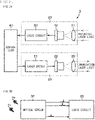
- FIG. 1 is a schematic configuration diagram illustrating an example of a distance measuring device according to an embodiment of the present disclosure.
- a distance measuring device 1 according to the present embodiment adopts, as a measurement method for measuring a distance to a subject 10 that is a measurement object, a ToF method that measures a time of flight until light (e.g., laser light having a peak wavelength in an infrared wavelength region) emitted toward the subject 10 returns by being reflected by the subject 10.
- the distance measuring device 1 according to the present embodiment includes a light source 20 and a light reception device 30.
- the light reception device 30 it is possible to use a light reception device according to an embodiment of the present disclosure to be described later.
- FIG. 2A and FIG. 2B each illustrate an example of a specific configuration of the distance measuring device 1 according to the present embodiment.
- the light source 20 includes, for example, a laser driver 21, a laser light source 22, and a diffusion lens 23, and irradiates the subject 10 with laser light.
- the laser driver 21 drives the laser light source 22 under control by the controller 40.
- the laser light source 22 includes, for example, a laser diode, and is driven by the laser driver 21 to emit laser light.
- the diffusion lens 23 diffuses the laser light emitted from the laser light source 22 to irradiate the subject 10 with the laser light.
- the light reception device 30 includes a light-receiving lens 31, an optical sensor 32 that is a light-receiving section, and a logic circuit 33, and receives reflected laser light.
- the reflected laser light is irradiation laser light by a laser irradiation section 20 that returns by being reflected by the subject 10.
- the light-receiving lens 31 condenses the reflected laser light from the subject 10 onto a light-receiving surface of the optical sensor 32.
- the optical sensor 32 receives the reflected laser light from the subject 10 having passed through the light-receiving lens 31 in pixel units and performs photoelectric conversion of the reflected laser light.
- the optical sensor 32 it is possible to use a two-dimensional array sensor (a so-called area sensor) including pixels that each include a light-receiving element and are two-dimensionally arranged in a matrix (in an array).
- the controller 40 includes, for example, a CPU (Central Processing Unit) or the like.
- the controller 40 controls the light source 20 and the light reception device 30, and measures a time t until laser light emitted from the light source 20 toward the subject 10 returns by being reflected by the subject 10. It is possible to determine a distance L to the subject 10 on the basis of the time t.
- a timer starts at a timing at which the light source 20 emits pulsed light, and stops the timer at a timing at which the light reception device 30 receives the pulsed light, thereby measuring the time t.
- the light source 20 may emit pulsed light at predetermined intervals, and the light reception device 30 may detect intervals at which the pulsed light is received, thereby measuring the time t from a phase difference between intervals at which light is emitted and intervals at which light is received.
- the time is measured by executing time measurement a plurality of times and detecting a peak of a histogram in which times obtained by the plurality of times of measurement are cumulated.
- a sensor including, as the light-receiving element of the pixel, an element that generates a signal in response to reception of a photon, for example, an SPAD (Single Photon Avalanche Diode: single-photon avalanche diode) element is used as the optical sensor 32.
- the light reception device 30 has a configuration in which the light-receiving element of the pixel includes an SPAD element.
- the light-receiving element is not limited to the SPAD element, and may include any of various elements such as an APD (Avalanche Photo Diode) and a CAPD (Current Assisted Photonic Demodulator).
- FIG. 3 illustrates an example of a basic pixel circuit in the light reception device 30 using the SPAD element. Here, a basic configuration of one pixel is illustrated.
- a basic pixel circuit of a pixel 50 using an SPAD element has a configuration in which a SPAD element 51 has a cathode electrode coupled to a terminal 52 supplied with a power supply voltage V DD via a P-type MOS transistor Q L that is a load, and an anode electrode coupled to a terminal 53 supplied with an anode voltage V bd .
- a large negative voltage that causes avalanche multiplication is applied as the anode voltage V bd .
- a capacitive element C is coupled between the anode electrode and a ground.
- the cathode voltage V CA of the SPAD element 51 is derived as an SPAD output (a pixel output) via a CMOS inverter 54 including a P-type MOS transistor Q p and an N-type MOS transistor Q n that are coupled in series to each other.
- a voltage equal to or higher than a breakdown voltage V BD is applied to the SPAD element 51.
- An excess voltage equal to or higher than the breakdown voltage V BD is called an excess bias voltage V EX , and is generally about a voltage of 2 V to 5 V.
- the SPAD element 51 operates in a region called Geiger mode in which there is no DC steady point.
- FIG. 4A illustrates I (current)-V (voltage) characteristics of a PN junction of the SPAD element 51.
- the cathode voltage V CA decreases and a voltage between terminals of the SPAD element 51 becomes the breakdown voltage V BD of a PN diode
- the avalanche current stops.
- electrons generated and accumulated by the avalanche multiplication are discharged by a resistive element R (or the P-type MOS transistor Q L ) that is a load, and the cathode voltage V CA recovers to the power supply voltage V DD , and returns to an initial state.
- the pair In a case where light is incident on the SPAD element 51 and at least one pair of an electron and a hole is generated, the pair causes generation of an avalanche current.
- PDE photon detection efficiency
- the detection efficiency PDE at which this photon is detectable is generally about several % to about 20%.
- the cathode voltage V CA is waveform-shaped by the CMOS inverter 54, and a pulse signal having a pulse width T with the arrival time of one photon as a start point is the SPAD output (pixel output).
- the light reception device includes a light-receiving section including the pixels 50 having the configuration described above that are two-dimensionally arranged in a matrix. It can be said that the light-receiving section including the two-dimensionally arranged pixels 50 corresponds to the optical sensor 32 in FIG. 2A .
- FIG. 5 is a schematic configuration diagram illustrating an example of the light reception device according to the embodiment of the present disclosure.
- the light reception device 30 includes a light-receiving section 60 including the pixels 50.
- the pixels 50 each include, as a light-receiving element, an element that generates a signal in response to reception of a photon, for example, the SPSD element 51, and are two-dimensionally arranged in a matrix.
- the light reception device 30 according to the present embodiment has a system configuration including a row selector 70, a column selector 80, a readout circuit section 90, a controller 40, and the like in addition to the light-receiving section 60.
- the row selector 70 selects, as a unit, one pixel row or a plurality of pixel rows of the pixels 50 of the light-receiving section 50 on the basis of a V control signal supplied from outside of the light reception device 30.
- V control signals 000[2:0] to 062[2:0] are used as the V control signal.
- the column selector 80 selects the pixels 50 of the light-receiving section 60 in pixel units on the basis of an H control signal supplied from outside of the light reception device 30.
- H control signals EN_SPAD_H0[2:0] to EN_SPAD_H198[2:0] are used as the H control signal.
- the readout circuit section 90 reads out signals of the pixels 50 selected in pixel units by the column selector 80 in the one pixel row or the plurality of pixel rows selected by the row selector 70, and performs predetermined processing on the signals, and thereafter outputs the signals to outside of the light reception device 30.
- the controller 40 performs control of pixel selection by the column selector 80, and readout control of the signals (pixel signals) of the pixels 50 by the readout circuit section 90 on the basis of a synchronization signal S_SYNC, a control signal LD_NUM, timing signals TRG_I and PRE_TRG, and the selection signal SEL supplied from outside of the light reception device 30.
- the light reception device 30 in a case where one pixel row or a plurality of pixel rows of the pixels 50 of the light-receiving section 60 are selected as a unit, and signals of all the pixels in a thus-selected region are read out at once, all the pixels in the selected pixel row or rows are simultaneously driven to increase a peak current. Furthermore, in addition to simultaneously driving all the pixels in the selected pixel row or rows, even in the readout circuit section that processes the read pixel signals, all circuit portions corresponding to all the pixels perform a processing operation. As a result, power consumption is increased.
- the signals 50 of the pixels in a pixel row (one pixel row or a plurality of pixel rows) selected by the row selector 70 are read out in a time division manner for each region including a plurality of pixels as a unit.
- the column selector 80 selects a plurality of pixels as a unit from the pixels 50 in the pixel row selected by the row selector 70 under control by the controller 40.
- the readout circuit section 90 reads out the signals of the pixels 50 in a time division manner for each region including, as a unit, the plurality of pixels selected by the column selector 80 under control by the controller 40.
- control lines in a row direction are divided for each pixel 50, which makes it possible to freely perform switching ON/OFF in pixel units by the column selector 80.
- switching ON/OFF in pixel units by the column selector 80 is performed by control based on the H control signal supplied from outside to select a plurality of pixels as a unit.
- signals of the pixels 50 in regions each including, as a unit, the plurality of pixels are read out in a time division manner.
- the controller 40 controls the row selector 70 to select, as a unit, one pixel row or a plurality of pixel rows of the pixels 50 of the light-receiving section 60 (step S11).
- the column selector 80 is controlled to select the pixels 50 in the selected pixel row or rows in units of regions each including, as a unit, a plurality of pixels (step S12).
- the controller 40 controls the readout circuit section 90 to read out the signals of the pixels 50 in a time division manner for each selected region (step S13).
- the light reception device 30 for the signals of the pixels 50 in a pixel row (one pixel row or a plurality of pixel rows) selected by the row selector 70, readout of pixel signals is performed in a time division manner for each region including, as a unit, a plurality of pixels. Performing readout of the pixel signals in a time division manner for each region selected by the column selector 80 in such a manner makes it possible to reduce power consumption, as compared with a case where signals of all pixels in one pixel row or a plurality of pixel rows are read out at once.
- An example 1 is a circuit example (a pixel circuit example) of the pixel 50 used in the light reception device 30 according to the embodiment of the present disclosure.
- FIG. 7 illustrates an example of a configuration of a pixel circuit according to the example 1.
- the pixel 50 according to the example 1 includes a first circuit section 50A and a second circuit section 50B.
- the first circuit section 50A includes a switch element SW and two N-type MOS transistors Q V and Q H , in addition to the P-type MOS transistor Q L (a load) and the CMOS inverter 54 in a basic pixel circuit illustrated in FIG. 3 .
- the CMOS inverter 54 is a CMOS inverter including the P-type MOS transistor Q p and the N-type MOS transistor Q n in FIG. 3 that are coupled in series to each other.
- the switch element SW is a quench switch, and stops an avalanche phenomenon by lowering a voltage applied to the SPAD sensor 51 to a breakdown voltage by a quenching operation.
- Each of the two N-type MOS transistors Q V and Q H is coupled between a terminal T coupled to the cathode electrode of the SPAD element 51 and a reference potential node (e.g., a ground GND).
- One N-type MOS transistor Q V is a row selection switch element for selecting the pixels 50 in pixel row units.
- the other N-type MOS transistor Q H is a column selection switch element for selecting the pixels 50 in pixel column units.
- the N-type MOS transistor Q V for row selection is turned to a non-conduction state in response to a scanning signal XEN_SPAD_V supplied from the row selector 70 in FIG. 5 to turn the terminal T to an open state, thereby selecting the pixels 50 in pixel row units.
- the N-type MOS transistor Q H for column selection is turned to the non-conduction state in response to a scanning signal XEN_SPAD_H supplied from the column selector 80 in FIG. 5 to turn the terminal T to the open state, thereby selecting the pixels 50 in pixel column units.
- the N-type MOS transistor Q H for column selection makes it possible to select, in pixel units, the pixels 50 in one pixel row or a plurality of pixel rows selected by the row selector 70.
- the N-type MOS transistor Q H for column selection is turned to a conduction state to turn a potential of the terminal T to a ground potential, thereby powering off the pixel 50 to turn the pixel 50 to a unselected state.
- power to the pixel 50 is turned to a shutoff state by an action of the N-type MOS transistor Q H makes it possible to achieve reduction in power consumption.
- the second circuit section 50B of the pixel 50 according to the example 1 has a circuit configuration including a level shift circuit 55, an 3-input NAND circuit 56, a 2-input OR circuit 57, an inverter circuit 58, and an inverter circuit 59.
- the voltage V CA of the terminal T passes through the CMOS inverter 54, and thereafter is level shifted by the level shift circuit 55 to become an inversion input (a firs input) of the 3-input NAND circuit 56.
- a control signal EN_C and a control signal EN_F are a second input and a third input.
- the control signal EN_C is a signal for control in a column direction (a vertical direction).
- the control signal EN_F is a signal for control of the row direction (a horizontal direction).
- a gate of the NAND circuit 56 opens when both the control signal EN_C and the control signal EN_F are logic "1".
- An output of the NAND circuit 56 is an inversion input (a first input) of the 2-input OR circuit 57.
- a control signal I_OR supplied from outside of the pixel 50, for example, the controller 40 in FIG. 5 is a second input.
- the control signal I_OR is a signal for controlling whether to enable or disable readout of the signal of the pixel 50.
- An output of the OR circuit 57 is outputted as a pixel signal O_SPAD via the inverter circuit 58 and the inverter circuit 59.
- the pixel circuit according to the example 1 has a configuration including the column selection switch element that turns each pixel to a selected state in response to the scanning signal XEN_SPAD_H supplied from the column selector 80, that is, the N-type MOS transistor Q H .
- This makes it possible to select the pixels 50 in one pixel row or a plurality of pixel rows selected by the row selector 70 in units of regions each including, as a unit, a plurality of pixels, and read out the signals of pixels for each region.
- power to the pixel 50 is turned to the shutoff state by an action of the N-type MOS transistor Q H , which makes it possible to achieve power saving.
- An example 2 is a configuration example of the readout circuit section 90 used in the light reception device 30 according to the embodiment of the present disclosure.
- FIG. 8 illustrates an example of a configuration of the readout circuit section 90 according to the example 2.
- the light-receiving section 60 having a 48 horizontal ⁇ 24 vertical pixel arrangement is illustrated as an example.
- each of control lines where a horizontal scanning signal XEN_SPAD_H, a vertical scanning signal XEN_SPAD_V, and a control signal EN_C are transmitted is wired for each pixel to the 48 horizontal ⁇ 24 vertical pixel arrangement
- each of control lines where a control signal EN_F is transmitted is wired for every three pixels to the 48 horizontal ⁇ 24 vertical pixel arrangement.
- regions each including 48 pixels as a unit are regions ROI0, ROI1, ROI2, and ROI3, and the region ROI1 among them is a region to be selected.
- the readout circuit section 90 processes the signals of the pixels 50 for each of the regions ROI (ROI0/ROI1/ROI2/ROI3) selected by the column selector 80.
- a circuit portion of the readout circuit section 90 corresponds to the region ROI selected by the column selector 80, and the readout circuit section 90 is divided into four, that is, a circuit portion 90A, a circuit portion 90B, a circuit portion 90C, and a circuit portion 90D.
- the controller 40 controls the readout circuit section 90 to turn a circuit portion (the circuit portion 90B in this example) corresponding to the region ROI selected by the column selector 80 to an activated state and turn the circuit portion 90A, the circuit portion 90C, and the circuit portion 90D other than the circuit portion 90B to an inactivated state.
- a clock system is divided for each of the circuit portions, and a power supply island is also separated, which makes it possible to perform switching of activation/inactivation for each of the circuit portions.
- the readout circuit section 90 according to the example 2 is divided into the circuit portions corresponding to the regions ROI selected by the column selector 80, and under control by the controller 40, the circuit portions other than the circuit portion corresponding to the region ROI selected by the column selector 80 are turned to the inactivated state by turning OFF a clock and turning OFF a power supply. This makes it possible to also achieve power saving in the readout circuit section 90 in addition to power saving in the pixels 50.
- An example 3 is a control example by the controller 40.
- the controller 40 performs control of pixel selection by the column selector 80, and readout control of the signals (pixel signals) of the pixels 50 by the readout circuit section 90 on the basis of the synchronization signal S_SYNC, the control signal LD_NUM, the timing signals TRG_I and PRE_TRG, and the selection signal SEL.
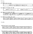
- the control signal LD_NUM is a signal for determining the division number of the regions RIO to be selected by the column selector 80
- the selection signal SEL is a signal for specifying which region ROI is to be selected to read out the pixel signals.
- the division number of the regions RIO to be selected by the column selector 80 is the number of the regions ROI including, as a unit, a plurality of pixels in one pixel row or a plurality of pixel rows selected by the column selector 80.
- the controller 40 first sets the division number of the region ROI to be selected by the column selector 80 on the basis of the control signal LD_NUM, as illustrated in FIG. 9A .
- the region ROI0 and the region ROI1 are readout regions. Then, the region ROI0 and the region ROI1 are alternately turned to an operation state in synchronization with the timing signal TRG I to perform readout of the signals of the pixels 50.
- an ambient light component is acquired in an entire processing range (the region ROI0 and the region ROI1 in this example) regardless of the division mode of the regions ROI in synchronization with the timing signal PRE_TRG.
- the ambient light component for example, processing of taking a difference with respect to the pixel signals obtained from the region ROI0 and the region ROI1 is performed in the readout circuit section 90. This makes it possible to eliminate the influence of the ambient light.
- the division number of the regions ROI is set by the control signal LD_NUM, and the regions ROI are specified by the selection signal SEL; however, the regions ROI may be specified only by the selection signal SEL.
- a single region ROI may be specified only by the selection signal SEL, and as illustrated in a lower stage of FIG. 10B , a plurality of regions ROI may be specified only by the selection signal SEL.
- the controller 40 is able to specify the region ROI where the signals of the pixels 50 are to be read out in accordance with a set value of the selection signal SEL. That is, the controller 40 is able to optionally specify a region where the signals of the pixels 50 are to be read out among a plurality of set regions, in accordance with the value of the selection signal SEL.
- An example 4 is an example in which signals of the regions ROI are read out in a time division manner, and is an example in a division mode of division into four (ROIO/ROI1/ROI2/ROI3).
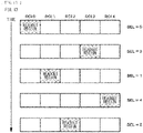
- FIG. 11 illustrates an operation example of time-division readout according to the example 4.
- the region ROI0, the region ROI1, the region ROI2, and the region ROI3 are selected in region units, and the signals of the pixels 50 in the selected region ROI are read out.
- the controller 40 reads out the signals of the pixels 50 in one pixel row or a plurality of pixel rows selected by the row selector 70 in a time division manner for each region.
- a region away from a previous readout region be set as a present readout region.
- the controller 40 first sets the region ROI1 as the readout region, and then skips the region ROI2 and sets, as the readout region, the region ROI3 away from the region ROI1.
- the controller 40 skips the region ROI1 and the region ROI2 and sets, as the readout region, the region ROI0 away from the region ROI3.
- the region ROI1 is skipped, and the region ROI2 away from the region ROI00 is set as the readout region.
- FIG. 13 an operation example of time division readout in a case of division into five is illustrated in FIG. 13 .
- the readout regions are set in order of the region ROI0 ⁇ the region ROI3 ⁇ the region ROI1 ⁇ the region ROI4 ⁇ the region ROI2, and readout is performed in a time division manner for each region, which makes it possible to suppress the influence of light emission of the previous readout region in reading out the signals of the pixels 50 in a presently set region.
- An example 5 is an example in which a peak of a histogram is selected.
- the time t is measured by executing time measurement a plurality of times and detecting a peak of a histogram in which times obtained by the plurality of times of measurement are cumulated, and the distance L to a subject is determined on the basis of the time t.
- FIG. 14A and FIG. 14B each illustrate a specific example of peak selection of the histogram according to the example 5.
- FIG. 14A is a waveform diagram in a case where in a present histogram acquisition period, a small peak is generated in a first peak portion by an influence of light emission of a previous readout region.
- filtering processing or the like is performed not to select (acquire) the small peak caused by the influence of light emission of the previous readout region.
- FIG. 14B is a waveform diagram in a case where a small peak is generated at a close distance by the influence of light emission of the previous readout region. In a case of a specific example illustrated in FIG. 14B , the small peak at the close distance is not selected (acquired).
- the technology of the present disclosure has been described with reference to preferred embodiments, the technology of the present disclosure is not limited to the embodiments.
- the configurations and structures of the light reception device and the distance measuring device described in the above embodiments are illustrative, and may be appropriately modified.
- the SPAD element is used as the light-receiving element
- the light-receiving element is not limited to the SPAD element, and even in a case where an element such as an APD and a CAPD is used, similar workings and effects are achievable.
- the technology according to the present disclosure is applicable to various products. A more specific application example is described below.
- the technology according to the present disclosure may be achieved in the form of a distance measuring device to be mounted to a mobile body of any kind such as an automobile, an electric vehicle, a hybrid electric vehicle, a motorcycle, a bicycle, a personal mobility, an airplane, a drone, a vessel, a robot, a construction machine, and an agricultural machine (tractor).
- FIG. 15 is a block diagram depicting an example of schematic configuration of a vehicle control system 7000 as an example of a mobile body control system to which the technology according to an embodiment of the present disclosure can be applied.
- the vehicle control system 7000 includes a plurality of electronic control units connected to each other via a communication network 7010.
- the vehicle control system 7000 includes a driving system control unit 7100, a body system control unit 7200, a battery control unit 7300, an outside-vehicle information detecting unit 7400, an in-vehicle information detecting unit 7500, and an integrated control unit 7600.
- the communication network 7010 connecting the plurality of control units to each other may, for example, be a vehicle-mounted communication network compliant with an arbitrary standard such as controller area network (CAN), local interconnect network (LIN), local area network (LAN), FlexRay, or the like.
- CAN controller area network
- LIN local interconnect network
- LAN local area network
- FlexRay or the like.
- Each of the control units includes: a microcomputer that performs arithmetic processing according to various kinds of programs; a storage section that stores the programs executed by the microcomputer, parameters used for various kinds of operations, or the like; and a driving circuit that drives various kinds of control target devices.
- Each of the control units further includes: a network interface (I/F) for performing communication with other control units via the communication network 7010; and a communication I/F for performing communication with a device, a sensor, or the like within and without the vehicle by wire communication or radio communication.
- I/F network interface
- the 15 includes a microcomputer 7610, a general-purpose communication I/F 7620, a dedicated communication I/F 7630, a positioning section 7640, a beacon receiving section 7650, an in-vehicle device I/F 7660, a sound/image output section 7670, a vehicle-mounted network I/F 7680, and a storage section 7690.
- the other control units similarly include a microcomputer, a communication I/F, a storage section, and the like.
- the driving system control unit 7100 controls the operation of devices related to the driving system of the vehicle in accordance with various kinds of programs.
- the driving system control unit 7100 functions as a control device for a driving force generating device for generating the driving force of the vehicle, such as an internal combustion engine, a driving motor, or the like, a driving force transmitting mechanism for transmitting the driving force to wheels, a steering mechanism for adjusting the steering angle of the vehicle, a braking device for generating the braking force of the vehicle, and the like.
- the driving system control unit 7100 may have a function as a control device of an antilock brake system (ABS), electronic stability control (ESC), or the like.
- ABS antilock brake system
- ESC electronic stability control
- the driving system control unit 7100 is connected with a vehicle state detecting section 7110.
- the vehicle state detecting section 7110 includes at least one of a gyro sensor that detects the angular velocity of axial rotational movement of a vehicle body, an acceleration sensor that detects the acceleration of the vehicle, and sensors for detecting an amount of operation of an accelerator pedal, an amount of operation of a brake pedal, the steering angle of a steering wheel, an engine speed or the rotational speed of wheels, and the like.
- the driving system control unit 7100 performs arithmetic processing using a signal input from the vehicle state detecting section 7110, and controls the internal combustion engine, the driving motor, an electric power steering device, the brake device, and the like.
- the body system control unit 7200 controls the operation of various kinds of devices provided to the vehicle body in accordance with various kinds of programs.
- the body system control unit 7200 functions as a control device for a keyless entry system, a smart key system, a power window device, or various kinds of lamps such as a headlamp, a backup lamp, a brake lamp, a turn signal, a fog lamp, or the like.
- radio waves transmitted from a mobile device as an alternative to a key or signals of various kinds of switches can be input to the body system control unit 7200.
- the body system control unit 7200 receives these input radio waves or signals, and controls a door lock device, the power window device, the lamps, or the like of the vehicle.
- the battery control unit 7300 controls a secondary battery 7310, which is a power supply source for the driving motor, in accordance with various kinds of programs.
- the battery control unit 7300 is supplied with information about a battery temperature, a battery output voltage, an amount of charge remaining in the battery, or the like from a battery device including the secondary battery 7310.
- the battery control unit 7300 performs arithmetic processing using these signals, and performs control for regulating the temperature of the secondary battery 7310 or controls a cooling device provided to the battery device or the like.
- the outside-vehicle information detecting unit 7400 detects information about the outside of the vehicle including the vehicle control system 7000.
- the outside-vehicle information detecting unit 7400 is connected with at least one of an imaging section 7410 and an outside-vehicle information detecting section 7420.
- the imaging section 7410 includes at least one of a time-of-flight (ToF) camera, a stereo camera, a monocular camera, an infrared camera, and other cameras.
- ToF time-of-flight
- the outside-vehicle information detecting section 7420 includes at least one of an environmental sensor for detecting current atmospheric conditions or weather conditions and a peripheral information detecting sensor for detecting another vehicle, an obstacle, a pedestrian, or the like on the periphery of the vehicle including the vehicle control system 7000.
- the environmental sensor may be at least one of a rain drop sensor detecting rain, a fog sensor detecting a fog, a sunshine sensor detecting a degree of sunshine, and a snow sensor detecting a snowfall.
- the peripheral information detecting sensor may be at least one of an ultrasonic sensor, a radar device, and a LIDAR device (Light detection and Ranging device, or Laser imaging detection and ranging device).
- Each of the imaging section 7410 and the outside-vehicle information detecting section 7420 may be provided as an independent sensor or device, or may be provided as a device in which a plurality of sensors or devices are integrated.
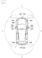
- FIG. 16 depicts an example of installation positions of the imaging section 7410 and the outside-vehicle information detecting section 7420.
- Imaging sections 7910, 7912, 7914, 7916, and 7918 are, for example, disposed at at least one of positions on a front nose, sideview mirrors, a rear bumper, and a back door of the vehicle 7900 and a position on an upper portion of a windshield within the interior of the vehicle.
- the imaging section 7910 provided to the front nose and the imaging section 7918 provided to the upper portion of the windshield within the interior of the vehicle obtain mainly an image of the front of the vehicle 7900.
- the imaging sections 7912 and 7914 provided to the sideview mirrors obtain mainly an image of the sides of the vehicle 7900.
- the imaging section 7916 provided to the rear bumper or the back door obtains mainly an image of the rear of the vehicle 7900.
- the imaging section 7918 provided to the upper portion of the windshield within the interior of the vehicle is used mainly to detect a preceding vehicle, a pedestrian, an obstacle, a signal, a traffic sign, a lane, or the like.
- FIG. 16 depicts an example of photographing ranges of the respective imaging sections 7910, 7912, 7914, and 7916.
- An imaging range a represents the imaging range of the imaging section 7910 provided to the front nose.
- Imaging ranges b and c respectively represent the imaging ranges of the imaging sections 7912 and 7914 provided to the sideview mirrors.
- An imaging range d represents the imaging range of the imaging section 7916 provided to the rear bumper or the back door.
- a bird's-eye image of the vehicle 7900 as viewed from above can be obtained by superimposing image data imaged by the imaging sections 7910, 7912, 7914, and 7916, for example.
- Outside-vehicle information detecting sections 7920, 7922, 7924, 7926, 7928, and 7930 provided to the front, rear, sides, and corners of the vehicle 7900 and the upper portion of the windshield within the interior of the vehicle may be, for example, an ultrasonic sensor or a radar device.
- the outside-vehicle information detecting sections 7920, 7926, and 7930 provided to the front nose of the vehicle 7900, the rear bumper, the back door of the vehicle 7900, and the upper portion of the windshield within the interior of the vehicle may be a LIDAR device, for example.
- These outside-vehicle information detecting sections 7920 to 7930 are used mainly to detect a preceding vehicle, a pedestrian, an obstacle, or the like.
- the outside-vehicle information detecting unit 7400 makes the imaging section 7410 image an image of the outside of the vehicle, and receives imaged image data.
- the outside-vehicle information detecting unit 7400 receives detection information from the outside-vehicle information detecting section 7420 connected to the outside-vehicle information detecting unit 7400.
- the outside-vehicle information detecting section 7420 is an ultrasonic sensor, a radar device, or a LIDAR device
- the outside-vehicle information detecting unit 7400 transmits an ultrasonic wave, an electromagnetic wave, or the like, and receives information of a received reflected wave.
- the outside-vehicle information detecting unit 7400 may perform processing of detecting an object such as a human, a vehicle, an obstacle, a sign, a character on a road surface, or the like, or processing of detecting a distance thereto.
- the outside-vehicle information detecting unit 7400 may perform environment recognition processing of recognizing a rainfall, a fog, road surface conditions, or the like on the basis of the received information.
- the outside-vehicle information detecting unit 7400 may calculate a distance to an object outside the vehicle on the basis of the received information.
- the outside-vehicle information detecting unit 7400 may perform image recognition processing of recognizing a human, a vehicle, an obstacle, a sign, a character on a road surface, or the like, or processing of detecting a distance thereto.
- the outside-vehicle information detecting unit 7400 may subject the received image data to processing such as distortion correction, alignment, or the like, and combine the image data imaged by a plurality of different imaging sections 7410 to generate a bird's-eye image or a panoramic image.
- the outside-vehicle information detecting unit 7400 may perform viewpoint conversion processing using the image data imaged by the imaging section 7410 including the different imaging parts.
- the in-vehicle information detecting unit 7500 detects information about the inside of the vehicle.
- the in-vehicle information detecting unit 7500 is, for example, connected with a driver state detecting section 7510 that detects the state of a driver.
- the driver state detecting section 7510 may include a camera that images the driver, a biosensor that detects biological information of the driver, a microphone that collects sound within the interior of the vehicle, or the like.
- the biosensor is, for example, disposed in a seat surface, the steering wheel, or the like, and detects biological information of an occupant sitting in a seat or the driver holding the steering wheel.
- the in-vehicle information detecting unit 7500 may calculate a degree of fatigue of the driver or a degree of concentration of the driver, or may determine whether the driver is dozing.
- the in-vehicle information detecting unit 7500 may subject an audio signal obtained by the collection of the sound to processing such as noise canceling processing or the like.
- the integrated control unit 7600 controls general operation within the vehicle control system 7000 in accordance with various kinds of programs.
- the integrated control unit 7600 is connected with an input section 7800.
- the input section 7800 is implemented by a device capable of input operation by an occupant, such, for example, as a touch panel, a button, a microphone, a switch, a lever, or the like.
- the integrated control unit 7600 may be supplied with data obtained by voice recognition of voice input through the microphone.
- the input section 7800 may, for example, be a remote control device using infrared rays or other radio waves, or an external connecting device such as a mobile telephone, a personal digital assistant (PDA), or the like that supports operation of the vehicle control system 7000.
- the input section 7800 may be, for example, a camera.
- an occupant can input information by gesture.
- data may be input which is obtained by detecting the movement of a wearable device that an occupant wears.
- the input section 7800 may, for example, include an input control circuit or the like that generates an input signal on the basis of information input by an occupant or the like using the above-described input section 7800, and which outputs the generated input signal to the integrated control unit 7600.
- An occupant or the like inputs various kinds of data or gives an instruction for processing operation to the vehicle control system 7000 by operating the input section 7800.
- the storage section 7690 may include a read only memory (ROM) that stores various kinds of programs executed by the microcomputer and a random access memory (RAM) that stores various kinds of parameters, operation results, sensor values, or the like.
- ROM read only memory
- RAM random access memory
- the storage section 7690 may be implemented by a magnetic storage device such as a hard disc drive (HDD) or the like, a semiconductor storage device, an optical storage device, a magneto-optical storage device, or the like.
- the general-purpose communication I/F 7620 is a communication I/F used widely, which communication I/F mediates communication with various apparatuses present in an external environment 7750.
- the general-purpose communication I/F 7620 may implement a cellular communication protocol such as global system for mobile communications (GSM), worldwide interoperability for microwave access (WiMAX), long term evolution (LTE)), LTE-advanced (LTE-A), or the like, or another wireless communication protocol such as wireless LAN (referred to also as wireless fidelity (Wi-Fi), Bluetooth, or the like.
- GSM global system for mobile communications
- WiMAX worldwide interoperability for microwave access
- LTE long term evolution
- LTE-A LTE-advanced
- Wi-Fi wireless fidelity
- Bluetooth or the like.
- the general-purpose communication I/F 7620 may, for example, connect to an apparatus (for example, an application server or a control server) present on an external network (for example, the Internet, a cloud network, or a company-specific network) via a base station or an access point.
- the general-purpose communication I/F 7620 may connect to a terminal present in the vicinity of the vehicle (which terminal is, for example, a terminal of the driver, a pedestrian, or a store, or a machine type communication (MTC) terminal) using a peer to peer (P2P) technology, for example.
- an apparatus for example, an application server or a control server
- an external network for example, the Internet, a cloud network, or a company-specific network
- MTC machine type communication
- P2P peer to peer
- the dedicated communication I/F 7630 is a communication I/F that supports a communication protocol developed for use in vehicles.
- the dedicated communication I/F 7630 may implement a standard protocol such, for example, as wireless access in vehicle environment (WAVE), which is a combination of institute of electrical and electronic engineers (IEEE) 802.11p as a lower layer and IEEE 1609 as a higher layer, dedicated short range communications (DSRC), or a cellular communication protocol.
- WAVE wireless access in vehicle environment
- IEEE institute of electrical and electronic engineers
- DSRC dedicated short range communications
- the dedicated communication I/F 7630 typically carries out V2X communication as a concept including one or more of communication between a vehicle and a vehicle (Vehicle to Vehicle), communication between a road and a vehicle (Vehicle to Infrastructure), communication between a vehicle and a home (Vehicle to Home), and communication between a pedestrian and a vehicle (Vehicle to Pedestrian).
- the positioning section 7640 performs positioning by receiving a global navigation satellite system (GNSS) signal from a GNSS satellite (for example, a GPS signal from a global positioning system (GPS) satellite), and generates positional information including the latitude, longitude, and altitude of the vehicle.
- GNSS global navigation satellite system
- GPS global positioning system
- the positioning section 7640 may identify a current position by exchanging signals with a wireless access point, or may obtain the positional information from a terminal such as a mobile telephone, a personal handyphone system (PHS), or a smart phone that has a positioning function.
- the beacon receiving section 7650 receives a radio wave or an electromagnetic wave transmitted from a radio station installed on a road or the like, and thereby obtains information about the current position, congestion, a closed road, a necessary time, or the like.
- the function of the beacon receiving section 7650 may be included in the dedicated communication I/F 7630 described above.
- the in-vehicle device I/F 7660 is a communication interface that mediates connection between the microcomputer 7610 and various in-vehicle devices 7760 present within the vehicle.
- the in-vehicle device I/F 7660 may establish wireless connection using a wireless communication protocol such as wireless LAN, Bluetooth, near field communication (NFC), or wireless universal serial bus (WUSB).
- a wireless communication protocol such as wireless LAN, Bluetooth, near field communication (NFC), or wireless universal serial bus (WUSB).
- WUSB wireless universal serial bus
- the in-vehicle device I/F 7660 may establish wired connection by universal serial bus (USB), high-definition multimedia interface (HDMI), mobile high-definition link (MHL), or the like via a connection terminal (and a cable if necessary) not depicted in the figures.
- USB universal serial bus
- HDMI high-definition multimedia interface
- MHL mobile high-definition link
- the in-vehicle devices 7760 may, for example, include at least one of a mobile device and a wearable device possessed by an occupant and an information device carried into or attached to the vehicle.
- the in-vehicle devices 7760 may also include a navigation device that searches for a path to an arbitrary destination.
- the in-vehicle device I/F 7660 exchanges control signals or data signals with these in-vehicle devices 7760.
- the vehicle-mounted network I/F 7680 is an interface that mediates communication between the microcomputer 7610 and the communication network 7010.
- the vehicle-mounted network I/F 7680 transmits and receives signals or the like in conformity with a predetermined protocol supported by the communication network 7010.
- the microcomputer 7610 of the integrated control unit 7600 controls the vehicle control system 7000 in accordance with various kinds of programs on the basis of information obtained via at least one of the general-purpose communication I/F 7620, the dedicated communication I/F 7630, the positioning section 7640, the beacon receiving section 7650, the in-vehicle device I/F 7660, and the vehicle-mounted network I/F 7680.
- the microcomputer 7610 may calculate a control target value for the driving force generating device, the steering mechanism, or the braking device on the basis of the obtained information about the inside and outside of the vehicle, and output a control command to the driving system control unit 7100.
- the microcomputer 7610 may perform cooperative control intended to implement functions of an advanced driver assistance system (ADAS) which functions include collision avoidance or shock mitigation for the vehicle, following driving based on a following distance, vehicle speed maintaining driving, a warning of collision of the vehicle, a warning of deviation of the vehicle from a lane, or the like.
- ADAS advanced driver assistance system
- the microcomputer 7610 may perform cooperative control intended for automatic driving, which makes the vehicle to travel autonomously without depending on the operation of the driver, or the like, by controlling the driving force generating device, the steering mechanism, the braking device, or the like on the basis of the obtained information about the surroundings of the vehicle.
- the microcomputer 7610 may generate three-dimensional distance information between the vehicle and an object such as a surrounding structure, a person, or the like, and generate local map information including information about the surroundings of the current position of the vehicle, on the basis of information obtained via at least one of the general-purpose communication I/F 7620, the dedicated communication I/F 7630, the positioning section 7640, the beacon receiving section 7650, the in-vehicle device I/F 7660, and the vehicle-mounted network I/F 7680.
- the microcomputer 7610 may predict danger such as collision of the vehicle, approaching of a pedestrian or the like, an entry to a closed road, or the like on the basis of the obtained information, and generate a warning signal.
- the warning signal may, for example, be a signal for producing a warning sound or lighting a warning lamp.
- the sound/image output section 7670 transmits an output signal of at least one of a sound and an image to an output device capable of visually or auditorily notifying information to an occupant of the vehicle or the outside of the vehicle.
- an audio speaker 7710, a display section 7720, and an instrument panel 7730 are illustrated as the output device.
- the display section 7720 may, for example, include at least one of an on-board display and a head-up display.
- the display section 7720 may have an augmented reality (AR) display function.
- the output device may be other than these devices, and may be another device such as headphones, a wearable device such as an eyeglass type display worn by an occupant or the like, a projector, a lamp, or the like.
- the output device is a display device
- the display device visually displays results obtained by various kinds of processing performed by the microcomputer 7610 or information received from another control unit in various forms such as text, an image, a table, a graph, or the like.
- the audio output device converts an audio signal constituted of reproduced audio data or sound data or the like into an analog signal, and auditorily outputs the analog signal.
- control units connected to each other via the communication network 7010 in the example depicted in FIG. 15 may be integrated into one control unit.
- each individual control unit may include a plurality of control units.
- the vehicle control system 7000 may include another control unit not depicted in the figures.
- part or the whole of the functions performed by one of the control units in the above description may be assigned to another control unit. That is, predetermined arithmetic processing may be performed by any of the control units as long as information is transmitted and received via the communication network 7010.
- a sensor or a device connected to one of the control units may be connected to another control unit, and a plurality of control units may mutually transmit and receive detection information via the communication network 7010.
- the technology according to the present disclosure is applicable to the ToF camera. Then, applying the technology according to the present disclosure makes it possible to reduce power consumption in reading out a signal of each of pixels of a light-receiving section, which makes it possible to achieve, for example, a vehicle control system having low power consumption.
Landscapes
- Engineering & Computer Science (AREA)
- Physics & Mathematics (AREA)
- Computer Networks & Wireless Communication (AREA)
- General Physics & Mathematics (AREA)
- Radar, Positioning & Navigation (AREA)
- Remote Sensing (AREA)
- Multimedia (AREA)
- Signal Processing (AREA)
- Electromagnetism (AREA)
- Optical Radar Systems And Details Thereof (AREA)
- Transforming Light Signals Into Electric Signals (AREA)
- Measurement Of Optical Distance (AREA)
Abstract
Description
- The present disclosure relates to a light reception device, a method of controlling a light reception device, and a distance measuring device (a distance measurement device).
- There is a light reception device using, as a light-receiving element, an element that generates a signal in response to reception of a photon (see
PTL 1, for example). In a light reception device of this kind, as a measurement method for measuring a distance to a measurement object, a ToF (Time Of Flight) method is adopted which measures a time until light emitted toward the measurement object returns after being reflected by the measurement object. - PTL 1:
Japanese Unexamined Patent Application Publication No. 2016-211881 - Of the ToF, a direct ToF method directly calculates a distance from a time-of-flight difference of light. In the direct ToF method, processing of reading out a signal of each pixel of a light-receiving section is performed. The light-receiving section includes pixels that each include a light-receiving element and are two-dimensionally arranged in a matrix. On this occasion, in a case where one pixel row or a plurality of pixel rows of the pixels of the light-receiving section are selected as a unit, and signals of all the pixels in a thus-selected region are read out at once, power consumption is increased.
- Therefore, an object of the present disclosure is to provide a light reception device and a method of controlling a light reception device that make it possible to reduce power consumption in reading out a signal of each of pixels in a light-receiving section, and a distance measuring device that uses the light reception device.
- A light reception device of the present disclosure to achieve the above-described object includes:
- a light-receiving section including pixels two-dimensionally arranged in a matrix, the pixels each including a light-receiving element;
- a row selector that selects the pixels of the light-receiving section in units of one pixel row or a plurality of pixel rows;
- a column selector that selects the pixels in one pixel row or a plurality of pixel rows selected by the row selector in pixel units; and
- a controller that controls the column selector,
- the controller controlling the column selector to select the pixels in the one pixel row or the plurality of pixel rows selected by the row selector in units of regions each including a plurality of pixels as a unit, and read out signals of the pixels for each of the regions.
- A method of controlling a light reception device of the present disclosure to achieve the above-described object, the light reception device including
- a light-receiving section including pixels two-dimensionally arranged in a matrix, the pixels each including a light-receiving element,
- a row selector that selects the pixels of the light-receiving section in units of one pixel row or a plurality of pixel rows, and
- a column selector that selects the pixels in one pixel row or a plurality of pixel rows selected by the row selector in pixel units,
- the method including:
in control of the light reception device, controlling the column selector to select the pixels in the one pixel row or the plurality of pixel rows selected by the row selector in units of regions each including a plurality of pixels as a unit, and reading out signals of the pixels for each of the regions. - A distance measuring device of the present disclosure to achieve the above-described object includes:
- a light source that irradiates a measurement object with light; and
- a light reception device that detects light reflected by the measurement object, the light reception device including:
- a light-receiving section including pixels two-dimensionally arranged in a matrix, the pixels each including a light-receiving element,
- a row selector that selects the pixels of the light-receiving section in units of one pixel row or a plurality of pixel rows,
- a column selector that selects the pixels in one pixel row or a plurality of pixel rows selected by the row selector in pixel units, and
- a controller that controls the column selector,
- the controller controlling the column selector to select the pixels in the one pixel row or the plurality of pixel rows selected by the row selector in units of regions each including a plurality of pixels as a unit, and read out signals of the pixels for each of the regions.
-
- [
FIG. 1] FIG. 1 is a schematic configuration diagram illustrating an example of a distance measuring device according to an embodiment of the present disclosure. - [
FIG. 2] FIG. 2A and FIG. 2B are block diagrams each illustrating an example of a specific configuration of the distance measuring device according to the embodiment of the present disclosure. - [
FIG. 3] FIG. 3 is a circuit diagram illustrating an example of a basic pixel circuit using an SPAD element. - [
FIG. 4] FIG. 4A is a characteristic diagram illustrating current-voltage characteristics of a PN junction of the SPAD element, andFIG. 4B is a waveform diagram for description of a circuit operation of the pixel circuit. - [
FIG. 5] FIG. 5 is a schematic configuration diagram illustrating an example of a light reception device according to an embodiment of the present disclosure. - [
FIG. 6] FIG. 6 is a flowchart that describes a method of controlling the light reception device according to the embodiment of the present disclosure. - [
FIG. 7] FIG. 7 is a circuit diagram illustrating an example of a configuration of a pixel circuit according to an example 1. - [
FIG. 8] FIG. 8 is a schematic configuration diagram illustrating an example of a configuration of a readout circuit section according to an example 2. - [
FIG. 9] FIG. 9A is a diagram illustrating a correspondence between a control signal LD_NUM and the division number in a control example according to an example 3, and -
FIG. 9B is a diagram illustrating an operation image when LD_NUM = 1, that is, when the division number = 2. - [
FIG. 10] FIG. 10A is a diagram illustrating an example of setting of the division number of regions ROI by the control signal LD_NUM and specification of the region ROI by a selection signal SEL, andFIG. 10B is a diagram illustrating an example in which the region ROI is specified only by the selection signal SEL. - [
FIG. 11] FIG. 11 is a diagram illustrating an operation example of time-division readout according to an example 4 in a case of division into four. - [
FIG. 12] FIG. 12 is a diagram that describes a malfunction in a case where adjacent regions are set as readout regions in order. - [
FIG. 13] FIG. 13 is a diagram illustrating an operation example of time-division readout in a case of division into five. - [
FIG. 14] FIG. 14A and FIG. 14B are waveform diagrams that each describe a specific example of peak selection of a histogram according to an example 5. - [
FIG. 15] FIG. 15 is a block diagram illustrating an example of a schematic configuration of a vehicle control system that is an example of a mobile body control system to which the technology according to the present disclosure is applicable. - [
FIG. 16] FIG. 16 is a diagram illustrating an example of an installation position of the distance measuring device. - Hereinafter, modes for carrying out the technology of the present disclosure (hereinafter referred to as "embodiments") are described in detail with reference to the drawings. The technology of the present disclosure is not limited to the embodiments, and various numerical values and the like in the embodiments are illustrative. In the following description, the same components, or components having the same function are denoted by the same reference signs, and redundant description is omitted. It is to be noted that description is given in the following order.
- 1. General Description of Light Reception Device and Distance Measuring Device of Present Disclosure
- 2. Distance Measuring device According to Embodiment
- 2-1. Specific Configuration Example of Distance Measuring Device
- 2-2. Basic Pixel Circuit Example Using SPAD Element
- 2-3. Circuit Operation Example of Pixel Circuit Using SPAD Element
- 3. Light Reception Device According to Embodiment
- 3-1. Example 1 (A configuration example of a pixel circuit)
- 3-2. Example 2 (A configuration example of a readout circuit section)
- 3-3. Example 3 (A control example by a controller)
- 3-4. Example 4 (An example in which signals of regions ROI are read out in a time division manner)
- 3-5. Example 5 (An example in which a peak of a histogram is selected)
- 4. Modification Examples
- 5. Application Example of Technology According to Present Disclosure (An example of a mobile body)
- 6. Possible Configurations of Present Disclosure
- A light reception device and a distance measuring device of the present disclosure may have a configuration including a readout circuit section that processes a signal read out from each of pixels of a light-receiving section. Then, the readout circuit section may be configured to process signals read out from the pixels of the light-receiving section for each region selected by a column selector. In addition, a controller may be configured to control the readout circuit section to turn a circuit portion other than a circuit portion corresponding to the region selected by the column selector to an inactivated state.
- The light reception device and the distance measuring device of the present disclosure including the preferred configurations described above may have a configuration in which the pixels each include a column selection switch element that turns each pixel to a selected state in response to a scanning signal supplied from the column selector. In addition, the column selection switch element may be configured to turn the pixel to an unselected state by turning power to the pixel to a shutoff state.
- In addition, in the light reception device and the distance measuring device of the present disclosure including the preferred configurations described above, the controller may be configured to be able to set the number of regions each including a plurality of pixels as a unit in one pixel row or a plurality of pixel rows selected by the row selector. Furthermore, the controller may be configured to be able to optionally specify a region where signals of pixels are to be read out, among a plurality of set regions.
- In addition, in the light reception device and the distance measuring device of the present disclosure including the preferred configurations described above, the controller may be configured to set, as a present readout region, a region away from a previous readout region in a case where the signals of the pixels in the one pixel row or the plurality of pixel rows selected by the row selector are read out in a time division manner for each region.
- In addition, in the light reception device and the distance measuring device of the present disclosure including the preferred configurations described above, the light-receiving element may be configured to include an element that generates a signal in response to reception of a photon, and preferably a single-photon avalanche diode.
-
FIG. 1 is a schematic configuration diagram illustrating an example of a distance measuring device according to an embodiment of the present disclosure. Adistance measuring device 1 according to the present embodiment adopts, as a measurement method for measuring a distance to a subject 10 that is a measurement object, a ToF method that measures a time of flight until light (e.g., laser light having a peak wavelength in an infrared wavelength region) emitted toward the subject 10 returns by being reflected by the subject 10. In order to implement distance measurement by the ToF, thedistance measuring device 1 according to the present embodiment includes alight source 20 and alight reception device 30. Furthermore, as thelight reception device 30, it is possible to use a light reception device according to an embodiment of the present disclosure to be described later. -
FIG. 2A and FIG. 2B each illustrate an example of a specific configuration of thedistance measuring device 1 according to the present embodiment. Thelight source 20 includes, for example, alaser driver 21, alaser light source 22, and adiffusion lens 23, and irradiates the subject 10 with laser light. Thelaser driver 21 drives thelaser light source 22 under control by thecontroller 40. Thelaser light source 22 includes, for example, a laser diode, and is driven by thelaser driver 21 to emit laser light. Thediffusion lens 23 diffuses the laser light emitted from thelaser light source 22 to irradiate the subject 10 with the laser light. - The
light reception device 30 includes a light-receivinglens 31, anoptical sensor 32 that is a light-receiving section, and alogic circuit 33, and receives reflected laser light. The reflected laser light is irradiation laser light by alaser irradiation section 20 that returns by being reflected by the subject 10. The light-receivinglens 31 condenses the reflected laser light from the subject 10 onto a light-receiving surface of theoptical sensor 32. Theoptical sensor 32 receives the reflected laser light from the subject 10 having passed through the light-receivinglens 31 in pixel units and performs photoelectric conversion of the reflected laser light. As theoptical sensor 32, it is possible to use a two-dimensional array sensor (a so-called area sensor) including pixels that each include a light-receiving element and are two-dimensionally arranged in a matrix (in an array). - An output signal of the
optical sensor 32 is supplied to thecontroller 40 via thelogic circuit 33. Thecontroller 40 includes, for example, a CPU (Central Processing Unit) or the like. Thecontroller 40 controls thelight source 20 and thelight reception device 30, and measures a time t until laser light emitted from thelight source 20 toward the subject 10 returns by being reflected by the subject 10. It is possible to determine a distance L to the subject 10 on the basis of the time t. - As a time measurement method, a timer starts at a timing at which the
light source 20 emits pulsed light, and stops the timer at a timing at which thelight reception device 30 receives the pulsed light, thereby measuring the time t. As another time measurement method, thelight source 20 may emit pulsed light at predetermined intervals, and thelight reception device 30 may detect intervals at which the pulsed light is received, thereby measuring the time t from a phase difference between intervals at which light is emitted and intervals at which light is received. The time is measured by executing time measurement a plurality of times and detecting a peak of a histogram in which times obtained by the plurality of times of measurement are cumulated. - Then, in the present embodiment, a sensor including, as the light-receiving element of the pixel, an element that generates a signal in response to reception of a photon, for example, an SPAD (Single Photon Avalanche Diode: single-photon avalanche diode) element is used as the
optical sensor 32. That is, thelight reception device 30 according to the present embodiment has a configuration in which the light-receiving element of the pixel includes an SPAD element. It is to be noted that the light-receiving element is not limited to the SPAD element, and may include any of various elements such as an APD (Avalanche Photo Diode) and a CAPD (Current Assisted Photonic Demodulator). -
FIG. 3 illustrates an example of a basic pixel circuit in thelight reception device 30 using the SPAD element. Here, a basic configuration of one pixel is illustrated. - A basic pixel circuit of a
pixel 50 using an SPAD element has a configuration in which aSPAD element 51 has a cathode electrode coupled to a terminal 52 supplied with a power supply voltage VDD via a P-type MOS transistor QL that is a load, and an anode electrode coupled to a terminal 53 supplied with an anode voltage Vbd. As the anode voltage Vbd, a large negative voltage that causes avalanche multiplication is applied. A capacitive element C is coupled between the anode electrode and a ground. Then, the cathode voltage VCA of theSPAD element 51 is derived as an SPAD output (a pixel output) via aCMOS inverter 54 including a P-type MOS transistor Qp and an N-type MOS transistor Qn that are coupled in series to each other. - A voltage equal to or higher than a breakdown voltage VBD is applied to the
SPAD element 51. An excess voltage equal to or higher than the breakdown voltage VBD is called an excess bias voltage VEX, and is generally about a voltage of 2 V to 5 V. TheSPAD element 51 operates in a region called Geiger mode in which there is no DC steady point.FIG. 4A illustrates I (current)-V (voltage) characteristics of a PN junction of theSPAD element 51. - Next, description is given of an example of a circuit operation of the pixel circuit having the configuration described above with reference to a waveform diagram in
FIG. 4B . - In a state in which a current does not pass through the
SPAD element 51, a voltage having a value of VDD - Vbd is applied to theSPAD element 51. This voltage value (VDD - Vbd) is (VBD + VEX). Then, a dark electron generation rate DCR (Dark Count Rate) and electrons generated by the light irradiation cause avalanche multiplication at a PN junction section of theSPAD element 51, thereby generating an avalanche current. Such a phenomenon occurs stochastically even in a light-shielded state (that is, in a state in which no light is incident). This is the dark electron generation rate DCR. - In a case where the cathode voltage VCA decreases and a voltage between terminals of the
SPAD element 51 becomes the breakdown voltage VBD of a PN diode, the avalanche current stops. Then, electrons generated and accumulated by the avalanche multiplication are discharged by a resistive element R (or the P-type MOS transistor QL) that is a load, and the cathode voltage VCA recovers to the power supply voltage VDD, and returns to an initial state. - In a case where light is incident on the
SPAD element 51 and at least one pair of an electron and a hole is generated, the pair causes generation of an avalanche current. Thus, it is possible to detect even incidence of one photon at a certain detection efficiency PDE (photon detection efficiency). The detection efficiency PDE at which this photon is detectable is generally about several % to about 20%. - The above-described operations are repeated. In addition, in this series of operations, the cathode voltage VCA is waveform-shaped by the
CMOS inverter 54, and a pulse signal having a pulse width T with the arrival time of one photon as a start point is the SPAD output (pixel output). - Next, description is given of the light reception device according to the embodiment of the present disclosure that may be used in the
distance measuring device 1 having the configuration described above, and a method of controlling the light reception device. The light reception device according to the present embodiment includes a light-receiving section including thepixels 50 having the configuration described above that are two-dimensionally arranged in a matrix. It can be said that the light-receiving section including the two-dimensionally arrangedpixels 50 corresponds to theoptical sensor 32 inFIG. 2A . -
FIG. 5 is a schematic configuration diagram illustrating an example of the light reception device according to the embodiment of the present disclosure. As illustrated inFIG. 5 , thelight reception device 30 according to the present embodiment includes a light-receivingsection 60 including thepixels 50. Thepixels 50 each include, as a light-receiving element, an element that generates a signal in response to reception of a photon, for example, theSPSD element 51, and are two-dimensionally arranged in a matrix. Thelight reception device 30 according to the present embodiment has a system configuration including arow selector 70, acolumn selector 80, areadout circuit section 90, acontroller 40, and the like in addition to the light-receivingsection 60. - The
row selector 70 selects, as a unit, one pixel row or a plurality of pixel rows of thepixels 50 of the light-receivingsection 50 on the basis of a V control signal supplied from outside of thelight reception device 30. Here, a case where V control signals 000[2:0] to 062[2:0] are used as the V control signal is exemplified. Thecolumn selector 80 selects thepixels 50 of the light-receivingsection 60 in pixel units on the basis of an H control signal supplied from outside of thelight reception device 30. Here, a case where H control signals EN_SPAD_H0[2:0] to EN_SPAD_H198[2:0] are used as the H control signal. - The
readout circuit section 90 reads out signals of thepixels 50 selected in pixel units by thecolumn selector 80 in the one pixel row or the plurality of pixel rows selected by therow selector 70, and performs predetermined processing on the signals, and thereafter outputs the signals to outside of thelight reception device 30. Thecontroller 40 performs control of pixel selection by thecolumn selector 80, and readout control of the signals (pixel signals) of thepixels 50 by thereadout circuit section 90 on the basis of a synchronization signal S_SYNC, a control signal LD_NUM, timing signals TRG_I and PRE_TRG, and the selection signal SEL supplied from outside of thelight reception device 30. - In the
light reception device 30 according to the present embodiment having the configuration described above, in a case where one pixel row or a plurality of pixel rows of thepixels 50 of the light-receivingsection 60 are selected as a unit, and signals of all the pixels in a thus-selected region are read out at once, all the pixels in the selected pixel row or rows are simultaneously driven to increase a peak current. Furthermore, in addition to simultaneously driving all the pixels in the selected pixel row or rows, even in the readout circuit section that processes the read pixel signals, all circuit portions corresponding to all the pixels perform a processing operation. As a result, power consumption is increased. - Accordingly, in the
light reception device 30 according to the present embodiment, thesignals 50 of the pixels in a pixel row (one pixel row or a plurality of pixel rows) selected by therow selector 70 are read out in a time division manner for each region including a plurality of pixels as a unit. Specifically, thecolumn selector 80 selects a plurality of pixels as a unit from thepixels 50 in the pixel row selected by therow selector 70 under control by thecontroller 40. Then, thereadout circuit section 90 reads out the signals of thepixels 50 in a time division manner for each region including, as a unit, the plurality of pixels selected by thecolumn selector 80 under control by thecontroller 40. - More specifically, control lines in a row direction (an H direction) are divided for each
pixel 50, which makes it possible to freely perform switching ON/OFF in pixel units by thecolumn selector 80. Then, switching ON/OFF in pixel units by thecolumn selector 80 is performed by control based on the H control signal supplied from outside to select a plurality of pixels as a unit. Then, signals of thepixels 50 in regions each including, as a unit, the plurality of pixels are read out in a time division manner. - Next, description is given of a method of controlling the
light reception device 30 according to the present embodiment to be executed under control by thecontroller 40 with reference to a flowchart inFIG. 6 . Thecontroller 40 controls therow selector 70 to select, as a unit, one pixel row or a plurality of pixel rows of thepixels 50 of the light-receiving section 60 (step S11). Next, thecolumn selector 80 is controlled to select thepixels 50 in the selected pixel row or rows in units of regions each including, as a unit, a plurality of pixels (step S12). Then, thecontroller 40 controls thereadout circuit section 90 to read out the signals of thepixels 50 in a time division manner for each selected region (step S13). - As described above, in the
light reception device 30 according to the present embodiment, for the signals of thepixels 50 in a pixel row (one pixel row or a plurality of pixel rows) selected by therow selector 70, readout of pixel signals is performed in a time division manner for each region including, as a unit, a plurality of pixels. Performing readout of the pixel signals in a time division manner for each region selected by thecolumn selector 80 in such a manner makes it possible to reduce power consumption, as compared with a case where signals of all pixels in one pixel row or a plurality of pixel rows are read out at once. - The following description is given of specific examples of the present embodiment for performing readout of pixel signals in a time division manner for each region including, as a unit, a plurality of pixels in order to achieve reduction in power consumption.
- An example 1 is a circuit example (a pixel circuit example) of the
pixel 50 used in thelight reception device 30 according to the embodiment of the present disclosure.FIG. 7 illustrates an example of a configuration of a pixel circuit according to the example 1. - The
pixel 50 according to the example 1 includes afirst circuit section 50A and asecond circuit section 50B. Thefirst circuit section 50A includes a switch element SW and two N-type MOS transistors QV and QH, in addition to the P-type MOS transistor QL (a load) and theCMOS inverter 54 in a basic pixel circuit illustrated inFIG. 3 . TheCMOS inverter 54 is a CMOS inverter including the P-type MOS transistor Qp and the N-type MOS transistor Qn inFIG. 3 that are coupled in series to each other. - The switch element SW is a quench switch, and stops an avalanche phenomenon by lowering a voltage applied to the
SPAD sensor 51 to a breakdown voltage by a quenching operation. - Each of the two N-type MOS transistors QV and QH is coupled between a terminal T coupled to the cathode electrode of the
SPAD element 51 and a reference potential node (e.g., a ground GND). One N-type MOS transistor QV is a row selection switch element for selecting thepixels 50 in pixel row units. The other N-type MOS transistor QH is a column selection switch element for selecting thepixels 50 in pixel column units. - The N-type MOS transistor QV for row selection is turned to a non-conduction state in response to a scanning signal XEN_SPAD_V supplied from the
row selector 70 inFIG. 5 to turn the terminal T to an open state, thereby selecting thepixels 50 in pixel row units. The N-type MOS transistor QH for column selection is turned to the non-conduction state in response to a scanning signal XEN_SPAD_H supplied from thecolumn selector 80 inFIG. 5 to turn the terminal T to the open state, thereby selecting thepixels 50 in pixel column units. - Providing the N-type MOS transistor QH for column selection makes it possible to select, in pixel units, the
pixels 50 in one pixel row or a plurality of pixel rows selected by therow selector 70. In addition, the N-type MOS transistor QH for column selection is turned to a conduction state to turn a potential of the terminal T to a ground potential, thereby powering off thepixel 50 to turn thepixel 50 to a unselected state. In an unselected pixel, power to thepixel 50 is turned to a shutoff state by an action of the N-type MOS transistor QH makes it possible to achieve reduction in power consumption. - The
second circuit section 50B of thepixel 50 according to the example 1 has a circuit configuration including alevel shift circuit 55, an 3-input NAND circuit 56, a 2-input ORcircuit 57, aninverter circuit 58, and aninverter circuit 59. - The voltage VCA of the terminal T passes through the
CMOS inverter 54, and thereafter is level shifted by thelevel shift circuit 55 to become an inversion input (a firs input) of the 3-input NAND circuit 56. In the 3-input NAND circuit 56, a control signal EN_C and a control signal EN_F are a second input and a third input. The control signal EN_C is a signal for control in a column direction (a vertical direction). The control signal EN_F is a signal for control of the row direction (a horizontal direction). A gate of theNAND circuit 56 opens when both the control signal EN_C and the control signal EN_F are logic "1". - An output of the
NAND circuit 56 is an inversion input (a first input) of the 2-input ORcircuit 57. In the 2-input ORcircuit 57, a control signal I_OR supplied from outside of thepixel 50, for example, thecontroller 40 inFIG. 5 is a second input. The control signal I_OR is a signal for controlling whether to enable or disable readout of the signal of thepixel 50. An output of theOR circuit 57 is outputted as a pixel signal O_SPAD via theinverter circuit 58 and theinverter circuit 59. - As described above, the pixel circuit according to the example 1 has a configuration including the column selection switch element that turns each pixel to a selected state in response to the scanning signal XEN_SPAD_H supplied from the
column selector 80, that is, the N-type MOS transistor QH. This makes it possible to select thepixels 50 in one pixel row or a plurality of pixel rows selected by therow selector 70 in units of regions each including, as a unit, a plurality of pixels, and read out the signals of pixels for each region. In addition, as for an unselected pixel, power to thepixel 50 is turned to the shutoff state by an action of the N-type MOS transistor QH, which makes it possible to achieve power saving. - An example 2 is a configuration example of the
readout circuit section 90 used in thelight reception device 30 according to the embodiment of the present disclosure.FIG. 8 illustrates an example of a configuration of thereadout circuit section 90 according to the example 2. - Here, for simplification of the drawing, the light-receiving
section 60 having a 48 horizontal × 24 vertical pixel arrangement is illustrated as an example. For example, each of control lines where a horizontal scanning signal XEN_SPAD_H, a vertical scanning signal XEN_SPAD_V, and a control signal EN_C are transmitted is wired for each pixel to the 48 horizontal × 24 vertical pixel arrangement, and each of control lines where a control signal EN_F is transmitted is wired for every three pixels to the 48 horizontal × 24 vertical pixel arrangement. These control signals are not illustrated for simplification of the drawing. - In the present example, for ease of understanding, the
row selector 70 selects thepixels 50 of the light-receivingsection 60, for example, in units of four pixel rows in the 48 horizontal × 24 vertical pixel arrangement. Then, under control by thecontroller 40, thecolumn selector 80 selects thepixels 50 of the light-receivingsection 60 in units of regions each including, as a unit, 12 pixels in a horizontal direction, that is, 48 (= horizontal 12 × vertical 4) pixels in total, and reads out pixel signals. Here, it is assumed that regions each including 48 pixels as a unit are regions ROI0, ROI1, ROI2, and ROI3, and the region ROI1 among them is a region to be selected. On this occasion, under scanning by thecolumn selector 80, power to each of thepixels 50 of the regions ROI0, ROI2, and ROI3 other than the region ROI1 to be selected is shut off by a switching action of the column selection switch element, that is, the N-type MOS transistor QH to turn each of thepixels 50 to an unselected state. - As described above, in a case where the
column selector 80 selects thepixels 50, for example, in units of the regions ROI each including 48 pixels (12 horizontal × 4 vertical), and reads out the signals of thepixels 50 for each of the regions ROI, thereadout circuit section 90 processes the signals of thepixels 50 for each of the regions ROI (ROI0/ROI1/ROI2/ROI3) selected by thecolumn selector 80. Specifically, a circuit portion of thereadout circuit section 90 corresponds to the region ROI selected by thecolumn selector 80, and thereadout circuit section 90 is divided into four, that is, acircuit portion 90A, acircuit portion 90B, a circuit portion 90C, and acircuit portion 90D. - Then, the
controller 40 controls thereadout circuit section 90 to turn a circuit portion (thecircuit portion 90B in this example) corresponding to the region ROI selected by thecolumn selector 80 to an activated state and turn thecircuit portion 90A, the circuit portion 90C, and thecircuit portion 90D other than thecircuit portion 90B to an inactivated state. In thereadout circuit section 90, a clock system is divided for each of the circuit portions, and a power supply island is also separated, which makes it possible to perform switching of activation/inactivation for each of the circuit portions. - As described above, the
readout circuit section 90 according to the example 2 is divided into the circuit portions corresponding to the regions ROI selected by thecolumn selector 80, and under control by thecontroller 40, the circuit portions other than the circuit portion corresponding to the region ROI selected by thecolumn selector 80 are turned to the inactivated state by turning OFF a clock and turning OFF a power supply. This makes it possible to also achieve power saving in thereadout circuit section 90 in addition to power saving in thepixels 50. - An example 3 is a control example by the
controller 40. As described above, thecontroller 40 performs control of pixel selection by thecolumn selector 80, and readout control of the signals (pixel signals) of thepixels 50 by thereadout circuit section 90 on the basis of the synchronization signal S_SYNC, the control signal LD_NUM, the timing signals TRG_I and PRE_TRG, and the selection signal SEL. - The control signal LD_NUM is a signal for determining the division number of the regions RIO to be selected by the
column selector 80, and the selection signal SEL is a signal for specifying which region ROI is to be selected to read out the pixel signals. Here, the division number of the regions RIO to be selected by thecolumn selector 80 is the number of the regions ROI including, as a unit, a plurality of pixels in one pixel row or a plurality of pixel rows selected by thecolumn selector 80. - The
controller 40 first sets the division number of the region ROI to be selected by thecolumn selector 80 on the basis of the control signal LD_NUM, as illustrated inFIG. 9A . As an example, the division number is set to the division number = 1 (that is, no division) when LD_NUM = 0, the division number = 2 when LD_NUM = 1, the division number = 4 when LD_NUM = 2, and the division number = 8 when LD_NUM = 3. Here, a case where the effective SPAD number for one timing signal TRG I is 576 when LD_NUM = 0, 288 when LD_NUM = 1, 144 when LD_NUM = 2, and 72 when LD_NUM = 3 is exemplified. -
FIG. 9B illustrates an operation image when LD_NUM = 1, that is, when the division number = 2. When the division number = 2, the region ROI0 and the region ROI1 are readout regions. Then, the region ROI0 and the region ROI1 are alternately turned to an operation state in synchronization with the timing signal TRG I to perform readout of the signals of thepixels 50. In addition, in order to eliminate an influence of ambient light, an ambient light component is acquired in an entire processing range (the region ROI0 and the region ROI1 in this example) regardless of the division mode of the regions ROI in synchronization with the timing signal PRE_TRG. As for the ambient light component, for example, processing of taking a difference with respect to the pixel signals obtained from the region ROI0 and the region ROI1 is performed in thereadout circuit section 90. This makes it possible to eliminate the influence of the ambient light. - Description is given of an example of setting of the division number of the regions ROI by the control signal LD_NUM and specification of the regions ROI by the selection signal SEL with reference to
FIG. 10A . -

- In this division mode, all the pixel signals are read out regardless of the value of the selection signal SEL.
-

- In this division mode, readout from the region ROI0 is performed at SEL[0] = 0, and readout from the region ROI1 is performed at SEL[0] = 1.
-

- In this division mode, readout from the region ROI0 is performed at SEL[1:0] = 0, readout from the region ROI1 is performed at SEL[1:0] = 1, readout from the region ROI2 is performed at SEL[1:0] = 2, and readout from the region ROI3 is performed at SEL[1:0] = 3.
-

- In this division mode, readout from the region ROI0 is performed at SEL[2:0] = 0, readout from the region ROI1 is performed at SEL[2:0] = 1, readout from the region ROI2 is performed at SEL[2:0] = 2, readout from the region ROI3 is performed at SEL[2:0] = 3, readout from the region ROI4 is performed at SEL[2:0] = 4, readout from the region ROI5 is performed at SEL[2:0] = 5, readout from the region ROI6 is performed at SEL[2:0] = 6, and readout from the region ROI7 is performed at SEL[2:0] = 7.
- In the example described above, the division number of the regions ROI is set by the control signal LD_NUM, and the regions ROI are specified by the selection signal SEL; however, the regions ROI may be specified only by the selection signal SEL. Specifically, as illustrated in an upper stage of
FIG. 10B , a single region ROI may be specified only by the selection signal SEL, and as illustrated in a lower stage ofFIG. 10B , a plurality of regions ROI may be specified only by the selection signal SEL. - As can seen from the above description, the
controller 40 is able to specify the region ROI where the signals of thepixels 50 are to be read out in accordance with a set value of the selection signal SEL. That is, thecontroller 40 is able to optionally specify a region where the signals of thepixels 50 are to be read out among a plurality of set regions, in accordance with the value of the selection signal SEL. - An example 4 is an example in which signals of the regions ROI are read out in a time division manner, and is an example in a division mode of division into four (ROIO/ROI1/ROI2/ROI3).
FIG. 11 illustrates an operation example of time-division readout according to the example 4. - In a case of the division mode of division into four, the region ROI0, the region ROI1, the region ROI2, and the region ROI3 are selected in region units, and the signals of the
pixels 50 in the selected region ROI are read out. In reading out the signals, thecontroller 40 reads out the signals of thepixels 50 in one pixel row or a plurality of pixel rows selected by therow selector 70 in a time division manner for each region. - On this occasion, it is preferable that under control by the
controller 40, a region away from a previous readout region be set as a present readout region. Specifically, in the division mode of division into four, as illustrated inFIG. 11 , thecontroller 40 first sets the region ROI1 as the readout region, and then skips the region ROI2 and sets, as the readout region, the region ROI3 away from the region ROI1. Next, thecontroller 40 skips the region ROI1 and the region ROI2 and sets, as the readout region, the region ROI0 away from the region ROI3. Next, the region ROI1 is skipped, and the region ROI2 away from the region ROI00 is set as the readout region. - Here, a case is considered where as the readout regions of the pixel signals, adjacent regions are set in order of the region ROI0 → the region ROI1 → the region ROI2 → the region ROI3. In a case where the readout regions of the pixel signals are adjacent to each other in such a manner, light emission of the present readout region starts before reflected light (a reflected wave) of light emitted from the previous readout region is converged; therefore, as indicated by a region X surrounded by a dotted line in
FIG. 12 , light emission of the present readout region is affected by light emission of the previous readout region. In contrast, as described above, as the present readout region, a region away from the previous readout region is set, which causes an advantage that it is possible to suppress the influence of light emission of the previous readout region in reading out the signals of thepixels 50 in the present readout region. - As an example other than the division mode of division into four, for example, an operation example of time division readout in a case of division into five is illustrated in
FIG. 13 . In a division mode of division into five, for example, the readout regions are set in order of the region ROI0 → the region ROI3 → the region ROI1 → the region ROI4 → the region ROI2, and readout is performed in a time division manner for each region, which makes it possible to suppress the influence of light emission of the previous readout region in reading out the signals of thepixels 50 in a presently set region. - An example 5 is an example in which a peak of a histogram is selected. As described above, in the distance measuring device, the time t is measured by executing time measurement a plurality of times and detecting a peak of a histogram in which times obtained by the plurality of times of measurement are cumulated, and the distance L to a subject is determined on the basis of the time t.
FIG. 14A and FIG. 14B each illustrate a specific example of peak selection of the histogram according to the example 5. -
FIG. 14A is a waveform diagram in a case where in a present histogram acquisition period, a small peak is generated in a first peak portion by an influence of light emission of a previous readout region. In a case of a specific example illustrated inFIG. 14A , filtering processing or the like is performed not to select (acquire) the small peak caused by the influence of light emission of the previous readout region.FIG. 14B is a waveform diagram in a case where a small peak is generated at a close distance by the influence of light emission of the previous readout region. In a case of a specific example illustrated inFIG. 14B , the small peak at the close distance is not selected (acquired). - According to the specific examples of peak selection of the histogram according to the example 5 illustrated in
FIG. 14A and FIG. 14B , it is possible to eliminate the influence of light emission of the previous readout region in the present histogram acquisition period. - Although the technology of the present disclosure has been described with reference to preferred embodiments, the technology of the present disclosure is not limited to the embodiments. The configurations and structures of the light reception device and the distance measuring device described in the above embodiments are illustrative, and may be appropriately modified. For example, in the embodiments described above, a case where the SPAD element is used as the light-receiving element has been described as an example; however, the light-receiving element is not limited to the SPAD element, and even in a case where an element such as an APD and a CAPD is used, similar workings and effects are achievable.
- The technology according to the present disclosure is applicable to various products. A more specific application example is described below. For example, the technology according to the present disclosure may be achieved in the form of a distance measuring device to be mounted to a mobile body of any kind such as an automobile, an electric vehicle, a hybrid electric vehicle, a motorcycle, a bicycle, a personal mobility, an airplane, a drone, a vessel, a robot, a construction machine, and an agricultural machine (tractor).
-
FIG. 15 is a block diagram depicting an example of schematic configuration of avehicle control system 7000 as an example of a mobile body control system to which the technology according to an embodiment of the present disclosure can be applied. Thevehicle control system 7000 includes a plurality of electronic control units connected to each other via acommunication network 7010. In the example depicted inFIG. 15 , thevehicle control system 7000 includes a drivingsystem control unit 7100, a bodysystem control unit 7200, abattery control unit 7300, an outside-vehicleinformation detecting unit 7400, an in-vehicleinformation detecting unit 7500, and anintegrated control unit 7600. Thecommunication network 7010 connecting the plurality of control units to each other may, for example, be a vehicle-mounted communication network compliant with an arbitrary standard such as controller area network (CAN), local interconnect network (LIN), local area network (LAN), FlexRay, or the like. - Each of the control units includes: a microcomputer that performs arithmetic processing according to various kinds of programs; a storage section that stores the programs executed by the microcomputer, parameters used for various kinds of operations, or the like; and a driving circuit that drives various kinds of control target devices. Each of the control units further includes: a network interface (I/F) for performing communication with other control units via the
communication network 7010; and a communication I/F for performing communication with a device, a sensor, or the like within and without the vehicle by wire communication or radio communication. A functional configuration of theintegrated control unit 7600 illustrated inFIG. 15 includes amicrocomputer 7610, a general-purpose communication I/F 7620, a dedicated communication I/F 7630, apositioning section 7640, abeacon receiving section 7650, an in-vehicle device I/F 7660, a sound/image output section 7670, a vehicle-mounted network I/F 7680, and astorage section 7690. The other control units similarly include a microcomputer, a communication I/F, a storage section, and the like. - The driving
system control unit 7100 controls the operation of devices related to the driving system of the vehicle in accordance with various kinds of programs. For example, the drivingsystem control unit 7100 functions as a control device for a driving force generating device for generating the driving force of the vehicle, such as an internal combustion engine, a driving motor, or the like, a driving force transmitting mechanism for transmitting the driving force to wheels, a steering mechanism for adjusting the steering angle of the vehicle, a braking device for generating the braking force of the vehicle, and the like. The drivingsystem control unit 7100 may have a function as a control device of an antilock brake system (ABS), electronic stability control (ESC), or the like. - The driving
system control unit 7100 is connected with a vehiclestate detecting section 7110. The vehiclestate detecting section 7110, for example, includes at least one of a gyro sensor that detects the angular velocity of axial rotational movement of a vehicle body, an acceleration sensor that detects the acceleration of the vehicle, and sensors for detecting an amount of operation of an accelerator pedal, an amount of operation of a brake pedal, the steering angle of a steering wheel, an engine speed or the rotational speed of wheels, and the like. The drivingsystem control unit 7100 performs arithmetic processing using a signal input from the vehiclestate detecting section 7110, and controls the internal combustion engine, the driving motor, an electric power steering device, the brake device, and the like. - The body
system control unit 7200 controls the operation of various kinds of devices provided to the vehicle body in accordance with various kinds of programs. For example, the bodysystem control unit 7200 functions as a control device for a keyless entry system, a smart key system, a power window device, or various kinds of lamps such as a headlamp, a backup lamp, a brake lamp, a turn signal, a fog lamp, or the like. In this case, radio waves transmitted from a mobile device as an alternative to a key or signals of various kinds of switches can be input to the bodysystem control unit 7200. The bodysystem control unit 7200 receives these input radio waves or signals, and controls a door lock device, the power window device, the lamps, or the like of the vehicle. - The
battery control unit 7300 controls asecondary battery 7310, which is a power supply source for the driving motor, in accordance with various kinds of programs. For example, thebattery control unit 7300 is supplied with information about a battery temperature, a battery output voltage, an amount of charge remaining in the battery, or the like from a battery device including thesecondary battery 7310. Thebattery control unit 7300 performs arithmetic processing using these signals, and performs control for regulating the temperature of thesecondary battery 7310 or controls a cooling device provided to the battery device or the like. - The outside-vehicle
information detecting unit 7400 detects information about the outside of the vehicle including thevehicle control system 7000. For example, the outside-vehicleinformation detecting unit 7400 is connected with at least one of animaging section 7410 and an outside-vehicleinformation detecting section 7420. Theimaging section 7410 includes at least one of a time-of-flight (ToF) camera, a stereo camera, a monocular camera, an infrared camera, and other cameras. The outside-vehicleinformation detecting section 7420, for example, includes at least one of an environmental sensor for detecting current atmospheric conditions or weather conditions and a peripheral information detecting sensor for detecting another vehicle, an obstacle, a pedestrian, or the like on the periphery of the vehicle including thevehicle control system 7000. - The environmental sensor, for example, may be at least one of a rain drop sensor detecting rain, a fog sensor detecting a fog, a sunshine sensor detecting a degree of sunshine, and a snow sensor detecting a snowfall. The peripheral information detecting sensor may be at least one of an ultrasonic sensor, a radar device, and a LIDAR device (Light detection and Ranging device, or Laser imaging detection and ranging device). Each of the
imaging section 7410 and the outside-vehicleinformation detecting section 7420 may be provided as an independent sensor or device, or may be provided as a device in which a plurality of sensors or devices are integrated. -
FIG. 16 depicts an example of installation positions of theimaging section 7410 and the outside-vehicleinformation detecting section 7420.Imaging sections vehicle 7900 and a position on an upper portion of a windshield within the interior of the vehicle. Theimaging section 7910 provided to the front nose and theimaging section 7918 provided to the upper portion of the windshield within the interior of the vehicle obtain mainly an image of the front of thevehicle 7900. Theimaging sections vehicle 7900. Theimaging section 7916 provided to the rear bumper or the back door obtains mainly an image of the rear of thevehicle 7900. Theimaging section 7918 provided to the upper portion of the windshield within the interior of the vehicle is used mainly to detect a preceding vehicle, a pedestrian, an obstacle, a signal, a traffic sign, a lane, or the like. - Incidentally,
FIG. 16 depicts an example of photographing ranges of therespective imaging sections imaging section 7910 provided to the front nose. Imaging ranges b and c respectively represent the imaging ranges of theimaging sections imaging section 7916 provided to the rear bumper or the back door. A bird's-eye image of thevehicle 7900 as viewed from above can be obtained by superimposing image data imaged by theimaging sections - Outside-vehicle
information detecting sections vehicle 7900 and the upper portion of the windshield within the interior of the vehicle may be, for example, an ultrasonic sensor or a radar device. The outside-vehicleinformation detecting sections vehicle 7900, the rear bumper, the back door of thevehicle 7900, and the upper portion of the windshield within the interior of the vehicle may be a LIDAR device, for example. These outside-vehicleinformation detecting sections 7920 to 7930 are used mainly to detect a preceding vehicle, a pedestrian, an obstacle, or the like. - Returning to
FIG. 15 , the description will be continued. The outside-vehicleinformation detecting unit 7400 makes theimaging section 7410 image an image of the outside of the vehicle, and receives imaged image data. In addition, the outside-vehicleinformation detecting unit 7400 receives detection information from the outside-vehicleinformation detecting section 7420 connected to the outside-vehicleinformation detecting unit 7400. In a case where the outside-vehicleinformation detecting section 7420 is an ultrasonic sensor, a radar device, or a LIDAR device, the outside-vehicleinformation detecting unit 7400 transmits an ultrasonic wave, an electromagnetic wave, or the like, and receives information of a received reflected wave. On the basis of the received information, the outside-vehicleinformation detecting unit 7400 may perform processing of detecting an object such as a human, a vehicle, an obstacle, a sign, a character on a road surface, or the like, or processing of detecting a distance thereto. The outside-vehicleinformation detecting unit 7400 may perform environment recognition processing of recognizing a rainfall, a fog, road surface conditions, or the like on the basis of the received information. The outside-vehicleinformation detecting unit 7400 may calculate a distance to an object outside the vehicle on the basis of the received information. - In addition, on the basis of the received image data, the outside-vehicle
information detecting unit 7400 may perform image recognition processing of recognizing a human, a vehicle, an obstacle, a sign, a character on a road surface, or the like, or processing of detecting a distance thereto. The outside-vehicleinformation detecting unit 7400 may subject the received image data to processing such as distortion correction, alignment, or the like, and combine the image data imaged by a plurality ofdifferent imaging sections 7410 to generate a bird's-eye image or a panoramic image. The outside-vehicleinformation detecting unit 7400 may perform viewpoint conversion processing using the image data imaged by theimaging section 7410 including the different imaging parts. - The in-vehicle
information detecting unit 7500 detects information about the inside of the vehicle. The in-vehicleinformation detecting unit 7500 is, for example, connected with a driverstate detecting section 7510 that detects the state of a driver. The driverstate detecting section 7510 may include a camera that images the driver, a biosensor that detects biological information of the driver, a microphone that collects sound within the interior of the vehicle, or the like. The biosensor is, for example, disposed in a seat surface, the steering wheel, or the like, and detects biological information of an occupant sitting in a seat or the driver holding the steering wheel. On the basis of detection information input from the driverstate detecting section 7510, the in-vehicleinformation detecting unit 7500 may calculate a degree of fatigue of the driver or a degree of concentration of the driver, or may determine whether the driver is dozing. The in-vehicleinformation detecting unit 7500 may subject an audio signal obtained by the collection of the sound to processing such as noise canceling processing or the like. - The
integrated control unit 7600 controls general operation within thevehicle control system 7000 in accordance with various kinds of programs. Theintegrated control unit 7600 is connected with aninput section 7800. Theinput section 7800 is implemented by a device capable of input operation by an occupant, such, for example, as a touch panel, a button, a microphone, a switch, a lever, or the like. Theintegrated control unit 7600 may be supplied with data obtained by voice recognition of voice input through the microphone. Theinput section 7800 may, for example, be a remote control device using infrared rays or other radio waves, or an external connecting device such as a mobile telephone, a personal digital assistant (PDA), or the like that supports operation of thevehicle control system 7000. Theinput section 7800 may be, for example, a camera. In that case, an occupant can input information by gesture. Alternatively, data may be input which is obtained by detecting the movement of a wearable device that an occupant wears. Further, theinput section 7800 may, for example, include an input control circuit or the like that generates an input signal on the basis of information input by an occupant or the like using the above-describedinput section 7800, and which outputs the generated input signal to theintegrated control unit 7600. An occupant or the like inputs various kinds of data or gives an instruction for processing operation to thevehicle control system 7000 by operating theinput section 7800. - The
storage section 7690 may include a read only memory (ROM) that stores various kinds of programs executed by the microcomputer and a random access memory (RAM) that stores various kinds of parameters, operation results, sensor values, or the like. In addition, thestorage section 7690 may be implemented by a magnetic storage device such as a hard disc drive (HDD) or the like, a semiconductor storage device, an optical storage device, a magneto-optical storage device, or the like. - The general-purpose communication I/
F 7620 is a communication I/F used widely, which communication I/F mediates communication with various apparatuses present in anexternal environment 7750. The general-purpose communication I/F 7620 may implement a cellular communication protocol such as global system for mobile communications (GSM), worldwide interoperability for microwave access (WiMAX), long term evolution (LTE)), LTE-advanced (LTE-A), or the like, or another wireless communication protocol such as wireless LAN (referred to also as wireless fidelity (Wi-Fi), Bluetooth, or the like. The general-purpose communication I/F 7620 may, for example, connect to an apparatus (for example, an application server or a control server) present on an external network (for example, the Internet, a cloud network, or a company-specific network) via a base station or an access point. In addition, the general-purpose communication I/F 7620 may connect to a terminal present in the vicinity of the vehicle (which terminal is, for example, a terminal of the driver, a pedestrian, or a store, or a machine type communication (MTC) terminal) using a peer to peer (P2P) technology, for example. - The dedicated communication I/
F 7630 is a communication I/F that supports a communication protocol developed for use in vehicles. The dedicated communication I/F 7630 may implement a standard protocol such, for example, as wireless access in vehicle environment (WAVE), which is a combination of institute of electrical and electronic engineers (IEEE) 802.11p as a lower layer and IEEE 1609 as a higher layer, dedicated short range communications (DSRC), or a cellular communication protocol. The dedicated communication I/F 7630 typically carries out V2X communication as a concept including one or more of communication between a vehicle and a vehicle (Vehicle to Vehicle), communication between a road and a vehicle (Vehicle to Infrastructure), communication between a vehicle and a home (Vehicle to Home), and communication between a pedestrian and a vehicle (Vehicle to Pedestrian). - The
positioning section 7640, for example, performs positioning by receiving a global navigation satellite system (GNSS) signal from a GNSS satellite (for example, a GPS signal from a global positioning system (GPS) satellite), and generates positional information including the latitude, longitude, and altitude of the vehicle. Incidentally, thepositioning section 7640 may identify a current position by exchanging signals with a wireless access point, or may obtain the positional information from a terminal such as a mobile telephone, a personal handyphone system (PHS), or a smart phone that has a positioning function. - The
beacon receiving section 7650, for example, receives a radio wave or an electromagnetic wave transmitted from a radio station installed on a road or the like, and thereby obtains information about the current position, congestion, a closed road, a necessary time, or the like. Incidentally, the function of thebeacon receiving section 7650 may be included in the dedicated communication I/F 7630 described above. - The in-vehicle device I/
F 7660 is a communication interface that mediates connection between themicrocomputer 7610 and various in-vehicle devices 7760 present within the vehicle. The in-vehicle device I/F 7660 may establish wireless connection using a wireless communication protocol such as wireless LAN, Bluetooth, near field communication (NFC), or wireless universal serial bus (WUSB). In addition, the in-vehicle device I/F 7660 may establish wired connection by universal serial bus (USB), high-definition multimedia interface (HDMI), mobile high-definition link (MHL), or the like via a connection terminal (and a cable if necessary) not depicted in the figures. The in-vehicle devices 7760 may, for example, include at least one of a mobile device and a wearable device possessed by an occupant and an information device carried into or attached to the vehicle. The in-vehicle devices 7760 may also include a navigation device that searches for a path to an arbitrary destination. The in-vehicle device I/F 7660 exchanges control signals or data signals with these in-vehicle devices 7760. - The vehicle-mounted network I/
F 7680 is an interface that mediates communication between themicrocomputer 7610 and thecommunication network 7010. The vehicle-mounted network I/F 7680 transmits and receives signals or the like in conformity with a predetermined protocol supported by thecommunication network 7010. - The
microcomputer 7610 of theintegrated control unit 7600 controls thevehicle control system 7000 in accordance with various kinds of programs on the basis of information obtained via at least one of the general-purpose communication I/F 7620, the dedicated communication I/F 7630, thepositioning section 7640, thebeacon receiving section 7650, the in-vehicle device I/F 7660, and the vehicle-mounted network I/F 7680. For example, themicrocomputer 7610 may calculate a control target value for the driving force generating device, the steering mechanism, or the braking device on the basis of the obtained information about the inside and outside of the vehicle, and output a control command to the drivingsystem control unit 7100. For example, themicrocomputer 7610 may perform cooperative control intended to implement functions of an advanced driver assistance system (ADAS) which functions include collision avoidance or shock mitigation for the vehicle, following driving based on a following distance, vehicle speed maintaining driving, a warning of collision of the vehicle, a warning of deviation of the vehicle from a lane, or the like. In addition, themicrocomputer 7610 may perform cooperative control intended for automatic driving, which makes the vehicle to travel autonomously without depending on the operation of the driver, or the like, by controlling the driving force generating device, the steering mechanism, the braking device, or the like on the basis of the obtained information about the surroundings of the vehicle. - The
microcomputer 7610 may generate three-dimensional distance information between the vehicle and an object such as a surrounding structure, a person, or the like, and generate local map information including information about the surroundings of the current position of the vehicle, on the basis of information obtained via at least one of the general-purpose communication I/F 7620, the dedicated communication I/F 7630, thepositioning section 7640, thebeacon receiving section 7650, the in-vehicle device I/F 7660, and the vehicle-mounted network I/F 7680. In addition, themicrocomputer 7610 may predict danger such as collision of the vehicle, approaching of a pedestrian or the like, an entry to a closed road, or the like on the basis of the obtained information, and generate a warning signal. The warning signal may, for example, be a signal for producing a warning sound or lighting a warning lamp. - The sound/
image output section 7670 transmits an output signal of at least one of a sound and an image to an output device capable of visually or auditorily notifying information to an occupant of the vehicle or the outside of the vehicle. In the example ofFIG. 15 , anaudio speaker 7710, adisplay section 7720, and aninstrument panel 7730 are illustrated as the output device. Thedisplay section 7720 may, for example, include at least one of an on-board display and a head-up display. Thedisplay section 7720 may have an augmented reality (AR) display function. The output device may be other than these devices, and may be another device such as headphones, a wearable device such as an eyeglass type display worn by an occupant or the like, a projector, a lamp, or the like. In a case where the output device is a display device, the display device visually displays results obtained by various kinds of processing performed by themicrocomputer 7610 or information received from another control unit in various forms such as text, an image, a table, a graph, or the like. In addition, in a case where the output device is an audio output device, the audio output device converts an audio signal constituted of reproduced audio data or sound data or the like into an analog signal, and auditorily outputs the analog signal. - Incidentally, at least two control units connected to each other via the
communication network 7010 in the example depicted inFIG. 15 may be integrated into one control unit. Alternatively, each individual control unit may include a plurality of control units. Further, thevehicle control system 7000 may include another control unit not depicted in the figures. In addition, part or the whole of the functions performed by one of the control units in the above description may be assigned to another control unit. That is, predetermined arithmetic processing may be performed by any of the control units as long as information is transmitted and received via thecommunication network 7010. Similarly, a sensor or a device connected to one of the control units may be connected to another control unit, and a plurality of control units may mutually transmit and receive detection information via thecommunication network 7010. - An example of the vehicle control system to which the technology according to the present disclosure is applicable has been described above. In a case where the
imaging section 7410 among the configurations described above includes a ToF camera, the technology according to the present disclosure is applicable to the ToF camera. Then, applying the technology according to the present disclosure makes it possible to reduce power consumption in reading out a signal of each of pixels of a light-receiving section, which makes it possible to achieve, for example, a vehicle control system having low power consumption. - It is to be noted that the present disclosure may also have the following configurations.
-
- [A-1] A light reception device including:
- a light-receiving section including pixels two-dimensionally arranged in a matrix, the pixels each including a light-receiving element;
- a row selector that selects the pixels of the light-receiving section in units of one pixel row or a plurality of pixel rows;
- a column selector that selects the pixels in one pixel row or a plurality of pixel rows selected by the row selector in pixel units; and
- a controller that controls the column selector,
- the controller controlling the column selector to select the pixels in the one pixel row or the plurality of pixel rows selected by the row selector in units of regions each including a plurality of pixels as a unit, and read out signals of the pixels for each of the regions.
- [A-2] The light reception device according to [A-1], including a readout circuit section that processes signals read out from the pixels of the light-receiving section, in which
the readout circuit section processes the signals read out from the pixels of the light-receiving section for each region selected by the column selector. - [A-3] The light reception device according to [A-2], in which the controller controls the readout circuit section to turn a circuit portion other than a circuit portion corresponding to the region selected by the column selector to an inactivated state.
- [A-4] The light reception device according to any one of [A-1] to [A-3], in which the pixels each include a column selection switch element that turns each pixel to a selected state in response to a scanning signal supplied from the column selector.
- [A-5] The light reception device according to [A-4], in which the column selection switch element turns the pixel to an unselected state by turning power to the pixel to a shutoff state.
- [A-6] The light reception device according to any one of [A-1] to [A-5], in which the controller is configured to set number of regions each including a plurality of pixels as a unit in the one pixel row or the plurality of pixel rows selected by the row selector.
- [A-7] The light reception device according to [A-6], in which the controller is configured to optionally specify a region where signals of pixels are to be read out among a plurality of set regions.
- [A-8] The light reception device according to any one of [A-1] to [A-7], in which the controller sets, as a present readout region, a region away from a previous readout region in a case where signals of the pixels in the one pixel row or the plurality of pixel rows selected by the row selector are read out in a time division manner for each region.
- [A-9] The light reception device according to any one of [A-1] to [A-8], in which the light-receiving element comprises an element that generates a signal in response to reception of a photon.
- [A-10] The light reception device according to [A-9], in which the light-receiving element includes a single-photon avalanche diode.
-
- [B-1] A distance measuring device including:
- a light source that irradiates a measurement object with light; and
- a light reception device that detects light reflected by the measurement object, the light reception device including:
- a light-receiving section including pixels two-dimensionally arranged in a matrix, the pixels each including a light-receiving element,
- a row selector that selects the pixels of the light-receiving section in units of one pixel row or a plurality of pixel rows,
- a column selector that selects the pixels in one pixel row or a plurality of pixel rows selected by the row selector in pixel units, and
- a controller that controls the column selector,
- the controller controlling the column selector to select the pixels in the one pixel row or the plurality of pixel rows selected by the row selector in units of regions each including a plurality of pixels as a unit, and read out signals of the pixels for each of the regions.
- [B-2] The distance measuring device according to [B-1], including a readout circuit section that processes signals read out from the pixels of the light-receiving section, in which
the readout circuit section processes the signals read out from the pixels of the light-receiving section for each region selected by the column selector. - [B-3] The distance measuring device according to [B-2], in which the controller controls the readout circuit section to turn a circuit portion other than a circuit portion corresponding to the region selected by the column selector to an inactivated state.
- [B-4] The distance measuring device according to any one of [B-1] to [B-3], in which the pixels each include a column selection switch element that turns each pixel to a selected state in response to a scanning signal supplied from the column selector.
- [B-5] The distance measuring device according to [B-4], in which the column selection switch element turns the pixel to an unselected state by turning power to the pixel to a shutoff state.
- [B-6] The distance measuring device according to any one of [B-1] to [B-5], in which the controller is configured to set number of regions each including a plurality of pixels as a unit in the one pixel row or the plurality of pixel rows selected by the row selector.
- [B-7] The distance measuring device according to [B-6], in which the controller is configured to optionally specify a region where signals of pixels are to be read out among a plurality of set regions.
- [B-8] The distance measuring device according to any one of [B-1] to [B-7], in which the controller sets, as a present readout region, a region away from a previous readout region in a case where signals of the pixels in the one pixel row or the plurality of pixel rows selected by the row selector are read out in a time division manner for each region.
- [B-9] The distance measuring device according to any one of [B-1] to [B-8], in which the light-receiving element comprises an element that generates a signal in response to reception of a photon.
- [B-10] The distance measuring device according to [B-9], in which the light-receiving element includes a single-photon avalanche diode.
-
- 1
- distance measuring device
- 10
- subject (measurement object)
- 20
- light source
- 21
- laser driver
- 22
- laser light source
- 23
- diffusion lens
- 30
- light reception device
- 31
- light-receiving lens
- 32
- optical sensor
- 33
- circuit section
- 40
- controller
- 50
- pixel
- 51
- SPAD element
- 60
- light-receiving section
- 70
- row selector
- 80
- column selector
- 90
- readout circuit section
Claims (12)
- A light reception device comprising:a light-receiving section including pixels two-dimensionally arranged in a matrix, the pixels each including a light-receiving element;a row selector that selects the pixels of the light-receiving section in units of one pixel row or a plurality of pixel rows;a column selector that selects the pixels in one pixel row or a plurality of pixel rows selected by the row selector in pixel units; anda controller that controls the column selector,the controller controlling the column selector to select the pixels in the one pixel row or the plurality of pixel rows selected by the row selector in units of regions each including a plurality of pixels as a unit, and read out signals of the pixels for each of the regions.
- The light reception device according to claim 1, comprising a readout circuit section that processes signals read out from the pixels of the light-receiving section, wherein
the readout circuit section processes the signals read out from the pixels of the light-receiving section for each region selected by the column selector. - The light reception device according to claim 2, wherein the controller controls the readout circuit section to turn a circuit portion other than a circuit portion corresponding to the region selected by the column selector to an inactivated state.
- The light reception device according to claim 1, wherein the pixels each include a column selection switch element that turns each pixel to a selected state in response to a scanning signal supplied from the column selector.
- The light reception device according to claim 4, wherein the column selection switch element turns the pixel to an unselected state by turning power to the pixel to a shutoff state.
- The light reception device according to claim 1, wherein the controller is configured to set number of regions each including a plurality of pixels as a unit in the one pixel row or the plurality of pixel rows selected by the row selector.
- The light reception device according to claim 6, wherein the controller is configured to optionally specify a region where signals of pixels are to be read out among a plurality of set regions.
- The light reception device according to claim 1, wherein the controller sets, as a present readout region, a region away from a previous readout region in a case where signals of the pixels in the one pixel row or the plurality of pixel rows selected by the row selector are read out in a time division manner for each region.
- The light reception device according to claim 1, wherein the light-receiving element comprises an element that generates a signal in response to reception of a photon.
- The light reception device according to claim 9, wherein the light-receiving element includes a single-photon avalanche diode.
- A method of controlling a light reception device, the light reception device includinga light-receiving section including pixels two-dimensionally arranged in a matrix, the pixels each including a light-receiving element,a row selector that selects the pixels of the light-receiving section in units of one pixel row or a plurality of pixel rows, anda column selector that selects the pixels in one pixel row or a plurality of pixel rows selected by the row selector in pixel units,the method comprising:
in control of the light reception device, controlling the column selector to select the pixels in the one pixel row or the plurality of pixel rows selected by the row selector in units of regions each including a plurality of pixels as a unit, and reading out signals of the pixels for each of the regions. - A distance measuring device comprising:a light source that irradiates a measurement object with light; anda light reception device that detects light reflected by the measurement object, the light reception device including:a light-receiving section including pixels two-dimensionally arranged in a matrix, the pixels each including a light-receiving element,a row selector that selects the pixels of the light-receiving section in units of one pixel row or a plurality of pixel rows,a column selector that selects the pixels in one pixel row or a plurality of pixel rows selected by the row selector in pixel units, anda controller that controls the column selector,the controller controlling the column selector to select the pixels in the one pixel row or the plurality of pixel rows selected by the row selector in units of regions each including a plurality of pixels as a unit, and read out signals of the pixels for each of the regions.
Applications Claiming Priority (2)
| Application Number | Priority Date | Filing Date | Title |
|---|---|---|---|
| JP2019137656 | 2019-07-26 | ||
| PCT/JP2020/023703 WO2021019939A1 (en) | 2019-07-26 | 2020-06-17 | Light receiving device, method for controlling light receiving device, and distance-measuring device |
Publications (2)
| Publication Number | Publication Date |
|---|---|
| EP4006578A1 true EP4006578A1 (en) | 2022-06-01 |
| EP4006578A4 EP4006578A4 (en) | 2022-09-21 |
Family
ID=74229840
Family Applications (1)
| Application Number | Title | Priority Date | Filing Date |
|---|---|---|---|
| EP20847342.1A Withdrawn EP4006578A4 (en) | 2019-07-26 | 2020-06-17 | LIGHT RECEIVING DEVICE, METHOD FOR CONTROLLING A LIGHT RECEIVING DEVICE, AND DISTANCE MEASURING DEVICE |
Country Status (4)
| Country | Link |
|---|---|
| US (1) | US20220353440A1 (en) |
| EP (1) | EP4006578A4 (en) |
| JP (1) | JP7511562B2 (en) |
| WO (1) | WO2021019939A1 (en) |
Families Citing this family (8)
| Publication number | Priority date | Publication date | Assignee | Title |
|---|---|---|---|---|
| WO2022191773A1 (en) * | 2021-03-12 | 2022-09-15 | Ams Sensors Singapore Pte. Ltd. | Sensor device, sensor module, imaging system and method to operate a sensor device |
| CN113132656B (en) * | 2021-04-20 | 2022-01-28 | 豪威芯仑传感器(上海)有限公司 | Image sensor and image processing system |
| JP2024528463A (en) * | 2021-06-22 | 2024-07-30 | 上海禾賽科技有限公司 | Optical detection circuit and method, laser radar, storage medium, and detection system |
| CN113687386B (en) * | 2021-07-07 | 2024-10-11 | 汇顶科技私人有限公司 | Imaging system and related electronic device |
| JP7286730B2 (en) * | 2021-10-20 | 2023-06-05 | キヤノン株式会社 | Photoelectric conversion device |
| CN117059632B (en) * | 2022-05-05 | 2024-06-25 | 浙桂(杭州)半导体科技有限责任公司 | Avalanche diode sensor with low detection dead zone |
| CN116055912B (en) * | 2022-11-28 | 2024-03-12 | 中国电子科技集团公司第四十四研究所 | Multifunctional reconfigurable single photon avalanche focal plane reading circuit |
| WO2025187521A1 (en) * | 2024-03-07 | 2025-09-12 | ソニーセミコンダクタソリューションズ株式会社 | Light detection device and ranging device |
Family Cites Families (11)
| Publication number | Priority date | Publication date | Assignee | Title |
|---|---|---|---|---|
| JP4031706B2 (en) * | 2000-11-27 | 2008-01-09 | ビジョン−サイエンシズ・インコーポレイテッド | CMOS image sensor with programmable resolution |
| JP2013090074A (en) * | 2011-10-17 | 2013-05-13 | Sony Corp | Image pickup device and method and program |
| WO2013145753A1 (en) * | 2012-03-30 | 2013-10-03 | 株式会社ニコン | Image pickup element and image pickup device |
| US9952323B2 (en) * | 2014-04-07 | 2018-04-24 | Samsung Electronics Co., Ltd. | High resolution, high frame rate, low power image sensor |
| JP6609980B2 (en) | 2015-04-30 | 2019-11-27 | 株式会社デンソー | Optical time-of-flight measuring device and optical distance measuring device |
| JP6910010B2 (en) * | 2016-02-17 | 2021-07-28 | パナソニックIpマネジメント株式会社 | Distance measuring device |
| US9985071B2 (en) * | 2016-04-15 | 2018-05-29 | Qualcomm Incorporated | Active area selection for LIDAR receivers |
| KR20180056962A (en) * | 2016-11-21 | 2018-05-30 | 삼성전자주식회사 | Event-based sensor comprising power control circuit |
| WO2019012756A1 (en) * | 2017-07-11 | 2019-01-17 | ソニーセミコンダクタソリューションズ株式会社 | Electronic device and method for controlling electronic device |
| EP3428683B1 (en) * | 2017-07-11 | 2019-08-28 | Sick Ag | Optoelectronic sensor and method for measuring a distance |
| CN111034180B (en) * | 2017-09-06 | 2022-09-16 | 索尼半导体解决方案公司 | Solid-state imaging device, control method and driving method thereof, and electronic apparatus |
-
2020
- 2020-06-17 WO PCT/JP2020/023703 patent/WO2021019939A1/en not_active Ceased
- 2020-06-17 US US17/623,393 patent/US20220353440A1/en not_active Abandoned
- 2020-06-17 JP JP2021536651A patent/JP7511562B2/en active Active
- 2020-06-17 EP EP20847342.1A patent/EP4006578A4/en not_active Withdrawn
Also Published As
| Publication number | Publication date |
|---|---|
| JP7511562B2 (en) | 2024-07-05 |
| EP4006578A4 (en) | 2022-09-21 |
| WO2021019939A1 (en) | 2021-02-04 |
| US20220353440A1 (en) | 2022-11-03 |
| JPWO2021019939A1 (en) | 2021-02-04 |
Similar Documents
| Publication | Publication Date | Title |
|---|---|---|
| KR102740857B1 (en) | Photoreceiving device and measuring device | |
| US20220353440A1 (en) | Light reception device, method of controlling light reception device, and distance measuring device | |
| EP3832352B1 (en) | Photodetector and distance measurement apparatus | |
| US12247872B2 (en) | Light receiving device and distance measuring device including resistor and transistors between light receiving element and readout circuit | |
| WO2021111766A1 (en) | Light-receiving device, method for controlling light-receiving device, and ranging device | |
| JPWO2020116158A1 (en) | Photodetector, control method of photodetector, and distance measuring device | |
| US12284457B2 (en) | Photodetection device, imaging unit, and distance measurement apparatus | |
| US20200249083A1 (en) | Avalanche photodiode sensor | |
| JP2021096177A (en) | Light receiving device and control method for light receiving device, and, ranging device | |
| US20250199129A1 (en) | Light-receiving element and electronic apparatus | |
| US20220342040A1 (en) | Light reception device, distance measurement apparatus, and method of controlling distance measurement apparatus | |
| US12429566B2 (en) | Photodetector, driving method of photodetector, and distance measuring device | |
| EP4315834A1 (en) | Image element readout circuitry, image element, and image element readout method | |
| US20250358538A1 (en) | Solid-state imaging element and imaging device | |
| US20240145516A1 (en) | Imaging device, method for driving the same, and electronic device |
Legal Events
| Date | Code | Title | Description |
|---|---|---|---|
| STAA | Information on the status of an ep patent application or granted ep patent |
Free format text: STATUS: THE INTERNATIONAL PUBLICATION HAS BEEN MADE |
|
| PUAI | Public reference made under article 153(3) epc to a published international application that has entered the european phase |
Free format text: ORIGINAL CODE: 0009012 |
|
| STAA | Information on the status of an ep patent application or granted ep patent |
Free format text: STATUS: REQUEST FOR EXAMINATION WAS MADE |
|
| 17P | Request for examination filed |
Effective date: 20211202 |
|
| AK | Designated contracting states |
Kind code of ref document: A1 Designated state(s): AL AT BE BG CH CY CZ DE DK EE ES FI FR GB GR HR HU IE IS IT LI LT LU LV MC MK MT NL NO PL PT RO RS SE SI SK SM TR |
|
| REG | Reference to a national code |
Ref country code: DE Ref legal event code: R079 Free format text: PREVIOUS MAIN CLASS: G01S0007486100 Ipc: G01S0007486300 |
|
| A4 | Supplementary search report drawn up and despatched |
Effective date: 20220822 |
|
| RIC1 | Information provided on ipc code assigned before grant |
Ipc: G01S 17/10 20200101ALN20220816BHEP Ipc: G01S 17/931 20200101ALN20220816BHEP Ipc: G01S 17/894 20200101ALN20220816BHEP Ipc: H01L 27/146 20060101ALI20220816BHEP Ipc: G01S 7/4863 20200101AFI20220816BHEP |
|
| DAV | Request for validation of the european patent (deleted) | ||
| DAX | Request for extension of the european patent (deleted) | ||
| STAA | Information on the status of an ep patent application or granted ep patent |
Free format text: STATUS: THE APPLICATION HAS BEEN WITHDRAWN |
|
| 18W | Application withdrawn |
Effective date: 20250423 |