EP4005972A1 - Semiconductor device and method for manufacturing a semiconductor device - Google Patents
Semiconductor device and method for manufacturing a semiconductor device Download PDFInfo
- Publication number
- EP4005972A1 EP4005972A1 EP21211139.7A EP21211139A EP4005972A1 EP 4005972 A1 EP4005972 A1 EP 4005972A1 EP 21211139 A EP21211139 A EP 21211139A EP 4005972 A1 EP4005972 A1 EP 4005972A1
- Authority
- EP
- European Patent Office
- Prior art keywords
- face
- cap
- semiconductor wafer
- channel
- microstructure
- Prior art date
- Legal status (The legal status is an assumption and is not a legal conclusion. Google has not performed a legal analysis and makes no representation as to the accuracy of the status listed.)
- Granted
Links
Images


Classifications
-
- B—PERFORMING OPERATIONS; TRANSPORTING
- B81—MICROSTRUCTURAL TECHNOLOGY
- B81C—PROCESSES OR APPARATUS SPECIALLY ADAPTED FOR THE MANUFACTURE OR TREATMENT OF MICROSTRUCTURAL DEVICES OR SYSTEMS
- B81C1/00—Manufacture or treatment of devices or systems in or on a substrate
- B81C1/00015—Manufacture or treatment of devices or systems in or on a substrate for manufacturing microsystems
- B81C1/00261—Processes for packaging MEMS devices
- B81C1/00309—Processes for packaging MEMS devices suitable for fluid transfer from the MEMS out of the package or vice versa, e.g. transfer of liquid, gas, sound
-
- B—PERFORMING OPERATIONS; TRANSPORTING
- B81—MICROSTRUCTURAL TECHNOLOGY
- B81B—MICROSTRUCTURAL DEVICES OR SYSTEMS, e.g. MICROMECHANICAL DEVICES
- B81B7/00—Microstructural systems ; Auxiliary parts of microstructural devices or systems
- B81B7/0032—Packages or encapsulation
- B81B7/0035—Packages or encapsulation for maintaining a controlled atmosphere inside of the chamber containing the MEMS
-
- B—PERFORMING OPERATIONS; TRANSPORTING
- B81—MICROSTRUCTURAL TECHNOLOGY
- B81B—MICROSTRUCTURAL DEVICES OR SYSTEMS, e.g. MICROMECHANICAL DEVICES
- B81B7/00—Microstructural systems ; Auxiliary parts of microstructural devices or systems
- B81B7/0032—Packages or encapsulation
- B81B7/007—Interconnections between the MEMS and external electrical signals
-
- B—PERFORMING OPERATIONS; TRANSPORTING
- B81—MICROSTRUCTURAL TECHNOLOGY
- B81B—MICROSTRUCTURAL DEVICES OR SYSTEMS, e.g. MICROMECHANICAL DEVICES
- B81B7/00—Microstructural systems ; Auxiliary parts of microstructural devices or systems
- B81B7/0032—Packages or encapsulation
- B81B7/0061—Packages or encapsulation suitable for fluid transfer from the MEMS out of the package or vice versa, e.g. transfer of liquid, gas, sound
-
- B—PERFORMING OPERATIONS; TRANSPORTING
- B81—MICROSTRUCTURAL TECHNOLOGY
- B81C—PROCESSES OR APPARATUS SPECIALLY ADAPTED FOR THE MANUFACTURE OR TREATMENT OF MICROSTRUCTURAL DEVICES OR SYSTEMS
- B81C1/00—Manufacture or treatment of devices or systems in or on a substrate
- B81C1/00015—Manufacture or treatment of devices or systems in or on a substrate for manufacturing microsystems
- B81C1/00222—Integrating an electronic processing unit with a micromechanical structure
-
- B—PERFORMING OPERATIONS; TRANSPORTING
- B81—MICROSTRUCTURAL TECHNOLOGY
- B81B—MICROSTRUCTURAL DEVICES OR SYSTEMS, e.g. MICROMECHANICAL DEVICES
- B81B2201/00—Specific applications of microelectromechanical systems
- B81B2201/02—Sensors
- B81B2201/0214—Biosensors; Chemical sensors
-
- B—PERFORMING OPERATIONS; TRANSPORTING
- B81—MICROSTRUCTURAL TECHNOLOGY
- B81B—MICROSTRUCTURAL DEVICES OR SYSTEMS, e.g. MICROMECHANICAL DEVICES
- B81B2201/00—Specific applications of microelectromechanical systems
- B81B2201/02—Sensors
- B81B2201/0257—Microphones or microspeakers
-
- B—PERFORMING OPERATIONS; TRANSPORTING
- B81—MICROSTRUCTURAL TECHNOLOGY
- B81B—MICROSTRUCTURAL DEVICES OR SYSTEMS, e.g. MICROMECHANICAL DEVICES
- B81B2201/00—Specific applications of microelectromechanical systems
- B81B2201/02—Sensors
- B81B2201/0264—Pressure sensors
-
- B—PERFORMING OPERATIONS; TRANSPORTING
- B81—MICROSTRUCTURAL TECHNOLOGY
- B81B—MICROSTRUCTURAL DEVICES OR SYSTEMS, e.g. MICROMECHANICAL DEVICES
- B81B2201/00—Specific applications of microelectromechanical systems
- B81B2201/05—Microfluidics
-
- B—PERFORMING OPERATIONS; TRANSPORTING
- B81—MICROSTRUCTURAL TECHNOLOGY
- B81B—MICROSTRUCTURAL DEVICES OR SYSTEMS, e.g. MICROMECHANICAL DEVICES
- B81B2201/00—Specific applications of microelectromechanical systems
- B81B2201/10—Microfilters, e.g. for gas or fluids
-
- B—PERFORMING OPERATIONS; TRANSPORTING
- B81—MICROSTRUCTURAL TECHNOLOGY
- B81C—PROCESSES OR APPARATUS SPECIALLY ADAPTED FOR THE MANUFACTURE OR TREATMENT OF MICROSTRUCTURAL DEVICES OR SYSTEMS
- B81C2201/00—Manufacture or treatment of microstructural devices or systems
- B81C2201/01—Manufacture or treatment of microstructural devices or systems in or on a substrate
- B81C2201/0101—Shaping material; Structuring the bulk substrate or layers on the substrate; Film patterning
- B81C2201/0111—Bulk micromachining
- B81C2201/0115—Porous silicon
-
- B—PERFORMING OPERATIONS; TRANSPORTING
- B81—MICROSTRUCTURAL TECHNOLOGY
- B81C—PROCESSES OR APPARATUS SPECIALLY ADAPTED FOR THE MANUFACTURE OR TREATMENT OF MICROSTRUCTURAL DEVICES OR SYSTEMS
- B81C2203/00—Forming microstructural systems
- B81C2203/01—Packaging MEMS
- B81C2203/0118—Bonding a wafer on the substrate, i.e. where the cap consists of another wafer
Definitions
- the present invention relates to a semiconductor device and to a method for manufacturing a semiconductor device.
- electro-acoustic transducers microphones and speakers
- pressure sensors and sensors for detecting gases or volatile substances must be fluidically coupled to the environment for receiving and/or transmitting static pressures or pressure variations, according to the type of device and the operating principle.
- the packages for these devices are therefore provided with openings, which if, on the one hand, guarantee proper operation, on the other, reduce protection against penetration of potentially harmful external agents.
- Other examples of devices that cannot be sealed are some types of actuators and many microfluidic circuits and devices, such as micropumps and microfluidic valves.
- Known solutions envisage either closing the openings by applying layers of transpirant polymeric fabric (for example, expanded polytetrafluoroethylene, ePTFE) or providing openings in the form of channels or vents having a very small cross-section so as to prevent entry of particulate and dust above a given diameter.
- layers of transpirant polymeric fabric for example, expanded polytetrafluoroethylene, ePTFE
- both solutions have limitations.
- applying layers of fabric entails considerable costs, because the operation can be carried out only by pick and place on the individual device and not during machining at the wafer level.
- the channels or vents may be provided during manufacture at the wafer level, but, given that to provide an adequate mechanical protection the packages normally have a considerable thickness, it may be difficult to reduce the diameter of the channels until the desired protection is guaranteed. Consequently, fine particulate could reach the device to be protected.
- the aim of the present invention is to provide a semiconductor device and a method for manufacturing a semiconductor device that will enable the limitations described to be overcome or at least attenuated.
- a semiconductor device and a method for manufacturing a semiconductor device are provided, as defined in claims 1 and 8, respectively.
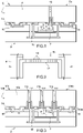
- a semiconductor device in particular a transducer designated by the number 1, comprises a substrate 2, a transduction microstructure 3 integrated in the substrate 2, and a cap 5.
- the transducer 1 is a pressure sensor
- the transduction microstructure 3 comprises an elastic transduction membrane 6 that closes a chamber 7 at reference pressure on one side.
- the semiconductor device may be a different type of transducer, such as, by way of non-limiting example, an electro-acoustic transducer (a microphone or a speaker) or a sensor for detecting gases or volatile substances; an actuator; or a microfluidic device comprising a microfluidic circuit and possibly microfluidic components, such as micropumps and microfluidic valves.
- the semiconductor device may be a so-called "Lab-On-Chip", which requires at least one inlet for introducing a biological specimen to be analysed and/or reagents into the microfluidic circuit from outside.
- the transduction microstructure does not necessarily have to comprise mobile or deformable parts.
- the transduction microstructure may comprise regions with fixed geometry obtained using materials with electrical properties that depend upon the concentration of the substances investigated.
- the face of the transduction membrane 6 opposite to the chamber 7 may be free or be coated with a passivation layer 8 and communicates with the external environment, as clarified in detail in what follows.
- the thickness and rigidity of the passivation layer 8 are in any case selected so as to enable deformation of the transduction membrane 6 as a result of pressure variations within a detection range.
- the transduction microstructure 3 is connected to the remaining part of the substrate 2 by elastic suspension elements 10.
- the cap 5 comprises a body 4 of semiconductor material, for example monocrystalline bulk silicon, and has a first face 5a adjacent to the substrate 2, to which it is joined, and a second face 5b facing outwards.
- the cap 5 has a thickness such as to offer mechanical protection to the transduction microstructure 3 and has a thickness, for example, comprised between 100 ⁇ m and 700 ⁇ m.
- Pedestals 11 extend from the first face 5a of the cap 5, are coated with respective coupling coatings 12, for example made of germanium, and are joined to respective bonding pads 13 of the substrate 2.
- the pedestals 11 have a height with respect to the first face 5a of the cap 5 such as to create a gap 14 between the cap 5, in particular the first face 5a, and the substrate 2.
- the height of the pedestals 11 may be comprised between 1 ⁇ m and 10 ⁇ m.
- the transduction microstructure 3 communicates with the gap 14.
- a channel 15 extends through the cap 5 from the second face 5b to the first face 5a.
- the channel 15 therefore has a first end open outwards and a second end open onto the gap 14 and communicating with the transduction microstructure 3.
- the channel 15 has a diameter selected according to design preferences and for example comprised between 10 ⁇ m and 30 ⁇ m.
- the cap 5 comprises a protective membrane 17 made of porous polycrystalline silicon and permeable to the aeriform substances, arranged across the channel 15.
- the protective membrane 17 may be located on the second face 5b of the cap 5 at the first end of the channel 15, or on the first face 5a of the cap 5 at the second end of the channel 15, or in an intermediate position along the channel 15 between the first end and the second end, as in the example of Figure 1 .
- the protective membrane 17 is part of a region 18 of porous polycrystalline silicon, which extends from the first face 5a of the cap 5 towards the inside of the channel 15 and coats the side surface of the channel 15 itself between the first face 5a and the protective membrane 17.
- the protective membrane 17 is released on both sides.
- the porosity of the protective membrane 17 is selected so as to withhold granular solid materials, dust and particulate and enable passage of aeriform substances.
- the pores 19 ( Figure 2 ) of the polycrystalline silicon forming the protective membrane 17 may have an equivalent diameter comprised between 5 nm and 50 nm.
- equivalent diameter here we mean the diameter of a duct having a circular section of passage and an area equal to the area of the mean section of passage of the pore.
- the pores 19, which in Figure 2 for simplicity are represented as rectilinear passages with constant section, extend in fact along generally curvilinear paths with variable cross-section.
- the dimensions and density of the pores 19 of the protective membrane 17 are such that the empty/full ratio is comprised between 5% and 30%, for example 10%. With these characteristics, the protective membrane 17 is able to withhold even drops of water. As a result of the surface tension, in fact, the drops of water are unable to penetrate into the pores 19 in the absence of a pressure difference applied between the two sides of the protective membrane 17.
- the packaged semiconductor transducer here designated by 100 comprises a plurality of channels 115, which extend through the cap 105 from the second face 105b to the first face 105a.
- Each channel 115 is provided with a respective protective membrane 117 made of polycrystalline silicon.
- the protective membranes 117 are portions of regions 118 of porous polycrystalline silicon and permeable to the aeriform substances, which extend from the second face 105b of the cap 105 towards the inside of the respective channels 115 and coat the side surface of the channels 115 themselves between the second face 105b and the protective membranes 117.
- the number, dimensions and position of the channels 115 are determined on the basis of the design preferences.
- the protective membrane 217 forms part of a region 218 of porous polycrystalline silicon, which extends from the second outer face 205b of the cap 205 towards the inside of the channel 215 and coats the side surface of the channel 215 itself between the second face 205b and the protective membrane 217.
- the packaged semiconductor transducer 1 of Figure 1 may be manufactured following the method described in what follows with reference to Figures 5-13 .
- the transduction microstructure 3 is obtained using a microstructure semiconductor wafer 2' (visible in Figure 14 ) according to a known method.
- a cap semiconductor wafer 5' which comprises a bulk layer 4' of monocrystalline silicon, is etched through a first resist structure 20a, defined with a first mask 20b, as illustrated in Figure 5 .
- the bulk layer 4' is removed for a thickness corresponding to the height of the pedestals 11, which are formed in regions protected by the first mask 20.
- the cap semiconductor wafer 5' is then again dry-etched with a second resist structure 21a (defined with a second mask 21b) to open a trench 23, as shown in Figure 6 .
- a second resist structure 21a defined with a second mask 21b
- an anisotropic dry etch is used, but equally a wet etch could be used, according to the design preferences.
- the stop layer 24 may be a layer of silicon oxide deposited or grown thermally. Alternatively, a different material may be used that may be etched in a selective way with respect to the polycrystalline silicon, such as a multilayer of silicon oxide and silicon nitride.
- the protection layer 25 is deposited on the stop layer 24 and may have a thickness comprised between 80 nm and 150 nm.
- the diameter of the pores and the empty/full ratio of the protective silicon layer 25 are selected on the basis of the design preferences for the protective membrane 17 described above.
- the protection layer 25 has pores of equivalent diameter comprised between 5 nm and 50 nm, the size and the density of the pores being such that the empty/full ratio is comprised between 5% and 30%.
- the stop layer 24 and the protection layer 25 coat in a conformable way the first face 5a of the cap semiconductor wafer 5', the side walls and the bottom of the trench 23.
- the portion of the protection layer 25 on the bottom of the trench 23 is to form the protective membrane 17.
- a resist structure 26a is deposited and defined via a third mask 26b so as to protect the inside of the trench 23, as illustrated in Figure 8 .
- the stop layer 24 and the protection layer 25 are selectively etched where they are not protected by the third resist structure 26a ( Figure 9 ).
- the region 18 of porous polycrystalline silicon is thus obtained, which is separated from the layer of monocrystalline bulk silicon of the cap semiconductor wafer 5' by a stop structure 24', defined by a residual portion of the stop layer 24.
- a fourth resist structure 29a is then deposited and defined via a fourth mask 29b ( Figure 11 ).
- the fourth resist structure 29a coats the pedestals 11 and the coupling layer 28 around them.
- the coupling layer 28 is selectively etched and removed where it is not protected by the fourth resist structure 29a.
- the coupling coatings 12 are thus created, as illustrated in Figure 12 .
- the cap semiconductor wafer 5' is turned upside down and etched on the back with a markedly anisotropic etch, for example a trench etch, in a position corresponding (i.e., aligned) to the trench 23, until the stop structure 24' is reached, which in this step protects the region 18 of porous polycrystalline silicon.
- the channel 15 is thus completed.
- the stop structure 24' is then selectively etched.
- the portion of the stop structure 24' exposed within the channel 15 is removed, thus releasing the protective membrane 17. Consequently, the protective membrane 17 extends in a direction transverse to a longitudinal axis of the channel 15 (i.e., an axis directed from the first end to the second end of the channel 15).
- the portions of the channel 15 on opposite sides of the protective membrane 17 communicate with one another through the protective membrane 17 of porous polycrystalline silicon.
- the cap semiconductor wafer 5' is finally joined to the bonding pads 13 of the microstructure semiconductor wafer 2' to form a composite wafer ( Figure 14 ), which is diced, thus obtaining a plurality of examples of the packaged semiconductor transducer 1 of Figure 1 .
- Each example comprises a portion of the microstructure semiconductor wafer 2', which defines the substrate 2 and contains the transduction microstructure 3, and a portion of the cap semiconductor wafer 5', which defines the cap 5.
- the method described may be immediately adapted by modifying the masks 21 and 26 and the trench etch on the back of the cap semiconductor wafer so as to open the desired number of channels instead of just one.
- the cap semiconductor wafer is turned upside down after the pedestals 11 have been formed.
- the machining operation proceeds on the back of the cap semiconductor wafer (second face 205b), as already described until the stop layer 24 and the protective silicon layer 25 are etched to form the region 218 of porous polycrystalline silicon and the stop structure 24'.
- the wafer is again turned over. Machining proceeds with formation and definition of the coupling layer on the first face 205a of the cap semiconductor wafer and with anisotropic etching of the bulk layer to form the channel 215, followed by selective removal of the stop layer within the channel 215.
- the cap semiconductor wafer is joined to the microstructure semiconductor wafer 2' and, after singulation of the composite wafer thus obtained, examples of the packaged semiconductor transducer 200 of Figure 4 are obtained.
- a packaged semiconductor transducer 300 is designated by number 300 and comprises the substrate 2, the transduction microstructure 3 integrated in the substrate 2 and a cap 305.
- the cap 305 comprises a bulk layer 304, a stop layer 324, a structural layer 341 and a protection layer 325 of porous polycrystalline silicon and permeable to aeriform substances.
- the stop layer 324 of silicon oxide, is interposed between the bulk layer 304, of monocrystalline silicon, and the structural layer 341, of a material that can be selectively etchable with respect to the structural layer 341, for example silicon nitride.
- Channels 315 extend from a second face 305b to a first face 305a of the cap 305 through the bulk layer 304, the stop layer 324, and the structural layer 341.
- the protection layer 325 forms protective membranes 317 in the channels 315. More precisely, the protection layer 325, which covers the first face 305a of the cap 305, penetrates into the channels 315 coating the side surfaces substantially as far as an interface 343 between the structural layer 341 and the stop layer 324. At the depth of the interface 343, the protection layer 325 extends in a direction transverse to longitudinal axes of the channels 315 to form the protective membranes 317.
- the first face 305a of the cap 305 is joined to the substrate 2 by pedestals 311 that act as adhesion structures and, at the same time, have a height such as to create a gap 314 between the substrate 2 and the cap 305.
- the microstructure 3 communicates with the outside through the channels 315 and the protective membranes 317, which enable passage of aeriform substances.
- a cap semiconductor wafer 305' initially comprises the bulk layer 304.
- the stop layer 324 and the structural layer 341 are formed in succession on the bulk layer 304 ( Figure 16 ).
- the structural layer 341 is then selectively etched using a mask 320 for opening cavities 345, which extend as far as the stop layer 324, as illustrated in Figure 17 .
- the protection layer 325 is then formed on the first face 305a of the cap semiconductor wafer 305' ( Figure 18 ), which is then turned upside down and etched on the back, i.e., on the side of the second face 305b, in positions corresponding (aligned) to respective cavities 345 ( Figure 19 ).
- a markedly anisotropic trench etch is first carried out as far as the stop layer 324, and then the stop layer 324 is etched where it is left exposed. In this way, the protective membranes 317 are freed and the channels 315 are completed.
- the protection layer 325 is selectively etched to expose the structural layer 341 where the pedestals 311 are then formed.
- the cap semiconductor wafer 305' is finally joined to the bonding pads 13 of the microstructure semiconductor wafer 2' to form a composite wafer, which is then diced, thus obtaining a plurality of examples of the packaged semiconductor transducer 300 of Figure 15 .
- Each example comprises a portion of the microstructure semiconductor wafer 2', which defines the substrate 2 and contains the transduction microstructure 3, and a portion of the cap semiconductor wafer 305', which defines the cap 305.
- the presence of the protective membrane through the channel or channels prevents any contamination of the transduction microstructure with particulate and dust within the device, without jeopardizing the fluidic connection with the outside world, in particular for aeriform substances.
- the protective membrane prevents or at least hinders entry of small amounts of liquid, for example due to exposure to splashes or to the use during sports activity.
- the diameter of the pores of the protective membrane is sufficient to prevent entry of drops as a result of the surface tension.
- the transduction microstructure albeit remaining protected from contaminating agents, is in any case adequately exposed and coupled to the quantities to be detected (pressure, substances, etc.) thanks to the porosity of the protective membrane.
- the constraints on the minimum diameter of the channel may even be at least in part relaxed because the barrier effect against contaminating agents is performed effectively by the protective membrane. Therefore, the presence of the protective membrane also affords a greater flexibility in design of the cap.
- the use of the stop layer between the layer of porous polycrystalline silicon and the bulk layer enables definition and release of the protective membrane within the channels in a simple way during machining at the wafer level. Operations for applying polymeric membranes at the device level following upon singulation can thus be avoided, with considerable reduction in costs.
- the stop layer and the layer of porous polycrystalline silicon may be formed with standard techniques of machining of semiconductors and therefore in a reliable and inexpensive way.
- the characteristics of the protective membrane, such as porosity and thickness, may be easily controlled.
- Figure 20 shows an electronic system 400 that may be of any type, in particular, but not exclusively, a wearable device, such as a watch, a bracelet, or a smart band; a computer, such as a mainframe, a personal computer, a laptop or a tablet; a smartphone; a digital music player, a digital camera or any other device designed to process, store, transmit or receive information.
- the electronic device 1 may be a general-purpose or embedded processing system in a device, an apparatus or a further system.
- the electronic system 400 comprises a processing unit 402, memory devices 403, a packaged semiconductor transducer, for example the packaged semiconductor transducer 1 of Figure 1 , and may moreover be provided with input/output (I/O) devices 405 (for example a keyboard, a mouse or a touchscreen), a wireless interface 406, peripherals 407.1, ..., 407.N and possibly further auxiliary devices (here not illustrated).
- I/O input/output
- the components of the electronic system 400 may be coupled in communication with one another directly and/or indirectly through a bus 408.
- the electronic system 400 may moreover comprise a battery 409. It should be noted that the scope of the present invention is not limited to embodiments necessarily having one or all of the devices listed.
- the processing unit 402 may for example comprise one or more microprocessors, microcontrollers, and the like, according to the design preferences.
- the memory devices 403 may comprise volatile memory devices and non-volatile memory devices of various kinds, for example SRAMs and/or DRAMs for volatile and solid-state memories, magnetic disks and/or optical disks for non-volatile memories.
Landscapes
- Engineering & Computer Science (AREA)
- Microelectronics & Electronic Packaging (AREA)
- Manufacturing & Machinery (AREA)
- Computer Hardware Design (AREA)
- Micromachines (AREA)
- Pressure Sensors (AREA)
Abstract
Description
- The present invention relates to a semiconductor device and to a method for manufacturing a semiconductor device.
- As is known, electronic, microelectromechanical and microfluidic devices must be protected against external agents, such as dust, moisture and aggressive substances, which may cause damage and malfunctioning. In many cases, the devices may be sealed within packages that isolate them completely from the external environment from the mechanical and fluidic standpoint, while enabling electrical or electromagnetic coupling. However, devices exist, in particular some transducers, that by their very nature require a connection not only electrical with the outside world and consequently cannot benefit from sealed packages. For instance, electro-acoustic transducers (microphones and speakers), pressure sensors and sensors for detecting gases or volatile substances must be fluidically coupled to the environment for receiving and/or transmitting static pressures or pressure variations, according to the type of device and the operating principle. The packages for these devices are therefore provided with openings, which if, on the one hand, guarantee proper operation, on the other, reduce protection against penetration of potentially harmful external agents. Other examples of devices that cannot be sealed are some types of actuators and many microfluidic circuits and devices, such as micropumps and microfluidic valves.
- Known solutions envisage either closing the openings by applying layers of transpirant polymeric fabric (for example, expanded polytetrafluoroethylene, ePTFE) or providing openings in the form of channels or vents having a very small cross-section so as to prevent entry of particulate and dust above a given diameter. However, both solutions have limitations. In the first case, applying layers of fabric entails considerable costs, because the operation can be carried out only by pick and place on the individual device and not during machining at the wafer level. The channels or vents may be provided during manufacture at the wafer level, but, given that to provide an adequate mechanical protection the packages normally have a considerable thickness, it may be difficult to reduce the diameter of the channels until the desired protection is guaranteed. Consequently, fine particulate could reach the device to be protected.
- The aim of the present invention is to provide a semiconductor device and a method for manufacturing a semiconductor device that will enable the limitations described to be overcome or at least attenuated.
- According to the present invention a semiconductor device and a method for manufacturing a semiconductor device are provided, as defined in
claims - For a better understanding of the invention, some embodiments thereof will now be described, purely by way of non-limiting example and with reference to the attached drawings, wherein:
-
Figure 1 is a cross-sectional view through a semiconductor device according to an embodiment of the present invention; -
Figure 2 shows an enlarged detail of the device ofFigure 1 ; -
Figure 3 is a cross-sectional view through a semiconductor device according to a different embodiment of the present invention; -
Figure 4 is a cross-sectional view through a semiconductor device according to a further embodiment of the present invention; -
Figures 5-14 show a semiconductor wafer in successive machining steps of a process for manufacturing a semiconductor device according to one embodiment of the present invention; -
Figure 15 is a cross-sectional view through a semiconductor device according to another embodiment of the present invention; -
Figures 16-19 show a semiconductor wafer in successive machining steps of a process for manufacturing a semiconductor device according to a different embodiment of the present invention; and -
Figure 20 is a simplified block diagram of an electronic system incorporating a semiconductor device according to the present invention. - With reference to
Figure 1 , a semiconductor device according to an embodiment of the present invention, in particular a transducer designated by thenumber 1, comprises asubstrate 2, atransduction microstructure 3 integrated in thesubstrate 2, and acap 5. In the example illustrated, thetransducer 1 is a pressure sensor, and thetransduction microstructure 3 comprises anelastic transduction membrane 6 that closes achamber 7 at reference pressure on one side. In other embodiments not illustrated, the semiconductor device may be a different type of transducer, such as, by way of non-limiting example, an electro-acoustic transducer (a microphone or a speaker) or a sensor for detecting gases or volatile substances; an actuator; or a microfluidic device comprising a microfluidic circuit and possibly microfluidic components, such as micropumps and microfluidic valves. For instance, the semiconductor device may be a so-called "Lab-On-Chip", which requires at least one inlet for introducing a biological specimen to be analysed and/or reagents into the microfluidic circuit from outside. Furthermore, it is understood that the transduction microstructure does not necessarily have to comprise mobile or deformable parts. For instance, in a sensor of volatile substances the transduction microstructure may comprise regions with fixed geometry obtained using materials with electrical properties that depend upon the concentration of the substances investigated. - The face of the
transduction membrane 6 opposite to thechamber 7 may be free or be coated with apassivation layer 8 and communicates with the external environment, as clarified in detail in what follows. The thickness and rigidity of thepassivation layer 8 are in any case selected so as to enable deformation of thetransduction membrane 6 as a result of pressure variations within a detection range. - In an embodiment, the
transduction microstructure 3 is connected to the remaining part of thesubstrate 2 byelastic suspension elements 10. - The
cap 5 comprises abody 4 of semiconductor material, for example monocrystalline bulk silicon, and has afirst face 5a adjacent to thesubstrate 2, to which it is joined, and asecond face 5b facing outwards. Thecap 5 has a thickness such as to offer mechanical protection to thetransduction microstructure 3 and has a thickness, for example, comprised between 100 µm and 700 µm. -
Pedestals 11 extend from thefirst face 5a of thecap 5, are coated withrespective coupling coatings 12, for example made of germanium, and are joined torespective bonding pads 13 of thesubstrate 2. Thepedestals 11 have a height with respect to thefirst face 5a of thecap 5 such as to create agap 14 between thecap 5, in particular thefirst face 5a, and thesubstrate 2. For instance, the height of thepedestals 11 may be comprised between 1 µm and 10 µm. Thetransduction microstructure 3 communicates with thegap 14. - In the embodiment of
Figure 1 , achannel 15 extends through thecap 5 from thesecond face 5b to thefirst face 5a. Thechannel 15 therefore has a first end open outwards and a second end open onto thegap 14 and communicating with thetransduction microstructure 3. Thechannel 15 has a diameter selected according to design preferences and for example comprised between 10 µm and 30 µm. - As illustrated in greater detail in
Figure 2 , thecap 5 comprises aprotective membrane 17 made of porous polycrystalline silicon and permeable to the aeriform substances, arranged across thechannel 15. It is understood that theprotective membrane 17 may be located on thesecond face 5b of thecap 5 at the first end of thechannel 15, or on thefirst face 5a of thecap 5 at the second end of thechannel 15, or in an intermediate position along thechannel 15 between the first end and the second end, as in the example ofFigure 1 . In particular, theprotective membrane 17 is part of aregion 18 of porous polycrystalline silicon, which extends from thefirst face 5a of thecap 5 towards the inside of thechannel 15 and coats the side surface of thechannel 15 itself between thefirst face 5a and theprotective membrane 17. In one embodiment, theprotective membrane 17 is released on both sides. - The porosity of the
protective membrane 17 is selected so as to withhold granular solid materials, dust and particulate and enable passage of aeriform substances. In one embodiment, the pores 19 (Figure 2 ) of the polycrystalline silicon forming theprotective membrane 17 may have an equivalent diameter comprised between 5 nm and 50 nm. By "equivalent diameter" here we mean the diameter of a duct having a circular section of passage and an area equal to the area of the mean section of passage of the pore. Thepores 19, which inFigure 2 for simplicity are represented as rectilinear passages with constant section, extend in fact along generally curvilinear paths with variable cross-section. Moreover, the dimensions and density of thepores 19 of theprotective membrane 17 are such that the empty/full ratio is comprised between 5% and 30%, for example 10%. With these characteristics, theprotective membrane 17 is able to withhold even drops of water. As a result of the surface tension, in fact, the drops of water are unable to penetrate into thepores 19 in the absence of a pressure difference applied between the two sides of theprotective membrane 17. - With reference to
Figure 3 , in one embodiment the packaged semiconductor transducer here designated by 100, comprises a plurality ofchannels 115, which extend through thecap 105 from thesecond face 105b to thefirst face 105a. Eachchannel 115 is provided with a respectiveprotective membrane 117 made of polycrystalline silicon. Theprotective membranes 117 are portions ofregions 118 of porous polycrystalline silicon and permeable to the aeriform substances, which extend from thesecond face 105b of thecap 105 towards the inside of therespective channels 115 and coat the side surface of thechannels 115 themselves between thesecond face 105b and theprotective membranes 117. The number, dimensions and position of thechannels 115 are determined on the basis of the design preferences. - In the embodiment illustrated in
Figure 4 , in a packagedsemiconductor transducer 200 theprotective membrane 217 forms part of aregion 218 of porous polycrystalline silicon, which extends from the secondouter face 205b of thecap 205 towards the inside of thechannel 215 and coats the side surface of thechannel 215 itself between thesecond face 205b and theprotective membrane 217. - The packaged
semiconductor transducer 1 ofFigure 1 may be manufactured following the method described in what follows with reference toFigures 5-13 . - The
transduction microstructure 3 is obtained using a microstructure semiconductor wafer 2' (visible inFigure 14 ) according to a known method. - To manufacture the
cap 5 ofFigure 1 , a cap semiconductor wafer 5', which comprises a bulk layer 4' of monocrystalline silicon, is etched through afirst resist structure 20a, defined with afirst mask 20b, as illustrated inFigure 5 . The bulk layer 4' is removed for a thickness corresponding to the height of thepedestals 11, which are formed in regions protected by the first mask 20. - The cap semiconductor wafer 5' is then again dry-etched with a
second resist structure 21a (defined with asecond mask 21b) to open atrench 23, as shown inFigure 6 . In the example here illustrated, an anisotropic dry etch is used, but equally a wet etch could be used, according to the design preferences. - Then (
Figure 7 ), astop layer 24 and aprotection layer 25 of porous polycrystalline silicon and permeable to aeriform substances, are formed in succession on the cap semiconductor wafer 5', both on thefirst face 5a and inside thetrench 23. Thestop layer 24 may be a layer of silicon oxide deposited or grown thermally. Alternatively, a different material may be used that may be etched in a selective way with respect to the polycrystalline silicon, such as a multilayer of silicon oxide and silicon nitride. Theprotection layer 25 is deposited on thestop layer 24 and may have a thickness comprised between 80 nm and 150 nm. In addition, the diameter of the pores and the empty/full ratio of theprotective silicon layer 25 are selected on the basis of the design preferences for theprotective membrane 17 described above. For instance, theprotection layer 25 has pores of equivalent diameter comprised between 5 nm and 50 nm, the size and the density of the pores being such that the empty/full ratio is comprised between 5% and 30%. - The
stop layer 24 and theprotection layer 25 coat in a conformable way thefirst face 5a of the cap semiconductor wafer 5', the side walls and the bottom of thetrench 23. The portion of theprotection layer 25 on the bottom of thetrench 23 is to form theprotective membrane 17. - After the
stop layer 24 and theprotection layer 25 have been formed, a resiststructure 26a is deposited and defined via athird mask 26b so as to protect the inside of thetrench 23, as illustrated inFigure 8 . Thestop layer 24 and theprotection layer 25 are selectively etched where they are not protected by the third resiststructure 26a (Figure 9 ). Theregion 18 of porous polycrystalline silicon is thus obtained, which is separated from the layer of monocrystalline bulk silicon of the cap semiconductor wafer 5' by a stop structure 24', defined by a residual portion of thestop layer 24. - After the third resist
structure 26a has been removed, acoupling layer 28, for example, of germanium, is deposited in a conformable way on the cap semiconductor wafer 5' (Figure 10 ). - A fourth resist
structure 29a is then deposited and defined via afourth mask 29b (Figure 11 ). The fourth resiststructure 29a coats thepedestals 11 and thecoupling layer 28 around them. Thecoupling layer 28 is selectively etched and removed where it is not protected by the fourth resiststructure 29a. Thecoupling coatings 12 are thus created, as illustrated inFigure 12 . - With reference to
Figure 13 , the cap semiconductor wafer 5' is turned upside down and etched on the back with a markedly anisotropic etch, for example a trench etch, in a position corresponding (i.e., aligned) to thetrench 23, until the stop structure 24' is reached, which in this step protects theregion 18 of porous polycrystalline silicon. Thechannel 15 is thus completed. The stop structure 24' is then selectively etched. In particular, the portion of the stop structure 24' exposed within thechannel 15 is removed, thus releasing theprotective membrane 17. Consequently, theprotective membrane 17 extends in a direction transverse to a longitudinal axis of the channel 15 (i.e., an axis directed from the first end to the second end of the channel 15). The portions of thechannel 15 on opposite sides of theprotective membrane 17 communicate with one another through theprotective membrane 17 of porous polycrystalline silicon. - The cap semiconductor wafer 5' is finally joined to the
bonding pads 13 of the microstructure semiconductor wafer 2' to form a composite wafer (Figure 14 ), which is diced, thus obtaining a plurality of examples of the packagedsemiconductor transducer 1 ofFigure 1 . Each example comprises a portion of the microstructure semiconductor wafer 2', which defines thesubstrate 2 and contains thetransduction microstructure 3, and a portion of the cap semiconductor wafer 5', which defines thecap 5. - In order to manufacture the packaged
semiconductor transducer 100 ofFigure 3 , the method described may be immediately adapted by modifying the masks 21 and 26 and the trench etch on the back of the cap semiconductor wafer so as to open the desired number of channels instead of just one. - In order to manufacture the packaged
semiconductor transducer 200 ofFigure 4 , instead, the cap semiconductor wafer is turned upside down after thepedestals 11 have been formed. The machining operation proceeds on the back of the cap semiconductor wafer (second face 205b), as already described until thestop layer 24 and theprotective silicon layer 25 are etched to form theregion 218 of porous polycrystalline silicon and the stop structure 24'. Before depositing the germanium coupling layer, the wafer is again turned over. Machining proceeds with formation and definition of the coupling layer on thefirst face 205a of the cap semiconductor wafer and with anisotropic etching of the bulk layer to form thechannel 215, followed by selective removal of the stop layer within thechannel 215. The cap semiconductor wafer is joined to the microstructure semiconductor wafer 2' and, after singulation of the composite wafer thus obtained, examples of the packagedsemiconductor transducer 200 ofFigure 4 are obtained. - With reference to
Figure 15 , a packagedsemiconductor transducer 300 according to an embodiment of the present invention is designated bynumber 300 and comprises thesubstrate 2, thetransduction microstructure 3 integrated in thesubstrate 2 and acap 305. - The
cap 305 comprises abulk layer 304, astop layer 324, astructural layer 341 and aprotection layer 325 of porous polycrystalline silicon and permeable to aeriform substances. Thestop layer 324, of silicon oxide, is interposed between thebulk layer 304, of monocrystalline silicon, and thestructural layer 341, of a material that can be selectively etchable with respect to thestructural layer 341, for example silicon nitride. -
Channels 315 extend from asecond face 305b to afirst face 305a of thecap 305 through thebulk layer 304, thestop layer 324, and thestructural layer 341. Theprotection layer 325 formsprotective membranes 317 in thechannels 315. More precisely, theprotection layer 325, which covers thefirst face 305a of thecap 305, penetrates into thechannels 315 coating the side surfaces substantially as far as aninterface 343 between thestructural layer 341 and thestop layer 324. At the depth of theinterface 343, theprotection layer 325 extends in a direction transverse to longitudinal axes of thechannels 315 to form theprotective membranes 317. - The
first face 305a of thecap 305 is joined to thesubstrate 2 bypedestals 311 that act as adhesion structures and, at the same time, have a height such as to create agap 314 between thesubstrate 2 and thecap 305. - The
microstructure 3 communicates with the outside through thechannels 315 and theprotective membranes 317, which enable passage of aeriform substances. - Whereas the
transduction microstructure 3 is obtained using a microstructure semiconductor wafer 2' as already described, according to a method for manufacturing the packagedsemiconductor transducer 300 ofFigure 15 illustrated inFigures 16-19 , a cap semiconductor wafer 305' initially comprises thebulk layer 304. Thestop layer 324 and thestructural layer 341 are formed in succession on the bulk layer 304 (Figure 16 ). - The
structural layer 341 is then selectively etched using amask 320 for openingcavities 345, which extend as far as thestop layer 324, as illustrated inFigure 17 . - The
protection layer 325 is then formed on thefirst face 305a of the cap semiconductor wafer 305' (Figure 18 ), which is then turned upside down and etched on the back, i.e., on the side of thesecond face 305b, in positions corresponding (aligned) to respective cavities 345 (Figure 19 ). In particular, a markedly anisotropic trench etch is first carried out as far as thestop layer 324, and then thestop layer 324 is etched where it is left exposed. In this way, theprotective membranes 317 are freed and thechannels 315 are completed. - The
protection layer 325 is selectively etched to expose thestructural layer 341 where thepedestals 311 are then formed. - The cap semiconductor wafer 305' is finally joined to the
bonding pads 13 of the microstructure semiconductor wafer 2' to form a composite wafer, which is then diced, thus obtaining a plurality of examples of the packagedsemiconductor transducer 300 ofFigure 15 . Each example comprises a portion of the microstructure semiconductor wafer 2', which defines thesubstrate 2 and contains thetransduction microstructure 3, and a portion of the cap semiconductor wafer 305', which defines thecap 305. - The invention described presents various advantages. From the structural standpoint, the presence of the protective membrane through the channel or channels prevents any contamination of the transduction microstructure with particulate and dust within the device, without jeopardizing the fluidic connection with the outside world, in particular for aeriform substances. Furthermore, the protective membrane prevents or at least hinders entry of small amounts of liquid, for example due to exposure to splashes or to the use during sports activity. In the case of water, for example, the diameter of the pores of the protective membrane is sufficient to prevent entry of drops as a result of the surface tension.
- Proper operation of the transducer is ensured because the transduction microstructure, albeit remaining protected from contaminating agents, is in any case adequately exposed and coupled to the quantities to be detected (pressure, substances, etc.) thanks to the porosity of the protective membrane. Indeed, the constraints on the minimum diameter of the channel may even be at least in part relaxed because the barrier effect against contaminating agents is performed effectively by the protective membrane. Therefore, the presence of the protective membrane also affords a greater flexibility in design of the cap.
- As regards the manufacturing method, the use of the stop layer between the layer of porous polycrystalline silicon and the bulk layer enables definition and release of the protective membrane within the channels in a simple way during machining at the wafer level. Operations for applying polymeric membranes at the device level following upon singulation can thus be avoided, with considerable reduction in costs. Moreover, the stop layer and the layer of porous polycrystalline silicon may be formed with standard techniques of machining of semiconductors and therefore in a reliable and inexpensive way. Also the characteristics of the protective membrane, such as porosity and thickness, may be easily controlled.
- Etching of the bulk layer on both sides, before opening the trench on one side and then with anisotropic etching on the opposite side, makes it possible to obtain extreme shape ratios through the channel that traverses the cap. Furthermore, the channels can be formed without any need to thin the bulk layer of the cap wafer and therefore without degrading the mechanical resistance thereof. This adds flexibility to the design and to manufacturing of semiconductor transducers.
-
Figure 20 shows anelectronic system 400 that may be of any type, in particular, but not exclusively, a wearable device, such as a watch, a bracelet, or a smart band; a computer, such as a mainframe, a personal computer, a laptop or a tablet; a smartphone; a digital music player, a digital camera or any other device designed to process, store, transmit or receive information. Theelectronic device 1 may be a general-purpose or embedded processing system in a device, an apparatus or a further system. - The
electronic system 400 comprises aprocessing unit 402,memory devices 403, a packaged semiconductor transducer, for example the packagedsemiconductor transducer 1 ofFigure 1 , and may moreover be provided with input/output (I/O) devices 405 (for example a keyboard, a mouse or a touchscreen), awireless interface 406, peripherals 407.1, ..., 407.N and possibly further auxiliary devices (here not illustrated). The components of theelectronic system 400 may be coupled in communication with one another directly and/or indirectly through abus 408. Theelectronic system 400 may moreover comprise abattery 409. It should be noted that the scope of the present invention is not limited to embodiments necessarily having one or all of the devices listed. - The
processing unit 402 may for example comprise one or more microprocessors, microcontrollers, and the like, according to the design preferences. - The
memory devices 403 may comprise volatile memory devices and non-volatile memory devices of various kinds, for example SRAMs and/or DRAMs for volatile and solid-state memories, magnetic disks and/or optical disks for non-volatile memories. - Finally, it is evident that modifications and variations may be made to the device and to the method described, without thereby departing from the scope of the present invention, as defined in the annexed claims.
Claims (16)
- A semiconductor device comprising:a substrate (2);a transduction microstructure (3) integrated in the substrate (2);a cap (5; 105; 205; 305) joined to the substrate (2) and having a first face (5a; 105a; 205a; 305a) adjacent to the substrate (2) and an outer second face (5b; 105b; 205b; 305b);a channel (15; 115; 315) extending through the cap (5; 105; 205; 305) from the second face (5b; 105b; 205b; 305b) to the first face (5a; 105a; 205a; 305a) and communicating with the transduction microstructure (3);a protective membrane (17; 117; 217; 317) made of porous polycrystalline silicon and permeable to aeriform substances, the protective membrane (17; 117; 217; 317) being arranged across the channel (15; 115; 315).
- The device according to claim 1, wherein the protective membrane (17; 117; 217; 317) is located along the channel (15; 115; 315) at an intermediate position between the second face (5b; 105b; 205b; 305b) and the first face (5a; 105a; 205a; 305a).
- The device according to claim 1 or 2, wherein the protective membrane (17; 117; 217; 317) has pores (19) with an equivalent diameter comprised between 5 nm and 50 nm.
- The device according to any one of the preceding claims, wherein a gap (14) is defined between the first face (5a; 105a; 205a; 305a) of the cap (5; 105; 205; 305) and the substrate (2) and wherein the transduction microstructure (3) and the channel (15; 115; 315) communicate with the gap (14) .
- The device according to any one of the preceding claims, comprising a region (18; 118; 218) of porous polycrystalline silicon that coats a side surface of the channel (15; 115; 215) between the protective membrane (17; 117; 218) and one between the first face (5a; 105a) and the second face (205a), wherein the protective membrane (17) is part of the region (18; 118; 218) of porous polycrystalline silicon.
- The device according to any one of the preceding claims, comprising a plurality of channels (115; 315) and a plurality of protective membranes (117; 317) of porous polycrystalline silicon and permeable to aeriform substances, each protective membrane (17; 117; 217; 317) being arranged across a respective one of the channels (115; 315) .
- An electronic system comprising a processing unit (402) and a semiconductor device (1; 100; 200; 300) according to any one of the preceding claims.
- A method for manufacturing a semiconductor device, comprising:forming a transduction microstructure (3) in a microstructure semiconductor wafer (2');forming a stop layer (24; 324) on a bulk layer (4'; 304') of a cap semiconductor wafer (5'; 305');forming a protection layer (25; 325) made of porous polycrystalline silicon and permeable to aeriform substances at least in part on the stop layer (24; 324);forming a channel (15; 115; 315) through the cap semiconductor wafer (5'; 305') from a first face (5a; 105a; 205a; 305a) to a second face (5b; 105b; 205b; 305b) thereof, wherein forming the channel (15; 115; 315) comprises etching in an anisotropic way the bulk layer (4'; 304') as far as the stop layer (24; 324) on one side of the cap semiconductor wafer (5'; 305') opposite to the protection layer (25; 325);removing the stop layer (24; 324) inside the channel (15; 315); andjoining the cap (5; 105; 205; 305) to the microstructure semiconductor wafer (2') so that the channel (15; 115; 315) will communicate with the transduction microstructure (3).
- The method according to claim 8, wherein forming the channel (15; 315) comprises forming a depression (23; 345) in the cap semiconductor wafer (5'; 305') and wherein forming the protection layer (25; 325) comprises depositing the protection layer (25; 325) within the depression (23; 345).
- The method according to claim 9, wherein forming the depression (23) comprises opening a trench in the bulk layer (4').
- The method according to claim 9, wherein forming the depression (345) comprises depositing a structural layer (341) on the stop layer (324) and selectively etching the structural layer (341).
- The method according to any one of claims 9 to 11, wherein forming the protection layer (25; 325) comprises depositing the protection layer (25; 325) directly in contact with the stop layer in the depression (23; 345).
- The method according to any one of claims 9 to 12, wherein the protection layer (25; 325) has pores (19) with an equivalent diameter comprised between 5 nm and 50 nm and wherein the dimensions and density of the pores (19) are such that an empty/full ratio of the protection layer (25; 325) is comprised between 5% and 30%.
- The method according to any one of claims 8 to 13, wherein forming the channel (15; 115; 315) comprises etching in an anisotropic way the bulk layer (4'; 304') in a position corresponding to the depression (23; 45).
- The method according to any one of claims 8 to 14, comprising forming a plurality of channels (115; 315) through the cap semiconductor wafer (5'; 305') from the first face (5a; 105a; 205a; 305a) to the second face (5b; 105b; 205b; 305b) thereof.
- The method according to any one of claims 8 to 15, comprising:forming pedestals (11) extending from the first face (5a; 105a; 205a; 305a) of the cap semiconductor wafer (5'; 305'); andforming coupling coatings (12) on the pedestals (11);wherein joining the cap semiconductor wafer (5'; 305') to the microstructure semiconductor wafer (2') comprises joining the pedestals (11) to the microstructure semiconductor wafer (2');wherein the pedestals (11) have a height with respect to the first face (5a; 105a; 205a; 305a) of the cap semiconductor wafer (5'; 305') such as to create a gap (14) between the first face (5a; 105a; 205a; 305a) and the microstructure semiconductor wafer (2') of the substrate (2) ;and wherein the transduction microstructure (3) and the channel (15; 115; 315) communicate with the gap (14).
Applications Claiming Priority (1)
| Application Number | Priority Date | Filing Date | Title |
|---|---|---|---|
| IT202000029078 | 2020-11-30 |
Publications (2)
| Publication Number | Publication Date |
|---|---|
| EP4005972A1 true EP4005972A1 (en) | 2022-06-01 |
| EP4005972B1 EP4005972B1 (en) | 2024-11-20 |
Family
ID=74347655
Family Applications (1)
| Application Number | Title | Priority Date | Filing Date |
|---|---|---|---|
| EP21211139.7A Active EP4005972B1 (en) | 2020-11-30 | 2021-11-29 | Semiconductor device and method for manufacturing a semiconductor device |
Country Status (3)
| Country | Link |
|---|---|
| US (1) | US12134556B2 (en) |
| EP (1) | EP4005972B1 (en) |
| CN (2) | CN216946212U (en) |
Families Citing this family (3)
| Publication number | Priority date | Publication date | Assignee | Title |
|---|---|---|---|---|
| US12134556B2 (en) * | 2020-11-30 | 2024-11-05 | Stmicroelectronics S.R.L. | Semiconductor device and method for manufacturing a semiconductor device |
| CN115499587B (en) * | 2022-09-15 | 2024-10-18 | 苏州云昕智能科技有限公司 | Camera module focusing device based on machine vision |
| DE102023207112A1 (en) * | 2023-07-26 | 2025-01-30 | Robert Bosch Gesellschaft mit beschränkter Haftung | Method for producing a microelectromechanical device and microelectromechanical device |
Citations (3)
| Publication number | Priority date | Publication date | Assignee | Title |
|---|---|---|---|---|
| US8536663B1 (en) * | 2011-04-28 | 2013-09-17 | Amkor Technology, Inc. | Metal mesh lid MEMS package and method |
| US20180070162A1 (en) * | 2015-05-14 | 2018-03-08 | Knowles Electronics, Llc | Sensor device with ingress protection |
| US20180103324A1 (en) * | 2016-10-06 | 2018-04-12 | Hyundai Motor Company | Microphone and manufacturing method thereof |
Family Cites Families (10)
| Publication number | Priority date | Publication date | Assignee | Title |
|---|---|---|---|---|
| US5919364A (en) | 1996-06-24 | 1999-07-06 | Regents Of The University Of California | Microfabricated filter and shell constructed with a permeable membrane |
| US7075160B2 (en) | 2003-06-04 | 2006-07-11 | Robert Bosch Gmbh | Microelectromechanical systems and devices having thin film encapsulated mechanical structures |
| JP5174673B2 (en) * | 2005-10-14 | 2013-04-03 | エスティーマイクロエレクトロニクス エス.アール.エル. | Electronic device with substrate level assembly and method of manufacturing the same |
| ITTO20090616A1 (en) * | 2009-08-05 | 2011-02-06 | St Microelectronics Srl | PROCESS OF MANUFACTURING OF MEMS DEVICES EQUIPPED WITH CUTTED CAVITIES AND MEMS DEVICE SO OBTAINED |
| KR101332701B1 (en) * | 2010-09-20 | 2013-11-25 | 페어차일드 세미컨덕터 코포레이션 | Microelectromechanical pressure sensor including reference capacitor |
| EP2465817B1 (en) * | 2010-12-16 | 2016-03-30 | Nxp B.V. | Method for encapsulating a MEMS structure |
| ITUA20163571A1 (en) * | 2016-05-18 | 2017-11-18 | St Microelectronics Srl | MEMS ACOUSTIC TRANSDUCER WITH INTERDIGATED ELECTRODES AND ITS MANUFACTURING PROCEDURE |
| IT201600121533A1 (en) * | 2016-11-30 | 2018-05-30 | St Microelectronics Srl | MEMS INTEGRATED ELECTROACOUSTIC TRANSDUCER WITH IMPROVED SENSITIVITY AND RELATIVE PROCESS OF MANUFACTURING |
| IT201800006160A1 (en) * | 2018-06-08 | 2019-12-08 | PROCEDURE FOR MANUFACTURING A MICROELECTROMECHANICAL DEVICE WITH A SUSPENDED BURIED STRUCTURE AND RELATED MICROELECTROMECHANICAL DEVICE | |
| US12134556B2 (en) * | 2020-11-30 | 2024-11-05 | Stmicroelectronics S.R.L. | Semiconductor device and method for manufacturing a semiconductor device |
-
2021
- 2021-11-23 US US17/534,286 patent/US12134556B2/en active Active
- 2021-11-29 CN CN202122952681.XU patent/CN216946212U/en not_active Withdrawn - After Issue
- 2021-11-29 CN CN202111430582.3A patent/CN114572928B/en active Active
- 2021-11-29 EP EP21211139.7A patent/EP4005972B1/en active Active
Patent Citations (3)
| Publication number | Priority date | Publication date | Assignee | Title |
|---|---|---|---|---|
| US8536663B1 (en) * | 2011-04-28 | 2013-09-17 | Amkor Technology, Inc. | Metal mesh lid MEMS package and method |
| US20180070162A1 (en) * | 2015-05-14 | 2018-03-08 | Knowles Electronics, Llc | Sensor device with ingress protection |
| US20180103324A1 (en) * | 2016-10-06 | 2018-04-12 | Hyundai Motor Company | Microphone and manufacturing method thereof |
Also Published As
| Publication number | Publication date |
|---|---|
| CN216946212U (en) | 2022-07-12 |
| EP4005972B1 (en) | 2024-11-20 |
| US12134556B2 (en) | 2024-11-05 |
| CN114572928B (en) | 2026-01-02 |
| US20220169498A1 (en) | 2022-06-02 |
| CN114572928A (en) | 2022-06-03 |
Similar Documents
| Publication | Publication Date | Title |
|---|---|---|
| EP4005972B1 (en) | Semiconductor device and method for manufacturing a semiconductor device | |
| US20220212920A1 (en) | Liquid-resistant air inlet passive device and methods of making same | |
| TWI711575B (en) | Mems devices and processes | |
| CN101631739B (en) | Method for manufacturing MEMS microphone | |
| US10183860B2 (en) | Method to package multiple mems sensors and actuators at different gases and cavity pressures | |
| US9340414B2 (en) | Method and structure of monolithically integrated absolute pressure sensor | |
| CN111051839B (en) | Micromechanical sensor device and corresponding production method | |
| US8685776B2 (en) | Wafer level packaged MEMS device | |
| CN111108758B (en) | MEMS microphone system | |
| CN101331080A (en) | Substrate-level components for integrated devices, their manufacturing processes, and related integrated devices | |
| US20150292973A1 (en) | Humidity resistant sensors and methods of making same | |
| CN112897454B (en) | MEMS device and method of manufacturing the same | |
| US20160229687A1 (en) | Chip package and fabrication method thereof | |
| CN111246355B (en) | MEMS devices and methods of forming MEMS devices | |
| US20240182295A1 (en) | Pressure transducer device with hybrid barrier structure and method for manufacturing same | |
| US10684185B2 (en) | Sensor and/or sound detection device and manufacturing method for a sensor and/or sound detection device | |
| US7095064B2 (en) | Semiconductor sensor with pressure difference adjusting means | |
| CN223102748U (en) | MEMS device with two independent cavities | |
| TWI528566B (en) | Method and structure of monolithically integrated absolute pressure sensor | |
| KR102168995B1 (en) | Manufacturing method for silicon nanowire-based piezoresistive pressure sensor using micro holes | |
| KR20030077753A (en) | Wafer level packaging method in micro sensor | |
| CN118702052A (en) | MEMS device with two independent cavities and method for manufacturing the same | |
| CN120151752A (en) | Vibration unit, bone voiceprint sensor and manufacturing method | |
| JP2017181433A (en) | Stress sensor |
Legal Events
| Date | Code | Title | Description |
|---|---|---|---|
| PUAI | Public reference made under article 153(3) epc to a published international application that has entered the european phase |
Free format text: ORIGINAL CODE: 0009012 |
|
| STAA | Information on the status of an ep patent application or granted ep patent |
Free format text: STATUS: THE APPLICATION HAS BEEN PUBLISHED |
|
| AK | Designated contracting states |
Kind code of ref document: A1 Designated state(s): AL AT BE BG CH CY CZ DE DK EE ES FI FR GB GR HR HU IE IS IT LI LT LU LV MC MK MT NL NO PL PT RO RS SE SI SK SM TR |
|
| STAA | Information on the status of an ep patent application or granted ep patent |
Free format text: STATUS: REQUEST FOR EXAMINATION WAS MADE |
|
| 17P | Request for examination filed |
Effective date: 20221130 |
|
| RBV | Designated contracting states (corrected) |
Designated state(s): AL AT BE BG CH CY CZ DE DK EE ES FI FR GB GR HR HU IE IS IT LI LT LU LV MC MK MT NL NO PL PT RO RS SE SI SK SM TR |
|
| GRAP | Despatch of communication of intention to grant a patent |
Free format text: ORIGINAL CODE: EPIDOSNIGR1 |
|
| STAA | Information on the status of an ep patent application or granted ep patent |
Free format text: STATUS: GRANT OF PATENT IS INTENDED |
|
| INTG | Intention to grant announced |
Effective date: 20240619 |
|
| GRAS | Grant fee paid |
Free format text: ORIGINAL CODE: EPIDOSNIGR3 |
|
| GRAA | (expected) grant |
Free format text: ORIGINAL CODE: 0009210 |
|
| STAA | Information on the status of an ep patent application or granted ep patent |
Free format text: STATUS: THE PATENT HAS BEEN GRANTED |
|
| AK | Designated contracting states |
Kind code of ref document: B1 Designated state(s): AL AT BE BG CH CY CZ DE DK EE ES FI FR GB GR HR HU IE IS IT LI LT LU LV MC MK MT NL NO PL PT RO RS SE SI SK SM TR |
|
| REG | Reference to a national code |
Ref country code: GB Ref legal event code: FG4D |
|
| REG | Reference to a national code |
Ref country code: CH Ref legal event code: EP |
|
| REG | Reference to a national code |
Ref country code: DE Ref legal event code: R096 Ref document number: 602021022031 Country of ref document: DE |
|
| REG | Reference to a national code |
Ref country code: IE Ref legal event code: FG4D |
|
| REG | Reference to a national code |
Ref country code: LT Ref legal event code: MG9D |
|
| REG | Reference to a national code |
Ref country code: NL Ref legal event code: MP Effective date: 20241120 |
|
| PG25 | Lapsed in a contracting state [announced via postgrant information from national office to epo] |
Ref country code: PT Free format text: LAPSE BECAUSE OF FAILURE TO SUBMIT A TRANSLATION OF THE DESCRIPTION OR TO PAY THE FEE WITHIN THE PRESCRIBED TIME-LIMIT Effective date: 20250320 Ref country code: HR Free format text: LAPSE BECAUSE OF FAILURE TO SUBMIT A TRANSLATION OF THE DESCRIPTION OR TO PAY THE FEE WITHIN THE PRESCRIBED TIME-LIMIT Effective date: 20241120 Ref country code: IS Free format text: LAPSE BECAUSE OF FAILURE TO SUBMIT A TRANSLATION OF THE DESCRIPTION OR TO PAY THE FEE WITHIN THE PRESCRIBED TIME-LIMIT Effective date: 20250320 |
|
| PG25 | Lapsed in a contracting state [announced via postgrant information from national office to epo] |
Ref country code: FI Free format text: LAPSE BECAUSE OF FAILURE TO SUBMIT A TRANSLATION OF THE DESCRIPTION OR TO PAY THE FEE WITHIN THE PRESCRIBED TIME-LIMIT Effective date: 20241120 Ref country code: NL Free format text: LAPSE BECAUSE OF FAILURE TO SUBMIT A TRANSLATION OF THE DESCRIPTION OR TO PAY THE FEE WITHIN THE PRESCRIBED TIME-LIMIT Effective date: 20241120 |
|
| REG | Reference to a national code |
Ref country code: AT Ref legal event code: MK05 Ref document number: 1743446 Country of ref document: AT Kind code of ref document: T Effective date: 20241120 |
|
| PG25 | Lapsed in a contracting state [announced via postgrant information from national office to epo] |
Ref country code: BG Free format text: LAPSE BECAUSE OF FAILURE TO SUBMIT A TRANSLATION OF THE DESCRIPTION OR TO PAY THE FEE WITHIN THE PRESCRIBED TIME-LIMIT Effective date: 20241120 |
|
| PG25 | Lapsed in a contracting state [announced via postgrant information from national office to epo] |
Ref country code: ES Free format text: LAPSE BECAUSE OF FAILURE TO SUBMIT A TRANSLATION OF THE DESCRIPTION OR TO PAY THE FEE WITHIN THE PRESCRIBED TIME-LIMIT Effective date: 20241120 |
|
| PG25 | Lapsed in a contracting state [announced via postgrant information from national office to epo] |
Ref country code: NO Free format text: LAPSE BECAUSE OF FAILURE TO SUBMIT A TRANSLATION OF THE DESCRIPTION OR TO PAY THE FEE WITHIN THE PRESCRIBED TIME-LIMIT Effective date: 20250220 |
|
| PG25 | Lapsed in a contracting state [announced via postgrant information from national office to epo] |
Ref country code: LV Free format text: LAPSE BECAUSE OF FAILURE TO SUBMIT A TRANSLATION OF THE DESCRIPTION OR TO PAY THE FEE WITHIN THE PRESCRIBED TIME-LIMIT Effective date: 20241120 Ref country code: GR Free format text: LAPSE BECAUSE OF FAILURE TO SUBMIT A TRANSLATION OF THE DESCRIPTION OR TO PAY THE FEE WITHIN THE PRESCRIBED TIME-LIMIT Effective date: 20250221 Ref country code: AT Free format text: LAPSE BECAUSE OF FAILURE TO SUBMIT A TRANSLATION OF THE DESCRIPTION OR TO PAY THE FEE WITHIN THE PRESCRIBED TIME-LIMIT Effective date: 20241120 |
|
| PG25 | Lapsed in a contracting state [announced via postgrant information from national office to epo] |
Ref country code: PL Free format text: LAPSE BECAUSE OF FAILURE TO SUBMIT A TRANSLATION OF THE DESCRIPTION OR TO PAY THE FEE WITHIN THE PRESCRIBED TIME-LIMIT Effective date: 20241120 |
|
| PG25 | Lapsed in a contracting state [announced via postgrant information from national office to epo] |
Ref country code: RS Free format text: LAPSE BECAUSE OF FAILURE TO SUBMIT A TRANSLATION OF THE DESCRIPTION OR TO PAY THE FEE WITHIN THE PRESCRIBED TIME-LIMIT Effective date: 20250220 |
|
| REG | Reference to a national code |
Ref country code: CH Ref legal event code: PL |
|
| PG25 | Lapsed in a contracting state [announced via postgrant information from national office to epo] |
Ref country code: SM Free format text: LAPSE BECAUSE OF FAILURE TO SUBMIT A TRANSLATION OF THE DESCRIPTION OR TO PAY THE FEE WITHIN THE PRESCRIBED TIME-LIMIT Effective date: 20241120 |
|
| PG25 | Lapsed in a contracting state [announced via postgrant information from national office to epo] |
Ref country code: DK Free format text: LAPSE BECAUSE OF FAILURE TO SUBMIT A TRANSLATION OF THE DESCRIPTION OR TO PAY THE FEE WITHIN THE PRESCRIBED TIME-LIMIT Effective date: 20241120 |
|
| PG25 | Lapsed in a contracting state [announced via postgrant information from national office to epo] |
Ref country code: LU Free format text: LAPSE BECAUSE OF NON-PAYMENT OF DUE FEES Effective date: 20241129 |
|
| REG | Reference to a national code |
Ref country code: CH Ref legal event code: PL |
|
| PG25 | Lapsed in a contracting state [announced via postgrant information from national office to epo] |
Ref country code: EE Free format text: LAPSE BECAUSE OF FAILURE TO SUBMIT A TRANSLATION OF THE DESCRIPTION OR TO PAY THE FEE WITHIN THE PRESCRIBED TIME-LIMIT Effective date: 20241120 |
|
| PG25 | Lapsed in a contracting state [announced via postgrant information from national office to epo] |
Ref country code: CH Free format text: LAPSE BECAUSE OF NON-PAYMENT OF DUE FEES Effective date: 20241130 |
|
| PG25 | Lapsed in a contracting state [announced via postgrant information from national office to epo] |
Ref country code: RO Free format text: LAPSE BECAUSE OF FAILURE TO SUBMIT A TRANSLATION OF THE DESCRIPTION OR TO PAY THE FEE WITHIN THE PRESCRIBED TIME-LIMIT Effective date: 20241120 |
|
| PG25 | Lapsed in a contracting state [announced via postgrant information from national office to epo] |
Ref country code: SK Free format text: LAPSE BECAUSE OF FAILURE TO SUBMIT A TRANSLATION OF THE DESCRIPTION OR TO PAY THE FEE WITHIN THE PRESCRIBED TIME-LIMIT Effective date: 20241120 |
|
| PG25 | Lapsed in a contracting state [announced via postgrant information from national office to epo] |
Ref country code: CZ Free format text: LAPSE BECAUSE OF FAILURE TO SUBMIT A TRANSLATION OF THE DESCRIPTION OR TO PAY THE FEE WITHIN THE PRESCRIBED TIME-LIMIT Effective date: 20241120 |
|
| PG25 | Lapsed in a contracting state [announced via postgrant information from national office to epo] |
Ref country code: IT Free format text: LAPSE BECAUSE OF FAILURE TO SUBMIT A TRANSLATION OF THE DESCRIPTION OR TO PAY THE FEE WITHIN THE PRESCRIBED TIME-LIMIT Effective date: 20241120 |
|
| REG | Reference to a national code |
Ref country code: DE Ref legal event code: R097 Ref document number: 602021022031 Country of ref document: DE |
|
| REG | Reference to a national code |
Ref country code: BE Ref legal event code: MM Effective date: 20241130 |
|
| PG25 | Lapsed in a contracting state [announced via postgrant information from national office to epo] |
Ref country code: SE Free format text: LAPSE BECAUSE OF FAILURE TO SUBMIT A TRANSLATION OF THE DESCRIPTION OR TO PAY THE FEE WITHIN THE PRESCRIBED TIME-LIMIT Effective date: 20241120 |
|
| PG25 | Lapsed in a contracting state [announced via postgrant information from national office to epo] |
Ref country code: MC Free format text: LAPSE BECAUSE OF FAILURE TO SUBMIT A TRANSLATION OF THE DESCRIPTION OR TO PAY THE FEE WITHIN THE PRESCRIBED TIME-LIMIT Effective date: 20241120 |
|
| PLBE | No opposition filed within time limit |
Free format text: ORIGINAL CODE: 0009261 |
|
| STAA | Information on the status of an ep patent application or granted ep patent |
Free format text: STATUS: NO OPPOSITION FILED WITHIN TIME LIMIT |
|
| PG25 | Lapsed in a contracting state [announced via postgrant information from national office to epo] |
Ref country code: BE Free format text: LAPSE BECAUSE OF NON-PAYMENT OF DUE FEES Effective date: 20241130 |
|
| PG25 | Lapsed in a contracting state [announced via postgrant information from national office to epo] |
Ref country code: FR Free format text: LAPSE BECAUSE OF NON-PAYMENT OF DUE FEES Effective date: 20250120 |
|
| 26N | No opposition filed |
Effective date: 20250821 |
|
| PG25 | Lapsed in a contracting state [announced via postgrant information from national office to epo] |
Ref country code: IE Free format text: LAPSE BECAUSE OF NON-PAYMENT OF DUE FEES Effective date: 20241129 |
|
| PGFP | Annual fee paid to national office [announced via postgrant information from national office to epo] |
Ref country code: DE Payment date: 20251022 Year of fee payment: 5 |
|
| PG25 | Lapsed in a contracting state [announced via postgrant information from national office to epo] |
Ref country code: HU Free format text: LAPSE BECAUSE OF FAILURE TO SUBMIT A TRANSLATION OF THE DESCRIPTION OR TO PAY THE FEE WITHIN THE PRESCRIBED TIME-LIMIT; INVALID AB INITIO Effective date: 20211129 |
|
| PG25 | Lapsed in a contracting state [announced via postgrant information from national office to epo] |
Ref country code: CY Free format text: LAPSE BECAUSE OF FAILURE TO SUBMIT A TRANSLATION OF THE DESCRIPTION OR TO PAY THE FEE WITHIN THE PRESCRIBED TIME-LIMIT; INVALID AB INITIO Effective date: 20211129 |