EP4002473A1 - Display device - Google Patents
Display device Download PDFInfo
- Publication number
- EP4002473A1 EP4002473A1 EP21192011.1A EP21192011A EP4002473A1 EP 4002473 A1 EP4002473 A1 EP 4002473A1 EP 21192011 A EP21192011 A EP 21192011A EP 4002473 A1 EP4002473 A1 EP 4002473A1
- Authority
- EP
- European Patent Office
- Prior art keywords
- dam
- layer
- organic layer
- partition wall
- panel
- Prior art date
- Legal status (The legal status is an assumption and is not a legal conclusion. Google has not performed a legal analysis and makes no representation as to the accuracy of the status listed.)
- Granted
Links
Images






Classifications
-
- H—ELECTRICITY
- H10—SEMICONDUCTOR DEVICES; ELECTRIC SOLID-STATE DEVICES NOT OTHERWISE PROVIDED FOR
- H10K—ORGANIC ELECTRIC SOLID-STATE DEVICES
- H10K50/00—Organic light-emitting devices
- H10K50/80—Constructional details
- H10K50/84—Passivation; Containers; Encapsulations
- H10K50/842—Containers
- H10K50/8426—Peripheral sealing arrangements, e.g. adhesives, sealants
-
- H—ELECTRICITY
- H10—SEMICONDUCTOR DEVICES; ELECTRIC SOLID-STATE DEVICES NOT OTHERWISE PROVIDED FOR
- H10K—ORGANIC ELECTRIC SOLID-STATE DEVICES
- H10K50/00—Organic light-emitting devices
- H10K50/80—Constructional details
- H10K50/84—Passivation; Containers; Encapsulations
- H10K50/842—Containers
- H10K50/8428—Vertical spacers, e.g. arranged between the sealing arrangement and the OLED
-
- H—ELECTRICITY
- H10—SEMICONDUCTOR DEVICES; ELECTRIC SOLID-STATE DEVICES NOT OTHERWISE PROVIDED FOR
- H10K—ORGANIC ELECTRIC SOLID-STATE DEVICES
- H10K50/00—Organic light-emitting devices
- H10K50/80—Constructional details
- H10K50/84—Passivation; Containers; Encapsulations
- H10K50/844—Encapsulations
-
- H—ELECTRICITY
- H10—SEMICONDUCTOR DEVICES; ELECTRIC SOLID-STATE DEVICES NOT OTHERWISE PROVIDED FOR
- H10K—ORGANIC ELECTRIC SOLID-STATE DEVICES
- H10K50/00—Organic light-emitting devices
- H10K50/80—Constructional details
- H10K50/85—Arrangements for extracting light from the devices
- H10K50/858—Arrangements for extracting light from the devices comprising refractive means, e.g. lenses
-
- H—ELECTRICITY
- H10—SEMICONDUCTOR DEVICES; ELECTRIC SOLID-STATE DEVICES NOT OTHERWISE PROVIDED FOR
- H10K—ORGANIC ELECTRIC SOLID-STATE DEVICES
- H10K50/00—Organic light-emitting devices
- H10K50/80—Constructional details
- H10K50/86—Arrangements for improving contrast, e.g. preventing reflection of ambient light
- H10K50/865—Arrangements for improving contrast, e.g. preventing reflection of ambient light comprising light absorbing layers, e.g. light-blocking layers
-
- H—ELECTRICITY
- H10—SEMICONDUCTOR DEVICES; ELECTRIC SOLID-STATE DEVICES NOT OTHERWISE PROVIDED FOR
- H10K—ORGANIC ELECTRIC SOLID-STATE DEVICES
- H10K59/00—Integrated devices, or assemblies of multiple devices, comprising at least one organic light-emitting element covered by group H10K50/00
- H10K59/10—OLED displays
- H10K59/12—Active-matrix OLED [AMOLED] displays
- H10K59/122—Pixel-defining structures or layers, e.g. banks
-
- H—ELECTRICITY
- H10—SEMICONDUCTOR DEVICES; ELECTRIC SOLID-STATE DEVICES NOT OTHERWISE PROVIDED FOR
- H10K—ORGANIC ELECTRIC SOLID-STATE DEVICES
- H10K59/00—Integrated devices, or assemblies of multiple devices, comprising at least one organic light-emitting element covered by group H10K50/00
- H10K59/10—OLED displays
- H10K59/12—Active-matrix OLED [AMOLED] displays
- H10K59/124—Insulating layers formed between TFT elements and OLED elements
-
- H—ELECTRICITY
- H10—SEMICONDUCTOR DEVICES; ELECTRIC SOLID-STATE DEVICES NOT OTHERWISE PROVIDED FOR
- H10K—ORGANIC ELECTRIC SOLID-STATE DEVICES
- H10K59/00—Integrated devices, or assemblies of multiple devices, comprising at least one organic light-emitting element covered by group H10K50/00
- H10K59/30—Devices specially adapted for multicolour light emission
- H10K59/38—Devices specially adapted for multicolour light emission comprising colour filters or colour changing media [CCM]
-
- H—ELECTRICITY
- H10—SEMICONDUCTOR DEVICES; ELECTRIC SOLID-STATE DEVICES NOT OTHERWISE PROVIDED FOR
- H10K—ORGANIC ELECTRIC SOLID-STATE DEVICES
- H10K59/00—Integrated devices, or assemblies of multiple devices, comprising at least one organic light-emitting element covered by group H10K50/00
- H10K59/80—Constructional details
- H10K59/87—Passivation; Containers; Encapsulations
- H10K59/871—Self-supporting sealing arrangements
-
- H—ELECTRICITY
- H10—SEMICONDUCTOR DEVICES; ELECTRIC SOLID-STATE DEVICES NOT OTHERWISE PROVIDED FOR
- H10K—ORGANIC ELECTRIC SOLID-STATE DEVICES
- H10K59/00—Integrated devices, or assemblies of multiple devices, comprising at least one organic light-emitting element covered by group H10K50/00
- H10K59/80—Constructional details
- H10K59/87—Passivation; Containers; Encapsulations
- H10K59/871—Self-supporting sealing arrangements
- H10K59/8722—Peripheral sealing arrangements, e.g. adhesives, sealants
-
- H—ELECTRICITY
- H10—SEMICONDUCTOR DEVICES; ELECTRIC SOLID-STATE DEVICES NOT OTHERWISE PROVIDED FOR
- H10K—ORGANIC ELECTRIC SOLID-STATE DEVICES
- H10K59/00—Integrated devices, or assemblies of multiple devices, comprising at least one organic light-emitting element covered by group H10K50/00
- H10K59/80—Constructional details
- H10K59/87—Passivation; Containers; Encapsulations
- H10K59/871—Self-supporting sealing arrangements
- H10K59/8723—Vertical spacers, e.g. arranged between the sealing arrangement and the OLED
-
- H—ELECTRICITY
- H10—SEMICONDUCTOR DEVICES; ELECTRIC SOLID-STATE DEVICES NOT OTHERWISE PROVIDED FOR
- H10K—ORGANIC ELECTRIC SOLID-STATE DEVICES
- H10K59/00—Integrated devices, or assemblies of multiple devices, comprising at least one organic light-emitting element covered by group H10K50/00
- H10K59/80—Constructional details
- H10K59/87—Passivation; Containers; Encapsulations
- H10K59/873—Encapsulations
-
- H—ELECTRICITY
- H10—SEMICONDUCTOR DEVICES; ELECTRIC SOLID-STATE DEVICES NOT OTHERWISE PROVIDED FOR
- H10K—ORGANIC ELECTRIC SOLID-STATE DEVICES
- H10K59/00—Integrated devices, or assemblies of multiple devices, comprising at least one organic light-emitting element covered by group H10K50/00
- H10K59/80—Constructional details
- H10K59/875—Arrangements for extracting light from the devices
- H10K59/879—Arrangements for extracting light from the devices comprising refractive means, e.g. lenses
-
- H—ELECTRICITY
- H10—SEMICONDUCTOR DEVICES; ELECTRIC SOLID-STATE DEVICES NOT OTHERWISE PROVIDED FOR
- H10K—ORGANIC ELECTRIC SOLID-STATE DEVICES
- H10K59/00—Integrated devices, or assemblies of multiple devices, comprising at least one organic light-emitting element covered by group H10K50/00
- H10K59/80—Constructional details
- H10K59/8791—Arrangements for improving contrast, e.g. preventing reflection of ambient light
- H10K59/8792—Arrangements for improving contrast, e.g. preventing reflection of ambient light comprising light absorbing layers, e.g. black layers
-
- H—ELECTRICITY
- H10—SEMICONDUCTOR DEVICES; ELECTRIC SOLID-STATE DEVICES NOT OTHERWISE PROVIDED FOR
- H10K—ORGANIC ELECTRIC SOLID-STATE DEVICES
- H10K59/00—Integrated devices, or assemblies of multiple devices, comprising at least one organic light-emitting element covered by group H10K50/00
- H10K59/80—Constructional details
- H10K59/88—Dummy elements, i.e. elements having non-functional features
Definitions
- Embodiments relate to a display device. More particularly, embodiments relate to a display device including an upper panel, a lower panel, and a filling member disposed between the upper panel and the lower panel.
- Flat panel display devices are replacing cathode ray tube display devices as display devices due to lightweight and thin characteristics.
- As representative examples of such flat panel display devices there are liquid crystal display devices and organic light emitting diode display devices.
- the flat panel display device may include a lower panel and an upper panel which is combined with the lower panel. Pixels may be disposed in the lower panel, and color conversion parts may be disposed in the upper panel.
- the flat panel display device may have a display area in which an image is displayed and a peripheral area which surrounds the display area. A sealing member may be disposed in the peripheral area between the upper panel and the lower panel. A filling member to function as a buffer against external pressure may be disposed in the display area between the upper panel and the lower panel.
- Embodiments provide a display device with improved reliability.
- An embodiment of a display device includes a lower panel including a display area and a peripheral area which is adjacent to the display area, an upper panel facing the lower panel, and a filling member which is in the display area between the lower panel and the upper panel.
- the upper panel includes a partition wall defining a plurality of openings in the display area, a first upper dam in the peripheral area and spaced apart from the partition wall, and a first opening defined between the partition wall and the first upper dam.
- the filling member extends from the display area and into the first opening defined between the partition wall and the first upper dam.
- the partition wall may include an organic material.
- the first upper dam and the partition wall may be in a same layer of the upper panel.
- the upper panel may further include an upper substrate facing each of the partition wall in the display area, and the first upper dam in the peripheral area, and an organic layer between the upper substrate and the first upper dam.
- the organic layer may extend from between the upper substrate and the first upper dam, and may overlap the first opening defined between the partition wall and the first upper dam.
- the organic layer may be spaced apart from the first opening defined between the partition wall and the first upper dam in a plan view.
- the upper panel may further include color filter layers in the display area and between the upper substrate and the partition wall.
- the organic layer may be in a same layer of the upper panel as at least one of the color filter layers.
- the upper panel may further include a light blocking layer between the upper substrate and the partition wall in the display area.
- the organic layer may be in a same layer of the upper panel as the light blocking layer.
- the upper panel may further include color conversion parts in the plurality of openings of the partition wall, respectively, and having a refractive index, and a low refractive layer between the upper substrate and the color conversion parts and having a refractive index.
- the refractive index of the low refractive layer may be smaller than the refractive index of the color conversion parts.
- the organic layer may be in a same layer of the upper panel as the low refractive layer.
- the organic layer which is between the upper substrate and the first upper dam of the upper panel may include a plurality of layers including different materials. At least one of the plurality of layers may overlap the first opening. At least one of the plurality of layers may be spaced apart from the first opening defined between the partition wall and the first upper dam in a plan view.
- the lower panel may further include a first lower dam in the peripheral area and corresponding to the first upper dam of the upper panel, and a second lower dam in the peripheral area and spaced apart from the first lower dam.
- the first lower dam may be between the second lower dam and the display area.
- the first upper dam of the upper panel may correspond to both the first lower dam and the second lower dam of the lower panel.
- the upper panel may further include a second upper dam spaced apart from the first upper dam and corresponding to the second lower dam of the lower panel, and a second opening defined between the first upper dam and the second upper dam.
- the filling member may extend from the display area and into the second opening defined between the first upper dam and the second upper dam.
- the upper panel may further includes an upper substrate facing each of the partition wall in the display area and the second upper dam in the peripheral area, and an organic layer between the upper substrate and the second upper dam.
- the organic layer may extend from between the upper substrate and the second upper dam, and may overlap each of the first upper dam, the first opening and the second opening.
- the upper panel may further include an upper substrate facing each of the partition wall in the display area and the second upper dam in the peripheral area, and an organic layer between the upper substrate and the second upper dam.
- the organic layer may be spaced apart from the second opening defined between the first upper dam and the second upper dam in a plan view.
- One or more embodiments of the display device may include the lower panel, the upper panel combined with the lower panel, and the filling member in the display area between the lower panel and the upper panel.
- the upper panel may include the partition wall and the upper dam.
- the partition wall may be in the display area under the upper substrate.
- the upper dam may be in the peripheral area under the upper substrate and may be spaced apart from the partition wall.
- the opening may be between the partition wall and the upper dam. The opening may accommodate a portion of the filling member extending to the peripheral area. Accordingly, the upper dam may control a width of the portion of the filling member positioned in the peripheral area. Accordingly, the reliability of the display device may be improved.
- One or more embodiments of the display device may further include the lower dam overlapping the upper dam.
- the upper dam may overlap the lower dam so that the upper dam may contribute to maintaining a gap in the peripheral area between the lower panel and the upper panel. Accordingly, the reliability of the display device may be improved.
- relative terms such as “lower” or “bottom” and “upper” or “top,” may be used herein to describe one element's relationship to another element as illustrated in the Figures. It will be understood that relative terms are intended to encompass different orientations of the device in addition to the orientation depicted in the Figures. For example, if the device in one of the figures is turned over, elements described as being on the “lower” side of other elements would then be oriented on “upper” sides of the other elements. The term “lower,” can therefore, encompasses both an orientation of “lower” and “upper,” depending on the particular orientation of the figure.
- Embodiments are described herein with reference to cross section illustrations that are schematic illustrations of example embodiments. As such, variations from the shapes of the illustrations as a result, for example, of manufacturing techniques and/or tolerances, are to be expected. Thus, embodiments described herein should not be construed as limited to the particular shapes of regions as illustrated herein but are to include deviations in shapes that result, for example, from manufacturing. For example, a region illustrated or described as flat may, typically, have rough and/or nonlinear features. Moreover, sharp angles that are illustrated may be rounded. Thus, the regions illustrated in the figures are schematic in nature and their shapes are not intended to illustrate the precise shape of a region and are not intended to limit the scope of the present claims.
- FIG. 1 is a plan view illustrating an embodiment of a display device 10.
- FIG. 2 is a cross-sectional view taken along line I-I' of FIG. 2 .
- a display device 10 may include a lower panel 100, an upper panel 200 and a sealing member 400.
- the lower panel 100 and the upper panel 200 may be combined with each other by the sealing member 400.
- the upper panel 200 faces the lower panel 100 along a thickness direction.
- the display device 10 may include (e.g., have) a display area DA and a peripheral area PA which is adjacent to the display area DA. An image may be displayed in the display area DA.
- the display area DA may include a pixel area PXA provided in plural including a plurality of pixel areas PXA.
- the peripheral area PA may extend along or be around (e.g., surround) the display area DA in a plan view.
- Various components and layers of the display device 10, for example, each of the lower panel 100 and the upper panel 200, may include (e.g., have) the display area DA and the peripheral area PA corresponding to those described above for the display device 10.
- the display device 10 and various components and layers thereof may be disposed in a plane defined by a first direction and a second direction which crosses the first direction.
- the vertical and horizontal directions may variously represent the first direction and the second direction without being limited thereto.
- a thickness direction of the display device 10 and various components and layers thereof may extend along a third direction crossing each of the first direction and the second direction.
- the vertical direction may represent the third direction
- the horizontal direction may variously represent the first direction and the second direction without being limited thereto.
- a plan view may be a view along the third direction (e.g., along a thickness direction).
- the lower panel 100 may be a display panel including a plurality of pixels which are controlled or driven to generate an image.
- the pixels may be disposed in the display area DA in the lower panel 100.
- Each of the pixels may include a light emitting element 160 which generates and/or emits a light, and a driving element TR which is connected to the light emitting element 160 to drive the light emitting element 160.
- the light emitting element 160 may include an organic light emitting diode.
- the light emitting element 160 may include a nano light emitting diode.
- the driving element TR may include a switching element such as a thin film transistor.
- the upper panel 200 may be a color conversion panel including color conversion parts.
- the color conversion parts may be disposed in the display area DA in the upper panel 200 and may convert a wavelength of the light generated by the light emitting element 160 included in the lower panel 100.
- the upper panel 200 may further include color filter layers which transmit a light having a specific color (e.g., a light having a specific wavelength range).
- the lower panel 100 and the upper panel 200 may be combined with each other by the sealing member 400.
- the sealing member 400 may be disposed in the peripheral area PA which is between the lower panel 100 and the upper panel 200.
- the sealing member 400 may not be disposed in the display area DA (e.g., may be excluded from the display area DA or spaced apart from the display area DA), but may be disposed in the peripheral area PA between the lower panel 100 and the upper panel 200 to surround the display area DA.
- the sealing member 400 may have a hollow rectangular shape (e.g., a rectangular frame shape). However, embodiments are not limited thereto, and the sealing member 400 may have various planar shapes corresponding to a planar shape of the lower panel 100 and/or the upper panel 200. In an embodiment, for example, when the lower panel 100 and/or the upper panel 200 has a planar shape such as a triangle, a rhombus, a polygon, a circle, an oval or the like, the sealing member 400 may have a corresponding planar shape of a hollow triangle, a hollow rhombus, a hollow polygon, a hollow circle, a hollow oval or the like in a plan view.
- a planar shape such as a triangle, a rhombus, a polygon, a circle, an oval or the like
- the sealing member 400 may have a corresponding planar shape of a hollow triangle, a hollow rhombus, a hollow polygon, a hollow circle, a hollow oval or the like in a plan
- the sealing member 400 may include a frit or the like.
- the sealing member 400 may include a photocurable resin such as an epoxy acrylate resin, a polyester acrylate resin, a urethane acrylate resin, a polybutadiene acrylate resin, a silicone acrylate resin, an alkyl acrylate resin and/or the like.
- a laser may be irradiated to a sealing member material of the sealing member 400 which is disposed between the lower panel 100 and the upper panel 200.
- the sealing member material of the sealing member 400 may be cured by the laser to combine the lower panel 100 and the upper panel 200 by the sealing member 400.
- a filling member 300 may be disposed in the display area DA between the lower panel 100 and the upper panel 200.
- the filling member 300 may function as a buffer against external pressure applied to the display device 10 (e.g., impact resistant layer).
- the filling member 300 may maintain a gap between the lower panel 100 and the upper panel 200 which is along the thickness direction.
- the filling member 300 which is in the display area DA may extend from the display area DA to the peripheral area PA so that a portion of the filling member 300 may be positioned in the peripheral area PA between the lower panel 100 and the upper panel 200. This will be described in detail later.
- the filling member 300 may fill an entirety of the gap defined between the lower panel 100 and the upper panel 200, without being limited thereto.
- the filling member 300 may include a material which transmits light (e.g., light transmitting material).
- the filling member may include an organic material such as a silicone resin, an epoxy resin, an epoxy-acrylic resin and/or the like.
- the filling member may include an appropriate and/or suitable material for matching a refractive index of one or more components or layers within the display device 10.
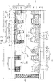
- FIG. 3 is a cross-sectional view taken along line II-II' of FIG. 1 .
- FIG. 4 is a plan view illustrating an embodiment of a partition wall and an upper dam included in the display device 10 of FIG. 3 .
- the display device 10 may include the lower panel 100, the upper panel 200, the filling member 300 and the sealing member 400.
- the lower panel 100 may include a lower substrate 110, a gate insulating layer 120, an interlayer insulating layer 130, a planarization layer 140, a pixel defining layer 150, a driving element TR, a light emitting element 160, an encapsulation layer 170, and a lower dam 180.
- the driving element TR may include an active layer AL, a gate electrode GE, a source electrode SE and a drain electrode DE.
- the light emitting element 160 may include a pixel electrode 161, an emission layer 162 and a counter electrode 163.
- the lower substrate 110 may define or include (e.g., have) the display area DA and the peripheral area PA.
- the lower substrate 110 may be a transparent insulating substrate.
- the lower substrate 110 may include glass, quartz, plastic, or the like.
- the active layer AL may be disposed in the display area DA, on the lower substrate 110.
- the active layer AL may include or be formed of amorphous silicon, polycrystalline silicon, oxide semiconductor or the like.
- the active layer AL may include a source area and a drain area each doped with impurities, and a channel area which is disposed between the source area and the drain area.
- a buffer layer may be disposed between the lower substrate 110 and the active layer AL.
- the buffer layer may prevent or reduce penetration of foreign substances from the lower substrate 110 into a component or layer above the buffer layer.
- the buffer layer may include an inorganic insulating material such as silicon oxide, silicon nitride, silicon oxynitride, and/or the like.
- the gate insulating layer 120 may be disposed on the lower substrate 110.
- the gate insulating layer 120 may be disposed in an entirety of the display area DA and an entirety of the peripheral area PA, on the lower substrate 110.
- a portion of the gate insulating layer 120 disposed in the display area DA may cover the active layer AL, on the lower substrate 110.
- the gate insulating layer 120 may include an inorganic insulating material such as silicon oxide, silicon nitride, silicon oxynitride and/or the like.
- the gate electrode GE may be disposed in the display area DA, on the gate insulating layer 120.
- the gate electrode GE may overlap the channel area of the active layer AL.
- the gate electrode GE may include a metal, an alloy, a conductive metal oxide, a conductive metal nitride, a transparent conductive material and/or the like.
- the gate electrode GE may include molybdenum (Mo), copper (Cu) and/or the like.
- the interlayer insulating layer 130 may be disposed on the gate insulating layer 120.
- the interlayer insulating layer 130 may be disposed in an entirety of the display area DA and an entirety of the peripheral area PA, on the gate insulating layer 120.
- a portion of the interlayer insulating layer 130 disposed in the display area DA may cover the gate electrode GE on the gate insulating layer 120.
- the interlayer insulating layer 130 may include an inorganic insulating material such as silicon oxide, silicon nitride, silicon oxynitride and/or the like.
- the source electrode SE and the drain electrode DE may be disposed in the display area DA, on the interlayer insulating layer 130.
- the source electrode SE and the drain electrode DE may be electrically connected to the source area and the drain area of the active layer AL, respectively.
- Each of the source electrode SE and the drain electrode DE may include a metal, an alloy, a conductive metal oxide, a conductive metal nitride, a transparent conductive material and/or the like.
- each of the source electrode SE and the drain electrode DE may include at least one of aluminium (Al), titanium (Ti), copper (Cu) and/or the like.
- the active layer AL, the gate electrode GE, the source electrode SE and the drain electrode DE may together form the driving element TR.
- the planarization layer 140 may be disposed in the display area DA, on the interlayer insulating layer 130.
- the planarization layer 140 may cover the source electrode SE and the drain electrode DE, on the interlayer insulating layer 130.
- the planarization layer 140 may have a substantially flat upper surface (e.g., without a stepped portion corresponding to the source electrode SE and the drain electrode DE).
- the planarization layer 140 may include an organic insulating material such as polyimide ("PI") or the like.
- the planarization layer 140 may have a multi-layered structure including a lower layer including an inorganic insulating material and an upper layer including an organic insulating material.
- the pixel electrode 161 may be disposed in the display area DA, on the planarization layer 140.
- the pixel electrode 161 may be electrically connected to the source electrode SE or the drain electrode DE. That is, the pixel electrode 161 may be disposed on the driving element TR, and may be electrically connected to the driving element TR.
- the pixel electrode 161 may include a metal, an alloy, a conductive metal oxide, a conductive metal nitride, a transparent conductive material and/or the like. In an embodiment, for example, the pixel electrode 161 may include silver (Ag), indium tin oxide ("ITO”) and/or the like.
- the pixel defining layer 150 may be disposed in the display area DA, on the planarization layer 140.
- the pixel defining layer 150 may partially cover the pixel electrode 161 on the planarization layer 140.
- the pixel defining layer 150 may define a pixel opening which exposes a portion of the pixel electrode 161 to outside the pixel defining layer 150.
- the pixel opening may expose a central portion of the pixel electrode 161, and the pixel defining layer 150 may cover a peripheral portion (e.g., edge) of the pixel electrode 161.
- the pixel defining layer 150 may include an organic insulating material such as polyimide ("PI”) or the like.
- the emission layer 162 may be disposed on the pixel electrode 161 which is exposed by the pixel opening of the pixel defining layer 150. That is, the emission layer 162 may be disposed in the pixel opening.
- the emission layer 162 may be disposed between the pixel electrode 161 and the counter electrode 163. That is, the pixel electrode 161 and the counter electrode 163 may face each other with the emission layer 162 therebetween.
- the emission layer 162 may include at least one of an organic light emitting material and a quantum dot.
- the organic light emitting material may include a low molecular weight organic compound or a high molecular weight organic compound.
- the low molecular weight organic compound may include at least one of copper phthalocyanine, N,N'-diphenylbenzidine, tris-(8-hydroxyquinoline)aluminium and/or the like
- the high molecular weight organic compound may include at least one of poly(3,4-ethylenedioxythiophene), polyaniline, poly(p-phenylene vinylene), polyfluorene and/or the like.
- the counter electrode 163 may be disposed on the emission layer 162 and may correspond to the pixel electrode 161. In an embodiment, the counter electrode 163 may also be disposed on the pixel defining layer 150. That is, the counter electrode 163 may extend from the emission layer 162 in the pixel opening, along a sidewall of the pixel defining layer 150 which defines the pixel opening and along an upper surface of the pixel defining layer 150, without being limited thereto.
- the counter electrode 163 may include a metal, an alloy, a conductive metal oxide, a conductive metal nitride, a transparent conductive material and/or the like.
- the counter electrode 163 may include aluminium (Al), platinum (Pt), silver (Ag), magnesium (Mg), gold (Au), chromium (Cr), tungsten (W), titanium (Ti) and/or the like.
- the pixel electrode 161, the emission layer 162 and the counter electrode 163 may together form the light emitting element 160.
- the encapsulation layer 170 may be disposed on the counter electrode 163.
- the encapsulation layer 170 may cover the light emitting element 160.
- the encapsulation layer 170 may encapsulate the display area DA to protect the light emitting element 160 from external impurities.
- the encapsulation layer 170 may include at least one inorganic encapsulation layer and at least one organic encapsulation layer.
- the encapsulation layer 170 may include a first inorganic encapsulation layer 171, a second inorganic encapsulation layer 173 which faces the first inorganic encapsulation layer 171, and an organic encapsulation layer 172 disposed between the first inorganic encapsulation layer 171 and the second inorganic encapsulation layer 173.
- the first inorganic encapsulation layer 171 may be disposed on the counter electrode 163.
- the first inorganic encapsulation layer 171 may have a substantially uniform thickness along the profile of the counter electrode 163.
- the first inorganic encapsulation layer thickness may be taken in a direction normal to the profile of the counter electrode 163.
- the organic encapsulation layer 172 may be disposed on the first inorganic encapsulation layer 171.
- the organic encapsulation layer 172 may have a substantially flat upper surface without a step corresponding to a profile of the first inorganic encapsulation layer 171.
- the second inorganic encapsulation layer 173 may be disposed on the organic encapsulation layer 172.
- the second inorganic encapsulation layer 173 may have a substantially uniform thickness and may have a substantially flat upper surface.
- the lower dam 180 may be disposed in the peripheral area PA, on the lower substrate 110. In an embodiment, for example, the lower dam 180 may be disposed in the peripheral area PA, on the interlayer insulating layer 130.
- the lower dam 180 may include a plurality of dams (e.g., dam patterns) including a first lower dam 181 and a second lower dam 182.
- the first lower dam 181 may include a first sub-dam 181a and a second sub-dam 181b.
- the first lower dam 181 may be closer to the display area DA than the second lower dam 182.
- the first sub-dam 181a may be extended around (e.g., surround) the display area DA in a plan view.
- the second sub-dam 181b may be spaced apart from the first sub-dam 181a in a direction along the lower substrate 110 and may be extended around (e.g., surround) the first sub-dam 181a in a plan view.
- the second sub-dam 181b may be further from the display area DA than the first sub-dam 181a.
- the first sub-dam 181a may include a first layer 1811a (e.g., first pattern) and a second layer 1812a (e.g., second pattern) which is disposed on the first layer 1811a.
- the first layer 1811a of the first sub-dam 181a may include substantially the same material as the planarization layer 140, and may be substantially simultaneously (or concurrently) provided or formed with the planarization layer 140. That is, the first layer 1811a of the first sub-dam 181a is in a same layer as the planarization layer 140.
- the second layer 1812a of the first sub-dam 181a may include substantially the same material as the pixel defining layer 150, and may be substantially simultaneously (or concurrently) provided or formed with the pixel defining layer 150. That is, the second layer 1812a of the first sub-dam 181a is in a same layer as the pixel defining layer 150. As being in a same layer, elements may be respective portions or patterns of a same material layer on the lower substrate 110.
- the second sub-dam 181b may include a first layer 1811b and a second layer 1812b which is disposed on the first layer 1811b.
- the first layer 1811b of the second sub-dam 181b may include substantially the same material as the planarization layer 140, and may be substantially simultaneously (or concurrently) provided or formed with the planarization layer 140.
- the second layer 1812b of the second sub-dam 181b may include substantially the same material as the pixel defining layer 150, and may be substantially simultaneously (or concurrently) provided or formed with the pixel defining layer 150.
- the first and second sub-dams 181a and 181b may further include third layers which are respectively disposed on the second layers 1812a and 1812b.
- the third layers may include substantially the same material as a spacer (not illustrated) which is disposed on the pixel defining layer 150, and may be substantially simultaneously (or concurrently) provided or formed with the spacer.
- the first lower dam 181 may prevent or reduce overflowing of an organic material of the organic encapsulation layer 172 from the display area DA to outside of the first lower dam 181 which is in the peripheral area PA. (e.g., to the left side of the first lower dam 181 of FIG. 3 ). That is, an edge of the organic encapsulation layer 172 may be disposed on the first lower dam 181 (e.g., corresponding to or an inside of the first lower dam 181).
- the second lower dam 182 may be spaced apart from the first lower dam 181 and may extend along or around (e.g., surround) the first lower dam 181.
- the second lower dam 182 may be spaced apart from the second sub-dam 181b and may extend along or around (e.g., surround) the second sub-dam 181b.
- the second lower dam 182 may include a first layer 1821 and a second layer 1822 which is disposed on the first layer 1821.
- the first layer 1821 of the second lower dam 182 may include substantially the same material as the planarization layer 140, and may be substantially simultaneously (or concurrently) provided or formed with the planarization layer 140.
- the second layer 1822 of the second lower dam 182 may include substantially the same material as the pixel defining layer 150 and may be substantially simultaneously (or concurrently) provided or formed with the pixel defining layer 150.
- portions of the lower dam 180 and the upper dam 280 may have a length extending along a respective outer edge of the display device 10 (e.g., length direction) and a width which is taken in a direction crossing the length direction such as a direction perpendicular thereto.
- the second lower dam 182 may support a mask structure used for a mask process during a manufacturing process of the display device 10.
- the second lower dam 182 may function as a buffer when supporting the mask structure.
- the second lower dam 182 may prevent or reduce a transmission of cracks into the display area DA.
- FIG. 3 illustrates that the first and second inorganic encapsulation layers 171 and 173 extend from the display area to cover the first lower dam 181 in the peripheral area PA and do not cover the second lower dam 182 (e.g., spaced apart from the second lower dam 182), but embodiments are not limited thereto.
- the first and second inorganic encapsulation layers 171 and 173 may extend from the display area DA and entirely cover both of the first lower dam 181 and the second lower dam 182 in the peripheral area PA.
- the upper panel 200 may include an upper substrate 210, a first color filter layer 222 (e.g., first color filter pattern), a second color filter layer 224 (e.g., second color filter pattern), a third color filter layer 226 (e.g., third color filter pattern) (e.g., first to third color filter layers 222, 224 and 226), a light blocking layer 223 (e.g., light blocking pattern), a low refractive layer 230, a first passivation layer 240, a partition wall 260, a first color conversion part 252 and a second color conversion part 254 (e.g., first and second color conversion parts 252 and 254), a transmission part 256, a second passivation layer 270 and an upper dam 280.
- the first color filter layer 222, the second color filter layer 224, and the third color filter layer 226 may together form a color filter layer.
- the first color conversion part 252, the second color conversion part 254 and the transmission part 256 may together provide a
- the upper substrate 210 may be disposed on the lower panel 100 and may face the lower substrate 110.
- the upper substrate 210 may include glass, quartz, plastic or the like.
- the upper substrate 210 may include a light emitting area and a light blocking area BA in the display area DA.
- each of the pixel areas PXA may include the light emitting area and the light blocking area BA.
- An incident light which is generated by the lower panel 100 and incident into the upper panel 200 may be emitted to outside the display device 10 through the light emitting area.
- the light emitting area may include a plurality of light emitting areas including a first light emitting area LA1, a second light emitting area LA2 and a third light emitting area LA3 (e.g., first to third light emitting areas LA1, LA2 and LA3).
- Transmitted lights having different colors may be emitted from the first to third light emitting areas LA1, LA2, and LA3, respectively.
- the first light emitting area LA1 may emit a first transmitted light having a first color
- the second light emitting area LA2 may emit a second transmitted light having a second color
- the third light emitting area LA3 may emit a third transmitted light having a third color.
- the first color may be blue
- the second color may be red
- the third color may be green.
- the incident light may have the first color.
- embodiments are not limited thereto.
- the first to third light emitting areas LA1, LA2, and LA3 may be spaced apart from each other in a plan view, and may be arranged in a repeated sequence.
- the light blocking area BA may extend along or around (e.g., surround) the first to third light emitting areas LA1, LA2, and LA3 in a plan view.
- the first to third color filter layers 222, 224, and 226 may be disposed in the display area DA under the upper substrate 210 and may overlap the light emitting area.
- the first color filter layer 222 may overlap or correspond to the first light emitting area LA1 and may selectively transmit a light having the first color.
- the second color filter layer 224 may overlap or correspond to the second light emitting area LA2 and may selectively transmit a light having the second color.
- the third color filter layer 226 may overlap or correspond to the third light emitting area LA3 and may selectively transmit a light having the third color.
- the light blocking layer 223 may be disposed in the display area DA under the upper substrate 210 and may overlap or correspond to the light blocking area BA. In an embodiment, for example, an entirety of the light blocking layer 223 may be disposed in the light blocking area BA so that the light blocking layer 223 may extend along or around (e.g., surround) each of the first to third light emitting areas LA1, LA2 and LA3 in a plan view. The light blocking layer 223 may prevent or reduce color mixing of lights emitted from the first to third light emitting areas LA1, LA2 and LA3 adjacent to each other. In an embodiment, for example, the light blocking layer 223 may include a light blocking material such as black pigment, dye, carbon black and/or the like.
- the low refractive layer 230 may be disposed in the display area DA under the upper substrate 210.
- a refractive index of the low refractive layer 230 may be smaller than each of a refractive index of the first color conversion part 252, a refractive index of the second color conversion part 254 and a refractive index of the transmission part 256. Accordingly, the low refractive layer 230 may improve light extraction efficiency so that luminance and lifespan of the display device 10 may be improved.
- FIG. 3 illustrates that the low refractive layer 230 is disposed between the color filter layer (e.g., the first to third color filter layers 222, 224, and 226) and the partition wall 260, or between the color filter layer and the color conversion layer (e.g., the first color conversion part 252, the second color conversion part 254 and the transmission part 256), but embodiments are not limited thereto.
- the low refractive layer 230 may be disposed under the partition wall 260 or under the color conversion layer (e.g., the first color conversion part 252, the second color conversion part 254 and the transmission part 256).
- a first low refractive layer may be disposed between the color filter layer (e.g., the first to third color filter layers 222, 224, and 226) and the partition wall 260, or between the color filter layer and the color conversion layer (e.g., the first color conversion part 252, the second color conversion part 254 and the transmission part 256), and a second low refractive layer may be disposed under the partition wall 260 or under the color conversion layer (e.g., the first color conversion part 252, the second color conversion part 254 and the transmission part 256).
- the low refractive layer 230 may be omitted.
- an element When referred to as being under, an element may be further from the upper substrate 210 than another element along the thickness direction.
- the first passivation layer 240 may be disposed under the upper substrate 210. In an embodiment, for example, the first passivation layer 240 may be disposed in an entirety of the display area DA and an entirety of the peripheral area PA, under the upper substrate 210. The first passivation layer 240 may extend from the display area DA to cover the first color filter layer 222, the second color filter layer 224, the third color filter layer 226, the light blocking layer 223 and the low refractive layer 230 which are under the upper substrate 210. In an embodiment, for example, the first passivation layer 240 may be disposed only in the display area DA, under the upper substrate 210. The first passivation layer 240 may include an inorganic insulating material such as silicon oxide, silicon nitride, silicon oxynitride and/or the like.
- the partition wall 260 may be disposed in the display area DA, under the upper substrate 210.
- a plurality of openings may be provided or formed in the partition wall 260.
- the plurality of openings defined in or by portions of the partition wall 260 may expose elements of the first to third light emitting areas LA1, LA2 and LA3, respectively, to outside the partition wall 260.
- the partition wall 260 may form a space (e.g., opening) which receives an ink composition for providing or forming the first color conversion part 252, the second color conversion part 254 and the transmission part 256.
- the partition wall 260 may overlap or correspond to an entirety of the light blocking area BA, and may have a grid shape or a matrix shape in a plan view.
- the partition wall 260 may include an organic material such as a photoresist, an epoxy resin, a phenolic resin, an acrylic resin, a silicone resin and/or the like.
- the partition wall 260 may further include a light blocking material.
- at least a portion of the partition wall 260 may include the light blocking material such as a pigment, a dye, a carbon black and/or the like.
- the first and second color conversion parts 252 and 254 may be disposed in the display area DA, under the upper substrate 210, and may overlap the light emitting area.
- the first color conversion part 252 may overlap the second light emitting area LA2 and the second color conversion part 254 may overlap the third light emitting area LA3.
- the first color conversion part 252 may overlap the second light emitting area LA2.
- the first color conversion part 252 may convert (e.g., wavelength convert) the incident light into the second transmitted light having the second color.
- the first color conversion part 252 may include a resin part 252a and a wavelength-converting particle 252b provided in plural including wavelength-converting particles 252b.
- each of the wavelength-converting particles 252b may include a quantum dot.
- the quantum dot may be defined as a nano-crystalline semiconductor material.
- the quantum dot may absorb an incident light and emit a light having a wavelength different from a wavelength of the incident light.
- the quantum dot may have a diameter (e.g., an average particle size) equal to or less than about 100 nanometers (nm).
- the quantum dot may have a diameter of about 1 nanometer (nm) to about 20 nm.
- each of the wavelength-converting particles 252b may include a quantum dot that absorbs blue light and emits red light.
- the wavelength-converting particles 252b may be disposed in the resin part 252a.
- the resin part 252a may include an epoxy resin, an acrylic resin, a phenolic resin, a melamine resin, a cardo resin, an imide resin and/or the like.
- the first color conversion part 252 may further include a scattering particle 252c provided in plural including scattering particles 252c.
- the scattering particles 252c may scatter the incident light without substantially changing the wavelength of the incident light. Therefore, a path of a light progressing in (e.g., progressing through) the first color conversion part 252 may be increased.
- the scattering particles 252c may include a metal oxide or an organic material.
- the first color conversion part 252 may change the wavelength of the incident light having a blue color (e.g., blue incident light) to emit the second transmitted light having a red color (e.g., red transmitted light). A remainder of the blue incident light, which is not color-changed in the first color conversion part 252, may be blocked by the second color filter layer 224. Accordingly, the second light emitting area LA2 may selectively emit the red transmitted light.
- a blue color e.g., blue incident light
- red color e.g., red transmitted light
- the second color conversion part 254 may overlap the third light emitting area LA3.
- the second color conversion part 254 may convert the incident light into the third transmitted light having the third color.
- the second color conversion part 254 may include a resin part 254a and a wavelength-converting particle 254b provided in plural including wavelength-converting particles 254b.
- the resin part 254a may include substantially the same material as the resin part 252a of the first color conversion part 252.
- a scattering particle 254c may be provided in plural including scattering particles 254c and may include substantially the same material as the scattering particles 252c of the first color conversion part 252.
- each of the wavelength-converting particles 254b may include a quantum dot that absorbs blue light and emits green light.
- the second color conversion part 254 may change the wavelength of the incident light having a blue color (e.g., blue incident light) to emit the third transmitted light having a green color (e.g., green transmitted light). A remainder of the blue incident light, which is not color-changed in the second color conversion part 254, may be blocked by the third color filter layer 226. Accordingly, the third light emitting area LA3 may selectively emit the green transmitted light.
- each of the quantum dots included in the first and second color conversion parts 252 and 254 may include a II-VI group compound, a III-V group compound, a IV-VI group compound, a IV group element, a IV group compound, or a combination thereof.
- the II-VI group compound may include a binary compound selected from CdSe, CdTe, ZnS, ZnSe, ZnTe, ZnO, HgS, HgSe, HgTe, MgSe, MgS and a combination thereof, a ternary compound selected from CdSeS, CdSeTe, CdSTe, ZnSeS, ZnSeTe, ZnSTe, HgSeS, HgSeTe, HgSTe, CdZnS, CdZnSe, CdZnTe, CdHgS, CdHgSe, CdHgTe, HgZnS, HgZnSe, HgZnTe, MgZnSe, MgZnS and a combination thereof, or a quaternary compound selected from HgZnTeS, CdZnSeS, CdZnSeTe, CdZ
- the III-V group compound may include a binary compound selected from GaN, GaP, GaAs, GaSb, AlN, AlP, AlAs, AlSb, InN, InP, InAs, InSb and a combination thereof, a ternary compound selected from GaNP, GaNAs, GaNSb, GaPAs, GaPSb, AlNP,AlNAs, AINSb, AlPAs, AlPSb, InNP, InNAs, InNSb, InPAs, InPSb and a combination thereof, or a quaternary compound selected from GaAlNP, GaAlNAs, GaAlNSb, GaAlPAs, GaAlPSb, GaInNP, GaInNAs, GaInNSb, GaInPAs, GaInPSb, InAlNP, InAlNAs, InAlNSb, InAlPAs, InAlPSb and a combination thereof.
- the IV-VI group compound may include a binary compound selected from SnS, SnSe, SnTe, PbS, PbSe, PbTe and a combination thereof, a ternary compound selected from SnSeS, SnSeTe, SnSTe, PbSeS, PbSeTe, PbSTe, SnPbS, SnPbSe, SnPbTe and a combination thereof, or a quaternary compound selected from SnPbSSe, SnPbSeTe, SnPbSTe and a combination thereof.
- the IV group element may include Si, Ge or a combination thereof.
- the IV group compound may include a binary compound selected from SiC, SiGe and a combination thereof.
- the quantum dot may have a core-shell structure including a core and a shell which surrounds the core.
- the core and the shell may include different materials.
- quantum dots included in the first and second color conversion parts 252 and 254 include the same material, light emitted from the respective first and second color conversion parts 252 and 254 may have different wavelengths from each other according to sizes of the quantum dots of the first and second color conversion parts 252 and 254.
- the smaller a size of a quantum dot the shorter a wavelength of light emitted from the quantum dot. Accordingly, light of different visible colors may be emitted by adjusting sizes of the quantum dots within the first and second color conversion parts 252 and 254.
- the transmission part 256 may be disposed in the display area DA, under the upper substrate 210, and may overlap the first light emitting area LA1.
- the transmission part 256 may include a resin part 256a and a scattering particle 256c provided in plural including scattering particles 256c.
- the resin part 256a may include substantially the same material as the resin part 252a of the first color conversion part 252.
- the scattering particles 256c may include substantially the same material as the scattering particles 252c of the first color conversion part 252.
- the transmission part 256 may not convert the incident light, and may emit the first transmitted light substantially the same as (e.g., substantially the same wavelength as) the incident light (e.g., unconverted). In an embodiment, for example, the transmission part 256 may absorb the incident light having a blue color (e.g., blue incident light) and emit the third transmitted light having a blue color.
- the transmission part 256 may absorb the incident light having a blue color (e.g., blue incident light) and emit the third transmitted light having a blue color.
- the first color conversion part 252, the second color conversion part 254 and the transmission part 256 may be disposed in each of the plurality of openings defined in the partition wall 260, respectively.
- the partition wall 260 may surround side surfaces of the first color conversion part 252, the second color conversion part 254 and the transmission part 256.
- the second passivation layer 270 may be disposed under the upper substrate 210.
- the second passivation layer 270 may be disposed in an entirety of the display area DA and an entirety of the peripheral area PA, under the upper substrate 210.
- the second passivation layer 270 may cover the partition wall 260, the first color conversion part 252, the second color conversion part 254, the transmission part 256 and the upper dam 280 which are under the upper substrate 210.
- the second passivation layer 270 may be disposed only in the display area DA, under the upper substrate 210.
- the second passivation layer 270 may be included in the lower panel 100, such as disposed on the encapsulation layer 170 and further from the lower substrate 110 than the encapsulation layer 170.
- the second passivation layer 270 may include an inorganic insulating material such as silicon oxide, silicon nitride, silicon oxynitride and/or the like.
- the upper dam 280 may be disposed in the peripheral area PA, under the upper substrate 210.
- the upper dam 280 may be disposed in the peripheral area PA, under the first passivation layer 240 which extends from the display area DA to define an extended portion of the first passivation layer 240 in the peripheral area PA.
- the upper dam 280 may be spaced apart from the partition wall 260 which is disposed in the display area DA.
- the upper dam 280 may include a first upper dam 281 and a second upper dam 282.
- the first upper dam 281 may be closer to the display area DA than the second upper dam 282.
- the upper substrate 210 may have an outer edge which is furthest from the display area DA, and the second upper dam 282 may be closest to the outer edge among the first upper dam 281 and the second upper dam 282.
- the first upper dam 281 may extend along or around (e.g., surround) the display area DA.
- the first upper dam 281 may be spaced apart from the partition wall 260 in the direction along the upper substrate 210, and may extend along or around the partition wall 260.
- the first upper dam 281 may have a hollow rectangular shape (e.g., a rectangular frame shape) in a plan view.
- a first opening OP1 may be defined or formed between the partition wall 260 and the first upper dam 281. That is, the first opening OP1 may be defined as a space at which the first upper dam 281 is spaced apart from the partition wall 260.
- the first opening OP1 may have a hollow rectangular shape (e.g., a rectangular frame shape) in a plan view.
- the first opening OP1 is open in a direction away from the upper substrate 210.
- the first opening OP1 may be open to the gap defined between the lower panel 100 and the upper panel 200 along the thickness direction.
- the first opening OP1 may accommodate a portion of the filling member 300 positioned in the peripheral area PA. This will be described in detail later.
- the second upper dam 282 may be spaced apart from the first upper dam 281, and may be extended along or around the first upper dam 281 in the plan view.
- the second upper dam 282 may have a hollow rectangular shape (e.g., a rectangular frame shape which has an open volume) in a plan view.
- a second opening OP2 may be defined or formed between the first upper dam 281 and the second upper dam 282. That is, the second opening OP2 may be defined as a space at which the second upper dam 282 is spaced apart from the first upper dam 281.
- the second opening OP2 may have a hollow rectangular shape (e.g., a rectangular frame shape which has an open volume) in a plan view.
- the second opening OP2 is open in a direction away from the upper substrate 210. Similar to the first opening OP1, the second opening OP2 may be open to the gap defined between the lower panel 100 and the upper panel 200 along the thickness direction.
- the second opening OP2 may accommodate a portion of the filling member 300 positioned in the peripheral area PA (refer to dotted line in FIG. 3 ).
- each of the first and second upper dams 281 and 282 may include substantially the same material as the partition wall 260, and may be substantially simultaneously (or concurrently) provided or formed with the partition wall 260.
- each of the first and second upper dams 281 and 282 may have substantially the same or similar thickness as the partition wall 260.
- the thickness may be a maximum dimension of an element along the thickness direction (e.g., third direction), for example, the vertical direction in FIG. 3 .
- the first upper dam 281 may overlap the first lower dam 181, and the second upper dam 282 may overlap the second lower dam 182.
- the first upper dam 281 may be positioned corresponding to the first lower dam 181 and spaced apart from the first lower dam 181 along the thickness direction.
- the second inorganic encapsulation layer 173 covering the first lower dam 181 on the lower substrate 110 may be spaced apart from the second passivation layer 270 covering the first upper dam 281 under the upper substrate 210.
- the second upper dam 282 may be positioned corresponding to the second lower dam 182 and spaced apart from the second lower dam 182 along the thickness direction.
- the first and second upper dams 281 and 282 which respectively correspond to the first and second lower dams 181 and 182 may contribute to maintaining a gap in the peripheral area PA between the lower panel 100 and the upper panel 200. Accordingly, a reliability of the display device 10 may be improved.
- the filling member 300 may be disposed in the display area DA between the lower substrate 110 and the upper substrate 210, at the gap therebetween.
- the filling member 300 may be disposed between the second inorganic encapsulation layer 173 included in the lower panel 100 and the second passivation layer 270 included in the upper panel 200.
- the filling member 300 may include a material which transmits light.
- the filling member 300 may include an organic material such as a silicone resin, an epoxy resin, an epoxy-acrylic resin and/or the like.
- the filling member 300 may include an appropriate and/or suitable material for matching a refractive index.
- the filling member 300 may function as a buffer against external pressure applied to the display device 10.
- the filling member 300 may maintain the gap between the lower panel 100 and the upper panel 200 (e.g., gap-maintaining layer).
- the filling member 300 disposed in the display area DA may extend from the display area DA and into the peripheral area PA so that a portion of the filling member 300 may be positioned in the first opening OP1 (e.g., an extended portion of the filling member 300). That is, the filling member 300 may be partially positioned in the first opening OP1. In an embodiment, for example, a portion of the filling member 300 may be positioned in the second opening OP2 (refer to a dotted line in FIG. 3 ).
- the upper panel 200 and the lower panel 100 may be combined with each other by the sealing member 400.
- the filling member 300 may be compressed by the combination of the upper panel 200 and the lower panel 100 so that the filling member 300 in the display area DA may extend and flow into the peripheral area PA.
- the amount of the filling member 300 extending to the peripheral area PA may be different.
- the openings may not be provided or formed between the partition wall 260 and the upper dam 280.
- a width e.g., a width in left and right directions of FIG. 3
- the width of the portion of the filling member 300 positioned in the peripheral area PA cannot be easily controlled so that the reliability of the conventional display device may be reduced.
- a gap may be defined or formed between the sealing member 400 and the upper panel 200 within the conventional display device. Accordingly, foreign substances may penetrate into the gap so that defects of the conventional display device may occur.
- the first upper dam 281 may be spaced apart from the partition wall 260, and the first opening OP1 may be defined or formed between the partition wall 260 and the first upper dam 281.
- the first opening OP1 may accommodate a portion of the filling member 300 positioned in the peripheral area PA. Accordingly, the first upper dam 281 may prevent or reduce overflowing of the filling member 300 to outside of the first upper dam 281 (e.g., to the left side of the first upper dam 281 of FIG. 3 ).
- the second upper dam 282 may be spaced apart from the first upper dam 281, and the second opening OP2 may be defined or formed between the first upper dam 281 and the second upper dam 282.
- the second opening OP2 may accommodate a portion of the filling member 300 flowing beyond the first upper dam 281. Accordingly, even if the amount of the filling member 300 extending to the peripheral area PA is relatively large so that the filling member 300 overflows to the outside of the first upper dam 281, the second upper dam 282 may prevent or reduce overflowing of the filling member 300 to an outside of the second upper dam 282 (e.g., to the left side of the second upper dam 282 of FIG. 3 ).
- a width e.g., a width in left and right directions
- the reliability of the display device 10 may be improved.
- the sealing member 400 may be disposed in the peripheral area PA between the lower substrate 110 and the upper substrate 210, and the lower substrate 110 and the upper substrate 210 may be combined with each other by the sealing member 400.
- the sealing member 400 may be positioned outside of the first and second upper dams 281 and 282 (e.g., at the left side of the first and second upper dams 281 and 282 of FIG. 3 ).
- the sealing member 400 may be spaced apart from the partition wall 260 with the first and second upper dams 281 and 282 therebetween in a direction along the upper substrate 210.
- the sealing member 400 may be spaced apart from the first and second upper dams 281 and 282 to extend along and/or surround the first and second upper dams 281 and 282.
- the sealing member 400 may have a rectangular shape (e.g., a rectangular frame shape) in a plan view.
- the sealing member 400 may have various planar shapes corresponding to a planar shape of the lower panel 100 and/or the upper panel 200.
- the sealing member 400 may have a corresponding planar shape of a hollow triangle, a hollow rhombus, a hollow polygon, a hollow circle, a hollow oval or the like in a plan view.
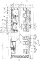
- FIG. 5 is a cross-sectional view illustrating an embodiment of the display device 10 taken along the line II-II' of FIG. 1 .
- portions of the first upper dam 281 may have a length extending along a respective outer edge of the display device 10 (e.g., length direction) and a width which is taken in a direction crossing the length direction such as a direction perpendicular thereto.
- the first upper dam 281 may overlap or correspond to both of the first lower dam 181 and the second lower dam 182.
- the second upper dam 282 may be omitted, and the first upper dam 281 may be provided or formed as a single body which overlaps both of the first and second lower dams 181 and 182. That is, the first upper dam 281 may be provided or formed to have a width (e.g., width in left and right directions) corresponding to a width occupied by the first and second lower dams 181 and 182.
- the width of the first upper dam 281 of the embodiment of FIG. 5 may be greater than the width of the first upper dam 281 of the embodiment of FIG. 3 .
- a portion of the filling member 300 positioned in the peripheral area PA may extend into the first opening OP1.
- a portion of the filling member 300 may be positioned under a lower surface of the first upper dam 281 which is furthest from the upper substrate 210 (refer to a dotted line in FIG. 5 ). That is, a portion of the filling member 300 may face the upper substrate 210 with the first upper dam 281 therebetween.
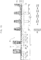
- FIG. 6 is a cross-sectional view illustrating an embodiment of the display device 10 taken along the line II-II' of FIG. 1 .
- FIG. 7 is a cross-sectional view illustrating an embodiment of the display device 10 taken along the line II-II' of FIG. 1 .
- the display device 10 may further include an organic layer 290 disposed between the upper substrate 210 and the upper dam 280.
- the organic layer 290 may overlap each of the first upper dam 281, the second upper dam 282, the first opening OP1 and the second opening OP2. That is, the organic layer 290 may be disposed in an entirety of the peripheral area PA between the upper substrate 210 and the upper dam 280.
- a portion of the first passivation layer 240 which is disposed in the peripheral area PA may cover the organic layer 290 under the upper substrate 210. That is, the first passivation layer 240 may be disposed between the organic layer 290 and the upper dam 280.
- the organic layer 290 may include substantially the same material as at least one of the first color filter layer 222, the second color filter layer 224, the third color filter layer 226, the light blocking layer 223, and the low refractive layer 230.
- the organic layer 290 may have a single-layered structure or a multi-layered structure along the thickness direction. In an embodiment, for example, the organic layer 290 may have a multi-layered structure including a plurality of layers including different materials.
- the organic layer 290 may be defined by an extended portion of as at least one of the first color filter layer 222, the second color filter layer 224, the third color filter layer 226, the light blocking layer 223, and the low refractive layer 230.
- the organic layer 290 may include first to fifth organic layers 291, 292, 293, 294 and 295 sequentially stacked in order from the upper substrate 210.
- the first organic layer 291 may include substantially the same material as the light blocking layer 223, and may be substantially simultaneously (or concurrently) provided or formed with the light blocking layer 223. That is, the light blocking layer 223 in the display area DA may extend from the display area DA to the peripheral area PA to define an extended portion of the light blocking layer 223. The extended portion of the light blocking layer 223 may define the first organic layer 291.
- the second organic layer 292 may include substantially the same material as the first color filter layer 222, and may be substantially simultaneously (or concurrently) provided or formed with the first color filter layer 222.
- the third organic layer 293 may include substantially the same material as the second color filter layer 224, and may be substantially simultaneously (or concurrently) provided or formed with the second color filter layer 224.
- the fourth organic layer 294 may include substantially the same material as the third color filter layer 226, and may be substantially simultaneously (or concurrently) provided or formed with the third color filter layer 226.
- the fifth organic layer 295 may include substantially the same material as the low refractive layer 230, and may be substantially simultaneously (or concurrently) provided or formed with the low refractive layer 230.
- the organic layer 290 may include second to fifth organic layers 292, 293, 294 and 295 sequentially stacked in order from the upper substrate 210.
- the light blocking layer 223 may be omitted, and the first to third color filter layers 222, 224 and 226 may be disposed to overlap the light blocking area BA of the display area DA.
- the first to third color filter layers 222, 224 and 226 disposed to overlap the light blocking area BA may prevent or reduce color mixing of the first to third light emitting areas LA1, LA2 and LA3 adjacent to each other.
- the second organic layer 292 may include substantially the same material as the first color filter layer 222, and may be substantially simultaneously (or concurrently) provided or formed with the first color filter layer 222.
- the third organic layer 293 may include substantially the same material as the second color filter layer 224, and may be substantially simultaneously (or concurrently) provided or formed with the second color filter layer 224.
- the fourth organic layer 294 may include substantially the same material as the third color filter layer 226, and may be substantially simultaneously (or concurrently) provided or formed with the third color filter layer 226.
- the fifth organic layer 295 may include substantially the same material as the low refractive layer 230, and may be substantially simultaneously (or concurrently) provided or formed with the low refractive layer 230.
- embodiments are not limited to the multi-layered structure of the organic layer 290 described with reference to FIGS. 6 and 7 .
- the multi-layered structure of the organic layer 290 may be variously modified corresponding to a stacking structure in the display area DA of the upper panel 200 and/or a method of manufacturing the upper panel 200.
- at least one of the first to fifth organic layers 291, 292, 293, 294 and 295 may be omitted, or another layer may be added.
- an organic layer 290 may not be disposed between the upper substrate 210 and the upper dam 280, an organic layer 290 having a single-layered structure may be disposed between the upper substrate 210 and the upper dam 280, or an organic layer 290 having a multi-layered structure including two or more layers may be disposed between the upper substrate 210 and the upper dam 280.
- the organic layer 290 having the single-layered structure or the multi-layered structure may be disposed in the peripheral area PA between the upper substrate 210 and the upper dam 280.
- the organic layer 290 may overlap both of the first and second upper dams 281 and 282. Accordingly, a separation distance along the thickness direction between the first upper dam 281 and the first lower dam 181 and a separation distance along the thickness direction between the second upper dam 282 and the second lower dam 282 may be relatively small. Accordingly, the organic layer 290 may contribute to maintaining the gap in the peripheral area PA between the lower panel 100 and the upper panel 200.
- the organic layer 290 disposed in an entirety of the peripheral area PA may reduce reflection of external light incident from outside the display device 10 and into the display device 10 through the upper substrate 210.
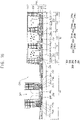
- FIG. 8 is a cross-sectional view illustrating an embodiment of the display device 10 taken along the line II-II' of FIG. 1 .
- FIG. 9 is a cross-sectional view illustrating an embodiment of a display device 10 taken along the line II-II' of FIG. 1 .
- the organic layer 290 may not overlap the first and second openings OP1 and OP2 (e.g., may be spaced apart from the openings).
- the organic layer 290 has a multi-layered structure including a plurality of layers, at least one of the plurality of layers may not overlap the first and second openings OP1 and OP2.
- all of the plurality of layers of the organic layer 290 may not overlap the first and second openings OP1 and OP2.
- each of the first to fifth organic layers 291, 292, 293, 294 and 295 may not overlap the first and second openings OP1 and OP2.
- the first organic layer 291 may include a first-first organic layer 291a (e.g., first organic pattern) and a first-second organic layer 291b (e.g., second organic pattern) which is spaced apart from the first-first organic layer 291a.
- the first-first organic layer 291a may overlap or correspond to the first upper dam 281 and may not overlap the first opening OP1.
- the first-first organic layer 291a may not overlap the second upper dam 282 and the second opening OP2. That is, the first-first organic layer 291a may be spaced apart from each of the first opening OP1, the second opening OP2 and the second upper dam 282 in a plan view.
- the first-first organic layer 291a may have a width (e.g., a width in left and right directions of FIG. 8 ) corresponding to a width of the first upper dam 281.
- the first-second organic layer 291b may overlap or correspond to the second upper dam 282 and may not overlap the second opening OP2. In addition, the first-second organic layer 291b may not overlap the first upper dam 281 and the first opening OP1. That is, the first-second organic layer 291b may be spaced apart from each of the first opening OP1, the second opening OP2 and the first upper dam 281 in a plan view. In other words, the first-second organic layer 291b may have a width (e.g., a width in left and right directions) corresponding to a width of the second upper dam 282.
- the second organic layer 292 may include a second-first organic layer 292a and a second-second organic layer 292b (e.g., first and second organic patterns).
- the third organic layer 293 may include a third-first organic layer 293a and a third-second organic layer 293b.
- the fourth organic layer 294 may include a fourth-first organic layer 294a and a fourth-second organic layer 294b.
- the fifth organic layer 295 may include a fifth-first organic layer 295a and a fifth-second organic layer 295b.
- Each of the second-first organic layer 292a, the third-first organic layer 293a, the fourth-first organic layer 294a and the fifth-first organic layer 295a may have substantially the same or similar planar shape as the first-first organic layer 291a. That is, each of the second-first organic layer 292a, the third-first organic layer 293a, the fourth-first organic layer 294a and the fifth-first organic layer 295a may overlap or correspond to the first upper dam 281, and may not overlap each of the second upper dam 282, the first opening OP1 and the second opening OP2.
- Each of the second-second organic layer 292b, the third-second organic layer 293b, the fourth-second organic layer 294b and the fifth-second organic layer 295b may have substantially the same or similar planar shape as the first-second organic layer 291b. That is, each of the second-second organic layer 292b, the third-second organic layer 293b, the fourth-second organic layer 294b and the fifth-second organic layer 295b may overlap or correspond to the second upper dam 282, and may not overlap each of the first upper dam 281, the first opening OP1 and the second opening OP2.
- each of the plurality of layers included in the organic layer 290 having a multi-layered structure may be disposed to overlap the first and second upper dams 281 and 282. Accordingly, the separation distance along the thickness direction between the first upper dam 281 and the first lower dam 181 and the separation distance along the thickness direction between the second upper dam 282 and the second lower dam 182 may be relatively less. Accordingly, the organic layer 290 may contribute to maintaining the gap in the peripheral area PA between the lower panel 100 and the upper panel 200.
- each of the plurality of layers may not overlap the first and second openings OP1 and OP2. Accordingly, the size of each of the first and second openings OP1 and OP2 to accommodate the portion of the filling member 300 positioned in the peripheral area PA may be relatively large. Accordingly, a width (e.g., a width in left and right directions) of the portion of the filling member 300 positioned in the peripheral area PA may be easily controlled.
- At least one of the plurality of layers of the organic layer 290 may overlap or correspond to the first and second openings OP1 and OP2, and at least one of the plurality of layers of the organic layer 290 may not overlap the first and second openings OP1 and OP2.
- the first organic layer 291 may overlap both of the first and second openings OP1 and OP2, and each of the second to fifth organic layers 292, 293, 294 and 295 may not overlap the first and second openings OP1 and OP2. That is, the second organic layer 292 may include the second-first organic layer 292a and the second-second organic layer 292b.
- the third organic layer 293 may include the third-first organic layer 293a and the third-second organic layer 293b.
- the fourth organic layer 294 may include the fourth-first organic layer 294a and the fourth-second organic layer 294b.
- the fifth organic layer 295 may include the fifth-first organic layer 295a and the fifth-second organic layer 295b.
- At least one of the plurality of layers included in the organic layer 290 having a multi-layered structure may be disposed in an entirety of the peripheral area PA.
- at least one of the plurality of layers may be disposed so as not to overlap the first and second openings OP1 and OP2.
- a portion of the plurality of layers may be disposed in an entirety of the peripheral area PA so as to overlap the first and second openings OP1 and OP2, and remaining layers may be disposed in the peripheral area PA so as to overlap only the first and second upper dams 281 and 282 (e.g., not overlap the first and second openings OP1 and OP2) in plurality as necessary (e.g., to prevent or reduce reflection of external light).
- FIGS. 10 to 18 are cross-sectional views illustrating an embodiment of a method of manufacturing or providing a display device 10.
- FIGS. 10 to 18 may illustrate a method of providing or manufacturing the display device 10 related to FIG. 9 .
- the light blocking layer 223 and the first organic layer 291 may be provided or formed on the upper substrate 210.
- the light blocking layer 223 may be provided or formed in the display area DA on the upper substrate 210.
- the light blocking layer 223 may be provided or formed as a plurality of patterns which overlap or correspond to the light blocking area BA in the display area DA.
- the light blocking layer 223 may include or be formed of an organic material including a black pigment.
- the first organic layer 291 may be provided or formed in the peripheral area PA on the upper substrate 210. In an embodiment, for example, the first organic layer 291 may be formed in an entirety of the peripheral area PA. In an embodiment, for example, the first organic layer 291 may include or be formed of an organic material including a black pigment.
- the light blocking layer 223 and the first organic layer 291 may be substantially simultaneously (or concurrently) provided or formed.
- a pre-organic layer may include or be formed of an organic material including a black pigment on the upper substrate 210.
- the pre-organic layer may be patterned by a photolithography or the like to substantially simultaneously form the light blocking layer 223 and the first organic layer 291 as respective organic patterns of a same material layer (e.g., in a same layer).
- the first color filter layer 222, the second-first organic layer 292a and the second-second organic layer 292b may be provided or formed on the upper substrate 210.
- the first color filter layer 222 may be provided or formed in the display area DA on the upper substrate 210.
- the first color filter layer 222 may be provided or formed to overlap or correspond to the first light emitting area LA1 in the display area DA.
- the first color filter layer 222 may include or be formed of an organic material including a pigment having the first color.
- the first color may be blue.
- the second-first organic layer 292a and the second-second organic layer 292b may be provided or formed on the first organic layer 291.
- the second-first organic layer 292a may be provided or formed to be spaced apart from the display area DA and to surround the display area DA.
- the second-second organic layer 292b may be provided or formed to be spaced apart from the second-first organic layer 292a and to surround the second-first organic layer 292a.
- the second-first organic layer 292a and the second-second organic layer 292b may include or be formed of an organic material including a pigment having the first color.
- the first color filter layer 222, the second-first organic layer 292a and the second-second organic layer 292b may be substantially simultaneously (or concurrently) provided or formed.
- a pre-organic layer may include or be formed of an organic material including a pigment having the first color on the upper substrate 210 and the first organic layer 291.
- the pre-organic layer may be patterned by a photolithography or the like to substantially simultaneously form the first color filter layer 222, the second-first organic layer 292a and the second-second organic layer 292b as respective organic patterns of a same material layer (e.g., in a same layer).
- the second color filter layer 224, the third-first organic layer 293a and the third-second organic layer 293b may be provided or formed on the upper substrate 210.
- the second color filter layer 224 may be provided or formed in the display area DA on the upper substrate 210.
- the second color filter layer 224 may be provided or formed to overlap the second light emitting area LA2 in the display area DA.
- the second color filter layer 224 may include or be formed of an organic material including a pigment having the second color.
- the second color may be red.
- the third-first organic layer 293a may be provided or formed on the second-first organic layer 292a.
- the third-first organic layer 293a may be provided or formed to have substantially the same width (e.g., width in left and right directions) as the second-first organic layer 292a.
- the third-second organic layer 293b may be provided or formed on the second-second organic layer 292b.
- the third-second organic layer 293b may be provided or formed to have substantially the same width (e.g., width in left and right directions) as the second-second organic layer 292b.
- the third-first organic layer 293a and the third-second organic layer 293b may be formed of an organic material including a pigment having the second color.
- the second color filter layer 224, the third-first organic layer 293a and the third-second organic layer 293b may be substantially simultaneously (or concurrently) provided or formed.
- a pre-organic layer may be provided or formed of an organic material including a pigment having the second color on the upper substrate 210, the first organic layer 291, the second-first organic layer 292a and the second-second organic layer 292b.
- the pre-organic layer may be patterned by a photolithography or the like to substantially simultaneously form the second color filter layer 224, the third-first organic layer 293a and the third-second organic layer 293b as respective organic patterns of a same material layer (e.g., in a same layer).
- the third color filter layer 226, the fourth-first organic layer 294a and the fourth-second organic layer 294b may be provided or formed on the upper substrate 210.
- the third color filter layer 226 may be provided or formed in the display area DA on the upper substrate 210.
- the third color filter layer 226 may be provided or formed to overlap the third light emitting area LA3 in the display area DA.
- the third color filter layer 226 may include or be formed of an organic material including a pigment having the third color.
- the second color may be green.
- the fourth-first organic layer 294a may be provided or formed on the third-first organic layer 293a.
- the fourth-first organic layer 294a may be provided or formed to have substantially the same width (e.g., width in left and right directions) as the third-first organic layer 293a.
- the fourth-second organic layer 294b may be provided or formed on the third-second organic layer 293b.
- the fourth-second organic layer 294b may be provided or formed to have substantially the same width (e.g., width in left and right directions) as the third-second organic layer 293b.
- the fourth-first organic layer 294a and the fourth-second organic layer 294b may include or be formed of an organic material including a pigment having the third color.
- the third color filter layer 226, the fourth-first organic layer 294a and the fourth-second organic layer 294b may be substantially simultaneously (or concurrently) provided or formed.
- a pre-organic layer may include or be formed of an organic material including a pigment having the third color on the upper substrate 210, the first organic layer 291, the third-first organic layer 293a and the third-second organic layer 293b.
- the pre-organic layer may be patterned by a photolithography or the like to substantially simultaneously form the third color filter layer 226, the fourth-first organic layer 294a and the fourth-second organic layer 294b as respective organic patterns of a same material layer (e.g., in a same layer).
- the low refractive layer 230, the fifth-first organic layer 295a and the fifth-second organic layer 295b may be provided or formed on the upper substrate 210.
- the low refractive layer 230 may be provided or formed in the display area DA on the upper substrate 210.
- the low refractive layer 230 may be provided or formed in the display area DA on the first to third color filter layers 222, 224 and 226 and the light blocking layer 223.
- the low refractive layer 230 may include or be formed of an organic material having a relatively low refractive index such as acryl, polyimide, polyamide and/or the like.
- the fifth-first organic layer 295a may be provided or formed on the fourth-first organic layer 294a.
- the fifth-first organic layer 295a may be provided or formed to have substantially the same width (e.g., width in left and right directions) as the fourth-first organic layer 294a.
- the fifth-second organic layer 295b may be provided or formed on the fourth-second organic layer 294b.
- the fifth-second organic layer 295b may be provided or formed to have substantially the same width (e.g., width in left and right directions) as the fourth-second organic layer 294b.
- the fifth-first organic layer 295a and the fifth-second organic layer 295b may include or be formed of an organic material such as acryl, polyimide, polyamide, and/or the like.
- the low refractive layer 230, the fifth-first organic layer 295a and the fifth-second organic layer 295b may be substantially simultaneously (or concurrently) provided or formed.
- a pre-organic layer may be provided or formed of an organic material such as acryl, polyimide, polyamide and/or the like on the first to third color filter layers 222, 224 and 226, the light blocking layer 223, the first organic layer 291, the fourth-first organic layer 294a and the fourth-second organic layer 294b.
- the pre-organic layer may be patterned by a photolithography or the like to substantially simultaneously form the low refractive layer 230, the fifth-first organic layer 295a and the fifth-second organic layer 295b as respective organic patterns of a same material layer (e.g., in a same layer).
- the first passivation layer 240 may be provided or formed on the upper substrate 210. In an embodiment, for example, the first passivation layer 240 may be formed in an entirety of the display area DA and an entirety of the peripheral area PA on the upper substrate 210. In an embodiment, for example, the first passivation layer 240 may cover the low refractive layer 230 and the organic layer 290.
- the first passivation layer 240 may include or be formed of an inorganic insulating material such as silicon oxide, silicon nitride, silicon oxynitride, and/or the like.
- the partition wall 260, the first upper dam 281 and the second upper dam 282 may be provided or formed on the first passivation layer 240.
- the partition wall 260 may be provided or formed in the display area DA on the first passivation layer 240.
- the partition wall 260 may be provided or formed to overlap the light blocking area BA in the display area DA. Accordingly, a plurality of openings may be defined or formed by portions of the partition wall 260. The plurality of openings may expose corresponding ones of the first to third light emitting areas LA1, LA2 and LA3, respectively.
- the partition wall 260 may include an organic material and a light blocking material.
- the first upper dam 281 may be provided or formed to overlap the second-first organic layer 292a, the third-first organic layer 293a, the fourth-first organic layer 294a and the fifth-first organic layer 295a on the first passivation layer 240.
- the first upper dam 281 may be provided or formed to be spaced apart from the partition wall 260 and/or to surround the partition wall 260. Accordingly, the first opening OP1 may be defined or formed between the first upper dam 281 and the partition wall 260.
- the first upper dam 281 may include an organic material and/or a light blocking material.
- the second upper dam 282 may be provided or formed to overlap the second-second organic layer 292b, the third-second organic layer 293b, the fourth-second organic layer 294b and the fifth-second organic layer 295b on the first passivation layer 240.
- the second upper dam 282 may be provided or formed to be spaced apart from the first upper dam 281 and/or to surround the first upper dam 281. Accordingly, the second opening OP2 may be defined or formed between the first upper dam 281 and the second upper dam 282.
- the second upper dam 282 may include an organic material and/or a light blocking material.
- the partition wall 260, the first upper dam 281 and the second upper dam 282 may be substantially simultaneously (or concurrently) provided or formed.
- a pre-organic layer may be provided or formed of an organic material and a light blocking material on the first passivation layer 240.
- the pre-organic layer may be patterned by a photolithography or the like to substantially simultaneously form the partition wall 260, the first upper dam 281 and the second upper dam 282 as respective patterns of a same material layer (e.g., in a same layer).
- the transmission part 256, the first color conversion part 252 and the second color conversion part 254 may be provided or formed in the display area DA on the upper substrate 210.
- the transmission part 256, the first color conversion part 252 and the second color conversion part 254 may be provided or formed to overlap the first to third light emitting area LA1, LA2 and LA3, respectively.
- the transmission part 256, the first color conversion part 252 and the second color conversion part 254 may be provided or formed in corresponding ones of the plurality of openings defined or formed in the partition wall 260.
- the transmission part 256, the first color conversion part 252 and the second color conversion part 254 may be provided or formed by an inkjet process.
- an ink including a corresponding composition e.g., corresponding wavelength-converting particles
- An inkjet printing apparatus may be used to provide the ink.
- the inkjet printing apparatus may provide the ink inside the plurality of openings through a plurality of nozzles, respectively. Accordingly, the plurality of openings may be filled with the corresponding composition.
- the compositions in the plurality of openings may be cured to form the transmission part 256, the first color conversion part 252 and the second color conversion part 254. In an embodiment, for example, the compositions may be cured by heat and/or light.
- the second passivation layer 270 may be provided or formed on the upper substrate 210 so that the upper panel 200 may be provided or formed. In an embodiment, for example, the second passivation layer 270 may be provided or formed in an entirety of the display area DA and an entirety of the peripheral area PA, on the upper substrate 210. In an embodiment, for example, the second passivation layer 270 may cover the partition wall 260, the first color conversion part 252, the second color conversion part 254, the transmission part 256, the first upper dam 281 and the second upper dam 282. That is, the second passivation layer 270 may be common to each of the partition wall 260, the first color conversion part 252, the second color conversion part 254, the transmission part 256, the first upper dam 281 and the second upper dam 282.
- the second passivation layer 270 may include or be formed of an inorganic insulating material such as silicon oxide, silicon nitride, silicon oxynitride and/or the like.
- the filling member 300 and the sealing member 400 may be applied on the upper panel 200.
- the filling member 300 may be applied to the display area DA, on the second passivation layer 270.
- the sealing member 400 may be applied to the peripheral area PA, on the second passivation layer 270.
- the lower panel 100 including a plurality of pixels may be disposed facing the upper panel 200.
- the upper panel 200 and the lower panel 100 which face each other may be combined with each other by the sealing member 400.
- a material of the sealing member 400 may be cured by heat and/or light.
- the filling member 300 When the upper panel 200 and the lower panel 100 are combined with each other, the filling member 300 may be compressed so that a portion of the filling member 300 may extend from the display area DA and flow into the peripheral area PA.
- the portion of the filling member 300 (e.g., extended portion) may be accommodated in the first opening OP1. That is, the first upper dam 281 may prevent or reduce overflowing of the filling member 300 to outside of the first upper dam 281 (e.g., to the left side of the first upper dam 281 of FIG. 18 ).
- the portion of the filling member 300 may be accommodated in the first and second openings OP1 and OP2.
- the second upper dam 282 may prevent or reduce overflowing of the filling member 300 to outside of the second upper dam 282 (e.g., to the left side of the second upper dam 282 of FIG. 18 ). Accordingly, even if the amount of the filling member 300 applied to the upper panel 200 or the degree of compression of the filling member 300 varies, the width (e.g., the width in left and right directions) of the extended portion of the filling member 300 in the peripheral area PA may be easily controlled by the first and second upper dams 281 and 282. Accordingly, the reliability of the display device 10 may be improved.
Landscapes
- Physics & Mathematics (AREA)
- Optics & Photonics (AREA)
- Engineering & Computer Science (AREA)
- Microelectronics & Electronic Packaging (AREA)
- Electroluminescent Light Sources (AREA)
- Devices For Indicating Variable Information By Combining Individual Elements (AREA)
Abstract
Description
- Embodiments relate to a display device. More particularly, embodiments relate to a display device including an upper panel, a lower panel, and a filling member disposed between the upper panel and the lower panel.
- Flat panel display devices are replacing cathode ray tube display devices as display devices due to lightweight and thin characteristics. As representative examples of such flat panel display devices, there are liquid crystal display devices and organic light emitting diode display devices.
- The flat panel display device may include a lower panel and an upper panel which is combined with the lower panel. Pixels may be disposed in the lower panel, and color conversion parts may be disposed in the upper panel. The flat panel display device may have a display area in which an image is displayed and a peripheral area which surrounds the display area. A sealing member may be disposed in the peripheral area between the upper panel and the lower panel. A filling member to function as a buffer against external pressure may be disposed in the display area between the upper panel and the lower panel.
- Embodiments provide a display device with improved reliability.
- Additional features will be set forth in the description which follows, and in part will be apparent from the description, or may be learned by practice of the invention.
- An embodiment of a display device includes a lower panel including a display area and a peripheral area which is adjacent to the display area, an upper panel facing the lower panel, and a filling member which is in the display area between the lower panel and the upper panel. The upper panel includes a partition wall defining a plurality of openings in the display area, a first upper dam in the peripheral area and spaced apart from the partition wall, and a first opening defined between the partition wall and the first upper dam. The filling member extends from the display area and into the first opening defined between the partition wall and the first upper dam.
- In an embodiment, the partition wall may include an organic material. The first upper dam and the partition wall may be in a same layer of the upper panel.
- In an embodiment, the upper panel may further include an upper substrate facing each of the partition wall in the display area, and the first upper dam in the peripheral area, and an organic layer between the upper substrate and the first upper dam.
- In an embodiment, the organic layer may extend from between the upper substrate and the first upper dam, and may overlap the first opening defined between the partition wall and the first upper dam.
- In an embodiment, the organic layer may be spaced apart from the first opening defined between the partition wall and the first upper dam in a plan view.
- In an embodiment, the upper panel may further include color filter layers in the display area and between the upper substrate and the partition wall. The organic layer may be in a same layer of the upper panel as at least one of the color filter layers.
- In an embodiment, the upper panel may further include a light blocking layer between the upper substrate and the partition wall in the display area. The organic layer may be in a same layer of the upper panel as the light blocking layer.
- In an embodiment, the upper panel may further include color conversion parts in the plurality of openings of the partition wall, respectively, and having a refractive index, and a low refractive layer between the upper substrate and the color conversion parts and having a refractive index. The refractive index of the low refractive layer may be smaller than the refractive index of the color conversion parts. The organic layer may be in a same layer of the upper panel as the low refractive layer.
- In an embodiment, the organic layer which is between the upper substrate and the first upper dam of the upper panel may include a plurality of layers including different materials. At least one of the plurality of layers may overlap the first opening. At least one of the plurality of layers may be spaced apart from the first opening defined between the partition wall and the first upper dam in a plan view.
- In an embodiment, the lower panel may further include a first lower dam in the peripheral area and corresponding to the first upper dam of the upper panel, and a second lower dam in the peripheral area and spaced apart from the first lower dam. The first lower dam may be between the second lower dam and the display area.
- In an embodiment, the first upper dam of the upper panel may correspond to both the first lower dam and the second lower dam of the lower panel.
- In an embodiment, the upper panel may further include a second upper dam spaced apart from the first upper dam and corresponding to the second lower dam of the lower panel, and a second opening defined between the first upper dam and the second upper dam.
- In an embodiment, the filling member may extend from the display area and into the second opening defined between the first upper dam and the second upper dam.
- In an embodiment, the upper panel may further includes an upper substrate facing each of the partition wall in the display area and the second upper dam in the peripheral area, and an organic layer between the upper substrate and the second upper dam. The organic layer may extend from between the upper substrate and the second upper dam, and may overlap each of the first upper dam, the first opening and the second opening.
- In an embodiment, the upper panel may further include an upper substrate facing each of the partition wall in the display area and the second upper dam in the peripheral area, and an organic layer between the upper substrate and the second upper dam. The organic layer may be spaced apart from the second opening defined between the first upper dam and the second upper dam in a plan view.
- At least some of the above and other features of the invention are set out in the claims.
- One or more embodiments of the display device may include the lower panel, the upper panel combined with the lower panel, and the filling member in the display area between the lower panel and the upper panel. The upper panel may include the partition wall and the upper dam. The partition wall may be in the display area under the upper substrate. The upper dam may be in the peripheral area under the upper substrate and may be spaced apart from the partition wall. The opening may be between the partition wall and the upper dam. The opening may accommodate a portion of the filling member extending to the peripheral area. Accordingly, the upper dam may control a width of the portion of the filling member positioned in the peripheral area. Accordingly, the reliability of the display device may be improved.
- One or more embodiments of the display device may further include the lower dam overlapping the upper dam. The upper dam may overlap the lower dam so that the upper dam may contribute to maintaining a gap in the peripheral area between the lower panel and the upper panel. Accordingly, the reliability of the display device may be improved.
- It is to be understood that both the foregoing general description and the following detailed description are explanatory and are intended to provide further explanation of the invention as claimed.
- The accompanying drawings, which are included to provide a further understanding of the invention and are incorporated in and constitute a part of this specification, illustrate embodiments of the invention, and together with the description serve to explain the invention.
-
FIG. 1 is a plan view illustrating an embodiment of a display device. -
FIG. 2 is a cross-sectional view taken along line I-I' ofFIG. 2 . -
FIG. 3 is a cross-sectional view illustrating an embodiment of the display device taken along line II-II' ofFIG. 1 . -
FIG. 4 is a plan view illustrating an embodiment of a partition wall and an upper dam included in the display device ofFIG. 3 . -
FIG. 5 is a cross-sectional view illustrating an embodiment of a display device taken along line II-II' ofFIG. 1 . -
FIG. 6 is a cross-sectional view illustrating an embodiment of a display device taken along line II-II' ofFIG. 1 . -
FIG. 7 is a cross-sectional view illustrating an embodiment of a display device taken along line II-II' ofFIG. 1 . -
FIG. 8 is a cross-sectional view illustrating an embodiment of a display device taken along line II-II' ofFIG. 1 . -
FIG. 9 is a cross-sectional view illustrating an embodiment of a display device taken along line II-II' ofFIG. 1 . -
FIGS. 10 to 18 are cross-sectional views illustrating an embodiment of a method of providing a display device. - The invention will now be described more fully hereinafter with reference to the accompanying drawings, in which various embodiments are shown. This invention may, however, be embodied in many different forms, and should not be construed as limited to the embodiments set forth herein. Rather, these embodiments are provided so that this disclosure will be thorough and complete, and will fully convey the scope of the invention to those skilled in the art. Like reference numerals refer to like elements throughout.
- It will be understood that when an element is referred to as being related to another element such as being "on" another element, it can be directly on the other element or intervening elements may be present therebetween. In contrast, when an element is referred to as being related to another element such as being "directly on" another element, there are no intervening elements present.
- It will be understood that, although the terms "first," "second," "third" etc. may be used herein to describe various elements, components, regions, layers and/or sections, these elements, components, regions, layers and/or sections should not be limited by these terms. These terms are only used to distinguish one element, component, region, layer or section from another element, component, region, layer or section. Thus, "a first element," "component," "region," "layer" or "section" discussed below could be termed a second element, component, region, layer or section without departing from the teachings herein.
- The terminology used herein is for the purpose of describing particular embodiments only and is not intended to be limiting. As used herein, "a", "an," "the," and "at least one" do not denote a limitation of quantity, and are intended to include both the singular and plural, unless the context clearly indicates otherwise. For example, "an element" has the same meaning as "at least one element," unless the context clearly indicates otherwise. "At least one" is not to be construed as limiting "a" or "an." "Or" means "and/or." As used herein, the term "and/or" includes any and all combinations of one or more of the associated listed items. It will be further understood that the terms "comprises" and/or "comprising," or "includes" and/or "including" when used in this specification, specify the presence of stated features, regions, integers, steps, operations, elements, and/or components, but do not preclude the presence or addition of one or more other features, regions, integers, steps, operations, elements, components, and/or groups thereof.
- Furthermore, relative terms, such as "lower" or "bottom" and "upper" or "top," may be used herein to describe one element's relationship to another element as illustrated in the Figures. It will be understood that relative terms are intended to encompass different orientations of the device in addition to the orientation depicted in the Figures. For example, if the device in one of the figures is turned over, elements described as being on the "lower" side of other elements would then be oriented on "upper" sides of the other elements. The term "lower," can therefore, encompasses both an orientation of "lower" and "upper," depending on the particular orientation of the figure. Similarly, if the device in one of the figures is turned over, elements described as "below" or "beneath" other elements would then be oriented "above" the other elements. The terms "below" or "beneath" can, therefore, encompass both an orientation of above and below.
- "About" or "approximately" as used herein is inclusive of the stated value and means within an acceptable range of deviation for the particular value as determined by one of ordinary skill in the art, considering the measurement in question and the error associated with measurement of the particular quantity (i.e., the limitations of the measurement system). For example, "about" can mean within one or more standard deviations, or within ± 30%, 20%, 10% or 5% of the stated value.
- Unless otherwise defined, all terms (including technical and scientific terms) used herein have the same meaning as commonly understood by one of ordinary skill in the art to which this disclosure belongs. It will be further understood that terms, such as those defined in commonly used dictionaries, should be interpreted as having a meaning that is consistent with their meaning in the context of the relevant art and the present disclosure, and will not be interpreted in an idealized or overly formal sense unless expressly so defined herein.
- Embodiments are described herein with reference to cross section illustrations that are schematic illustrations of example embodiments. As such, variations from the shapes of the illustrations as a result, for example, of manufacturing techniques and/or tolerances, are to be expected. Thus, embodiments described herein should not be construed as limited to the particular shapes of regions as illustrated herein but are to include deviations in shapes that result, for example, from manufacturing. For example, a region illustrated or described as flat may, typically, have rough and/or nonlinear features. Moreover, sharp angles that are illustrated may be rounded. Thus, the regions illustrated in the figures are schematic in nature and their shapes are not intended to illustrate the precise shape of a region and are not intended to limit the scope of the present claims.
- Illustrative, non-limiting embodiments will be more clearly understood from the following detailed description in conjunction with the accompanying drawings.
-
FIG. 1 is a plan view illustrating an embodiment of adisplay device 10.FIG. 2 is a cross-sectional view taken along line I-I' ofFIG. 2 . - Referring to
FIGS. 1 and 2 , adisplay device 10 may include alower panel 100, anupper panel 200 and a sealingmember 400. Thelower panel 100 and theupper panel 200 may be combined with each other by the sealingmember 400. Theupper panel 200 faces thelower panel 100 along a thickness direction. - The
display device 10 may include (e.g., have) a display area DA and a peripheral area PA which is adjacent to the display area DA. An image may be displayed in the display area DA. The display area DA may include a pixel area PXA provided in plural including a plurality of pixel areas PXA. In an embodiment, the peripheral area PA may extend along or be around (e.g., surround) the display area DA in a plan view. Various components and layers of thedisplay device 10, for example, each of thelower panel 100 and theupper panel 200, may include (e.g., have) the display area DA and the peripheral area PA corresponding to those described above for thedisplay device 10. - The
display device 10 and various components and layers thereof may be disposed in a plane defined by a first direction and a second direction which crosses the first direction. Referring toFIG. 1 , the vertical and horizontal directions may variously represent the first direction and the second direction without being limited thereto. A thickness direction of thedisplay device 10 and various components and layers thereof may extend along a third direction crossing each of the first direction and the second direction. Referring toFIG. 2 , for example, the vertical direction may represent the third direction, while the horizontal direction may variously represent the first direction and the second direction without being limited thereto. A plan view may be a view along the third direction (e.g., along a thickness direction). - The
lower panel 100 may be a display panel including a plurality of pixels which are controlled or driven to generate an image. The pixels may be disposed in the display area DA in thelower panel 100. Each of the pixels may include alight emitting element 160 which generates and/or emits a light, and a driving element TR which is connected to thelight emitting element 160 to drive thelight emitting element 160. In an embodiment, for example, thelight emitting element 160 may include an organic light emitting diode. In an embodiment, thelight emitting element 160 may include a nano light emitting diode. The driving element TR may include a switching element such as a thin film transistor. - The
upper panel 200 may be a color conversion panel including color conversion parts. In an embodiment, for example, the color conversion parts may be disposed in the display area DA in theupper panel 200 and may convert a wavelength of the light generated by thelight emitting element 160 included in thelower panel 100. In an embodiment, for example, theupper panel 200 may further include color filter layers which transmit a light having a specific color (e.g., a light having a specific wavelength range). - The
lower panel 100 and theupper panel 200 may be combined with each other by the sealingmember 400. The sealingmember 400 may be disposed in the peripheral area PA which is between thelower panel 100 and theupper panel 200. In an embodiment, for example, the sealingmember 400 may not be disposed in the display area DA (e.g., may be excluded from the display area DA or spaced apart from the display area DA), but may be disposed in the peripheral area PA between thelower panel 100 and theupper panel 200 to surround the display area DA. - In a plan view, for example, the sealing
member 400 may have a hollow rectangular shape (e.g., a rectangular frame shape). However, embodiments are not limited thereto, and the sealingmember 400 may have various planar shapes corresponding to a planar shape of thelower panel 100 and/or theupper panel 200. In an embodiment, for example, when thelower panel 100 and/or theupper panel 200 has a planar shape such as a triangle, a rhombus, a polygon, a circle, an oval or the like, the sealingmember 400 may have a corresponding planar shape of a hollow triangle, a hollow rhombus, a hollow polygon, a hollow circle, a hollow oval or the like in a plan view. - In an embodiment, for example, the sealing
member 400 may include a frit or the like. In an embodiment, the sealingmember 400 may include a photocurable resin such as an epoxy acrylate resin, a polyester acrylate resin, a urethane acrylate resin, a polybutadiene acrylate resin, a silicone acrylate resin, an alkyl acrylate resin and/or the like. In an embodiment of providing thedisplay device 10, for example, a laser may be irradiated to a sealing member material of the sealingmember 400 which is disposed between thelower panel 100 and theupper panel 200. The sealing member material of the sealingmember 400 may be cured by the laser to combine thelower panel 100 and theupper panel 200 by the sealingmember 400. - A filling member 300 (of
FIG. 3 ) may be disposed in the display area DA between thelower panel 100 and theupper panel 200. In an embodiment, for example, the fillingmember 300 may function as a buffer against external pressure applied to the display device 10 (e.g., impact resistant layer). In an embodiment, for example, the fillingmember 300 may maintain a gap between thelower panel 100 and theupper panel 200 which is along the thickness direction. In an embodiment, for example, the fillingmember 300 which is in the display area DA may extend from the display area DA to the peripheral area PA so that a portion of the fillingmember 300 may be positioned in the peripheral area PA between thelower panel 100 and theupper panel 200. This will be described in detail later. The fillingmember 300 may fill an entirety of the gap defined between thelower panel 100 and theupper panel 200, without being limited thereto. - In an embodiment, the filling
member 300 may include a material which transmits light (e.g., light transmitting material). In an embodiment, for example, the filling member may include an organic material such as a silicone resin, an epoxy resin, an epoxy-acrylic resin and/or the like. In an embodiment, for example, the filling member may include an appropriate and/or suitable material for matching a refractive index of one or more components or layers within thedisplay device 10. -
FIG. 3 is a cross-sectional view taken along line II-II' ofFIG. 1 .FIG. 4 is a plan view illustrating an embodiment of a partition wall and an upper dam included in thedisplay device 10 ofFIG. 3 . - Referring to
FIGS. 3 and4 , thedisplay device 10 may include thelower panel 100, theupper panel 200, the fillingmember 300 and the sealingmember 400. Thelower panel 100 may include alower substrate 110, agate insulating layer 120, aninterlayer insulating layer 130, aplanarization layer 140, apixel defining layer 150, a driving element TR, alight emitting element 160, anencapsulation layer 170, and alower dam 180. The driving element TR may include an active layer AL, a gate electrode GE, a source electrode SE and a drain electrode DE. Thelight emitting element 160 may include apixel electrode 161, anemission layer 162 and acounter electrode 163. - The
lower substrate 110 may define or include (e.g., have) the display area DA and the peripheral area PA. Thelower substrate 110 may be a transparent insulating substrate. In an embodiment, for example, thelower substrate 110 may include glass, quartz, plastic, or the like. - The active layer AL may be disposed in the display area DA, on the
lower substrate 110. In an embodiment, for example, the active layer AL may include or be formed of amorphous silicon, polycrystalline silicon, oxide semiconductor or the like. The active layer AL may include a source area and a drain area each doped with impurities, and a channel area which is disposed between the source area and the drain area. - Although not illustrated in the drawing, a buffer layer may be disposed between the
lower substrate 110 and the active layer AL. The buffer layer may prevent or reduce penetration of foreign substances from thelower substrate 110 into a component or layer above the buffer layer. In an embodiment, for example, the buffer layer may include an inorganic insulating material such as silicon oxide, silicon nitride, silicon oxynitride, and/or the like. - The
gate insulating layer 120 may be disposed on thelower substrate 110. In an embodiment, for example, thegate insulating layer 120 may be disposed in an entirety of the display area DA and an entirety of the peripheral area PA, on thelower substrate 110. A portion of thegate insulating layer 120 disposed in the display area DA may cover the active layer AL, on thelower substrate 110. In an embodiment, for example, thegate insulating layer 120 may include an inorganic insulating material such as silicon oxide, silicon nitride, silicon oxynitride and/or the like. - The gate electrode GE may be disposed in the display area DA, on the
gate insulating layer 120. The gate electrode GE may overlap the channel area of the active layer AL. The gate electrode GE may include a metal, an alloy, a conductive metal oxide, a conductive metal nitride, a transparent conductive material and/or the like. In an embodiment, for example, the gate electrode GE may include molybdenum (Mo), copper (Cu) and/or the like. - The interlayer insulating
layer 130 may be disposed on thegate insulating layer 120. In an embodiment, for example, theinterlayer insulating layer 130 may be disposed in an entirety of the display area DA and an entirety of the peripheral area PA, on thegate insulating layer 120. A portion of the interlayer insulatinglayer 130 disposed in the display area DA may cover the gate electrode GE on thegate insulating layer 120. In an embodiment, for example, theinterlayer insulating layer 130 may include an inorganic insulating material such as silicon oxide, silicon nitride, silicon oxynitride and/or the like. - The source electrode SE and the drain electrode DE may be disposed in the display area DA, on the
interlayer insulating layer 130. The source electrode SE and the drain electrode DE may be electrically connected to the source area and the drain area of the active layer AL, respectively. Each of the source electrode SE and the drain electrode DE may include a metal, an alloy, a conductive metal oxide, a conductive metal nitride, a transparent conductive material and/or the like. In an embodiment, for example, each of the source electrode SE and the drain electrode DE may include at least one of aluminium (Al), titanium (Ti), copper (Cu) and/or the like. The active layer AL, the gate electrode GE, the source electrode SE and the drain electrode DE may together form the driving element TR. - The
planarization layer 140 may be disposed in the display area DA, on theinterlayer insulating layer 130. Theplanarization layer 140 may cover the source electrode SE and the drain electrode DE, on theinterlayer insulating layer 130. Theplanarization layer 140 may have a substantially flat upper surface (e.g., without a stepped portion corresponding to the source electrode SE and the drain electrode DE). In an embodiment, for example, theplanarization layer 140 may include an organic insulating material such as polyimide ("PI") or the like. In an embodiment, for example, theplanarization layer 140 may have a multi-layered structure including a lower layer including an inorganic insulating material and an upper layer including an organic insulating material. - The
pixel electrode 161 may be disposed in the display area DA, on theplanarization layer 140. Thepixel electrode 161 may be electrically connected to the source electrode SE or the drain electrode DE. That is, thepixel electrode 161 may be disposed on the driving element TR, and may be electrically connected to the driving element TR. Thepixel electrode 161 may include a metal, an alloy, a conductive metal oxide, a conductive metal nitride, a transparent conductive material and/or the like. In an embodiment, for example, thepixel electrode 161 may include silver (Ag), indium tin oxide ("ITO") and/or the like. - The
pixel defining layer 150 may be disposed in the display area DA, on theplanarization layer 140. Thepixel defining layer 150 may partially cover thepixel electrode 161 on theplanarization layer 140. Thepixel defining layer 150 may define a pixel opening which exposes a portion of thepixel electrode 161 to outside thepixel defining layer 150. In an embodiment, for example, the pixel opening may expose a central portion of thepixel electrode 161, and thepixel defining layer 150 may cover a peripheral portion (e.g., edge) of thepixel electrode 161. Thepixel defining layer 150 may include an organic insulating material such as polyimide ("PI") or the like. - The
emission layer 162 may be disposed on thepixel electrode 161 which is exposed by the pixel opening of thepixel defining layer 150. That is, theemission layer 162 may be disposed in the pixel opening. Theemission layer 162 may be disposed between thepixel electrode 161 and thecounter electrode 163. That is, thepixel electrode 161 and thecounter electrode 163 may face each other with theemission layer 162 therebetween. Theemission layer 162 may include at least one of an organic light emitting material and a quantum dot. - In an embodiment, the organic light emitting material may include a low molecular weight organic compound or a high molecular weight organic compound. The low molecular weight organic compound may include at least one of copper phthalocyanine, N,N'-diphenylbenzidine, tris-(8-hydroxyquinoline)aluminium and/or the like, and the high molecular weight organic compound may include at least one of poly(3,4-ethylenedioxythiophene), polyaniline, poly(p-phenylene vinylene), polyfluorene and/or the like.
- The
counter electrode 163 may be disposed on theemission layer 162 and may correspond to thepixel electrode 161. In an embodiment, thecounter electrode 163 may also be disposed on thepixel defining layer 150. That is, thecounter electrode 163 may extend from theemission layer 162 in the pixel opening, along a sidewall of thepixel defining layer 150 which defines the pixel opening and along an upper surface of thepixel defining layer 150, without being limited thereto. Thecounter electrode 163 may include a metal, an alloy, a conductive metal oxide, a conductive metal nitride, a transparent conductive material and/or the like. In an embodiment, for example, thecounter electrode 163 may include aluminium (Al), platinum (Pt), silver (Ag), magnesium (Mg), gold (Au), chromium (Cr), tungsten (W), titanium (Ti) and/or the like. Thepixel electrode 161, theemission layer 162 and thecounter electrode 163 may together form thelight emitting element 160. - The
encapsulation layer 170 may be disposed on thecounter electrode 163. Theencapsulation layer 170 may cover thelight emitting element 160. Theencapsulation layer 170 may encapsulate the display area DA to protect thelight emitting element 160 from external impurities. - The
encapsulation layer 170 may include at least one inorganic encapsulation layer and at least one organic encapsulation layer. In an embodiment, theencapsulation layer 170 may include a firstinorganic encapsulation layer 171, a secondinorganic encapsulation layer 173 which faces the firstinorganic encapsulation layer 171, and anorganic encapsulation layer 172 disposed between the firstinorganic encapsulation layer 171 and the secondinorganic encapsulation layer 173. - The first
inorganic encapsulation layer 171 may be disposed on thecounter electrode 163. In an embodiment, for example, the firstinorganic encapsulation layer 171 may have a substantially uniform thickness along the profile of thecounter electrode 163. The first inorganic encapsulation layer thickness may be taken in a direction normal to the profile of thecounter electrode 163. - The
organic encapsulation layer 172 may be disposed on the firstinorganic encapsulation layer 171. Theorganic encapsulation layer 172 may have a substantially flat upper surface without a step corresponding to a profile of the firstinorganic encapsulation layer 171. - The second
inorganic encapsulation layer 173 may be disposed on theorganic encapsulation layer 172. The secondinorganic encapsulation layer 173 may have a substantially uniform thickness and may have a substantially flat upper surface. - The
lower dam 180 may be disposed in the peripheral area PA, on thelower substrate 110. In an embodiment, for example, thelower dam 180 may be disposed in the peripheral area PA, on theinterlayer insulating layer 130. - In an embodiment, the
lower dam 180 may include a plurality of dams (e.g., dam patterns) including a firstlower dam 181 and a secondlower dam 182. In an embodiment, for example, the firstlower dam 181 may include a first sub-dam 181a and a second sub-dam 181b. The firstlower dam 181 may be closer to the display area DA than the secondlower dam 182. - The first sub-dam 181a may be extended around (e.g., surround) the display area DA in a plan view. The second sub-dam 181b may be spaced apart from the first sub-dam 181a in a direction along the
lower substrate 110 and may be extended around (e.g., surround) the first sub-dam 181a in a plan view. The second sub-dam 181b may be further from the display area DA than the first sub-dam 181a. - In an embodiment, the first sub-dam 181a may include a
first layer 1811a (e.g., first pattern) and asecond layer 1812a (e.g., second pattern) which is disposed on thefirst layer 1811a. In an embodiment, for example, thefirst layer 1811a of the first sub-dam 181a may include substantially the same material as theplanarization layer 140, and may be substantially simultaneously (or concurrently) provided or formed with theplanarization layer 140. That is, thefirst layer 1811a of the first sub-dam 181a is in a same layer as theplanarization layer 140. Thesecond layer 1812a of the first sub-dam 181a may include substantially the same material as thepixel defining layer 150, and may be substantially simultaneously (or concurrently) provided or formed with thepixel defining layer 150. That is, thesecond layer 1812a of the first sub-dam 181a is in a same layer as thepixel defining layer 150. As being in a same layer, elements may be respective portions or patterns of a same material layer on thelower substrate 110. - In an embodiment, the second sub-dam 181b may include a
first layer 1811b and asecond layer 1812b which is disposed on thefirst layer 1811b. In an embodiment, for example, thefirst layer 1811b of the second sub-dam 181b may include substantially the same material as theplanarization layer 140, and may be substantially simultaneously (or concurrently) provided or formed with theplanarization layer 140. Thesecond layer 1812b of the second sub-dam 181b may include substantially the same material as thepixel defining layer 150, and may be substantially simultaneously (or concurrently) provided or formed with thepixel defining layer 150. - In an embodiment, the first and second sub-dams 181a and 181b may further include third layers which are respectively disposed on the
second layers pixel defining layer 150, and may be substantially simultaneously (or concurrently) provided or formed with the spacer. - In a method of providing a
display device 10, for example, the firstlower dam 181 may prevent or reduce overflowing of an organic material of theorganic encapsulation layer 172 from the display area DA to outside of the firstlower dam 181 which is in the peripheral area PA. (e.g., to the left side of the firstlower dam 181 ofFIG. 3 ). That is, an edge of theorganic encapsulation layer 172 may be disposed on the first lower dam 181 (e.g., corresponding to or an inside of the first lower dam 181). - The second
lower dam 182 may be spaced apart from the firstlower dam 181 and may extend along or around (e.g., surround) the firstlower dam 181. In an embodiment, for example, the secondlower dam 182 may be spaced apart from the second sub-dam 181b and may extend along or around (e.g., surround) the second sub-dam 181b. - In an embodiment, the second
lower dam 182 may include afirst layer 1821 and asecond layer 1822 which is disposed on thefirst layer 1821. In an embodiment, for example, thefirst layer 1821 of the secondlower dam 182 may include substantially the same material as theplanarization layer 140, and may be substantially simultaneously (or concurrently) provided or formed with theplanarization layer 140. Thesecond layer 1822 of the secondlower dam 182 may include substantially the same material as thepixel defining layer 150 and may be substantially simultaneously (or concurrently) provided or formed with thepixel defining layer 150. - Taking
FIGS. 3 and4 together, portions of thelower dam 180 and theupper dam 280 may have a length extending along a respective outer edge of the display device 10 (e.g., length direction) and a width which is taken in a direction crossing the length direction such as a direction perpendicular thereto. - In a method of providing a
display device 10, for example, the secondlower dam 182 may support a mask structure used for a mask process during a manufacturing process of thedisplay device 10. In addition, the secondlower dam 182 may function as a buffer when supporting the mask structure. In addition, the secondlower dam 182 may prevent or reduce a transmission of cracks into the display area DA. -
FIG. 3 illustrates that the first and second inorganic encapsulation layers 171 and 173 extend from the display area to cover the firstlower dam 181 in the peripheral area PA and do not cover the second lower dam 182 (e.g., spaced apart from the second lower dam 182), but embodiments are not limited thereto. In embodiments, the first and second inorganic encapsulation layers 171 and 173 may extend from the display area DA and entirely cover both of the firstlower dam 181 and the secondlower dam 182 in the peripheral area PA. - The
upper panel 200 may include anupper substrate 210, a first color filter layer 222 (e.g., first color filter pattern), a second color filter layer 224 (e.g., second color filter pattern), a third color filter layer 226 (e.g., third color filter pattern) (e.g., first to third color filter layers 222, 224 and 226), a light blocking layer 223 (e.g., light blocking pattern), a lowrefractive layer 230, afirst passivation layer 240, apartition wall 260, a firstcolor conversion part 252 and a second color conversion part 254 (e.g., first and secondcolor conversion parts 252 and 254), atransmission part 256, asecond passivation layer 270 and anupper dam 280. The firstcolor filter layer 222, the secondcolor filter layer 224, and the thirdcolor filter layer 226 may together form a color filter layer. The firstcolor conversion part 252, the secondcolor conversion part 254 and thetransmission part 256 may together provide a color conversion layer. - The
upper substrate 210 may be disposed on thelower panel 100 and may face thelower substrate 110. In an embodiment, for example, theupper substrate 210 may include glass, quartz, plastic or the like. - In an embodiment, the
upper substrate 210 may include a light emitting area and a light blocking area BA in the display area DA. In an embodiment, for example, each of the pixel areas PXA may include the light emitting area and the light blocking area BA. An incident light which is generated by thelower panel 100 and incident into theupper panel 200 may be emitted to outside thedisplay device 10 through the light emitting area. In an embodiment, for example, the light emitting area may include a plurality of light emitting areas including a first light emitting area LA1, a second light emitting area LA2 and a third light emitting area LA3 (e.g., first to third light emitting areas LA1, LA2 and LA3). - Transmitted lights having different colors may be emitted from the first to third light emitting areas LA1, LA2, and LA3, respectively. In an embodiment, for example, the first light emitting area LA1 may emit a first transmitted light having a first color, the second light emitting area LA2 may emit a second transmitted light having a second color, and the third light emitting area LA3 may emit a third transmitted light having a third color. In an embodiment, for example, the first color may be blue, the second color may be red and the third color may be green. In an embodiment, for example, the incident light may have the first color. However, embodiments are not limited thereto.
- In an embodiment, as illustrated in
FIG. 4 , the first to third light emitting areas LA1, LA2, and LA3 may be spaced apart from each other in a plan view, and may be arranged in a repeated sequence. The light blocking area BA may extend along or around (e.g., surround) the first to third light emitting areas LA1, LA2, and LA3 in a plan view. - The first to third color filter layers 222, 224, and 226 may be disposed in the display area DA under the
upper substrate 210 and may overlap the light emitting area. In an embodiment, for example, the firstcolor filter layer 222 may overlap or correspond to the first light emitting area LA1 and may selectively transmit a light having the first color. The secondcolor filter layer 224 may overlap or correspond to the second light emitting area LA2 and may selectively transmit a light having the second color. The thirdcolor filter layer 226 may overlap or correspond to the third light emitting area LA3 and may selectively transmit a light having the third color. - The
light blocking layer 223 may be disposed in the display area DA under theupper substrate 210 and may overlap or correspond to the light blocking area BA. In an embodiment, for example, an entirety of thelight blocking layer 223 may be disposed in the light blocking area BA so that thelight blocking layer 223 may extend along or around (e.g., surround) each of the first to third light emitting areas LA1, LA2 and LA3 in a plan view. Thelight blocking layer 223 may prevent or reduce color mixing of lights emitted from the first to third light emitting areas LA1, LA2 and LA3 adjacent to each other. In an embodiment, for example, thelight blocking layer 223 may include a light blocking material such as black pigment, dye, carbon black and/or the like. - The low
refractive layer 230 may be disposed in the display area DA under theupper substrate 210. In an embodiment, for example, a refractive index of the lowrefractive layer 230 may be smaller than each of a refractive index of the firstcolor conversion part 252, a refractive index of the secondcolor conversion part 254 and a refractive index of thetransmission part 256. Accordingly, the lowrefractive layer 230 may improve light extraction efficiency so that luminance and lifespan of thedisplay device 10 may be improved. -
FIG. 3 illustrates that the lowrefractive layer 230 is disposed between the color filter layer (e.g., the first to third color filter layers 222, 224, and 226) and thepartition wall 260, or between the color filter layer and the color conversion layer (e.g., the firstcolor conversion part 252, the secondcolor conversion part 254 and the transmission part 256), but embodiments are not limited thereto. In an embodiment, for example, the lowrefractive layer 230 may be disposed under thepartition wall 260 or under the color conversion layer (e.g., the firstcolor conversion part 252, the secondcolor conversion part 254 and the transmission part 256). In an embodiment, for example, a first low refractive layer may be disposed between the color filter layer (e.g., the first to third color filter layers 222, 224, and 226) and thepartition wall 260, or between the color filter layer and the color conversion layer (e.g., the firstcolor conversion part 252, the secondcolor conversion part 254 and the transmission part 256), and a second low refractive layer may be disposed under thepartition wall 260 or under the color conversion layer (e.g., the firstcolor conversion part 252, the secondcolor conversion part 254 and the transmission part 256). In an embodiment, for example, the lowrefractive layer 230 may be omitted. When referred to as being under, an element may be further from theupper substrate 210 than another element along the thickness direction. - The
first passivation layer 240 may be disposed under theupper substrate 210. In an embodiment, for example, thefirst passivation layer 240 may be disposed in an entirety of the display area DA and an entirety of the peripheral area PA, under theupper substrate 210. Thefirst passivation layer 240 may extend from the display area DA to cover the firstcolor filter layer 222, the secondcolor filter layer 224, the thirdcolor filter layer 226, thelight blocking layer 223 and the lowrefractive layer 230 which are under theupper substrate 210. In an embodiment, for example, thefirst passivation layer 240 may be disposed only in the display area DA, under theupper substrate 210. Thefirst passivation layer 240 may include an inorganic insulating material such as silicon oxide, silicon nitride, silicon oxynitride and/or the like. - The
partition wall 260 may be disposed in the display area DA, under theupper substrate 210. A plurality of openings may be provided or formed in thepartition wall 260. In an embodiment, for example, as illustrated inFIG. 4 , the plurality of openings defined in or by portions of thepartition wall 260 may expose elements of the first to third light emitting areas LA1, LA2 and LA3, respectively, to outside thepartition wall 260. In an embodiment, for example, thepartition wall 260 may form a space (e.g., opening) which receives an ink composition for providing or forming the firstcolor conversion part 252, the secondcolor conversion part 254 and thetransmission part 256. In other words, thepartition wall 260 may overlap or correspond to an entirety of the light blocking area BA, and may have a grid shape or a matrix shape in a plan view. - In an embodiment, the
partition wall 260 may include an organic material such as a photoresist, an epoxy resin, a phenolic resin, an acrylic resin, a silicone resin and/or the like. Thepartition wall 260 may further include a light blocking material. In an embodiment, for example, at least a portion of thepartition wall 260 may include the light blocking material such as a pigment, a dye, a carbon black and/or the like. - The first and second
color conversion parts upper substrate 210, and may overlap the light emitting area. In an embodiment, for example, the firstcolor conversion part 252 may overlap the second light emitting area LA2 and the secondcolor conversion part 254 may overlap the third light emitting area LA3. - The first
color conversion part 252 may overlap the second light emitting area LA2. The firstcolor conversion part 252 may convert (e.g., wavelength convert) the incident light into the second transmitted light having the second color. In an embodiment, for example, the firstcolor conversion part 252 may include aresin part 252a and a wavelength-convertingparticle 252b provided in plural including wavelength-convertingparticles 252b. - In an embodiment, for example, each of the wavelength-converting
particles 252b may include a quantum dot. The quantum dot may be defined as a nano-crystalline semiconductor material. The quantum dot may absorb an incident light and emit a light having a wavelength different from a wavelength of the incident light. In an embodiment, the quantum dot may have a diameter (e.g., an average particle size) equal to or less than about 100 nanometers (nm). In an embodiment, the quantum dot may have a diameter of about 1 nanometer (nm) to about 20 nm. In an embodiment, each of the wavelength-convertingparticles 252b may include a quantum dot that absorbs blue light and emits red light. - The wavelength-converting
particles 252b may be disposed in theresin part 252a. In an embodiment, for example, theresin part 252a may include an epoxy resin, an acrylic resin, a phenolic resin, a melamine resin, a cardo resin, an imide resin and/or the like. - In an embodiment, the first
color conversion part 252 may further include ascattering particle 252c provided in plural including scatteringparticles 252c. The scatteringparticles 252c may scatter the incident light without substantially changing the wavelength of the incident light. Therefore, a path of a light progressing in (e.g., progressing through) the firstcolor conversion part 252 may be increased. In an embodiment, for example, the scatteringparticles 252c may include a metal oxide or an organic material. - In an embodiment, for example, the first
color conversion part 252 may change the wavelength of the incident light having a blue color (e.g., blue incident light) to emit the second transmitted light having a red color (e.g., red transmitted light). A remainder of the blue incident light, which is not color-changed in the firstcolor conversion part 252, may be blocked by the secondcolor filter layer 224. Accordingly, the second light emitting area LA2 may selectively emit the red transmitted light. - The second
color conversion part 254 may overlap the third light emitting area LA3. The secondcolor conversion part 254 may convert the incident light into the third transmitted light having the third color. In an embodiment, for example, the secondcolor conversion part 254 may include aresin part 254a and a wavelength-convertingparticle 254b provided in plural including wavelength-convertingparticles 254b. Theresin part 254a may include substantially the same material as theresin part 252a of the firstcolor conversion part 252. Ascattering particle 254c may be provided in plural including scatteringparticles 254c and may include substantially the same material as the scatteringparticles 252c of the firstcolor conversion part 252. - In an embodiment, each of the wavelength-converting
particles 254b may include a quantum dot that absorbs blue light and emits green light. In an embodiment, for example, the secondcolor conversion part 254 may change the wavelength of the incident light having a blue color (e.g., blue incident light) to emit the third transmitted light having a green color (e.g., green transmitted light). A remainder of the blue incident light, which is not color-changed in the secondcolor conversion part 254, may be blocked by the thirdcolor filter layer 226. Accordingly, the third light emitting area LA3 may selectively emit the green transmitted light. - In an embodiment, each of the quantum dots included in the first and second
color conversion parts - In an embodiment, for example, the II-VI group compound may include a binary compound selected from CdSe, CdTe, ZnS, ZnSe, ZnTe, ZnO, HgS, HgSe, HgTe, MgSe, MgS and a combination thereof, a ternary compound selected from CdSeS, CdSeTe, CdSTe, ZnSeS, ZnSeTe, ZnSTe, HgSeS, HgSeTe, HgSTe, CdZnS, CdZnSe, CdZnTe, CdHgS, CdHgSe, CdHgTe, HgZnS, HgZnSe, HgZnTe, MgZnSe, MgZnS and a combination thereof, or a quaternary compound selected from HgZnTeS, CdZnSeS, CdZnSeTe, CdZnSTe, CdHgSeS, CdHgSeTe, CdHgSTe, HgZnSeS, HgZnSeTe, HgZnSTe and a combination thereof.
- In an embodiment, for example, the III-V group compound may include a binary compound selected from GaN, GaP, GaAs, GaSb, AlN, AlP, AlAs, AlSb, InN, InP, InAs, InSb and a combination thereof, a ternary compound selected from GaNP, GaNAs, GaNSb, GaPAs, GaPSb, AlNP,AlNAs, AINSb, AlPAs, AlPSb, InNP, InNAs, InNSb, InPAs, InPSb and a combination thereof, or a quaternary compound selected from GaAlNP, GaAlNAs, GaAlNSb, GaAlPAs, GaAlPSb, GaInNP, GaInNAs, GaInNSb, GaInPAs, GaInPSb, InAlNP, InAlNAs, InAlNSb, InAlPAs, InAlPSb and a combination thereof.
- In an embodiment, for example, the IV-VI group compound may include a binary compound selected from SnS, SnSe, SnTe, PbS, PbSe, PbTe and a combination thereof, a ternary compound selected from SnSeS, SnSeTe, SnSTe, PbSeS, PbSeTe, PbSTe, SnPbS, SnPbSe, SnPbTe and a combination thereof, or a quaternary compound selected from SnPbSSe, SnPbSeTe, SnPbSTe and a combination thereof.
- In an embodiment, for example, the IV group element may include Si, Ge or a combination thereof. The IV group compound may include a binary compound selected from SiC, SiGe and a combination thereof.
- In an embodiment, for example, the quantum dot may have a core-shell structure including a core and a shell which surrounds the core. In an embodiment, for example, the core and the shell may include different materials.
- Even if the quantum dots included in the first and second
color conversion parts color conversion parts color conversion parts color conversion parts - The
transmission part 256 may be disposed in the display area DA, under theupper substrate 210, and may overlap the first light emitting area LA1. In an embodiment, for example, thetransmission part 256 may include aresin part 256a and ascattering particle 256c provided in plural including scatteringparticles 256c. Theresin part 256a may include substantially the same material as theresin part 252a of the firstcolor conversion part 252. The scatteringparticles 256c may include substantially the same material as the scatteringparticles 252c of the firstcolor conversion part 252. - The
transmission part 256 may not convert the incident light, and may emit the first transmitted light substantially the same as (e.g., substantially the same wavelength as) the incident light (e.g., unconverted). In an embodiment, for example, thetransmission part 256 may absorb the incident light having a blue color (e.g., blue incident light) and emit the third transmitted light having a blue color. - The first
color conversion part 252, the secondcolor conversion part 254 and thetransmission part 256 may be disposed in each of the plurality of openings defined in thepartition wall 260, respectively. In other words, thepartition wall 260 may surround side surfaces of the firstcolor conversion part 252, the secondcolor conversion part 254 and thetransmission part 256. - The
second passivation layer 270 may be disposed under theupper substrate 210. In an embodiment, for example, thesecond passivation layer 270 may be disposed in an entirety of the display area DA and an entirety of the peripheral area PA, under theupper substrate 210. In an embodiment, for example, thesecond passivation layer 270 may cover thepartition wall 260, the firstcolor conversion part 252, the secondcolor conversion part 254, thetransmission part 256 and theupper dam 280 which are under theupper substrate 210. In an embodiment, for example, thesecond passivation layer 270 may be disposed only in the display area DA, under theupper substrate 210. Thesecond passivation layer 270 may be included in thelower panel 100, such as disposed on theencapsulation layer 170 and further from thelower substrate 110 than theencapsulation layer 170. In an embodiment, for example, thesecond passivation layer 270 may include an inorganic insulating material such as silicon oxide, silicon nitride, silicon oxynitride and/or the like. - The
upper dam 280 may be disposed in the peripheral area PA, under theupper substrate 210. In an embodiment, for example, theupper dam 280 may be disposed in the peripheral area PA, under thefirst passivation layer 240 which extends from the display area DA to define an extended portion of thefirst passivation layer 240 in the peripheral area PA. - In a direction along the
upper substrate 210, theupper dam 280 may be spaced apart from thepartition wall 260 which is disposed in the display area DA. In an embodiment, theupper dam 280 may include a firstupper dam 281 and a secondupper dam 282. The firstupper dam 281 may be closer to the display area DA than the secondupper dam 282. Theupper substrate 210 may have an outer edge which is furthest from the display area DA, and the secondupper dam 282 may be closest to the outer edge among the firstupper dam 281 and the secondupper dam 282. - The first
upper dam 281 may extend along or around (e.g., surround) the display area DA. In an embodiment, for example, as illustrated inFIG. 4 , the firstupper dam 281 may be spaced apart from thepartition wall 260 in the direction along theupper substrate 210, and may extend along or around thepartition wall 260. For example, the firstupper dam 281 may have a hollow rectangular shape (e.g., a rectangular frame shape) in a plan view. - A first opening OP1 may be defined or formed between the
partition wall 260 and the firstupper dam 281. That is, the first opening OP1 may be defined as a space at which the firstupper dam 281 is spaced apart from thepartition wall 260. In an embodiment, for example, the first opening OP1 may have a hollow rectangular shape (e.g., a rectangular frame shape) in a plan view. The first opening OP1 is open in a direction away from theupper substrate 210. The first opening OP1 may be open to the gap defined between thelower panel 100 and theupper panel 200 along the thickness direction. In an embodiment, for example, the first opening OP1 may accommodate a portion of the fillingmember 300 positioned in the peripheral area PA. This will be described in detail later. - The second
upper dam 282 may be spaced apart from the firstupper dam 281, and may be extended along or around the firstupper dam 281 in the plan view. In an embodiment, for example, the secondupper dam 282 may have a hollow rectangular shape (e.g., a rectangular frame shape which has an open volume) in a plan view. - A second opening OP2 may be defined or formed between the first
upper dam 281 and the secondupper dam 282. That is, the second opening OP2 may be defined as a space at which the secondupper dam 282 is spaced apart from the firstupper dam 281. In an embodiment, for example, the second opening OP2 may have a hollow rectangular shape (e.g., a rectangular frame shape which has an open volume) in a plan view. The second opening OP2 is open in a direction away from theupper substrate 210. Similar to the first opening OP1, the second opening OP2 may be open to the gap defined between thelower panel 100 and theupper panel 200 along the thickness direction. In an embodiment, for example, the second opening OP2 may accommodate a portion of the fillingmember 300 positioned in the peripheral area PA (refer to dotted line inFIG. 3 ). - In an embodiment, each of the first and second
upper dams partition wall 260, and may be substantially simultaneously (or concurrently) provided or formed with thepartition wall 260. In an embodiment, for example, each of the first and secondupper dams partition wall 260. The thickness may be a maximum dimension of an element along the thickness direction (e.g., third direction), for example, the vertical direction inFIG. 3 . - In an embodiment, the first
upper dam 281 may overlap the firstlower dam 181, and the secondupper dam 282 may overlap the secondlower dam 182. In an embodiment, for example, the firstupper dam 281 may be positioned corresponding to the firstlower dam 181 and spaced apart from the firstlower dam 181 along the thickness direction. In an embodiment, for example, the secondinorganic encapsulation layer 173 covering the firstlower dam 181 on thelower substrate 110 may be spaced apart from thesecond passivation layer 270 covering the firstupper dam 281 under theupper substrate 210. Likewise, the secondupper dam 282 may be positioned corresponding to the secondlower dam 182 and spaced apart from the secondlower dam 182 along the thickness direction. - The first and second
upper dams lower dams lower panel 100 and theupper panel 200. Accordingly, a reliability of thedisplay device 10 may be improved. - The filling
member 300 may be disposed in the display area DA between thelower substrate 110 and theupper substrate 210, at the gap therebetween. In an embodiment, for example, the fillingmember 300 may be disposed between the secondinorganic encapsulation layer 173 included in thelower panel 100 and thesecond passivation layer 270 included in theupper panel 200. - In an embodiment, the filling
member 300 may include a material which transmits light. In an embodiment, for example, the fillingmember 300 may include an organic material such as a silicone resin, an epoxy resin, an epoxy-acrylic resin and/or the like. In an embodiment, for example, the fillingmember 300 may include an appropriate and/or suitable material for matching a refractive index. The fillingmember 300 may function as a buffer against external pressure applied to thedisplay device 10. In addition, the fillingmember 300 may maintain the gap between thelower panel 100 and the upper panel 200 (e.g., gap-maintaining layer). - In an embodiment, for example, as illustrated in
FIG. 3 , the fillingmember 300 disposed in the display area DA may extend from the display area DA and into the peripheral area PA so that a portion of the fillingmember 300 may be positioned in the first opening OP1 (e.g., an extended portion of the filling member 300). That is, the fillingmember 300 may be partially positioned in the first opening OP1. In an embodiment, for example, a portion of the fillingmember 300 may be positioned in the second opening OP2 (refer to a dotted line inFIG. 3 ). - In an embodiment, in an embodiment of the process of providing or manufacturing the
display device 10, after disposing (e.g., applying) the fillingmember 300 in the display area DA, under theupper panel 200, theupper panel 200 and thelower panel 100 may be combined with each other by the sealingmember 400. At this time, the fillingmember 300 may be compressed by the combination of theupper panel 200 and thelower panel 100 so that the fillingmember 300 in the display area DA may extend and flow into the peripheral area PA. In an embodiment, for example, if there is a difference in the amount of the fillingmember 300 applied to theupper panel 200 and/or the degree of compression of the fillingmember 300, the amount of the fillingmember 300 extending to the peripheral area PA may be different. - According to a conventional display device, the openings (e.g., the first opening OP1 and/or the second opening OP2) may not be provided or formed between the
partition wall 260 and theupper dam 280. A width (e.g., a width in left and right directions ofFIG. 3 ) of a portion of the fillingmember 300 positioned in the peripheral area PA may vary corresponding to the amount of the fillingmember 300 extending to the peripheral area PA from the display area DA. Accordingly, the width of the portion of the fillingmember 300 positioned in the peripheral area PA cannot be easily controlled so that the reliability of the conventional display device may be reduced. In detail, when the fillingmember 300 extends to an area where the sealingmember 400 is disposed, a gap may be defined or formed between the sealingmember 400 and theupper panel 200 within the conventional display device. Accordingly, foreign substances may penetrate into the gap so that defects of the conventional display device may occur. - According to one or more embodiments of the
display device 10, the firstupper dam 281 may be spaced apart from thepartition wall 260, and the first opening OP1 may be defined or formed between thepartition wall 260 and the firstupper dam 281. The first opening OP1 may accommodate a portion of the fillingmember 300 positioned in the peripheral area PA. Accordingly, the firstupper dam 281 may prevent or reduce overflowing of the fillingmember 300 to outside of the first upper dam 281 (e.g., to the left side of the firstupper dam 281 ofFIG. 3 ). In addition, the secondupper dam 282 may be spaced apart from the firstupper dam 281, and the second opening OP2 may be defined or formed between the firstupper dam 281 and the secondupper dam 282. The second opening OP2 may accommodate a portion of the fillingmember 300 flowing beyond the firstupper dam 281. Accordingly, even if the amount of the fillingmember 300 extending to the peripheral area PA is relatively large so that the fillingmember 300 overflows to the outside of the firstupper dam 281, the secondupper dam 282 may prevent or reduce overflowing of the fillingmember 300 to an outside of the second upper dam 282 (e.g., to the left side of the secondupper dam 282 ofFIG. 3 ). Accordingly, even if the amount of the fillingmember 300 applied to theupper panel 200 and/or the degree of compression of the fillingmember 300 varies, a width (e.g., a width in left and right directions) of a portion of the fillingmember 300 positioned in the peripheral area PA may be easily controlled by the first and secondupper dams display device 10 may be improved. - The sealing
member 400 may be disposed in the peripheral area PA between thelower substrate 110 and theupper substrate 210, and thelower substrate 110 and theupper substrate 210 may be combined with each other by the sealingmember 400. In an embodiment, for example, the sealingmember 400 may be positioned outside of the first and secondupper dams 281 and 282 (e.g., at the left side of the first and secondupper dams FIG. 3 ). In other words, the sealingmember 400 may be spaced apart from thepartition wall 260 with the first and secondupper dams upper substrate 210. That is, the sealingmember 400 may be spaced apart from the first and secondupper dams upper dams member 400 may have a rectangular shape (e.g., a rectangular frame shape) in a plan view. However, embodiments are not limited thereto, and the sealingmember 400 may have various planar shapes corresponding to a planar shape of thelower panel 100 and/or theupper panel 200. In an embodiment, for example, when thelower panel 100 and/or theupper panel 200 has a planar shape such as a triangle, a rhombus, a polygon, a circle, an oval or the like, the sealingmember 400 may have a corresponding planar shape of a hollow triangle, a hollow rhombus, a hollow polygon, a hollow circle, a hollow oval or the like in a plan view. -
FIG. 5 is a cross-sectional view illustrating an embodiment of thedisplay device 10 taken along the line II-II' ofFIG. 1 . TakingFIGS. 4 and5 together, portions of the firstupper dam 281 may have a length extending along a respective outer edge of the display device 10 (e.g., length direction) and a width which is taken in a direction crossing the length direction such as a direction perpendicular thereto. - Referring to
FIG. 5 , in an embodiment, the firstupper dam 281 may overlap or correspond to both of the firstlower dam 181 and the secondlower dam 182. In an embodiment, for example, the secondupper dam 282 may be omitted, and the firstupper dam 281 may be provided or formed as a single body which overlaps both of the first and secondlower dams upper dam 281 may be provided or formed to have a width (e.g., width in left and right directions) corresponding to a width occupied by the first and secondlower dams upper dam 281 of the embodiment ofFIG. 5 may be greater than the width of the firstupper dam 281 of the embodiment ofFIG. 3 . - In an embodiment, for example, a portion of the filling
member 300 positioned in the peripheral area PA may extend into the first opening OP1. In addition, a portion of the fillingmember 300 may be positioned under a lower surface of the firstupper dam 281 which is furthest from the upper substrate 210 (refer to a dotted line inFIG. 5 ). That is, a portion of the fillingmember 300 may face theupper substrate 210 with the firstupper dam 281 therebetween. -
FIG. 6 is a cross-sectional view illustrating an embodiment of thedisplay device 10 taken along the line II-II' ofFIG. 1 .FIG. 7 is a cross-sectional view illustrating an embodiment of thedisplay device 10 taken along the line II-II' ofFIG. 1 . - Referring to
FIGS. 6 and7 , in an embodiment, thedisplay device 10 may further include anorganic layer 290 disposed between theupper substrate 210 and theupper dam 280. - In an embodiment, for example, the
organic layer 290 may overlap each of the firstupper dam 281, the secondupper dam 282, the first opening OP1 and the second opening OP2. That is, theorganic layer 290 may be disposed in an entirety of the peripheral area PA between theupper substrate 210 and theupper dam 280. - In an embodiment, for example, a portion of the
first passivation layer 240 which is disposed in the peripheral area PA may cover theorganic layer 290 under theupper substrate 210. That is, thefirst passivation layer 240 may be disposed between theorganic layer 290 and theupper dam 280. - In an embodiment, for example, the
organic layer 290 may include substantially the same material as at least one of the firstcolor filter layer 222, the secondcolor filter layer 224, the thirdcolor filter layer 226, thelight blocking layer 223, and the lowrefractive layer 230. - The
organic layer 290 may have a single-layered structure or a multi-layered structure along the thickness direction. In an embodiment, for example, theorganic layer 290 may have a multi-layered structure including a plurality of layers including different materials. Theorganic layer 290 may be defined by an extended portion of as at least one of the firstcolor filter layer 222, the secondcolor filter layer 224, the thirdcolor filter layer 226, thelight blocking layer 223, and the lowrefractive layer 230. - In an embodiment, as illustrated in
FIG. 6 , theorganic layer 290 may include first to fifthorganic layers upper substrate 210. - In an embodiment, for example, the first
organic layer 291 may include substantially the same material as thelight blocking layer 223, and may be substantially simultaneously (or concurrently) provided or formed with thelight blocking layer 223. That is, thelight blocking layer 223 in the display area DA may extend from the display area DA to the peripheral area PA to define an extended portion of thelight blocking layer 223. The extended portion of thelight blocking layer 223 may define the firstorganic layer 291. - Within the
organic layer 290, the secondorganic layer 292 may include substantially the same material as the firstcolor filter layer 222, and may be substantially simultaneously (or concurrently) provided or formed with the firstcolor filter layer 222. The thirdorganic layer 293 may include substantially the same material as the secondcolor filter layer 224, and may be substantially simultaneously (or concurrently) provided or formed with the secondcolor filter layer 224. The fourthorganic layer 294 may include substantially the same material as the thirdcolor filter layer 226, and may be substantially simultaneously (or concurrently) provided or formed with the thirdcolor filter layer 226. The fifthorganic layer 295 may include substantially the same material as the lowrefractive layer 230, and may be substantially simultaneously (or concurrently) provided or formed with the lowrefractive layer 230. - As illustrated in
FIG. 7 , theorganic layer 290 may include second to fifthorganic layers upper substrate 210. Thelight blocking layer 223 may be omitted, and the first to third color filter layers 222, 224 and 226 may be disposed to overlap the light blocking area BA of the display area DA. The first to third color filter layers 222, 224 and 226 disposed to overlap the light blocking area BA may prevent or reduce color mixing of the first to third light emitting areas LA1, LA2 and LA3 adjacent to each other. - In an embodiment, for example, the second
organic layer 292 may include substantially the same material as the firstcolor filter layer 222, and may be substantially simultaneously (or concurrently) provided or formed with the firstcolor filter layer 222. The thirdorganic layer 293 may include substantially the same material as the secondcolor filter layer 224, and may be substantially simultaneously (or concurrently) provided or formed with the secondcolor filter layer 224. The fourthorganic layer 294 may include substantially the same material as the thirdcolor filter layer 226, and may be substantially simultaneously (or concurrently) provided or formed with the thirdcolor filter layer 226. The fifthorganic layer 295 may include substantially the same material as the lowrefractive layer 230, and may be substantially simultaneously (or concurrently) provided or formed with the lowrefractive layer 230. - However, embodiments are not limited to the multi-layered structure of the
organic layer 290 described with reference toFIGS. 6 and7 . In an embodiment, for example, the multi-layered structure of theorganic layer 290 may be variously modified corresponding to a stacking structure in the display area DA of theupper panel 200 and/or a method of manufacturing theupper panel 200. In an embodiment for example, at least one of the first to fifthorganic layers organic layer 290 may not be disposed between theupper substrate 210 and theupper dam 280, anorganic layer 290 having a single-layered structure may be disposed between theupper substrate 210 and theupper dam 280, or anorganic layer 290 having a multi-layered structure including two or more layers may be disposed between theupper substrate 210 and theupper dam 280. - According to one or more embodiments related to
FIGS. 6 and7 , theorganic layer 290 having the single-layered structure or the multi-layered structure may be disposed in the peripheral area PA between theupper substrate 210 and theupper dam 280. Theorganic layer 290 may overlap both of the first and secondupper dams upper dam 281 and the firstlower dam 181 and a separation distance along the thickness direction between the secondupper dam 282 and the secondlower dam 282 may be relatively small. Accordingly, theorganic layer 290 may contribute to maintaining the gap in the peripheral area PA between thelower panel 100 and theupper panel 200. In addition, theorganic layer 290 disposed in an entirety of the peripheral area PA may reduce reflection of external light incident from outside thedisplay device 10 and into thedisplay device 10 through theupper substrate 210. -
FIG. 8 is a cross-sectional view illustrating an embodiment of thedisplay device 10 taken along the line II-II' ofFIG. 1 .FIG. 9 is a cross-sectional view illustrating an embodiment of adisplay device 10 taken along the line II-II' ofFIG. 1 . - Referring to
FIGS. 8 and9 , in an embodiment, theorganic layer 290 may not overlap the first and second openings OP1 and OP2 (e.g., may be spaced apart from the openings). When theorganic layer 290 has a multi-layered structure including a plurality of layers, at least one of the plurality of layers may not overlap the first and second openings OP1 and OP2. - As illustrated in
FIG. 8 , for example, all of the plurality of layers of theorganic layer 290 may not overlap the first and second openings OP1 and OP2. In an embodiment, for example, each of the first to fifthorganic layers - The first
organic layer 291 may include a first-firstorganic layer 291a (e.g., first organic pattern) and a first-secondorganic layer 291b (e.g., second organic pattern) which is spaced apart from the first-firstorganic layer 291a. The first-firstorganic layer 291a may overlap or correspond to the firstupper dam 281 and may not overlap the first opening OP1. In addition, the first-firstorganic layer 291a may not overlap the secondupper dam 282 and the second opening OP2. That is, the first-firstorganic layer 291a may be spaced apart from each of the first opening OP1, the second opening OP2 and the secondupper dam 282 in a plan view. In other words, the first-firstorganic layer 291a may have a width (e.g., a width in left and right directions ofFIG. 8 ) corresponding to a width of the firstupper dam 281. - The first-second
organic layer 291b may overlap or correspond to the secondupper dam 282 and may not overlap the second opening OP2. In addition, the first-secondorganic layer 291b may not overlap the firstupper dam 281 and the first opening OP1. That is, the first-secondorganic layer 291b may be spaced apart from each of the first opening OP1, the second opening OP2 and the firstupper dam 281 in a plan view. In other words, the first-secondorganic layer 291b may have a width (e.g., a width in left and right directions) corresponding to a width of the secondupper dam 282. - The second
organic layer 292 may include a second-firstorganic layer 292a and a second-secondorganic layer 292b (e.g., first and second organic patterns). The thirdorganic layer 293 may include a third-firstorganic layer 293a and a third-secondorganic layer 293b. The fourthorganic layer 294 may include a fourth-firstorganic layer 294a and a fourth-secondorganic layer 294b. The fifthorganic layer 295 may include a fifth-firstorganic layer 295a and a fifth-secondorganic layer 295b. - Each of the second-first
organic layer 292a, the third-firstorganic layer 293a, the fourth-firstorganic layer 294a and the fifth-firstorganic layer 295a may have substantially the same or similar planar shape as the first-firstorganic layer 291a. That is, each of the second-firstorganic layer 292a, the third-firstorganic layer 293a, the fourth-firstorganic layer 294a and the fifth-firstorganic layer 295a may overlap or correspond to the firstupper dam 281, and may not overlap each of the secondupper dam 282, the first opening OP1 and the second opening OP2. - Each of the second-second
organic layer 292b, the third-secondorganic layer 293b, the fourth-secondorganic layer 294b and the fifth-secondorganic layer 295b may have substantially the same or similar planar shape as the first-secondorganic layer 291b. That is, each of the second-secondorganic layer 292b, the third-secondorganic layer 293b, the fourth-secondorganic layer 294b and the fifth-secondorganic layer 295b may overlap or correspond to the secondupper dam 282, and may not overlap each of the firstupper dam 281, the first opening OP1 and the second opening OP2. - According to one or more embodiments related to
FIG. 8 , each of the plurality of layers included in theorganic layer 290 having a multi-layered structure may be disposed to overlap the first and secondupper dams upper dam 281 and the firstlower dam 181 and the separation distance along the thickness direction between the secondupper dam 282 and the secondlower dam 182 may be relatively less. Accordingly, theorganic layer 290 may contribute to maintaining the gap in the peripheral area PA between thelower panel 100 and theupper panel 200. - In addition, each of the plurality of layers may not overlap the first and second openings OP1 and OP2. Accordingly, the size of each of the first and second openings OP1 and OP2 to accommodate the portion of the filling
member 300 positioned in the peripheral area PA may be relatively large. Accordingly, a width (e.g., a width in left and right directions) of the portion of the fillingmember 300 positioned in the peripheral area PA may be easily controlled. - As illustrated in
FIG. 9 , at least one of the plurality of layers of theorganic layer 290 may overlap or correspond to the first and second openings OP1 and OP2, and at least one of the plurality of layers of theorganic layer 290 may not overlap the first and second openings OP1 and OP2. - In an embodiment, for example, the first
organic layer 291 may overlap both of the first and second openings OP1 and OP2, and each of the second to fifthorganic layers organic layer 292 may include the second-firstorganic layer 292a and the second-secondorganic layer 292b. The thirdorganic layer 293 may include the third-firstorganic layer 293a and the third-secondorganic layer 293b. The fourthorganic layer 294 may include the fourth-firstorganic layer 294a and the fourth-secondorganic layer 294b. The fifthorganic layer 295 may include the fifth-firstorganic layer 295a and the fifth-secondorganic layer 295b. - According to one or more embodiments related to
FIG. 9 , at least one of the plurality of layers included in theorganic layer 290 having a multi-layered structure may be disposed in an entirety of the peripheral area PA. In addition, at least one of the plurality of layers may be disposed so as not to overlap the first and second openings OP1 and OP2. That is, a portion of the plurality of layers may be disposed in an entirety of the peripheral area PA so as to overlap the first and second openings OP1 and OP2, and remaining layers may be disposed in the peripheral area PA so as to overlap only the first and secondupper dams 281 and 282 (e.g., not overlap the first and second openings OP1 and OP2) in plurality as necessary (e.g., to prevent or reduce reflection of external light). -
FIGS. 10 to 18 are cross-sectional views illustrating an embodiment of a method of manufacturing or providing adisplay device 10.FIGS. 10 to 18 may illustrate a method of providing or manufacturing thedisplay device 10 related toFIG. 9 . - Referring to
FIG. 10 , thelight blocking layer 223 and the firstorganic layer 291 may be provided or formed on theupper substrate 210. Thelight blocking layer 223 may be provided or formed in the display area DA on theupper substrate 210. Thelight blocking layer 223 may be provided or formed as a plurality of patterns which overlap or correspond to the light blocking area BA in the display area DA. In an embodiment, for example, thelight blocking layer 223 may include or be formed of an organic material including a black pigment. - The first
organic layer 291 may be provided or formed in the peripheral area PA on theupper substrate 210. In an embodiment, for example, the firstorganic layer 291 may be formed in an entirety of the peripheral area PA. In an embodiment, for example, the firstorganic layer 291 may include or be formed of an organic material including a black pigment. - In an embodiment, the
light blocking layer 223 and the firstorganic layer 291 may be substantially simultaneously (or concurrently) provided or formed. In an embodiment, for example, a pre-organic layer may include or be formed of an organic material including a black pigment on theupper substrate 210. The pre-organic layer may be patterned by a photolithography or the like to substantially simultaneously form thelight blocking layer 223 and the firstorganic layer 291 as respective organic patterns of a same material layer (e.g., in a same layer). - Referring to
FIG. 11 , the firstcolor filter layer 222, the second-firstorganic layer 292a and the second-secondorganic layer 292b may be provided or formed on theupper substrate 210. The firstcolor filter layer 222 may be provided or formed in the display area DA on theupper substrate 210. The firstcolor filter layer 222 may be provided or formed to overlap or correspond to the first light emitting area LA1 in the display area DA. In an embodiment, for example, the firstcolor filter layer 222 may include or be formed of an organic material including a pigment having the first color. In an embodiment, for example, the first color may be blue. - The second-first
organic layer 292a and the second-secondorganic layer 292b may be provided or formed on the firstorganic layer 291. In an embodiment, for example, the second-firstorganic layer 292a may be provided or formed to be spaced apart from the display area DA and to surround the display area DA. In an embodiment, for example, the second-secondorganic layer 292b may be provided or formed to be spaced apart from the second-firstorganic layer 292a and to surround the second-firstorganic layer 292a. In an embodiment, for example, the second-firstorganic layer 292a and the second-secondorganic layer 292b may include or be formed of an organic material including a pigment having the first color. - In an embodiment, the first
color filter layer 222, the second-firstorganic layer 292a and the second-secondorganic layer 292b may be substantially simultaneously (or concurrently) provided or formed. In an embodiment, for example, a pre-organic layer may include or be formed of an organic material including a pigment having the first color on theupper substrate 210 and the firstorganic layer 291. The pre-organic layer may be patterned by a photolithography or the like to substantially simultaneously form the firstcolor filter layer 222, the second-firstorganic layer 292a and the second-secondorganic layer 292b as respective organic patterns of a same material layer (e.g., in a same layer). - Referring to
FIG. 12 , the secondcolor filter layer 224, the third-firstorganic layer 293a and the third-secondorganic layer 293b may be provided or formed on theupper substrate 210. The secondcolor filter layer 224 may be provided or formed in the display area DA on theupper substrate 210. The secondcolor filter layer 224 may be provided or formed to overlap the second light emitting area LA2 in the display area DA. In an embodiment, for example, the secondcolor filter layer 224 may include or be formed of an organic material including a pigment having the second color. In an embodiment, for example, the second color may be red. - The third-first
organic layer 293a may be provided or formed on the second-firstorganic layer 292a. In an embodiment, for example, the third-firstorganic layer 293a may be provided or formed to have substantially the same width (e.g., width in left and right directions) as the second-firstorganic layer 292a. The third-secondorganic layer 293b may be provided or formed on the second-secondorganic layer 292b. In an embodiment, for example, the third-secondorganic layer 293b may be provided or formed to have substantially the same width (e.g., width in left and right directions) as the second-secondorganic layer 292b. In an embodiment, for example, the third-firstorganic layer 293a and the third-secondorganic layer 293b may be formed of an organic material including a pigment having the second color. - In an embodiment, the second
color filter layer 224, the third-firstorganic layer 293a and the third-secondorganic layer 293b may be substantially simultaneously (or concurrently) provided or formed. In an embodiment, for example, a pre-organic layer may be provided or formed of an organic material including a pigment having the second color on theupper substrate 210, the firstorganic layer 291, the second-firstorganic layer 292a and the second-secondorganic layer 292b. The pre-organic layer may be patterned by a photolithography or the like to substantially simultaneously form the secondcolor filter layer 224, the third-firstorganic layer 293a and the third-secondorganic layer 293b as respective organic patterns of a same material layer (e.g., in a same layer). - Referring to
FIG. 13 , the thirdcolor filter layer 226, the fourth-firstorganic layer 294a and the fourth-secondorganic layer 294b may be provided or formed on theupper substrate 210. The thirdcolor filter layer 226 may be provided or formed in the display area DA on theupper substrate 210. The thirdcolor filter layer 226 may be provided or formed to overlap the third light emitting area LA3 in the display area DA. In an embodiment, for example, the thirdcolor filter layer 226 may include or be formed of an organic material including a pigment having the third color. In an embodiment, for example, the second color may be green. - The fourth-first
organic layer 294a may be provided or formed on the third-firstorganic layer 293a. In an embodiment, for example, the fourth-firstorganic layer 294a may be provided or formed to have substantially the same width (e.g., width in left and right directions) as the third-firstorganic layer 293a. The fourth-secondorganic layer 294b may be provided or formed on the third-secondorganic layer 293b. In an embodiment, for example, the fourth-secondorganic layer 294b may be provided or formed to have substantially the same width (e.g., width in left and right directions) as the third-secondorganic layer 293b. In an embodiment, for example, the fourth-firstorganic layer 294a and the fourth-secondorganic layer 294b may include or be formed of an organic material including a pigment having the third color. - In an embodiment, the third
color filter layer 226, the fourth-firstorganic layer 294a and the fourth-secondorganic layer 294b may be substantially simultaneously (or concurrently) provided or formed. In an embodiment, for example, a pre-organic layer may include or be formed of an organic material including a pigment having the third color on theupper substrate 210, the firstorganic layer 291, the third-firstorganic layer 293a and the third-secondorganic layer 293b. The pre-organic layer may be patterned by a photolithography or the like to substantially simultaneously form the thirdcolor filter layer 226, the fourth-firstorganic layer 294a and the fourth-secondorganic layer 294b as respective organic patterns of a same material layer (e.g., in a same layer). - Referring to
FIG. 14 , the lowrefractive layer 230, the fifth-firstorganic layer 295a and the fifth-secondorganic layer 295b may be provided or formed on theupper substrate 210. The lowrefractive layer 230 may be provided or formed in the display area DA on theupper substrate 210. The lowrefractive layer 230 may be provided or formed in the display area DA on the first to third color filter layers 222, 224 and 226 and thelight blocking layer 223. In an embodiment, for example, the lowrefractive layer 230 may include or be formed of an organic material having a relatively low refractive index such as acryl, polyimide, polyamide and/or the like. - The fifth-first
organic layer 295a may be provided or formed on the fourth-firstorganic layer 294a. In an embodiment, for example, the fifth-firstorganic layer 295a may be provided or formed to have substantially the same width (e.g., width in left and right directions) as the fourth-firstorganic layer 294a. The fifth-secondorganic layer 295b may be provided or formed on the fourth-secondorganic layer 294b. In an embodiment, for example, the fifth-secondorganic layer 295b may be provided or formed to have substantially the same width (e.g., width in left and right directions) as the fourth-secondorganic layer 294b. In an embodiment, for example, the fifth-firstorganic layer 295a and the fifth-secondorganic layer 295b may include or be formed of an organic material such as acryl, polyimide, polyamide, and/or the like. - In an embodiment, the low
refractive layer 230, the fifth-firstorganic layer 295a and the fifth-secondorganic layer 295b may be substantially simultaneously (or concurrently) provided or formed. In an embodiment, for example, a pre-organic layer may be provided or formed of an organic material such as acryl, polyimide, polyamide and/or the like on the first to third color filter layers 222, 224 and 226, thelight blocking layer 223, the firstorganic layer 291, the fourth-firstorganic layer 294a and the fourth-secondorganic layer 294b. The pre-organic layer may be patterned by a photolithography or the like to substantially simultaneously form the lowrefractive layer 230, the fifth-firstorganic layer 295a and the fifth-secondorganic layer 295b as respective organic patterns of a same material layer (e.g., in a same layer). - The
first passivation layer 240 may be provided or formed on theupper substrate 210. In an embodiment, for example, thefirst passivation layer 240 may be formed in an entirety of the display area DA and an entirety of the peripheral area PA on theupper substrate 210. In an embodiment, for example, thefirst passivation layer 240 may cover the lowrefractive layer 230 and theorganic layer 290. Thefirst passivation layer 240 may include or be formed of an inorganic insulating material such as silicon oxide, silicon nitride, silicon oxynitride, and/or the like. - Referring to
FIG. 15 , thepartition wall 260, the firstupper dam 281 and the secondupper dam 282 may be provided or formed on thefirst passivation layer 240. Thepartition wall 260 may be provided or formed in the display area DA on thefirst passivation layer 240. Thepartition wall 260 may be provided or formed to overlap the light blocking area BA in the display area DA. Accordingly, a plurality of openings may be defined or formed by portions of thepartition wall 260. The plurality of openings may expose corresponding ones of the first to third light emitting areas LA1, LA2 and LA3, respectively. In an embodiment, for example, thepartition wall 260 may include an organic material and a light blocking material. - The first
upper dam 281 may be provided or formed to overlap the second-firstorganic layer 292a, the third-firstorganic layer 293a, the fourth-firstorganic layer 294a and the fifth-firstorganic layer 295a on thefirst passivation layer 240. In an embodiment, for example, the firstupper dam 281 may be provided or formed to be spaced apart from thepartition wall 260 and/or to surround thepartition wall 260. Accordingly, the first opening OP1 may be defined or formed between the firstupper dam 281 and thepartition wall 260. In an embodiment, for example, the firstupper dam 281 may include an organic material and/or a light blocking material. - The second
upper dam 282 may be provided or formed to overlap the second-secondorganic layer 292b, the third-secondorganic layer 293b, the fourth-secondorganic layer 294b and the fifth-secondorganic layer 295b on thefirst passivation layer 240. In an embodiment, for example, the secondupper dam 282 may be provided or formed to be spaced apart from the firstupper dam 281 and/or to surround the firstupper dam 281. Accordingly, the second opening OP2 may be defined or formed between the firstupper dam 281 and the secondupper dam 282. In an embodiment, for example, the secondupper dam 282 may include an organic material and/or a light blocking material. - In an embodiment, the
partition wall 260, the firstupper dam 281 and the secondupper dam 282 may be substantially simultaneously (or concurrently) provided or formed. In an embodiment, for example, a pre-organic layer may be provided or formed of an organic material and a light blocking material on thefirst passivation layer 240. The pre-organic layer may be patterned by a photolithography or the like to substantially simultaneously form thepartition wall 260, the firstupper dam 281 and the secondupper dam 282 as respective patterns of a same material layer (e.g., in a same layer). - Referring to
FIG. 16 , thetransmission part 256, the firstcolor conversion part 252 and the secondcolor conversion part 254 may be provided or formed in the display area DA on theupper substrate 210. In an embodiment, for example, thetransmission part 256, the firstcolor conversion part 252 and the secondcolor conversion part 254 may be provided or formed to overlap the first to third light emitting area LA1, LA2 and LA3, respectively. Thetransmission part 256, the firstcolor conversion part 252 and the secondcolor conversion part 254 may be provided or formed in corresponding ones of the plurality of openings defined or formed in thepartition wall 260. - In an embodiment, the
transmission part 256, the firstcolor conversion part 252 and the secondcolor conversion part 254 may be provided or formed by an inkjet process. In an embodiment, for example, an ink including a corresponding composition (e.g., corresponding wavelength-converting particles) may be provided in the plurality of openings provided or formed in thepartition wall 260. An inkjet printing apparatus may be used to provide the ink. The inkjet printing apparatus may provide the ink inside the plurality of openings through a plurality of nozzles, respectively. Accordingly, the plurality of openings may be filled with the corresponding composition. The compositions in the plurality of openings may be cured to form thetransmission part 256, the firstcolor conversion part 252 and the secondcolor conversion part 254. In an embodiment, for example, the compositions may be cured by heat and/or light. - The
second passivation layer 270 may be provided or formed on theupper substrate 210 so that theupper panel 200 may be provided or formed. In an embodiment, for example, thesecond passivation layer 270 may be provided or formed in an entirety of the display area DA and an entirety of the peripheral area PA, on theupper substrate 210. In an embodiment, for example, thesecond passivation layer 270 may cover thepartition wall 260, the firstcolor conversion part 252, the secondcolor conversion part 254, thetransmission part 256, the firstupper dam 281 and the secondupper dam 282. That is, thesecond passivation layer 270 may be common to each of thepartition wall 260, the firstcolor conversion part 252, the secondcolor conversion part 254, thetransmission part 256, the firstupper dam 281 and the secondupper dam 282. Thesecond passivation layer 270 may include or be formed of an inorganic insulating material such as silicon oxide, silicon nitride, silicon oxynitride and/or the like. - Referring to
FIGS. 17 and18 , the fillingmember 300 and the sealingmember 400 may be applied on theupper panel 200. In an embodiment, for example, the fillingmember 300 may be applied to the display area DA, on thesecond passivation layer 270. The sealingmember 400 may be applied to the peripheral area PA, on thesecond passivation layer 270. - The
lower panel 100 including a plurality of pixels may be disposed facing theupper panel 200. Theupper panel 200 and thelower panel 100 which face each other may be combined with each other by the sealingmember 400. In an embodiment, for example, a material of the sealingmember 400 may be cured by heat and/or light. - When the
upper panel 200 and thelower panel 100 are combined with each other, the fillingmember 300 may be compressed so that a portion of the fillingmember 300 may extend from the display area DA and flow into the peripheral area PA. In embodiments, the portion of the filling member 300 (e.g., extended portion) may be accommodated in the first opening OP1. That is, the firstupper dam 281 may prevent or reduce overflowing of the fillingmember 300 to outside of the first upper dam 281 (e.g., to the left side of the firstupper dam 281 ofFIG. 18 ). In embodiments, the portion of the fillingmember 300 may be accommodated in the first and second openings OP1 and OP2. That is, even if the fillingmember 300 overflows to the outside of the firstupper dam 281, the secondupper dam 282 may prevent or reduce overflowing of the fillingmember 300 to outside of the second upper dam 282 (e.g., to the left side of the secondupper dam 282 ofFIG. 18 ). Accordingly, even if the amount of the fillingmember 300 applied to theupper panel 200 or the degree of compression of the fillingmember 300 varies, the width (e.g., the width in left and right directions) of the extended portion of the fillingmember 300 in the peripheral area PA may be easily controlled by the first and secondupper dams display device 10 may be improved. - Although embodiments and implementations have been described herein, other embodiments and modifications will be apparent from this description. Accordingly, the invention is not limited to such embodiments, but rather to the broader scope of the appended claims and various obvious modifications and equivalent arrangements as would be apparent to a person of ordinary skill in the art.
Claims (15)
- A display device comprising:a lower panel including a display area and a peripheral area which is adjacent to the display area;an upper panel facing the lower panel and including:a partition wall defining a plurality of openings in the display area;a first upper dam in the peripheral area and spaced apart from the partition wall; anda first opening defined between the partition wall and the first upper dam; anda filling member which is in the display area between the lower panel and the upper panel and extends from the display area and into the first opening defined between the partition wall and the first upper dam.
- The display device of claim 1, whereinthe partition wall includes an organic material, andthe first upper dam and the partition wall are in a same layer of the upper panel.
- The display device of claim 1 or claim 2, wherein the upper panel further includes:an upper substrate facing each of the partition wall in the display area and the first upper dam in the peripheral area; andan organic layer between the upper substrate and the first upper dam.
- The display device of claim 3, wherein the organic layer extends from between the upper substrate and the first upper dam and overlaps the first opening defined between the partition wall and the first upper dam.
- The display device of claim 3, wherein the organic layer is spaced apart from the first opening defined between the partition wall and the first upper dam in a plan view.
- The display device of any one of claims 3 to 5, wherein the upper panel further includes:color filter layers in the display area and between the upper substrate and the partition wall, andthe organic layer is in a same layer of the upper panel as at least one of the color filter layers.
- The display device of any one of claims 3 to 6, wherein the upper panel further includes:a light blocking layer between the upper substrate and the partition wall in the display area, andthe organic layer is in a same layer of the upper panel as the light blocking layer.
- The display device of any one of claims 3 to 7, wherein the upper panel further includes:color conversion parts in the plurality of openings of the partition wall, respectively, and having a refractive index;a low refractive layer between the upper substrate and the color conversion parts and having a refractive index,the refractive index of the low refractive layer is smaller than the refractive index of the color conversion parts; andthe organic layer is in a same layer of the upper panel as the low refractive layer.
- The display device of any one of claims 3 to 8, wherein the organic layer which is between the upper substrate and the first upper dam of the upper panel includes a plurality of layers including different materials,at least one of the plurality of layers overlaps the first opening, andat least one of the plurality of layers is spaced apart from the first opening defined between the partition wall and the first upper dam in a plan view.
- The display device of claim 1, wherein the lower panel further includes a first lower dam in the peripheral area and corresponding to the first upper dam of the upper panel; and
a second lower dam in the peripheral area and spaced apart from the first lower dam, the first lower dam being between the second lower dam and the display area. - The display device of claim 10, wherein the first upper dam of the upper panel corresponds to both the first lower dam and the second lower dam of the lower panel.
- The display device of claim 10, wherein the upper panel further includes:a second upper dam spaced apart from the first upper dam and corresponding to the second lower dam of the lower panel, anda second opening defined between the first upper dam and the second upper dam.
- The display device of claim 12, wherein the filling member extends from the display area and into the second opening defined between the first upper dam and the second upper dam.
- The display device of claim 12 or claim 13, wherein the upper panel further includes:an upper substrate facing each of the partition wall in the display area and the second upper dam in the peripheral area; andan organic layer between the upper substrate and the second upper dam, the organic layer extending from between the upper substrate and the second upper dam and overlapping each of the first upper dam, the first opening and the second opening.
- The display device of claim 12 or claim 13, wherein the upper panel further includes:an upper substrate facing each of the partition wall in the display area and the second upper dam in the peripheral area; andan organic layer between the upper substrate and the second upper dam, the organic layer being spaced apart from the second opening defined between the first upper dam and the second upper dam in a plan view.
Applications Claiming Priority (1)
| Application Number | Priority Date | Filing Date | Title |
|---|---|---|---|
| KR1020200151609A KR102785485B1 (en) | 2020-11-13 | 2020-11-13 | Display device |
Publications (2)
| Publication Number | Publication Date |
|---|---|
| EP4002473A1 true EP4002473A1 (en) | 2022-05-25 |
| EP4002473B1 EP4002473B1 (en) | 2025-10-22 |
Family
ID=77640332
Family Applications (1)
| Application Number | Title | Priority Date | Filing Date |
|---|---|---|---|
| EP21192011.1A Active EP4002473B1 (en) | 2020-11-13 | 2021-08-18 | Display device |
Country Status (4)
| Country | Link |
|---|---|
| US (1) | US12156452B2 (en) |
| EP (1) | EP4002473B1 (en) |
| KR (1) | KR102785485B1 (en) |
| CN (1) | CN114497121A (en) |
Cited By (1)
| Publication number | Priority date | Publication date | Assignee | Title |
|---|---|---|---|---|
| EP4071824A1 (en) * | 2021-04-09 | 2022-10-12 | Samsung Display Co., Ltd. | Display panel |
Families Citing this family (6)
| Publication number | Priority date | Publication date | Assignee | Title |
|---|---|---|---|---|
| KR102840226B1 (en) * | 2020-12-24 | 2025-07-29 | 엘지디스플레이 주식회사 | Display apparatus |
| KR20240003771A (en) * | 2022-07-01 | 2024-01-10 | 삼성디스플레이 주식회사 | Display device |
| US20240407236A1 (en) * | 2022-07-29 | 2024-12-05 | Chengdu Boe Optoelectronics Technology Co., Ltd. | Display panel, method for manufacturing same, and display device |
| KR20240068881A (en) * | 2022-11-09 | 2024-05-20 | 삼성디스플레이 주식회사 | Display Apparatus |
| KR20240127537A (en) * | 2023-02-15 | 2024-08-23 | 삼성디스플레이 주식회사 | Display device |
| WO2026018380A1 (en) * | 2024-07-18 | 2026-01-22 | シャープディスプレイテクノロジー株式会社 | Display device |
Citations (3)
| Publication number | Priority date | Publication date | Assignee | Title |
|---|---|---|---|---|
| US20160064686A1 (en) * | 2014-09-03 | 2016-03-03 | Japan Display Inc. | Display device |
| US20190206960A1 (en) * | 2017-12-29 | 2019-07-04 | Lg Display Co., Ltd. | Electroluminescent display device |
| US20200136074A1 (en) * | 2018-10-29 | 2020-04-30 | Samsung Display Co., Ltd. | Optical modifier and display device including the same |
Family Cites Families (7)
| Publication number | Priority date | Publication date | Assignee | Title |
|---|---|---|---|---|
| KR101233144B1 (en) * | 2006-06-12 | 2013-02-14 | 엘지디스플레이 주식회사 | Organic electro-luminescence device and method for fabricating the same |
| CN101971701A (en) | 2008-07-10 | 2011-02-09 | 富士电机控股株式会社 | Organic el display and method for manufacturing same |
| CN103412435B (en) | 2013-07-24 | 2015-11-25 | 北京京东方光电科技有限公司 | A kind of LCDs and display device |
| KR20180054386A (en) * | 2016-11-15 | 2018-05-24 | 엘지디스플레이 주식회사 | Organic light emitting display device |
| KR102679421B1 (en) | 2018-08-28 | 2024-07-02 | 삼성디스플레이 주식회사 | Display device and manufacturing method thereof |
| KR102770506B1 (en) | 2019-03-21 | 2025-02-24 | 삼성디스플레이 주식회사 | Display panel |
| KR102774258B1 (en) * | 2019-09-23 | 2025-03-04 | 엘지디스플레이 주식회사 | Transparent display device |
-
2020
- 2020-11-13 KR KR1020200151609A patent/KR102785485B1/en active Active
-
2021
- 2021-08-12 US US17/400,294 patent/US12156452B2/en active Active
- 2021-08-17 CN CN202110942266.8A patent/CN114497121A/en active Pending
- 2021-08-18 EP EP21192011.1A patent/EP4002473B1/en active Active
Patent Citations (3)
| Publication number | Priority date | Publication date | Assignee | Title |
|---|---|---|---|---|
| US20160064686A1 (en) * | 2014-09-03 | 2016-03-03 | Japan Display Inc. | Display device |
| US20190206960A1 (en) * | 2017-12-29 | 2019-07-04 | Lg Display Co., Ltd. | Electroluminescent display device |
| US20200136074A1 (en) * | 2018-10-29 | 2020-04-30 | Samsung Display Co., Ltd. | Optical modifier and display device including the same |
Cited By (2)
| Publication number | Priority date | Publication date | Assignee | Title |
|---|---|---|---|---|
| EP4071824A1 (en) * | 2021-04-09 | 2022-10-12 | Samsung Display Co., Ltd. | Display panel |
| US12213347B2 (en) | 2021-04-09 | 2025-01-28 | Samsung Display Co., Ltd. | Display panel |
Also Published As
| Publication number | Publication date |
|---|---|
| CN114497121A (en) | 2022-05-13 |
| KR102785485B1 (en) | 2025-03-27 |
| EP4002473B1 (en) | 2025-10-22 |
| US12156452B2 (en) | 2024-11-26 |
| KR20220065919A (en) | 2022-05-23 |
| US20220157893A1 (en) | 2022-05-19 |
Similar Documents
| Publication | Publication Date | Title |
|---|---|---|
| US12114528B2 (en) | Display panel with reduced external reflection and improved light efficiency | |
| EP4002473B1 (en) | Display device | |
| US11608944B2 (en) | Color conversion panel and display device including color conversion panel | |
| KR102627322B1 (en) | Display device | |
| US11889718B2 (en) | Display panel including functional layer | |
| KR102818038B1 (en) | Electronic apparatus | |
| EP3282310A1 (en) | Color filter and display apparatus including the same | |
| KR20200050517A (en) | Display device | |
| EP3901674B1 (en) | Color conversion panel and display device including the same | |
| EP3316028A1 (en) | Color conversion panel and method of manufacturing the same | |
| CN113050322A (en) | Color conversion panel and display device including the same | |
| US11910631B2 (en) | Color-converting substrate including shared light-emitting areas of same color, display device including the same and method for manufacturing the same | |
| EP4071824B1 (en) | Display panel | |
| US11696463B2 (en) | Display panel and method of manufacturing the same | |
| US20180188593A1 (en) | Color conversion panel and display device including the same | |
| KR102846431B1 (en) | Display apparatus and method of manufacturing the same | |
| US11665949B2 (en) | Display panel | |
| EP4057357B1 (en) | Display panel and manufacturing method thereof | |
| KR102915399B1 (en) | Display panel | |
| US12039925B2 (en) | Display panel having division areas and fabricating method of the same | |
| EP4207304B1 (en) | Display panel and preparation method therefor | |
| EP4301114A1 (en) | Display device |
Legal Events
| Date | Code | Title | Description |
|---|---|---|---|
| PUAI | Public reference made under article 153(3) epc to a published international application that has entered the european phase |
Free format text: ORIGINAL CODE: 0009012 |
|
| STAA | Information on the status of an ep patent application or granted ep patent |
Free format text: STATUS: THE APPLICATION HAS BEEN PUBLISHED |
|
| AK | Designated contracting states |
Kind code of ref document: A1 Designated state(s): AL AT BE BG CH CY CZ DE DK EE ES FI FR GB GR HR HU IE IS IT LI LT LU LV MC MK MT NL NO PL PT RO RS SE SI SK SM TR |
|
| STAA | Information on the status of an ep patent application or granted ep patent |
Free format text: STATUS: REQUEST FOR EXAMINATION WAS MADE |
|
| 17P | Request for examination filed |
Effective date: 20220916 |
|
| RBV | Designated contracting states (corrected) |
Designated state(s): AL AT BE BG CH CY CZ DE DK EE ES FI FR GB GR HR HU IE IS IT LI LT LU LV MC MK MT NL NO PL PT RO RS SE SI SK SM TR |
|
| P01 | Opt-out of the competence of the unified patent court (upc) registered |
Effective date: 20230516 |
|
| STAA | Information on the status of an ep patent application or granted ep patent |
Free format text: STATUS: EXAMINATION IS IN PROGRESS |
|
| 17Q | First examination report despatched |
Effective date: 20231124 |
|
| REG | Reference to a national code |
Ref country code: DE Ref legal event code: R079 Free format text: PREVIOUS MAIN CLASS: H01L0027320000 Ipc: H10K0059122000 Ref country code: DE Ref legal event code: R079 Ref document number: 602021040730 Country of ref document: DE Free format text: PREVIOUS MAIN CLASS: H01L0027320000 Ipc: H10K0059122000 |
|
| GRAP | Despatch of communication of intention to grant a patent |
Free format text: ORIGINAL CODE: EPIDOSNIGR1 |
|
| STAA | Information on the status of an ep patent application or granted ep patent |
Free format text: STATUS: GRANT OF PATENT IS INTENDED |
|
| RIC1 | Information provided on ipc code assigned before grant |
Ipc: H10K 59/80 20230101ALI20250428BHEP Ipc: H10K 59/88 20230101ALI20250428BHEP Ipc: H10K 59/38 20230101ALI20250428BHEP Ipc: H10K 59/122 20230101AFI20250428BHEP |
|
| INTG | Intention to grant announced |
Effective date: 20250514 |
|
| GRAS | Grant fee paid |
Free format text: ORIGINAL CODE: EPIDOSNIGR3 |
|
| GRAA | (expected) grant |
Free format text: ORIGINAL CODE: 0009210 |
|
| STAA | Information on the status of an ep patent application or granted ep patent |
Free format text: STATUS: THE PATENT HAS BEEN GRANTED |
|
| AK | Designated contracting states |
Kind code of ref document: B1 Designated state(s): AL AT BE BG CH CY CZ DE DK EE ES FI FR GB GR HR HU IE IS IT LI LT LU LV MC MK MT NL NO PL PT RO RS SE SI SK SM TR |
|
| REG | Reference to a national code |
Ref country code: CH Ref legal event code: F10 Free format text: ST27 STATUS EVENT CODE: U-0-0-F10-F00 (AS PROVIDED BY THE NATIONAL OFFICE) Effective date: 20251022 Ref country code: GB Ref legal event code: FG4D |
|
| REG | Reference to a national code |
Ref country code: DE Ref legal event code: R096 Ref document number: 602021040730 Country of ref document: DE |
|
| REG | Reference to a national code |
Ref country code: IE Ref legal event code: FG4D |
|
| REG | Reference to a national code |
Ref country code: NL Ref legal event code: FP |
|
| PG25 | Lapsed in a contracting state [announced via postgrant information from national office to epo] |
Ref country code: ES Free format text: LAPSE BECAUSE OF FAILURE TO SUBMIT A TRANSLATION OF THE DESCRIPTION OR TO PAY THE FEE WITHIN THE PRESCRIBED TIME-LIMIT Effective date: 20251022 |
|
| REG | Reference to a national code |
Ref country code: LT Ref legal event code: MG9D |
|
| PG25 | Lapsed in a contracting state [announced via postgrant information from national office to epo] |
Ref country code: NO Free format text: LAPSE BECAUSE OF FAILURE TO SUBMIT A TRANSLATION OF THE DESCRIPTION OR TO PAY THE FEE WITHIN THE PRESCRIBED TIME-LIMIT Effective date: 20260122 |
|
| PG25 | Lapsed in a contracting state [announced via postgrant information from national office to epo] |
Ref country code: FI Free format text: LAPSE BECAUSE OF FAILURE TO SUBMIT A TRANSLATION OF THE DESCRIPTION OR TO PAY THE FEE WITHIN THE PRESCRIBED TIME-LIMIT Effective date: 20251022 Ref country code: AT Free format text: LAPSE BECAUSE OF FAILURE TO SUBMIT A TRANSLATION OF THE DESCRIPTION OR TO PAY THE FEE WITHIN THE PRESCRIBED TIME-LIMIT Effective date: 20251022 Ref country code: HR Free format text: LAPSE BECAUSE OF FAILURE TO SUBMIT A TRANSLATION OF THE DESCRIPTION OR TO PAY THE FEE WITHIN THE PRESCRIBED TIME-LIMIT Effective date: 20251022 |
|
| REG | Reference to a national code |
Ref country code: AT Ref legal event code: MK05 Ref document number: 1850484 Country of ref document: AT Kind code of ref document: T Effective date: 20251022 |
|
| PG25 | Lapsed in a contracting state [announced via postgrant information from national office to epo] |
Ref country code: RS Free format text: LAPSE BECAUSE OF FAILURE TO SUBMIT A TRANSLATION OF THE DESCRIPTION OR TO PAY THE FEE WITHIN THE PRESCRIBED TIME-LIMIT Effective date: 20260122 |
|
| PG25 | Lapsed in a contracting state [announced via postgrant information from national office to epo] |
Ref country code: IS Free format text: LAPSE BECAUSE OF FAILURE TO SUBMIT A TRANSLATION OF THE DESCRIPTION OR TO PAY THE FEE WITHIN THE PRESCRIBED TIME-LIMIT Effective date: 20260222 |
|
| PG25 | Lapsed in a contracting state [announced via postgrant information from national office to epo] |
Ref country code: PT Free format text: LAPSE BECAUSE OF FAILURE TO SUBMIT A TRANSLATION OF THE DESCRIPTION OR TO PAY THE FEE WITHIN THE PRESCRIBED TIME-LIMIT Effective date: 20260223 |
|
| PG25 | Lapsed in a contracting state [announced via postgrant information from national office to epo] |
Ref country code: PL Free format text: LAPSE BECAUSE OF FAILURE TO SUBMIT A TRANSLATION OF THE DESCRIPTION OR TO PAY THE FEE WITHIN THE PRESCRIBED TIME-LIMIT Effective date: 20251022 |
|
| PG25 | Lapsed in a contracting state [announced via postgrant information from national office to epo] |
Ref country code: LV Free format text: LAPSE BECAUSE OF FAILURE TO SUBMIT A TRANSLATION OF THE DESCRIPTION OR TO PAY THE FEE WITHIN THE PRESCRIBED TIME-LIMIT Effective date: 20251022 |
|
| PG25 | Lapsed in a contracting state [announced via postgrant information from national office to epo] |
Ref country code: BG Free format text: LAPSE BECAUSE OF FAILURE TO SUBMIT A TRANSLATION OF THE DESCRIPTION OR TO PAY THE FEE WITHIN THE PRESCRIBED TIME-LIMIT Effective date: 20251022 |